WO2023095659A1 - 半導体装置 - Google Patents
半導体装置 Download PDFInfo
- Publication number
- WO2023095659A1 WO2023095659A1 PCT/JP2022/042243 JP2022042243W WO2023095659A1 WO 2023095659 A1 WO2023095659 A1 WO 2023095659A1 JP 2022042243 W JP2022042243 W JP 2022042243W WO 2023095659 A1 WO2023095659 A1 WO 2023095659A1
- Authority
- WO
- WIPO (PCT)
- Prior art keywords
- semiconductor device
- semiconductor
- die pad
- insulating
- bonding layer
- Prior art date
- Legal status (The legal status is an assumption and is not a legal conclusion. Google has not performed a legal analysis and makes no representation as to the accuracy of the status listed.)
- Ceased
Links
Images


Classifications
-
- H—ELECTRICITY
- H10—SEMICONDUCTOR DEVICES; ELECTRIC SOLID-STATE DEVICES NOT OTHERWISE PROVIDED FOR
- H10W—GENERIC PACKAGES, INTERCONNECTIONS, CONNECTORS OR OTHER CONSTRUCTIONAL DETAILS OF DEVICES COVERED BY CLASS H10
- H10W90/00—Package configurations
-
- H—ELECTRICITY
- H10—SEMICONDUCTOR DEVICES; ELECTRIC SOLID-STATE DEVICES NOT OTHERWISE PROVIDED FOR
- H10W—GENERIC PACKAGES, INTERCONNECTIONS, CONNECTORS OR OTHER CONSTRUCTIONAL DETAILS OF DEVICES COVERED BY CLASS H10
- H10W70/00—Package substrates; Interposers; Redistribution layers [RDL]
- H10W70/40—Leadframes
- H10W70/411—Chip-supporting parts, e.g. die pads
- H10W70/413—Insulating or insulated substrates serving as die pads
-
- H—ELECTRICITY
- H10—SEMICONDUCTOR DEVICES; ELECTRIC SOLID-STATE DEVICES NOT OTHERWISE PROVIDED FOR
- H10W—GENERIC PACKAGES, INTERCONNECTIONS, CONNECTORS OR OTHER CONSTRUCTIONAL DETAILS OF DEVICES COVERED BY CLASS H10
- H10W74/00—Encapsulations, e.g. protective coatings
- H10W74/10—Encapsulations, e.g. protective coatings characterised by their shape or disposition
- H10W74/111—Encapsulations, e.g. protective coatings characterised by their shape or disposition the semiconductor body being completely enclosed
-
- H—ELECTRICITY
- H10—SEMICONDUCTOR DEVICES; ELECTRIC SOLID-STATE DEVICES NOT OTHERWISE PROVIDED FOR
- H10W—GENERIC PACKAGES, INTERCONNECTIONS, CONNECTORS OR OTHER CONSTRUCTIONAL DETAILS OF DEVICES COVERED BY CLASS H10
- H10W90/00—Package configurations
- H10W90/811—Multiple chips on leadframes
-
- H—ELECTRICITY
- H10—SEMICONDUCTOR DEVICES; ELECTRIC SOLID-STATE DEVICES NOT OTHERWISE PROVIDED FOR
- H10W—GENERIC PACKAGES, INTERCONNECTIONS, CONNECTORS OR OTHER CONSTRUCTIONAL DETAILS OF DEVICES COVERED BY CLASS H10
- H10W90/00—Package configurations
- H10W90/701—Package configurations characterised by the relative positions of pads or connectors relative to package parts
- H10W90/751—Package configurations characterised by the relative positions of pads or connectors relative to package parts of bond wires
- H10W90/753—Package configurations characterised by the relative positions of pads or connectors relative to package parts of bond wires between laterally-adjacent chips
-
- H—ELECTRICITY
- H10—SEMICONDUCTOR DEVICES; ELECTRIC SOLID-STATE DEVICES NOT OTHERWISE PROVIDED FOR
- H10W—GENERIC PACKAGES, INTERCONNECTIONS, CONNECTORS OR OTHER CONSTRUCTIONAL DETAILS OF DEVICES COVERED BY CLASS H10
- H10W90/00—Package configurations
- H10W90/701—Package configurations characterised by the relative positions of pads or connectors relative to package parts
- H10W90/751—Package configurations characterised by the relative positions of pads or connectors relative to package parts of bond wires
- H10W90/756—Package configurations characterised by the relative positions of pads or connectors relative to package parts of bond wires between a chip and a stacked lead frame, conducting package substrate or heat sink
Definitions
- the present disclosure relates to semiconductor devices.
- Inverter devices used in electric vehicles and home appliances are equipped with multiple semiconductor devices.
- the multiple semiconductor elements include multiple switching elements (eg, IGBTs), drive elements (gate drivers) for driving the multiple switching elements, and control elements (controllers) for controlling the drive elements.
- IGBTs multiple switching elements
- control elements control elements
- an electric signal generated by a device different from the inverter device is input to the control element.
- the control element converts the electrical signal into a PWM (Pulse Width Modulation) control signal and then transmits the signal to the driving element.
- the driving element drives, for example, six switching elements at desired timing based on the PWM control signal. This converts the DC power into three-phase AC power for driving the motor.
- Patent Literature 1 discloses an example of a semiconductor device forming part of an inverter device.
- a control element and a drive element are mounted on the semiconductor device disclosed in Patent Document 1.
- the power supply voltage supplied to the driving element is equal to or higher than the voltage applied to the plurality of switching elements, the power supply voltage supplied to the control element is different from the power supply voltage supplied to the driving element. This causes a difference between the voltage applied to the control element and its conductive path and the voltage applied to the drive element and its conductive path. Therefore, in the semiconductor device disclosed in Patent Document 1, an insulating element is interposed in an electric signal transmission path between the control element and the drive element, so that the control element and its conductive path, the drive element and its The conductive paths are insulated from each other. This prevents dielectric breakdown of each of the control element and the driving element.
- the isolation element is mounted on the die pad on which either the control element or the drive element is mounted. Therefore, if there is a significant difference between the voltage applied to the conductive path of the control element and the voltage applied to the conductive path of the drive element, the risk of dielectric breakdown of the insulating element increases.
- An object of the present disclosure is to provide a semiconductor device that is improved over conventional semiconductor devices.
- an object of the present disclosure is to provide a semiconductor device capable of improving the withstand voltage between a die pad on which a plurality of semiconductor elements are mounted and an insulating element. do.
- a semiconductor device provided by one aspect of the present disclosure includes a die pad, a first semiconductor element and a second semiconductor element each mounted on the die pad, and an insulating element that conducts and insulates the first semiconductor element and the second semiconductor element from each other.
- the semiconductor device further includes a dummy element bonded to the die pad, and a first bonding layer bonding the dummy element and the insulating element.
- the dummy element includes an insulating layer located between the die pad and the first bonding layer in the thickness direction.
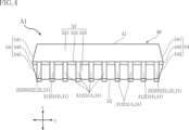
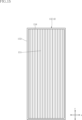
- FIG. 1 is a plan view of a semiconductor device according to a first embodiment of the present disclosure
- FIG. FIG. 2 is a plan view corresponding to FIG. 1, showing only the outer shape of the sealing resin.
- 3 is a front view of the semiconductor device shown in FIG. 1.
- FIG. 4 is a left side view of the semiconductor device shown in FIG. 1.
- FIG. 5 is a right side view of the semiconductor device shown in FIG. 1.
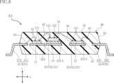
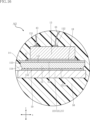
- FIG. 6 is a cross-sectional view taken along line VI-VI of FIG.
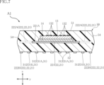
- FIG. 7 is a cross-sectional view along line VII-VII of FIG. 8 is a partially enlarged view of FIG. 2.
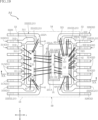
- FIG. 9 is a cross-sectional view along line IX-IX in FIG. 8.
- FIG. 10 is a schematic diagram of the insulating elements and dummy elements shown in FIG. 11 is a partially enlarged cross-sectional view of a semiconductor device according to a first modification of the first embodiment of the present disclosure
- FIG. FIG. 12 is a partially enlarged cross-sectional view of a semiconductor device according to a second modification of the first embodiment of the present disclosure
- 13 is a partially enlarged cross-sectional view of a semiconductor device according to a third modification of the first embodiment of the present disclosure
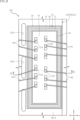
- FIG. FIG. 14 is a partially enlarged plan view of the semiconductor device according to the second embodiment of the present disclosure, omitting illustration of the sealing resin.
- 15 is a bottom view of the dummy element of the semiconductor device shown in FIG. 14.
- FIG. 16 is a cross-sectional view taken along line XVI--XVI of FIG. 14.
- FIG. 17 is a partially enlarged plan view of the semiconductor device according to the third embodiment of the present disclosure, omitting illustration of the sealing resin.
- 18 is a cross-sectional view taken along line XVIII-XVIII in FIG. 17.
- FIG. 19 is a plan view of the semiconductor device according to the fourth embodiment of the present disclosure, showing only the outer shape of the sealing resin.
- 20 is a cross-sectional view taken along line XX-XX in FIG. 19.
- FIG. FIG. 21 is a plan view of the semiconductor device according to the fifth embodiment of the present disclosure, showing only the outer shape of the sealing resin.
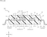
- FIG. 22 is a cross-sectional view taken along line XXII-XXII of FIG. 21.
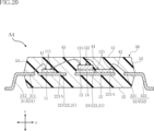
- FIG. 23 is a partially enlarged view of FIG. 21.
- FIG. 24 is a cross-sectional view along line XXIV-XXIV of FIG. 23.
- FIG. 25 is a schematic diagram of the insulating element and the dummy element shown in FIG. 24.
- FIG. FIG. 26 is a plan view of the semiconductor device according to the sixth embodiment of the present disclosure, showing only the outer shape of the sealing resin.
- 27 is a cross-sectional view taken along line XXVII-XXVII of FIG. 26.
- FIG. 28 is a partially enlarged view of FIG. 27.
- FIG. 1 A semiconductor device A1 according to the first embodiment of the present disclosure will be described based on FIGS. 1 to 10.
- FIG. The semiconductor device A1 includes a first semiconductor element 11, a second semiconductor element 12, an insulating element 13, a die pad 21, a plurality of first terminals 31, a plurality of second terminals 32, a dummy element 14, a first bonding layer 18, a second A bonding layer 19 and a sealing resin 50 are provided.
- the semiconductor device A1 further includes a plurality of first wires 41, a plurality of second wires 42, a plurality of third wires 43, and a plurality of fourth wires 44. As shown in FIG.
- the semiconductor device A1 is surface-mounted, for example, on a wiring board of an inverter device such as an electric vehicle or a hybrid vehicle.
- the package format of the semiconductor device A1 is SOP (Small Outline Package).
- SOP Small Outline Package
- the package format of the semiconductor device A1 is not limited to SOP.
- FIG. 2 shows only the outer shape of the sealing resin 50 for convenience of understanding. In FIG. 2, the outer shape of the sealing resin 50 is indicated by an imaginary line (chain double-dashed line).
- the thickness direction of the first semiconductor element 11 is called "thickness direction z".
- the thickness direction z corresponds to the normal direction of a first mounting surface 221A of a first pad portion 221 (first die pad 22), which will be described later.
- a direction perpendicular to the thickness direction z is called a “first direction x”.
- a direction orthogonal to both the thickness direction z and the first direction x is called a “second direction y”.
- the first semiconductor element 11, the second semiconductor element 12, and the insulating element 13 are elements that serve as functional centers of the semiconductor device A1.
- the first semiconductor element 11, the second semiconductor element 12 and the insulating element 13 are composed of individual elements.
- the second semiconductor element 12 is located on the opposite side of the insulating element 13 from the first semiconductor element 11 .
- the first semiconductor element 11, the second semiconductor element 12, and the insulating element 13 have a relatively elongated rectangular shape along the second direction y.
- the first semiconductor element 11 is a controller (control element) that controls a gate driver, which will be described later.
- the first semiconductor element 11 includes a circuit for converting an electrical signal input from another semiconductor device into a PWM control signal, a transmission circuit for transmitting the PWM control signal to the second semiconductor element 12, and a second semiconductor element. a receiving circuit for receiving electrical signals from 12;
- the second semiconductor element 12 is a gate driver (driving element) for driving the switching element.
- the switching element is, for example, an IGBT (Insulated Gate Bipolar Transistor) or a MOSFET (Metal-Oxide-Semiconductor Field-Effect Transistor).
- the second semiconductor element 12 includes a receiving circuit for receiving a PWM control signal, a circuit for driving the switching element based on the PWM control signal, and a transmitting circuit for transmitting an electrical signal to the first semiconductor element 11. equip.
- the electric signal is, for example, an output signal from a temperature sensor arranged near the motor.
- the isolation element 13 is an element for transmitting the PWM control signal and other electrical signals in an isolated state.
- the insulating element 13 is of the inductive type.
- An example of the inductive insulating element 13 is an insulating transformer.
- An isolation transformer performs electrical signal transmission in an insulated state by inductively coupling two inductors (coils).
- the insulating element 13 has a substrate made of silicon.
- An inductor made of copper (Cu) is formed on the substrate.
- the inductor includes a transmitting inductor and a receiving inductor, which are stacked in the thickness direction z.
- a dielectric layer made of silicon dioxide (SiO 2 ) or the like is interposed between the transmitting side inductor and the receiving side inductor. The dielectric layer electrically insulates the transmitting inductor from the receiving inductor.
- the insulating element 13 may be of the capacitive type.
- a capacitor is an example of the capacitive insulating element 13 .
- the voltage applied to the first semiconductor element 11 and the voltage applied to the second semiconductor element 12 are relatively different. Therefore, a potential difference is generated between the first semiconductor element 11 and the second semiconductor element 12 .
- the voltage applied to second semiconductor element 12 is higher than the voltage applied to first semiconductor element 11 .
- the power supply voltage supplied to the second semiconductor element 12 is higher than the power supply voltage supplied to the first semiconductor element 11.
- the first circuit including the first semiconductor element 11 as a component and the second circuit including the second semiconductor element 12 as a component are insulated from each other by the insulating element 13.
- the isolation element 13 is electrically connected to the first circuit and the second circuit.
- Components of the first circuit include, in addition to the first semiconductor element 11, a first die pad 22, a plurality of first terminals 31, a plurality of first wires 41, and a plurality of third wires 43, which will be described later.
- Components of the second circuit include, in addition to the second semiconductor element 12, a second die pad 23, a plurality of second terminals 32, a plurality of second wires 42, and a plurality of fourth wires 44, which will be described later.
- the potentials of the first circuit and the second circuit are relatively different.
- the potential of the second circuit is higher than the potential of the first circuit.
- the isolation element 13 then relays mutual signals in the first and second circuits.
- the voltage applied to the ground of the first semiconductor element 11 is approximately 0 V
- the voltage applied to the ground of the second semiconductor element 12 is transiently 600 V. It may be more than that.
- the first semiconductor element 11 has a plurality of first electrodes 111.
- the plurality of first electrodes 111 are provided on the upper surface of the first semiconductor element 11 (the surface facing the same direction as the first mounting surface 221A of the first pad portion 221 of the first die pad 22 described below).
- a composition of the plurality of first electrodes 111 includes, for example, aluminum (Al). That is, each first electrode 111 contains aluminum.
- the multiple first electrodes 111 are electrically connected to the circuit configured in the first semiconductor element 11 .
- the insulating element 13 is positioned between the first semiconductor element 11 and the second semiconductor element 12 in the first direction x.
- the insulating element 13 has multiple first relay electrodes 131 and multiple second relay electrodes 132 .
- the plurality of first relay electrodes 131 and the plurality of second relay electrodes 132 are provided on the upper surface of the insulating element 13 (the surface facing the same direction as the above-described first mounting surface 221A).
- the plurality of first relay electrodes 131 are arranged along the second direction y and positioned closer to the first semiconductor element 11 than the second semiconductor element 12 in the first direction x.
- the plurality of second relay electrodes 132 are arranged along the second direction y and positioned closer to the second semiconductor element 12 than to the first semiconductor element 11 in the first direction x.
- the insulating element 13 further has a first transmitter/receiver 133, a second transmitter/receiver 134, and a relay 135.
- the first transmitting/receiving section 133, the second transmitting/receiving section 134, and the relay section 135 are inductors.
- the first transceiver 133 and the second transceiver 134 are positioned apart from each other in the first direction x.
- the first transmitting/receiving section 133 is electrically connected to the plurality of first relay electrodes 131 .
- the first transmission/reception section 133 is electrically connected to the first semiconductor element 11 via the plurality of third wires 43 .
- the second transmitting/receiving section 134 is electrically connected to the plurality of second relay electrodes 132 .
- the second transmitter/receiver 134 is electrically connected to the second semiconductor element 12 via a plurality of fourth wires 44 .
- the relay section 135 is located apart from the first transmission/reception section 133 and the second transmission/reception section 134 in the thickness direction z.
- a dielectric layer (not shown) made of silicon dioxide or the like is interposed between the relay section 135 and the first transmitting/receiving section 133 and the second transmitting/receiving section 134 .
- the relay unit 135 transmits and receives signals between the first transmission/reception unit 133 and the second transmission/reception unit 134 .
- the relay portion 135 is positioned closer to the dummy element 14 than the first transceiver portion 133 and the second transceiver portion 134 in the thickness direction z.
- the potential of the relay section 135 takes a value between the potential of the first transmission/reception section 133 and the potential of the second transmission/reception section 134 .
- the second semiconductor element 12 has multiple second electrodes 121 .
- the plurality of second electrodes 121 are provided on the upper surface of the second semiconductor element 12 (the surface facing the same direction as the second mounting surface 231A of the second pad portion 231 of the second die pad 23 described below).
- the composition of the plurality of second electrodes 121 includes, for example, aluminum.
- the multiple second electrodes 121 are electrically connected to the circuit configured in the second semiconductor element 12 .
- the die pad 21, the plurality of first terminals 31, and the plurality of second terminals 32 form conduction paths between the first semiconductor element 11, the insulating element 13, the second semiconductor element 12, and the wiring substrate on which the semiconductor device A1 is mounted. Configure.
- the die pad 21, the plurality of first terminals 31, and the plurality of second terminals 32 are obtained from the same lead frame.
- the leadframe includes copper in its composition.
- die pad 21 includes first die pad 22 and second die pad 23 .
- the first die pad 22 and the second die pad 23 are positioned apart from each other in the first direction x, as shown in FIGS.
- the first semiconductor element 11 is mounted on the first die pad 22
- the second semiconductor element 12 is mounted on the second die pad .
- the voltage applied to the second die pad 23 is relatively different from the voltage applied to the first die pad 22 .
- the voltage applied to the second die pad 23 is higher than the voltage applied to the first die pad 22 .
- the first die pad 22 has a first pad portion 221 and two first suspension lead portions 222 .
- the first semiconductor element 11 is mounted on the first pad section 221 .
- the first pad portion 221 has a first mounting surface 221A facing the thickness direction z.
- the first semiconductor element 11 is bonded to the first mounting surface 221A via a conductive bonding material (solder, metal paste, etc.) not shown.
- the first pad portion 221 is covered with the sealing resin 50 .
- the thickness of first pad portion 221 is, for example, 150 ⁇ m or more and 200 ⁇ m or less.
- the first pad portion 221 has a plurality of through holes 223 formed therein.
- Each of the plurality of through holes 223 penetrates the first pad portion 221 in the thickness direction z and extends in the second direction y.
- At least one of the plurality of through holes 223 is positioned between the first semiconductor element 11 and the dummy element 14 when viewed in the thickness direction z.
- the plurality of through holes 223 are arranged along the second direction y.
- the two first suspension lead portions 222 are connected to both sides of the first pad portion 221 in the second direction y.
- the two first suspension lead portions 222 have covered portions 222A and exposed portions 222B.
- the covering portion 222A is connected to the first pad portion 221 and covered with the sealing resin 50 .
- the covering portion 222A includes a section extending in the first direction x.
- the exposed portion 222B is connected to the covered portion 222A and is exposed from the sealing resin 50 .
- the exposed portion 222B extends in the first direction x when viewed in the thickness direction z.
- the exposed portion 222B is bent in a gull-wing shape when viewed in the second direction y.
- the surface of exposed portion 222B may be plated with tin (Sn), for example.
- the second die pad 23 has a second pad portion 231 and two second suspension lead portions 232 .
- the second semiconductor element 12 is mounted on the second pad portion 231 .
- the second pad portion 231 has a second mounting surface 231A facing the thickness direction z.
- the second semiconductor element 12 is bonded to the second mounting surface 231A via a conductive bonding material (solder, metal paste, etc.) not shown.
- the second pad portion 231 is covered with the sealing resin 50 .
- the thickness of second pad portion 231 is, for example, 150 ⁇ m or more and 200 ⁇ m or less.
- the area of the second pad portion 231 is smaller than the area of the first pad portion 221 of the first die pad 22 .
- the second pad portion 231 overlaps the first pad portion 221 when viewed in the first direction x.
- the two second suspension lead portions 232 extend from both sides of the second pad portion 231 in the second direction y.
- the two second suspension lead portions 232 have covered portions 232A and exposed portions 232B.
- the covering portion 232A is connected to the second pad portion 231 and covered with the sealing resin 50 .
- the covering portion 232A includes a section extending in the first direction x.
- the exposed portion 232B is connected to the covered portion 232A and exposed from the sealing resin 50 .
- the exposed portion 232B extends in the first direction x when viewed in the thickness direction z.
- the exposed portion 232B is bent in a gull-wing shape when viewed in the second direction y.
- the surface of the exposed portion 232B may be plated with tin, for example.
- the dummy element 14 is bonded to the die pad 21 as shown in FIGS. As viewed in the thickness direction z, the dummy element 14 is located inside the peripheral edge of the die pad 21 . In the semiconductor device A1, the dummy element 14 is bonded to the first mounting surface 221A of the first pad portion 221 of the first die pad 22. As shown in FIG. The insulating element 13 is bonded to the dummy element 14 .
- the first bonding layer 18 bonds the dummy element 14 and the insulating element 13, as shown in FIG.
- the first bonding layer 18 is a conductor.
- the first bonding layer 18 is made of, for example, a die attach material. Alternatively, the first bonding layer 18 may be an insulator.
- the second bonding layer 19 bonds the die pad 21 and the dummy element 14, as shown in FIG.
- the second bonding layer 19 is a conductor.
- the second bonding layer 19 is made of the same material as the first bonding layer 18 .
- dummy element 14 includes semiconductor substrate 15 and insulating layer 16 .
- the insulating layer 16 is laminated on the semiconductor substrate 15 .
- Semiconductor substrate 15 is, for example, a silicon wafer containing a p-type dopant.
- Insulating layer 16 is made of an insulating material selected from silicon dioxide, silicon nitride (Si 3 N 4 ), polyimide, and the like. The insulating layer 16 is positioned between the die pad 21 and the first bonding layer 18 in the thickness direction z.
- the semiconductor substrate 15 has a first surface 151, a second surface 152 and a third surface 153.
- the first surface 151 faces the thickness direction z and faces the first bonding layer 18 .
- the second surface 152 faces the side opposite to the first surface 151 in the thickness direction z and faces the second bonding layer 19 .
- the third surface 153 faces a direction perpendicular to the thickness direction z.
- the insulating layer 16 is stacked on the first surface 151 in the semiconductor device A1. Therefore, the insulating layer 16 is located between the semiconductor substrate 15 and the first bonding layer 18 .
- the insulating layer 16 is in contact with the first bonding layer 18 .
- the dummy element 14 is formed with a protrusion 17 protruding from the insulating layer 16 in the thickness direction z.
- the convex portion 17 is located outside the first bonding layer 18 when viewed in the thickness direction z.
- the convex portion 17 surrounds the first bonding layer 18 .
- the protrusion 17 is an insulator like the insulating layer 16 .
- the protrusions 17 are made of an insulating material selected from silicon dioxide, silicon nitride, polyimide, and the like. Therefore, the convex portion 17 may be configured integrally with the insulating layer 16 .
- the dimension of the convex portion 17 in the thickness direction z is smaller than the dimension of the first bonding layer 18 in the thickness direction z.
- the plurality of first terminals 31 are located on the opposite side of the second semiconductor element 12 with respect to the insulating element 13 in the first direction x.
- the multiple first terminals 31 are arranged along the second direction y. At least one of the plurality of first terminals 31 is electrically connected to the first semiconductor element 11 via the third wire 43 .
- the plurality of first terminals 31 are positioned between the two first hanging lead portions 222 of the first die pad 22 in the second direction y.
- the multiple first terminals 31 include multiple first intermediate terminals 31A and two first side terminals 31B.
- the two first side terminals 31B are located on both sides of the plurality of first intermediate terminals 31A in the second direction y.
- the plurality of first terminals 31 have covered portions 311 and exposed portions 312 .
- the covering portion 311 is covered with the sealing resin 50 .
- the dimension of the covering portion 311 of each of the two first side terminals 31B in the first direction x is larger than the dimension of the covering portion 311 of each of the plurality of first intermediate terminals 31A in the first direction x.
- the exposed portion 312 is connected to the covering portion 311 and exposed from the sealing resin 50 .
- the exposed portion 312 extends in the first direction x when viewed in the thickness direction z.
- the exposed portion 312 is bent in a gull-wing shape when viewed in the second direction y.
- the shape of the exposed portion 312 is the same as the shape of the exposed portion 222B of each of the two first hanging lead portions 222 of the first die pad 22 .
- the surface of the exposed portion 312 may be plated with tin, for example.
- the plurality of second terminals 32 are located on the opposite side of the first semiconductor element 11 with respect to the insulating element 13 in the first direction x.
- the multiple second terminals 32 are arranged along the second direction y. At least one of the plurality of second terminals 32 is electrically connected to the second semiconductor element 12 via the fourth wire 44 .
- the multiple second terminals 32 include multiple second intermediate terminals 32A and two second side terminals 32B. Two second hanging lead portions 232 of the second die pad 23 are positioned on both sides of the plurality of second intermediate terminals 32A in the second direction y.
- the two second side terminals 32B are positioned so as to sandwich the plurality of second intermediate terminals 32A and the two second suspension lead portions 232 in the second direction y.
- the plurality of second terminals 32 have covered portions 321 and exposed portions 322 .
- the covering portion 321 is covered with the sealing resin 50 .
- the dimension of the covering portion 321 of each of the two second side terminals 32B in the first direction x is larger than the dimension of the covering portion 321 of each of the plurality of second intermediate terminals 32A in the first direction x.
- the exposed portion 322 is connected to the covering portion 321 and exposed from the sealing resin 50 .
- the exposed portion 322 extends in the first direction x when viewed in the thickness direction z.
- the exposed portion 322 is bent in a gull-wing shape when viewed in the second direction y.
- the shape of the exposed portion 322 is equal to the shape of the exposed portion 232B of each of the two second suspension lead portions 232 of the second die pad 23 .
- the surface of the exposed portion 322 may be plated with tin, for example.
- the plurality of first wires 41 , the plurality of second wires 42 , the plurality of third wires 43 , and the plurality of fourth wires 44 are connected together with the die pad 21 , the plurality of first terminals 31 , and the plurality of second terminals 32 .
- the first semiconductor element 11, the second semiconductor element 12 and the insulating element 13 form a conducting path for performing a predetermined function.
- the plurality of first wires 41 are joined to the plurality of first electrodes 111 of the first semiconductor element 11 and the covering portions 311 of the plurality of first terminals 31, as shown in FIGS. Accordingly, at least one of the plurality of first terminals 31 is electrically connected to the first semiconductor element 11 . Furthermore, at least one of the plurality of first wires 41 is joined to one of the plurality of first electrodes 111 and one of the covering portions 222A of the two first hanging lead portions 222 of the first die pad 22 . As a result, at least one of the two first hanging lead portions 222 is electrically connected to the first semiconductor element 11 . As a result, at least one of the two first suspension lead portions 222 serves as a ground terminal of the first semiconductor element 11 .
- the composition of the plurality of first wires 41 includes gold (Au). Alternatively, the composition of the plurality of first wires 41 may contain copper.
- the plurality of second wires 42 are joined to the plurality of second electrodes 121 of the second semiconductor element 12 and the covering portions 321 of the plurality of second terminals 32, as shown in FIGS. As a result, at least one of the plurality of second terminals 32 is electrically connected to the second semiconductor element 12 . Furthermore, at least one of the plurality of second wires 42 is joined to one of the plurality of second electrodes 121 and one of the covering portions 232A of the two second suspension lead portions 232 of the second die pad 23 . As a result, at least one of the two second suspension lead portions 232 is electrically connected to the second semiconductor element 12 . As a result, at least one of the two second hanging lead portions 232 serves as a ground terminal of the second semiconductor element 12 .
- the composition of the plurality of second wires 42 includes gold. Alternatively, the composition of the plurality of second wires 42 may contain copper.
- the plurality of third wires 43 are joined to the plurality of first relay electrodes 131 of the insulating element 13 and the plurality of first electrodes 111 of the first semiconductor element 11, as shown in FIGS. Thereby, the first semiconductor element 11 and the insulating element 13 are electrically connected to each other.
- the multiple third wires 43 are arranged along the second direction y.
- the composition of the plurality of third wires 43 contains gold.
- the plurality of fourth wires 44 are joined to the plurality of second relay electrodes 132 of the insulating element 13 and the plurality of second electrodes 121 of the second semiconductor element 12, as shown in FIGS. Thereby, the second semiconductor element 12 and the insulating element 13 are electrically connected to each other.
- the multiple fourth wires 44 are arranged along the second direction y. In the semiconductor device A ⁇ b>1 , the plurality of fourth wires 44 straddle between the first pad portion 221 of the first die pad 22 and the second pad portion 231 of the second die pad 23 .
- the composition of the plurality of fourth wires 44 includes gold.
- the sealing resin 50 is applied to the first semiconductor element 11, the second semiconductor element 12, the insulating element 13, the die pad 21, the plurality of first terminals 31, and the plurality of second terminals 32, respectively. cover at least part of each. Furthermore, the sealing resin 50 covers the plurality of first wires 41 , the plurality of second wires 42 , the plurality of third wires 43 , and the plurality of fourth wires 44 .
- the sealing resin 50 has electrical insulation. Sealing resin 50 is made of a material containing epoxy resin, for example.
- the sealing resin 50 has a rectangular shape when viewed in the thickness direction z.
- the sealing resin 50 has a top surface 51, a bottom surface 52, a pair of first side surfaces 53, and a pair of second side surfaces .
- top surface 51 and the bottom surface 52 are positioned apart from each other in the thickness direction z.
- the top surface 51 and the bottom surface 52 face opposite sides in the thickness direction z.
- Each of top surface 51 and bottom surface 52 is flat (or substantially flat).
- the pair of first side surfaces 53 are connected to the top surface 51 and the bottom surface 52 and are separated from each other in the first direction x.
- the exposed portions 222B of the two first suspension lead portions 222 of the first die pad 22 and the plurality of first terminals 31 and the exposed portion 312 of are exposed.
- the exposed portions 222B of the two second suspension lead portions 232 of the second die pad 23, the plurality of second terminals 32 and the exposed portion 322 of are exposed.
- Each of the pair of first side surfaces 53 includes a first upper portion 531, a first lower portion 532 and a first intermediate portion 533, as shown in FIGS.
- One side of the first upper portion 531 in the thickness direction z is connected to the top surface 51 , and the other side in the thickness direction z is connected to the first intermediate portion 533 .
- the first upper portion 531 is inclined with respect to the top surface 51 .
- One side of the first lower portion 532 in the thickness direction z is connected to the bottom surface 52 , and the other side in the thickness direction z is connected to the first intermediate portion 533 .
- the first lower portion 532 is inclined with respect to the bottom surface 52 .
- first intermediate portion 533 in the thickness direction z is connected to the first upper portion 531 , and the other side in the thickness direction z is connected to the first lower portion 532 .
- the in-plane directions of the first intermediate portion 533 are the thickness direction z and the second direction y.
- the first intermediate portion 533 is located outside the top surface 51 and the bottom surface 52 when viewed in the thickness direction z. From the first intermediate portions 533 of the pair of first side surfaces 53, the exposed portions 222B of the two first suspension lead portions 222 of the first die pad 22 and the exposed portions 222B of the two second suspension lead portions 232 of the second die pad 23 are exposed. , the exposed portions 312 of the plurality of first terminals 31 and the exposed portions 322 of the plurality of second terminals 32 are exposed.
- the pair of second side surfaces 54 are connected to the top surface 51 and the bottom surface 52 and are separated from each other in the second direction y. As shown in FIG. 1 , the first die pad 22 , the second die pad 23 , the plurality of first terminals 31 , and the plurality of second terminals 32 are positioned away from the pair of second side surfaces 54 .
- each of the pair of second side surfaces 54 includes a second upper portion 541, a second lower portion 542 and a second intermediate portion 543.
- One side of the second upper portion 541 in the thickness direction z is connected to the top surface 51 , and the other side in the thickness direction z is connected to the second intermediate portion 543 .
- the second upper portion 541 is inclined with respect to the top surface 51 .
- One side of the second lower portion 542 in the thickness direction z is connected to the bottom surface 52 , and the other side in the thickness direction z is connected to the second intermediate portion 543 .
- the second lower portion 542 is inclined with respect to the bottom surface 52 .
- the second intermediate portion 543 has one side in the thickness direction z connected to the second upper portion 541 and the other side in the thickness direction z connected to the second lower portion 542 .
- the in-plane directions of the second intermediate portion 543 are the thickness direction z and the second direction y.
- the second intermediate portion 543 is located outside the top surface 51 and the bottom surface 52 when viewed in the thickness direction z.
- a half-bridge circuit including a low-side (low-potential side) switching element and a high-side (high-potential side) switching element.
- these switching elements are MOSFETs.
- the low-side switching element both the source of the switching element and the reference potential of the gate driver that drives the switching element are grounded.
- both the reference potential of the source of the switching element and the reference potential of the gate driver that drives the switching element correspond to the potential at the output node of the half bridge circuit.
- the reference potential of the gate driver that drives the high-side switching element changes.
- the reference potential is equivalent to the voltage applied to the drain of the high-side switching element (for example, 600V or higher).
- the semiconductor device A1 the ground of the first semiconductor element 11 and the ground of the second semiconductor element 12 are separated. Therefore, when the semiconductor device A1 is used as a gate driver for driving the high-side switching element, a transient voltage equivalent to the voltage applied to the drain of the high-side switching element is applied to the ground of the second semiconductor element 12. applied
- a semiconductor device A11 which is a first modification of the semiconductor device A1
- the semiconductor device A11 differs from the semiconductor device A1 in the configuration of the dummy element 14 .
- the cross-sectional position of FIG. 11 corresponds to the cross-sectional position of FIG.
- the insulating layer 16 is laminated on the second surface 152 of the semiconductor substrate 15, as shown in FIG. Therefore, the insulating layer 16 is positioned between the second bonding layer 19 and the semiconductor substrate 15 in the thickness direction z. The insulating layer 16 is in contact with the second bonding layer 19 . The convex portion 17 is formed in contact with the first surface 151 of the semiconductor substrate 15 .
- a semiconductor device A12 which is a second modification of the semiconductor device A1
- the semiconductor device A12 differs from the semiconductor device A1 in the configuration of the dummy element 14 .
- the cross-sectional position of FIG. 12 corresponds to the cross-sectional position of FIG.
- the insulating layer 16 includes a first layer 16A and a second layer 16B.
- the second layer 16B is located away from the first layer 16A in the thickness direction z.
- the first layer 16A is laminated on the first surface 151 of the semiconductor substrate 15 . Therefore, the first layer 16A is positioned between the semiconductor substrate 15 and the first bonding layer 18 in the thickness direction z.
- the first layer 16A is in contact with the first bonding layer 18 .
- the second layer 16B is laminated on the second surface 152 of the semiconductor substrate 15 . Therefore, the second layer 16B is positioned between the second bonding layer 19 and the semiconductor substrate 15 in the thickness direction z.
- the second layer 16B is in contact with the second bonding layer 19 .
- a semiconductor device A13 which is a third modification of the semiconductor device A1
- the semiconductor device A13 differs from the semiconductor device A1 in the configuration of the dummy element 14 .
- the cross-sectional position of FIG. 13 corresponds to the cross-sectional position of FIG.
- the semiconductor substrate 15 includes a first substrate 15A and a second substrate 15B.
- the second substrate 15B is positioned apart from the first substrate 15A in the thickness direction z.
- the first substrate 15A is in contact with the first bonding layer 18 .
- the second substrate 15B is positioned between the second bonding layer 19 and the first substrate 15A in the thickness direction z and is in contact with the second bonding layer 19 .
- the insulating layer 16 is positioned between the second substrate 15B and the first substrate 15A in the thickness direction z.
- the insulating layer 16 includes a first layer 16A laminated on the first substrate 15A and a second layer 16B laminated on the second substrate 15B.
- the second layer 16B faces the first layer 16A.
- insulating layer 16 may be of a single construction that does not include first layer 16A and second layer 16B.
- the semiconductor device A1 includes a die pad 21, a first semiconductor element 11 and a second semiconductor element 12 mounted on the die pad 21, and an insulating element 13 for insulating the first semiconductor element 11 and the second semiconductor element 12 from each other. and
- the semiconductor device A1 further includes a dummy element 14 bonded to the die pad 21 and a first bonding layer 18 bonding the dummy element 14 and the insulating element 13 together.
- the dummy element 14 includes an insulating layer 16 located between the die pad 21 and the first bonding layer 18 in the thickness direction z.
- dielectric breakdown of the insulating element 13 occurs when charged carriers move from the die pad 21 to the insulating element 13 .
- the movement of the carrier from the upper surface of the die pad 21 (the first mounting surface 221A of the first pad portion 221 of the first die pad 22) to the lower surface of the insulating element 13 facing the upper surface is insulated. blocked by layer 16; This makes it difficult for the insulating element 13 to break down. Therefore, according to the semiconductor device A1, it is possible to improve the withstand voltage between the die pad 21 on which a plurality of semiconductor elements (the first semiconductor element 11 and the second semiconductor element 12) are mounted and the insulating element 13. becomes.
- the dummy element 14 includes the semiconductor substrate 15 in addition to the insulating layer 16 .
- the insulating layer 16 is laminated on the semiconductor substrate 15 .
- the insulating layer 16 includes a first layer 16A and a second layer 16B located apart from the first layer 16A.
- the first layer 16A is located between the semiconductor substrate 15 and the first bonding layer 18 .
- the second layer 16B is positioned between the second bonding layer 19 and the semiconductor substrate 15 .
- the dummy element 14 is formed with a protrusion 17 protruding from the insulating layer 16 in the thickness direction z.
- the convex portion 17 is located outside the first bonding layer 18 when viewed in the thickness direction z.
- the insulating element 13 has a first transmission/reception section 133 , a second transmission/reception section 134 and a relay section 135 .
- the relay portion 135 is positioned closer to the dummy element 14 than the first transceiver portion 133 and the second transceiver portion 134 in the thickness direction z.
- the dummy element 14 is located inside the peripheral edge of the die pad 21 when viewed in the thickness direction z. As a result, it is possible to prevent the semiconductor device A1 from increasing in size.
- the semiconductor device A ⁇ b>1 part of each of the die pad 21 , the plurality of first terminals 31 , and the plurality of second terminals 32 are exposed from either one of the pair of first side surfaces 53 of the sealing resin 50 .
- the two first suspension lead portions 222 of the first die pad 22 are exposed from one side of the sealing resin 50 in the first direction x, and the two second suspension lead portions 232 of the second die pad 23 are sealed. It is obtained by exposing the stopper resin 50 from the other side in the first direction x.
- the die pad 21 , the plurality of first terminals 31 , and the plurality of second terminals 32 are positioned apart from the pair of second side surfaces 54 of the sealing resin 50 . Thereby, all of the die pad 21 , the plurality of first terminals 31 , and the plurality of second terminals 32 are not exposed from the pair of second side surfaces 54 .
- This configuration contributes to the improvement of the withstand voltage of the semiconductor device A1.
- a plurality of through holes 223 are formed in the first pad portion 221 of the first die pad 22 having a larger area than the second pad portion 231 of the second die pad 23.
- the fluidized sealing resin 50 passes through the plurality of through-holes 223 in the manufacture of the semiconductor device A1, so that filling defects of the sealing resin 50 can be prevented. Therefore, it is possible to effectively suppress the formation of voids in the sealing resin 50 . This contributes to suppressing a decrease in the breakdown voltage of the semiconductor device A1.
- FIG. 14 omits illustration of the sealing resin 50 for convenience of understanding.
- the configuration of the dummy element 14 is different from that of the semiconductor device A1.
- the semiconductor substrate 15 has a first recess 154 formed therein.
- the first concave portion 154 is recessed from the second surface 152 and the third surface 153 of the semiconductor substrate 15 .
- the first recess 154 surrounds the second surface 152 .
- the first concave portion 154 can be formed by half-cut dicing the silicon wafer that is the base of the semiconductor substrate 15 .
- the surface roughness of the second surface 152 of the semiconductor substrate 15 is greater than the surface roughness of the third surface 153 of the semiconductor substrate 15 .
- the second surface 152 of this configuration is obtained by subjecting a silicon wafer, which is the base of the semiconductor substrate 15, to mechanical grinding.
- the second bonding layer 19 is surrounded by the periphery of the dummy element 14 when viewed in the thickness direction z.
- the semiconductor device A2 includes a die pad 21, a first semiconductor element 11 and a second semiconductor element 12 mounted on the die pad 21, and an insulating element 13 for insulating the first semiconductor element 11 and the second semiconductor element 12 from each other. and
- the semiconductor device A2 further includes a dummy element 14 bonded to the die pad 21 and a first bonding layer 18 bonding the dummy element 14 and the insulating element 13 together.
- the dummy element 14 includes an insulating layer 16 located between the die pad 21 and the first bonding layer 18 in the thickness direction z. Therefore, even with the semiconductor device A2, it is possible to improve the withstand voltage between the die pad 21 on which a plurality of semiconductor elements (the first semiconductor element 11 and the second semiconductor element 12) are mounted and the insulating element 13. Become. Furthermore, the semiconductor device A2 has the same effect as the semiconductor device A1 by adopting a configuration common to the semiconductor device A1.
- the semiconductor substrate 15 is formed with first recesses 154 that are recessed from the second surface 152 and the third surface 153 .
- the creeping distance of the dummy element 14 from the first bonding layer 18 to the second bonding layer 19 becomes longer.
- the moving distance of charged carriers from the upper surface of the die pad 21 to the lower surface of the insulating element 13 becomes longer, so that the breakdown voltage between the die pad 21 and the insulating element 13 increases compared to the configuration of the semiconductor device A1. improve more.
- the first concave portion 154 surrounds the second surface 152, this effect can be exhibited more effectively.
- the second bonding layer 19 is surrounded by the periphery of the dummy element 14 when viewed in the thickness direction z. This configuration is obtained by suppressing the second bonding layer 19 from crawling up the dummy element 14 by the first concave portion 154 when the dummy element 14 is bonded to the die pad 21 via the second bonding layer 19 . By suppressing the second bonding layer 19 from crawling up the dummy element 14 , shortening of the creepage distance of the dummy element 14 from the first bonding layer 18 to the second bonding layer 19 can be avoided. This configuration is particularly effective when the second bonding layer 19 is a conductor in contact with the semiconductor substrate 15 .
- the surface roughness of the second surface 152 of the semiconductor substrate 15 is greater than the surface roughness of the third surface 153 of the semiconductor substrate 15 .
- the second bonding layer 19 can exhibit an anchor effect with respect to the semiconductor substrate 15 . Therefore, the bonding strength of the dummy element 14 to the die pad 21 can be improved.
- FIG. 17 omits illustration of the sealing resin 50 for convenience of understanding.
- the configuration of the dummy element 14 is different from the above-described configuration of the semiconductor device A2.
- the semiconductor substrate 15 is formed with a second recess 155 in addition to the first recess 154 .
- the configuration of the first recess 154 is the same as that of the semiconductor device A2.
- the second recess 155 is recessed from the first surface 151 and the third surface 153 of the semiconductor substrate 15 .
- the second recess 155 overlaps the first recess 154 when viewed in the thickness direction z.
- the second recess 155 surrounds the first surface 151 .
- the semiconductor device A3 includes a die pad 21, a first semiconductor element 11 and a second semiconductor element 12 mounted on the die pad 21, and an insulating element 13 for insulating the first semiconductor element 11 and the second semiconductor element 12 from each other. and
- the semiconductor device A3 further includes a dummy element 14 bonded to the die pad 21 and a first bonding layer 18 bonding the dummy element 14 and the insulating element 13 together.
- the dummy element 14 includes an insulating layer 16 located between the die pad 21 and the first bonding layer 18 in the thickness direction z. Therefore, even with the semiconductor device A3, it is possible to improve the withstand voltage between the die pad 21 on which a plurality of semiconductor elements (the first semiconductor element 11 and the second semiconductor element 12) are mounted and the insulating element 13. Become. Furthermore, the semiconductor device A3 has the same effect as the semiconductor device A1 by adopting a structure common to the semiconductor device A1.
- the semiconductor substrate 15 is formed with a first recess 154 recessed from the second surface 152 and the third surface 153, and a second recess 155 recessed from the first surface 151 and the third surface 153. .
- the second recess 155 overlaps the first recess 154 when viewed in the thickness direction z.
- the moving distance of charged carriers from the upper surface of the die pad 21 to the lower surface of the insulating element 13 is further increased, so that the breakdown voltage between the die pad 21 and the insulating element 13 is increased as compared with the configuration of the semiconductor device A1. Further improve. Furthermore, when the first concave portion 154 surrounds the first surface 151, this effect can be exhibited more effectively.
- FIG. 19 shows only the outer shape of the sealing resin 50 for convenience of understanding.
- the outline of the sealing resin 50 is indicated by imaginary lines.
- the configurations of the insulating elements 13 and the dummy elements 14 are different from those of the semiconductor device A1.
- the dummy element 14 is bonded to the second mounting surface 231A of the second pad portion 231 of the second die pad 23.
- the insulating element 13 is positioned on the second pad portion 231 together with the second semiconductor element 12 .
- the dummy element 14 is bonded to the second mounting surface 231A via the second bonding layer 19 (see FIG. 9).
- the insulating element 13 is bonded to the dummy element 14 via the first bonding layer 18 . Therefore, in the semiconductor device A4, a plurality of third wires 43 straddle between the first pad portion 221 and the second pad portion 231 of the first die pad 22. As shown in FIG. Thus, even when the potential of the second pad section 231 is higher than the potential of the first pad section 221, the insulating element 13 can be mounted on the second pad section 231.
- the semiconductor device A4 includes a die pad 21, a first semiconductor element 11 and a second semiconductor element 12 mounted on the die pad 21, and an insulating element 13 for insulating the first semiconductor element 11 and the second semiconductor element 12 from each other. and
- the semiconductor device A4 further includes a dummy element 14 bonded to the die pad 21 and a first bonding layer 18 bonding the dummy element 14 and the insulating element 13 together.
- the dummy element 14 includes an insulating layer 16 located between the die pad 21 and the first bonding layer 18 in the thickness direction z. Therefore, even with the semiconductor device A4, it is possible to improve the withstand voltage between the die pad 21 on which a plurality of semiconductor elements (the first semiconductor element 11 and the second semiconductor element 12) are mounted and the insulating element 13. Become. Furthermore, the semiconductor device A4 has the same effect as the semiconductor device A1 by adopting a structure common to the semiconductor device A1.
- FIG. 21 shows only the outer shape of the sealing resin 50 for convenience of understanding.
- the outline of the sealing resin 50 is indicated by imaginary lines.
- semiconductor device A5 the configuration of the insulating element 13 is different from that of the semiconductor device A1.
- Semiconductor device A5 further includes a plurality of fifth wires 45 .
- the insulating element 13 includes a first insulating element 13A and a second insulating element 13B that are spaced apart from each other.
- first insulating element 13A and second insulating element 13B are separated from each other in first direction x so that first insulating element 13A is closer to first semiconductor element 11 than second insulating element 13B. located.
- the first insulating element 13A and the second insulating element 13B are bonded to the dummy element 14 via the first bonding layer 18 .
- the first bonding layer 18 is integrated.
- the first bonding layer 18 may be separated from each other like the first insulating element 13A and the second insulating element 13B.
- the dummy element 14 is bonded to the first mounting surface 221A of the first pad portion 221 of the first die pad 22 via the second bonding layer 19.
- the dummy element 14 may be bonded to the second mounting surface 231A of the second pad portion 231 of the second die pad 23, as in the semiconductor device A4 described above.
- the first insulating element 13A has multiple first relay electrodes 131 and multiple second relay electrodes 132 .
- the multiple third wires 43 are joined to the multiple first relay electrodes 131 and the multiple first electrodes 111 of the first semiconductor element 11 . Therefore, the plurality of first relay electrodes 131 are electrically connected to the first semiconductor element 11 .
- the first insulating element 13A has a first transmission/reception section 133 and a second transmission/reception section .
- the first transmitting/receiving section 133 and the second transmitting/receiving section 134 are inductors.
- the first transceiver 133 and the second transceiver 134 are positioned apart from each other in the thickness direction z.
- a dielectric layer (not shown) made of silicon dioxide or the like is interposed between the first transmitting/receiving section 133 and the second transmitting/receiving section 134 .
- the first transmitting/receiving section 133 is electrically connected to the plurality of first relay electrodes 131 .
- the first transmitting/receiving section 133 is electrically connected to the first semiconductor element 11 .
- the second transceiver 134 transmits and receives signals to and from the first transceiver 133 .
- the second transmitting/receiving section 134 is electrically connected to the plurality of second relay electrodes 132 .
- the second transceiver 134 is positioned closer to the dummy element 14 than the first transceiver 133 in the thickness direction z.
- the second insulating element 13B has multiple third relay electrodes 136 and multiple fourth relay electrodes 137 .
- the multiple fourth wires 44 are joined to the multiple fourth relay electrodes 137 and the multiple second electrodes 121 of the second semiconductor element 12 . Therefore, the plurality of fourth relay electrodes 137 are electrically connected to the second semiconductor element 12 .
- the second insulating element 13B has a third transceiver 138 and a fourth transceiver 139 .
- the third transmitting/receiving section 138 and the fourth transmitting/receiving section 139 are inductors.
- the third transceiver 138 and the fourth transceiver 139 are positioned apart from each other in the thickness direction z.
- a dielectric layer (not shown) made of silicon dioxide or the like is interposed between the third transmitting/receiving section 138 and the fourth transmitting/receiving section 139 in the second insulating element 13B.
- the fourth transmission/reception section 139 is electrically connected to the plurality of fourth relay electrodes 137 .
- the fourth transmitting/receiving section 139 is electrically connected to the second semiconductor element 12 .
- the third transceiver 138 transmits and receives signals to and from the fourth transceiver 139 .
- the third transmitting/receiving section 138 is electrically connected to the plurality of third relay electrodes 136 .
- the third transceiver section 138 is positioned closer to the dummy element 14 than the fourth transceiver section 139 in the thickness direction z.
- the plurality of fifth wires 45 are joined to the plurality of third relay electrodes 136 of the second insulation element 13B and the plurality of first relay electrodes 131 of the first insulation element 13A. ing.
- the composition of the plurality of fifth wires 45 includes gold.
- the plurality of second relay electrodes 132 and the plurality of third relay electrodes 136 are electrically connected to each other. Therefore, the third transmitting/receiving section 138 of the second insulating element 13B is electrically connected to the second transmitting/receiving section 134 of the first insulating element 13A. Therefore, the potential of the third transceiver 138 is equal to the potential of the second transceiver 134 .
- the potentials of the second transmitting/receiving section 134 and the third transmitting/receiving section 138 are between the potential of the first transmitting/receiving section 133 of the first insulating element 13A and the potential of the fourth transmitting/receiving section 139 of the second insulating element 13B. take a value.
- the semiconductor device A5 includes a die pad 21, a first semiconductor element 11 and a second semiconductor element 12 mounted on the die pad 21, and an insulating element 13 for insulating the first semiconductor element 11 and the second semiconductor element 12 from each other. and
- the semiconductor device A5 further includes a dummy element 14 bonded to the die pad 21 and a first bonding layer 18 bonding the dummy element 14 and the insulating element 13 together.
- the dummy element 14 includes an insulating layer 16 located between the die pad 21 and the first bonding layer 18 in the thickness direction z. Therefore, even with the semiconductor device A5, it is possible to improve the withstand voltage between the die pad 21 on which a plurality of semiconductor elements (the first semiconductor element 11 and the second semiconductor element 12) are mounted and the insulating element 13. Become. Further, the semiconductor device A5 has the same effect as the semiconductor device A1 by adopting a structure common to the semiconductor device A1.
- the insulating element 13 of the semiconductor device A5 includes a first insulating element 13A and a second insulating element 13B located apart from each other.
- the first insulating element 13A has a first transceiver section 133 and a second transceiver section 134 .
- the second isolation element 13B has a third transceiver 138 and a fourth transceiver 139 .
- the third transceiver 138 is electrically connected to the second transceiver 134 .
- the second transceiver 134 and the third transceiver 138 are located closer to the dummy element 14 than the first transceiver 133 and the fourth transceiver 139 .
- the potential difference between the first transmitting/receiving section 133 and the second transmitting/receiving section 134 can be set small.
- the potential difference between the third transmitting/receiving section 138 and the fourth transmitting/receiving section 139 can be set small. That is, the potential difference generated in each of the first insulating element 13A and the second insulating element 13B is reduced. Furthermore, the potential difference between the die pad 21 and the isolation element 13 is also reduced. Therefore, it becomes possible to more effectively improve the withstand voltage between the die pad 21 and the insulating element 13 .
- the semiconductor device A5 unlike the semiconductor device A1, it is not necessary to provide the relay portion 135 in the insulating element 13.
- FIG. 26 shows only the outer shape of the sealing resin 50 for convenience of understanding.
- the outline of the sealing resin 50 is indicated by imaginary lines.
- the configurations of the second semiconductor element 12 and the die pad 21 are different from those of the aforementioned semiconductor device A1.
- the die pad 21 is a single member that does not include the first die pad 22 and the second die pad 23.
- the die pad 21 has a pad portion 211 and two hanging lead portions 212 .
- the first semiconductor element 11 and the second semiconductor element 12 are located on the pad portion 211 .
- the pad portion 211 has a mounting surface 211A facing the thickness direction z.
- the first semiconductor element 11 is bonded to the mounting surface 211A via a conductive bonding material (solder, metal paste, etc.) not shown.
- the dummy element 14 is bonded to the mounting surface 211A via the second bonding layer 19.
- the pad portion 211 is covered with the sealing resin 50 .
- the thickness of pad portion 211 is, for example, 150 ⁇ m or more and 200 ⁇ m or less.
- the pad portion 211 has a plurality of through holes 213 formed therein.
- Each of the plurality of through holes 213 penetrates the pad portion 211 in the thickness direction z and extends in the second direction y.
- At least one of the plurality of through holes 213 is positioned between the first semiconductor element 11 and the dummy element 14 when viewed in the thickness direction z.
- the plurality of through holes 213 are arranged along the second direction y.
- the two hanging lead portions 212 are connected to both sides of the pad portion 211 in the second direction y.
- the two suspension lead portions 212 have covered portions 212A and exposed portions 212B.
- the covering portion 212A is connected to the pad portion 211 and covered with the sealing resin 50 .
- the covering portion 212A includes a section extending in the first direction x.
- the exposed portion 212B is connected to the covering portion 222A and is exposed from the first side surface 53 of the pair of first side surfaces 53 of the sealing resin 50 where the exposed portions 312 of the plurality of first terminals 31 are exposed.
- the exposed portion 222B extends in the first direction x when viewed in the thickness direction z. When viewed in the second direction y, the exposed portion 222B is bent in a gull-wing shape.
- the surface of the exposed portion 222B may be plated with tin, for example.
- At least one of the plurality of first wires 41 is bonded to one of the plurality of first electrodes 111 of the first semiconductor element 11 and one of the covering portions 212A of the two hanging lead portions 212. It is As a result, at least one of the two hanging lead portions 212 forms a ground terminal electrically connected to the first semiconductor element 11 .
- the second semiconductor element 12 is bonded to the dummy element 14 with the first bonding layer 18 interposed therebetween.
- the dummy element 14 is interposed between the die pad 21 and the second semiconductor element 12 and the insulating element 13, and the second semiconductor element 12 and the insulating element 13 are joined to the dummy element 14. configuration.
- the area of the dummy element 14 is larger than the area of the dummy element 14 of the semiconductor device A1.
- the plurality of fourth wires 44 are positioned inside the peripheral edge 241 of the dummy element 14 .
- At least one of the plurality of second wires 42 is connected to one of the plurality of second electrodes 121 of the second semiconductor element 12 and two second side terminals 32B (the plurality of second terminals 32). is joined to any one of the covering portions 321 of .
- at least one of the two second side terminals 32 ⁇ /b>B serves as a ground terminal electrically connected to the second semiconductor element 12 .
- the semiconductor device A6 includes a die pad 21, a first semiconductor element 11 and a second semiconductor element 12 mounted on the die pad 21, and an insulating element 13 for insulating the first semiconductor element 11 and the second semiconductor element 12 from each other. and The semiconductor device A6 further includes a dummy element 14 bonded to the die pad 21 and a first bonding layer 18 bonding the dummy element 14 and the insulating element 13 together.
- the dummy element 14 includes an insulating layer 16 located between the die pad 21 and the first bonding layer 18 in the thickness direction z. Therefore, even with the semiconductor device A6, it is possible to improve the withstand voltage between the die pad 21 on which a plurality of semiconductor elements (the first semiconductor element 11 and the second semiconductor element 12) are mounted and the insulating element 13. Become. Furthermore, the semiconductor device A6 has the same effect as the semiconductor device A1 by adopting a structure common to the semiconductor device A1.
- the first semiconductor element 11 is bonded to the pad portion 211 of the die pad 21, and the second semiconductor element 12 is bonded to the dummy element .
- the first semiconductor element 11 and the second semiconductor element 12 can be insulated from each other by the insulating element 13 and the dummy element 14 .
- the die pad 21 is a single member, the shape of the die pad 21 can be simplified.
- Appendix 1 a die pad; a first semiconductor device and a second semiconductor device each mounted on the die pad; an insulating element that conducts to the first semiconductor element and the second semiconductor element and insulates the first semiconductor element and the second semiconductor element from each other; a dummy element bonded to the die pad; a first bonding layer that bonds the dummy element and the insulating element, The semiconductor device, wherein the dummy element includes an insulating layer positioned between the die pad and the first bonding layer in a thickness direction.
- Appendix 2. the dummy element includes a semiconductor substrate; The semiconductor device according to Appendix 1, wherein the insulating layer is stacked on the semiconductor substrate.
- the semiconductor device according to appendix 2 further comprising a second bonding layer that bonds the die pad and the dummy element.
- Appendix 4. The semiconductor device according to Appendix 3, wherein the first bonding layer and the second bonding layer are conductors.
- Appendix 5. The semiconductor device according to appendix 3 or 4, wherein the insulating layer is positioned between the semiconductor substrate and the first bonding layer.
- Appendix 6. The dummy element is formed with a protrusion projecting from the insulating layer in the thickness direction, 6.
- the semiconductor device according to appendix 5, wherein the convex portion is positioned outside the first bonding layer when viewed in the thickness direction.
- Appendix 7. The semiconductor device according to appendix 6, wherein the protrusion surrounds the first bonding layer.
- Appendix 8. The semiconductor device according to appendix 3 or 4, wherein the insulating layer is positioned between the second bonding layer and the semiconductor substrate.
- the semiconductor substrate has a first surface facing the thickness direction and facing the first bonding layer, a second surface facing the opposite side of the first surface in the thickness direction, and the thickness direction. a third surface facing in a direction orthogonal to 10.
- the semiconductor device according to any one of appendices 5 to 9, wherein the semiconductor substrate is formed with a first recess that is recessed from the second surface and the third surface. Appendix 11. 11. The semiconductor device according to appendix 10, wherein the first recess surrounds the second surface. Appendix 12. Supplementary note 10, wherein the semiconductor substrate is formed with a second recess that is recessed from the first surface and the third surface, and the second recess overlaps the first recess when viewed in the thickness direction. 12. The semiconductor device according to 11. Appendix 13. 13. The semiconductor device according to appendix 12, wherein the second recess surrounds the first surface. Appendix 14. 14.
- the semiconductor device according to any one of appendices 10 to 13, wherein the surface roughness of the second surface is greater than the surface roughness of the third surface.
- Appendix 15. The semiconductor device according to any one of appendices 10 to 14, wherein the second bonding layer is surrounded by the periphery of the dummy element when viewed in the thickness direction.
- the die pad includes a first die pad on which the first semiconductor element is mounted and a second die pad on which the second semiconductor element is mounted and which is located apart from the first die pad, 16.
- the semiconductor device according to any one of appendices 1 to 15, wherein the dummy element is bonded to the first die pad.
- Appendix 16 wherein the voltage applied to the second semiconductor element is higher than the voltage applied to the first semiconductor element.
- Appendix 18. further comprising: a plurality of first terminals electrically connected to the first semiconductor element; and a plurality of second terminals electrically connected to the second semiconductor element; The plurality of first terminals are located on the opposite side of the second semiconductor element with respect to the insulating element, 18.
Landscapes
- Semiconductor Integrated Circuits (AREA)
- Structures Or Materials For Encapsulating Or Coating Semiconductor Devices Or Solid State Devices (AREA)
- Engineering & Computer Science (AREA)
- Ceramic Engineering (AREA)
Priority Applications (4)
| Application Number | Priority Date | Filing Date | Title |
|---|---|---|---|
| JP2023563624A JPWO2023095659A1 (https=) | 2021-11-29 | 2022-11-14 | |
| DE112022005155.8T DE112022005155T5 (de) | 2021-11-29 | 2022-11-14 | Halbleiterbauteil |
| CN202280078821.XA CN118339651A (zh) | 2021-11-29 | 2022-11-14 | 半导体装置 |
| US18/670,165 US20240312877A1 (en) | 2021-11-29 | 2024-05-21 | Semiconductor device |
Applications Claiming Priority (2)
| Application Number | Priority Date | Filing Date | Title |
|---|---|---|---|
| JP2021192779 | 2021-11-29 | ||
| JP2021-192779 | 2021-11-29 |
Related Child Applications (1)
| Application Number | Title | Priority Date | Filing Date |
|---|---|---|---|
| US18/670,165 Continuation US20240312877A1 (en) | 2021-11-29 | 2024-05-21 | Semiconductor device |
Publications (1)
| Publication Number | Publication Date |
|---|---|
| WO2023095659A1 true WO2023095659A1 (ja) | 2023-06-01 |
Family
ID=86539584
Family Applications (1)
| Application Number | Title | Priority Date | Filing Date |
|---|---|---|---|
| PCT/JP2022/042243 Ceased WO2023095659A1 (ja) | 2021-11-29 | 2022-11-14 | 半導体装置 |
Country Status (5)
| Country | Link |
|---|---|
| US (1) | US20240312877A1 (https=) |
| JP (1) | JPWO2023095659A1 (https=) |
| CN (1) | CN118339651A (https=) |
| DE (1) | DE112022005155T5 (https=) |
| WO (1) | WO2023095659A1 (https=) |
Families Citing this family (1)
| Publication number | Priority date | Publication date | Assignee | Title |
|---|---|---|---|---|
| JP7582156B2 (ja) * | 2021-10-27 | 2024-11-13 | 三菱電機株式会社 | 半導体装置及びその製造方法 |
Citations (4)
| Publication number | Priority date | Publication date | Assignee | Title |
|---|---|---|---|---|
| JP2009232637A (ja) * | 2008-03-25 | 2009-10-08 | Rohm Co Ltd | スイッチ制御装置及びこれを用いたモータ駆動装置 |
| JP2012227517A (ja) * | 2011-04-01 | 2012-11-15 | Rohm Co Ltd | 温度検出装置、温度検出回路およびパワー半導体モジュール |
| JP2016207714A (ja) * | 2015-04-16 | 2016-12-08 | ローム株式会社 | 半導体装置 |
| JP2021073687A (ja) * | 2013-11-13 | 2021-05-13 | ローム株式会社 | 半導体装置 |
-
2022
- 2022-11-14 DE DE112022005155.8T patent/DE112022005155T5/de active Pending
- 2022-11-14 JP JP2023563624A patent/JPWO2023095659A1/ja active Pending
- 2022-11-14 WO PCT/JP2022/042243 patent/WO2023095659A1/ja not_active Ceased
- 2022-11-14 CN CN202280078821.XA patent/CN118339651A/zh active Pending
-
2024
- 2024-05-21 US US18/670,165 patent/US20240312877A1/en active Pending
Patent Citations (4)
| Publication number | Priority date | Publication date | Assignee | Title |
|---|---|---|---|---|
| JP2009232637A (ja) * | 2008-03-25 | 2009-10-08 | Rohm Co Ltd | スイッチ制御装置及びこれを用いたモータ駆動装置 |
| JP2012227517A (ja) * | 2011-04-01 | 2012-11-15 | Rohm Co Ltd | 温度検出装置、温度検出回路およびパワー半導体モジュール |
| JP2021073687A (ja) * | 2013-11-13 | 2021-05-13 | ローム株式会社 | 半導体装置 |
| JP2016207714A (ja) * | 2015-04-16 | 2016-12-08 | ローム株式会社 | 半導体装置 |
Also Published As
| Publication number | Publication date |
|---|---|
| CN118339651A (zh) | 2024-07-12 |
| US20240312877A1 (en) | 2024-09-19 |
| DE112022005155T5 (de) | 2024-08-29 |
| JPWO2023095659A1 (https=) | 2023-06-01 |
Similar Documents
| Publication | Publication Date | Title |
|---|---|---|
| US20240014107A1 (en) | Semiconductor device | |
| US20240312877A1 (en) | Semiconductor device | |
| WO2023140042A1 (ja) | 半導体装置 | |
| US20240047438A1 (en) | Semiconductor equipment | |
| WO2022220013A1 (ja) | 半導体装置 | |
| JP7798800B2 (ja) | 半導体装置 | |
| JP7791168B2 (ja) | 半導体装置 | |
| US20240030109A1 (en) | Semiconductor device | |
| US20250006775A1 (en) | Semiconductor element and semiconductor device | |
| US20250070076A1 (en) | Semiconductor device | |
| JP2022129590A (ja) | 電子部品および半導体装置 | |
| US20260018498A1 (en) | Semiconductor device | |
| US20260018562A1 (en) | Semiconductor device | |
| JP7837876B2 (ja) | 半導体装置 | |
| US20250309068A1 (en) | Semiconductor device | |
| US20260096448A1 (en) | Semiconductor device | |
| WO2023095745A1 (ja) | 半導体装置 | |
| WO2022176690A1 (ja) | 半導体装置、半導体装置の設計方法および半導体装置の製造方法 | |
| JP2025145876A (ja) | 半導体装置 | |
| WO2023136056A1 (ja) | 半導体装置 |
Legal Events
| Date | Code | Title | Description |
|---|---|---|---|
| 121 | Ep: the epo has been informed by wipo that ep was designated in this application |
Ref document number: 22898443 Country of ref document: EP Kind code of ref document: A1 |
|
| WWE | Wipo information: entry into national phase |
Ref document number: 2023563624 Country of ref document: JP |
|
| WWE | Wipo information: entry into national phase |
Ref document number: 202280078821.X Country of ref document: CN |
|
| WWE | Wipo information: entry into national phase |
Ref document number: 112022005155 Country of ref document: DE |
|
| 122 | Ep: pct application non-entry in european phase |
Ref document number: 22898443 Country of ref document: EP Kind code of ref document: A1 |