WO2023095607A1 - 研磨パッド、基板研磨装置、及び研磨パッドの製造方法 - Google Patents
研磨パッド、基板研磨装置、及び研磨パッドの製造方法 Download PDFInfo
- Publication number
- WO2023095607A1 WO2023095607A1 PCT/JP2022/041628 JP2022041628W WO2023095607A1 WO 2023095607 A1 WO2023095607 A1 WO 2023095607A1 JP 2022041628 W JP2022041628 W JP 2022041628W WO 2023095607 A1 WO2023095607 A1 WO 2023095607A1
- Authority
- WO
- WIPO (PCT)
- Prior art keywords
- polishing
- pad
- window member
- layer
- hole
- Prior art date
- Legal status (The legal status is an assumption and is not a legal conclusion. Google has not performed a legal analysis and makes no representation as to the accuracy of the status listed.)
- Ceased
Links
Images










Classifications
-
- B—PERFORMING OPERATIONS; TRANSPORTING
- B24—GRINDING; POLISHING
- B24B—MACHINES, DEVICES, OR PROCESSES FOR GRINDING OR POLISHING; DRESSING OR CONDITIONING OF ABRADING SURFACES; FEEDING OF GRINDING, POLISHING, OR LAPPING AGENTS
- B24B37/00—Lapping machines or devices; Accessories
- B24B37/11—Lapping tools
- B24B37/12—Lapping plates for working plane surfaces
-
- B—PERFORMING OPERATIONS; TRANSPORTING
- B24—GRINDING; POLISHING
- B24B—MACHINES, DEVICES, OR PROCESSES FOR GRINDING OR POLISHING; DRESSING OR CONDITIONING OF ABRADING SURFACES; FEEDING OF GRINDING, POLISHING, OR LAPPING AGENTS
- B24B37/00—Lapping machines or devices; Accessories
- B24B37/11—Lapping tools
- B24B37/20—Lapping pads for working plane surfaces
-
- B—PERFORMING OPERATIONS; TRANSPORTING
- B24—GRINDING; POLISHING
- B24B—MACHINES, DEVICES, OR PROCESSES FOR GRINDING OR POLISHING; DRESSING OR CONDITIONING OF ABRADING SURFACES; FEEDING OF GRINDING, POLISHING, OR LAPPING AGENTS
- B24B37/00—Lapping machines or devices; Accessories
- B24B37/11—Lapping tools
- B24B37/20—Lapping pads for working plane surfaces
- B24B37/26—Lapping pads for working plane surfaces characterised by the shape of the lapping pad surface, e.g. grooved
-
- B—PERFORMING OPERATIONS; TRANSPORTING
- B24—GRINDING; POLISHING
- B24B—MACHINES, DEVICES, OR PROCESSES FOR GRINDING OR POLISHING; DRESSING OR CONDITIONING OF ABRADING SURFACES; FEEDING OF GRINDING, POLISHING, OR LAPPING AGENTS
- B24B49/00—Measuring or gauging equipment for controlling the feed movement of the grinding tool or work; Arrangements of indicating or measuring equipment, e.g. for indicating the start of the grinding operation
- B24B49/12—Measuring or gauging equipment for controlling the feed movement of the grinding tool or work; Arrangements of indicating or measuring equipment, e.g. for indicating the start of the grinding operation involving optical means
Definitions
- the present invention relates to a polishing pad, a substrate polishing apparatus, and a method for manufacturing a polishing pad.
- a polishing apparatus used for such polishing includes a polishing table that holds and rotates a polishing pad, and a substrate holding member that holds a substrate and rotates while pressing a film of the substrate against the polishing pad. This polishing apparatus polishes the film by rotating the polishing table and the substrate holding member in the presence of the slurry.
- a film thickness measuring device that optically measures data relating to film thickness during film polishing by a polishing device (see, for example, Patent Documents 1 to 3).
- a film thickness measuring apparatus emits incident light toward a substrate during polishing by a polishing apparatus, and obtains data on the film thickness based on the intensity of reflected light reflected from the substrate. are measuring.
- This polishing apparatus performs polishing while measuring data relating to the film thickness of the substrate plate surface using a film thickness measuring device, and determines that the polishing end point has been reached when the film thickness reaches a predetermined value. is terminated.
- a film including a plurality of wiring patterns is known as a film formed on a substrate (see Patent Document 4, for example).
- a film made of an organic compound that is, an organic insulating film
- CMP is also performed for planarization of such an organic insulating film (see, for example, Patent Document 5).
- the optical sensor when polishing the substrate while detecting the state of the substrate surface using the optical sensor as described above, detection by the optical sensor may be defective as the substrate is polished.
- a substrate is polished by rotating a polishing table and a substrate holding member in the presence of slurry.
- the polishing pad is provided with a window member for passing the sensing light of the optical sensor, the wear of the polishing pad along with the polishing process changes the distance between the window member and the substrate surface, resulting in an optical In some cases, the detection accuracy of the sensor is degraded.
- the present invention has been made in view of the above, and one of its objects is to improve the detection accuracy of the optical sensor in a substrate polishing apparatus equipped with an optical sensor for detecting the state of the substrate surface.
- a polishing pad for a substrate polishing apparatus with an optical sensor includes a pad body having a polishing surface, a pad body having a through hole formed therein, and a window member for passing sensing light from the optical sensor, the through hole having a a window member to be accommodated, wherein the pad body has a surrounding recess that surrounds an edge defining the through hole and is recessed from the edge with respect to the polishing surface, and the surrounding recess is , in communication with grooves extending on the outer peripheral surface of the polishing pad.
- a polishing pad for attaching the polishing pad, a polishing head provided to face the polishing table for holding a substrate, and the polishing.
- a substrate polishing apparatus includes an optical sensor provided on a table for measuring the progress of polishing of the substrate.
- the polishing pad includes a pad body having a polishing surface, and a pad body having through holes formed therein, and a window member for passing sensing light from the optical sensor, wherein the through holes have It has a window member to be accommodated, and a holding member that holds the window member movably in the penetrating direction of the through hole with respect to the pad body.
- the polishing table has a support surface for supporting the back surface of the pad body, and the support surface is formed with an opening into which the window member can enter.
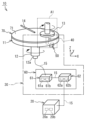
- FIG. 1 is a configuration diagram schematically showing the main configuration of a polishing apparatus according to Embodiment 1;
- FIG. 2 is a cross-sectional view near A1 in FIG. 1;
- FIG. 3 is a cross-sectional view showing a state in which the substrate holding member and the polishing table in FIG. 2 are separated;
- FIG. It is a figure which shows an example of the polishing pad in this embodiment from the direction of a polishing surface.
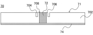
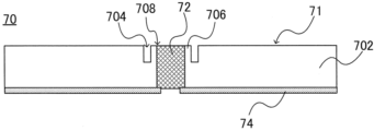
- FIG. 5 is an end view of the A5-A5 area in FIG. 4;
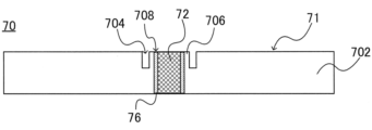
- FIG. 6 is a view corresponding to FIG. 5 in a polishing pad of a modified example;
- FIG. 6 is a view corresponding to FIG. 5 in a polishing pad of a modified example;
- FIG. 4 is a diagram showing an example of a pad block with holes; It is a figure which shows an example of the cutting process of a pad block. It is a figure which shows an example of the attachment process of a window member. It is a figure which shows an example of a pad block and a window block.
- FIG. 4 is a diagram of an example of a second layer in a pad body having two layers, viewed from the polishing surface side;
- FIG. 20 is an end view of the polishing pad with the first layer and the second layer superimposed, taken at area A20-A20 of FIGS. 18 and 19;
- FIG. 21 is a view corresponding to FIG. 20 showing an example of a polishing pad of a modified example; It is the figure which looked at an example of the 1st layer in the pad main body of the modification which has two layers from the polishing surface side.
- FIG. 24 is an end view of the modified polishing pad in which the first layer and the second layer are superimposed, taken along the line A24-A24 of FIGS. 22 and 23; It is a figure for demonstrating the manufacturing method of the polishing pad of a modification, and is a figure for demonstrating an example of the preparation process of a 2nd layer. It is a figure for demonstrating the manufacturing method of the polishing pad of a modification, and is a figure for demonstrating an example of the preparation process of a 2nd layer.
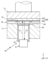
- FIG. 4 is a diagram showing an example of a polishing pad in which a window member is held movably in the penetrating direction of a through hole with respect to the pad body;
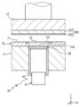
- FIG. 4 is a diagram showing an example of a polishing pad in which a window member is held movably in the penetrating direction of a through hole with respect to the pad body;
- FIG. 4 is a diagram showing an example of a polishing pad in which a window member is held movably in the penetrating direction of a through hole with respect to the pad body;
- a polishing pad, a substrate polishing apparatus (polishing apparatus), and a method for manufacturing a polishing pad according to embodiments of the present invention will be described below with reference to the drawings.
- the drawings of the present application are schematically illustrated to facilitate understanding of the features of the present embodiment, and the dimensional ratios and the like of each component are not necessarily the same as the actual ones.
- XYZ orthogonal coordinates are illustrated for reference. Of these orthogonal coordinates, the Z direction corresponds to the upward direction, and the -Z direction corresponds to the downward direction (the direction in which gravity acts).
- FIG. 1 is a configuration diagram schematically showing the main configuration of a polishing apparatus 10 according to this embodiment.
- the polishing apparatus 10 according to this embodiment is a polishing apparatus capable of performing chemical mechanical polishing (CMP). Specifically, the polishing apparatus 10 exemplified in FIG. and
- the polishing table 11 is a polishing table that holds the polishing pad 70 and is configured to rotate.
- the polishing table 11 according to this embodiment is configured by a disk-shaped member, and a polishing pad 70 is attached to the upper surface of the polishing table 11 .
- the upper surface (surface) of the polishing pad 70 corresponds to a polishing surface 71 for polishing the film of the substrate.
- the specific type of the polishing pad 70 is not particularly limited, and various polishing pads such as a hard foam type polishing pad, a non-woven fabric type polishing pad, and a suede type polishing pad can be used.
- the polishing pad 70 is appropriately set according to the type of film on the substrate to be polished.
- the polishing table 11 is connected to the rotating shaft 12 .
- the rotary shaft 12 is rotationally driven by a drive mechanism (for example, a motor or the like).
- a joint 12a is provided at the end of the rotating shaft 12 opposite to the polishing table 11 side. This joint 12a has a rotary joint and a rotary connector.
- a polishing controller 20 controls the rotation of the polishing table 11 .
- the substrate holding member 13 is arranged on the polishing surface 71 of the polishing table 11 during polishing.
- a substrate (not shown in FIG. 1) is attached to the lower surface of the substrate holding member 13 .
- the substrate holding member 13 is configured to hold the substrate and rotate while pressing the film of the substrate against the polishing surface 71 of the polishing pad 70 .
- this substrate holding member 13 is generally called a "top ring", a “polishing head”, or the like in some cases.
- the slurry supply nozzle 14 is a nozzle that supplies slurry (specifically, polishing slurry) to the polishing surface 71 .
- the slurry is, for example, a solution containing abrasive grains such as silicon oxide, aluminum oxide, and cerium oxide.
- the specific type of this slurry is not particularly limited, and may be appropriately set according to the type of film on the substrate.
- the slurry may be supplied from the lower portion of the polishing surface 71 instead of the upper portion, or may be supplied from both the upper portion and the lower portion of the polishing surface 71 .
- a channel (not shown) extending vertically from a portion near the center of rotation at the bottom of the polishing table 11 and an opening in the polishing pad 70 (polishing surface 71) communicating with the channel (not shown) are provided. (not shown) to supply the slurry.
- the polishing control device 20 is a control device that controls the operation of the polishing device 10 .
- the polishing control device 20 includes a computer.
- This computer includes a CPU (Central Processing Unit) 20a as a processor, a storage device 20b, and the like.
- the storage device 20b is composed of storage media such as ROM (Read Only Memory) and RAM (Random Access Memory).
- the CPU 20a as a processor controls the rotation of the polishing table 11, the slurry supply operation from the slurry supply nozzle 14, etc. based on the program stored in the storage device 20b. It controls the operation of the polishing apparatus 10 .
- the film thickness measurement device 30 is an optical film thickness measurement device having an optical sensor that optically measures data relating to the thickness (film thickness) of the substrate film. Further, the film thickness measurement device 30 according to the present embodiment measures data regarding film thickness during polishing by the polishing device 10 .
- the film thickness measurement device 30 includes a sensor module 40 , a light source/spectroscopic module 50 , and a data processing system 60 .
- the light source/spectroscopic module 50 , the data processing system 60 , and the polishing control device 20 are electrically connected via wiring 15 .
- the sensor module 40 and the light source/spectroscopic module 50 are arranged on the polishing table 11 .
- the sensor module 40 and the light source/spectroscopic module 50 rotate together with the polishing table 11 when the polishing table 11 rotates.
- FIG. 2 is a cross-sectional view near A1 in FIG.
- FIG. 3 is a sectional view showing a state in which the substrate holding member 13 and the polishing table 11 of FIG. 2 are separated.
- part of the polishing pad 70 according to the present embodiment has a window member 72 through which the incident light L1 and the reflected light L2 (sensing light) from the film thickness measuring device 30 can pass. are placed.
- the window member 72 is made of a light transmissive material, specifically a transparent material (for example, transparent plastic or transparent glass).
- the window member 72 is positioned so that at least a portion of the film 202 of the substrate 200 passes over the window member 72 when the polishing table 11 rotates and the polishing pad 70 rotates. position) is set.
- the window member 72 may be provided with a scattering suppression layer 72f (see FIG. 3) for suppressing scattering of sensing light.
- the scattering suppression layer 72f is preferably provided on the lower surface of the window member 72.
- a scattering suppression layer may be provided on the upper surface of the window member 72 (the surface on the substrate 200 side).
- the optical thickness of the anti-scattering layer is preferably smaller than the wavelength of light incident on the anti-scattering layer (the wavelength of sensing light from the film thickness measuring device 30). It is preferably one-fold.
- the refractive index of the scattering suppression layer is preferably smaller than the refractive index of the substance (film 202, jig 42, window member 72) adjacent to the scattering suppression layer.
- the refractive index of the scattering suppression layer is preferably, for example, the half power (square root) of (refractive index of air ⁇ refractive index of window member).
- the refractive index of the scattering suppression layer is preferably, for example, (the refractive index of the window member ⁇ the refractive index of the slurry) to the 1/2 power.
- the scattering suppression layer may be provided on the window member 72 by a known method, and for example, roll coating, gravure coating, spin coating, spraying, vacuum deposition, sputtering, or CVD is employed to form a film. can be
- the sensor module 40 of the film thickness measuring device 30 includes a sensor head 41 and a tubular jig 42.
- a jig 42 is a jig for attaching the sensor head 41 to the polishing table 11 .
- the jig 42 is connected to the polishing table 11 so that the incident light L1 and the reflected light L2 pass through the interior of the jig 42 .
- the jig 42 according to the present embodiment is fitted in a cylindrical hole provided in the polishing table 11 .
- the upper end surface of the jig 42 according to this embodiment is connected to the lower surface of the glass plate 46 arranged on the lower surface of the light transmitting member 72 .
- the incident light L1 and the reflected light L2 pass through the inside of the jig 42 (inside the cylinder).
- the glass plate 46 is configured by a plate member made of glass that transmits light, and is connected to the lower surface of the light transmission member 72 .
- the upper end surface of the jig 42 according to this embodiment (the open upper end surface of the tubular jig 42 ) is connected to the lower surface of the glass plate 46 .
- the glass plate 46 effectively prevents foreign matter such as slurry from entering the inside of the jig 42 (inside the cylinder). It is preferable that the jig 42 is in close contact with the lower surface of the glass plate 46 so that no gap is formed between the jig 42 and the glass plate 46 .
- the invention is not limited to such an example, and a gap may be provided between the jig 42 and the glass plate 46 .
- the sensor module 40 is not limited to having the glass plate 46 and may not have the glass plate 46 .
- the sensor head 41 is configured to project the incident light L1 toward the film 202 while the film 202 is being polished by the polishing apparatus 10 .
- Incident light L1 from the sensor head 41 passes through the window member 72 of the polishing pad 70 and then enters the film 202 .
- the type of light source in the sensor head 41 is not particularly limited, and a halogen lamp, a laser light emitting device, or the like can be used.
- a laser light emitting device is used as an example of the light source.
- the light emitted by the light source has a wavelength in the infrared region (specifically, a wavelength longer than 780 nm). That is, the incident light L1 according to this embodiment is laser light having a wavelength in the infrared region.
- the reflected light L2 reflected from the film 202 is received by the sensor head 41 after passing through the window member 72 .
- the sensor head 41 converts the received reflected light L2 into a digital signal and transmits the digital signal to the data processing system 60 (FIG. 1) via the wiring 15 .
- the data processing system 60 is a system that measures data regarding the film thickness of the film 202 based on the intensity of the reflected light L2 received by the sensor head 41 .
- the intensity of the reflected light L2 received by the sensor head 41 has a correlation with the film thickness. Therefore, the data processing system 60 measures data regarding the film thickness of the film 202 based on the intensity of the received reflected light L2.
- the reflected light L2 received by the sensor head 41 is spectroscopically separated by the light source/spectroscopy module 50, and the resulting spectral wave is frequency-analyzed to measure film pressure data.
- the "data relating to the film thickness” may be data having a correlation with the film thickness ( ⁇ m). (for example, the amount of change in film thickness, etc.) may be used.
- a data processing system 60 includes a first data processing device 61 and a second data processing device 62 .
- the first data processing device 61 has a computer, and this computer has a CPU 61a as a processor, a storage device 61b, and the like.
- the storage device 61b is composed of storage media such as ROM and RAM.
- the first data processing device 61 executes data processing for indexing the reflection intensity based on the data transmitted from the light source/spectroscopic module 50 by the CPU 61a operating based on the program stored in the storage device 61b. do.
- the data processed by the first data processing device 61 is transmitted to the second data processing device 62 .
- the second data processing device 62 has a computer, and this computer has a CPU 62a as a processor, a storage device 62b, and the like.
- the storage device 62b is composed of storage media such as ROM and RAM.
- the second data processing device 62 executes noise removal processing of the time waveform of the indexed data by the operation of the CPU 62a based on the program stored in the storage device 62b, and the noise removal processing is executed. After that, the waveform is analyzed to detect reflection intensity and feature points (feature points such as maximum and minimum values of differential values and threshold values). This detected value (detected value) has a correlation with the film thickness. Therefore, the second data processing unit 62 calculates and acquires data regarding the film thickness based on this detected value. As described above, the data processing system 60 according to the present embodiment measures data on film thickness.
- the second data processing device 62 determines whether the film thickness has reached a preset polishing end point (that is, the polishing end point of polishing) based on the data measured as described above. ). When determining that the film thickness has reached the polishing end point, the second data processing device 62 transmits a signal (polishing end point signal) to the effect that the polishing end point has been reached to the polishing control device 20 . Upon receiving this polishing end point signal, the polishing control device 20 stops the driving mechanism (for example, the motor) of the polishing device 10 to end the polishing by the polishing device 10 .
- a preset polishing end point that is, the polishing end point of polishing
- the data processing algorithm by the data processing system 60 described above (that is, the data processing algorithm for measuring the data related to the film thickness based on the intensity of the reflected light) is disclosed in the above-mentioned Patent Document 1 and Patent Document 2. It is the same as a data processing device used in a known film thickness measuring device such as the one described above, and these techniques can be applied. Therefore, a more detailed description of this data processing is omitted.
- FIGS. 2 and 3 described above show an example of the mounting manner of the sensor head 41 to the polishing table 11, and the mounting manner of the sensor head 41 to the polishing table 11 is illustrated in FIGS. It is not limited to the mode.
- the polishing apparatus 10 as described above polishes the film of the substrate held by the substrate holding member 13 to a desired flat surface by rotating the polishing table 11 and the substrate holding member 13 in the presence of slurry.
- the film thickness of the film 202 on the substrate 200 can be measured by the film thickness measuring device 30, and the polishing device 10 determines the time when the film thickness of the substrate reaches a preset value as the polishing end point ( That is, it is referred to as "polishing end point").
- the specific value of the polishing end point is not particularly limited.
- the polishing end point may be a value equal to or less than the film thickness at which a wiring pattern (not shown) buried in the film is exposed on the surface of the film before polishing.
- a value larger than the film thickness at which the wiring pattern is exposed on the surface of the film may be set as the polishing end point.
- FIG. 4 is a view showing an example of the polishing pad in this embodiment from the direction of the polishing surface
- FIG. 5 is an end view of the A5-A5 area in FIG.
- the polishing pad 70 of the present embodiment includes a pad body 702 having a polishing surface 71, a window member 72 for transmitting sensing light from the film thickness measuring device 30, and an adhesive layer 74 attached to the back surface of the pad body 702 .
- the adhesive layer 74 functions as a holding mechanism for holding the polishing pad 70 on the polishing table 11 .
- a double-sided tape or an adhesive for example, a hot melt adhesive or a UV curable adhesive
- an adhesive for example, a hot melt adhesive or a UV curable adhesive
- the double-sided tape for example, an airtight PET (polyethylene terephthalate) film-like base material coated with an adhesive on both sides is preferable.
- a through hole 708 for accommodating the window member 72 is formed in the pad body 702 .
- the through-hole 708 preferably has a shape corresponding to the window member 72 when viewed from the polished surface 71 , and has the same size as the window member 72 or a slightly larger size so that there is a gap between the through hole 708 and the window member 72 .
- the through hole 708 preferably has a depth smaller than the height of the window member 72 or the same depth as the height of the window member 72 . In other words, it is preferable that the pad body 702 and the window member 72 have the same height, or the height of the window member 72 is slightly larger than the height of the pad body 702 .
- the window member 72 By making the height of the window member 72 slightly larger than the height of the pad main body 702, it is possible to prevent the window member 72 from recessing from the surface of the pad main body 702 due to manufacturing variations or the like. Thereby, it is possible to suppress the slurry from remaining on the surface of the window member 72 .
- the window member 72 may be formed by filling the through holes 708 of the pad body 702 with a fluid material.
- the window member 72 may be attached to the pad body 702 with an adhesive layer.
- the window member 72 is attached to the pad body 702 by an adhesive layer 74 that is applied to the back surface of the pad body 702 and holds the polishing pad 70 to the polishing table 11 .
- an adhesive layer 74 is applied over the entire back surface of the window member 72 (the surface opposite to the polished surface 71 side).
- An opening may be formed in the adhesive layer 74 .
- the window member 72 may be attached to the pad main body 702 by attaching an adhesive layer 74 to the edge of the window member 72 on the outer peripheral side of the translucent region.
- the window member 72 is attached to the pad body 702 by the adhesive layer 74 attached to the back surface of the pad body 702. It may be attached to the pad body 702 by an adhesive layer 76 interposed between the pad body 702 and the through holes 708 .
- illustration of the adhesive layer 74 attached to the back surface of the pad body 702 is omitted.
- the window member 72 is formed so as to contact the wall surface (edge portion 706) defining the through hole 708 of the pad body 702, that is, so that a gap is not formed between the pad body 702 and the window member 72. may be accommodated in Also, as described above, the through-hole 708 may have a size larger than the window member 72 so as to have a gap (for example, several millimeters) with the window member 72 .
- FIG. 8 is a diagram showing an example of a modified polishing pad. As shown in FIG. 8, the permissible range of dimensional tolerance of the window member 72 is increased by making the through hole 708 larger than the window member 72 so that a gap 712 is formed between the through hole 708 and the window member 72 . You can make it bigger.
- the window member 72 can be easily accommodated in the through hole 708 and attached to the pad body 702 . Thereby, even after the pad main body 702 is attached to the polishing table 11 , the window member 72 can be easily attached in the through hole 708 .
- the adhesive layer 74 is applied over the entire rear surface of the window member 72. However, as in the example shown in FIG. Additionally, an opening may be formed in the adhesive layer 74 .
- the window member 72 has a cylindrical shape.
- the window member 72 is not limited to such an example, and may have a polygonal shape, an elliptical shape, or the like when viewed from the direction perpendicular to the polishing surface 71 .
- the window member 72 may have an attachment edge 72a for attachment to the pad body 702, as shown in the modified example of FIG.
- the attachment edge portion 72 a is an edge portion that protrudes from the outer periphery of the window member 72 , and may be provided over the entire outer periphery of the window member 72 or only part of the outer periphery of the window member 72 .
- the through hole 708 of the pad body 702 is preferably formed to have a stepped portion on which the mounting edge portion 72a is placed. Further, as an example, an adhesive layer 78 may be provided between the lower surface of the attachment edge portion 72 a and the stepped portion of the through hole 708 .
- the pad body 702 is formed with a surrounding recess 704 surrounding an edge 706 defining a through hole 708 .
- Surrounding recess 704 is recessed from polishing surface 71 relative to edge 706 .
- the edge 706 has the same height as the polishing surface 71, and the surrounding recess 704 is a recess with a height lower than that of the polishing surface 71.
- the surrounding recess 704 communicates with a groove 710 extending on the outer peripheral surface of the polishing pad 70 . In the example shown in FIGS. 4 and 5, two grooves 710 communicate with the surrounding recess 704 .
- These two grooves 710 are grooves that are open to the polishing surface 71 and extend so as to connect the surrounding recess 704 and the outer periphery of the pad body 702 .
- the surrounding recess 704 or the groove 710 can have a width of several millimeters or several tens of millimeters, for example.
- the surrounding recess 704 or the groove 710 can have a depth of several millimeters or several tens of millimeters, for example. 4 and 5, the surrounding recess 704 and the groove 710 have the same width and depth.
- groove 710 may have a greater depth than surrounding recess 704 . It should be noted that the groove 710 is not limited to the example shown in FIG.
- the polishing slurry supplied to the polishing surface 71 during polishing is discharged from the surrounding recess 704 through the grooves 710, thereby suppressing the slurry from going to the surface of the window member 72. be able to.
- the sensing light from the film thickness measuring device 30 it is possible to prevent the sensing light from the film thickness measuring device 30 from being blocked by the polishing slurry adhering to the surface of the window member 72 and lowering the measurement accuracy of the film thickness measuring device 30 . Therefore, it is possible to improve the detection accuracy of the film thickness of the substrate 200 by the film thickness measuring device 30 having the optical sensor.
- the polishing slurry flows into the gap between the through-hole 708 and the window member 72, so that the surface of the window member 72 is It is possible to suppress the slurry from going to. Therefore, if there is a gap between the through hole 708 and the window member 72, the polishing pad 70 may not have the surrounding recess 704 and the groove 710 described above.
- FIG. 10 is a diagram corresponding to FIG. 4 showing an example of a polishing pad of a modification.
- the polishing pad 70 shown in FIG. 4 has two grooves 710 .
- the polishing pad 70A (pad main body 702A) shown in FIG. Grid-shaped grooves 710A extend to the outer peripheral surface of polishing pad 70A.
- the pad main body 702A is formed with a through hole 708 for accommodating the window member 72 in the same manner as the polishing pad 70 described above, and is surrounded by an edge portion 706A defining the through hole 708.
- a recess 704A is formed.
- the groove 710A and the surrounding recess 704A are in communication.
- the grid-shaped grooves 710A and the surrounding recesses 704A may have the same depth, or the grid-shaped grooves 710A may have a greater or lesser depth than the surrounding recesses 704A. Also in the polishing pad 70A of this modification, the surrounding recess 704A communicates with the grid-like grooves 710A extending on the outer peripheral surface of the polishing pad 70A, and the same effect as the polishing pad 70 described above can be achieved.
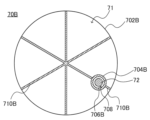
- FIG. 11 is a diagram corresponding to FIG. 4 showing an example of a polishing pad of a modification.
- a plurality of radial grooves 710B extending from the center of the polishing surface 71 toward the outer periphery are formed in the polishing pad 70B (pad main body 702B) shown in FIG. Further, the pad main body 702B is formed with a through hole 708 for accommodating the window member 72 in the same manner as the polishing pads 70 and 70A described above. is formed with a surrounding recess 704B.
- the groove 710B and the surrounding recess 704B are in communication.
- the radial grooves 710B and the surrounding recesses 704B may have the same depth, or the radial grooves 710B may have a greater or lesser depth than the surrounding recesses 704B.
- the surrounding recess 704B communicates with the grid-like grooves 710B extending on the outer peripheral surface of the polishing pad 70B, and the same effects as those of the polishing pads 70 and 70A can be obtained. can.
- radial grooves 710B extending linearly from the center of the polishing surface 71 toward the outer periphery are formed. or a plurality of concentric circular grooves having different radii with respect to the center of rotation of the polishing surface 71 (or a certain position in the vicinity thereof), or the grooves are formed with each other. may be appropriately combined so as to communicate with each other.
- the pad body 702 is prepared.
- the pad body 702 is formed, for example, from the pad block 130 as the material of the plurality of pad bodies 702 .
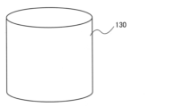
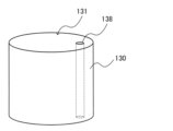
- FIG. 12 is a perspective view showing an example of the pad block 130 of this embodiment.
- the pad block 130 has a generally columnar shape and is cut into a plurality of pad bodies 702 . In other words, the pad block 130 corresponds to a stack of a plurality of pad bodies 702 .
- FIG. 13 shows an example of a pad block 130 having holes 138 formed therein. As shown in FIG. 13, a hole 138 is formed in the direction perpendicular to the surface 131 forming the polishing surface 71 of the pad body 702 in the pad block 130 (vertical direction in FIGS. 12 and 13). Holes 138 may be formed by known methods.
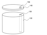
- FIG. 14 is a diagram showing an example of a pad block cutting process
- FIG. 15 is a diagram showing an example of a window member mounting process.
- the pads 140 that form the base of the pad body 702 are formed.
- Holes 138 formed in pad block 130 define through holes 708 for receiving window members 72 in cut pads 140 .
- the polishing pad 70 is manufactured by attaching the window member 72 to the pad 140 and forming the surrounding recess 704 and the groove 710 in the pad 140 (not shown in FIG. 15).
- the surrounding recess 704 and the groove 710 may be formed in the pad block 130 before cutting the pad block 130, may be formed in the pad 140 before attaching the window member 72, or may be formed in the pad 140 before the window member 72 is attached. It may be formed into the pad 140 after it is attached. Further, in the example shown in FIGS. 13 to 15, the hole 138 is formed in the pad block 130, but the present invention is not limited to such an example, and the through hole 708 is formed in the pad 140 separated from the pad block 130. may be formed.
- the window member 72 may be a pre-formed window member 72 attached to the through holes 708 of the pad 140, or may be constructed by filling the through holes 708 with a fluid material.
- a mold whose surface roughness is controlled may be used. In this way, the manufacturing roughness of the window member 72 to be manufactured can be controlled, and the detection accuracy of the film thickness measuring device 30 in the polishing apparatus can be improved.
- the window member 72 may be subjected to surface roughness improvement treatment before or after being attached to the through hole 708 of the pad 140 .
- the window member 72 may be subjected to surface roughness improvement treatment by cutting or polishing the surface.
- the window member 72 has a lower surface (a surface farther from the substrate 200) processed to have a predetermined surface roughness or less. This is based on the fact that the lower surface of the window member 72 is unlikely to be worn or damaged by the polishing process by the polishing apparatus 10 and the dressing of the polishing pad 70 .
- the lower surface of the window member 72 is preferably subjected to surface roughness improvement treatment so as to have PV (maximum valley depth: JIS B 0601) of 0.5 ⁇ m or less, for example. It is more preferable that surface roughness improvement treatment is applied so as to have the following PV.
- the window member 72 is attached to the pad 140 cut off from the pad block 130 .
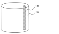
- the invention is not limited to such an example, and as an example, a window block 132 constituting a plurality of window members 72 is arranged in a hole 138 of the pad block 130, and the pad block 130 and the window block 132 are cut to form a pad 140. and a window member 72 may be formed.
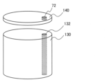
- FIG. 16 is a diagram showing an example of a pad block and a window block
- FIG. 17 is a diagram showing an example of a cutting process of the pad block and the window block.
- the window block 132 may be a pre-formed window block 132 attached to the hole 138 of the pad block 130 or constructed by filling the hole 138 with a fluid material. good too.
- the pad blocks 130 forming the plurality of pad bodies 702 are prepared, but the present invention is not limited to this example.
- the pad 140 constituting one pad body 702 is molded, and the pad 140 is formed with the through hole 708, the surrounding recess 704, and the groove 710, and the window member 72 is provided in the through hole 708.
- the polishing pad 70 may be manufactured.
- the pad 140 having at least one of the through hole 708, the surrounding recess 704, and the groove 710 formed in advance may be molded, and the polishing pad 70 may be manufactured using the pad 140.
- the pad body 702 is formed of a single layer.
- the pad body 702 of the polishing pad 70 may be formed of multiple layers.
- the pad body 702 of the polishing pad 70 described above includes a pad layer in which through holes are formed that define the side surfaces of the surrounding recess 704 and the groove 710, and a pad layer that defines the bottom surface of the surrounding recess 704 and the groove 710. and may be laminated.
- the pad body 702 may be composed of a plurality of layers formed of the same material, or may be composed of a plurality of layers of different materials.
- the pad body 702 may be configured by stacking.
- FIG. 18 is a view of an example of a first layer in a pad body having two layers viewed from the polishing surface side
- FIG. 19 is a view of an example of a second layer in a pad body having two layers viewed from the polishing surface side. It is a view.
- FIG. 20 is an end view of the polishing pad in which the first layer and the second layer are superimposed, taken along the line A20-A20 of FIGS. 18 and 19.
- the polishing pad 170 shown in FIGS. 18-20 has a first layer (first pad layer) 171 and a second layer (second pad layer) 172 .
- the first layer 171 constitutes a polishing surface 173 whose surface contacts the substrate 200 .
- the second layer 172 is laminated on the back surface of the first layer 171 (the surface opposite to the polished surface 173).
- the polishing pad 170 has two layers, the first layer 171 and the second layer 172, the present invention is not limited to this example, and as an example, at least one of the first layer 171 and the second layer 172 may be composed of multiple layers.
- the second layer 172 of the polishing pad 170 is formed with a through hole 1728 in which a portion of the window member 72 is accommodated.
- a through hole 1718 is formed in the first layer 171 of the polishing pad 170 to accommodate a portion of the window member 72 .
- the through-hole 1718 of the first layer 171 preferably has a dimension larger than that of the through-hole 1728 of the second layer 172 .
- the through-hole 1718 of the first layer 171 preferably has the same size as the surrounding recessed portion 1724 of the second layer 172 described later, or has a larger size than the surrounding recessed portion 1724 .
- grooves 1710 are formed in the polishing surface 173 of the first layer 171 .
- the grooves 1710 are mainly provided so that the polishing slurry is evenly supplied to the polishing surface 173 .
- the grooves 1710 are provided in a grid pattern over the entire polishing surface 173 .
- the first layer 171 is not limited to such an example, and the first layer 171 may be provided with, for example, radial grooves as shown in FIG. or a plurality of concentric circular grooves having different radii with respect to the center of rotation of the polishing surface 173 (or a certain position in the vicinity thereof), or the grooves are formed with each other. may be appropriately combined so as to communicate with each other, or such grooves may not be formed.
- a surrounding recess 1724 is formed in the second layer 172 so as to surround an edge 1726 defining a through hole 1728 .
- Surrounding recess 1724 is recessed relative to polishing surface 173 relative to edge 1726 .
- the edge portion 1726 has the same height as the surface of the second layer 172 that contacts the back surface of the first layer 171
- the surrounding recess 1724 has the same height as the back surface of the first layer 171.
- the height of the concave portion is lower than that of the concave portion.
- a groove 1729 is formed in the second layer 172 to communicate with the surrounding recess 1724 and extend to the outer peripheral surface of the polishing pad 170 .
- two grooves 1729 communicate with the surrounding recess 1724 .
- the groove 1729 is not limited to the example shown in FIG. 19 as long as the groove 1729 communicates between the surrounding recess 1724 and the outer peripheral surface of the polishing pad 170 .
- no through holes are formed in the first layer 171 at the positions of the grooves 1729 in the second layer 172 . Therefore, in the polishing pad 170 in which the first layer 171 and the second layer 172 are laminated, the grooves 1729 of the second layer 172 are covered with the first layer 171 .
- the through holes 1718 of the first layer 171 are larger than the surrounding recesses 1724 of the second layer 172.
- the through hole 1728 of the second layer 172 is formed to have a dimension larger than that of the window member 72 so that a gap is formed between the through hole 1728 and the window member 72 .
- the through hole 1728 of the second layer 172 may have the same dimensions as the window member 72 when viewed from the direction perpendicular to the polishing surface 173 .
- the window member 72 has substantially the same height as the combined height of the first layer 171 and the second layer 172 .
- the window member 72 may have a height slightly greater than the combined height of the first layer 171 and the second layer 172 . 18 to 20, an adhesive layer 174 for bonding the first layer 171 and the second layer 172 is formed on the back surface of the first layer 171.
- an adhesive layer 174 for bonding the first layer 171 and the second layer 172 is formed on the back surface of the first layer 171.
- the polishing slurry supplied to the polishing surface 173 during polishing is discharged from the surrounding recesses 1724 of the second layer 172 through the grooves 1729, so that the slurry is directed to the surface of the window member 72. can be suppressed.
- an adhesive layer 174 for bonding the first layer 171 and the second layer 172 together is provided on the back surface of the first layer 171 .
- the adhesive layer 174 may be provided on the upper surface of the second layer 172 .
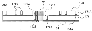
- FIG. 21 is a diagram corresponding to FIG. 20 showing an example of a polishing pad 170A of a modified example.
- the window member 72 and the second layer 172 may be fixed using the adhesive layer 174 on the upper surface of the edge portion 1726 .
- the window member 72 may have a mounting edge 72 a and the window member 72 may be secured to the second layer 172 by resting the mounting edge 72 a on top of the edge 1726 .
- FIG. 22 is a diagram of an example of the first layer in a modification of the pad body having two layers, viewed from the polishing surface side
- FIG. 23 is a diagram of the second layer in the modification of the pad body having two layers. It is the figure which looked at an example from the polishing surface side.
- FIG. 24 is an end view of the modified polishing pad in which the first layer and the second layer are superimposed, taken along the line A24-A24 of FIGS. 22 and 23.
- FIG. A polishing pad 170A shown in FIGS. 22-24 has a first layer 171A and a second layer 172. As shown in FIG. The surface of the first layer 171A constitutes a polished surface 173A.
- the second layer 172 is laminated on the back surface of the first layer 171 (the surface opposite to the polished surface 173) via an adhesive layer 174A.
- the second layer 172 is the same as the second layer 172 shown in FIG.
- the first layer 171A shown in FIG. 22 is substantially the same as the first layer 171 shown in FIG. 18, and the same components as those of the first layer 171 shown in FIG. omitted. As shown in FIGS. 22 and 24 , the first layer 171 ⁇ /b>A of the modified example is provided with an edge portion 1716 corresponding to the edge portion 1726 of the second layer 172 . The edge 1716 of the first layer 171A is separated from the through hole 1718 of the first layer 171A.
- the polishing pad 170A of such a modified example can also achieve the same effects as the polishing pad 170 described above.
- a pad 182 as a material for the second layer 172 is prepared.
- the pads 182 may be prepared by cutting a pad block, such as the pad block 130 described above, that constitutes a plurality of second layers 172, or the pads 182 that constitute a single second layer 172 may be prepared. may be prepared by molding.
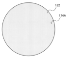
- an adhesive layer 174A is provided on the upper surface of the prepared pad 182 (the surface that contacts the first layer 171A).
- the adhesive layer 174A for example, a double-sided tape or an adhesive (eg, hot melt adhesive, UV curing adhesive) can be used.
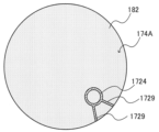
- the second layer 172 is prepared by forming a surrounding recess 1724 and a groove 1729 in the upper surface of the pad 182 .
- the surrounding recess 1724 and the groove 1729 may be formed by a known processing method.
- the surface of the pad 182 may be masked where the surrounding recess 1724 and the groove 1729 are to be formed.
- the adhesive layer 174A may be marked or notched where the surrounding recesses 1724 and grooves 1729 are to be formed. This facilitates formation of the surrounding recess 1724 and the groove 1729 in the pad 182 .
- a process of preparing the first layer 171A for manufacturing the polishing pad 170A will be described.
- 28 and 29 are diagrams for explaining an example of the preparation process of the first layer.
- the preparation process of the first layer 171A will be described after the preparation process of the second layer 172, but the second layer 172 may be prepared after the first layer 171A is prepared, At least part of the preparation process of the layer 171A and the preparation process of the second layer 172 may be performed in parallel.
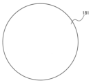
- a pad 181 is prepared as a material for the first layer 171A.
- the pad 181 may be prepared by cutting a pad block, similarly to the pad 182 as the material of the second layer 172, or may be prepared by molding one pad.
- a first layer 171A is prepared by forming a cut 181a in the pad 181 to define a through hole 1718 and an edge 1716.
- the pad 181 is physically divided into a plurality of parts by the formed cuts 181a, but the parts where the cuts 181a are formed are not removed and left as they are.
- FIG. 30 shows an example of a laminate of the second layer shown in FIG. 27 and the first layer shown in FIG.
- the prepared first layer 171A and second layer 172 are laminated and adhered by an adhesive layer 174A.
- a through hole 1718 is formed in the first layer 171A by removing the portion separated by the cut 181a that defines the through hole 1718 and the edge 1716 in this state.
- the edge 1716 provided inside the through-hole 1718 of the first layer 171A and the edge 1726 of the second layer 172 can be easily aligned.
- a through-hole 1728 is formed in the laminate of the first layer 171A and the second layer 172, and a window member 72 is attached to the formed through-hole 1728, thereby having two layers.
- a polishing pad 170A is manufactured.
- the through hole 1728 is a hole penetrating the first layer 171A and the second layer 172, and may be formed by a known processing method. In this way, after laminating the first layer 171A and the second layer 172, the through-hole 1728 that penetrates the first layer 171A and the second layer 172 is formed. can be easily formed.
- the attachment of the window member 72 to the through-hole 1728 may be performed by attaching a previously formed window member 72 to the through-hole 1728 in the same manner as described in the manufacturing method of the single-layer polishing pad 70 .
- the through-hole 1728 may be filled with a fluid material. If the window member 72 has the mounting edge 72a, the pad 140 may be provided with a step corresponding to the mounting edge 72a.
- the first layer (171, etc.) that is the upper layer including the polishing layer having the polishing surface 173 and the second layer (172, etc.) that is the lower layer including the support layer are made of the same material. but can be different.
- the first layer may be set harder than the second layer depending on the material of the substrate 200 and the quality of the film to be polished.
- the window member 72 is fixed to the pad main body 702 by the adhesive layer so as to be substantially immovable.
- the window member 72 may be held movably with respect to the pad body 702 without being limited to such an example.
- the window member 72 may be configured to be movable in the penetrating direction of the through hole 708 with respect to the pad body 702 .
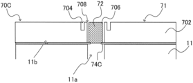
- FIGS. 32-34 are diagrams showing an example of a polishing pad in which a window member is held movably in the penetrating direction of the through-hole with respect to the pad body.
- 32 to 34 show the polishing pad 70C placed on the polishing table 11.
- polishing pad 70C is not limited to having the same shape as polishing pad 70, and may not have surrounding recess 704 or groove 710, or other grooves may be formed in polishing surface 71. .
- the adhesive layer 74C is provided on the back surface of the polishing pad 70C (the surface opposite to the polishing surface 71). It may be provided so as to be interposed between the member 72 and the through hole 708 of the pad body 702 .
- the adhesive layer 74C corresponds to an example of a holding member for movably holding the window member 72 on the pad body 702. As shown in FIG.
- the polishing pad 70C may include another holding member that movably holds the window member 72 with respect to the pad body 702 instead of or in addition to the adhesive layer 74C.
- the adhesive layer 74C for example, a double-sided tape in which an adhesive is applied to both sides of an airtight PET (polyethylene terephthalate) film base material can be used, but the adhesive layer 74C is not limited to such an example.
- the polishing table 11 is formed with an opening 11a into which the window member 72 can enter. That is, the polishing table 11 has a support surface 11b for supporting the back surface (lower surface) of the pad body 702, and the opening 11a is formed in the support surface 11b.
- the opening 11a preferably has a shape corresponding to the shape of the window member 72 (shape in a plane parallel to the polishing surface of the polishing pad 70C). It is preferable to have a shape larger than the window member 72 by a predetermined dimension so as to have a gap. In the example shown in FIGS. 32 to 34, the opening 11a is not provided with the glass plate 46 shown in FIGS.
- the glass plate 46 may be installed (below the support surface 11b) so as to provide a gap between the lower surface of the window member 72 and the glass plate 46 so that they do not come into contact with each other.
- the polishing pad 70C is not a single-layer polishing pad, and a laminated polishing pad having two or more layers as described above provided with an adhesive layer 74C may be applied.
- the heights of the window member 72 and the pad body 702 are substantially the same. Therefore, when the polishing pad 70C is newly provided on the polishing table 11, as shown in FIG. 32, the polishing surface 71 and the upper surface of the window member 72 are substantially flush (constitute the same plane).
- the polishing pad 70C is used in the polishing process, it can be assumed that the pad main body 702 is consumed and the height of the pad main body 702 is reduced as shown in FIG. Even in such a case, as shown in FIG. 34, the substrate 200 held by the substrate holding member 13 is pressed against the polishing pad 70C during polishing, so that the window member 72 is pressed and the opening 11a of the polishing table 11 is closed.
- the window member 72 is not limited to being configured to have approximately the same height as the pad main body 702, and may be configured to have a height slightly greater than the height of the pad main body 702. . 34, the substrate 200 held by the substrate holding member 13 is pressed against the polishing pad 70C during polishing, so that the window member 72 is pressed and the polishing table 11 is displaced. By entering the opening 11a, the height relationship between the polishing surface 71 of the pad body 702 and the upper surface of the window member 72 can be maintained.
- mode 1 there is proposed a polishing pad for a substrate polishing apparatus equipped with an optical sensor. and a window member for passing the sensing light of the optical sensor, the window member being accommodated in the through hole, wherein the pad main body has an edge defining the through hole. It has a surrounding recess that is recessed relative to the polishing surface relative to the edge, and the surrounding recess communicates with a groove extending to the outer peripheral surface of the polishing pad.
- the first aspect it is possible to improve the detection accuracy of the optical sensor in the substrate polishing apparatus including the optical sensor for detecting the state of the substrate surface.
- Mode 2 According to Mode 2, in Mode 1, the surrounding recess and the groove have the same depth.
- Mode 3 According to Mode 3, in Mode 1 or 2, the grooves are formed in a grid pattern in the pad body.
- Mode 4 According to Mode 4, in Modes 1 to 3, the grooves are formed radially, concentrically, or spirally in the pad body.
- the pad body has a first pad layer having the polishing surface and a second pad layer laminated on the first pad layer. , the groove is formed in the second pad layer.
- Mode 6 According to mode 6, in modes 1 to 5, the window member is accommodated in the through hole so as to be in contact with the edge defining the through hole. In other words, the window member is accommodated in the through hole so that no gap is formed between the window member and the pad body.
- Mode 7 According to Mode 7, in Modes 1 to 5, the window member is accommodated in the through hole so that a gap is formed between the window member and the pad body.
- Mode 8 According to Mode 8, in Modes 1 to 7, the pad body and the window member have the same thickness, or the window member has a greater thickness than the pad body.
- Mode 9 According to Mode 9, in Modes 1 to 8, the window member is provided with a scattering suppression layer for suppressing scattering of the sensing light.
- Mode 10 According to Mode 10, in Modes 1 to 9, the surface of the pad body opposite to the polishing surface of the window member is subjected to surface roughness improvement treatment.
- Mode 11 there is proposed a substrate polishing apparatus comprising the polishing pad according to any one of Modes 1 to 10, a polishing table for mounting the polishing pad, A polishing head for holding a substrate is provided to face the polishing table, and an optical sensor is provided on the polishing table for measuring progress of polishing of the substrate. According to the eleventh aspect, it is possible to improve the detection accuracy of the optical sensor in the substrate polishing apparatus.
- Mode 12 According to Mode 12, a method for manufacturing the polishing pads of Modes 1 to 10 is proposed. forming a hole in the pad block that defines the through hole; cutting the pad block to form a pad body; and opening the through hole in the formed polishing pad. and attaching the member.
- Mode 13 According to Mode 13, a method for manufacturing the polishing pads of Modes 1 to 10 is proposed. forming a hole in the pad block that defines the through hole; placing a window block in the hole formed in the pad block; and combining the pad block and the window block. cutting to form a pad body and a window member.
- a polishing pad for attaching the polishing pad, a polishing head for holding a substrate provided so as to face the polishing table, and the polishing table. and an optical sensor for measuring the progress of polishing of the substrate.
- the polishing pad includes a pad body having a polishing surface, and a pad body having through holes formed therein, and a window member for passing sensing light from the optical sensor, wherein the through holes have It has a window member to be accommodated, and a holding member that holds the window member movably in the penetrating direction of the through hole with respect to the pad body.
- the polishing table has a support surface for supporting the back surface of the pad body, and the support surface is formed with an opening into which the window member can enter.
- the substrate polishing apparatus including the optical sensor for detecting the state of the substrate surface, damage to the substrate due to contact between the window member and the substrate can be suppressed, and damage to the window member can be suppressed. Therefore, it is possible to improve the detection accuracy of the optical sensor.
- Mode 15 According to Mode 15, in Mode 14, the polishing pad is attached to the support surface of the polishing table with an adhesive layer.
- Mode 16 According to Mode 16, in Mode 15, the holding member is the adhesive layer.
- the holding member is an airtight double-faced tape.
- Patent Document 1 JP 2010-23210 A
- Patent Document 2 JP 2001-235311 A
- Patent Document 3 JP 10-229060 A
- Patent Document 4 JP 2001-21317 A
- Patent Document 5 Japanese Patent No. 6606309
- polishing device 11 polishing table 13 substrate holding member 20 polishing control device 30 film thickness measuring device 40 sensor module 41 sensor head 42 jig 60 data processing system 70, 70A, 70B, 70C polishing pad 71 polishing surface 72 window member 72f scattering suppression Layers 74, 74C Adhesive layer 702 Pad body 704, 704A, 704B Surrounding recesses 708, 708A, 708B Through holes 710, 710A, 710B Grooves 712 Gap 170, 170A Polishing pad 171 First layer (first pad layer) 172 second layer (second pad layer) 173, 173A polished surface 1724 surrounding recess 1728 through hole 1729 groove 200 substrate 202 film L1 incident light L2 reflected light
Landscapes
- Engineering & Computer Science (AREA)
- Mechanical Engineering (AREA)
- Finish Polishing, Edge Sharpening, And Grinding By Specific Grinding Devices (AREA)
- Mechanical Treatment Of Semiconductor (AREA)
- Constituent Portions Of Griding Lathes, Driving, Sensing And Control (AREA)
Abstract
基板表面の状態を検出するための光学センサを備える基板研磨装置において、光学センサによる検出精度を向上させる。 光学センサを備える基板研磨装置のための研磨パッドが提案される。かかる研磨パッドは、表面が研磨面を構成するパッド本体であって、貫通孔が形成されているパッド本体と、前記光学センサのセンシング光を通過させるための窓部材であって、前記貫通孔に収容される窓部材と、を備え、前記パッド本体は、前記貫通孔を画定する縁部を囲繞し、前記縁部よりも前記研磨面に対して凹んだ囲繞凹部を有し、前記囲繞凹部は、前記研磨パッドの外周面に延びる溝と連通している。
Description
本発明は、研磨パッド、基板研磨装置、及び研磨パッドの製造方法に関する。
従来、基板に形成された無機絶縁膜を平坦化するために、例えば化学機械研磨(Chemical Mechanical Polishing;CMP)が行われている(例えば、特許文献1~3参照)。このような研磨に用いられる研磨装置は、研磨パッドを保持するとともに回転する研磨テーブルと、基板を保持するとともに基板の膜を研磨パッドに押し付けながら回転する基板保持部材とを備えている。そして、この研磨装置は、スラリーの存在下で研磨テーブル及び基板保持部材が回転することで、膜を研磨している。
また、従来、研磨装置による膜の研磨中に、膜厚に関するデータを光学的に測定する膜厚測定装置が知られている(例えば、特許文献1~3参照)。具体的には、このような膜厚測定装置は、研磨装置による研磨中に基板に向けて入射光を投光し、この基板から反射された反射光の強度に基づいて、膜厚に関するデータを測定している。そして、この研磨装置は、膜厚測定装置によって基板板面の膜厚に関するデータを測定しながら研磨を行い、膜厚が所定の値になったときに研磨終点に達したと判断して、研磨を終了させている。
また、従来、基板に形成された膜として、複数の配線パターンを含む膜が知られている(例えば特許文献4参照)。また、このような配線パターンを含む膜として、有機化合物によって構成された膜(すなわち、有機絶縁膜)が知られている。そして、このような有機絶縁膜の平坦化にも、CMPが行われている(例えば特許文献5参照)。
しかしながら、上記したように光学センサを用いて基板表面の状態を検出しながら基板の研磨を行う場合、基板の研磨処理に伴って光学センサによる検出に不具合が生じる場合があった。例えば、研磨装置では、スラリー存在下で研磨テーブル及び基板保持部材が回転することで基板の研磨が行われるが、スラリーによって光学センサのセンシング光が遮られ、光学センサによる検出精度が低下してしまう場合があった。また、研磨パッドに光学センサのセンシング光を通過させるための窓部材が設けられている場合、研磨処理に伴って研磨パッドが消耗することで、窓部材と基板表面との距離が変化して光学センサによる検出精度が低下してしまう場合があった。
本発明は、上記のことを鑑みてなされたものであり、基板表面の状態を検出するための光学センサを備える基板研磨装置において、光学センサによる検出精度を向上させることを目的の一つとする。
本発明の一形態によれば、光学センサを備える基板研磨装置のための研磨パッドが提案される。かかる研磨パッドは、表面が研磨面を構成するパッド本体であって、貫通孔が形成されているパッド本体と、前記光学センサのセンシング光を通過させるための窓部材であって、前記貫通孔に収容される窓部材と、を備え、前記パッド本体は、前記貫通孔を画定する縁部を囲繞し、前記縁部よりも前記研磨面に対して凹んだ囲繞凹部を有し、前記囲繞凹部は、前記研磨パッドの外周面に延びる溝と連通している。
本発明の別の一形態によれば、研磨パッドと、前記研磨パッドを取り付けるための研磨テーブルと、前記研磨テーブルに対向するように設けられた、基板を保持するための研磨ヘッドと、前記研磨テーブルに設けられた、前記基板の研磨の進行を測定するための光学センサと、を備える基板研磨装置が提案される。前記研磨パッドは、表面が研磨面を構成するパッド本体であって、貫通孔が形成されているパッド本体と、前記光学センサのセンシング光を通過させるための窓部材であって、前記貫通孔に収容される窓部材と、前記窓部材を前記パッド本体に対して前記貫通孔の貫通方向に移動可能に保持する保持部材と、を有する。前記研磨テーブルは、前記パッド本体の裏面を支持するための支持面を有し、前記支持面には、前記窓部材が進入可能な開口が形成されている。
以下、本発明の実施形態に係る研磨パッド、基板研磨装置(研磨装置)、及び研磨パッドの製造方法について、図面を参照しつつ説明する。なお、本願の図面は、本実施形態の特徴の理解を容易にするために模式的に図示されており、各構成要素の寸法比率等は実際のものと同じであるとは限らない。また、本願の図面には、参考用として、X-Y-Zの直交座標が図示されている。この直交座標のうち、Z方向は上方に相当し、-Z方向は下方(重力が作用する方向)に相当する。
図1は、本実施形態に係る研磨装置10の主要な構成を模式的に示す構成図である。本実施形態に係る研磨装置10は、化学機械研磨(Chemical Mechanical Polishing;CMP)を行うことが可能な研磨装置である。具体的には、図1に例示されている研磨装置10は、研磨テーブル11と、回転軸12と、基板保持部材13と、スラリー供給ノズル14と、研磨制御装置20と、膜厚測定装置30とを備えている。
研磨テーブル11は、研磨パッド70を保持するとともに、回転するように構成された研磨テーブルである。具体的には、本実施形態に係る研磨テーブル11は円盤状の部材によって構成されており、その上面に、研磨パッド70が貼付されている。研磨パッド70の上面(表面)は、基板の膜を研磨するための研磨面71に相当する。研磨パッド70の具体的な種類は、特に限定されるものではなく、硬質発砲タイプの研磨パッドや、不織布タイプの研磨パッド、スエードタイプの研磨パッド等、種々の研磨パッドを用いることができる。この研磨パッド70は、研磨対象である基板の膜の種類に応じて適宜設定される。
研磨テーブル11は、回転軸12に接続されている。この回転軸12は、駆動機構(例えばモータ等)によって回転駆動される。回転軸12における研磨テーブル11の側とは反対側の端部には、継手12aが設けられている。この継手12aは、ロータリージョイント及びロータリーコネクタを備えている。この研磨テーブル11の回転動作は、研磨制御装置20よって制御されている。
基板保持部材13は、研磨中において、研磨テーブル11の研磨面71の上に配置されている。基板保持部材13の下面には、基板(図1では不図示)が取り付けられている。基板保持部材13は、基板を保持するとともに基板の膜を研磨パッド70の研磨面71に押し付けながら回転するように構成されている。なお、この基板保持部材13は、一般に、「トップリング」や「研磨ヘッド」等と別称されている場合がある。
スラリー供給ノズル14は、研磨面71に対してスラリー(具体的には研磨スラリー)を供給するノズルである。スラリーは、例えば、酸化ケイ素や、酸化アルミニウム、酸化セリウム等の砥粒を含む溶液である。このスラリーの具体的な種類は、特に限定されるものではなく、基板の膜の種類に応じて適宜設定すればよい。なお、スラリーの供給は、研磨面71の上部からではなく、下部から行ってもよく、あるいは、研磨面71の上部及び下部の両方から行ってもよい。例えば、スラリーを下部から供給する場合には、研磨テーブル11の下部の回転中心の近傍箇所から鉛直に伸びる流路(図示せず)と、これに連通する研磨パッド70(研磨面71)の開口(図示せず)とから、スラリーを供給してもよい。
研磨制御装置20は、研磨装置10の動作を制御する制御装置である。具体的には、本実施形態に係る研磨制御装置20は、コンピュータを備えている。このコンピュータは、プロセッサとしてのCPU(Central Processing Unit)20aや、記憶装置20b等を備えている。記憶装置20bは、ROM(Read Only Memory)、RAM(Random Access Memory)等の記憶媒体によって構成されている。研磨制御装置20においては、プロセッサとしてのCPU20aが、記憶装置20bに記憶されているプログラムに基づいて、研磨テーブル11の回転動作やスラリー供給ノズル14からのスラリーの供給動作等を制御することで、研磨装置10の動作を制御している。
膜厚測定装置30は、基板の膜の厚さ(膜厚)に関するデータを光学的に測定する光学センサを有する光学式の膜厚測定装置である。また、本実施形態に係る膜厚測定装置30は、研磨装置10による研磨中に、膜厚に関するデータを測定する。
具体的には、本実施形態に係る膜厚測定装置30は、センサーモジュール40と、光源・分光モジュール50と、データ処理システム60とを備えている。光源・分光モジュール50とデータ処理システム60と研磨制御装置20とは、配線15を介して電気的に接続されている。本実施形態において、センサーモジュール40及び光源・分光モジュール50は、研磨テーブル11に配置されている。センサーモジュール40及び光源・分光モジュール50は、研磨テーブル11の回転時において、研磨テーブル11とともに回転する。
図2は、図1のA1付近の断面図である。図3は、図2の基板保持部材13と研磨テーブル11とを分離させた状態を示す断面図である。図2及び図3に示すように、本実施形態に係る研磨パッド70の一部には、膜厚測定装置30による入射光L1及び反射光L2(センシング光)が通過可能な、窓部材72が配置されている。本実施形態において、窓部材72は、光透過性を有する素材、具体的には透明な素材(例えば透明プラスチックや透明ガラス等)からなる光透過部材によって構成されている。窓部材72は、研磨テーブル11が回転して研磨パッド70が回転した場合に、基板200の膜202の少なくとも一部が窓部材72の上を通過するように、その位置(研磨パッド70における相対的な位置)が設定されている。
窓部材72には、センシング光の散乱を抑制するための散乱抑制層72f(図3参照)が設けられていてもよい。散乱抑制層72fは、好ましくは、窓部材72の下面に設けられる。ただし、これに代えて、または加えて、窓部材72の上面(基板200側の面)に散乱抑制層が設けられてもよい。ここで、散乱抑制層の光学厚みは、散乱抑制層への入射光波長(膜厚測定装置30によるセンシング光の波長)よりも小さいことが好ましく、一例として散乱抑制層への入射光波長の4分の1であることが好ましい。また、散乱抑制層の屈折率は、散乱抑制層が隣接する物質(膜202、治具42、窓部材72)の屈折率よりも小さいことが好ましい。窓部材72の下面に設ける場合、散乱抑制層の屈折率は、一例として、(空気の屈折率×窓部材の屈折率)の2分の1乗(平方根)であることが好ましい。また、窓部材72の上面に設ける場合、散乱抑制層の屈折率は、一例として、(窓部材の屈折率×スラリーの屈折率)の2分の1乗であることが好ましい。散乱抑制層は、窓部材72に対して、公知の手法で設けられればよく、一例として、ロールコート、グラビアコート、スピンコート、スプレー、真空蒸着、スパッタ、CVDの何れかを採用して製膜され得る。
また、図2及び図3に示すように、膜厚測定装置30のセンサーモジュール40は、センサーヘッド41と、筒状の治具42とを備えている。治具42は、センサーヘッド41を研磨テーブル11に取り付けるための治具である。この治具42は、入射光L1及び反射光L2が、この治具42の内部を通過するように、研磨テーブル11に接続されている。具体的には、本実施形態に係る治具42は、一例として、研磨テーブル11に設けられた筒状の孔に嵌められている。また、本実施形態に係る治具42の上端面は、光透過部材72の下面に配置されたガラス板46の下面に、接続されている。入射光L1及び反射光L2は、治具42の内部(筒の内部)を通過する。
具体的には、本実施形態に係るガラス板46は、光を透過するガラスからなる板部材によって構成されており、光透過部材72の下面に接続されている。本実施形態に係る治具42の上端面(筒状の治具42の開口した上端面)は、このガラス板46の下面に接続されている。このガラス板46によって、例えば、スラリー等の異物が治具42の内部(筒の内部)に入り込むことが効果的に抑制されている。なお、治具42は、治具42とガラス板46との間に隙間が形成されないように、ガラス板46の下面に密接していることが好ましい。ただし、こうした例に限定されず、治具42とガラス板46との間には隙間が設けられてもよい。また、センサーモジュール40は、ガラス板46を有するものに限定されず、ガラス板46を有しなくてもよい。
センサーヘッド41は、研磨装置10による膜202の研磨中に、入射光L1を膜202の方向に投光するように構成されている。センサーヘッド41からの入射光L1は、研磨パッド70の窓部材72を通過してから膜202に入射する。センサーヘッド41における光源の種類は、特に限定されるものではなく、ハロゲンランプやレーザー発光装置等を用いることができる。本実施形態においては、光源の一例として、レーザー発光装置を用いている。また、本実施形態において、光源が発光する光は、赤外領域の波長(具体的には、780nmよりも長い波長)である。すなわち、本実施形態に係る入射光L1は、赤外領域の波長を有するレーザー光である。
また、膜202から反射された反射光L2は、窓部材72を通過してから、センサーヘッド41に受光される。センサーヘッド41は、受光した反射光L2をデジタル信号に変換し、配線15を介してデータ処理システム60(図1)に送信する。データ処理システム60は、センサーヘッド41が受光した反射光L2の強度に基づいて、膜202の膜厚に関するデータを測定するシステムである。具体的には、センサーヘッド41が受光した反射光L2の強度は、膜厚と相関関係を有している。そこで、データ処理システム60は、受光した反射光L2の強度に基づいて、膜202の膜厚に関するデータを測定している。具体的な一例として、センサーヘッド41が受講した反射光L2は、光源・分光モジュール50において分光され、これによって得られるスペクトル波を周波数分析することで、膜圧に関するデータを測定することができる。なお、本実施形態において、この「膜厚に関するデータ」とは、膜厚(μm)と相関関係を有するデータであればよく、例えば、膜厚そのものであってもよく、あるいは、膜厚と相関を有する指標(例えば、膜厚の変化量等)であってもよい。
具体的には、図1に示すように、本実施形態に係るデータ処理システム60は、第1データ処理装置61と第2データ処理装置62とを備えている。
第1データ処理装置61は、コンピュータを備えており、このコンピュータは、プロセッサとしてのCPU61aや、記憶装置61b等を備えている。記憶装置61bは、ROM、RAM等の記憶媒体によって構成されている。第1データ処理装置61は、記憶装置61bに記憶されたプログラムに基づいてCPU61aが作動することで、光源・分光モジュール50から送信されたデータに基づいて、反射強度を指数化するデータ処理を実行する。
第1データ処理装置61で処理されたデータは、第2データ処理装置62に送信される。第2データ処理装置62は、コンピュータを備えており、このコンピュータは、プロセッサとしてのCPU62aや、記憶装置62b等を備えている。記憶装置62bは、ROM、RAM等の記憶媒体によって構成されている。第2データ処理装置62は、記憶装置62bに記憶されたプログラムに基づいてCPU62aが作動することで、指数化されたデータの時間波形のノイズ除去処理を実行するとともに、このノイズ除去処理が実行された後の波形を解析して反射強度や特徴点(微分値の極大値・極小値や閾値等の特徴点)を検出する。この検出された値(検出値)は、膜厚と相関関係を有している。そこで、第2データ処理装置62は、この検出値に基づいて膜厚に関するデータを算出して取得する。以上のように、本実施形態に係るデータ処理システム60は、膜厚に関するデータを測定している。
また、本実施形態に係る第2データ処理装置62は、上記のように測定されたデータに基づいて、膜厚が予め設定された研磨終点に到達したことを判定する(すなわち、研磨の研磨終点を測定する)。第2データ処理装置62は、膜厚が研磨終点に到達した旨を判定した場合、研磨終点に到達した旨の信号(研磨終点信号)を、研磨制御装置20に送信する。この研磨終点信号を受信した研磨制御装置20は、研磨装置10の駆動機構(例えばモータ)を停止させることで、研磨装置10による研磨を終了させる。
なお、上述したデータ処理システム60によるデータ処理のアルゴリズム(すなわち、反射光の強度に基づいて膜厚に関するデータを測定するためのデータ処理アルゴリズム)は、前述した特許文献1や特許文献2に開示されているような公知の膜厚測定装置に用いられているデータ処理装置と同様であり、これらの技術を適用することができる。このため、このデータ処理のより詳細な説明は省略する。
なお、上述した図2及び図3は、研磨テーブル11へのセンサーヘッド41の取付態様の一例を示しており、研磨テーブル11へのセンサーヘッド41の取付態様は、図2及び図3に例示する態様に限定されるものではない。
以上説明したような研磨装置10は、スラリーの存在下で研磨テーブル11及び基板保持部材13がそれぞれ回転することで、基板保持部材13に保持された基板の膜を所望の平坦面に研磨する。研磨中に膜厚測定装置30によって基板200の膜202の膜厚を測定することができ、研磨装置10は、基板の膜厚が予め設定された所定値になった時点を、研磨の終点(すなわち、「研磨終点」)とする。この研磨終点の具体的な値は特に限定されるものではなく、例えば、研磨前において膜に埋没した配線パターン(不図示)が膜の表面に露出する膜厚以下の値を研磨終点としてもよく、配線パターンが膜の表面に露出する膜厚よりも大きい値(すなわち、配線パターンが膜の表面に露出しない範囲内の値)を研磨終点としてもよい。
次に、本実施形態における研磨パッドについて詳細に説明を行う。図4は、本実施形態における研磨パッドの一例を研磨面の方向から示す図であり、図5は、図4中のA5-A5領域の端面図である。図4及び図5に示すように、本実施形態の研磨パッド70は、表面が研磨面71を構成するパッド本体702と、膜厚測定装置30によるセンシング光を透過させるための窓部材72と、パッド本体702の裏面に貼られた接着層74と、を有している。図5に示す例では、接着層74は、研磨テーブル11に研磨パッド70を保持するための保持機構として機能する。接着層74としては、両面テープ、または接着剤(一例として、ホットメルト接着剤、UV硬化型接着剤)などを採用することができる。両面テープとしては、例えば気密性がありPET(ポリエチレンテレフタレート)製のフィルム状の基材の両面に粘着剤を塗布したものが好ましい。
パッド本体702には、窓部材72を収容するための貫通孔708が形成されている。貫通孔708は、研磨面71から見て、窓部材72に対応した形状であることが好ましく、窓部材72と同一寸法であるか、窓部材72との間に隙間を有するように若干大きい寸法であることが好ましい。また、貫通孔708は、窓部材72の高さよりも小さい深さを有する、または窓部材72の高さと同一の深さを有することが好ましい。換言すれば、パッド本体702と窓部材72とは同一の高さを有する、または窓部材72の高さがパッド本体702の高さよりも若干大きいことが好ましい。窓部材72の高さがパッド本体702の高さよりも若干大きい寸法とすることにより、製造バラツキ等によって窓部材72がパッド本体702の表面から凹むことを抑制できる。これにより、窓部材72の表面にスラリーが留まることを抑制できる。
窓部材72は、一例として、パッド本体702の貫通孔708に流動性のある材料が充填されることで形成されてもよい。また、窓部材72は、接着層によってパッド本体702に対して取り付けられてもよい。図5に示す例では、パッド本体702の裏面に貼られて、研磨テーブル11に研磨パッド70を保持するための接着層74によって、窓部材72がパッド本体702に取り付けられている。なお、図5に示す例では、窓部材72の裏面(研磨面71側と反対側の面)全域にわたって接着層74が張られている。しかしながら、こうした例に限定されず、図6の変形例に示すように、窓部材72におけるセンシング光が通過する領域(以下、「透光領域」ともいう)は接着層74が介在しないように、接着層74に開口が形成されていてもよい。この場合には、図6に示すように、窓部材72における透光領域の外周側である縁部に接着層74が取り付けられることで、窓部材72がパッド本体702に取り付けられてもよい。
また、窓部材72は、パッド本体702の裏面に貼られる接着層74によってパッド本体702に取り付けられるのに代えて、または加えて、図7の変形例に示すように、窓部材72の側面とパッド本体702の貫通孔708との間に介在する接着層76によって、パッド本体702に取り付けられてもよい。なお、図7に示す例では、パッド本体702の裏面に張り付けられる接着層74の図示を省略している。
なお、窓部材72は、パッド本体702の貫通孔708を画定する壁面(縁部706)と接触するように、つまりパッド本体702と窓部材72との間に隙間が形成されないように貫通孔708に収容されてもよい。また、上記したように、貫通孔708は、窓部材72との間に隙間(例えば、数mm等)を有するように窓部材72よりも大きい寸法を有してもよい。図8は、変形例の研磨パッドの一例を示す図である。図8に示すように、貫通孔708と窓部材72とに隙間712が形成されるように貫通孔708が窓部材72よりも大きい寸法を有することにより、窓部材72の寸法公差の許容範囲を大きくすることができる。また、窓部材72を貫通孔708内に容易に収容してパッド本体702に取り付けることができる。これにより、パッド本体702を研磨テーブル11に取り付けた後であっても、窓部材72を貫通孔708内に容易に取り付けることができる。なお、図8に示す例では、窓部材72の裏面全域にわたって接着層74が張り付けられているが、図6に示す例と同様に、窓部材72の透光領域は接着層74が介在しないように、接着層74に開口が形成されてもよい。
また、図4-図8に示す例では、窓部材72は、円柱状の形状を有するものとした。しかしながら、こうした例に限定されず、窓部材72は、研磨面71に垂直な方向から見て、多角形状、または楕円状などの形状を有してもよい。また、窓部材72は、図9の変形例に示すように、パッド本体702との取り付けのための取付縁部72aを有してもよい。取付縁部72aは、窓部材72の外周に凸となる縁部であり、窓部材72の外周全域にわたって設けられてもよいし、窓部材72の外周の一部分にだけ設けられてもよい。パッド本体702の貫通孔708は、取付縁部72aが載置される段差部を有するように形成されるとよい。また、一例として、取付縁部72aの下面と、貫通孔708の段差部との間には、接着層78が設けられてもよい。
再び図4及び図5を参照し、パッド本体702には、貫通孔708を画定する縁部706を囲繞するように囲繞凹部704が形成されている。囲繞凹部704は、縁部706よりも研磨面71に対して凹んでいる。図4及び図5に示す例では、縁部706は、研磨面71と同一の高さとされており、囲繞凹部704は、研磨面71よりも高さが低い凹部となっている。また、囲繞凹部704は、研磨パッド70の外周面に延びる溝710と連通している。図4及び図5に示す例では、囲繞凹部704に対して2つの溝710が連通している。これらの2つの溝710は、研磨面71に開口した溝となっており、囲繞凹部704とパッド本体702の外周とを繋ぐように延在している。なお、囲繞凹部704または溝710は、一例として数mmまたは数十mmの幅を有するものとすることができる。また、囲繞凹部704または溝710は、一例として数mmまたは数十mmの深さを有するものとすることができる。なお、図4及び図5に示す例では、囲繞凹部704と溝710とは、同一の幅および深さを有するものとした。しかしながら、こうした例に限定されず、例えば、溝710は、囲繞凹部704よりも大きい深さを有してもよい。なお、溝710は、囲繞凹部704と研磨パッド70の外周面とを連通するものであればよく、図4に示す例に限定されるものではない。
こうした研磨パッド70によれば、研磨中に研磨面71に対して供給される研磨スラリーが、囲繞凹部704から溝710を通じて排出されることで、窓部材72の表面にスラリーが向かうことを抑制することができる。これにより、膜厚測定装置30によるセンシング光が、窓部材72の表面に付着した研磨スラリーによって遮られ、膜厚測定装置30による測定精度が低下してしまうことを抑制できる。よって、光学センサを有する膜厚測定装置30による基板200の膜厚の検出精度の向上を図ることができる。
なお、図8に示すように、貫通孔708と窓部材72との間に隙間を有する場合には、貫通孔708と窓部材72との隙間に研磨スラリーが流れ込むことで、窓部材72の表面にスラリーが向かうことを抑制することができる。このため、貫通孔708と窓部材72との間に隙間を有する場合には、研磨パッド70は、上記した囲繞凹部704および溝710を有しないものとしてもよい。
図10は、変形例の研磨パッドの一例を示す図4に対応する図である。図4に示す研磨パッド70は、2つの溝710を有するものとした。これに対して、図10に示す研磨パッド70A(パッド本体702A)には、研磨面71全域に格子状の溝710Aが形成されている。格子状の溝710Aは、研磨パッド70Aの外周面に延びている。また、パッド本体702Aには、上記した研磨パッド70と同様に窓部材72を収容するための貫通孔708が形成されていると共に、この貫通孔708を画定する縁部706Aを囲繞するように囲繞凹部704Aが形成されている。溝710Aと囲繞凹部704Aとは連通している。なお、格子状の溝710Aと囲繞凹部704Aとは同一の深さであってもよいし、囲繞凹部704Aよりも格子状の溝710Aの方が大きい又は小さい深さを有するものとしてもよい。こうした変形例の研磨パッド70Aにおいても、囲繞凹部704Aと、研磨パッド70Aの外周面に延びる格子状の溝710Aとが連通しており、上記した研磨パッド70と同様の効果を奏することができる。
図11は、変形例の研磨パッドの一例を示す図4に対応する図である。図11に示す研磨パッド70B(パッド本体702B)には、研磨面71の中央から外周に向かって延びる複数の放射状の溝710Bが形成されている。また、パッド本体702Bには、上記した研磨パッド70,70Aと同様に窓部材72を収容するための貫通孔708が形成されていると共に、この貫通孔708を画定する縁部706Bを囲繞するように囲繞凹部704Bが形成されている。溝710Bと囲繞凹部704Bとは連通している。なお、放射状の溝710Bと囲繞凹部704Bとは同一の深さであってもよいし、囲繞凹部704Bよりも放射状の溝710Bの方が大きい又は小さい深さを有するものとしてもよい。こうした変形例の研磨パッド70Bにおいても、囲繞凹部704Bと、研磨パッド70Bの外周面に延びる格子状の溝710Bとが連通しており、上記した研磨パッド70,70Aと同様の効果を奏することができる。なお、図11に示す例では、研磨面71の中央から外周に向かって直線状に延びる放射状の溝710Bが形成されているが、これに代えて、研磨面71の中央から外周に向かって曲線状に延びる螺旋状の溝が形成されるものや研磨面71の回転中心(あるいはその近傍のある位置)に対してそれぞれ半径が異なる複数の同心円状溝が形成されるもの、あるいは前記各溝同士を連通するように適宜組み合わされるなどとしてもよい。
次に、上記した研磨パッドを製造する製造方法の一例を説明する。なお、以下で説明する研磨パッドの製造方法は、特に矛盾がない限り、上記した研磨パッドの何れにも適用することができる。以下、代表として、研磨パッド70の製造方法について説明する。研磨パッド70を製造するために、まずパッド本体702を用意する。パッド本体702は、一例として、複数のパッド本体702の素材としてのパッドブロック130から形成される。図12は、本実施形態のパッドブロック130の一例を示す斜視図である。パッドブロック130は、概ね円柱形状を有し、切断されることにより複数のパッド本体702となる。つまり、パッドブロック130は、複数のパッド本体702を積み重ねた物に相当する。
続いて、パッドブロック130に対して、研磨パッド70の貫通孔708を画定する孔138を形成する。図13は、孔138が形成されたパッドブロック130の一例を示す図である。図13に示すように、パッドブロック130におけるパッド本体702の研磨面71を構成する面131に垂直な方向(図12及び図13中、上下方向)に、孔138が形成される。孔138は、公知の方法によって形成されればよい。
図14は、パッドブロックの切断工程の一例を示す図であり、図15は、窓部材の取付工程の一例を示す図である。図14に示すように、パッドブロック130を切断することにより、パッド本体702の素となるパッド140を形成する。パッドブロック130に形成された孔138は、切断されたパッド140において窓部材72を収容するための貫通孔708を画定する。そして、図15に示すようにパッド140に対して窓部材72を取り付けると共に、パッド140に囲繞凹部704と溝710とを形成することで(図15では不図示)、研磨パッド70を製造する。なお、囲繞凹部704と溝710とは、パッドブロック130の切断前にパッドブロック130に形成されてもよいし、窓部材72を取り付ける前にパッド140に形成されてもよいし、窓部材72を取り付けた後にパッド140に形成されてもよい。また、図13-図15に示す例では、パッドブロック130に孔138が形成されるものとしたが、こうした例に限定されず、パッドブロック130から切り離されたパッド140に対して貫通孔708が形成されるものとしてもよい。
上記したように、窓部材72は、予め形成された窓部材72がパッド140の貫通孔708に取り付けられるものとしてもよいし、貫通孔708に流動性のある材料が充填されることで構成されてもよい。なお、流動性のある材料を貫通孔708に充填する場合には、表面粗さが管理された金型を利用してもよい。こうすれば、製造される窓部材72の製造粗さを管理することができ、研磨装置における膜厚測定装置30の検出精度の向上を図ることができる。また、窓部材72は、パッド140の貫通孔708に取り付けられる前に、または取り付けられた後に、表面粗さの改善処理が施されてもよい。一例として、窓部材72は、表面に切削または研磨処理等が施されることにより、表面粗さの改善処理が施されてもよい。特に、窓部材72は、所定の表面粗さ以下に処理された下面(基板200から遠い面)を有することが好ましい。これは、窓部材72の下面は、研磨装置10による研磨処理および研磨パッド70のドレッシングによって摩耗または損傷するおそれがないことに基づく。なお、窓部材72の下面は、一例として、0.5μm以下のPV(最大谷深さ:JIS B 0601)を有するように表面粗さの改善処理が施されていることが好ましく、0.4μm以下のPVを有するように表面粗さの改善処理が施されていることが更に好ましい。
また、図14及び図15に示す例では、パッドブロック130から切り離されたパッド140に対して窓部材72が取り付けられるものとした。しかしながら、こうした例に限定されず、一例として、パッドブロック130の孔138に、複数の窓部材72を構成する窓ブロック132が配置され、パッドブロック130と窓ブロック132とが切断されて、パッド140と窓部材72とが形成されてもよい。図16は、パッドブロックと、窓ブロックとの一例を示す図であり、図17は、パッドブロックと窓ブロックとの切断工程の一例を示す図である。こうした場合においても、窓ブロック132は、予め形成された窓ブロック132がパッドブロック130の孔138に取り付けられるものとしてもよいし、孔138に流動性のある材料が充填されることで構成されてもよい。
なお、図12-図17に示す例では、複数のパッド本体702を構成するパッドブロック130が用意されるものとしたが、こうした例に限定されない。一例として、一枚のパッド本体702を構成するパッド140が成形されるものとし、パッド140に貫通孔708と囲繞凹部704と溝710とを形成すると共に、貫通孔708内に窓部材72を設けることで、研磨パッド70が製造されるものとしてもよい。また、別の一例として、貫通孔708と囲繞凹部704と溝710との少なくとも1つが予め形成されたパッド140が成形されて、当該パッド140を用いて研磨パッド70が製造されてもよい。
上記した研磨パッド70等は、パッド本体702が単一層で形成されるものとした。しかしながら、こうした例に限定されず、研磨パッド70のパッド本体702は、複数層で形成されてもよい。一例として、上記した研磨パッド70のパッド本体702は、囲繞凹部704と溝710との側面を画定する貫通孔が形成されたパッド層と、囲繞凹部704と溝710との底面を画定するパッド層とが積層されて構成されてもよい。また、パッド本体702が複数の層で構成される場合、同一の素材で形成された複数の層が積層されてパッド本体702が構成されてもよいし、異なる素材で形成された複数の層が積層されてパッド本体702が構成されてもよい。
図18は、2つの層を有するパッド本体における第1層の一例を研磨面側から見た図であり、図19は、2つの層を有するパッド本体における第2層の一例を研磨面側から見た図である。また、図20は、第1層と第2層とが重ねられた研磨パッドにおける図18及び図19のA20-A20領域の端面図である。図18-図20に示す研磨パッド170は、第1層(第1パッド層)171と、第2層(第2パッド層)172と、を有する。第1層171は、その表面が基板200に接触する研磨面173を構成する。第2層172は、第1層171の裏面(研磨面173の反対側の面)に積層される。なお、研磨パッド170は、第1層171と第2層172との2層を有するものとしたが、こうした例に限定されず、一例として、第1層171と第2層172との少なくとも一方が複数層で構成されてもよい。
図18-図20に示す例では、研磨パッド170の第2層172に、窓部材72の一部が収容される貫通孔1728が形成されている。また、研磨パッド170の第1層171に、窓部材72の一部が収容される貫通孔1718が形成されている。ここで、第1層171の貫通孔1718は、第2層172の貫通孔1728よりも大きい寸法であることが好ましい。また、第1層171の貫通孔1718は、後述する第2層172の囲繞凹部1724と同一の寸法であるか、囲繞凹部1724よりも大きい寸法であることが好ましい。
また、第1層171には、研磨面173に溝1710が形成されている。この溝1710は、主に、研磨面173に研磨スラリーが均等に供給されるように設けられている。なお、図18に示す例では、溝1710は、研磨面173の全域に格子状に設けられている。ただし、こうした例に限定されず、第1層171には、例えば図11に示すように放射状の溝が設けられてもよいし、これらに代えて、研磨面173の中央から外周に向かって曲線状に延びる螺旋状の溝が形成されるものや研磨面173の回転中心(あるいはその近傍のある位置)に対してそれぞれ半径が異なる複数の同心円状溝が形成されるもの、あるいは前記各溝同士を連通するように適宜組み合わされるなどとしてもよいし、こうした溝が形成されなくてもよい。
第2層172には、貫通孔1728を画定する縁部1726を囲繞するように囲繞凹部1724が形成されている。囲繞凹部1724は、縁部1726よりも研磨面173に対して凹んでいる。図18-図20に示す例では、縁部1726は、第2層172における第1層171の裏面に接触する面と同一の高さとされており、囲繞凹部1724は、第1層171の裏面よりも高さが低い凹部となっている。また、第2層172には、囲繞凹部1724に連通して研磨パッド170の外周面に延びる溝1729が形成されている。なお、図19に示す例では、囲繞凹部1724に対して2つの溝1729が連通している。ただし、溝1729は、囲繞凹部1724と研磨パッド170の外周面とを連通するものであればよく、図19に示す例に限定されるものではない。また、図18-図20に示す例では、第2層172の溝1729の位置において、第1層171に貫通孔が形成されていない。このため、第1層171と第2層172とが積層された研磨パッド170では、第2層172の溝1729は、第1層171によって覆われる。
図20に示すように、研磨パッド170では、一例として、第1層171の貫通孔1718は、第2層172の囲繞凹部1724よりも大きい寸法とされている。また、第2層172の貫通孔1728は、窓部材72との間に隙間が形成されるように、窓部材72よりも大きい寸法に形成されている。ただし、第2層172の貫通孔1728は、研磨面173に垂直な方向から見て、窓部材72と同一の寸法であってもよい。また、図20に示す例では、一例として、窓部材72は、第1層171と第2層172とを合わせた高さと略同一の高さを有する。ただし、窓部材72は、第1層171と第2層172とを合わせた高さよりも若干大きい高さを有してもよい。また、図18-図20に示す例においては、第1層171と第2層172とを接着するための接着層174が、第1層171の裏面に形成されている。
こうした研磨パッド170においても、研磨中に研磨面173に対して供給される研磨スラリーが、第2層172の囲繞凹部1724から溝1729を通じて排出されることで、窓部材72の表面にスラリーが向かうことを抑制することができる。これにより、膜厚測定装置30によるセンシング光が、窓部材72の表面に付着した研磨スラリーによって遮られ、膜厚測定装置30による測定精度が低下してしまうことを抑制できる。よって、光学センサを有する膜厚測定装置30による基板200の膜厚の検出精度の向上を図ることができる。
図20に示す例では、第1層171と第2層172とを接着するための接着層174が第1層171の裏面に設けられるものとした。しかしながら、こうした例に限定されず、接着層174は、第2層172の上面に設けられるものとしてもよい。図21は、変形例の研磨パッド170Aの一例を示す図20に対応する図である。図21に示すように、第2層172の上面に接着層174が形成される場合、第2層172の縁部1726上面に接着層174が存在する。そして、この縁部1726上面の接着層174を利用して、窓部材72と第2層172との固定がなされてもよい。一例として、窓部材72が取付縁部72aを有するものとし、取付縁部72aが縁部1726の上面に載置されることにより、窓部材72が第2層172に固定されてもよい。
図22は、2つの層を有するパッド本体の変形例における第1層の一例を研磨面側から見た図であり、図23は、2つの層を有するパッド本体の変形例における第2層の一例を研磨面側から見た図である。また、図24は、第1層と第2層とが重ねられた変形例の研磨パッドにおける図22及び図23のA24-A24領域の端面図である。図22-図24に示す研磨パッド170Aは、第1層171Aと、第2層172と、を有する。第1層171Aは、その表面が研磨面173Aを構成する。第2層172は、第1層171の裏面(研磨面173の反対側の面)に接着層174Aを介して積層される。なお、第2層172は、図19に示す第2層172と同一である。
図22に示す第1層171Aは、図18に示す第1層171と概ね同一であり、図18に示す第1層171と同一の構成には同一の符号を付して、重複する説明を省略する。図22及び図24に示すように、変形例の第1層171Aには、第2層172の縁部1726に対応する縁部1716が設けられている。第1層171Aの縁部1716は、第1層171Aの貫通孔1718から離間している。
こうした変形例の研磨パッド170Aにおいても、上記した研磨パッド170と同様の効果を奏することができる。
次に、2つの層を有する研磨パッドを製造する製造方法の一例を説明する。以下では、代表として、研磨パッド170A(図22-図24参照)の製造方法について説明する。まず、研磨パッド170Aの製造として、第2層172を用意する工程について説明する。図25-図27は、第2層の用意工程の一例を説明するための図である。まず、図25に示すように、第2層172の素材としてのパッド182を用意する。一例として、パッド182は、上記したパッドブロック130のような複数の第2層172を構成するパッドブロックを切断することによって用意されてもよいし、一枚の第2層172を構成するパッド182が成形されることにより用意されてもよい。
図26に示すように、用意したパッド182の上面(第1層171Aと接触する側の面)に、接着層174Aが設けられる。接着層174Aとしては、一例として、両面テープ、または接着剤(一例として、ホットメルト接着剤、UV硬化型接着剤)などを採用することができる。そして、図27に示すように、パッド182の上面に、囲繞凹部1724と溝1729とを形成することにより、第2層172が用意される。なお、囲繞凹部1724と溝1729との形成は、公知の加工方法によってなされればよい。また、パッド182に接着層174Aを設ける前に、パッド182表面には、囲繞凹部1724と溝1729とが形成される場所にマスクが施されるものとしてもよい。または、接着層174Aは、囲繞凹部1724と溝1729とが形成される場所に目印または切込みが形成されるものとしてもよい。こうすれば、パッド182への囲繞凹部1724と溝1729との形成を容易にすることができる。
続いて、研磨パッド170Aの製造として、第1層171Aを用意する工程について説明する。図28、図29は、第1層の用意工程の一例を説明するための図である。なお、説明の都合上、第2層172の用意工程の後に第1層171Aの用意工程を説明するが、第1層171Aを用意した後に第2層172が用意されてもよいし、第1層171Aの用意工程と第2層172の用意工程とが少なくとも一部並列して行われるものとしてもよい。図28に示すように、第1層171Aの素材としてのパッド181を用意する。パッド181は、第2層172の素材としてのパッド182と同様に、パッドブロックを切断することによって用意されてもよいし、1枚のパッドが成形されることにより用意されてもよい。そして、図29に示すように、パッド181に、貫通孔1718と、縁部1716とを画定する切込み181aを形成することにより、第1層171Aが用意される。なお、図29に示す例では、パッド181は、形成した切込み181aによって物理的に複数の部分に分けられているが、切込み181aを形成した部分を取り除くことなく嵌め込まれたままとしている。
図30は、図27に示す第2層と図29に示す第1層との積層体の一例を示す。図30に示すように、用意された第1層171Aと第2層172とが積層されて接着層174Aによって接着される。図30に示す例では、この状態で、貫通孔1718と縁部1716とを画定する切込み181aによって分離された部分が取り除かれることにより、第1層171Aに貫通孔1718が形成されている。これにより、第1層171Aの貫通孔1718の内側に設けられる縁部1716と、第2層172の縁部1726とを容易に位置合わせすることができる。
そして、図31に示すように、第1層171Aと第2層172との積層体に貫通孔1728を形成して、形成した貫通孔1728に窓部材72を取り付けることにより、2つの層を有する研磨パッド170Aが製造される。なお、貫通孔1728は、第1層171Aと第2層172とを貫通する孔であり、公知の加工方法によって形成されればよい。このように、第1層171Aと第2層172とを積層した後に、第1層171Aと第2層172とを貫通する貫通孔1728を形成することで、窓部材72に適した貫通孔1728を容易に形成することができる。なお、貫通孔1728への窓部材72の取り付けは、単層の研磨パッド70の製造方法において説明したのと同様に、予め形成された窓部材72が貫通孔1728に取り付けられるものとしてもよいし、貫通孔1728に流動性のある材料が充填されることで構成されてもよい。また、窓部材72が取付縁部72aを有するような場合には、パッド140に取付縁部72aに対応する段差部が形成されればよい。
上記した2つの層を有する研磨パッドでは、研磨面173のある研磨層を含む上層である第1層(171など)と支持層を含む下層である第2層(172など)との材質は同じでも異なっていてもよい。より平坦性の高い研磨を達成するために基板200の材質とその被研磨膜質に応じて、第1層を第2層よりも硬質に設定してもよい。
上記した実施形態および変形例の研磨パッドでは、窓部材72は、接着層によってパッド本体702に対して概ね移動不能に固定されるものとした。しかしながら、こうした例に限定されず、窓部材72は、パッド本体702に対して移動可能に保持されるものとしてもよい。一例として、窓部材72は、パッド本体702に対して、貫通孔708の貫通方向に移動可能に構成されてもよい。
図32-図34は、窓部材がパッド本体に対して貫通孔の貫通方向に移動可能に保持されている研磨パッドの一例を示す図である。なお、図32-図34は、研磨パッド70Cが研磨テーブル11上に載置されて示されている。研磨パッド70Cは、パッド本体702と窓部材72とに接着される接着層74Cが柔軟性を有し、窓部材72がパッド本体702に対して貫通孔708の貫通方向(図中、上下方向)に移動可能である点を除いて、上記した研磨パッド70と同一であるものとする。ただし、研磨パッド70Cは、研磨パッド70と同様の形状であることに限定されず、囲繞凹部704または溝710を有しなくてもよいし、研磨面71に他の溝が形成されてもよい。また、図32-図34に示す例では、接着層74Cは、研磨パッド70Cの裏面(研磨面71と反対側の面)に設けられているが、こうした例に限定されず、一例として、窓部材72とパッド本体702の貫通孔708との間に介在するように設けられてもよい。接着層74Cは、窓部材72をパッド本体702に移動可能に保持するための保持部材の一例に相当する。ただし、研磨パッド70Cは、接着層74Cに代えて、または加えて、窓部材72をパッド本体702に対して移動可能に保持する他の保持部材を備えていてもよい。また、接着層74Cとしては、例えば気密性がありPET(ポリエチレンテレフタレート)製のフィルム状の基材の両面に粘着剤を塗布した両面テープを採用することができるが、こうした例に限定されない。
本実施形態では、研磨テーブル11は、窓部材72が進入可能な開口11aが形成されている。つまり、研磨テーブル11は、パッド本体702の裏面(下面)を支持するための支持面11bを有し、この支持面11bに開口11aが形成されている。ここで、開口11aは、窓部材72の形状(研磨パッド70Cの研磨面に平行な平面における形状)に対応した形状であることが好ましく、一例として、開口11aに進入した窓部材72と若干の隙間を有するように、窓部材72より所定寸法だけ大きい形状であることが好ましい。図32-図34に示す例では、開口11aには、上述の図2と図3で示すガラス板46が設けられていないが、窓部材72の開口11a内の下方への移動距離を考慮して窓部材72の下面とガラス板46とが接触しないように両者の間に隙間を設けるように(支持面11bよりも下方に)ガラス板46を設置してもよい。また、研磨パッド70Cは単層のものでなく、接着層74Cを設けた上で上述の2つ以上の層を有する積層した研磨パッドを適用してもよい。
本実施形態では、窓部材72とパッド本体702との高さは概ね同一となるように構成されている。このため、研磨パッド70Cが新規に研磨テーブル11上に設けられたときには、図32に示すように、研磨面71と窓部材72の上面とは概ね面一となる(同一平面を構成する)。そして、研磨処理によって、研磨パッド70Cが使用されると、パッド本体702が消耗して、図33に示すように、パッド本体702の高さが低くなることが想定され得る。こうした場合にも、図34に示すように、研磨の際に基板保持部材13に保持された基板200が研磨パッド70Cに押し当てられることにより、窓部材72が押圧されて研磨テーブル11の開口11a内に進入することで、パッド本体702の研磨面71と窓部材72の上面との高さ関係を維持することができる。これにより、窓部材72と基板200との接触による基板200の損傷を抑制できると共に、窓部材72の損傷を抑制して膜厚測定装置30による基板200の膜厚の検出精度の向上を図ることができる。ただし、窓部材72は、パッド本体702との高さは概ね同一となるように構成されるものに限定されず、パッド本体702の高さよりも若干大きい高さを有するように構成されてもよい。こうした場合にも、図34に示すのと同様に、研磨の際に基板保持部材13に保持された基板200が研磨パッド70Cに押し当てられることにより、窓部材72が押圧されて研磨テーブル11の開口11a内に進入することで、パッド本体702の研磨面71と窓部材72の上面との高さ関係を維持することができる。
本発明は、以下の形態としても記載することができる。
[形態1]形態1によれば、光学センサを備える基板研磨装置のための研磨パッドが提案され、前記研磨パッドは、表面が研磨面を構成するパッド本体であって、貫通孔が形成されているパッド本体と、前記光学センサのセンシング光を通過させるための窓部材であって、前記貫通孔に収容される窓部材と、を備え、前記パッド本体は、前記貫通孔を画定する縁部を囲繞し、前記縁部よりも前記研磨面に対して凹んだ囲繞凹部を有し、前記囲繞凹部は、前記研磨パッドの外周面に延びる溝と連通している。
形態1によれば、基板表面の状態を検出するための光学センサを備える基板研磨装置において、光学センサによる検出精度の向上を図ることができる。
[形態1]形態1によれば、光学センサを備える基板研磨装置のための研磨パッドが提案され、前記研磨パッドは、表面が研磨面を構成するパッド本体であって、貫通孔が形成されているパッド本体と、前記光学センサのセンシング光を通過させるための窓部材であって、前記貫通孔に収容される窓部材と、を備え、前記パッド本体は、前記貫通孔を画定する縁部を囲繞し、前記縁部よりも前記研磨面に対して凹んだ囲繞凹部を有し、前記囲繞凹部は、前記研磨パッドの外周面に延びる溝と連通している。
形態1によれば、基板表面の状態を検出するための光学センサを備える基板研磨装置において、光学センサによる検出精度の向上を図ることができる。
[形態2]形態2によれば、形態1において、前記囲繞凹部と前記溝とは同一の深さを有する。
[形態3]形態3によれば、形態1または2において、前記溝は、前記パッド本体に格子状に形成される。
[形態4]形態4によれば、形態1から3において、前記溝は、前記パッド本体に放射状、同心円状、または螺旋状に形成される。
[形態5]形態5によれば、形態1から4において、前記パッド本体は、前記研磨面を有する第1パッド層と、前記第1パッド層に積層される第2パッド層と、を有し、前記溝は、前記第2パッド層に形成される。
[形態6]形態6によれば、形態1から5において、前記窓部材は、前記貫通孔を画定する前記縁部と接触するように前記貫通孔に収容される。換言すれば、窓部材は、パッド本体との間に隙間が形成されないように貫通孔に収容される。
[形態7]形態7によれば、形態1から5において、前記窓部材は、前記パッド本体との間に隙間が形成されるように前記貫通孔に収容される。
[形態8]形態8によれば、形態1から7において、前記パッド本体と前記窓部材とは同一の厚さを有するまたは、前記窓部材は前記パッド本体よりも大きい厚さを有する。
[形態9]形態9によれば、形態1から8において、前記窓部材には、前記センシング光の散乱を抑制するための散乱抑制層が設けられている。
[形態10]形態10によれば、形態1から9において、前記窓部材は、前記パッド本体の前記研磨面とは反対側の面に表面粗さの改善処理が施されている。
[形態11]形態11によれば、基板研磨装置が提案され、前記基板研磨装置は、形態1から10のいずれか一項に記載の研磨パッドと、前記研磨パッドを取り付けるための研磨テーブルと、前記研磨テーブルに対向するように設けられた、基板を保持するための研磨ヘッドと、前記研磨テーブルに設けられた、前記基板の研磨の進行を測定するための光学センサと、を備える。
形態11によれば、基板研磨装置において、光学センサによる検出精度の向上を図ることができる。
形態11によれば、基板研磨装置において、光学センサによる検出精度の向上を図ることができる。
[形態12]形態12によれば、形態1から10の研磨パッドを製造するための方法が提案され、前記研磨パッドの製造方法は、切断されることにより複数のパッド本体となるパッドブロックを用意するステップと、前記パッドブロックに対して前記貫通孔を画定する孔を形成するステップと、前記パッドブロックを切断してパッド本体を形成するステップと、前記形成された研磨パッドの前記貫通孔に窓部材を取り付けるステップと、を含む。
[形態13]形態13によれば、形態1から10の研磨パッドを製造するための方法が提案され、前記研磨パッドの製造方法は、切断されることにより複数のパッド本体となるパッドブロックを用意するステップと、前記パッドブロックに対して前記貫通孔を画定する孔を形成するステップと、前記パッドブロックに形成された前記孔に窓ブロックを配置するステップと、前記パッドブロックと前記窓ブロックとを切断してパッド本体と窓部材とを形成するステップと、を含む。
[形態14]形態14によれば、研磨パッドと、前記研磨パッドを取り付けるための研磨テーブルと、前記研磨テーブルに対向するように設けられた、基板を保持するための研磨ヘッドと、前記研磨テーブルに設けられた、前記基板の研磨の進行を測定するための光学センサと、を備える基板研磨装置が提案される。前記研磨パッドは、表面が研磨面を構成するパッド本体であって、貫通孔が形成されているパッド本体と、前記光学センサのセンシング光を通過させるための窓部材であって、前記貫通孔に収容される窓部材と、前記窓部材を前記パッド本体に対して前記貫通孔の貫通方向に移動可能に保持する保持部材と、を有する。前記研磨テーブルは、前記パッド本体の裏面を支持するための支持面を有し、前記支持面には、前記窓部材が進入可能な開口が形成されている。
形態14によれば、基板表面の状態を検出するための光学センサを備える基板研磨装置において、窓部材と基板との接触による基板の損傷を抑制することができると共に、窓部材の損傷を抑制して光学センサによる検出精度の向上を図ることができる。
形態14によれば、基板表面の状態を検出するための光学センサを備える基板研磨装置において、窓部材と基板との接触による基板の損傷を抑制することができると共に、窓部材の損傷を抑制して光学センサによる検出精度の向上を図ることができる。
[形態15]形態15によれば、形態14において、前記研磨パッドは、前記研磨テーブルの前記支持面に接着層によって取り付けられる。
[形態16]形態16によれば、形態15において、前記保持部材は、前記接着層である。
[形態17]形態17によれば、形態14から16において、前記保持部材は、気密性がある両面テープである。
以上、本発明の実施の形態について説明してきたが、上記した発明の実施の形態は、本発明の理解を容易にするためのものであり、本発明を限定するものではない。本発明は、その趣旨を逸脱することなく、変更、改良され得るとともに、本発明にはその均等物が含まれることはもちろんである。また、上述した課題の少なくとも一部を解決できる範囲、または、効果の少なくとも一部を奏する範囲において、実施形態および変形例の任意の組み合わせが可能であり、特許請求の範囲および明細書に記載された各構成要素の任意の組み合わせ、または、省略が可能である。
本願は、2021年11月26日出願の日本特許出願番号第2021-192301号に基づく優先権を主張する。日本特許出願番号第2021-192301号の明細書、特許請求の範囲、図面及び要約書を含む全ての開示内容は、参照により全体として本願に援用される。特開2010-23210号公報(特許文献1)、特開2001-235311号公報(特許文献2)、特開平10-229060号公報(特許文献3)、特開2001-21317号公報(特許文献4)、および特許第6606309号公報(特許文献5)の全ての開示は、参照により全体として本願に援用される。
10 研磨装置
11 研磨テーブル
13 基板保持部材
20 研磨制御装置
30 膜厚測定装置
40 センサーモジュール
41 センサーヘッド
42 治具
60 データ処理システム
70,70A,70B,70C 研磨パッド
71 研磨面
72 窓部材
72f 散乱抑制層
74,74C 接着層
702 パッド本体
704,704A,704B 囲繞凹部
708,708A,708B 貫通孔
710,710A,710B 溝
712 隙間
170,170A 研磨パッド
171 第1層(第1パッド層)
172 第2層(第2パッド層)
173,173A 研磨面
1724 囲繞凹部
1728 貫通孔
1729 溝
200 基板
202 膜
L1 入射光
L2 反射光
11 研磨テーブル
13 基板保持部材
20 研磨制御装置
30 膜厚測定装置
40 センサーモジュール
41 センサーヘッド
42 治具
60 データ処理システム
70,70A,70B,70C 研磨パッド
71 研磨面
72 窓部材
72f 散乱抑制層
74,74C 接着層
702 パッド本体
704,704A,704B 囲繞凹部
708,708A,708B 貫通孔
710,710A,710B 溝
712 隙間
170,170A 研磨パッド
171 第1層(第1パッド層)
172 第2層(第2パッド層)
173,173A 研磨面
1724 囲繞凹部
1728 貫通孔
1729 溝
200 基板
202 膜
L1 入射光
L2 反射光
Claims (17)
- 光学センサを備える基板研磨装置のための研磨パッドであって、
表面が研磨面を構成するパッド本体であって、貫通孔が形成されているパッド本体と、
前記光学センサのセンシング光を通過させるための窓部材であって、前記貫通孔に収容される窓部材と、
を備え、
前記パッド本体は、前記貫通孔を画定する縁部を囲繞し、前記縁部よりも前記研磨面に対して凹んだ囲繞凹部を有し、前記囲繞凹部は、前記研磨パッドの外周面に延びる溝と連通している、
研磨パッド。 - 前記囲繞凹部と前記溝とは同一の深さを有する、請求項1に記載の研磨パッド。
- 前記溝は、前記パッド本体に格子状に形成される、請求項1または2に記載の研磨パッド。
- 前記溝は、前記パッド本体に放射状、同心円状、または螺旋状に形成される、請求項1から3の何れか1項に記載の研磨パッド。
- 前記パッド本体は、前記研磨面を有する第1パッド層と、前記第1パッド層に積層される第2パッド層と、を有し、
前記溝は、前記第2パッド層に形成される、
請求項1から4の何れか1項に記載の研磨パッド。 - 前記窓部材は、前記貫通孔を画定する前記縁部と接触するように前記貫通孔に収容される、請求項1から5の何れか1項に記載の研磨パッド。
- 前記窓部材は、前記パッド本体との間に隙間が形成されるように前記貫通孔に収容される、請求項1から5の何れか1項に記載の研磨パッド。
- 前記パッド本体と前記窓部材とは同一の厚さを有する、または、前記窓部材は前記パッド本体よりも大きい厚さを有する、請求項1から7の何れか1項に記載の研磨パッド。
- 前記窓部材には、前記センシング光の散乱を抑制するための散乱抑制層が設けられている、請求項1から8の何れか1項に記載の研磨パッド。
- 前記窓部材は、前記パッド本体の前記研磨面とは反対側の面に表面粗さの改善処理が施されている、請求項1から9の何れか1項に記載の研磨パッド。
- 請求項1から10のいずれか一項に記載の研磨パッドと、
前記研磨パッドを取り付けるための研磨テーブルと、
前記研磨テーブルに対向するように設けられた、基板を保持するための研磨ヘッドと、
前記研磨テーブルに設けられた、前記基板の研磨の進行を測定するための光学センサと、
を備える、基板研磨装置。 - 請求項1から10の何れか1項に記載の研磨パッドを製造するための方法であって、
切断されることにより複数のパッド本体となるパッドブロックを用意するステップと、
前記パッドブロックに対して前記貫通孔を画定する孔を形成するステップと、
前記パッドブロックを切断してパッド本体を形成するステップと、
前記形成された研磨パッドの前記貫通孔に窓部材を取り付けるステップと、
を含む研磨パッドの製造方法。 - 請求項1から10の何れか1項に記載の研磨パッドを製造するための方法であって、
切断されることにより複数のパッド本体となるパッドブロックを用意するステップと、
前記パッドブロックに対して前記貫通孔を画定する孔を形成するステップと、
前記パッドブロックに形成された前記孔に窓ブロックを配置するステップと、
前記パッドブロックと前記窓ブロックとを切断してパッド本体と窓部材とを形成するステップと、
を含む研磨パッドの製造方法。 - 研磨パッドと、
前記研磨パッドを取り付けるための研磨テーブルと、
前記研磨テーブルに対向するように設けられた、基板を保持するための研磨ヘッドと、
前記研磨テーブルに設けられた、前記基板の研磨の進行を測定するための光学センサと、
を備え、
前記研磨パッドは、
表面が研磨面を構成するパッド本体であって、貫通孔が形成されているパッド本体と、
前記光学センサのセンシング光を通過させるための窓部材であって、前記貫通孔に収容される窓部材と、
前記窓部材を前記パッド本体に対して前記貫通孔の貫通方向に移動可能に保持する保持部材と、
を有し、
前記研磨テーブルは、前記パッド本体の裏面を支持するための支持面を有し、前記支持面には、前記窓部材が進入可能な開口が形成されている、
基板研磨装置。 - 前記研磨パッドは、前記研磨テーブルの前記支持面に接着層によって取り付けられる、請求項14に記載の基板研磨装置。
- 前記保持部材は、前記接着層である、請求項15に記載の基板研磨装置。
- 前記保持部材は、気密性がある両面テープである、請求項14から16の何れか1項に記載の基板研磨装置。
Applications Claiming Priority (2)
| Application Number | Priority Date | Filing Date | Title |
|---|---|---|---|
| JP2021192301A JP7813122B2 (ja) | 2021-11-26 | 2021-11-26 | 研磨パッド、基板研磨装置、及び研磨パッドの製造方法 |
| JP2021-192301 | 2021-11-26 |
Publications (1)
| Publication Number | Publication Date |
|---|---|
| WO2023095607A1 true WO2023095607A1 (ja) | 2023-06-01 |
Family
ID=86539428
Family Applications (1)
| Application Number | Title | Priority Date | Filing Date |
|---|---|---|---|
| PCT/JP2022/041628 Ceased WO2023095607A1 (ja) | 2021-11-26 | 2022-11-09 | 研磨パッド、基板研磨装置、及び研磨パッドの製造方法 |
Country Status (3)
| Country | Link |
|---|---|
| JP (1) | JP7813122B2 (ja) |
| TW (1) | TW202320980A (ja) |
| WO (1) | WO2023095607A1 (ja) |
Families Citing this family (1)
| Publication number | Priority date | Publication date | Assignee | Title |
|---|---|---|---|---|
| CN120588104B (zh) * | 2025-08-08 | 2025-10-10 | 万华化学集团电子材料有限公司 | 抛光垫及晶圆抛光装置 |
Citations (2)
| Publication number | Priority date | Publication date | Assignee | Title |
|---|---|---|---|---|
| JP2005032849A (ja) * | 2003-07-09 | 2005-02-03 | Tokyo Seimitsu Co Ltd | ウェーハ研磨装置 |
| WO2020144911A1 (ja) * | 2019-01-10 | 2020-07-16 | 株式会社荏原製作所 | 研磨装置 |
Family Cites Families (5)
| Publication number | Priority date | Publication date | Assignee | Title |
|---|---|---|---|---|
| JP2002001652A (ja) | 2000-06-22 | 2002-01-08 | Nikon Corp | 研磨パッド及び研磨装置及び素子製造方法 |
| JP2003300150A (ja) | 2002-04-03 | 2003-10-21 | Sony Corp | 研磨パッド、研磨装置および研磨方法 |
| US6676483B1 (en) | 2003-02-03 | 2004-01-13 | Rodel Holdings, Inc. | Anti-scattering layer for polishing pad windows |
| JP2007118106A (ja) | 2005-10-26 | 2007-05-17 | Toyo Tire & Rubber Co Ltd | 研磨パッド及びその製造方法 |
| JP5563208B2 (ja) | 2008-08-05 | 2014-07-30 | ニッタ・ハース株式会社 | 研磨パッド |
-
2021
- 2021-11-26 JP JP2021192301A patent/JP7813122B2/ja active Active
-
2022
- 2022-11-09 WO PCT/JP2022/041628 patent/WO2023095607A1/ja not_active Ceased
- 2022-11-11 TW TW111143117A patent/TW202320980A/zh unknown
Patent Citations (2)
| Publication number | Priority date | Publication date | Assignee | Title |
|---|---|---|---|---|
| JP2005032849A (ja) * | 2003-07-09 | 2005-02-03 | Tokyo Seimitsu Co Ltd | ウェーハ研磨装置 |
| WO2020144911A1 (ja) * | 2019-01-10 | 2020-07-16 | 株式会社荏原製作所 | 研磨装置 |
Also Published As
| Publication number | Publication date |
|---|---|
| JP2023078955A (ja) | 2023-06-07 |
| JP7813122B2 (ja) | 2026-02-12 |
| TW202320980A (zh) | 2023-06-01 |
Similar Documents
| Publication | Publication Date | Title |
|---|---|---|
| JP5363470B2 (ja) | 窓付きの薄い研磨パッド及び成形プロセス | |
| TWI847904B (zh) | 拋光墊及其製造方法 | |
| US7942724B2 (en) | Polishing pad with window having multiple portions | |
| US8662957B2 (en) | Leak proof pad for CMP endpoint detection | |
| KR101956848B1 (ko) | 폴리싱 패드 조립체 | |
| JP5474093B2 (ja) | 窓支持部を具備する研磨パッドおよび研磨システム | |
| JP5167010B2 (ja) | 研磨終点検知方法および研磨装置 | |
| JP4324933B2 (ja) | 平面研磨装置 | |
| WO2023095607A1 (ja) | 研磨パッド、基板研磨装置、及び研磨パッドの製造方法 | |
| JP7197999B2 (ja) | 研磨装置および研磨パッド | |
| KR20090004120A (ko) | 반도체 웨이퍼 표면연마공정을 위한 연마 종말점 검출 장치 | |
| JP6794464B2 (ja) | 薄い研磨パッド内の窓 | |
| JP2026074071A (ja) | 研磨パッド、基板研磨装置、及び研磨パッドの製造方法 | |
| WO2014151791A1 (en) | Polishing pad with secondary window seal | |
| JP7608623B2 (ja) | 制御されたテクスチャ面を有するエンドポイント窓 | |
| WO2026049893A1 (en) | Finding substrate notch on substrate in a chemical mechanical polishing system | |
| KR20160103710A (ko) | 화학 기계적 연마 장치 | |
| WO2026049961A1 (en) | Finding substrate notch on substrate in a chemical mechanical polishing system | |
| US20030181136A1 (en) | CMP pad platen with viewport |
Legal Events
| Date | Code | Title | Description |
|---|---|---|---|
| 121 | Ep: the epo has been informed by wipo that ep was designated in this application |
Ref document number: 22898391 Country of ref document: EP Kind code of ref document: A1 |
|
| NENP | Non-entry into the national phase |
Ref country code: DE |
|
| 122 | Ep: pct application non-entry in european phase |
Ref document number: 22898391 Country of ref document: EP Kind code of ref document: A1 |