WO2023095396A1 - ジャンクションバリアショットキーダイオード - Google Patents
ジャンクションバリアショットキーダイオード Download PDFInfo
- Publication number
- WO2023095396A1 WO2023095396A1 PCT/JP2022/030766 JP2022030766W WO2023095396A1 WO 2023095396 A1 WO2023095396 A1 WO 2023095396A1 JP 2022030766 W JP2022030766 W JP 2022030766W WO 2023095396 A1 WO2023095396 A1 WO 2023095396A1
- Authority
- WO
- WIPO (PCT)
- Prior art keywords
- anode electrode
- trench
- schottky diode
- junction barrier
- drift layer
- Prior art date
- Legal status (The legal status is an assumption and is not a legal conclusion. Google has not performed a legal analysis and makes no representation as to the accuracy of the status listed.)
- Ceased
Links
Images









Classifications
-
- H—ELECTRICITY
- H10—SEMICONDUCTOR DEVICES; ELECTRIC SOLID-STATE DEVICES NOT OTHERWISE PROVIDED FOR
- H10D—INORGANIC ELECTRIC SEMICONDUCTOR DEVICES
- H10D8/00—Diodes
- H10D8/60—Schottky-barrier diodes
- H10D8/605—Schottky-barrier diodes of the trench conductor-insulator-semiconductor barrier type, e.g. trench MOS barrier Schottky rectifiers [TMBS]
-
- H—ELECTRICITY
- H10—SEMICONDUCTOR DEVICES; ELECTRIC SOLID-STATE DEVICES NOT OTHERWISE PROVIDED FOR
- H10D—INORGANIC ELECTRIC SEMICONDUCTOR DEVICES
- H10D62/00—Semiconductor bodies, or regions thereof, of devices having potential barriers
- H10D62/10—Shapes, relative sizes or dispositions of the regions of the semiconductor bodies; Shapes of the semiconductor bodies
- H10D62/102—Constructional design considerations for preventing surface leakage or controlling electric field concentration
- H10D62/103—Constructional design considerations for preventing surface leakage or controlling electric field concentration for increasing or controlling the breakdown voltage of reverse-biased devices
- H10D62/105—Constructional design considerations for preventing surface leakage or controlling electric field concentration for increasing or controlling the breakdown voltage of reverse-biased devices by having particular doping profiles, shapes or arrangements of PN junctions; by having supplementary regions, e.g. junction termination extension [JTE]
- H10D62/106—Constructional design considerations for preventing surface leakage or controlling electric field concentration for increasing or controlling the breakdown voltage of reverse-biased devices by having particular doping profiles, shapes or arrangements of PN junctions; by having supplementary regions, e.g. junction termination extension [JTE] having supplementary regions doped oppositely to or in rectifying contact with regions of the semiconductor bodies, e.g. guard rings with PN or Schottky junctions
-
- H—ELECTRICITY
- H10—SEMICONDUCTOR DEVICES; ELECTRIC SOLID-STATE DEVICES NOT OTHERWISE PROVIDED FOR
- H10D—INORGANIC ELECTRIC SEMICONDUCTOR DEVICES
- H10D64/00—Electrodes of devices having potential barriers
- H10D64/20—Electrodes characterised by their shapes, relative sizes or dispositions
-
- H—ELECTRICITY
- H10—SEMICONDUCTOR DEVICES; ELECTRIC SOLID-STATE DEVICES NOT OTHERWISE PROVIDED FOR
- H10D—INORGANIC ELECTRIC SEMICONDUCTOR DEVICES
- H10D64/00—Electrodes of devices having potential barriers
- H10D64/60—Electrodes characterised by their materials
- H10D64/64—Electrodes comprising a Schottky barrier to a semiconductor
-
- H—ELECTRICITY
- H10—SEMICONDUCTOR DEVICES; ELECTRIC SOLID-STATE DEVICES NOT OTHERWISE PROVIDED FOR
- H10D—INORGANIC ELECTRIC SEMICONDUCTOR DEVICES
- H10D8/00—Diodes
- H10D8/50—PIN diodes
-
- H—ELECTRICITY
- H10—SEMICONDUCTOR DEVICES; ELECTRIC SOLID-STATE DEVICES NOT OTHERWISE PROVIDED FOR
- H10D—INORGANIC ELECTRIC SEMICONDUCTOR DEVICES
- H10D8/00—Diodes
- H10D8/60—Schottky-barrier diodes
-
- H—ELECTRICITY
- H10—SEMICONDUCTOR DEVICES; ELECTRIC SOLID-STATE DEVICES NOT OTHERWISE PROVIDED FOR
- H10D—INORGANIC ELECTRIC SEMICONDUCTOR DEVICES
- H10D99/00—Subject matter not provided for in other groups of this subclass
Definitions
- the present invention relates to junction barrier Schottky diodes, and more particularly to junction barrier Schottky diodes using gallium oxide.
- a Schottky barrier diode is a rectifying element that utilizes a Schottky barrier formed by a junction between a metal and a semiconductor, and is characterized by a lower forward voltage and a faster switching speed than ordinary diodes having a PN junction. are doing. Therefore, Schottky barrier diodes are sometimes used as switching elements for power devices.
- gallium oxide has a very large bandgap of 4.8 to 4.9 eV and a large dielectric breakdown field of approximately 8 MV/cm. It is very promising as a device.
- An example of a Schottky barrier diode using gallium oxide is described in Patent Document 1.
- Patent Document 1 discloses a junction barrier Schottky diode having a structure in which a plurality of trenches provided in a gallium oxide layer are filled with a p-type semiconductor material.
- the junction barrier Schottky diode described in Patent Document 1 has a problem of high on-resistance due to the small area of Schottky contact between the anode electrode and the drift layer.
- the impurity concentration of the drift layer may be increased, but in this case the reverse withstand voltage is lowered.
- an object of the present invention is to reduce the on-resistance while ensuring a sufficient reverse breakdown voltage in a junction barrier Schottky diode using gallium oxide.
- a junction barrier Schottky diode comprises a semiconductor substrate made of gallium oxide, a drift layer made of gallium oxide provided on the semiconductor substrate, an anode electrode in Schottky contact with the drift layer, and an ohmic contact with the semiconductor substrate.
- the anode electrode embedded in the central trench is in Schottky contact with the side surface of the central trench, it is possible to reduce the on-resistance without increasing the impurity concentration of the drift layer.
- the anode electrodes are a first anode electrode in Schottky contact with the upper surface of the drift layer and a second anode electrode in Schottky contact with the side surface of the central trench and made of a metal material different from that of the first anode electrode. and electrodes. This makes it easier to produce an anode electrode without voids.
- the drift layer may further have a peripheral trench surrounding the central trench, and the bottom surface and peripheral side surfaces of the peripheral trench may be in contact with the semiconductor material without being in contact with the anode electrode. According to this, the electric field generated at the outer peripheral bottom portion of the outer peripheral trench when a reverse voltage is applied is alleviated. In this case, at least part of the inner peripheral side surface of the outer trench may be in Schottky contact with the anode electrode. According to this, since the area of Schottky contact is enlarged, it is possible to further reduce the on-resistance.
- the drift layer may further have a peripheral trench in which the anode electrode is embedded and which surrounds the central trench, and the inner wall of the peripheral trench may be covered with an insulating film without being in contact with the anode electrode. According to this, the electric field generated at the outer peripheral bottom portion of the outer peripheral trench when a reverse voltage is applied is alleviated.
- the side surface of the central trench is in Schottky contact with the anode electrode, it is possible to reduce the on-resistance of the junction barrier Schottky diode using gallium oxide.
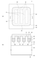
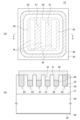
- FIG. 1(a) is a schematic plan view showing the configuration of a junction barrier Schottky diode 1 according to a first embodiment of the present invention.
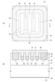
- FIG. 1(b) is a schematic cross-sectional view along line AA shown in FIG. 1(a).
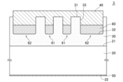
- FIGS. 2A to 2C are schematic cross-sectional views for explaining the positions of the inner walls of the central trench 61 and the peripheral trench 62 that are covered with the p-type semiconductor material 80.
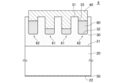
- FIG. FIG. 3 is a schematic cross-sectional view showing the configuration of a junction barrier Schottky diode 2 according to a second embodiment of the invention.
- FIG. 4 is a schematic cross-sectional view showing the structure of a junction barrier Schottky diode 3 according to a third embodiment of the invention.
- FIG. 5 is a schematic cross-sectional view showing the structure of a junction barrier Schottky diode 4 according to a fourth embodiment of the invention.
- FIG. 6 is a schematic cross-sectional view showing the structure of a junction barrier Schottky diode 5 according to a fifth embodiment of the invention.
- FIG. 7 is a schematic cross-sectional view showing the structure of a junction barrier Schottky diode 6 according to a sixth embodiment of the invention.
- FIG. 8(a) is a schematic plan view showing the configuration of a junction barrier Schottky diode 7 according to a seventh embodiment of the present invention.
- FIG. 8(b) is a schematic cross-sectional view along line AA shown in FIG. 8(a).
- FIG. 8(a) is a schematic cross-sectional view along line AA shown in FIG. 8(a).
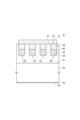
- FIG. 9 is a schematic cross-sectional view showing the structure of a junction barrier Schottky diode 8 according to an eighth embodiment of the invention.
- FIG. 10 is a schematic cross-sectional view showing the structure of a junction barrier Schottky diode 9 according to the ninth embodiment of the invention.
- FIG. 11 is a schematic cross-sectional view showing the structure of a junction barrier Schottky diode 10 according to a tenth embodiment of the invention.
- FIG. 12 is a schematic cross-sectional view showing the structure of a junction barrier Schottky diode 11 according to the eleventh embodiment of the invention.
- FIG. 13(a) is a schematic plan view showing the configuration of a junction barrier Schottky diode 12 according to the twelfth embodiment of the present invention.
- FIG. 13(b) is a schematic cross-sectional view along line AA shown in FIG. 13(a).
- FIG. 14(a) is a schematic plan view showing the configuration of a junction barrier Schottky diode 13 according to the thirteenth embodiment of the present invention.
- FIG. 14(b) is a schematic cross-sectional view taken along line AA shown in FIG. 14(a).
- FIG. 15(a) is a schematic plan view showing the configuration of a junction barrier Schottky diode 14 according to the fourteenth embodiment of the present invention.
- FIG. 15(b) is a schematic cross-sectional view along line AA shown in FIG. 15(a).
- FIG. 16 is a schematic cross-sectional view showing the structure of a junction barrier Schottky diode 15 according to a fifteenth embodiment of the invention.
- FIG. 17 is a graph showing simulation results of the example.
- FIG. 1(a) is a schematic plan view showing the configuration of a junction barrier Schottky diode 1 according to a first embodiment of the present invention.
- FIG. 1(b) is a schematic cross-sectional view along line AA shown in FIG. 1(a).
- the junction barrier Schottky diode 1 includes a semiconductor substrate 20 and a drift layer 30 both made of gallium oxide ( ⁇ -Ga 2 O 3 ). Silicon (Si) or tin (Sn) is introduced into the semiconductor substrate 20 and the drift layer 30 as an n-type dopant.
- the dopant concentration is higher in the semiconductor substrate 20 than in the drift layer 30, so that the semiconductor substrate 20 functions as an n + layer and the drift layer 30 functions as an n ⁇ layer.
- the semiconductor substrate 20 is obtained by cutting a bulk crystal formed using a melt growth method or the like, and its thickness is about 250 ⁇ m.
- the planar size of the semiconductor substrate 20 is not particularly limited, but is generally selected according to the amount of current flowing through the element. It may be about 2.4 mm.
- the semiconductor substrate 20 has an upper surface 21 positioned on the upper surface side during mounting, and a back surface 22 positioned on the lower surface side during mounting on the opposite side of the upper surface 21 .
- a drift layer 30 is formed on the entire upper surface 21 .
- the drift layer 30 is a thin film obtained by epitaxially growing gallium oxide on the upper surface 21 of the semiconductor substrate 20 using reactive sputtering, PLD, MBE, MOCVD, HVPE, or the like. Although the thickness of the drift layer 30 is not particularly limited, it is generally selected according to the reverse withstand voltage of the device.
- An anode electrode 40 is formed on the upper surface 31 of the drift layer 30 to make Schottky contact with the drift layer 30 .
- the anode electrode 40 is made of metal such as platinum (Pt), palladium (Pd), gold (Au), nickel (Ni), molybdenum (Mo), and copper (Cu).
- the anode electrode 40 may be a multi-layer structure in which different metal films are laminated, such as Pt/Au, Pt/Al, Pd/Au, Pd/Al, Pt/Ti/Au or Pd/Ti/Au.
- the back surface 22 of the semiconductor substrate 20 is provided with a cathode electrode 50 that makes ohmic contact with the semiconductor substrate 20 .
- the cathode electrode 50 is made of metal such as titanium (Ti).
- the cathode electrode 50 may have a multi-layer structure in which different metal films are laminated, such as Ti/Au or Ti/Al.
- the drift layer 30 is provided with a central trench 61 and a peripheral trench 62 . Both the central trench 61 and the peripheral trench 62 are provided at positions overlapping with the anode electrode 40 in plan view, and are filled with the same metal material as the anode electrode 40 and the p-type semiconductor material 80 .
- a p-type semiconductor material 80 is in contact with the anode electrode 40 .
- Si, GaAs, GaN, SiC, Ge, ZnSe, CdS, InP, SiGe, AlN, BN, AlGaN, NiO, Cu2O , Ir2O3 , and Ag2O are used as the p-type semiconductor material 80.
- Center trench 61 is sandwiched between mesa regions M that are part of drift layer 30 .
- the outer trench 62 surrounds the mesa region M and the central trench 61 in a ring shape.
- the central trench 61 and the peripheral trench 62 do not need to be completely separated, and may be connected to each other as shown in FIG. 1(a).
- the central trench 61 and the peripheral trench 62 may have the same depth or may have different depths.
- the mesa region M is a part of the drift layer 30 defined by the central trench 61 and the peripheral trench 62 and becomes a depletion layer when a reverse voltage is applied between the anode electrode 40 and the cathode electrode 50 .
- the channel region of the drift layer 30 is pinched off, thereby greatly suppressing leakage current when a reverse voltage is applied.
- a p-type semiconductor material 80 is embedded in the bottom of the central trench 61 and the peripheral trench 62
- an anode electrode 40 is embedded in the upper part of the central trench 61 and the peripheral trench 62 . Therefore, among the inner walls of the central trench 61 and the peripheral trench 62, lower portions of the bottom surface 32 and the side surfaces 33 are in contact with the p-type semiconductor material 80, and among the inner walls of the central trench 61 and the peripheral trench 62, upper portions of the side surfaces 33 are in contact with the p-type semiconductor material 80. It is in contact with the anode electrode 40 .
- the drift layer 30 and the anode electrode 40 are in Schottky contact not only at the upper surface 31 of the drift layer 30 but also at the upper portions of the side surfaces 33 of the central trench 61 and the peripheral trench 62 . are all buried with the p-type semiconductor material 80, the on-resistance is reduced.
- the dopant concentration of the drift layer 30 can be suppressed to about 3 ⁇ 10 16 cm ⁇ 3 , a decrease in reverse withstand voltage is also prevented.
- FIG. 2A when the bottom surfaces 32 of the central trench 61 and the peripheral trench 62 are horizontal, and the portions located between the horizontal bottom surfaces 32 and the vertical side surfaces 33 are the curved surfaces 34. , the bottom surface 32 and the curved surface 34 must be covered with a p-type semiconductor material 80 .
- FIG. 2B when the bottom surfaces 32 of the central trench 61 and the peripheral trench 62 are curved as a whole, the entire curved bottom surfaces 32 need to be covered with the p-type semiconductor material 80.
- FIG. 2B when the bottom surfaces 32 of the central trench 61 and the peripheral trench 62 are curved as a whole, the entire curved bottom surfaces 32 need to be covered with the p-type semiconductor material 80.
- the anode electrode 40 is in Schottky contact with the upper portion of the side surface 33 of the central trench 61 and the peripheral trench 62, so that the central trench 61 and the peripheral trench 62 are all p
- the on-resistance can be reduced as compared with the case of embedding with the semiconductor material 80 of the mold.
- FIG. 3 is a schematic cross-sectional view showing the configuration of a junction barrier Schottky diode 2 according to a second embodiment of the invention.
- the junction barrier Schottky diode 2 includes a film of a p-type semiconductor material 80 that covers the lower portions of the bottom surface 32 and side surfaces 33 of the inner walls of the central trench 61 and the peripheral trench 62. It is different from the junction barrier Schottky diode 1 according to the first embodiment in that the thickness is small, so that the anode electrode 40 is also buried in the bottoms of the central trench 61 and the peripheral trench 62 . Since other basic configurations are the same as those of the junction barrier Schottky diode 1 according to the first embodiment, the same elements are denoted by the same reference numerals, and overlapping descriptions are omitted. As illustrated in this embodiment, the p-type semiconductor material 80 need not fill the entire bottom of the central trench 61 and the outer peripheral trench 62, and may cover only the surfaces thereof.
- FIG. 4 is a schematic cross-sectional view showing the structure of a junction barrier Schottky diode 3 according to a third embodiment of the invention.
- the width of the peripheral trench 62 is wider than the width of the central trench 61. It differs from the key diode 1. Since other basic configurations are the same as those of the junction barrier Schottky diode 1 according to the first embodiment, the same elements are denoted by the same reference numerals, and overlapping descriptions are omitted. By increasing the width of the outer trench 62 in this way, it is possible to alleviate the electric field concentrated near the bottom of the outer trench 62 when a reverse voltage is applied.
- FIG. 5 is a schematic cross-sectional view showing the structure of a junction barrier Schottky diode 4 according to a fourth embodiment of the invention.
- the junction barrier Schottky diode 4 according to the fourth embodiment differs from the junction barrier Schottky diode 4 according to the first embodiment in that the drift layer 30 located outside the outer peripheral trench 62 is removed.
- Diode 1 is different. Since other basic configurations are the same as those of the junction barrier Schottky diode 1 according to the first embodiment, the same elements are denoted by the same reference numerals, and overlapping descriptions are omitted. Since almost no on-current flows in the portion of the drift layer 30 located outside the outer peripheral trench 62, the drift layer 30 located in this portion may be removed as exemplified in this embodiment.
- FIG. 6 is a schematic cross-sectional view showing the structure of a junction barrier Schottky diode 5 according to a fifth embodiment of the invention.
- an insulating film 71 is provided between the upper surface 31 of the drift layer 30 located outside the peripheral trench 62 and the anode electrode 40. In this point, it differs from the junction barrier Schottky diode 1 according to the first embodiment. Since other basic configurations are the same as those of the junction barrier Schottky diode 1 according to the first embodiment, the same elements are denoted by the same reference numerals, and overlapping descriptions are omitted.
- As a material for the insulating film 71 it is desirable to use a material having a high withstand voltage such as SiO 2 or Al 2 O 3 . According to this, the pressure resistance effect is enhanced. According to the present embodiment, a so-called field plate structure is obtained by the insulating film 71, so that the electric field applied to the bottom of the outer peripheral trench 62 can be further relaxed.
- FIG. 7 is a schematic cross-sectional view showing the structure of a junction barrier Schottky diode 6 according to a sixth embodiment of the invention.
- the anode electrode 41 covering the upper surface of the drift layer 30 and the anode electrode 42 embedded in the central trench 61 and the peripheral trench 62 are made of different metals. It differs from the junction barrier Schottky diode 1 according to the first embodiment in that it is made of material. Since other basic configurations are the same as those of the junction barrier Schottky diode 1 according to the first embodiment, the same elements are denoted by the same reference numerals, and overlapping descriptions are omitted.
- Such a structure can be obtained, for example, by forming the anode electrode 42 by electrolytic plating and forming the anode electrode 41 by vapor deposition. According to such a manufacturing method, voids are less likely to occur in the anode electrode 42 embedded in the central trench 61 and the peripheral trench 62 .
- FIG. 8(a) is a schematic plan view showing the configuration of a junction barrier Schottky diode 7 according to a seventh embodiment of the present invention.
- FIG. 8(b) is a schematic cross-sectional view along line AA shown in FIG. 8(a).
- the junction barrier Schottky diode 7 according to the seventh embodiment has a junction barrier shot similar to that of the first embodiment in that the entire outer trench 62 is filled with a p-type semiconductor material 80 . It differs from the key diode 1. Since other basic configurations are the same as those of the junction barrier Schottky diode 1 according to the first embodiment, the same elements are denoted by the same reference numerals, and overlapping descriptions are omitted.
- FIG. 8A the surface of the mesa region M that is in Schottky contact with the drift layer 30 is indicated by a broken line, and the surface of the mesa region M that is covered with the p-type semiconductor material 80 is indicated by a solid line. ing. According to this, it becomes possible to further increase the reverse breakdown voltage.
- FIG. 9 is a schematic cross-sectional view showing the structure of a junction barrier Schottky diode 8 according to an eighth embodiment of the invention.
- the height position of the p-type semiconductor material 80 embedded in the outer trench 62 is the junction barrier Schottky diode according to the seventh embodiment. 7, thereby making a part of the side surface 33 of the outer trench 62 in Schottky contact with the anode electrode 40, which is different from the junction barrier Schottky diode 7 according to the seventh embodiment. Since other basic configurations are the same as those of the junction barrier Schottky diode 7 according to the seventh embodiment, the same elements are denoted by the same reference numerals, and overlapping descriptions are omitted. According to this embodiment, it is possible to increase the reverse breakdown voltage and lower the on-resistance than the junction barrier Schottky diode 7 according to the seventh embodiment.
- FIG. 10 is a schematic cross-sectional view showing the structure of a junction barrier Schottky diode 9 according to the ninth embodiment of the invention.
- the p-type semiconductor material 80 is replaced with the anode electrode 40 at the portion of the side surface 33 of the outer trench 62 that is in contact with the inner side surface 33a.
- the outer side surface 33 b is entirely covered with a p-type semiconductor material 80 . Since other basic configurations are the same as those of the junction barrier Schottky diode 7 according to the seventh embodiment, the same elements are denoted by the same reference numerals, and overlapping descriptions are omitted. Also in this embodiment, it is possible to increase the reverse breakdown voltage and lower the on-resistance than the junction barrier Schottky diode 7 according to the seventh embodiment.
- FIG. 11 is a schematic cross-sectional view showing the structure of a junction barrier Schottky diode 10 according to a tenth embodiment of the invention.
- the anode electrode 41 covering the upper surface of the drift layer 30 and the anode electrode 42 embedded in the central trench 61 are made of different metal materials. is different from the junction barrier Schottky diode 7 according to the seventh embodiment. Since other basic configurations are the same as those of the junction barrier Schottky diode 7 according to the seventh embodiment, the same elements are denoted by the same reference numerals, and overlapping descriptions are omitted.
- Such a structure can be obtained, for example, by forming the anode electrode 42 by electrolytic plating and forming the anode electrode 41 by vapor deposition. According to such a manufacturing method, voids are less likely to occur in the anode electrode 42 embedded in the central trench 61 and the peripheral trench 62 .
- FIG. 12 is a schematic cross-sectional view showing the structure of a junction barrier Schottky diode 11 according to the eleventh embodiment of the invention.
- the inner wall of the outer trench 62 is covered with an insulating film 70 , and the outer trench 62 is connected to the anode electrode 40 via the insulating film 70 .
- the junction barrier Schottky diode 7 according to the seventh embodiment it is different from the junction barrier Schottky diode 7 according to the seventh embodiment in that it is embedded. Since other basic configurations are the same as those of the junction barrier Schottky diode 7 according to the seventh embodiment, the same elements are denoted by the same reference numerals, and overlapping descriptions are omitted. Also in this embodiment, as in the seventh embodiment, it is possible to further increase the reverse breakdown voltage.
- the material of the insulating film 70 it is desirable to use an insulating material having a high dielectric constant such as HfO 2 or Al 2 O 3 . According to this, the pressure resistance effect is enhanced.
- FIG. 13(a) is a schematic plan view showing the configuration of a junction barrier Schottky diode 12 according to the twelfth embodiment of the present invention.
- FIG. 13(b) is a schematic cross-sectional view along line AA shown in FIG. 13(a).
- another peripheral trench 63 surrounding the peripheral trench 62 is provided in the drift layer 30, and the entire peripheral trench 63 is a p-type semiconductor. It differs from the junction barrier Schottky diode 1 according to the first embodiment in that it is filled with a material 80 .
- the outer trench 63 is provided independently of the outer trench 62 . Since other basic configurations are the same as those of the junction barrier Schottky diode 1 according to the first embodiment, the same elements are denoted by the same reference numerals, and overlapping descriptions are omitted. In FIG.
- the surface of the mesa region M that is in Schottky contact with the drift layer 30 is indicated by a broken line
- the surface of the mesa region M that is covered with the p-type semiconductor material 80 is indicated by a solid line.
- FIG. 14(a) is a schematic plan view showing the configuration of a junction barrier Schottky diode 13 according to the thirteenth embodiment of the present invention. Also, FIG. 14(b) is a schematic cross-sectional view taken along line AA shown in FIG. 14(a).
- the junction barrier Schottky diode 13 according to the thirteenth embodiment differs from the twelfth embodiment in that the width of the peripheral trench 63 is wider than the widths of the central trench 61 and the peripheral trench 62 . is different from the junction barrier Schottky diode 12 by Since other basic configurations are the same as those of the junction barrier Schottky diode 12 according to the twelfth embodiment, the same elements are denoted by the same reference numerals, and overlapping descriptions are omitted. By increasing the width of the outer trench 63 in this way, it is possible to relax the electric field concentrated near the bottom of the outer trench 63 when a reverse voltage is applied.
- FIG. 15(a) is a schematic plan view showing the configuration of a junction barrier Schottky diode 14 according to the fourteenth embodiment of the present invention.
- FIG. 15(b) is a schematic cross-sectional view along line AA shown in FIG. 15(a).
- the inner wall of the outer trench 63 is covered with an insulating film 70 made of HfO 2 or the like. It differs from the junction barrier Schottky diode 12 according to the twelfth embodiment in that it is embedded with an electrode 40 . Since other basic configurations are the same as those of the junction barrier Schottky diode 12 according to the twelfth embodiment, the same elements are denoted by the same reference numerals, and overlapping descriptions are omitted. Also in this embodiment, as in the twelfth embodiment, it is possible to further increase the reverse breakdown voltage.
- FIG. 16 is a schematic cross-sectional view showing the structure of a junction barrier Schottky diode 15 according to a fifteenth embodiment of the invention.
- the anode electrode 41 in Schottky contact with the drift layer 30 is made of a Cu single layer film or a Cu/Al laminated film. It is different from the junction barrier Schottky diode 2 according to the second embodiment in that the anode electrode 42 that is in ohmic contact with the semiconductor material 80 of the mold is made of Ni or the like. Since other basic configurations are the same as those of the junction barrier Schottky diode 2 according to the second embodiment, the same elements are denoted by the same reference numerals, and overlapping descriptions are omitted.
- the p-type semiconductor material 80 and the anode electrode 42 can be brought into ohmic contact. becomes possible, and the contact resistance is reduced.
- the p-type semiconductor material 80 is NiO
- Ni is used as the anode electrode 42
- both can be brought into ohmic contact.
- the p-type semiconductor material 80 is made of a material having a wider bandgap than NiO, it is preferable to use a metal such as Pt having a larger work function than Ni as the anode electrode 42 .
- Example 1> Assuming a simulation model of an embodiment having the same structure as the junction barrier Schottky diode 1 shown in FIG. .
- the dopant concentration of the semiconductor substrate 20 was set to 1 ⁇ 10 18 cm ⁇ 3 and the dopant concentration of the drift layer 30 was set to 3 ⁇ 10 16 cm ⁇ 3 .
- the thickness of the drift layer 30 was set to 7 ⁇ m.
- the depths of the central trench 61 and the peripheral trench 62 were both set to 3 ⁇ m.
- the widths of the central trench 61 and the peripheral trench 62 and the width of the upper surface 31 of the drift layer 30 (the width of the mesa region M) in the cross section shown in FIG. 1B are all set to 1.5 ⁇ m.
- the curvature radius of the curved surface 34 positioned between the flat bottom surface 32 and the side surface 33 of the central trench 61 and the outer peripheral trench 62 was set to 0.2 ⁇ m.
- NiO was used as the p-type semiconductor material 80 .
- the material of the anode electrode 40 was Ni, and the material of the cathode electrode 50 was a laminated film of Ti and Au.
- a simulation was performed using the depth T of the anode electrode 40 in contact with the side surfaces 33 of the central trench 61 and the peripheral trench 62 as a variable.
- junction barrier Schottky diode 20 semiconductor substrate 21 top surface 22 of semiconductor substrate back surface 30 drift layer 31 top surface of drift layer 32 bottom surface of trench 33 side surface 33a of trench inner side surface 33b inner side surface 33b of trench outer side surface 34 of trench curved surface 35 trench corners 40 to 42 anode electrode 50 cathode electrode 61 central trenches 62, 63 outer trenches 70, 71 insulating film 80 semiconductor material M mesa region
Landscapes
- Electrodes Of Semiconductors (AREA)
Abstract
【課題】酸化ガリウムを用いたジャンクションバリアショットキーダイオードにおいて、十分な逆方向耐圧を確保しつつオン抵抗を低減する。 【解決手段】ジャンクションバリアショットキーダイオード1は、酸化ガリウムからなる半導体基板20と、半導体基板20上に設けられた酸化ガリウムからなるドリフト層30と、ドリフト層30とショットキー接触するアノード電極40と、半導体基板20とオーミック接触するカソード電極50とを備える。ドリフト層30は、アノード電極40及びドリフト層30とは導電型が逆の半導体材料80が埋め込まれた中心トレンチ61を有する。中心トレンチ61の底面32は、アノード電極40と接することなく半導体材料80と接し、中心トレンチ61の側面33の少なくとも一部はアノード電極40とショットキー接触する。これにより、ドリフト層の不純物濃度を高めることなく、オン抵抗を低減することができる。
Description
本発明はジャンクションバリアショットキーダイオードに関し、特に、酸化ガリウムを用いたジャンクションバリアショットキーダイオードに関する。
ショットキーバリアダイオードは、金属と半導体の接合によって生じるショットキー障壁を利用した整流素子であり、PN接合を有する通常のダイオードに比べて順方向電圧が低く、且つ、スイッチング速度が速いという特徴を有している。このため、ショットキーバリアダイオードはパワーデバイス用のスイッチング素子として利用されることがある。
ショットキーバリアダイオードをパワーデバイス用のスイッチング素子として用いる場合、十分な逆方向耐圧を確保する必要があることから、シリコン(Si)の代わりに、よりバンドギャップの大きい炭化シリコン(SiC)、窒化ガリウム(GaN)、酸化ガリウム(Ga2O3)などが用いられることがある。中でも、酸化ガリウムは、バンドギャップが4.8~4.9eVと非常に大きく、絶縁破壊電界も約8MV/cmと大きいことから、酸化ガリウムを用いたショットキーバリアダイオードは、パワーデバイス用のスイッチング素子として非常に有望である。酸化ガリウムを用いたショットキーバリアダイオードの例は、特許文献1に記載されている。
特許文献1には、酸化ガリウム層に設けられた複数のトレンチをp型の半導体材料で埋め込んだ構造を有するジャンクションバリアショットキーダイオードが開示されている。このように、酸化ガリウム層に複数のトレンチを設けるとともに、複数のトレンチをp型の半導体材料で埋め込めば、逆方向電圧が印加されるとトレンチ間に位置するメサ領域が空乏層となるため、ドリフト層のチャネル領域がピンチオフされる。これにより、逆方向電圧が印加された場合のリーク電流を大幅に抑制することができる。
しかしながら、特許文献1に記載されたジャンクションバリアショットキーダイオードは、アノード電極とドリフト層がショットキー接触する面積が小さいことから、オン抵抗が高いという問題があった。オン抵抗を下げるためには、ドリフト層の不純物濃度を高めれば良いが、この場合には逆方向耐圧が低下してしまう。
したがって、本発明は、酸化ガリウムを用いたジャンクションバリアショットキーダイオードにおいて、十分な逆方向耐圧を確保しつつ、オン抵抗を低減することを目的とする。
本発明によるジャンクションバリアショットキーダイオードは、酸化ガリウムからなる半導体基板と、半導体基板上に設けられた酸化ガリウムからなるドリフト層と、ドリフト層とショットキー接触するアノード電極と、半導体基板とオーミック接触するカソード電極とを備え、ドリフト層は、アノード電極及びドリフト層とは導電型が逆の半導体材料が埋め込まれた中心トレンチを有し、中心トレンチの底面は、アノード電極と接することなく半導体材料と接し、中心トレンチの側面の少なくとも一部はアノード電極とショットキー接触することを特徴とする。
本発明によれば、中心トレンチに埋め込まれたアノード電極が中心トレンチの側面とショットキー接触することから、ドリフト層の不純物濃度を高めることなく、オン抵抗を低減することが可能となる。
本発明において、アノード電極は、ドリフト層の上面とショットキー接触する第1のアノード電極と、中心トレンチの側面とショットキー接触し、第1のアノード電極とは異なる金属材料からなる第2のアノード電極とを含んでいても構わない。これよれば、ボイドのないアノード電極を作製しやすくなる。
本発明において、ドリフト層は、中心トレンチを囲む外周トレンチをさらに有し、外周トレンチの底面及び外周側面は、アノード電極と接することなく半導体材料と接していても構わない。これによれば、逆方向電圧が印加された場合に外周トレンチの外周底部に生じる電界が緩和される。この場合、外周トレンチの内周側面の少なくとも一部は、アノード電極とショットキー接触しても構わない。これによれば、ショットキー接触する面積が拡大することから、オン抵抗をより低減することが可能となる。
本発明において、ドリフト層は、アノード電極が埋め込まれ、中心トレンチを囲む外周トレンチをさらに有し、外周トレンチの内壁は、アノード電極と接することなく絶縁膜で覆われていても構わない。これによれば、逆方向電圧が印加された場合に外周トレンチの外周底部に生じる電界が緩和される。
このように、本発明によれば、中心トレンチの側面がアノード電極とショットキー接触することから、酸化ガリウムを用いたジャンクションバリアショットキーダイオードのオン抵抗を低減することが可能となる。
以下、添付図面を参照しながら、本発明の好ましい実施形態について詳細に説明する。
<第1の実施形態>
図1(a)は、本発明の第1の実施形態によるジャンクションバリアショットキーダイオード1の構成を示す模式的な平面図である。また、図1(b)は、図1(a)に示すA-A線に沿った略断面図である。
図1(a)は、本発明の第1の実施形態によるジャンクションバリアショットキーダイオード1の構成を示す模式的な平面図である。また、図1(b)は、図1(a)に示すA-A線に沿った略断面図である。
図1に示すように、第1の実施形態によるジャンクションバリアショットキーダイオード1は、いずれも酸化ガリウム(β-Ga2O3)からなる半導体基板20及びドリフト層30を備える。半導体基板20及びドリフト層30には、n型ドーパントとしてシリコン(Si)又はスズ(Sn)が導入されている。ドーパントの濃度は、ドリフト層30よりも半導体基板20の方が高く、これにより半導体基板20はn+層、ドリフト層30はn-層として機能する。
半導体基板20は、融液成長法などを用いて形成されたバルク結晶を切断加工したものであり、その厚みは250μm程度である。半導体基板20の平面サイズについては特に限定されないが、一般的に素子に流す電流量に応じて選択することになり、順方向の最大電流量が20A程度であれば、平面視で2.4mm×2.4mm程度とすればよい。
半導体基板20は、実装時において上面側に位置する上面21と、上面21の反対側であって、実装時において下面側に位置する裏面22を有する。上面21の全面にはドリフト層30が形成されている。ドリフト層30は、半導体基板20の上面21に反応性スパッタリング、PLD法、MBE法、MOCVD法、HVPE法などを用いて酸化ガリウムをエピタキシャル成長させた薄膜である。ドリフト層30の膜厚については特に限定されないが、一般的に素子の逆方向耐電圧に応じて選択することになり、600V程度の耐圧を確保するためには、例えば7μm程度とすればよい。
ドリフト層30の上面31には、ドリフト層30とショットキー接触するアノード電極40が形成されている。アノード電極40は、例えば白金(Pt)、パラジウム(Pd)、金(Au)、ニッケル(Ni)、モリブデン(Mo)、銅(Cu)等の金属からなる。アノード電極40は、異なる金属膜を積層した多層構造、例えば、Pt/Au、Pt/Al、Pd/Au、Pd/Al、Pt/Ti/AuまたはPd/Ti/Auであっても構わない。一方、半導体基板20の裏面22には、半導体基板20とオーミック接触するカソード電極50が設けられる。カソード電極50は、例えばチタン(Ti)等の金属からなる。カソード電極50は、異なる金属膜を積層した多層構造、例えば、Ti/AuまたはTi/Alであっても構わない。
本実施形態においては、ドリフト層30に中心トレンチ61及び外周トレンチ62が設けられている。中心トレンチ61及び外周トレンチ62は、いずれも平面視でアノード電極40と重なる位置に設けられており、その内部はアノード電極40と同じ金属材料及びp型の半導体材料80で埋め込まれている。p型の半導体材料80はアノード電極40と接触している。p型の半導体材料80としては、Si、GaAs、GaN、SiC、Ge、ZnSe、CdS、InP、SiGe、AlN、BN、AlGaN、NiO、Cu2O、Ir2O3、Ag2Oを用いることができ、中でもNiOなどのp型酸化物は酸化の問題がないために好ましい。中心トレンチ61は、ドリフト層30の一部であるメサ領域Mに挟まれている。外周トレンチ62は、メサ領域M及び中心トレンチ61をリング状に囲んでいる。中心トレンチ61と外周トレンチ62が完全に分離されている必要はなく、図1(a)に示すように、中心トレンチ61と外周トレンチ62が繋がっていても構わない。中心トレンチ61と外周トレンチ62の深さは同じであっても構わないし、異なっていても構わない。メサ領域Mは、中心トレンチ61及び外周トレンチ62によって区画されるドリフト層30の一部であり、アノード電極40とカソード電極50との間に逆方向電圧が印加されると空乏層となる。これにより、ドリフト層30のチャネル領域がピンチオフされることから、逆方向電圧が印加された場合のリーク電流が大幅に抑制される。
中心トレンチ61及び外周トレンチ62の底部にはp型の半導体材料80が埋め込まれ、中心トレンチ61及び外周トレンチ62の上部にはアノード電極40が埋め込まれている。このため、中心トレンチ61及び外周トレンチ62の内壁のうち、底面32及び側面33の下部についてはp型の半導体材料80と接し、中心トレンチ61及び外周トレンチ62の内壁のうち、側面33の上部はアノード電極40と接する。これにより、ドリフト層30とアノード電極40は、ドリフト層30の上面31だけでなく、中心トレンチ61及び外周トレンチ62の側面33の上部においてもショットキー接触することから、中心トレンチ61及び外周トレンチ62を全てp型の半導体材料80で埋め込む場合と比べてオン抵抗が低減する。また、ドリフト層30のドーパント濃度については、3×1016cm-3程度に抑えることができるため、逆方向耐圧の低下も防止される。
ここで、図2(a)に示すように、中心トレンチ61及び外周トレンチ62の底面32が水平であり、水平な底面32と垂直な側面33の間に位置する部分が湾曲面34である場合、底面32及び湾曲面34についてはp型の半導体材料80で覆われている必要がある。また、図2(b)に示すように、中心トレンチ61及び外周トレンチ62の底面32が全体的に湾曲している場合、湾曲した底面32全体がp型の半導体材料80で覆われている必要がある。さらに、図2(c)に示すように、中心トレンチ61及び外周トレンチ62の底面32が水平であり、水平な底面32と垂直な側面33の間に直角な角部35が存在する場合、底面32及び角部35についてはp型の半導体材料80で覆われている必要がある。
このように、本実施形態によるジャンクションバリアショットキーダイオード1は、中心トレンチ61及び外周トレンチ62の側面33の上部においてアノード電極40がショットキー接触することから、中心トレンチ61及び外周トレンチ62を全てp型の半導体材料80で埋め込む場合と比べ、オン抵抗を低減することが可能となる。
<第2の実施形態>
図3は、本発明の第2の実施形態によるジャンクションバリアショットキーダイオード2の構成を示す略断面図である。
図3は、本発明の第2の実施形態によるジャンクションバリアショットキーダイオード2の構成を示す略断面図である。
図3に示すように、第2の実施形態によるジャンクションバリアショットキーダイオード2は、中心トレンチ61及び外周トレンチ62の内壁のうち、底面32及び側面33の下部を覆うp型の半導体材料80の膜厚が薄く、これにより、中心トレンチ61及び外周トレンチ62の底部にもアノード電極40が埋め込まれている点において、第1の実施形態によるジャンクションバリアショットキーダイオード1と相違している。その他の基本的な構成は第1の実施形態によるジャンクションバリアショットキーダイオード1と同一であることから、同一の要素には同一の符号を付し、重複する説明は省略する。本実施形態が例示するように、p型の半導体材料80は、中心トレンチ61及び外周トレンチ62の底部全体を埋め込む必要はなく、その表面のみを覆うものであっても構わない。
<第3の実施形態>
図4は、本発明の第3の実施形態によるジャンクションバリアショットキーダイオード3の構成を示す略断面図である。
図4は、本発明の第3の実施形態によるジャンクションバリアショットキーダイオード3の構成を示す略断面図である。
図4に示すように、第3の実施形態によるジャンクションバリアショットキーダイオード3は、外周トレンチ62の幅が中心トレンチ61の幅よりも拡大されている点において、第1の実施形態によるジャンクションバリアショットキーダイオード1と相違している。その他の基本的な構成は第1の実施形態によるジャンクションバリアショットキーダイオード1と同一であることから、同一の要素には同一の符号を付し、重複する説明は省略する。このように、外周トレンチ62の幅を拡大すれば、逆方向電圧が印加された場合に外周トレンチ62の底部近傍に集中する電界を緩和することが可能となる。
<第4の実施形態>
図5は、本発明の第4の実施形態によるジャンクションバリアショットキーダイオード4の構成を示す略断面図である。
図5は、本発明の第4の実施形態によるジャンクションバリアショットキーダイオード4の構成を示す略断面図である。
図5に示すように、第4の実施形態によるジャンクションバリアショットキーダイオード4は、外周トレンチ62の外側に位置するドリフト層30が削除されている点において、第1の実施形態によるジャンクションバリアショットキーダイオード1と相違している。その他の基本的な構成は第1の実施形態によるジャンクションバリアショットキーダイオード1と同一であることから、同一の要素には同一の符号を付し、重複する説明は省略する。ドリフト層30のうち、外周トレンチ62の外側に位置する部分にはオン電流がほとんど流れないため、本実施形態が例示するように、この部分に位置するドリフト層30を除去しても構わない。
<第5の実施形態>
図6は、本発明の第5の実施形態によるジャンクションバリアショットキーダイオード5の構成を示す略断面図である。
図6は、本発明の第5の実施形態によるジャンクションバリアショットキーダイオード5の構成を示す略断面図である。
図6に示すように、第5の実施形態によるジャンクションバリアショットキーダイオード6は、外周トレンチ62の外側に位置するドリフト層30の上面31とアノード電極40の間に絶縁膜71が設けられている点において、第1の実施形態によるジャンクションバリアショットキーダイオード1と相違している。その他の基本的な構成は第1の実施形態によるジャンクションバリアショットキーダイオード1と同一であることから、同一の要素には同一の符号を付し、重複する説明は省略する。絶縁膜71の材料としては、SiO2やAl2O3など絶縁耐圧の高い材料を用いることが望ましい。これによれば、耐圧効果が高められる。本実施形態によれば、絶縁膜71によっていわゆるフィールドプレート構造が得られることから、外周トレンチ62の底部に印加される電界をより緩和することが可能となる。
<第6の実施形態>
図7は、本発明の第6の実施形態によるジャンクションバリアショットキーダイオード6の構成を示す略断面図である。
図7は、本発明の第6の実施形態によるジャンクションバリアショットキーダイオード6の構成を示す略断面図である。
図7に示すように、第6の実施形態によるジャンクションバリアショットキーダイオード6は、ドリフト層30の上面を覆うアノード電極41と中心トレンチ61及び外周トレンチ62に埋め込まれたアノード電極42が互いに異なる金属材料からなる点において、第1の実施形態によるジャンクションバリアショットキーダイオード1と相違している。その他の基本的な構成は第1の実施形態によるジャンクションバリアショットキーダイオード1と同一であることから、同一の要素には同一の符号を付し、重複する説明は省略する。このような構造は、例えば、アノード電極42を電解メッキによって形成し、アノード電極41を蒸着によって形成することによって得られる。このような製法によれば、中心トレンチ61及び外周トレンチ62に埋め込まれたアノード電極42にボイドが生じにくくなる。
<第7の実施形態>
図8(a)は、本発明の第7の実施形態によるジャンクションバリアショットキーダイオード7の構成を示す模式的な平面図である。また、図8(b)は、図8(a)に示すA-A線に沿った略断面図である。
図8(a)は、本発明の第7の実施形態によるジャンクションバリアショットキーダイオード7の構成を示す模式的な平面図である。また、図8(b)は、図8(a)に示すA-A線に沿った略断面図である。
図8に示すように、第7の実施形態によるジャンクションバリアショットキーダイオード7は、外周トレンチ62の全体がp型の半導体材料80で埋め込まれている点において、第1の実施形態によるジャンクションバリアショットキーダイオード1と相違している。その他の基本的な構成は第1の実施形態によるジャンクションバリアショットキーダイオード1と同一であることから、同一の要素には同一の符号を付し、重複する説明は省略する。図8(a)においては、メサ領域Mの表面のうちドリフト層30とショットキー接触する面を破線で示し、メサ領域Mの表面のうちp型の半導体材料80で覆われる面を実線で示している。これによれば、逆方向耐圧をより高めることが可能となる。
<第8の実施形態>
図9は、本発明の第8の実施形態によるジャンクションバリアショットキーダイオード8の構成を示す略断面図である。
図9は、本発明の第8の実施形態によるジャンクションバリアショットキーダイオード8の構成を示す略断面図である。
図9に示すように、第8の実施形態によるジャンクションバリアショットキーダイオード8は、外周トレンチ62に埋め込まれたp型の半導体材料80の高さ位置が第7の実施形態によるジャンクションバリアショットキーダイオード7よりも低く、これにより、外周トレンチ62の側面33の一部がアノード電極40とショットキー接触する点において、第7の実施形態によるジャンクションバリアショットキーダイオード7と相違している。その他の基本的な構成は第7の実施形態によるジャンクションバリアショットキーダイオード7と同一であることから、同一の要素には同一の符号を付し、重複する説明は省略する。本実施形態によれば、逆方向耐圧を高めつつ、第7の実施形態によるジャンクションバリアショットキーダイオード7よりもオン抵抗を下げることが可能となる。
<第9の実施形態>
図10は、本発明の第9の実施形態によるジャンクションバリアショットキーダイオード9の構成を示す略断面図である。
図10は、本発明の第9の実施形態によるジャンクションバリアショットキーダイオード9の構成を示す略断面図である。
図10に示すように、第9の実施形態によるジャンクションバリアショットキーダイオード9は、外周トレンチ62の側面33のうち、内側側面33aと接する部分がp型の半導体材料80からアノード電極40に置き換えられている点において、第7の実施形態によるジャンクションバリアショットキーダイオード7と相違している。外周トレンチ62の側面33のうち、外側側面33bについては全面がp型の半導体材料80で覆われている。その他の基本的な構成は第7の実施形態によるジャンクションバリアショットキーダイオード7と同一であることから、同一の要素には同一の符号を付し、重複する説明は省略する。本実施形態においても、逆方向耐圧を高めつつ、第7の実施形態によるジャンクションバリアショットキーダイオード7よりもオン抵抗を下げることが可能となる。
<第10の実施形態>
図11は、本発明の第10の実施形態によるジャンクションバリアショットキーダイオード10の構成を示す略断面図である。
図11は、本発明の第10の実施形態によるジャンクションバリアショットキーダイオード10の構成を示す略断面図である。
図11に示すように、第10の実施形態によるジャンクションバリアショットキーダイオード10は、ドリフト層30の上面を覆うアノード電極41と中心トレンチ61に埋め込まれたアノード電極42が互いに異なる金属材料からなる点において、第7の実施形態によるジャンクションバリアショットキーダイオード7と相違している。その他の基本的な構成は第7の実施形態によるジャンクションバリアショットキーダイオード7と同一であることから、同一の要素には同一の符号を付し、重複する説明は省略する。このような構造は、例えば、アノード電極42を電解メッキによって形成し、アノード電極41を蒸着によって形成することによって得られる。このような製法によれば、中心トレンチ61及び外周トレンチ62に埋め込まれたアノード電極42にボイドが生じにくくなる。
<第11の実施形態>
図12は、本発明の第11の実施形態によるジャンクションバリアショットキーダイオード11の構成を示す略断面図である。
図12は、本発明の第11の実施形態によるジャンクションバリアショットキーダイオード11の構成を示す略断面図である。
図12に示すように、第11の実施形態によるジャンクションバリアショットキーダイオード11は、外周トレンチ62の内壁が絶縁膜70で覆われており、絶縁膜70を介して外周トレンチ62がアノード電極40で埋め込まれている点において、第7の実施形態によるジャンクションバリアショットキーダイオード7と相違している。その他の基本的な構成は第7の実施形態によるジャンクションバリアショットキーダイオード7と同一であることから、同一の要素には同一の符号を付し、重複する説明は省略する。本実施形態においても、第7の実施形態と同様、逆方向耐圧をより高めることが可能となる。絶縁膜70の材料としては、HfO2やAl2O3など誘電率の高い絶縁材料を用いることが望ましい。これによれば、耐圧効果が高められる。
<第12の実施形態>
図13(a)は、本発明の第12の実施形態によるジャンクションバリアショットキーダイオード12の構成を示す模式的な平面図である。また、図13(b)は、図13(a)に示すA-A線に沿った略断面図である。
図13(a)は、本発明の第12の実施形態によるジャンクションバリアショットキーダイオード12の構成を示す模式的な平面図である。また、図13(b)は、図13(a)に示すA-A線に沿った略断面図である。
図13に示すように、第12の実施形態によるジャンクションバリアショットキーダイオード12は、外周トレンチ62を取り囲む別の外周トレンチ63がドリフト層30に設けられ、この外周トレンチ63の全体がp型の半導体材料80で埋め込まれている点において、第1の実施形態によるジャンクションバリアショットキーダイオード1と相違している。外周トレンチ63は、外周トレンチ62とは独立して設けられている。その他の基本的な構成は第1の実施形態によるジャンクションバリアショットキーダイオード1と同一であることから、同一の要素には同一の符号を付し、重複する説明は省略する。図13(a)においては、メサ領域Mの表面のうちドリフト層30とショットキー接触する面を破線で示し、メサ領域Mの表面のうちp型の半導体材料80で覆われる面を実線で示している。このように、ドリフト層30に別の外周トレンチ63を設けるとともに、その内部全体をp型の半導体材料80で埋め込めば、逆方向電圧が印加された場合に中心トレンチ61及び外周トレンチ62の底部近傍に集中する電界を緩和することが可能となる。
<第13の実施形態>
図14(a)は、本発明の第13の実施形態によるジャンクションバリアショットキーダイオード13の構成を示す模式的な平面図である。また、図14(b)は、図14(a)に示すA-A線に沿った略断面図である。
図14(a)は、本発明の第13の実施形態によるジャンクションバリアショットキーダイオード13の構成を示す模式的な平面図である。また、図14(b)は、図14(a)に示すA-A線に沿った略断面図である。
図14に示すように、第13の実施形態によるジャンクションバリアショットキーダイオード13は、外周トレンチ63の幅が中心トレンチ61及び外周トレンチ62の幅よりも拡大されている点において、第12の実施形態によるジャンクションバリアショットキーダイオード12と相違している。その他の基本的な構成は第12の実施形態によるジャンクションバリアショットキーダイオード12と同一であることから、同一の要素には同一の符号を付し、重複する説明は省略する。このように、外周トレンチ63の幅を拡大すれば、逆方向電圧が印加された場合に外周トレンチ63の底部近傍に集中する電界を緩和することが可能となる。
<第14の実施形態>
図15(a)は、本発明の第14の実施形態によるジャンクションバリアショットキーダイオード14の構成を示す模式的な平面図である。また、図15(b)は、図15(a)に示すA-A線に沿った略断面図である。
図15(a)は、本発明の第14の実施形態によるジャンクションバリアショットキーダイオード14の構成を示す模式的な平面図である。また、図15(b)は、図15(a)に示すA-A線に沿った略断面図である。
図15に示すように、第14の実施形態によるジャンクションバリアショットキーダイオード14は、外周トレンチ63の内壁がHfO2などからなる絶縁膜70で覆われ、絶縁膜70を介して外周トレンチ63がアノード電極40で埋め込まれている点において、第12の実施形態によるジャンクションバリアショットキーダイオード12と相違している。その他の基本的な構成は第12の実施形態によるジャンクションバリアショットキーダイオード12と同一であることから、同一の要素には同一の符号を付し、重複する説明は省略する。本実施形態においても、第12の実施形態と同様、逆方向耐圧をより高めることが可能となる。
<第15の実施形態>
図16は、本発明の第15の実施形態によるジャンクションバリアショットキーダイオード15の構成を示す略断面図である。
図16は、本発明の第15の実施形態によるジャンクションバリアショットキーダイオード15の構成を示す略断面図である。
図16に示すように、第15の実施形態によるジャンクションバリアショットキーダイオード15は、ドリフト層30とショットキー接触するアノード電極41がCuの単層膜やCu/Alの積層膜などからなり、p型の半導体材料80とオーミック接触するアノード電極42がNiなどからなる点において、第2の実施形態によるジャンクションバリアショットキーダイオード2と相違している。その他の基本的な構成は第2の実施形態によるジャンクションバリアショットキーダイオード2と同一であることから、同一の要素には同一の符号を付し、重複する説明は省略する。このように、p型の半導体材料80と接するアノード電極42の材料として、ドリフト層30と接するアノード電極41とは異なる材料を用いれば、p型の半導体材料80とアノード電極42をオーミック接触させることが可能となり、接触抵抗が低減する。一例として、p型の半導体材料80がNiOである場合、アノード電極42としてNiを用いれば、両者をオーミック接触させることができる。また、p型の半導体材料80がNiOよりもバンドギャップが広い材料からなる場合、アノード電極42としては、Niよりも仕事関数の大きいPtなどの金属を用いることが好ましい。
以上、本発明の好ましい実施形態について説明したが、本発明は、上記の実施形態に限定されることなく、本発明の主旨を逸脱しない範囲で種々の変更が可能であり、それらも本発明の範囲内に包含されるものであることはいうまでもない。
<実施例1>
図1に示したジャンクションバリアショットキーダイオード1と同様の同じ構造を有する実施例のシミュレーションモデルを想定し、アノード電極40とカソード電極50の間に順方向電圧を印加した場合の抵抗値をシミュレーションした。半導体基板20のドーパント濃度については1×1018cm-3とし、ドリフト層30のドーパント濃度としては3×1016cm-3とした。ドリフト層30の厚みは7μmとした。また、中心トレンチ61及び外周トレンチ62の深さはいずれも3μmとした。図1(b)に示す断面における中心トレンチ61及び外周トレンチ62の幅、並びに、ドリフト層30の上面31の幅(メサ領域Mの幅)については、いずれも1.5μmとした。中心トレンチ61及び外周トレンチ62の平坦な底面32と側面33の間に位置する湾曲面34の曲率半径は0.2μmとした。p型の半導体材料80としてはNiOを用いた。アノード電極40の材料はNiとし、カソード電極50の材料はTiとAuの積層膜とした。そして、中心トレンチ61及び外周トレンチ62の側面33と接するアノード電極40の深さTを変数としてシミュレーションを行った。
図1に示したジャンクションバリアショットキーダイオード1と同様の同じ構造を有する実施例のシミュレーションモデルを想定し、アノード電極40とカソード電極50の間に順方向電圧を印加した場合の抵抗値をシミュレーションした。半導体基板20のドーパント濃度については1×1018cm-3とし、ドリフト層30のドーパント濃度としては3×1016cm-3とした。ドリフト層30の厚みは7μmとした。また、中心トレンチ61及び外周トレンチ62の深さはいずれも3μmとした。図1(b)に示す断面における中心トレンチ61及び外周トレンチ62の幅、並びに、ドリフト層30の上面31の幅(メサ領域Mの幅)については、いずれも1.5μmとした。中心トレンチ61及び外周トレンチ62の平坦な底面32と側面33の間に位置する湾曲面34の曲率半径は0.2μmとした。p型の半導体材料80としてはNiOを用いた。アノード電極40の材料はNiとし、カソード電極50の材料はTiとAuの積層膜とした。そして、中心トレンチ61及び外周トレンチ62の側面33と接するアノード電極40の深さTを変数としてシミュレーションを行った。
結果を図17に示す。図17に示すように、中心トレンチ61及び外周トレンチ62の側面33と接するアノード電極40の深さTが大きくなるほど、オン抵抗が低下することが分かった。また、逆方向耐圧については深さTにかかわらず7.8MV/cmであった。
1~15 ジャンクションバリアショットキーダイオード
20 半導体基板
21 半導体基板の上面
22 半導体基板の裏面
30 ドリフト層
31 ドリフト層の上面
32 トレンチの底面
33 トレンチの側面
33a トレンチの内側側面
33b トレンチの外側側面
34 トレンチの湾曲面
35 トレンチの角部
40~42 アノード電極
50 カソード電極
61 中心トレンチ
62,63 外周トレンチ
70,71 絶縁膜
80 半導体材料
M メサ領域
20 半導体基板
21 半導体基板の上面
22 半導体基板の裏面
30 ドリフト層
31 ドリフト層の上面
32 トレンチの底面
33 トレンチの側面
33a トレンチの内側側面
33b トレンチの外側側面
34 トレンチの湾曲面
35 トレンチの角部
40~42 アノード電極
50 カソード電極
61 中心トレンチ
62,63 外周トレンチ
70,71 絶縁膜
80 半導体材料
M メサ領域
Claims (5)
- 酸化ガリウムからなる半導体基板と、
前記半導体基板上に設けられた酸化ガリウムからなるドリフト層と、
前記ドリフト層とショットキー接触するアノード電極と、
前記半導体基板とオーミック接触するカソード電極と、を備え、
前記ドリフト層は、前記アノード電極及び前記ドリフト層とは導電型が逆の半導体材料が埋め込まれた中心トレンチを有し、
前記中心トレンチの底面は、前記アノード電極と接することなく前記半導体材料と接し、
前記中心トレンチの側面の少なくとも一部は、前記アノード電極とショットキー接触することを特徴とするジャンクションバリアショットキーダイオード。 - 前記アノード電極は、前記ドリフト層の上面とショットキー接触する第1のアノード電極と、前記中心トレンチの前記側面とショットキー接触し、前記第1のアノード電極とは異なる金属材料からなる第2のアノード電極とを含むことを特徴とする請求項1に記載のジャンクションバリアショットキーダイオード。
- 前記ドリフト層は、前記中心トレンチを囲む外周トレンチをさらに有し、
前記外周トレンチの底面及び外周側面は、前記アノード電極と接することなく前記半導体材料と接していることを特徴とする請求項1又は2に記載のジャンクションバリアショットキーダイオード。 - 前記外周トレンチの内周側面の少なくとも一部は、前記アノード電極とショットキー接触することを特徴とする請求項3に記載のジャンクションバリアショットキーダイオード。
- 前記ドリフト層は、前記アノード電極が埋め込まれ、前記中心トレンチを囲む外周トレンチをさらに有し、
前記外周トレンチの内壁は、前記アノード電極と接することなく絶縁膜で覆われていることを特徴とする請求項1又は2に記載のジャンクションバリアショットキーダイオード。
Priority Applications (3)
| Application Number | Priority Date | Filing Date | Title |
|---|---|---|---|
| DE112022005676.2T DE112022005676T5 (de) | 2021-11-29 | 2022-08-12 | Sperrschicht-schottky-diode |
| CN202280079132.0A CN118318310A (zh) | 2021-11-29 | 2022-08-12 | 结势垒肖特基二极管 |
| US18/676,107 US20240313130A1 (en) | 2021-11-29 | 2024-05-28 | Junction barrier schottky diode |
Applications Claiming Priority (2)
| Application Number | Priority Date | Filing Date | Title |
|---|---|---|---|
| JP2021-193060 | 2021-11-29 | ||
| JP2021193060A JP7770170B2 (ja) | 2021-11-29 | 2021-11-29 | ジャンクションバリアショットキーダイオード |
Related Child Applications (1)
| Application Number | Title | Priority Date | Filing Date |
|---|---|---|---|
| US18/676,107 Continuation US20240313130A1 (en) | 2021-11-29 | 2024-05-28 | Junction barrier schottky diode |
Publications (1)
| Publication Number | Publication Date |
|---|---|
| WO2023095396A1 true WO2023095396A1 (ja) | 2023-06-01 |
Family
ID=86539150
Family Applications (1)
| Application Number | Title | Priority Date | Filing Date |
|---|---|---|---|
| PCT/JP2022/030766 Ceased WO2023095396A1 (ja) | 2021-11-29 | 2022-08-12 | ジャンクションバリアショットキーダイオード |
Country Status (6)
| Country | Link |
|---|---|
| US (1) | US20240313130A1 (ja) |
| JP (1) | JP7770170B2 (ja) |
| CN (1) | CN118318310A (ja) |
| DE (1) | DE112022005676T5 (ja) |
| TW (1) | TWI827223B (ja) |
| WO (1) | WO2023095396A1 (ja) |
Cited By (1)
| Publication number | Priority date | Publication date | Assignee | Title |
|---|---|---|---|---|
| WO2025013328A1 (ja) * | 2023-07-13 | 2025-01-16 | 株式会社 東芝 | 半導体装置 |
Families Citing this family (3)
| Publication number | Priority date | Publication date | Assignee | Title |
|---|---|---|---|---|
| TWI901178B (zh) * | 2023-09-21 | 2025-10-11 | 日商Tdk股份有限公司 | 半導體裝置 |
| CN118841453A (zh) * | 2024-08-09 | 2024-10-25 | 乐山希尔电子股份有限公司 | 一种垂直型宽禁带肖特基功率二极管及其制备方法 |
| CN119451139A (zh) * | 2024-10-31 | 2025-02-14 | 中国电子科技集团公司第五十八研究所 | 一种沟槽型氧化镓异质结势垒肖特基二极管 |
Citations (6)
| Publication number | Priority date | Publication date | Assignee | Title |
|---|---|---|---|---|
| JP2008519448A (ja) * | 2004-11-08 | 2008-06-05 | ローベルト ボツシユ ゲゼルシヤフト ミツト ベシユレンクテル ハフツング | 半導体デバイスおよび半導体デバイスの製造方法 |
| CN102222701A (zh) * | 2011-06-23 | 2011-10-19 | 哈尔滨工程大学 | 一种沟槽结构肖特基器件 |
| JP2012124268A (ja) * | 2010-12-07 | 2012-06-28 | Nippon Inter Electronics Corp | 半導体装置 |
| JP2016178182A (ja) * | 2015-03-19 | 2016-10-06 | 新電元工業株式会社 | 半導体装置およびその製造方法 |
| JP2019041106A (ja) * | 2017-08-24 | 2019-03-14 | 株式会社Flosfia | 半導体装置 |
| CN110137268A (zh) * | 2019-06-21 | 2019-08-16 | 派恩杰半导体(杭州)有限公司 | 一种带有沟槽电极的高压二极管 |
Family Cites Families (8)
| Publication number | Priority date | Publication date | Assignee | Title |
|---|---|---|---|---|
| JP2009177028A (ja) | 2008-01-25 | 2009-08-06 | Toshiba Corp | 半導体装置 |
| WO2009116444A1 (ja) * | 2008-03-17 | 2009-09-24 | 三菱電機株式会社 | 半導体装置 |
| US8372738B2 (en) * | 2009-10-30 | 2013-02-12 | Alpha & Omega Semiconductor, Inc. | Method for manufacturing a gallium nitride based semiconductor device with improved termination scheme |
| JP6845397B2 (ja) * | 2016-04-28 | 2021-03-17 | 株式会社タムラ製作所 | トレンチmos型ショットキーダイオード |
| JP7037142B2 (ja) | 2017-08-10 | 2022-03-16 | 株式会社タムラ製作所 | ダイオード |
| JP7045008B2 (ja) * | 2017-10-26 | 2022-03-31 | Tdk株式会社 | ショットキーバリアダイオード |
| JP7415537B2 (ja) * | 2019-12-18 | 2024-01-17 | Tdk株式会社 | ショットキーバリアダイオード |
| JP7371484B2 (ja) | 2019-12-18 | 2023-10-31 | Tdk株式会社 | ショットキーバリアダイオード |
-
2021
- 2021-11-29 JP JP2021193060A patent/JP7770170B2/ja active Active
-
2022
- 2022-08-12 WO PCT/JP2022/030766 patent/WO2023095396A1/ja not_active Ceased
- 2022-08-12 CN CN202280079132.0A patent/CN118318310A/zh active Pending
- 2022-08-12 DE DE112022005676.2T patent/DE112022005676T5/de active Pending
- 2022-08-30 TW TW111132598A patent/TWI827223B/zh active
-
2024
- 2024-05-28 US US18/676,107 patent/US20240313130A1/en active Pending
Patent Citations (6)
| Publication number | Priority date | Publication date | Assignee | Title |
|---|---|---|---|---|
| JP2008519448A (ja) * | 2004-11-08 | 2008-06-05 | ローベルト ボツシユ ゲゼルシヤフト ミツト ベシユレンクテル ハフツング | 半導体デバイスおよび半導体デバイスの製造方法 |
| JP2012124268A (ja) * | 2010-12-07 | 2012-06-28 | Nippon Inter Electronics Corp | 半導体装置 |
| CN102222701A (zh) * | 2011-06-23 | 2011-10-19 | 哈尔滨工程大学 | 一种沟槽结构肖特基器件 |
| JP2016178182A (ja) * | 2015-03-19 | 2016-10-06 | 新電元工業株式会社 | 半導体装置およびその製造方法 |
| JP2019041106A (ja) * | 2017-08-24 | 2019-03-14 | 株式会社Flosfia | 半導体装置 |
| CN110137268A (zh) * | 2019-06-21 | 2019-08-16 | 派恩杰半导体(杭州)有限公司 | 一种带有沟槽电极的高压二极管 |
Cited By (1)
| Publication number | Priority date | Publication date | Assignee | Title |
|---|---|---|---|---|
| WO2025013328A1 (ja) * | 2023-07-13 | 2025-01-16 | 株式会社 東芝 | 半導体装置 |
Also Published As
| Publication number | Publication date |
|---|---|
| JP2023079552A (ja) | 2023-06-08 |
| CN118318310A (zh) | 2024-07-09 |
| JP7770170B2 (ja) | 2025-11-14 |
| DE112022005676T5 (de) | 2024-09-12 |
| TWI827223B (zh) | 2023-12-21 |
| US20240313130A1 (en) | 2024-09-19 |
| TW202322405A (zh) | 2023-06-01 |
Similar Documents
| Publication | Publication Date | Title |
|---|---|---|
| US11626522B2 (en) | Schottky barrier diode | |
| TWI798402B (zh) | 肖特基能障二極體 | |
| US11621357B2 (en) | Schottky barrier diode | |
| US11557681B2 (en) | Schottky barrier diode | |
| US11908955B2 (en) | Schottky barrier diode | |
| JP7770170B2 (ja) | ジャンクションバリアショットキーダイオード | |
| US20240313129A1 (en) | Schottky barrier diode | |
| US11699766B2 (en) | Schottky barrier diode | |
| US20260006809A1 (en) | Junction barrier schottky diode | |
| US12520510B2 (en) | Schottky barrier diode | |
| US20260013157A1 (en) | Schottky barrier diode | |
| JP2023141101A (ja) | ジャンクションバリアショットキーダイオード |
Legal Events
| Date | Code | Title | Description |
|---|---|---|---|
| 121 | Ep: the epo has been informed by wipo that ep was designated in this application |
Ref document number: 22898181 Country of ref document: EP Kind code of ref document: A1 |
|
| WWE | Wipo information: entry into national phase |
Ref document number: 202280079132.0 Country of ref document: CN |
|
| 122 | Ep: pct application non-entry in european phase |
Ref document number: 22898181 Country of ref document: EP Kind code of ref document: A1 |