WO2023094945A1 - 表示装置 - Google Patents
表示装置 Download PDFInfo
- Publication number
- WO2023094945A1 WO2023094945A1 PCT/IB2022/061053 IB2022061053W WO2023094945A1 WO 2023094945 A1 WO2023094945 A1 WO 2023094945A1 IB 2022061053 W IB2022061053 W IB 2022061053W WO 2023094945 A1 WO2023094945 A1 WO 2023094945A1
- Authority
- WO
- WIPO (PCT)
- Prior art keywords
- layer
- light
- display device
- display
- emitting
- Prior art date
- Legal status (The legal status is an assumption and is not a legal conclusion. Google has not performed a legal analysis and makes no representation as to the accuracy of the status listed.)
- Ceased
Links
Images


Classifications
-
- H—ELECTRICITY
- H04—ELECTRIC COMMUNICATION TECHNIQUE
- H04N—PICTORIAL COMMUNICATION, e.g. TELEVISION
- H04N13/00—Stereoscopic video systems; Multi-view video systems; Details thereof
- H04N13/30—Image reproducers
- H04N13/332—Displays for viewing with the aid of special glasses or head-mounted displays [HMD]
- H04N13/344—Displays for viewing with the aid of special glasses or head-mounted displays [HMD] with head-mounted left-right displays
-
- G—PHYSICS
- G02—OPTICS
- G02B—OPTICAL ELEMENTS, SYSTEMS OR APPARATUS
- G02B27/00—Optical systems or apparatus not provided for by any of the groups G02B1/00 - G02B26/00, G02B30/00
- G02B27/01—Head-up displays
- G02B27/017—Head mounted
- G02B27/0172—Head mounted characterised by optical features
-
- G—PHYSICS
- G02—OPTICS
- G02B—OPTICAL ELEMENTS, SYSTEMS OR APPARATUS
- G02B27/00—Optical systems or apparatus not provided for by any of the groups G02B1/00 - G02B26/00, G02B30/00
- G02B27/01—Head-up displays
- G02B27/017—Head mounted
-
- G—PHYSICS
- G02—OPTICS
- G02B—OPTICAL ELEMENTS, SYSTEMS OR APPARATUS
- G02B27/00—Optical systems or apparatus not provided for by any of the groups G02B1/00 - G02B26/00, G02B30/00
- G02B27/02—Viewing or reading apparatus
-
- G—PHYSICS
- G02—OPTICS
- G02B—OPTICAL ELEMENTS, SYSTEMS OR APPARATUS
- G02B30/00—Optical systems or apparatus for producing three-dimensional [3D] effects, e.g. stereoscopic images
-
- H—ELECTRICITY
- H04—ELECTRIC COMMUNICATION TECHNIQUE
- H04N—PICTORIAL COMMUNICATION, e.g. TELEVISION
- H04N13/00—Stereoscopic video systems; Multi-view video systems; Details thereof
- H04N13/30—Image reproducers
- H04N13/366—Image reproducers using viewer tracking
- H04N13/368—Image reproducers using viewer tracking for two or more viewers
-
- H—ELECTRICITY
- H04—ELECTRIC COMMUNICATION TECHNIQUE
- H04N—PICTORIAL COMMUNICATION, e.g. TELEVISION
- H04N13/00—Stereoscopic video systems; Multi-view video systems; Details thereof
- H04N13/30—Image reproducers
- H04N13/366—Image reproducers using viewer tracking
- H04N13/383—Image reproducers using viewer tracking for tracking with gaze detection, i.e. detecting the lines of sight of the viewer's eyes
-
- H—ELECTRICITY
- H04—ELECTRIC COMMUNICATION TECHNIQUE
- H04N—PICTORIAL COMMUNICATION, e.g. TELEVISION
- H04N13/00—Stereoscopic video systems; Multi-view video systems; Details thereof
- H04N13/30—Image reproducers
- H04N13/398—Synchronisation thereof; Control thereof
-
- H—ELECTRICITY
- H04—ELECTRIC COMMUNICATION TECHNIQUE
- H04N—PICTORIAL COMMUNICATION, e.g. TELEVISION
- H04N5/00—Details of television systems
- H04N5/64—Constructional details of receivers, e.g. cabinets or dust covers
-
- G—PHYSICS
- G02—OPTICS
- G02B—OPTICAL ELEMENTS, SYSTEMS OR APPARATUS
- G02B27/00—Optical systems or apparatus not provided for by any of the groups G02B1/00 - G02B26/00, G02B30/00
- G02B27/01—Head-up displays
- G02B27/0101—Head-up displays characterised by optical features
- G02B2027/013—Head-up displays characterised by optical features comprising a combiner of particular shape, e.g. curvature
-
- G—PHYSICS
- G02—OPTICS
- G02B—OPTICAL ELEMENTS, SYSTEMS OR APPARATUS
- G02B27/00—Optical systems or apparatus not provided for by any of the groups G02B1/00 - G02B26/00, G02B30/00
- G02B27/01—Head-up displays
- G02B27/017—Head mounted
- G02B2027/0178—Eyeglass type
Definitions
- One embodiment of the present invention relates to a display device, a display module, and an electronic device.
- One embodiment of the present invention relates to a method for manufacturing a display device.
- one embodiment of the present invention is not limited to the above technical field.
- Technical fields of one embodiment of the present invention include semiconductor devices, display devices, light-emitting devices, power storage devices, memory devices, lighting devices, input devices (eg, touch sensors), input/output devices (eg, touch panels), and these devices.
- an electronic device having the display module, a driving method thereof, or a manufacturing method thereof.
- display devices are expected to be applied to various uses.
- applications of large display devices include home television devices (also referred to as televisions or television receivers), digital signage (digital signage), and PIDs (Public Information Displays).
- home television devices also referred to as televisions or television receivers
- digital signage digital signage
- PIDs Public Information Displays
- smartphones or tablet terminals equipped with a touch panel is underway as portable information terminals.
- Devices that require high-definition display devices include, for example, virtual reality (VR), augmented reality (AR), alternative reality (SR), and mixed reality (MR) ) are being actively developed.
- VR virtual reality
- AR augmented reality
- SR alternative reality
- MR mixed reality
- a display device for example, a display device including a light-emitting device (also referred to as a light-emitting element) has been developed.
- a light-emitting device also referred to as an EL device or an EL element
- EL electroluminescence
- Patent Document 1 discloses a display device for VR using an organic EL device (also referred to as an organic EL element).
- An object of the present invention is to provide a display device that provides a wider field of view or visible range than conventional head-mounted displays.
- the projection-type head-mounted display has the disadvantage that the optical system is complicated and the design and manufacturing costs of the optical system are high. Therefore, it is an object to realize high resolution and a large screen by using a direct-view image display device with a small number of optical systems or no optical system. Another object is to realize an image display device that provides a sense of immersion.
- Another object of the present invention is to realize an imaging device that generates a digital image that can realize the shape of a user's head in a three-dimensional space by combining imaging devices. Another object is to provide a data analysis system based on images of the user or driver.
- Another object is to perform optimal image display for the user by using a sensor that detects the line of sight.
- Another object is to provide a data analysis system based on images of the user's surroundings or the driver's surroundings.
- Another object is to provide an information processing system that appropriately provides information about the surroundings of the user or the driver.
- Another object of the present invention is to realize an image display device that allows operation of various settings when displaying display images of driving simulations, entertainment attractions, or games.
- the display device of the present invention is a display device that is arranged at least in front of the user's field of vision, and the display device uses a flexible film, has a curved surface, and has a display surface facing the user side of the display device.
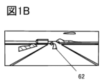
- FIG. 1A shows a schematic diagram of a display device having a curved surface.
- FIG. 1A shows an example of a display device 61G having a curved strip-shaped display area, which is provided in front of the user's head 60H. ).
- a flexible display is formed by providing a switching element or a light-emitting element on a flexible film.
- at least part of the display surface has a curved surface shape, specifically a belt shape, a cylindrical shape, or a hemispherical shape.
- the display surface can be arranged at least in front of the head.
- the display can be implemented using a device that secures to the user's nose or ear. Also, by combining a flexible display, it can be arranged not only in front of the head, but also on the side of the head, above the head, or behind the head.
- the display device When positioned on the side of the head, above the head, or behind the head, the display device is not limited to a device that secures to the user's nose or ears, but rather to a device that wraps around the user's head.
- a flexible display ie, a display screen with a large area, is placed in the front, so that a wide field of view or visible range is obtained.
- display is performed inside the space on the user side of the display device, and the rear surface of the display device is arranged on the side opposite to the user side of the display device.
- the user side of the display device may have a wide display area, or the display area of the display device may be made see-through so that only part of the mark is displayed.
- the image shown in FIG. 1(B) may be displayed with only the arrow mark 62 emitting light while the outside scenery remains as it is in the see-through area.
- the display device may be configured to have a first sensor unit for sensing the user's head on the user side, and an imaging device that generates a digital image that can realize the shape of the user's head in a three-dimensional space. can also be realized.
- a circuit for creating the image data In order to display a wide range of image based on image data obtained by a sensor unit provided on the user side of the display device, it is preferable to have a circuit for creating the image data.
- a second sensor section may be provided to sense information on the back side of the display device, that is, on the outside of the display device.
- a display having a curved surface can be arranged so as to surround the head, and the user's surroundings (area outside the display) can be displayed on the display having a curved surface.
- a curved display surface may be provided inside the display device so as to surround the user's head, and no display surface may be provided outside the display device. Further, it is not necessary to provide the second sensor unit for capturing an image of the surroundings outside the display device.
- the display device may be configured to have an audio output unit that outputs audio information.
- the load on the circuit for creating the image data may be reduced by lowering the display quality of the area that the user does not pay attention to.
- the screen display may be adjusted using foveated rendering using a first sensor unit that senses the line-of-sight position of the user inside the display device.
- Foveated rendering detects the line of sight of the user and partially changes the level of display quality, displaying a high-quality image in the area where the line of sight tends to be concentrated, and displaying a low-quality image in the surrounding area.
- An example includes displaying an image. Rendering with different image quality selectively based on the line of sight is also called a foveated rendering method.
- a display having a curved surface preferably has high definition, such as HD (1280 ⁇ 720 pixels), FHD (1920 ⁇ 1080 pixels), WQHD (2560 ⁇ 1440 pixels), WQXGA (2560 ⁇ 1600 pixels). ), 4K (3840 ⁇ 2160 pixels), 8K (7680 ⁇ 4320 pixels). In particular, it is preferable to set the resolution to 4K, 8K, or higher.
- the pixel density (definition) of the display device of one embodiment of the present invention is preferably 100 ppi or more, more preferably 300 ppi or more, more preferably 500 ppi or more, more preferably 1000 ppi or more, more preferably 2000 ppi or more, and 3000 ppi or more.
- the display device can correspond to various screen ratios by appropriately designing 1:1 (square), 4:3, 16:9, and 16:10.
- a device manufactured using a metal mask or FMM may be referred to as a device with an MM (metal mask) structure.
- a device fabricated without using a metal mask or FMM may be referred to as a device with an MML (metal maskless) structure.
- SBS ide By Side
- the material and structure can be optimized for each light-emitting device, so the degree of freedom in selecting the material and structure increases, and it becomes easy to improve luminance and reliability.
- a light-emitting device capable of emitting white light may be referred to as a white light-emitting device.
- a white light emitting device can be combined with a colored layer (for example, a color filter) to realize a full-color display device.
- light-emitting devices can be broadly classified into a single structure and a tandem structure.
- a single-structure device preferably has one light-emitting unit between a pair of electrodes, and the light-emitting unit preferably includes one or more light-emitting layers.
- the light-emitting layers may be selected such that the respective light-emitting colors of the two light-emitting layers are in a complementary color relationship. For example, by making the luminescent color of the first luminescent layer and the luminescent color of the second luminescent layer have a complementary color relationship, it is possible to obtain a configuration in which the entire light emitting device emits white light.
- the light-emitting device as a whole may emit white light by combining the respective light-emitting colors of the three or more light-emitting layers.
- a tandem structure device preferably has two or more light-emitting units between a pair of electrodes, and each light-emitting unit includes one or more light-emitting layers.
- each light-emitting unit includes one or more light-emitting layers.
- a structure in which white light emission is obtained by combining light from the light emitting layers of a plurality of light emitting units may be employed. Note that the structure for obtaining white light emission is the same as the structure of the single structure.
- an intermediate layer typified by a charge generation layer is preferably provided between the plurality of light emitting units.
- the white light emitting device when comparing the white light emitting device (single structure or tandem structure) and the light emitting device having the SBS structure, the light emitting device having the SBS structure can consume less power than the white light emitting device. If it is desired to keep power consumption low, it is preferable to use a light-emitting device with an SBS structure. On the other hand, the white light emitting device is preferable because the manufacturing process is simpler than that of the SBS structure light emitting device, so that the manufacturing cost can be lowered or the manufacturing yield can be increased.
- the distance between the light-emitting devices can be reduced.
- the distance between light-emitting devices, the distance between EL layers, or the distance between pixel electrodes is less than 10 ⁇ m, 5 ⁇ m or less, 3 ⁇ m or less, 2 ⁇ m or less, 1 ⁇ m or less, 500 nm or less, 200 nm or less, 100 nm or less, or 90 nm or less. , 70 nm or less, 50 nm or less, 30 nm or less, 20 nm or less, 15 nm or less, or 10 nm or less.
- the distance between the side surface of the first organic layer 112R and the side surface of the second organic layer 112G or the distance between the side surface of the second organic layer 112G and the side surface of the third organic layer 112B is 1 ⁇ m or less. It has a region, preferably a region of 0.5 ⁇ m (500 nm) or less, more preferably a region of 100 nm or less.
- a direct-view image display device can be used to achieve high resolution and a large screen.
- imaging devices it is possible to realize an imaging device that generates a digital image that can realize the shape of the user's head in a three-dimensional space. It is also possible to provide a data analysis system based on images of the user or driver.
- a foveated rendering method can be used to display an image that is optimal for the user.
- a three-dimensional model of the user's head can be formed by the first sensor unit.
- FIG. 1A is a schematic diagram showing the positional relationship between a display device and a user according to one embodiment of the present invention
- FIG. 1B is a diagram showing an example of a display image displayed in front
- FIG. 2A is a schematic diagram showing the positional relationship between a display device and a user according to one embodiment of the present invention
- FIG. 2B is an exploded view of the display device
- FIG. 2C is a part of a display image displayed in front.
- FIG. 2D is a diagram showing a portion of the display image displayed in the rear.
- FIG. 3A is a schematic diagram showing the positional relationship between a display device and a user, showing one embodiment of the present invention
- FIG. 3B is a variation thereof.
- FIG. 4A is a schematic diagram showing the positional relationship between a display device and a user according to one embodiment of the present invention
- FIG. 4B is an enlarged head view of FIG. 4A
- FIG. 4C is a side view thereof.
- FIG. 5A is a schematic diagram showing the positional relationship between a display device and a user according to one embodiment of the present invention
- FIG. 5B is an example of a flowchart of display on the display device according to one embodiment of the present invention.
- FIG. 6 shows an example of a flow diagram of display on a display device according to one embodiment of the present invention.
- 7A and 7B are schematic diagrams showing the positional relationship between a display device and a user, each showing one embodiment of the present invention.
- FIGS. 8A to 8C are diagrams showing configuration examples of a display device.
- 9A to 9F are diagrams showing configuration examples of pixels.
- FIG. 10 is a diagram illustrating a configuration example of a display device.
- 11A and 11B are diagrams showing configuration examples of a display device.
- 12A to 12F are diagrams showing configuration examples of light-emitting devices.
- 13A and 13B are diagrams showing configuration examples of light receiving devices.
- 13C to 13E are diagrams illustrating configuration examples of display devices.
- FIG. 1A shows an example of a display device 61G having a curved band-shaped display area, which is provided in front of the user's head 60H, and an example of the front display image is shown in FIG. 1B.
- the display device 61G is an example in which a curved band-shaped display area is formed by deforming one rectangular display panel using a lightweight and flexible film.
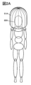
- FIG. 2A shows an example of a display device having a wider display area than the display device 61G of FIG. 1A.
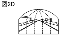
- FIG. 2A shows an example in which a display device 61A having a dome-shaped appearance that can be said to be a combination of a hemisphere and a cylinder is installed on the user's head 60H.
- the display device 61A has a hollow inside, in which the user's head 60H can be placed.
- a display surface, that is, a display area 63 is provided inside the display device 61A, that is, on the user side. By displaying an image, the display surface covers a wide range of the user's visual field and occupies the image display area.
- the display device 61A Since the display device 61A has a hollow inside, the user can move the neck and move the head 60H left, right, up and down. Since the display device 61A has a hollow inside, the display device can be seen while wearing glasses, and the display device 61A does not need to be fixed to the head 60H, so that the head 60H bears the weight of the display device. There is no Also, an optical system may be provided to adjust the distance between the user's eyes and the display area 63 as required. The distance between the user's eyes and the display area 63 is preferably 80 mm or more. If the distance is less than 80 mm, it is difficult to focus, so it is preferable to wear dedicated glasses for focusing.
- the installation method is not particularly limited as long as the display device 61A can be installed so that it can be placed over the user's head 60H. , or the display device 61A is hung from above the user.
- the user's head 60H lying on the table is covered, and a part of the user's head 60H is in contact with a part of the inner side of the display device 61A so that the image display is shown with the user lying down.
- the display device is fixed to a movable arm so that it can be used in the field of amusement, and the display device is moved so as to cover the user's head.
- a movable arm may be fixed to a training device such as a treadmill, and the display device may come in contact with the user's head while exercising.
- FIG. 2B shows an example of a developed view of a display panel used in the display device 61A.
- the display panel has a display area 63 and a non-display area 64 .
- the display area 63 is provided with a plurality of pixels (organic EL elements or LED elements) arranged in a matrix.
- an active matrix display device is manufactured using a flexible substrate.
- the non-display area 64 is provided with one or more of wirings, terminals, electrodes, and driving circuits (gate drivers or source drivers).
- An IC chip or FPC Flexible Printed Circuit
- a flexible film may be used to deform one large display panel to realize a dome-shaped image display area surrounding the user's head 60H.
- FIG. 2B shows an example in which one large display panel is deformed.
- An image display area surrounding the user's head 60H may be implemented.
- FIG. 2C shows an example of a display image in front of the user, which is a half area of the display area displayed inside the display device 61A.
- FIG. 2D shows an example of a display image behind the user, which is the remaining half of the display area displayed inside the display device 61A.
- the displayed images shown in FIGS. 1B and 2C are displayed by adding an arrow mark 62 to the image captured by the imaging camera.
- the display image is not limited to the arrow mark 62, and the display image may be processed by adding character information or guidelines.
- the display device 61A when the display device 61A is installed so as to be placed on the user's head 60H, the user side, that is, the display A touch input portion may be provided in the display area displayed to the user's eyes inside the device 61A. That is, a display panel that allows touch input may be used.
- the touch input unit can also be said to be a kind of first sensor unit. If the distance between the user's eyes and the display area 63 is such that the user's hands can be put into it, the user himself/herself can adjust the image in the display area displayed inside the display device 61A. Image adjustment shall include eye level adjustment, brightness adjustment, or chromaticity adjustment.
- the second sensor section is placed on the opposite side of the user, that is, on the outside of the display device 61A so that the display device 61A can be placed over the user's head 60H so as not to cause a sense of discomfort immediately after the display device 61A is installed. may be provided to display the image of the surroundings. In this way, before and after the display device 61A is installed on the user's head 60H, the image is almost the same as the image around the user, thereby giving the user a sense of security and adjusting the appearance of the image. can be done. These are useful when the display device 61A is used as part of an amusement park attraction.
- a display device 61A is set on the head 60H before the attraction, and a display image is gradually changed from a realistic surrounding image to an image of an unreal space reflecting the contents of the attraction, thereby giving a sense of immersion. can be done. Further, in order to detect motion sickness of the user or abnormality of the user, a camera for detecting a line of sight or a sensor for measuring body temperature may be provided inside the display device 61A as the first sensor section. In addition, when the user wants to stop the attraction, the user can make an emergency stop by touch input on the inner display panel. For example, it is possible to detect the movement of the hand and to make an emergency stop, so that the attraction can be made safer.
- the display device 61A can be installed in the training machine and used by the user.
- the weight is placed on the neck, so it is difficult to continue exercising while wearing the head-mounted display.
- even a slight movement of the neck causes the image to change abruptly based on the acceleration sensor, so motion sickness is likely to occur.
- the display device 61A is hollow, and even if the user moves the neck left or right, the image in the direction of the movement is already displayed.
- an imaging element may be provided as a first sensor section inside the display device 61A, and an automatic stop function may be provided for emergency stop when detecting a facial expression or an abnormality of the face.
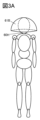
- the shape of the display device 61A is not limited, and may be a hemispherical shape (also referred to as a hemispherical shape) illustrated in FIG. 3A or a cylindrical shape (also referred to as a cylindrical shape) illustrated in FIG. 3B.
- the display device 61B has a shape in which a part of the user's head 60H is not covered, and since the user's mouth is open, the user can speak without being muffled. Moreover, the display device 61B can also be made lighter. In addition, the flexible display is lightweight, and if it is not provided with an optical system, it can be configured so that it does not feel heavy even if it is fixed to the top of the user's head.
- the display device 61C has a cylindrical shape, so it is easier to design than other configurations having a hemisphere in part. It can be assembled by combining another circular flat display on top.
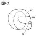
- FIG. 4A A helmet-type display device shown in FIG. 4A may also be used.
- FIG. 4B shows a front view and
- FIG. 4C shows a side view.
- the display device is an example in which a display device 61D having an appearance of a helmet and having a display area inside is combined with a see-through display device 61E capable of displaying an image on a window for viewing the outside.
- a flexible display is fixed to the curved surface of a translucent member so that the user can see the surroundings.
- the navigation system can be used to guide the driver even in bad weather, such as rain.
- a microphone for voice input may be equipped as a first sensor unit inside the helmet-type display device shown in FIG. It is also possible to enable operation by line-of-sight input.
- the second sensor section for capturing an image of the rear on the outside of the helmet-type display device, it is possible to display the rearward image in part of the display area inside the helmet.
- a user riding a two-wheeled vehicle typified by a motorcycle or an automobile can install a helmet-type display device on the head 60H.
- a user who works in a dangerous workplace can install a helmet-type display device on the head 60H.
- the helmet-type display device has a display area inside a shell portion made of a material having strength to protect the head 60H.
- FIG. 5A shows a side view of an arch-shaped display device 61F placed over the user's head 60H.
- the display device 61F is not particularly limited as long as it can be installed so that it can be placed over the user's head 60H.
- the display device 61F is used by fixing it to the upper half of the body, or by hanging it from above the user.
- the user's head 60H lying on the table is covered, and a part of the user's head 60H is in contact with a part of the inner side of the display device 61F so that the image display is shown with the user lying down.
- the display device is fixed to a movable arm and moved so as to cover the user's head.
- the display device 61F has an image processing circuit inside, and a display area and a first sensor section on the user side.
- the display device 61F has a second sensor section that captures an image of the front and a third sensor section that captures an image of the rear.
- FIG. 5B shows an example of a flow chart of display on the display device 61F.
- the image processing circuit is used to create data for displaying the forward image. conduct.
- the obtained data is displayed in the inner display area of the display device 61F.
- the forward image is displayed inside the display device.
- the line of sight is detected by the first sensor provided inside the display device 61F.
- the forward image display displayed inside the display device 61F is corrected or adjusted (including foveated rendering).
- the scale of the displayed image may be adjusted based on the line-of-sight detection data.
- the image processing circuit is used to create data for displaying the rear image.
- the front image display and the rear image display are displayed side by side inside the display device 61F.
- the front image display area and the rear image display area are displayed side by side.
- the rear image display area is displayed with high definition, and the front image display area is displayed with low definition. Further, when the user focuses on the front image display area, the front image display area is displayed with high definition, and the rear image display area is displayed with low definition. It is also possible to reduce power consumption by lowering the definition of areas other than the focused display area.
- FIG. 5A shows an example in which one flexible display is curved in a U shape, and both sides are open. may be configured.
- an imaging device that generates a digital image that can realize the shape of the user's head 60H in a three-dimensional space by installing the first sensor units in four directions. It is also possible to provide a data analysis system based on detailed 3D image data of the user's or driver's head 60H.
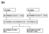
- FIG. 6 shows another example of the flow chart of the display on the display device 61F.
- the second sensor unit for capturing an image of the front of the display device 61F captures an image of the front
- the third sensor that captures an image of the rear of the display device 61F captures an image of the rear, and each data is created.
- the front image display and the rear image display are arranged side by side to synthesize a display image. If the mounting position or performance of the second sensor unit and the third sensor unit are different, an image processing circuit is used to align the front image display and the rear image display so that the height of the surrounding scenery is the same, and 360 degrees It is possible to display an omnidirectional display image inside the display device 61F by synthesizing the panoramic images.
- the front image display is displayed inside the display device 61F as required by the user.
- the present embodiment is not limited to the display device 61F, and can be applied to the display devices 61A, 61B, 61C, 61D, 61E, and 61G shown in the first embodiment.
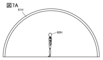
- FIG. 7A shows an example of a schematic cross-sectional view of a large display device 61H.
- the large display device 61H is used in a large-scale park represented by an amusement facility, and is configured to accommodate a large number of people inside the large display device 61H.
- the large display device 61H can be applied to planetariums, for example.
- FIG. 7A shows an example of one user.
- the large display device 61H has a hemispherical display area, and the display area of the display device 61H is installed in front of the user's head 60H even when the user moves or turns.
- the display area of the display device 61H is configured by combining flexible displays having curved surfaces and surrounding the user with the flexible displays on all four sides. Therefore, since the display area of the display device 61H is set around the user, the user can get a sense of immersion.
- the display device 61J is not limited to a hemispherical shape having a curved surface on the entire surface, and may be a display device 61J having an internal space that is a closed space composed of a flat surface and a curved surface as shown in FIG. 7B.
- the four sides of the user are configured by combining a flexible display and a flat display.
- FIG. 7B is a schematic cross-sectional view of the display device 61J.
- the display device 61J has a display area with a U-shaped cross section, and the display area of the display device 61J is installed in front of the user's head 60H even when the user moves or turns. Therefore, since the display area of the display device 61J is set around the user, the user can get a sense of immersion.
- a display device 61J of a simulation device or a game device used in an amusement facility or an experience facility is configured to accommodate one person or several persons.
- the entrance for entering the inside of the display device 61H or the display device 61J is an entrance that can be opened and closed, and a display area is also provided in that portion, the entire surface can be used as an area, but only the entrance is displayed as an emergency exit. It is also possible to adopt a configuration in which no region is used. Further, an entrance for entering the inside of the display device 61H or the display device 61J may be provided at the foot so that the user can move from below the display device 61H or the display device 61J using stairs or a tunnel from the outside.
- Embodiment 4 a structural example of a display device to which one embodiment of the present invention can be applied will be described.
- the display devices exemplified below are applied to any one of the display devices 61A, 61B, 61C, 61D, 61E, 61F, 61G, 61H, and 61J of Embodiments 1, 2, and 3. can do.
- One embodiment of the present invention is a display device including a light-emitting element (also referred to as a light-emitting device).
- a display device has two or more light-emitting elements that emit light of different colors. Each light-emitting element has a pair of electrodes and an EL layer therebetween.
- the light-emitting element is preferably an organic EL element (organic electroluminescence element). Two or more light-emitting elements that emit different colors have EL layers each containing a different light-emitting material.
- a full-color display device can be realized by using three types of light-emitting elements that emit red (R), green (G), and blue (B) light.
- island-like layers containing at least light-emitting materials with different emission colors.
- a method of forming an island-shaped organic film by a vapor deposition method using a shadow mask such as a metal mask is known.
- various influences such as the precision of the metal mask, the misalignment between the metal mask and the substrate, the bending of the metal mask, and the broadening of the contour of the film to be formed due to the scattering of vapor, etc. cause island-like organic films.
- the layer profile may be blurred and the edge thickness may be reduced.
- the thickness of the island-shaped light-emitting layer may vary depending on the location.
- countermeasures have been taken to artificially increase the definition (also called pixel density) by adopting a special pixel arrangement method such as a pentile arrangement.
- an island-shaped light-emitting layer means that the light-emitting layer is physically separated from an adjacent light-emitting layer.
- an EL layer is processed into a fine pattern by photolithography without using a shadow mask such as a fine metal mask (FMM).
- a shadow mask such as a fine metal mask (FMM).
- FMM fine metal mask
- the EL layers can be separately formed, a display device with extremely vivid, high contrast, and high display quality can be realized.
- the EL layer may be processed into a fine pattern using both a metal mask and photolithography.
- part or all of the EL layer can be physically separated. Accordingly, leakage current between light-emitting elements can be suppressed through a layer (also referred to as a common layer) used in common between adjacent light-emitting elements. Thereby, crosstalk due to unintended light emission can be prevented, and a display device with extremely high contrast can be realized. In particular, a display device with high current efficiency at low luminance can be realized.
- One embodiment of the present invention can also be a display device in which a light-emitting element that emits white light and a color filter are combined.
- light-emitting elements having the same structure can be applied to light-emitting elements provided in pixels (sub-pixels) that emit light of different colors, and all layers can be common layers. Further, part or all of each EL layer is divided by photolithography. As a result, leakage current through the common layer is suppressed, and a high-contrast display device can be realized.
- a device having a tandem structure in which a plurality of light-emitting layers are stacked via a highly conductive intermediate layer, it is possible to effectively prevent leakage current through the intermediate layer, resulting in high brightness and high definition. , and high contrast.
- an insulating layer covering at least the side surface of the island-shaped light emitting layer.
- the insulating layer may cover part of the top surface of the island-shaped EL layer.
- a material having barrier properties against water and oxygen is preferably used for the insulating layer.
- an inorganic insulating film that hardly diffuses water or oxygen can be used. Accordingly, deterioration of the EL layer can be suppressed, and a highly reliable display device can be realized.
- a phenomenon occurs in which the common electrode is divided by a step at the end of the EL layer (also referred to as step disconnection). may insulate. Therefore, it is preferable to adopt a structure in which a local step located between two adjacent light emitting elements is filled with a resin layer functioning as a planarization film (also called LFP: Local Filling Planarization).
- the resin layer has a function as a planarizing film.
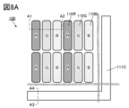
- FIG. 8A shows a schematic top view of the display device 100 of one embodiment of the present invention.
- the display device 100 includes, on a substrate 101, a plurality of light emitting elements 110R emitting red, light emitting elements 110G emitting green, and light emitting elements 110B emitting blue.
- the light emitting region of each light emitting element is labeled with R, G, and B. As shown in FIG.
- the light emitting elements 110R, 110G, and 110B are arranged in a matrix.
- FIG. 8A shows a so-called stripe arrangement in which light emitting elements of the same color are arranged in one direction.
- the arrangement method of the light-emitting elements is not limited to this, and an arrangement method represented by an S-stripe arrangement, a delta arrangement, a Bayer arrangement, and a zigzag arrangement may be applied, and a pentile arrangement and a diamond arrangement may also be used.
- the light emitting element 110R, the light emitting element 110G, and the light emitting element 110B for example, an OLED (Organic Light Emitting Diode) or a QLED (Quantum-dot Light Emitting Diode) is preferably used.
- the light-emitting substance that the EL element has include a substance that emits fluorescence (fluorescent material), a substance that emits phosphorescence (phosphorescent material), an inorganic compound (quantum dot material), and a substance that exhibits thermally activated delayed fluorescence (thermally activated delayed fluorescent (thermally activated delayed fluorescence: TADF) material).
- FIG. 8A also shows a connection electrode 111C electrically connected to the common electrode 113.
- FIG. 111 C of connection electrodes are given the electric potential (for example, anode electric potential or cathode electric potential) for supplying to the common electrode 113.
- FIG. The connection electrode 111C is provided outside the display area in which the light emitting elements 110R are arranged.
- connection electrodes 111C can be provided along the periphery of the display area. For example, it may be provided along one side of the periphery of the display area, or may be provided over two or more sides of the periphery of the display area. That is, when the top surface shape of the display area is rectangular, the top surface shape of the connection electrode 111C can be band-shaped (rectangular), L-shaped, U-shaped (square bracket-shaped), or square. .
- FIG. 8B and 8C are schematic cross-sectional views corresponding to the dashed-dotted line A1-A2 and the dashed-dotted line A3-A4 in FIG. 8A, respectively.
- FIG. 8B shows a schematic cross-sectional view of the light emitting elements 110R, 110G, and 110B
- FIG. 8C shows a schematic cross-sectional view of the connection portion 140 where the connection electrode 111C and the common electrode 113 are connected. ing.
- the light emitting element 110R has a pixel electrode 111R, a first organic layer 112R, a common layer 114, and a common electrode 113.
- the light emitting element 110G has a pixel electrode 111G, a second organic layer 112G, a common layer 114, and a common electrode 113.
- the light emitting element 110B has a pixel electrode 111B, a third organic layer 112B, a common layer 114, and a common electrode 113.
- the common layer 114 and the common electrode 113 are commonly provided for the light emitting elements 110R, 110G, and 110B.
- the first organic layer 112R of the light-emitting element 110R contains a light-emitting organic compound that emits light having an intensity in at least the red wavelength range.
- the second organic layer 112G included in the light-emitting element 110G includes a light-emitting organic compound that emits light having an intensity in at least the green wavelength range.
- the third organic layer 112B included in the light-emitting element 110B contains a light-emitting organic compound that emits light having an intensity in at least a blue wavelength range.
- Each of the first organic layer 112R, the second organic layer 112G, and the third organic layer 112B can also be called an EL layer and includes at least a layer containing a light-emitting organic compound (light-emitting layer).
- the light-emitting element 110R, the light-emitting element 110G, and the light-emitting element 110B may be referred to as the light-emitting element 110 when describing matters common to them.
- the letters are omitted when describing matters common to these. Reference numerals may be used to refer to the organic layer 112 in some cases.
- the organic layer 112 and the common layer 114 may each independently have one or more of an electron injection layer, an electron transport layer, a hole injection layer, and a hole transport layer.
- the organic layer 112 may have a layered structure of a hole injection layer, a hole transport layer, a light emitting layer, and an electron transport layer from the pixel electrode 111 side, and the common layer 114 may have an electron injection layer. .
- a pixel electrode 111R, a pixel electrode 111G, and a pixel electrode 111B are provided for each light emitting element.
- the common electrode 113 and the common layer 114 are provided as a continuous layer common to each light emitting element.
- a conductive film having a property of transmitting visible light is used for one of the pixel electrodes and the common electrode 113, and a conductive film having a reflective property is used for the other.
- a protective layer 121 is provided on the common electrode 113 to cover the light emitting elements 110R, 110G, and 110B.
- the protective layer 121 has a function of preventing impurities typified by water from diffusing into each light-emitting element from above.
- the end of the pixel electrode 111 preferably has a tapered shape.
- the portion of the organic layer 112 provided along the side surface of the pixel electrode also has a tapered shape.
- the side surface of the pixel electrode is tapered because foreign matter (for example, also referred to as dust or particles) in the manufacturing process can be easily removed by cleaning treatment.
- the tapered shape refers to a shape in which at least a part of the side surface of the structure is inclined with respect to the substrate surface.
- the organic layer 112 is processed into an island shape by photolithography. Therefore, the organic layer 112 has a shape in which the angle formed by the top surface and the side surface is close to 90 degrees at the end.
- an organic film formed using FMM Fe Metal Mask
- FMM Fe Metal Mask
- An insulating layer 125, a resin layer 126, and a layer 128 are provided between two adjacent light emitting elements.
- the resin layer 126 is positioned between two adjacent light emitting elements, and is provided so as to fill the end portions of the respective organic layers 112 and the area between the two organic layers 112 .
- the resin layer 126 has a smooth convex upper surface, and a common layer 114 and a common electrode 113 are provided to cover the upper surface of the resin layer 126 .
- the resin layer 126 functions as a flattening film that fills the steps located between the two adjacent light emitting elements. By providing the resin layer 126, a phenomenon in which the common electrode 113 is divided by a step at the end of the organic layer 112 (also referred to as step disconnection) occurs, and the common electrode on the organic layer 112 is prevented from being insulated. be able to.
- the resin layer 126 can also be called LFP (Local Filling Planarization).
- An insulating layer containing an organic material can be suitably used as the resin layer 126 .
- acrylic resin, polyimide resin, epoxy resin, imide resin, polyamide resin, polyimideamide resin, silicone resin, siloxane resin, benzocyclobutene-based resin, phenolic resin, and precursors of these resins are used as the resin layer 126.
- an organic material such as polyvinyl alcohol (PVA), polyvinyl butyral, polyvinylpyrrolidone, polyethylene glycol, polyglycerin, pullulan, water-soluble cellulose, or alcohol-soluble polyamide resin may be used.
- a photosensitive resin can be used as the resin layer 126 .
- a photoresist may be used as the photosensitive resin.
- a positive material or a negative material can be used for the photosensitive resin.
- the resin layer 126 may contain a material that absorbs visible light.
- the resin layer 126 itself may be made of a material that absorbs visible light, or the resin layer 126 may contain a pigment that absorbs visible light.
- the insulating layer 125 is provided in contact with the side surface of the organic layer 112 . Also, the insulating layer 125 is provided to cover the upper end portion of the organic layer 112 . A part of the insulating layer 125 is provided in contact with the upper surface of the substrate 101 .
- the insulating layer 125 is positioned between the resin layer 126 and the organic layer 112 and functions as a protective film to prevent the resin layer 126 from contacting the organic layer 112 .
- the organic layer 112 and the resin layer 126 are in contact with each other, the organic layer 112 may be dissolved by the organic solvent used when forming the resin layer 126 . Therefore, by providing the insulating layer 125 between the organic layer 112 and the resin layer 126 as shown in this embodiment mode, the side surface of the organic layer can be protected.
- the insulating layer 125 can be an insulating layer containing an inorganic material.
- an inorganic insulating film typified by an oxide insulating film, a nitride insulating film, an oxynitride insulating film, and a nitride oxide insulating film can be used, for example.
- the insulating layer 125 may have a single-layer structure or a laminated structure.
- the oxide insulating film includes a silicon oxide film, an aluminum oxide film, a magnesium oxide film, an indium gallium zinc oxide film, a gallium oxide film, a germanium oxide film, an yttrium oxide film, a zirconium oxide film, a lanthanum oxide film, a neodymium oxide film, and an oxide film.
- Examples include hafnium films and tantalum oxide films.
- Examples of the nitride insulating film include a silicon nitride film and an aluminum nitride film.
- Examples of the oxynitride insulating film include a silicon oxynitride film and an aluminum oxynitride film.
- nitride oxide insulating film examples include a silicon nitride oxide film and an aluminum nitride oxide film.
- a metal oxide film typified by a hafnium oxide film, or an inorganic insulating film typified by a silicon oxide film to the insulating layer 125, pinholes can be reduced and the EL layer can be formed.
- An insulating layer 125 having an excellent protective function can be formed.
- oxynitride refers to a material whose composition contains more oxygen than nitrogen
- nitride oxide refers to a material whose composition contains more nitrogen than oxygen.
- silicon oxynitride refers to a material whose composition contains more oxygen than nitrogen
- silicon nitride oxide refers to a material whose composition contains more nitrogen than oxygen.
- a sputtering method, a CVD method, a PLD method, or an ALD method can be used to form the insulating layer 125 .
- the insulating layer 125 is preferably formed by an ALD method with good coverage.
- a reflective film for example, a metal film containing one or more selected from silver, palladium, copper, titanium, and aluminum
- a reflective film is provided between the insulating layer 125 and the resin layer 126, and light is emitted from the light emitting layer.
- the reflected light may be reflected by the reflecting film.
- the layer 128 is part of a protective layer (also referred to as a mask layer or a sacrificial layer) for protecting the organic layer 112 when the organic layer 112 is etched.
- a protective layer also referred to as a mask layer or a sacrificial layer
- any of the materials that can be used for the insulating layer 125 can be used.
- an aluminum oxide film formed by ALD a metal oxide film typified by hafnium oxide, or an inorganic insulating film typified by silicon oxide has few pinholes. 125 and layer 128 can be suitably used.
- a protective layer 121 is provided to cover the common electrode 113 .
- the protective layer 121 can have, for example, a single layer structure or a laminated structure including at least an inorganic insulating film.
- inorganic insulating films include oxide films and oxynitride films typified by silicon oxide films, silicon oxynitride films, silicon nitride oxide films, silicon nitride films, aluminum oxide films, aluminum oxynitride films, and hafnium oxide films. , a nitride oxide film, or a nitride film.
- a semiconductor material or a conductive material typified by indium gallium oxide, indium zinc oxide, indium tin oxide, or indium gallium zinc oxide may be used for the protective layer 121 .
- a laminated film of an inorganic insulating film and an organic insulating film can also be used as the protective layer 121 .
- a structure in which an organic insulating film is sandwiched between a pair of inorganic insulating films is preferable.
- the organic insulating film functions as a planarizing film.
- the upper surface of the organic insulating film can be flattened, so that the coverage of the inorganic insulating film thereon can be improved, and the barrier property can be enhanced.
- the upper surface of the protective layer 121 is flat, when a structure (for example, a color filter, an electrode of a touch sensor, or a lens array) is provided above the protective layer 121, the influence of the uneven shape caused by the structure below can be reduced, which is preferable.
- a structure for example, a color filter, an electrode of a touch sensor, or a lens array
- FIG. 8C shows a connection portion 140 where the connection electrode 111C and the common electrode 113 are electrically connected.
- the connecting portion 140 an opening is provided in the insulating layer 125 and the resin layer 126 above the connecting electrode 111C.
- the connection electrode 111C and the common electrode 113 are electrically connected through the opening.
- FIG. 8C shows the connection portion 140 where the connection electrode 111C and the common electrode 113 are electrically connected. good. Especially when a carrier injection layer is used for the common layer 114, the electrical resistivity of the material used for the common layer 114 is sufficiently low and the thickness can be made thin. is often no problem. As a result, the common electrode 113 and the common layer 114 can be formed using the same shielding mask, so the manufacturing cost can be reduced.
- FIG. 8A A pixel layout different from that in FIG. 8A will be mainly described below.
- the arrangement of the light emitting elements (sub-pixels) is not particularly limited, and various methods can be applied.
- top surface shapes of sub-pixels include triangles, quadrilaterals (including rectangles and squares), polygons represented by pentagons, polygons with rounded corners, ellipses, and circles.
- the top surface shape of the sub-pixel corresponds to the top surface shape of the light emitting region of the light emitting element.
- the S-stripe arrangement is applied to the pixels 150 shown in FIG. 9A.
- the pixel 150 shown in FIG. 9A is composed of three sub-pixels, light emitting elements 110a, 110b and 110c.
- the light emitting element 110a may be a blue light emitting element
- the light emitting element 110b may be a red light emitting element
- the light emitting element 110c may be a green light emitting element.
- the pixel 150 shown in FIG. 9B includes a light emitting element 110a having a substantially trapezoidal top surface shape with rounded corners, a light emitting element 110b having a substantially triangular top surface shape with rounded corners, and a substantially square or substantially hexagonal top surface shape with rounded corners. and a light emitting element 110c having Further, the light emitting element 110a has a larger light emitting area than the light emitting element 110b. Thus, the shape and size of each light emitting element can be determined independently. For example, a more reliable light-emitting element can be made smaller.
- the light emitting element 110a may be a green light emitting element
- the light emitting element 110b may be a red light emitting element
- the light emitting element 110c may be a blue light emitting element.
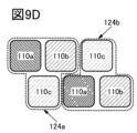
- FIG. 9C shows an example in which pixels 124a having light-emitting elements 110a and 110b and pixels 124b having light-emitting elements 110b and 110c are alternately arranged.
- the light emitting element 110a may be a red light emitting element
- the light emitting element 110b may be a green light emitting element
- the light emitting element 110c may be a blue light emitting element.
- the pixel 124a has two light emitting elements (light emitting elements 110a and 110b) in the upper row (first row) and one light emitting element (light emitting element 110c) in the lower row (second row).
- the pixel 124b has one light emitting element (light emitting element 110c) in the upper row (first row) and two light emitting elements (light emitting elements 110a and 110b) in the lower row (second row).
- the light emitting element 110a may be a red light emitting element
- the light emitting element 110b may be a green light emitting element
- the light emitting element 110c may be a blue light emitting element.
- FIG. 9D is an example in which each light emitting element has a substantially square top surface shape with rounded corners
- FIG. 9E is an example in which each light emitting element has a circular top surface shape.
- FIG. 9F is an example in which light emitting elements of each color are arranged in a zigzag pattern. Specifically, when viewed from above, the upper sides of two light emitting elements (for example, light emitting elements 110a and 110b, or light emitting elements 110b and 110c) aligned in the column direction are displaced.
- the light emitting element 110a may be a red light emitting element
- the light emitting element 110b may be a green light emitting element
- the light emitting element 110c may be a blue light emitting element.
- the top surface shape of the light emitting element may be a polygonal shape with rounded corners, an elliptical shape, or a circular shape.
- the EL layer is processed into an island shape using a resist mask.
- the resist film formed on the EL layer needs to be cured at a temperature lower than the heat resistance temperature of the EL layer. Therefore, curing of the resist film may be insufficient depending on the heat resistance temperature of the EL layer material and the curing temperature of the resist material.
- a resist film that is insufficiently hardened may take a shape away from the desired shape during processing.
- the top surface shape of the EL layer may be polygonal with rounded corners, elliptical, or circular. For example, when a resist mask having a square top surface is formed, a resist mask having a circular top surface is formed, and the EL layer may have a circular top surface.
- a technique for correcting the mask pattern in advance so that the design pattern and the transfer pattern match.
- OPC Optical Proximity Correction
- a correction pattern is added to the figure corner portion on the mask pattern.
- This embodiment can be implemented by appropriately combining at least part of it with other embodiments described herein.
- the display device of the present embodiment is, for example, a television device, a desktop or notebook personal computer, a computer monitor, a digital signage, or an electronic device having a relatively large screen such as a large game machine represented by a pachinko machine.
- it can be used for display parts of digital cameras, digital video cameras, digital photo frames, mobile phones, mobile game machines, smart phones, wristwatch terminals, tablet terminals, personal digital assistants, and sound reproducing devices.
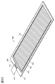
- FIG. 10 shows a perspective view of a display device 400 having an elongated rectangular shape (also referred to as a strip shape), and FIG. 11A shows a cross-sectional view of the display device 400. As shown in FIG.
- the display device 400 has a configuration in which a substrate 452 and a substrate 451 are bonded together.
- the substrate 452 is clearly indicated by dashed lines.
- the display device 61G having a curved band-shaped display area shown in FIG. 1 can be realized.
- the display device 400 has a display section 462 , a circuit 464 and wiring 465 .
- FIG. 10 shows an example in which an IC 473 and an FPC 472 are mounted on the display device 400 . Therefore, the configuration shown in FIG. 10 can also be called a display module including the display device 400, an IC (integrated circuit), and an FPC.
- a scanning line driving circuit for example, can be used as the circuit 464 .
- the wiring 465 has a function of supplying signals and power to the display section 462 and the circuit 464 .
- the signal and power are input to the wiring 465 from the outside through the FPC 472 or input to the wiring 465 from the IC 473 .
- FIG. 10 shows an example in which the IC 473 is provided on the substrate 451 by the COG (Chip On Glass) method or the COF (Chip on Film) method.
- the IC 473 for example, an IC having a scanning line driver circuit or a signal line driver circuit can be applied.
- the display device 400 and the display module may be configured without an IC.
- the IC may be mounted on the FPC by the COF method.
- FIG. 11A shows an example of a cross section of the display device 400 when part of the region including the FPC 472, part of the circuit 464, part of the display portion 462, and part of the region including the connection portion are cut. show.
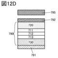
- FIG. 11A shows an example of a cross section of the display portion 462, in particular, a region including the light emitting element 430b that emits green light and the light emitting element 430c that emits blue light.
- a display device 400 illustrated in FIG. 11A includes a transistor 202, a transistor 210, a light-emitting element 430b, and a light-emitting element 430c between a substrate 451 and a substrate 452.
- the three sub-pixels are red (R), green (G), and blue (B).
- Color subpixels include three color subpixels: yellow (Y), cyan (C), and magenta (M).
- the four sub-pixels include R, G, B, and white (W) sub-pixels and R, G, B, and Y four-color sub-pixels. .
- the substrate 452 and the protective layer 416 are adhered via the adhesive layer 442 .
- the adhesive layer 442 is provided so as to overlap each of the light emitting elements 430b and 430c, and the display device 400 has a solid sealing structure.
- the light-emitting elements 430b and 430c have conductive layers 411a, 411b, and 411c as pixel electrodes.
- the conductive layer 411b reflects visible light and functions as a reflective electrode.
- the conductive layer 411c is transparent to visible light and functions as an optical adjustment layer.
- the conductive layer 411 a is connected to the conductive layer 222 b included in the transistor 210 through an opening provided in the insulating layer 214 .
- the transistor 210 has a function of controlling driving of the light emitting element.
- An EL layer 412G or an EL layer 412B is provided to cover the pixel electrodes.
- An insulating layer 421 is provided in contact with a side surface of the EL layer 412G and a side surface of the EL layer 412B, and a resin layer 422 is provided so as to fill recesses of the insulating layer 421.
- FIG. A layer 424 is provided between the EL layer 412G and the insulating layer 421 and between the EL layer 412B and the insulating layer 421, respectively.
- a common layer 414, a common electrode 413, and a protective layer 416 are provided to cover the EL layers 412G and 412B.
- the light emitted by the light emitting element is emitted to the substrate 452 side.
- a material having high visible light transmittance is preferably used for the substrate 452 .
- Both the transistor 202 and the transistor 210 are formed over the substrate 451 . These transistors can be made with the same material and the same process.
- the substrate 451 and the insulating layer 212 are bonded together by an adhesive layer 455 .
- a method for manufacturing the display device 400 first, a manufacturing substrate on which the insulating layer 212 , each transistor, and each light emitting element are provided and the substrate 452 are bonded together with an adhesive layer 442 . Then, the formation substrate is peeled off and a substrate 451 is attached to the exposed surface, so that each component formed over the formation substrate is transferred to the substrate 451 .
- a known method may be used as the peeling method or the transposing method.
- Each of the substrates 451 and 452 preferably has flexibility. Thereby, the flexibility of the display device 400 can be enhanced.
- an inorganic insulating film that can be used for the insulating layers 211 and 215 can be used.
- a connecting portion 204 is provided in a region of the substrate 451 where the substrate 452 does not overlap.
- the wiring 465 is electrically connected to the FPC 472 through the conductive layer 466 and the connection layer 242 .
- the conductive layer 466 can be obtained by processing the same conductive film as the pixel electrode. Thereby, the connecting portion 204 and the FPC 472 can be electrically connected via the connecting layer 242 .
- the transistor 202 and the transistor 210 each include a conductive layer 221 functioning as a gate, an insulating layer 211 functioning as a gate insulating layer, a semiconductor layer 231 having a channel formation region 231i and a pair of low-resistance regions 231n, and one of the pair of low-resistance regions 231n.
- a conductive layer 222a connected to a pair of low-resistance regions 231n, a conductive layer 222b connected to the other of a pair of low-resistance regions 231n, an insulating layer 225 functioning as a gate insulating layer, a conductive layer 223 functioning as a gate, and an insulating layer 215 covering the conductive layer 223 have
- the insulating layer 211 is located between the conductive layer 221 and the channel formation region 231i.
- the insulating layer 225 is located between the conductive layer 223 and the channel formation region 231i.
- the conductive layers 222a and 222b are each connected to the low resistance region 231n through openings provided in the insulating layer 215.
- One of the conductive layers 222a and 222b functions as a source and the other functions as a drain.
- FIG. 11A shows an example in which the insulating layer 225 covers the upper and side surfaces of the semiconductor layer.
- the conductive layers 222a and 222b are connected to the low-resistance region 231n through openings provided in the insulating layers 225 and 215, respectively.
- the insulating layer 225 overlaps the channel formation region 231i of the semiconductor layer 231 and does not overlap the low resistance region 231n.
- the structure shown in FIG. 11B can be manufactured by processing the insulating layer 225 using the conductive layer 223 as a mask.
- the insulating layer 215 is provided to cover the insulating layer 225 and the conductive layer 223, and the conductive layers 222a and 222b are connected to the low resistance regions 231n through openings in the insulating layer 215, respectively.
- an insulating layer 218 may be provided to cover the transistor.
- the structure of the transistor included in the display device of this embodiment There is no particular limitation on the structure of the transistor included in the display device of this embodiment.
- a planar transistor, a staggered transistor, or an inverted staggered transistor can be used.
- the transistor structure may be either a top-gate type or a bottom-gate type.
- gates may be provided above and below a semiconductor layer in which a channel is formed.
- a structure in which a semiconductor layer in which a channel is formed is sandwiched between two gates is applied to the transistors 202 and 210 .
- a transistor may be driven by connecting two gates and applying the same signal to them.
- the threshold voltage of the transistor may be controlled by applying a potential for controlling the threshold voltage to one of the two gates and applying a potential for driving to the other.
- the crystallinity of the semiconductor material used for the semiconductor layer of the transistor is not particularly limited, either.
- a semiconductor having a crystalline region in the semiconductor) may be used.
- a single crystal semiconductor or a crystalline semiconductor is preferably used because deterioration in transistor characteristics can be suppressed.
- a semiconductor layer of a transistor preferably includes a metal oxide (also referred to as an oxide semiconductor) exhibiting semiconductor characteristics.
- the display device of this embodiment preferably uses a transistor including a metal oxide for a channel formation region (hereinafter referred to as an OS transistor).
- the bandgap of the metal oxide used for the semiconductor layer of the transistor is preferably 2 eV or more, more preferably 2.5 eV or more.
- the metal oxide preferably contains at least indium or zinc, and more preferably contains indium and zinc.
- metal oxides include indium and M (where M is gallium, aluminum, yttrium, tin, silicon, boron, copper, vanadium, beryllium, titanium, iron, nickel, germanium, zirconium, molybdenum, lanthanum, cerium, neodymium). , hafnium, tantalum, tungsten, magnesium, and cobalt) and zinc.
- the semiconductor layer of the transistor may contain silicon.
- Silicon includes amorphous silicon and crystalline silicon (low temperature polysilicon or monocrystalline silicon).
- the transistor included in the circuit 464 and the transistor included in the display portion 462 may have the same structure or different structures.
- the plurality of transistors included in the circuit 464 may all have the same structure, or may have two or more types.
- the plurality of transistors included in the display portion 462 may all have the same structure, or may have two or more types.
- the insulating layer can function as a barrier layer. With such a structure, diffusion of impurities from the outside into the transistor can be effectively suppressed, and the reliability of the display device can be improved.
- Inorganic insulating films are preferably used as the insulating layer 211, the insulating layer 212, the insulating layer 215, the insulating layer 218, and the insulating layer 225, respectively.
- As the inorganic insulating film for example, a silicon nitride film, a silicon oxynitride film, a silicon oxide film, a silicon oxynitride film, an aluminum oxide film, and an aluminum nitride film can be used.
- a hafnium oxide film, an yttrium oxide film, a zirconium oxide film, a gallium oxide film, a tantalum oxide film, a magnesium oxide film, a lanthanum oxide film, a cerium oxide film, and a neodymium oxide film may be used.
- two or more of the inorganic insulating films described above may be laminated and used.
- An organic insulating film is suitable for the insulating layer 214 that functions as a planarizing layer.
- Materials that can be used for the organic insulating film include acrylic resins, polyimide resins, epoxy resins, polyamide resins, polyimideamide resins, siloxane resins, benzocyclobutene-based resins, phenolic resins, and precursors of these resins.
- optical members can be arranged along the inner or outer surface of the substrate 452 .
- optical members include a light shielding layer, a polarizing plate, a retardation plate, a light diffusion layer (diffusion film), an antireflection layer, a microlens array, and a light collecting film.
- an antistatic film that suppresses adhesion of dust, a water-repellent film that prevents adhesion of dirt, a hard coat film that suppresses the occurrence of scratches due to use, and a shock absorbing layer are arranged. good too.
- the protective layer 416 that covers the light-emitting element By providing the protective layer 416 that covers the light-emitting element, it is possible to prevent impurities such as water from entering the light-emitting element and improve the reliability of the light-emitting element.
- the connecting part 228 is shown in FIG. 11A. At the connecting portion 228, the common electrode 413 and the wiring are electrically connected.
- FIG. 11A shows an example in which the wiring has the same layered structure as the pixel electrode.
- Glass, quartz, ceramics, sapphire, resin, metal, alloy, and semiconductor can be used for the substrates 451 and 452, respectively.
- a material that transmits the light is used for the substrate on the side from which the light from the light-emitting element is extracted.
- the flexibility of the display device can be increased.
- a polarizing plate may be used as the substrate 451 or the substrate 452 .
- polyester resin represented by polyethylene terephthalate (PET) and polyethylene naphthalate (PEN), polyacrylonitrile resin, acrylic resin, polyimide resin, polymethyl methacrylate resin, polycarbonate (PC) resin, Polyethersulfone (PES) resin, polyamide resin (nylon, aramid), polysiloxane resin, cycloolefin resin, polystyrene resin, polyamideimide resin, polyurethane resin, polyvinyl chloride resin, polyvinylidene chloride resin, polypropylene resin, polytetrafluoro Ethylene (PTFE) resin, ABS resin, and cellulose nanofiber can be used.
- PET polyethylene terephthalate
- PEN polyethylene naphthalate
- PES Polyethersulfone
- polyamide resin nylon, aramid
- polysiloxane resin polystyrene resin
- polyamideimide resin polyurethane resin
- polyvinyl chloride resin polyvinylidene
- various curable adhesives represented by ultraviolet curable photocurable adhesives, reaction curable adhesives, thermosetting adhesives, and anaerobic adhesives can be used.
- These adhesives include epoxy resins, acrylic resins, silicone resins, phenol resins, polyimide resins, imide resins, PVC (polyvinyl chloride) resins, PVB (polyvinyl butyral) resins, and EVA (ethylene vinyl acetate) resins.
- epoxy resins with low moisture permeability are preferred.
- a two-liquid mixed type resin may be used.
- an adhesive sheet may be used.
- connection layer 242 an anisotropic conductive film (ACF) or an anisotropic conductive paste (ACP) can be used.
- ACF anisotropic conductive film
- ACP anisotropic conductive paste
- materials that can be used for conductive layers of various wirings and electrodes that constitute display devices include aluminum, titanium, chromium, nickel, copper, yttrium, zirconium, molybdenum, silver, and tantalum. , and metals represented by tungsten, and alloys containing these metals as main components. Films containing these materials can be used as a single layer or as a laminated structure.
- a conductive oxide typified by indium oxide, indium tin oxide, indium zinc oxide, zinc oxide, zinc oxide containing gallium, or graphene
- metal materials typified by gold, silver, platinum, magnesium, nickel, tungsten, chromium, molybdenum, iron, cobalt, copper, palladium, and titanium, or alloy materials containing such metal materials
- a nitride of the metal material eg, titanium nitride
- it is preferably thin enough to have translucency.
- a stacked film of any of the above materials can be used as the conductive layer.
- a laminated film of an alloy of silver and magnesium and indium tin oxide because the conductivity can be increased.
- These can also be used for a conductive layer typified by various wirings and electrodes forming a display device and a conductive layer (a conductive layer functioning as a pixel electrode or a common electrode) in a light-emitting element.
- Examples of insulating materials that can be used for each insulating layer include resins represented by acrylic resins and epoxy resins, and inorganic insulating materials represented by silicon oxides, silicon oxynitrides, silicon nitride oxides, silicon nitrides, and aluminum oxides. mentioned.
- This embodiment can be implemented by appropriately combining at least part of it with other embodiments described herein.
- Light-emitting devices can be broadly classified into single structures and tandem structures.
- a single structure device has one light emitting unit between a pair of electrodes.
- the light-emitting unit is configured to include one or more light-emitting layers.
- light-emitting layers may be selected such that the respective colors of light emitted from the two light-emitting layers are in a complementary color relationship. For example, in the case of two colors, by making the emission color of the first emission layer and the emission color of the second emission layer have a complementary color relationship, it is possible to obtain a configuration in which the entire light emitting device emits white light.
- the light-emitting device as a whole may emit white light by combining the respective light-emitting colors of the three or more light-emitting layers. The same applies to light-emitting devices having three or more light-emitting layers.
- a device with a tandem structure has a plurality of light-emitting units between a pair of electrodes.
- Each light-emitting unit is configured to include one or more light-emitting layers.
- luminance per predetermined current can be increased, and a light-emitting device with higher reliability than a single structure can be obtained.
- an intermediate layer typified by a charge generation layer is preferably provided between the plurality of light emitting units.
- the light emitting device with the SBS structure can consume less power than the white light emitting device.
- the manufacturing process of the white light emitting device is simpler than that of the SBS structure light emitting device, so that the manufacturing cost can be lowered and the manufacturing yield can be increased.
- the light emitting device has an EL layer 790 between a pair of electrodes (lower electrode 791, upper electrode 792).
- the EL layer 790 can be composed of a plurality of layers including the layer 720 , the light-emitting layer 711 , and the layer 730 .
- the layer 720 can have, for example, a layer containing a highly electron-injecting substance (electron-injecting layer) and a layer containing a highly electron-transporting substance (electron-transporting layer).
- the light-emitting layer 711 contains, for example, a light-emitting compound.
- Layer 730 can have, for example, a layer containing a highly hole-injecting substance (hole-injection layer) and a layer containing a highly hole-transporting substance (hole-transporting layer).
- a structure having a layer 720, a light-emitting layer 711, and a layer 730 provided between a pair of electrodes can function as a single light-emitting unit, and the structure of FIG. 12A is referred to herein as a single structure.
- the light emitting device shown in FIG. 12B has layers 730 - 1 , 730 - 2 , a light emitting layer 711 , layers 720 - 1 , 720 - 2 and an upper electrode 792 on the lower electrode 791 .
- the lower electrode 791 is the anode and the upper electrode 792 is the cathode.
- the layer 730-1 functions as a hole injection layer
- the layer 730-2 functions as a hole transport layer
- the layer 720-1 functions as an electron transport layer
- the layer 720-2 functions as an electron injection layer.
- the layer 730-1 is an electron injection layer
- the layer 730-2 is an electron transport layer
- the layer 720-1 is a hole transport layer
- the layer 720-2 is Each functions as a hole injection layer.
- a configuration in which a plurality of light-emitting layers (light-emitting layers 711, 712, and 713) are provided between layers 720 and 730 as shown in FIGS. 12C and 12D is also a variation of the single structure.
- tandem structure a structure in which a plurality of light-emitting units (EL layers 790a and 790b) are connected in series via an intermediate layer (charge generation layer) 740 is referred to as a tandem structure in this specification.
- a tandem structure may be called a stack structure. Note that the tandem structure enables a light-emitting device capable of emitting light with high luminance.
- the light-emitting layer 711, the light-emitting layer 712, and the light-emitting layer 713 may be made of a light-emitting material that emits light of the same color, or even the same light-emitting material. By stacking light-emitting layers, luminance can be increased.
- different light-emitting materials may be used for the light-emitting layers 711, 712, and 713.
- the light emitted from the light-emitting layer 711, the light-emitting layer 712, and the light-emitting layer 713 are complementary colors, white light emission can be obtained.
- FIG. 12D shows an example in which a colored layer 795 functioning as a color filter is provided. A desired color of light can be obtained by passing the white light through the color filter.
- light-emitting materials that emit light of the same color may be used for the light-emitting layer 711 and the light-emitting layer 712 .
- light-emitting materials that emit different light may be used for the light-emitting layer 711 and the light-emitting layer 712 .
- white light emission is obtained.
- FIG. 12F shows an example in which a colored layer 795 is further provided.
- the layer 720 and the layer 730 may have a laminated structure consisting of two or more layers as shown in FIG. 12B.
- light-emitting materials that emit light of the same color may be used for the light-emitting layers 711, 712, and 713.
- light-emitting materials that emit light of the same color may be used for light-emitting layer 711 and light-emitting layer 712 .
- a color conversion layer instead of the coloring layer 795, light of a desired color different from that of the light-emitting material can be obtained.
- a blue light-emitting material for each light-emitting layer and allowing blue light to pass through the color conversion layer, it is possible to obtain light having a longer wavelength than blue light (for example, red and green).
- a fluorescent material, a phosphorescent material, or quantum dots can be used as the color conversion layer.
- the emission color of the light-emitting device can be red, green, blue, cyan, magenta, yellow, or white depending on the material forming the EL layer 790 . Further, the color purity can be further enhanced by providing the light-emitting device with a microcavity structure.
- a light-emitting device that emits white light may have a structure in which a light-emitting layer contains two or more kinds of light-emitting substances, or two or more light-emitting layers having different light-emitting substances may be laminated. At this time, light-emitting substances may be selected so that the light emitted from each of the light-emitting substances has a complementary color relationship.
- a light-emitting device has at least a light-emitting layer. Further, in the light-emitting device, layers other than the light-emitting layer include a substance with high hole-injection property, a substance with high hole-transport property, a hole-blocking material, a substance with high electron-transport property, an electron-blocking material, and a layer with high electron-injection property. A layer containing a substance or a bipolar substance (a substance with high electron-transport and hole-transport properties) may be further included.
- Both low-molecular-weight compounds and high-molecular-weight compounds can be used in the light-emitting device, and inorganic compounds may be included.
- Each of the layers constituting the light-emitting device can be formed by vapor deposition (including vacuum vapor deposition), transfer, printing, inkjet, and coating.
- the light-emitting device may have one or more layers selected from a hole-injection layer, a hole-transport layer, a hole-blocking layer, an electron-blocking layer, an electron-transporting layer, and an electron-injecting layer, in addition to the light-emitting layer. can.
- the hole-injecting layer is a layer that injects holes from the anode to the hole-transporting layer, and contains a substance with high hole-injecting properties.
- Substances with a high hole-injecting property include aromatic amine compounds and composite materials containing a hole-transporting material and an acceptor material (electron-accepting material).
- the hole-transporting layer is a layer that transports holes injected from the anode to the light-emitting layer by means of the hole-injecting layer.
- a hole-transporting layer is a layer containing a hole-transporting material.
- the hole-transporting material a substance having a hole mobility of 1 ⁇ 10 ⁇ 6 cm 2 /Vs or more is preferable. Note that substances other than these can be used as long as they have a higher hole-transport property than electron-transport property.
- ⁇ -electron-rich heteroaromatic compounds e.g., carbazole derivatives, thiophene derivatives, furan derivatives
- aromatic amines compounds having an aromatic amine skeleton
- the electron-transporting layer is a layer that transports electrons injected from the cathode to the light-emitting layer by the electron-injecting layer.
- the electron-transporting layer is a layer containing an electron-transporting material.
- an electron-transporting material a substance having an electron mobility of 1 ⁇ 10 ⁇ 6 cm 2 /Vs or more is preferable. Note that substances other than these substances can be used as long as they have a higher electron-transport property than hole-transport property.
- electron-transporting materials include metal complexes having a quinoline skeleton, metal complexes having a benzoquinoline skeleton, metal complexes having an oxazole skeleton, metal complexes having a thiazole skeleton, oxadiazole derivatives, triazole derivatives, imidazole derivatives, and oxazole. derivatives, thiazole derivatives, phenanthroline derivatives, quinoline derivatives with quinoline ligands, benzoquinoline derivatives, quinoxaline derivatives, dibenzoquinoxaline derivatives, pyridine derivatives, bipyridine derivatives, pyrimidine derivatives, and other nitrogen-containing heteroaromatic compounds.
- a heteroaromatic compound having a high electron-transport property can be used.
- the electron injection layer is a layer that injects electrons from the cathode to the electron transport layer, and is a layer that contains a substance with high electron injection properties.
- Alkali metals, alkaline earth metals, or compounds thereof can be used as the substance with a high electron-injecting property.
- a composite material containing an electron-transporting material and a donor material (electron-donating material) can also be used as the substance with high electron-injecting properties.
- the electron injection layer examples include lithium, cesium, ytterbium, lithium fluoride (LiF), cesium fluoride (CsF), calcium fluoride (CaF 2 ), 8-(quinolinolato)lithium (abbreviation: Liq), 2- (2-pyridyl)phenoratritium (abbreviation: LiPP), 2-(2-pyridyl)-3-pyridinolatritium (abbreviation: LiPPy), 4-phenyl-2-(2-pyridyl)phenoratritium (abbreviation: LiPPy) LiPPP), lithium oxide (LiO x ), alkali metals such as cesium carbonate, alkaline earth metals, or compounds thereof can be used.
- the electron injection layer may have a laminated structure of two or more layers. As the laminated structure, for example, lithium fluoride can be used for the first layer and ytterbium can be used for the second layer.
- a material having an electron transport property may be used as the electron injection layer described above.
- a compound having a lone pair of electrons and an electron-deficient heteroaromatic ring can be used as the electron-transporting material.
- a compound having at least one of a pyridine ring, diazine ring (pyrimidine ring, pyrazine ring, pyridazine ring), and triazine ring can be used.
- the lowest unoccupied molecular orbital (LUMO) level of the organic compound having an unshared electron pair is preferably -3.6 eV or more and -2.3 eV or less.
- CV cyclic voltammetry
- photoelectron spectroscopy optical absorption spectroscopy
- inverse photoelectron spectroscopy are used to estimate the highest occupied molecular orbital (HOMO) level and LUMO level of an organic compound. be able to.
- BPhen 4,7-diphenyl-1,10-phenanthroline
- NBPhen 2,9-di(naphthalen-2-yl)-4,7-diphenyl-1,10-phenanthroline
- HATNA diquinoxalino [2,3-a:2′,3′-c]phenazine
- TmPPPyTz 2,4,6-tris[3′-(pyridin-3-yl)biphenyl-3-yl]-1,3 ,5-triazine
- TmPPPyTz 2,4,6-tris[3′-(pyridin-3-yl)biphenyl-3-yl]-1,3 ,5-triazine
- a light-emitting layer is a layer containing a light-emitting substance.
- the emissive layer can have one or more emissive materials.
- As the light-emitting substance a substance emitting blue, purple, blue-violet, green, yellow-green, yellow, orange, or red light is used as appropriate.
- a substance that emits near-infrared light can be used as the light-emitting substance.
- Luminous materials include fluorescent materials, phosphorescent materials, TADF materials, and quantum dot materials.
- fluorescent materials include pyrene derivatives, anthracene derivatives, triphenylene derivatives, fluorene derivatives, carbazole derivatives, dibenzothiophene derivatives, dibenzofuran derivatives, dibenzoquinoxaline derivatives, quinoxaline derivatives, pyridine derivatives, pyrimidine derivatives, phenanthrene derivatives, and naphthalene derivatives. .
- Examples of phosphorescent materials include organometallic complexes (especially iridium complexes) having a 4H-triazole skeleton, 1H-triazole skeleton, imidazole skeleton, pyrimidine skeleton, pyrazine skeleton, or pyridine skeleton, and phenylpyridine derivatives having an electron-withdrawing group.
- organometallic complexes especially iridium complexes
- platinum complexes, and rare earth metal complexes as ligands can be mentioned.
- the light-emitting layer may contain one or more organic compounds (host material, assist material) in addition to the light-emitting substance (guest material).
- One or both of a hole-transporting material and an electron-transporting material can be used as the one or more organic compounds.
- Bipolar materials or TADF materials may also be used as one or more organic compounds.
- the light-emitting layer preferably includes, for example, a phosphorescent material and a combination of a hole-transporting material and an electron-transporting material that easily form an exciplex.
- ExTET Exciplex-Triplet Energy Transfer
- a combination that forms an exciplex that emits light that overlaps with the wavelength of the absorption band on the lowest energy side of the light-emitting substance energy transfer becomes smooth and light emission can be efficiently obtained. With this configuration, high efficiency, low-voltage driving, and long life of the light-emitting device can be realized at the same time.
- This embodiment can be implemented by appropriately combining at least part of it with other embodiments described herein.
- a pn-type or pin-type photodiode can be used as the light receiving device.
- a light-receiving device functions as a photoelectric conversion device (also referred to as a photoelectric conversion element) that detects light incident on the light-receiving device and generates an electric charge. The amount of charge generated from the light receiving device is determined based on the amount of light incident on the light receiving device.
- organic photodiode having a layer containing an organic compound as the light receiving device.
- Organic photodiodes can be easily made thinner, lighter, and larger, and have a high degree of freedom in shape and design, so that they can be applied to various display devices.
- the light receiving device has a layer 765 between a pair of electrodes (lower electrode 761 and upper electrode 762).
- Layer 765 has at least one active layer and may have other layers.
- FIG. 13B is a modification of the layer 765 included in the light receiving device shown in FIG. 13A. Specifically, the light-receiving device shown in FIG. have.
- the active layer 767 functions as a photoelectric conversion layer.
- the layer 766 has one or both of a hole transport layer and an electron blocking layer.
- Layer 768 also includes one or both of an electron-transporting layer and a hole-blocking layer.
- a layer shared by the light-receiving device and the light-emitting device (which can be said to be a continuous layer shared by the light-receiving device and the light-emitting device) may exist.
- Such layers may have different functions in light-emitting devices than in light-receiving devices.
- Components are sometimes referred to herein based on their function in the light emitting device.
- a hole-injecting layer functions as a hole-injecting layer in light-emitting devices and as a hole-transporting layer in light-receiving devices.
- an electron-injecting layer functions as an electron-injecting layer in light-emitting devices and as an electron-transporting layer in light-receiving devices.
- a layer shared by the light-receiving device and the light-emitting device may have the same function in the light-emitting device as in the light-receiving device.
- a hole-transporting layer functions as a hole-transporting layer in both a light-emitting device and a light-receiving device
- an electron-transporting layer functions as an electron-transporting layer in both a light-emitting device and a light-receiving device.
- Both low-molecular-weight compounds and high-molecular-weight compounds can be used in the light-receiving device, and inorganic compounds may be included.
- the layers constituting the light-receiving device can be formed by a vapor deposition method (including a vacuum vapor deposition method), a transfer method, a printing method, an inkjet method, or a coating method.
- the active layer of the light receiving device contains a semiconductor.
- the semiconductor include inorganic semiconductors typified by silicon and organic semiconductors including organic compounds.
- an organic semiconductor is used as the semiconductor included in the active layer.
- the light-emitting layer and the active layer can be formed by the same method (for example, a vacuum deposition method), and a manufacturing apparatus can be shared, which is preferable.
- n-type semiconductor material of the active layer examples include fullerene (eg, C 60 , C 70 ) and electron-accepting organic semiconductor materials such as fullerene derivatives.
- fullerene derivatives include [6,6]-Phenyl-C71-butylic acid methyl ester (abbreviation: PC70BM), [6,6]-Phenyl-C61-butylic acid methyl ester (abbreviation: PC60BM), 1′, 1′′,4′,4′′-Tetrahydro-di[1,4]methanonaphthaleno[1,2:2′,3′,56,60:2′′,3′′][5,6]fullerene- C60 (abbreviation: ICBA) can be mentioned.
- n-type semiconductor material for example, perylenetetracarboxylic acid derivatives represented by N,N'-dimethyl-3,4,9,10-perylenetetracarboxylic acid diimide (abbreviation: Me-PTCDI), and , 2,2′-(5,5′-(thieno[3,2-b]thiophene-2,5-diyl)bis(thiophene-5,2-diyl))bis(methan-1-yl-1- ylidene)dimalononitrile (abbreviation: FT2TDMN).
- Me-PTCDI N,N'-dimethyl-3,4,9,10-perylenetetracarboxylic acid diimide
- FT2TDMN 2,2′-(5,5′-(thieno[3,2-b]thiophene-2,5-diyl)bis(thiophene-5,2-diyl)bis(methan-1-yl-1- ylidene
- Materials for the n-type semiconductor include metal complexes having a quinoline skeleton, metal complexes having a benzoquinoline skeleton, metal complexes having an oxazole skeleton, metal complexes having a thiazole skeleton, oxadiazole derivatives, triazole derivatives, imidazole derivatives, Oxazole derivatives, thiazole derivatives, phenanthroline derivatives, quinoline derivatives, benzoquinoline derivatives, quinoxaline derivatives, dibenzoquinoxaline derivatives, pyridine derivatives, bipyridine derivatives, pyrimidine derivatives, naphthalene derivatives, anthracene derivatives, coumarin derivatives, rhodamine derivatives, triazine derivatives, and quinones derivatives.
- Materials for the p-type semiconductor of the active layer include copper (II) phthalocyanine (CuPc), tetraphenyldibenzoperiflanthene (DBP), zinc phthalocyanine (ZnPc), and tin phthalocyanine. (SnPc), quinacridone, and rubrene electron-donating organic semiconductor materials.
- p-type semiconductor materials include carbazole derivatives, thiophene derivatives, furan derivatives, and compounds having an aromatic amine skeleton.
- materials for p-type semiconductors include naphthalene derivatives, anthracene derivatives, pyrene derivatives, triphenylene derivatives, fluorene derivatives, pyrrole derivatives, benzofuran derivatives, benzothiophene derivatives, indole derivatives, dibenzofuran derivatives, dibenzothiophene derivatives, indolocarbazole derivatives, porphyrin derivatives, phthalocyanine derivatives, naphthalocyanine derivatives, quinacridone derivatives, rubrene derivatives, tetracene derivatives, polyphenylenevinylene derivatives, polyparaphenylene derivatives, polyfluorene derivatives, polyvinylcarbazole derivatives, and polythiophene derivatives.
- the HOMO level of the electron-donating organic semiconductor material is preferably shallower (higher) than the HOMO level of the electron-accepting organic semiconductor material.
- the LUMO level of the electron-donating organic semiconductor material is preferably shallower (higher) than the LUMO level of the electron-accepting organic semiconductor material.
- a spherical fullerene as the electron-accepting organic semiconductor material, and use an organic semiconductor material with a shape close to a plane as the electron-donating organic semiconductor material. Molecules with similar shapes tend to gather together, and when molecules of the same type aggregate, the energy levels of the molecular orbitals are close to each other, so the carrier transportability can be enhanced.
- 6-diyl]-2,5-thiophenediyl[5,7-bis(2-ethylhexyl)-4,8-dioxo-4H,8H-benzo[1,2-c:4,5-c′]dithiophene-1 ,3-diyl]]polymer (abbreviation: PBDB-T) or a polymer compound represented by a PBDB-T derivative can be used.
- a method of dispersing an acceptor material in PBDB-T or a PBDB-T derivative can be used.
- the active layer is preferably formed by co-depositing an n-type semiconductor and a p-type semiconductor.
- the active layer may be formed by laminating an n-type semiconductor and a p-type semiconductor.
- three or more kinds of materials may be mixed in the active layer.
- a third material may be mixed in addition to the n-type semiconductor material and the p-type semiconductor material.
- the third material may be a low-molecular compound or a high-molecular compound.
- the light-receiving device further has a layer containing a highly hole-transporting substance, a highly electron-transporting substance, or a bipolar substance (substances with high electron-transporting and hole-transporting properties) as layers other than the active layer.
- the layer is not limited to the above, and may further include a layer containing a highly hole-injecting substance, a hole-blocking material, a highly electron-injecting substance, or an electron-blocking material.
- materials that can be used in the above-described light-emitting device can be used.
- a hole-transporting material or electron-blocking material a polymer compound represented by poly(3,4-ethylenedioxythiophene)/poly(styrenesulfonic acid) (PEDOT/PSS), and molybdenum oxide
- PEDOT/PSS poly(3,4-ethylenedioxythiophene)/poly(styrenesulfonic acid)
- molybdenum oxide An inorganic compound typified by copper iodide (CuI) can be used.
- Inorganic compounds typified by zinc oxide (ZnO) and organic compounds typified by polyethyleneimine ethoxylate (PEIE) can also be used as electron-transporting materials or hole-blocking materials.
- the light receiving device may have, for example, a mixed film of PEIE and ZnO.
- Display Device Having Photodetection Function
- light-emitting devices are arranged in matrix in the display portion, and an image can be displayed on the display portion.
- light receiving devices are arranged in a matrix in the display section, and the display section has one or both of an imaging function and a sensing function in addition to an image display function.
- the display part can be used for an image sensor or a touch sensor. That is, by detecting light on the display portion, an image can be captured, or proximity or contact of an object (a finger, hand, or pen) can be detected.
- the display device of one embodiment of the present invention can use the light-emitting device as a light source of the sensor portion.
- the light-receiving device can detect the reflected light (or scattered light).
- imaging or touch detection is possible.
- a display device of one embodiment of the present invention includes a light-emitting device and a light-receiving device in a pixel.
- a display device of one embodiment of the present invention uses an organic EL device as a light-emitting device and an organic photodiode as a light-receiving device.
- An organic EL device and an organic photodiode can be formed on the same substrate. Therefore, an organic photodiode can be incorporated in a display device using an organic EL device.
- a display device having a light-emitting device and a light-receiving device in a pixel, since the pixel has a light-receiving function, it is possible to detect contact or proximity of an object while displaying an image. For example, not only can an image be displayed by all the sub-pixels of the display device, but also some sub-pixels can emit light as a light source and the remaining sub-pixels can be used to display an image.
- the display device can capture an image using the light receiving device.
- the display device of this embodiment can be used as a scanner.
- an image sensor can be used to capture images for personal authentication using fingerprints, palm prints, irises, pulse shapes (including vein shapes and artery shapes), or faces.
- an image sensor can be used to capture an image around the eye, the surface of the eye, or the inside of the eye (fundus) of the user of the wearable device. Therefore, the wearable device can have a function of detecting any one or more selected from the user's blink, black eye movement, and eyelid movement.
- the light receiving device can be used as a touch sensor (also referred to as a direct touch sensor) or a near touch sensor (also referred to as a hover sensor, hover touch sensor, non-contact sensor, or touchless sensor).
- a touch sensor also referred to as a direct touch sensor
- a near touch sensor also referred to as a hover sensor, hover touch sensor, non-contact sensor, or touchless sensor.
- the touch sensor or near-touch sensor can detect the proximity or contact of an object (finger, hand, or pen).
- a touch sensor can detect an object by bringing the display device into direct contact with the object. Also, the near-touch sensor can detect the object even if the object does not touch the display device. For example, it is preferable that the display device can detect the object when the distance between the display device and the object is 0.1 mm or more and 300 mm or less, preferably 3 mm or more and 50 mm or less. With this structure, the display device can be operated without direct contact with the object, in other words, the display device can be operated without contact. With the above configuration, it is possible to reduce the risk of staining or scratching the display device, or to prevent the display device from directly touching the dirt (for example, dust or virus) attached to the display device by the object. can be operated.
- dirt for example, dust or virus
- the display device of one embodiment of the present invention can have a variable refresh rate.
- the power consumption can be reduced by adjusting the refresh rate (for example, in the range of 1 Hz to 240 Hz) according to the content displayed on the display device.
- the drive frequency of the touch sensor or the near-touch sensor may be changed according to the refresh rate. For example, when the refresh rate of the display device is 120 Hz, the driving frequency of the touch sensor or the near-touch sensor can be higher than 120 Hz (typically 240 Hz). With this structure, low power consumption can be achieved and the response speed of the touch sensor or the near touch sensor can be increased.
- the display device 100 shown in FIGS. 13C to 13E has a layer 353 having a light receiving device, a functional layer 355, and a layer 357 having a light emitting device between a substrate 351 and a substrate 359.
- FIG. 13A A layer 353 having a light receiving device, a functional layer 355, and a layer 357 having a light emitting device between a substrate 351 and a substrate 359.
- the functional layer 355 has a circuit for driving the light receiving device and a circuit for driving the light emitting device.
- One or more of switches, transistors, capacitors, resistors, wirings, and terminals can be provided in the functional layer 355 . Note that in the case of driving the light-emitting device and the light-receiving device by a passive matrix method, a structure in which the switch and the transistor are not provided may be employed.
- a finger 352 in contact with the display device 100 reflects light emitted by a light-emitting device in a layer 357 having a light-emitting device, so that a light-receiving device in a layer 353 having a light-receiving device reflects the light. Detect light. Thereby, it is possible to detect that the finger 352 touches the display device 100 .
- FIGS. 13D and 13E it may have a function of detecting or imaging an object that is close to (not in contact with) the display device.
- FIG. 13D shows an example of detecting a human finger
- FIG. 13E shows an example of detecting information (number of blinks, eye movement, eyelid movement) around, on the surface of, or inside the human eye.
- This embodiment can be implemented by appropriately combining at least part of it with other embodiments described herein.
- 61A head, 61A: display device, 61B: display device, 61C: display device, 61D: display device, 61E: display device, 61F: display device, 61G: display device, 61H: display device, 61J: display device, 62: arrow mark, 63: display area, 64: non-display area, 100: display device, 101: substrate, 110: light emitting element, 110a: light emitting element, 110b: light emitting element, 110B: light emitting element, 110c: light emitting element, 110G: light emitting element, 110R: light emitting element, 111: pixel electrode, 111B: pixel electrode, 111C: connection electrode, 111G: pixel electrode, 111R: pixel electrode, 112: organic layer, 112B: organic layer, 112G: organic layer, 112R: organic layer, 113: common electrode, 114: common layer, 121: protective layer, 124a: pixel, 124b: pixel, 125:
Landscapes
- Physics & Mathematics (AREA)
- Engineering & Computer Science (AREA)
- Multimedia (AREA)
- Signal Processing (AREA)
- General Physics & Mathematics (AREA)
- Optics & Photonics (AREA)
- Devices For Indicating Variable Information By Combining Individual Elements (AREA)
Priority Applications (4)
| Application Number | Priority Date | Filing Date | Title |
|---|---|---|---|
| JP2023563357A JPWO2023094945A1 (https=) | 2021-11-26 | 2022-11-17 | |
| US18/698,878 US20240414311A1 (en) | 2021-11-26 | 2022-11-17 | Display device |
| KR1020247019292A KR20240116475A (ko) | 2021-11-26 | 2022-11-17 | 표시 장치 |
| CN202280076426.8A CN118266206A (zh) | 2021-11-26 | 2022-11-17 | 显示装置 |
Applications Claiming Priority (2)
| Application Number | Priority Date | Filing Date | Title |
|---|---|---|---|
| JP2021-192241 | 2021-11-26 | ||
| JP2021192241 | 2021-11-26 |
Publications (1)
| Publication Number | Publication Date |
|---|---|
| WO2023094945A1 true WO2023094945A1 (ja) | 2023-06-01 |
Family
ID=86538914
Family Applications (1)
| Application Number | Title | Priority Date | Filing Date |
|---|---|---|---|
| PCT/IB2022/061053 Ceased WO2023094945A1 (ja) | 2021-11-26 | 2022-11-17 | 表示装置 |
Country Status (5)
| Country | Link |
|---|---|
| US (1) | US20240414311A1 (https=) |
| JP (1) | JPWO2023094945A1 (https=) |
| KR (1) | KR20240116475A (https=) |
| CN (1) | CN118266206A (https=) |
| WO (1) | WO2023094945A1 (https=) |
Citations (8)
| Publication number | Priority date | Publication date | Assignee | Title |
|---|---|---|---|---|
| JP2010256534A (ja) * | 2009-04-23 | 2010-11-11 | Fujifilm Corp | 全方位画像表示用ヘッドマウントディスプレイ装置 |
| JP2014219671A (ja) * | 2013-04-12 | 2014-11-20 | 株式会社半導体エネルギー研究所 | 表示装置 |
| JP2015172616A (ja) * | 2014-03-11 | 2015-10-01 | パナソニック株式会社 | ディスプレイ装置 |
| WO2016158080A1 (ja) * | 2015-03-30 | 2016-10-06 | ソニーセミコンダクタソリューションズ株式会社 | 情報処理装置、情報処理方法およびプログラム |
| CN205899143U (zh) * | 2016-07-20 | 2017-01-18 | 广东小天才科技有限公司 | 虚拟现实装置 |
| JP2019500633A (ja) * | 2015-10-26 | 2019-01-10 | グーグル エルエルシー | 複数のセグメントディスプレイおよび光学素子を備えたヘッドマウントディスプレイ装置 |
| US20190026871A1 (en) * | 2016-01-06 | 2019-01-24 | Samsung Electronics Co., Ltd. | Head-mounted electronic device |
| JP2020530971A (ja) * | 2017-06-14 | 2020-10-29 | チョン リ | ヘッドマウントディスプレイおよびそのディスプレイ画面、ヘッドマウントブラケットおよびビデオ |
Family Cites Families (46)
| Publication number | Priority date | Publication date | Assignee | Title |
|---|---|---|---|---|
| US20070069976A1 (en) * | 2005-09-26 | 2007-03-29 | Willins Bruce A | Method and system for interface between head mounted display and handheld device |
| US20090225001A1 (en) * | 2007-11-06 | 2009-09-10 | University Of Central Florida Research Foundation, Inc. | Hybrid Display Systems and Methods |
| JP5211667B2 (ja) * | 2007-12-07 | 2013-06-12 | ソニー株式会社 | 照明装置及び表示装置 |
| US8358317B2 (en) * | 2008-05-23 | 2013-01-22 | Evans & Sutherland Computer Corporation | System and method for displaying a planar image on a curved surface |
| US20100208029A1 (en) * | 2009-02-13 | 2010-08-19 | Samsung Electronics Co., Ltd | Mobile immersive display system |
| JP2010256769A (ja) * | 2009-04-28 | 2010-11-11 | Nippon Seiki Co Ltd | 発光表示装置 |
| KR101507206B1 (ko) * | 2012-02-13 | 2015-03-30 | 엘지디스플레이 주식회사 | 유연한 표시장치 |
| KR20140091100A (ko) * | 2012-12-26 | 2014-07-21 | 삼성디스플레이 주식회사 | 곡면 액정 표시 장치 |
| WO2014130458A1 (en) * | 2013-02-19 | 2014-08-28 | DreamLight Holdings Inc., formerly known as A Thousand Miles, LLC | Entertainment venue and associated systems/methods |
| WO2015038684A1 (en) * | 2013-09-10 | 2015-03-19 | Polyera Corporation | Attachable article with signaling, split display and messaging features |
| WO2015087498A1 (ja) * | 2013-12-11 | 2015-06-18 | パナソニック株式会社 | 表示装置 |
| EP2891919B1 (en) * | 2014-01-06 | 2021-02-17 | Samsung Electronics Co., Ltd | Bendable display apparatus |
| GB2526081A (en) * | 2014-05-08 | 2015-11-18 | Barco Nv | Curved projection screen |
| JP6823927B2 (ja) * | 2015-01-21 | 2021-02-03 | 株式会社半導体エネルギー研究所 | 表示システム |
| US10254795B2 (en) * | 2015-05-06 | 2019-04-09 | Flexterra, Inc. | Attachable, flexible display device with flexible tail |
| US10171768B2 (en) * | 2015-08-06 | 2019-01-01 | International Business Machines Corporation | Curve profile control for a flexible display |
| EP3268693A4 (en) * | 2015-08-19 | 2018-12-12 | Hyderabad Eye Research Foundation | An apparatus and a method therewith to quantify visual patterns in infants |
| CN108139804A (zh) * | 2015-10-15 | 2018-06-08 | 索尼公司 | 信息处理装置与信息处理方法 |
| EP3452991A4 (en) * | 2016-05-02 | 2020-01-08 | Warner Bros. Entertainment Inc. | GEOMETRY ADJUSTMENT IN VIRTUAL REALITY AND EXTENDED REALITY |
| JP2017215361A (ja) * | 2016-05-30 | 2017-12-07 | 三菱電機株式会社 | 表示装置 |
| US9858848B1 (en) * | 2016-06-09 | 2018-01-02 | International Business Machines Corporation | Dynamic display adjustment on a transparent flexible display |
| US20180088455A1 (en) * | 2016-09-23 | 2018-03-29 | L-3 Communications Corporation | Display system and components |
| US10921523B2 (en) * | 2016-09-23 | 2021-02-16 | L-3 Technologies, Inc. | Display system and components |
| KR20190076045A (ko) | 2016-11-10 | 2019-07-01 | 가부시키가이샤 한도오따이 에네루기 켄큐쇼 | 표시 장치 및 표시 장치의 구동 방법 |
| CN110637274B (zh) * | 2017-05-24 | 2022-05-03 | 索尼公司 | 信息处理设备、信息处理方法以及程序 |
| KR102505265B1 (ko) * | 2017-06-23 | 2023-03-06 | 삼성디스플레이 주식회사 | 전자 장치 |
| US20190037184A1 (en) * | 2017-07-28 | 2019-01-31 | Ravi Gauba | Projection Display Apparatus |
| GB201714297D0 (en) * | 2017-09-06 | 2017-10-18 | Flexenable Ltd | Curved display devices |
| CN107819073B (zh) * | 2017-10-26 | 2020-01-17 | 武汉华星光电半导体显示技术有限公司 | 基板及oled器件的制作方法 |
| US11188149B2 (en) * | 2018-02-09 | 2021-11-30 | University Of Fukui | Image display device using retinal scanning display unit and method thereof |
| US10726772B2 (en) * | 2018-05-29 | 2020-07-28 | Wuhan China Star Optoelectronics Technology Co., Ltd. | Display device, backlight module and manufacturing method thereof |
| US10861249B2 (en) * | 2018-07-27 | 2020-12-08 | The Q Digital Technologies, Inc. | Methods and system for manipulating digital assets on a three-dimensional viewing platform |
| US10852928B2 (en) * | 2018-12-14 | 2020-12-01 | Sony Corporation | Surface curvature control of display screen based on motion of support portions |
| KR102632543B1 (ko) * | 2019-02-19 | 2024-02-01 | 삼성디스플레이 주식회사 | 결합 부재를 포함하는 표시 장치 |
| CN109991778A (zh) * | 2019-04-11 | 2019-07-09 | 京东方科技集团股份有限公司 | 背光模组及显示设备 |
| USD1026099S1 (en) * | 2019-08-13 | 2024-05-07 | Aristocrat Technologies Australia Pty Limited | Gaming machine |
| CN114424110B (zh) * | 2019-08-30 | 2024-06-14 | 交互数字Vc控股公司 | 创建具有弹性光学层屈曲的3d多视图显示器 |
| CN113325620A (zh) * | 2020-02-28 | 2021-08-31 | 京东方科技集团股份有限公司 | 一种曲面车载显示模组、车载显示装置及车辆 |
| US11831454B2 (en) * | 2020-12-21 | 2023-11-28 | Christopher Max Schwitalla | Full dome conference |
| US11724173B2 (en) * | 2021-01-14 | 2023-08-15 | Supermax Simulation Inc. | System, method, and apparatus for providing an immersive experience for a sports or game simulation using a ball |
| US12044922B2 (en) * | 2021-05-11 | 2024-07-23 | Maven Optronics Co., Ltd. | Curved full-array LED light panel, curved backlight module and curved LCD |
| KR102693727B1 (ko) * | 2021-09-17 | 2024-08-09 | 주식회사 토비스 | 표시 장치 및 이의 제조 방법 |
| KR20230132021A (ko) * | 2022-03-07 | 2023-09-15 | 삼성디스플레이 주식회사 | 표시 장치 및 표시 장치의 제조방법 |
| CN114639713B (zh) * | 2022-03-30 | 2026-03-03 | 湖北长江新型显示产业创新中心有限公司 | 一种显示面板及显示装置 |
| US12020609B2 (en) * | 2022-05-04 | 2024-06-25 | Steven A. Welck | Immersive digital desktop display system |
| CN117769899A (zh) * | 2022-07-26 | 2024-03-26 | 京东方科技集团股份有限公司 | 显示装置 |
-
2022
- 2022-11-17 JP JP2023563357A patent/JPWO2023094945A1/ja active Pending
- 2022-11-17 KR KR1020247019292A patent/KR20240116475A/ko active Pending
- 2022-11-17 US US18/698,878 patent/US20240414311A1/en active Pending
- 2022-11-17 CN CN202280076426.8A patent/CN118266206A/zh active Pending
- 2022-11-17 WO PCT/IB2022/061053 patent/WO2023094945A1/ja not_active Ceased
Patent Citations (8)
| Publication number | Priority date | Publication date | Assignee | Title |
|---|---|---|---|---|
| JP2010256534A (ja) * | 2009-04-23 | 2010-11-11 | Fujifilm Corp | 全方位画像表示用ヘッドマウントディスプレイ装置 |
| JP2014219671A (ja) * | 2013-04-12 | 2014-11-20 | 株式会社半導体エネルギー研究所 | 表示装置 |
| JP2015172616A (ja) * | 2014-03-11 | 2015-10-01 | パナソニック株式会社 | ディスプレイ装置 |
| WO2016158080A1 (ja) * | 2015-03-30 | 2016-10-06 | ソニーセミコンダクタソリューションズ株式会社 | 情報処理装置、情報処理方法およびプログラム |
| JP2019500633A (ja) * | 2015-10-26 | 2019-01-10 | グーグル エルエルシー | 複数のセグメントディスプレイおよび光学素子を備えたヘッドマウントディスプレイ装置 |
| US20190026871A1 (en) * | 2016-01-06 | 2019-01-24 | Samsung Electronics Co., Ltd. | Head-mounted electronic device |
| CN205899143U (zh) * | 2016-07-20 | 2017-01-18 | 广东小天才科技有限公司 | 虚拟现实装置 |
| JP2020530971A (ja) * | 2017-06-14 | 2020-10-29 | チョン リ | ヘッドマウントディスプレイおよびそのディスプレイ画面、ヘッドマウントブラケットおよびビデオ |
Also Published As
| Publication number | Publication date |
|---|---|
| KR20240116475A (ko) | 2024-07-29 |
| US20240414311A1 (en) | 2024-12-12 |
| CN118266206A (zh) | 2024-06-28 |
| JPWO2023094945A1 (https=) | 2023-06-01 |
Similar Documents
| Publication | Publication Date | Title |
|---|---|---|
| WO2022175789A1 (ja) | 表示装置 | |
| JP7785086B2 (ja) | 遮光装置 | |
| JP2023056500A (ja) | 表示装置、表示モジュール、及び、電子機器 | |
| WO2022219455A1 (ja) | 表示装置、表示モジュール及び電子機器 | |
| US12342707B2 (en) | Display device and electronic device | |
| US20240334791A1 (en) | Display Apparatus And Electronic Device | |
| WO2023047235A1 (ja) | 表示装置の作製方法 | |
| WO2023285907A1 (ja) | 表示装置、表示モジュール、電子機器、及び、表示装置の作製方法 | |
| WO2022189878A1 (ja) | 表示装置、表示モジュール、電子機器、及び、表示装置の作製方法 | |
| US12586522B2 (en) | Correction method of display apparatus and correction system of the display apparatus | |
| US20240276833A1 (en) | Display device and display system | |
| JP7807450B2 (ja) | 表示装置、表示モジュール、及び電子機器 | |
| JP7823038B2 (ja) | 表示装置 | |
| US20240260373A1 (en) | Display apparatus, display module, and electronic device | |
| WO2023094945A1 (ja) | 表示装置 | |
| WO2023047239A1 (ja) | 表示装置 | |
| WO2023012577A1 (ja) | 表示装置 | |
| WO2023052913A1 (ja) | 表示装置 | |
| WO2023052892A1 (ja) | 表示装置、および電子機器 | |
| WO2023021360A1 (ja) | 表示装置、及び電子機器 | |
| WO2022224107A1 (ja) | 電子機器、および電子機器の認証方法 | |
| WO2023057855A1 (ja) | 表示装置、表示モジュール、及び、電子機器 | |
| WO2022180468A1 (ja) | 表示装置、表示モジュール、電子機器、及び、表示装置の作製方法 | |
| WO2022180482A1 (ja) | 表示装置、表示モジュール、電子機器、及び、表示装置の作製方法 | |
| US20240407225A1 (en) | Display apparatus |
Legal Events
| Date | Code | Title | Description |
|---|---|---|---|
| 121 | Ep: the epo has been informed by wipo that ep was designated in this application |
Ref document number: 22898031 Country of ref document: EP Kind code of ref document: A1 |
|
| WWE | Wipo information: entry into national phase |
Ref document number: 18698878 Country of ref document: US |
|
| ENP | Entry into the national phase |
Ref document number: 2023563357 Country of ref document: JP Kind code of ref document: A |
|
| WWE | Wipo information: entry into national phase |
Ref document number: 202280076426.8 Country of ref document: CN |
|
| ENP | Entry into the national phase |
Ref document number: 20247019292 Country of ref document: KR Kind code of ref document: A |
|
| NENP | Non-entry into the national phase |
Ref country code: DE |
|
| 122 | Ep: pct application non-entry in european phase |
Ref document number: 22898031 Country of ref document: EP Kind code of ref document: A1 |