WO2023090181A1 - 回路装置 - Google Patents
回路装置 Download PDFInfo
- Publication number
- WO2023090181A1 WO2023090181A1 PCT/JP2022/041328 JP2022041328W WO2023090181A1 WO 2023090181 A1 WO2023090181 A1 WO 2023090181A1 JP 2022041328 W JP2022041328 W JP 2022041328W WO 2023090181 A1 WO2023090181 A1 WO 2023090181A1
- Authority
- WO
- WIPO (PCT)
- Prior art keywords
- wiring
- capacitors
- coil
- circuit device
- current path
- Prior art date
- Legal status (The legal status is an assumption and is not a legal conclusion. Google has not performed a legal analysis and makes no representation as to the accuracy of the status listed.)
- Ceased
Links
Images


Classifications
-
- H—ELECTRICITY
- H03—ELECTRONIC CIRCUITRY
- H03H—IMPEDANCE NETWORKS, e.g. RESONANT CIRCUITS; RESONATORS
- H03H7/00—Multiple-port networks comprising only passive electrical elements as network components
- H03H7/01—Frequency selective two-port networks
- H03H7/0115—Frequency selective two-port networks comprising only inductors and capacitors
-
- H—ELECTRICITY
- H01—ELECTRIC ELEMENTS
- H01F—MAGNETS; INDUCTANCES; TRANSFORMERS; SELECTION OF MATERIALS FOR THEIR MAGNETIC PROPERTIES
- H01F17/00—Fixed inductances of the signal type
- H01F17/0006—Printed inductances
- H01F17/0013—Printed inductances with stacked layers
-
- H—ELECTRICITY
- H01—ELECTRIC ELEMENTS
- H01F—MAGNETS; INDUCTANCES; TRANSFORMERS; SELECTION OF MATERIALS FOR THEIR MAGNETIC PROPERTIES
- H01F27/00—Details of transformers or inductances, in general
- H01F27/06—Mounting, supporting or suspending transformers, reactors or choke coils not being of the signal type
-
- H—ELECTRICITY
- H01—ELECTRIC ELEMENTS
- H01F—MAGNETS; INDUCTANCES; TRANSFORMERS; SELECTION OF MATERIALS FOR THEIR MAGNETIC PROPERTIES
- H01F27/00—Details of transformers or inductances, in general
- H01F27/28—Coils; Windings; Conductive connections
- H01F27/29—Terminals; Tapping arrangements for signal inductances
- H01F27/292—Surface mounted devices
-
- H—ELECTRICITY
- H01—ELECTRIC ELEMENTS
- H01F—MAGNETS; INDUCTANCES; TRANSFORMERS; SELECTION OF MATERIALS FOR THEIR MAGNETIC PROPERTIES
- H01F27/00—Details of transformers or inductances, in general
- H01F27/40—Structural association with built-in electric component, e.g. fuse
-
- H—ELECTRICITY
- H01—ELECTRIC ELEMENTS
- H01G—CAPACITORS; CAPACITORS, RECTIFIERS, DETECTORS, SWITCHING DEVICES, LIGHT-SENSITIVE OR TEMPERATURE-SENSITIVE DEVICES OF THE ELECTROLYTIC TYPE
- H01G2/00—Details of capacitors not covered by a single one of groups H01G4/00-H01G11/00
- H01G2/02—Mountings
-
- H—ELECTRICITY
- H01—ELECTRIC ELEMENTS
- H01G—CAPACITORS; CAPACITORS, RECTIFIERS, DETECTORS, SWITCHING DEVICES, LIGHT-SENSITIVE OR TEMPERATURE-SENSITIVE DEVICES OF THE ELECTROLYTIC TYPE
- H01G4/00—Fixed capacitors; Processes of their manufacture
- H01G4/40—Structural combinations of fixed capacitors with other electric elements, the structure mainly consisting of a capacitor, e.g. RC combinations
-
- H—ELECTRICITY
- H03—ELECTRONIC CIRCUITRY
- H03H—IMPEDANCE NETWORKS, e.g. RESONANT CIRCUITS; RESONATORS
- H03H7/00—Multiple-port networks comprising only passive electrical elements as network components
- H03H7/01—Frequency selective two-port networks
-
- H—ELECTRICITY
- H03—ELECTRONIC CIRCUITRY
- H03H—IMPEDANCE NETWORKS, e.g. RESONANT CIRCUITS; RESONATORS
- H03H7/00—Multiple-port networks comprising only passive electrical elements as network components
- H03H7/01—Frequency selective two-port networks
- H03H7/09—Filters comprising mutual inductance
-
- H—ELECTRICITY
- H03—ELECTRONIC CIRCUITRY
- H03H—IMPEDANCE NETWORKS, e.g. RESONANT CIRCUITS; RESONATORS
- H03H7/00—Multiple-port networks comprising only passive electrical elements as network components
- H03H7/01—Frequency selective two-port networks
- H03H7/17—Structural details of sub-circuits of frequency selective networks
- H03H7/1741—Comprising typical LC combinations, irrespective of presence and location of additional resistors
- H03H7/1775—Parallel LC in shunt or branch path
-
- H—ELECTRICITY
- H01—ELECTRIC ELEMENTS
- H01F—MAGNETS; INDUCTANCES; TRANSFORMERS; SELECTION OF MATERIALS FOR THEIR MAGNETIC PROPERTIES
- H01F17/00—Fixed inductances of the signal type
- H01F17/0006—Printed inductances
- H01F17/0013—Printed inductances with stacked layers
- H01F2017/0026—Multilayer LC-filter
-
- H—ELECTRICITY
- H01—ELECTRIC ELEMENTS
- H01F—MAGNETS; INDUCTANCES; TRANSFORMERS; SELECTION OF MATERIALS FOR THEIR MAGNETIC PROPERTIES
- H01F27/00—Details of transformers or inductances, in general
- H01F27/06—Mounting, supporting or suspending transformers, reactors or choke coils not being of the signal type
- H01F2027/065—Mounting on printed circuit boards
-
- H—ELECTRICITY
- H03—ELECTRONIC CIRCUITRY
- H03H—IMPEDANCE NETWORKS, e.g. RESONANT CIRCUITS; RESONATORS
- H03H1/00—Constructional details of impedance networks whose electrical mode of operation is not specified or applicable to more than one type of network
- H03H1/0007—Constructional details of impedance networks whose electrical mode of operation is not specified or applicable to more than one type of network of radio frequency interference filters
-
- H—ELECTRICITY
- H03—ELECTRONIC CIRCUITRY
- H03H—IMPEDANCE NETWORKS, e.g. RESONANT CIRCUITS; RESONATORS
- H03H1/00—Constructional details of impedance networks whose electrical mode of operation is not specified or applicable to more than one type of network
- H03H2001/0021—Constructional details
- H03H2001/0085—Multilayer, e.g. LTCC, HTCC, green sheets
Definitions
- the present disclosure relates to a circuit device that mounts coil components.
- noise countermeasures are taken using filter circuits.
- a filter circuit used for noise countermeasures includes, for example, an EMI (Electro-Magnetic Interference) removal filter, which removes unnecessary components from the current flowing through a conductor through necessary components.
- EMI Electro-Magnetic Interference
- the filter circuit uses a capacitor that is a capacitance element, it is known that the noise suppression effect is reduced by the equivalent series inductance (ESL), which is the parasitic inductance of the capacitor.
- ESL equivalent series inductance
- Patent Document 1 There is a known technique for broadening the noise suppression effect of a filter circuit by canceling out the equivalent series inductance ESL of a capacitor with a negative inductance generated by magnetically coupling two coils (for example, Patent Document 1).
- an object of the present disclosure is to provide a circuit device capable of suppressing changes in parasitic inductance of a capacitor.
- a circuit device includes a substrate on which a wiring pattern is formed, and a coil component mounted on the substrate.
- the coil component includes a first coil and a second coil, the first coil and the second coil are magnetically coupled, the first end of the first coil is connected to the input terminal, and the second coil of the first coil is connected to the input terminal.
- the first end of the second coil and the first end of the second coil are connected to the intermediate terminal, the second end of the second coil is connected to the output terminal, and the wiring pattern includes the first wiring connected to the input terminal of the coil component, the coil A second wiring connected to the output terminal of the component, a third wiring having at least one or more capacitors mounted in series and electrically connecting the intermediate terminal and the ground electrode, and at least one or more capacitors. and a fourth wiring electrically connecting the first wiring or the second wiring and the ground electrode.
- the third wiring and the fourth wiring have portions that are not parallel, it is possible to suppress changes in the parasitic inductance of the capacitor.
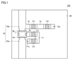
- FIG. 1 is a plan view of a circuit device according to Embodiment 1;
- FIG. 1 is a circuit diagram of a circuit device according to Embodiment 1;
- FIG. 1 is a perspective view of a coil component according to Embodiment 1;
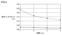
- FIG. 5 is a graph for explaining changes in parasitic inductance in the circuit device according to the first embodiment;
- FIG. 3 is a plan view of a circuit device according to a comparative example; 3 is a plan view of the circuit device according to the first embodiment when some capacitors are not mounted;
- FIG. 10 is a plan view of a circuit device according to a first modification of the first embodiment;
- FIG. 11 is a plan view of a circuit device according to a second modification of the first embodiment;
- FIG. 11 is a plan view of a circuit device according to a third modification of the first embodiment;
- FIG. 12 is a plan view of a circuit device according to a fourth modification of the first embodiment;
- FIG. 11 is a plan view of a circuit device according to a second embodiment;
- FIG. 11 is a plan view of a circuit device according to a first modification of the second embodiment;
- FIG. 11 is a plan view of a circuit device according to a second modification of the second embodiment;
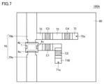
- FIG. 1 is a plan view of a circuit device 100 according to Embodiment 1.
- the circuit device 100 is, for example, a filter circuit used as a noise countermeasure for the power supply line 70, and is mounted with a coil component 1 including two coils magnetically coupled to cancel the parasitic inductance of the capacitors C1 and C2.
- the circuit device 100 is not limited to the filter circuit used for noise countermeasures on the power supply line 70, and may be a filter circuit used for noise countermeasures on other signal lines or the like.
- the circuit device 100 has a wiring pattern of the power supply line 70 formed on the surface of the substrate 60, and the coil component 1 is mounted in series with the power supply line 70.
- the power supply line 70 includes a first wiring 70 a connected to the input terminal 4 a of the coil component 1 and a second wiring 70 b connected to the output terminal 4 b of the coil component 1 .
- the substrate 60 is formed by laminating a plurality of insulating layers, and is formed of, for example, low-temperature co-fired ceramics, glass epoxy resin, or the like.
- Wiring patterns such as first wiring 70a and second wiring 70b, electrode patterns for mounting components such as coil component 1 and capacitors C1 to C4, and the like are formed on the surface of substrate 60.
- Cu, Ag, Al, and the like are formed on the surface of substrate 60, respectively. is formed of a metal material that is generally adopted as an electrode material for
- two capacitors C1 and C2 are connected in series to the intermediate terminal 4c of the coil component 1.
- a wiring pattern of a third wiring 71 is formed on the substrate 60 as a wiring for mounting the capacitors C1 and C2.
- the third wiring 71 electrically connects the intermediate terminal 4c between the two coils included in the coil component 1 and the ground electrode 71a by mounting the capacitors C1 and C2.
- two capacitors C3 and C4 are connected in series between the second wiring 70b near the coil component 1 and the ground electrode 72a.
- a wiring pattern of the fourth wiring 72 is formed on the substrate 60 as wiring for mounting the capacitors C3 and C4.
- the fourth wiring 72 electrically connects the second wiring 70b and the ground electrode 72a by mounting the capacitors C3 and C4. Note that the fourth wiring 72 may be provided on the first wiring 70a instead of on the second wiring 70b.
- the ground electrode is an electrode that is electrically connected to the ground potential, and is composed of, for example, a conductive via that is electrically connected to the ground potential arranged in the inner layer of the substrate 60 .
- the third wiring 71 and the fourth wiring 72 are wirings for electrically connecting the coil component, the first wiring 70a, the second wiring 70b, the ground electrode 71a, and the ground electrode 72a, including the capacitor. is shown as a collection of wiring groups.
- the fourth wiring 72 extends linearly from the second wiring 70b to the ground electrode 72a as shown in FIG. 1, and has a linear shape.
- the third wiring 71 has a U-shape extending from the intermediate terminal 4c to the ground electrode 71a by bending twice.
- the shape of the third wiring 71 U-shaped instead of the same linear shape as the shape of the fourth wiring 72, it is possible to suppress changes in the parasitic inductance of the capacitors C1 and C2 as will be described later. can.
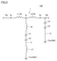
- FIG. 2 is a circuit diagram of the circuit device 100 according to the first embodiment.
- the circuit device 100 is specifically an EMI removal filter circuit, and is a third-order T-type LC filter circuit.
- a third-order T-type LC filter circuit is used as the configuration of the circuit device 100, but a fifth-order T-type LC filter circuit and a higher-order T-type LC filter circuit may be used.
- a similar configuration can be applied.
- the circuit device 100 includes a coil component 1 and capacitors C1 to C4.
- the coil component 1 includes an input terminal 4a, an output terminal 4b, an intermediate terminal 4c, a coil L1 (first coil), and a coil L2 (second coil).
- capacitors C1 and C2 are connected in series between the input terminal 4a and the ground electrode 71a as shown in FIG. Either one of the capacitors C1 and C2 may be used, but two capacitors are arranged in series to form a redundant circuit configuration, assuming that the capacitor is mounted on a vehicle. Similarly, capacitors C3 and C4 are connected in series between second wiring 70b and ground electrode 72a.
- Capacitors C1 to C4 are not only multilayer ceramic capacitors whose main component is BaTiO 3 (barium titanate), but also multilayer ceramic capacitors whose main component is other materials. other types of capacitors may be used.
- the capacitors C1 and C2 connected to the coil component 1 have an inductor L3 as a parasitic inductance (equivalent series inductance (ESL)). Therefore, the circuit device 100 is equivalent to a circuit configuration in which the inductor L3 is connected in series with the capacitors C1 and C2, as shown in FIG.
- a coil L1 and a coil L2 are connected to the intermediate terminal 4c in addition to the capacitors C1 and C2.
- the coils L1 and L2 are magnetically coupled to generate a negative inductance component (mutual inductance M).
- a negative inductance component (mutual inductance M)
- the parasitic inductance (inductor L3) of the capacitors C1 and C2 can be canceled, and the apparent inductance components of the capacitors C1 and C2 can be reduced.
- a mutual inductance M (-M) for canceling the inductor L3 is connected in series with the capacitors C1 and C2, and an equivalent It is shown as a circuit.
- the circuit device 100 composed of the capacitors C1 and C2, the coil L1 and the coil L2 cancels out the parasitic inductance of the capacitors C1 and C2 with a negative inductance component due to the mutual inductance M of the coil L1 and the coil L2, so that the high frequency band can improve the noise suppression effect of
- the coil component 1 is a transformer coil, and includes a coil L1 (first coil) and a coil L2 (second coil) provided in a laminate so that the coil surfaces face each other in the lamination direction. It is mounted parallel to the surface of 60.
- a configuration of the coil component 1 will be described with reference to the drawings.
- 3 is a perspective view of the coil component 1 according to Embodiment 1.
- the short side direction of the coil component 1 is the X direction
- the long side direction is the Y direction
- the height direction is the Z direction.
- the stacking direction of the substrates is the Z direction
- the direction of the arrow indicates the upper layer direction.
- the coil component 1 is composed of a ceramic layer laminate 3 (ceramic element body) in which a plurality of substrates (ceramic green sheets) on which coil wiring is formed are laminated.
- the laminate 3 has a pair of main surfaces facing each other and side surfaces connecting the main surfaces.
- a plurality of wiring patterns 10 forming the coil L1 and the coil L2 are stacked in parallel to the main surface of the laminate 3 from the bottom.
- the side surfaces of the laminate 3 are the first long side surface (the side surface on which the input terminal 4a (first external electrode) is formed) and the second side surface (the side surface on which the output terminal 4b (second external electrode) is formed). , and a third side surface (side surface on which the intermediate terminal 4c (third external electrode) is formed) and a fourth side surface (side surface on which the terminal 4d is formed) on the short side.
- a plurality of wiring patterns 10 forming the coils L1 and L2 are arranged inside the laminate 3.
- a part of the plurality of wiring patterns 10 forms the coil L1, and the rest forms the coil L2.
- the plurality of wiring patterns 10 have a common portion that constitutes the coils L1 and L2, so that fluctuations in magnetic coupling between the coils L1 and L2 can be reduced.
- the end portion 11 of the uppermost wiring pattern 10 is electrically connected to the input terminal 4a.
- the end portion 21 of the lowermost wiring pattern 10 among the plurality of wiring patterns 10 is electrically connected to the output terminal 4b.
- the end portion 31 of the middle-layer wiring pattern 10 is electrically connected to the intermediate terminal 4c.
- FIG. 4 is a graph for explaining changes in parasitic inductance in the circuit device 100 according to the first embodiment.
- the horizontal axis is the distance between wires
- the vertical axis is the amount of change in parasitic inductance.
- FIG. 5 is a plan view of a circuit device 300 according to a comparative example.
- circuit device 300 shown in FIG. 5 the same components as those of circuit device 100 shown in FIG. 1 are denoted by the same reference numerals, and detailed description thereof will not be repeated.
- the third wiring 71A for mounting the capacitors C1 and C2 is not U-shaped, but extends straight from the intermediate terminal 4c to the ground electrode 71a. and has a linear shape. Therefore, the third wiring 71A and the fourth wiring 72 are formed in parallel on the substrate 60 .
- the direction of the current flowing through the third wiring 71A and the direction of the current flowing through the fourth wiring 72 are always the same.
- the arrangement is such that the magnetic coupling between 71A and the fourth wiring 72 is strengthened. In the present disclosure, it is described that the two wirings are formed in parallel on the substrate. It doesn't have to be.
- the third wiring 71 for mounting the capacitors C1 and C2 is U-shaped, so the direction of the current flowing through the capacitor C1 and the direction of the current flowing through the capacitor C2 are different. Conversely, the magnetic coupling between the portion where the capacitor C1 is mounted and the portion where the capacitor C2 is mounted weaken each other.
- a path through which current flows from the coil component 1 to the ground electrode 71a through the third wiring 71 on which the capacitors C1 and C2 are mounted is called a first current path.
- the first current path includes a path through which current flows in the opposite direction.
- the magnetic coupling between the portion where the capacitor C1 is mounted and the portion where the capacitor C2 is mounted weakens each other, so that the magnetic coupling between the third wiring 71 and the fourth wiring 72 also weakens. That is, by making the third wiring 71 U-shaped, it is less likely to be affected by the magnetic coupling with the fourth wiring 72, and changes in the parasitic inductances of the capacitors C1 and C2 can be reduced.
- the shape of the third wiring 71 is a U-shape in which the capacitor C1 is mounted on one long side and the capacitor C2 is mounted on the other long side, but is not limited to this shape. , as long as it has a portion that is not parallel to the fourth wiring 72 .
- the third wiring 71 has a portion that is not parallel to the fourth wiring 72 , so that the influence of the magnetic coupling of the fourth wiring 72 to the third wiring 71 can be reduced.
- a path through which current flows from the second wiring 70b to the ground electrode 72a through the fourth wiring 72 having capacitors C3 and C4 mounted on the electrodes is referred to as a second current path.
- the fact that the third wiring 71 has a portion that is not parallel to the fourth wiring 72 means that the distance between the first current path and the second current path is not constant.
- the capacitor C1 and the capacitor C2 are mounted in parallel.
- the capacitors C1 and C2 can be mounted in the same direction, facilitating the mounting of the capacitors C1 and C2 on the substrate 60 .
- a first current path (path of the third wiring 71) leading to the coil component 1 and a second current path (path of the fourth wiring 72) leading to the second wiring 70b are arranged in parallel.
- the first current path (the path of the third wiring 71) is bent at a right angle from the middle. It should be noted that the angle at which the route bends may not be a right angle.
- the strength of the magnetic coupling between the third wiring and the fourth wiring also depends on the distance between the wirings.
- the amount of change in the parasitic inductance of the capacitors C1 and C2 due to the distance (shortest distance) between the U-shaped third wiring 71 and the U-shaped fourth wiring 72 in the circuit device 100 is represented by a solid line.
- the amounts of change in the parasitic inductances of the capacitors C1 and C2 due to the distance between the linear third wiring 71A and the straight fourth wiring 72 are indicated by dashed lines.
- the parasitic inductance of the capacitors C1 and C2 is increased compared to the configuration of the circuit device without the fourth wiring 72. It is increased by about 0.23 nH. Also, even when the distance between the third wiring 71A and the fourth wiring 72 is about 4 mm, the parasitic inductance of the capacitors C1 and C2 is increased by about 0.11 nH.
- the distance between the U-shaped third wiring 71 and the fourth wiring 72 in the circuit device 100 is short, for example, about 1 mm
- the distance between the capacitors C1 and C2 is smaller than that of the circuit device without the fourth wiring 72.
- the parasitic inductance changes only about 0.03nH.
- the parasitic inductance of the capacitors C1 and C2 changes only by approximately 0.02 nH.
- the wiring width of the third wiring 71 or the fourth wiring 72 is about 1 mm, and the shortest distance between the third wiring 71 and the fourth wiring 72 is about 4 mm or less (wiring width 4 times or less), the influence of the magnetic coupling of the fourth wiring 72 to the third wiring 71 is reduced.
- the change in parasitic inductance is small regardless of the distance between the surrounding wirings, and it can be said that the amount of parasitic inductance is small compared to the case where there is no wiring, so the change is small.
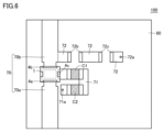
- FIG. 6 is a plan view of the circuit device 100 according to the first embodiment when some capacitors are not mounted.
- the circuit device 100 includes the substrate 60 on which the wiring pattern is formed, and the coil component 1 mounted on the substrate 60 .
- the coil component 1 includes a coil L1 and a coil L2, the coil L1 and the coil L2 are magnetically coupled, the first end of the coil L1 is connected to the input terminal 4a, and the second end of the coil L2 and the coil L2 are connected. is connected to the intermediate terminal 4c, and the second end of the coil L2 is connected to the output terminal 4b.
- a first wiring 70a connected to the input terminal 4a of the coil component 1 a second wiring 70b connected to the output terminal 4b of the coil component 1, and capacitors C1 and C2 are mounted in series.
- a third wiring 71 connecting the intermediate terminal 4c between the coil L2 and the ground electrode 71a, and an electrode for mounting the capacitors C3 and C4 in series are provided. and a fourth wiring 72 that connects with the electrode 72a.
- the third wiring 71 and the fourth wiring 72 have portions that are not parallel.
- the circuit device 100 has a portion where the third wiring 71 and the fourth wiring 72 are not parallel. A change in parasitic inductance of the capacitors C1 and C2 can be suppressed.
- capacitors are mounted on each of the third wiring 71 and the fourth wiring 72 . This makes it possible to realize a redundant circuit configuration that does not short-circuit even if one capacitor fails.
- the shortest distance between the third wiring 71 and the fourth wiring 72 is preferably four times or less the wiring width of the third wiring 71 or the fourth wiring 72 .
- the circuit device 100 has a portion where the third wiring 71 and the fourth wiring 72 are not parallel, so that the influence of the magnetic coupling of the fourth wiring 72 to the third wiring 71 can be effectively weakened.
- the shape of the third wiring 71 or the fourth wiring 72 is preferably U-shaped. Thereby, the influence of the magnetic coupling of the fourth wiring 72 with respect to the third wiring 71 can be further weakened. Furthermore, the portion where the capacitor is mounted can be made compact.
- the capacitors When two or more capacitors are mounted on the U-shaped third wiring 71, it is preferable to mount the capacitors at positions where the capacitors are parallel to each other. This allows the capacitors to be mounted in the same direction, facilitating the mounting of the capacitors on the substrate 60 .
- FIG. 7 is a plan view of a circuit device 100A according to the first modification of the first embodiment.
- circuit device 100A shown in FIG. 7 the same components as those of circuit device 100 shown in FIG. 1 are denoted by the same reference numerals, and detailed description thereof will not be repeated.
- the third wiring 71B for mounting the capacitors C1 and C2 is not U-shaped, but L-shaped from the intermediate terminal 4c to the ground electrode 71a. Since the L-shaped third wiring 71B has a shape that has a portion that is not parallel to the fourth wiring 72, the influence of the magnetic coupling of the fourth wiring 72 to the third wiring 71B can be reduced.
- the L-shaped third wiring 71B includes a capacitor C1 (first capacitor) among the mounted capacitors that is closer to the coil component 1, and a capacitor C3 that is among the capacitors mounted on the fourth wiring 72 and is closer to the coil component 1. (The second capacitor) is preferably parallel to the mounting direction.
- FIG. 8 is a plan view of a circuit device 100B according to a second modification of the first embodiment.
- circuit device 100B shown in FIG. 8 the same components as those of circuit device 100 shown in FIG. 1 are denoted by the same reference numerals, and detailed description thereof will not be repeated.
- a wiring pattern of the fifth wiring 73 is formed on the substrate 60 as wiring for mounting the capacitors C5 and C6.
- the fifth wiring 73 electrically connects the first wiring 70a and the ground electrode 73a by mounting the capacitors C5 and C6.
- the fifth wiring 73 extends linearly from the first wiring 70a to the ground electrode 73a and has a linear shape.
- the fifth wiring 73 exerts a magnetic coupling effect on the adjacent third wiring 71, but the U-shaped third wiring 71 alleviates the influence.
- the wiring pattern is provided with electrodes for mounting the capacitors C5 and C6, and includes a fifth wiring 73 connecting a first wiring 70a or a second wiring 70b different from the wiring to which the fourth wiring 72 is connected and the ground electrode 73a. Further, it is preferable that the third wiring 71 and the fifth wiring 73 have a portion where they are not parallel.
- the circuit device 100B has a portion where the third wiring 71 and the fifth wiring 73 are not parallel, the influence of the magnetic coupling of the fifth wiring 73 on the third wiring 71 is weakened, and the parasitics of the capacitors C1 and C2 are reduced. A change in inductance can be suppressed.
- At least one or more capacitors are mounted on the electrodes provided on the fifth wiring 73 .
- Mounting a capacitor on the fifth wiring 73 causes magnetic coupling between the third wiring 71 and the fifth wiring 73. Therefore, in the circuit device 100B, the third wiring 71 and the fifth wiring 73 are not parallel. By having the portion, the influence of the magnetic coupling of the fifth wiring 73 to the third wiring 71 can be effectively weakened.
- capacitors are mounted on each of the third wiring 71 and the fifth wiring 73 . This makes it possible to realize a redundant circuit configuration that does not short-circuit even if one capacitor fails.
- the circuit device 100B may be provided with a plurality of fourth wirings and a plurality of fifth wirings as shown in FIG.
- the plurality of fourth wirings include, in addition to the fourth wirings 72, fourth wirings 74 for mounting the capacitors C7 and C8, and fourth wirings 75 for mounting the capacitors C9 and C10.
- the fourth wiring 74 electrically connects the second wiring 70b and the ground electrode 74a by mounting the capacitors C7 and C8.
- the fourth wiring 75 electrically connects the second wiring 70b and the ground electrode 75a by mounting the capacitors C9 and C10.
- the plurality of fifth wirings includes, in addition to the fifth wirings 73, fifth wirings 76 for mounting the capacitors C11 and C12.
- the fifth wiring 76 electrically connects the first wiring 70a and the ground electrode 76a by mounting the capacitors C11 and C12.
- a current flows from the second wiring 70b to the ground electrode 74a through a fourth wiring 74 having capacitors C7 and C8 mounted on the electrodes, and a fourth wiring 75 having capacitors C9 and C10 mounted on the electrodes from the second wiring 70b.
- the path through which the current flows to the ground electrode 75a is also an example of the second current path.
- a current flows from the first wiring 70a to the ground electrode 73a through a fifth wiring 73 having capacitors C5 and C6 mounted on the electrodes, and a fifth wiring 76 having capacitors C11 and C12 mounted on the electrodes from the first wiring 70a.
- a path through which current flows to the ground electrode 76a is an example of a third current path.
- the path of the fourth wirings 72, 74, 75 electrically connected to the second wiring 70b is called the third current path
- the path of the fifth wirings 73, 76 electrically connected to the first wiring 70a is called the third current path. It may be called a two-current path.
- FIG. 9 is a plan view of circuit devices 100C1 and 100C2 according to the third modification of the first embodiment.
- circuit devices 100C1 and 100C2 shown in FIG. 9 the same configurations as those of circuit device 100 shown in FIG. 1 are denoted by the same reference numerals, and detailed description thereof will not be repeated.
- the fourth wiring 72A for mounting the capacitors C3 and C4 does not have a linear shape, but has a U-shape extending from the second wiring 70b to the ground electrode 72a. . Both the shape of the third wiring 71 and the shape of the fourth wiring 72A are U-shaped. Thereby, the circuit device 100C1 can further weaken the influence of the magnetic coupling of the fourth wiring 72A to the third wiring 71.
- FIG. 9A the fourth wiring 72A for mounting the capacitors C3 and C4 does not have a linear shape, but has a U-shape extending from the second wiring 70b to the ground electrode 72a. .
- Both the shape of the third wiring 71 and the shape of the fourth wiring 72A are U-shaped. Thereby, the circuit device 100C1 can further weaken the influence of the magnetic coupling of the fourth wiring 72A to the third wiring 71.
- the bending direction of the third wiring 71 and the bending direction of the fourth wiring 72A are the same. That is, the first current path (the path of the third wiring 71) and the second current path (the path of the fourth wiring 72A) have the same shape, and each path has at least one bending point. Therefore, the direction of the current flowing in the capacitor C1 portion of the third wiring 71 and the capacitor C4 portion of the fourth wiring 72A is reversed. That is, in the circuit device 100C1, the directions of the currents flowing through the adjacent wirings are opposite to each other, so that the parasitic inductances of the capacitors C1 and C2 can be further reduced.
- the fourth wiring 72A1 for mounting the capacitors C3 and C4 does not have a linear shape, but has a U-shape extending from the second wiring 70b to the ground electrode 72a.
- Both the shape of the third wiring 71 and the shape of the fourth wiring 72A1 are U-shaped. Thereby, the circuit device 100C2 can further weaken the influence of the magnetic coupling of the fourth wiring 72A1 to the third wiring 71.
- the bending direction of the third wiring 71 and the bending direction of the fourth wiring 72A1 are different directions. That is, the distance between the first current path (the path of the third wiring 71) and the second current path (the path of the fourth wiring 72A1) is not constant, and both are U-shaped.
- the shape of the fifth wiring may also be U-shaped. Thereby, the circuit devices 100C1 and 100C2 can further weaken the influence of the magnetic coupling of the fifth wiring to the third wiring 71.
- FIG. 1 A block diagram illustrating an exemplary computing environment in accordance with the present disclosure.
- FIG. 10 is a plan view of circuit devices 100D1 and D2 according to the fourth modification of the first embodiment.
- circuit devices 100D1 and D2 shown in FIG. 10 the same configurations as those of circuit device 100 shown in FIG. 7 are denoted by the same reference numerals, and detailed description thereof will not be repeated.
- one capacitor C1 is mounted on the L-shaped third wiring 71B, and one capacitor C3 is mounted on the linear fourth wiring 72.
- two capacitors C1 and C2 may be mounted on the L-shaped third wiring 71B, and one capacitor C3 may be mounted on the linear fourth wiring 72.
- one capacitor C1 may be mounted on the L-shaped third wiring 71B, and two capacitors C3 and C4 may be mounted on the linear fourth wiring 72.
- one capacitor C1 is mounted on the L-shaped third wiring 71B, and one capacitor C3 is mounted on the L-shaped fourth wiring 72B in the same direction.
- two capacitors C1 and C2 are mounted on the L-shaped third wiring 71B, and one capacitor C3 is mounted on the L-shaped fourth wiring 72B in the same direction.
- one capacitor C1 may be mounted on the L-shaped third wiring 71B, and two capacitors C3 and C4 may be mounted on the L-shaped fourth wiring 72B in the same direction.
- the L-shaped third wiring 71B and the L-shaped fourth wiring 72B may be oriented in different directions.
- the shape of the fifth wiring may also be L-shaped. Thereby, the circuit devices 100D1 and 100D2 can further weaken the influence of the magnetic coupling of the fifth wiring with respect to the third wiring 71.
- FIG. 1 A block diagram illustrating an exemplary computing environment in accordance with the present disclosure.
- FIG. 11 is a plan view of the circuit device 200 according to the second embodiment.
- the same components as those of circuit device 100 shown in FIG. 1 are denoted by the same reference numerals, and detailed description thereof will not be repeated.
- the circuit device 200 has a wiring pattern of the power supply line 70 formed on the surface of the substrate 60 and the coil component 1 is mounted in series with the power supply line 70 .
- the power supply line 70 includes a first wiring 70 a connected to the input terminal 4 a of the coil component 1 and a second wiring 70 b connected to the output terminal 4 b of the coil component 1 .
- a wiring pattern of the third wiring 71A is formed on the substrate 60 as wiring for mounting the capacitors C1 and C2.
- the third wiring 71A electrically connects the intermediate terminal 4c between the two coils included in the coil component 1 and the ground electrode 71a by mounting the capacitors C1 and C2.
- two capacitors C3 and C4 are connected in series to the second wiring 70b in the vicinity of the coil component 1.
- a wiring pattern of the fourth wiring 72A is formed on the substrate 60 as wiring for mounting the capacitors C3 and C4.
- the fourth wiring 72A electrically connects the second wiring 70b and the ground electrode 72a by mounting the capacitors C3 and C4.
- the fourth wiring 72A may be provided on the first wiring 70a instead of on the second wiring 70b.
- the third wiring 71A extends linearly from the intermediate terminal 4c to the ground electrode 71a and has a linear shape.
- the fourth wiring 72A is U-shaped from the second wiring 70b to the ground electrode 72a by bending twice.
- the shape of the fourth wiring 72A U-shaped instead of the same linear shape as the shape of the third wiring 71A, the influence of the magnetic coupling of the fourth wiring 72A to the third wiring 71A is reduced. Therefore, changes in the parasitic inductance of the capacitors C1 and C2 can be suppressed.
- the shape of the third wiring 71A is linear, whereas the shape of the fourth wiring 72A is U-shaped. 71A and 72 A of 4th wiring will have a part which is not parallel.
- the circuit device 200 according to the second embodiment has a portion where the third wiring 71A and the fourth wiring 72A are not parallel. A change in parasitic inductance of the capacitors C1 and C2 can be suppressed.
- At least one or more capacitors are mounted on the electrodes provided on the fourth wiring 72A. Moreover, it is preferable that two or more capacitors are mounted on each of the third wiring 71A and the fourth wiring 72A.
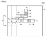
- FIG. 12 is a plan view of a circuit device 200A according to the first modification of the second embodiment.
- circuit device 200A shown in FIG. 12 the same configurations as circuit device 200 shown in FIG. 11 are denoted by the same reference numerals, and detailed description thereof will not be repeated.
- the fourth wiring 72B for mounting the capacitors C3 and C4 is not U-shaped, but L-shaped from the second wiring 70b to the ground electrode 72a. Since the L-shaped fourth wiring 72B has a shape that has a portion that is not parallel to the third wiring 71A, the influence of the magnetic coupling of the fourth wiring 72B to the third wiring 71A can be reduced.
- the mounting directions of the capacitor C3 near the coil component 1 among the mounted capacitors and the capacitor C1 near the coil component 1 among the capacitors mounted on the third wiring 71A are different. Parallelism is preferred.
- the influence of the magnetic coupling of the fourth wiring 72B on the third wiring 71A can be effectively weakened.
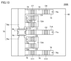
- FIG. 13 is a plan view of a circuit device 200B according to a second modification of the second embodiment.
- circuit device 200B shown in FIG. 13 the same configurations as those of circuit device 200 shown in FIG. 11 are denoted by the same reference numerals, and detailed description thereof will not be repeated.
- a wiring pattern of the fifth wiring 73A is formed on the substrate 60 as wiring for mounting the capacitors C5 and C6.
- the fifth wiring 73A electrically connects the first wiring 70a and the ground electrode 73a by mounting the capacitors C5 and C6.
- the fifth wiring 73A has a U-shape extending from the first wiring 70a to the ground electrode 73a by bending twice.
- the fifth wiring 73A exerts a magnetic coupling effect on the adjacent third wiring 71A, but the U-shape can alleviate the influence.
- the wiring pattern is provided with electrodes for mounting the capacitors C5 and C6, and includes a fifth wiring 73A connecting the first wiring 70a or the second wiring 70b different from the wiring to which the fourth wiring 72A is connected and the ground electrode 73a. Further, it is preferable that the third wiring 71A and the fifth wiring 73A have a portion where they are not parallel.
- the fourth wiring 72A and the fifth wiring 73A are bent in the same direction in FIG. 13, they do not necessarily have to be in the same direction. may
- the circuit device 200B has a portion where the third wiring 71A and the fifth wiring 73A are not parallel, the influence of the magnetic coupling of the fifth wiring 73A on the third wiring 71A is weakened, and the parasitics of the capacitors C1 and C2 are reduced. A change in inductance can be suppressed.
- At least one capacitor is mounted on the electrode provided on the fifth wiring 73A. Mounting a capacitor on the fifth wiring 73A causes magnetic coupling between the third wiring 71A and the fifth wiring 73A. By having the portion, the influence of the magnetic coupling of the fifth wiring 73A to the third wiring 71A can be effectively weakened.
- capacitors are mounted on each of the third wiring 71A and the fifth wiring 73A. This makes it possible to realize a redundant circuit configuration that does not short-circuit even if one capacitor fails.
- the circuit device 200B may be provided with a plurality of fourth wirings and a plurality of fifth wirings as shown in FIG.
- the plurality of fourth wirings includes fourth wirings 74 for mounting the capacitors C7 and C8 in addition to the fourth wirings 72A.
- the fourth wiring 74 electrically connects the second wiring 70b and the ground electrode 74a by mounting the capacitors C7 and C8.
- the plurality of fifth wirings includes fifth wirings 76 for mounting the capacitors C11 and C12 in addition to the fifth wirings 73A.
- the fifth wiring 76 electrically connects the first wiring 70a and the ground electrode 76a by mounting the capacitors C11 and C12.
- the fifth wiring 73A is described as being U-shaped in FIG. 13, it is not limited to this, and may be L-shaped, for example.
- the first current path (the path of the third wiring 71) should be bent in the middle (the U-shaped third wiring 71).
- the wiring 71, L-shaped third wiring 71B) is preferable.
Landscapes
- Engineering & Computer Science (AREA)
- Power Engineering (AREA)
- Microelectronics & Electronic Packaging (AREA)
- Manufacturing & Machinery (AREA)
- Filters And Equalizers (AREA)
Priority Applications (3)
| Application Number | Priority Date | Filing Date | Title |
|---|---|---|---|
| JP2023561532A JP7626247B2 (ja) | 2021-11-22 | 2022-11-07 | 回路装置 |
| CN202280076452.0A CN118302957A (zh) | 2021-11-22 | 2022-11-07 | 电路装置 |
| US18/663,139 US20240297631A1 (en) | 2021-11-22 | 2024-05-14 | Circuit device |
Applications Claiming Priority (2)
| Application Number | Priority Date | Filing Date | Title |
|---|---|---|---|
| JP2021189637 | 2021-11-22 | ||
| JP2021-189637 | 2021-11-22 |
Related Child Applications (1)
| Application Number | Title | Priority Date | Filing Date |
|---|---|---|---|
| US18/663,139 Continuation US20240297631A1 (en) | 2021-11-22 | 2024-05-14 | Circuit device |
Publications (1)
| Publication Number | Publication Date |
|---|---|
| WO2023090181A1 true WO2023090181A1 (ja) | 2023-05-25 |
Family
ID=86396908
Family Applications (1)
| Application Number | Title | Priority Date | Filing Date |
|---|---|---|---|
| PCT/JP2022/041328 Ceased WO2023090181A1 (ja) | 2021-11-22 | 2022-11-07 | 回路装置 |
Country Status (4)
| Country | Link |
|---|---|
| US (1) | US20240297631A1 (https=) |
| JP (1) | JP7626247B2 (https=) |
| CN (1) | CN118302957A (https=) |
| WO (1) | WO2023090181A1 (https=) |
Cited By (1)
| Publication number | Priority date | Publication date | Assignee | Title |
|---|---|---|---|---|
| WO2024166971A1 (ja) * | 2023-02-09 | 2024-08-15 | 株式会社村田製作所 | 回路装置、および回路基板 |
Citations (3)
| Publication number | Priority date | Publication date | Assignee | Title |
|---|---|---|---|---|
| JPH0310403A (ja) * | 1989-06-07 | 1991-01-18 | Sharp Corp | マイクロ波回路 |
| JP2005294975A (ja) * | 2004-03-31 | 2005-10-20 | Densei Lambda Kk | ノイズフィルタ |
| WO2021085002A1 (ja) * | 2019-10-30 | 2021-05-06 | 株式会社村田製作所 | コイル部品および、これを含むフィルタ回路 |
Family Cites Families (1)
| Publication number | Priority date | Publication date | Assignee | Title |
|---|---|---|---|---|
| CN107408931B (zh) * | 2015-07-28 | 2020-06-19 | 株式会社村田制作所 | 电路基板、使用其的滤波器电路以及电容器元件 |
-
2022
- 2022-11-07 WO PCT/JP2022/041328 patent/WO2023090181A1/ja not_active Ceased
- 2022-11-07 JP JP2023561532A patent/JP7626247B2/ja active Active
- 2022-11-07 CN CN202280076452.0A patent/CN118302957A/zh active Pending
-
2024
- 2024-05-14 US US18/663,139 patent/US20240297631A1/en active Pending
Patent Citations (3)
| Publication number | Priority date | Publication date | Assignee | Title |
|---|---|---|---|---|
| JPH0310403A (ja) * | 1989-06-07 | 1991-01-18 | Sharp Corp | マイクロ波回路 |
| JP2005294975A (ja) * | 2004-03-31 | 2005-10-20 | Densei Lambda Kk | ノイズフィルタ |
| WO2021085002A1 (ja) * | 2019-10-30 | 2021-05-06 | 株式会社村田製作所 | コイル部品および、これを含むフィルタ回路 |
Cited By (1)
| Publication number | Priority date | Publication date | Assignee | Title |
|---|---|---|---|---|
| WO2024166971A1 (ja) * | 2023-02-09 | 2024-08-15 | 株式会社村田製作所 | 回路装置、および回路基板 |
Also Published As
| Publication number | Publication date |
|---|---|
| CN118302957A (zh) | 2024-07-05 |
| US20240297631A1 (en) | 2024-09-05 |
| JP7626247B2 (ja) | 2025-02-04 |
| JPWO2023090181A1 (https=) | 2023-05-25 |
Similar Documents
| Publication | Publication Date | Title |
|---|---|---|
| CN216162684U (zh) | 线圈部件及包含该线圈部件的滤波器电路 | |
| JP7107463B1 (ja) | 電子機器 | |
| CN219164535U (zh) | 滤波器电路以及包含该滤波器电路的电源装置 | |
| US11870412B2 (en) | Multilayer substrate, circuit device, and filter circuit substrate | |
| JP5870674B2 (ja) | 積層コンデンサアレイ | |
| US11264162B2 (en) | Coil component and filter circuit including the coil component | |
| US10284164B2 (en) | Circuit substrate, filter circuit, and capacitance element | |
| WO2023090181A1 (ja) | 回路装置 | |
| WO2017017987A1 (ja) | 回路基板、これを用いたフィルタ回路およびキャパシタンス素子 | |
| US12040768B2 (en) | Circuit device and filter circuit | |
| WO2023210499A1 (ja) | 回路装置、およびフィルタ回路 | |
| CN223427310U (zh) | 线圈部件和包含该线圈部件的滤波电路 | |
| CN222980246U (zh) | 线圈部件和包含该线圈部件的滤波电路 | |
| JP2025172409A (ja) | コイル部品および、これを含むフィルタ回路 | |
| WO2022137678A1 (ja) | コイル部品および、これを含むフィルタ回路 | |
| WO2023210281A1 (ja) | コイル部品、およびフィルタ回路 | |
| WO2026048259A1 (ja) | コイル部品、これを含む電子機器 | |
| WO2024154387A1 (ja) | コイル部品、これを含むフィルタ回路 |
Legal Events
| Date | Code | Title | Description |
|---|---|---|---|
| 121 | Ep: the epo has been informed by wipo that ep was designated in this application |
Ref document number: 22895463 Country of ref document: EP Kind code of ref document: A1 |
|
| ENP | Entry into the national phase |
Ref document number: 2023561532 Country of ref document: JP Kind code of ref document: A |
|
| WWE | Wipo information: entry into national phase |
Ref document number: 202280076452.0 Country of ref document: CN |
|
| NENP | Non-entry into the national phase |
Ref country code: DE |
|
| 122 | Ep: pct application non-entry in european phase |
Ref document number: 22895463 Country of ref document: EP Kind code of ref document: A1 |