WO2023090141A1 - 電解コンデンサ素子 - Google Patents
電解コンデンサ素子 Download PDFInfo
- Publication number
- WO2023090141A1 WO2023090141A1 PCT/JP2022/040754 JP2022040754W WO2023090141A1 WO 2023090141 A1 WO2023090141 A1 WO 2023090141A1 JP 2022040754 W JP2022040754 W JP 2022040754W WO 2023090141 A1 WO2023090141 A1 WO 2023090141A1
- Authority
- WO
- WIPO (PCT)
- Prior art keywords
- layer
- electrolytic capacitor
- conductive polymer
- capacitor element
- solid electrolyte
- Prior art date
- Legal status (The legal status is an assumption and is not a legal conclusion. Google has not performed a legal analysis and makes no representation as to the accuracy of the status listed.)
- Ceased
Links
Images


Classifications
-
- H—ELECTRICITY
- H01—ELECTRIC ELEMENTS
- H01G—CAPACITORS; CAPACITORS, RECTIFIERS, DETECTORS, SWITCHING DEVICES, LIGHT-SENSITIVE OR TEMPERATURE-SENSITIVE DEVICES OF THE ELECTROLYTIC TYPE
- H01G9/00—Electrolytic capacitors, rectifiers, detectors, switching devices, light-sensitive or temperature-sensitive devices; Processes of their manufacture
- H01G9/004—Details
- H01G9/04—Electrodes or formation of dielectric layers thereon
- H01G9/042—Electrodes or formation of dielectric layers thereon characterised by the material
-
- H—ELECTRICITY
- H01—ELECTRIC ELEMENTS
- H01G—CAPACITORS; CAPACITORS, RECTIFIERS, DETECTORS, SWITCHING DEVICES, LIGHT-SENSITIVE OR TEMPERATURE-SENSITIVE DEVICES OF THE ELECTROLYTIC TYPE
- H01G11/00—Hybrid capacitors, i.e. capacitors having different positive and negative electrodes; Electric double-layer [EDL] capacitors; Processes for the manufacture thereof or of parts thereof
- H01G11/22—Electrodes
- H01G11/30—Electrodes characterised by their material
- H01G11/48—Conductive polymers
-
- H—ELECTRICITY
- H01—ELECTRIC ELEMENTS
- H01G—CAPACITORS; CAPACITORS, RECTIFIERS, DETECTORS, SWITCHING DEVICES, LIGHT-SENSITIVE OR TEMPERATURE-SENSITIVE DEVICES OF THE ELECTROLYTIC TYPE
- H01G9/00—Electrolytic capacitors, rectifiers, detectors, switching devices, light-sensitive or temperature-sensitive devices; Processes of their manufacture
- H01G9/0029—Processes of manufacture
- H01G9/0036—Formation of the solid electrolyte layer
-
- H—ELECTRICITY
- H01—ELECTRIC ELEMENTS
- H01G—CAPACITORS; CAPACITORS, RECTIFIERS, DETECTORS, SWITCHING DEVICES, LIGHT-SENSITIVE OR TEMPERATURE-SENSITIVE DEVICES OF THE ELECTROLYTIC TYPE
- H01G9/00—Electrolytic capacitors, rectifiers, detectors, switching devices, light-sensitive or temperature-sensitive devices; Processes of their manufacture
- H01G9/004—Details
- H01G9/02—Diaphragms; Separators
-
- H—ELECTRICITY
- H01—ELECTRIC ELEMENTS
- H01G—CAPACITORS; CAPACITORS, RECTIFIERS, DETECTORS, SWITCHING DEVICES, LIGHT-SENSITIVE OR TEMPERATURE-SENSITIVE DEVICES OF THE ELECTROLYTIC TYPE
- H01G9/00—Electrolytic capacitors, rectifiers, detectors, switching devices, light-sensitive or temperature-sensitive devices; Processes of their manufacture
- H01G9/004—Details
- H01G9/022—Electrolytes; Absorbents
- H01G9/025—Solid electrolytes
- H01G9/028—Organic semiconducting electrolytes, e.g. TCNQ
-
- H—ELECTRICITY
- H01—ELECTRIC ELEMENTS
- H01G—CAPACITORS; CAPACITORS, RECTIFIERS, DETECTORS, SWITCHING DEVICES, LIGHT-SENSITIVE OR TEMPERATURE-SENSITIVE DEVICES OF THE ELECTROLYTIC TYPE
- H01G9/00—Electrolytic capacitors, rectifiers, detectors, switching devices, light-sensitive or temperature-sensitive devices; Processes of their manufacture
- H01G9/15—Solid electrolytic capacitors
-
- H—ELECTRICITY
- H01—ELECTRIC ELEMENTS
- H01G—CAPACITORS; CAPACITORS, RECTIFIERS, DETECTORS, SWITCHING DEVICES, LIGHT-SENSITIVE OR TEMPERATURE-SENSITIVE DEVICES OF THE ELECTROLYTIC TYPE
- H01G9/00—Electrolytic capacitors, rectifiers, detectors, switching devices, light-sensitive or temperature-sensitive devices; Processes of their manufacture
- H01G9/004—Details
- H01G9/04—Electrodes or formation of dielectric layers thereon
- H01G9/048—Electrodes or formation of dielectric layers thereon characterised by their structure
- H01G9/055—Etched foil electrodes
Definitions
- the present invention relates to electrolytic capacitor elements.
- Patent Document 1 discloses a first oxide dielectric layer formed on the surface of the anode body, a second oxide dielectric layer formed on the exposed end face by cutting the anode body, and a first oxide dielectric layer.
- a solid electrolytic capacitor is disclosed having a first conductive polymer layer formed on a body layer and a second conductive polymer layer formed on a second oxide dielectric layer, It is described that the second conductive polymer layer is easier to insulate than the first conductive polymer layer.
- Patent Document 1 by covering a second oxide dielectric layer having a low withstand voltage formed on a cut surface of an anode body with a second conductive polymer layer, the second conductive polymer layer is insulated. Therefore, it is possible to provide a solid electrolytic capacitor with a low leakage current defect rate without a decrease in capacitance.
- the mechanism of insulation is not clear, and the measure for making the second conductive polymer layer easy to insulate is the addition of an insulating binder.
- ESR equivalent series resistance
- leakage current is not sufficiently reduced because locations where an electric field tends to concentrate when voltage is applied, such as corners, are not covered with the second conductive polymer layer.
- the present invention has been made to solve the above problems, and an object of the present invention is to provide an electrolytic capacitor element capable of suppressing leakage current while suppressing an increase in equivalent series resistance.
- An electrolytic capacitor element of the present invention comprises a valve-acting metal substrate, an anode having a distal end surface and a proximal end surface, and a dielectric layer provided on at least one main surface of the anode except at least the proximal end surface.
- a mask layer made of an insulating material and provided on the dielectric layer along the base end face; and a cathode provided on the dielectric layer on the tip face side of the mask layer.
- the cathode has a solid electrolyte layer provided on the dielectric layer, and a conductive layer provided on the solid electrolyte layer, the solid electrolyte layer being doped with a first dopant
- the first layer is partially arranged in the plane of the solid electrolyte layer, the first layer is arranged at least in a region where the second layer is not arranged in the plane of the solid electrolyte layer, and the second conductive polymer dedoping occurs more easily than the first conductive polymer.
- an electrolytic capacitor element capable of suppressing leakage current while suppressing an increase in equivalent series resistance.
- FIG. 1 is a plan view schematically showing an example of an electrolytic capacitor element according to an embodiment of the invention.
- FIG. 2 is a cross-sectional view of the electrolytic capacitor element shown in FIG. 1 along line XX.
- 3 is a perspective view of the electrolytic capacitor element shown in FIG. 1.
- FIG. 4 is a cross-sectional view of the electrolytic capacitor element shown in FIG. 3 along line AA.
- FIG. 5 is a cross-sectional view of the electrolytic capacitor element shown in FIG. 3 along line BB.
- FIG. 6 is a perspective view schematically showing an example of an electrolytic capacitor element according to another embodiment of the invention. 7 is a cross-sectional view of the electrolytic capacitor element shown in FIG. 6 along line CC.
- FIG. 8 is a cross-sectional view of the electrolytic capacitor element shown in FIG. 6 taken along line DD.
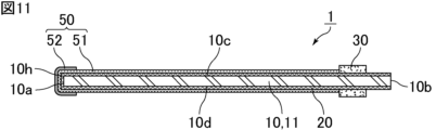
- FIG. 9 is a perspective view schematically showing an example of an electrolytic capacitor element according to still another embodiment of the invention.
- 10 is a cross-sectional view of the electrolytic capacitor element shown in FIG. 9 taken along line EE.
- 11 is a cross-sectional view of the electrolytic capacitor element shown in FIG. 9 taken along line FF.
- FIG. 12 is a perspective view schematically showing an example of an electrolytic capacitor element according to still another embodiment of the invention.
- 13 is a cross-sectional view of the electrolytic capacitor element shown in FIG. 12 along line GG.
- 14 is a cross-sectional view of the electrolytic capacitor element shown in FIG. 12 taken along line HH.
- FIG. 15 is an enlarged cross-sectional view of the mask layer portion of the electrolytic capacitor element shown in FIG. 2.
- FIG. FIG. 16 is a schematic diagram showing an example of a process of preparing a valve metal substrate on which a mask layer is formed.
- FIG. 17 is a schematic diagram showing an example of the process of forming the first layer of the solid electrolyte layer.
- FIG. 18 is a schematic diagram showing an example of the process of forming the second layer of the solid electrolyte layer.
- FIG. 19 is a perspective view schematically showing an example of an electrolytic capacitor including an electrolytic capacitor element according to an embodiment of the invention. 20 is a cross-sectional view of the electrolytic capacitor shown in FIG. 19 taken along line ZZ.
- the electrolytic capacitor element of the present invention will be described below.
- the present invention is not limited to the following configurations, and can be appropriately modified and applied without changing the gist of the present invention. Combinations of two or more of the individual desirable configurations described below are also part of the present invention.
- FIG. 1 is a plan view schematically showing an example of an electrolytic capacitor element according to an embodiment of the invention.
- FIG. 2 is a cross-sectional view of the electrolytic capacitor element shown in FIG. 1 along line XX. Note that in FIG. 1, the solid electrolyte layer 50 covered with the conductive layer 60 is indicated by a dashed line. 1 and 2 show the solid electrolyte layer 50 without distinguishing the first layer 51 and the second layer 52 from each other.
- the electrolytic capacitor element 1 shown in FIGS. 1 and 2 is a solid electrolytic capacitor element, which is composed of a valve action metal substrate 11, an anode 10 having a distal end surface 10a and a proximal end surface 10b, and an anode 10 except for the proximal end surface 10b.
- FIG. 3 is a perspective view of the electrolytic capacitor element shown in FIG. 4 is a cross-sectional view of the electrolytic capacitor element shown in FIG. 3 along line AA.
- FIG. 5 is a cross-sectional view of the electrolytic capacitor element shown in FIG. 3 along line BB.
- 3 4 and 5 show the state before the conductive layer 60 of the cathode 40 is formed. 3, the illustration of the dielectric layer 20 is omitted, and the first layer 51 of the solid electrolyte layer 50 is indicated by a dashed line, showing the first layer 51 as seen through.
- the solid electrolyte layer 50 includes a first layer 51 including a first conductive polymer doped with a first dopant and a first layer 51 including a first conductive polymer doped with a second dopant. and a second layer 52 containing a second conductive polymer, the second layer 52 being partially arranged in the plane of the solid electrolyte layer 50, and the first layer 51 being the solid electrolyte It is arranged at least in a region where the second layer 52 is not arranged in the plane of the layer 50 .
- the second conductive polymer is more likely to be dedoped than the first conductive polymer.
- leakage current can be suppressed while suppressing an increase in the equivalent series resistance of the electrolytic capacitor element 1 .
- the reason (action) that this effect is obtained is considered as follows. That is, it is considered that dedoping of the conductive polymer occurs locally at the location where the leakage current occurs, and the conductive polymer can be insulated.
- the second layer 52 containing the second conductive polymer, which is likely to be dedoped is partially arranged in the plane of the solid electrolyte layer 50, a leakage current is generated.
- the second layer 52 can be selectively arranged in a place where it is easy to leak, and as a result, leakage current is suppressed by insulating the second conductive polymer.
- the second layer 52 can function as a local self-healing layer.
- conductive polymers which are generally susceptible to dedoping, have relatively poor conductivity, and therefore tend to increase the equivalent series resistance of electrolytic capacitor elements.
- the second layer 52 which may lead to an increase in equivalent series resistance, is partially arranged in the plane of the solid electrolyte layer 50, while the second conductive polymer
- the second conductive polymer is more likely to be undoped than the first conductive polymer
- the second main chain of the second conductive polymer and the second dopant is smaller than that between the first main chain of the first conductive polymer and the first dopant.
- the occurrence of leakage current may interfere with the electrical coupling between the main chain of the conductive polymer and the dopant, or the leakage current may It is thought that dedoping occurs when the dopant undergoes thermal motion due to the Joule heat generated when the dopant flows into the conductive polymer.
- the term "conductive polymer” includes a main chain and a dopant. That is, the first conductive polymer includes a first main chain and a first dopant, and the second conductive polymer includes a second main chain and a second dopant.
- the anode 10 has six surfaces: a distal end surface 10a, a proximal end surface 10b, a pair of main surfaces 10c and 10d, and a pair of side surfaces 10e and 10f, It has corners where three of these six faces intersect and ridges where two of these six faces intersect, and the second layer 52 covers each corner 10g by the tip face 10a. ing. Since leakage current is generally likely to occur at the corners of the anode, this makes it possible to more effectively suppress the leakage current.
- FIG. 6 is a perspective view schematically showing an example of an electrolytic capacitor element according to another embodiment of the invention.
- 7 is a cross-sectional view of the electrolytic capacitor element shown in FIG. 6 along line CC.
- 8 is a cross-sectional view of the electrolytic capacitor element shown in FIG. 6 taken along line DD.
- 6, 7 and 8 show the state before the conductive layer 60 of the cathode 40 is formed. 6, the illustration of the dielectric layer 20 is omitted, and the first layer 51 of the solid electrolyte layer 50 is indicated by a dashed line, showing the first layer 51 as seen through.
- the second layer 52 may further cover the tip surface 10a and each ridge line portion 10h formed by the tip surface 10a. Since leakage current is generally likely to occur even at the ridge of the anode, this can further effectively suppress the leakage current. In addition, it is easier to form the second layer 52 in the case shown in FIG. 3 than in the case shown in FIG.
- a corner portion is a portion where three surfaces intersect, and a ridge portion is a portion where two surfaces intersect.
- a corner portion formed by a certain surface means a corner portion where three surfaces including the surface intersect, and a ridge portion formed by a surface means a ridge portion where two surfaces including the surface intersect.
- FIG. 9 is a perspective view schematically showing an example of an electrolytic capacitor element according to still another embodiment of the invention.
- 10 is a cross-sectional view of the electrolytic capacitor element shown in FIG. 9 taken along line EE.
- 11 is a cross-sectional view of the electrolytic capacitor element shown in FIG. 9 taken along line FF.
- 10 and 11 show the state before the conductive layer 60 of the cathode 40 is formed. 9, the illustration of the dielectric layer 20 is omitted, and the first layer 51 of the solid electrolyte layer 50 is indicated by a dashed line, showing the first layer 51 as seen through.
- the second layer 52 may further cover the side surfaces 10e and 10f and the ridgeline portions 10j formed by the side surfaces 10e and 10f. Thereby, leakage current can be suppressed particularly effectively.
- FIG. 12 is a perspective view schematically showing an example of an electrolytic capacitor element according to still another embodiment of the invention.
- 13 is a cross-sectional view of the electrolytic capacitor element shown in FIG. 12 along line GG.
- 14 is a cross-sectional view of the electrolytic capacitor element shown in FIG. 12 taken along line HH. 12, 13 and 14 show the state before the conductive layer 60 of the cathode 40 is formed.
- the illustration of the dielectric layer 20 is omitted, and the first layer 51 of the solid electrolyte layer 50 is indicated by a dashed line, showing a state in which the first layer 51 is seen through.
- the second layer 52 may be arranged along the mask layer 30, as shown in FIGS.
- the thickness of the solid electrolyte layer becomes thin along the mask layer, and as a result, leakage current may occur. It is possible to effectively suppress the leakage current at the location.
- a second layer having both the structure shown in FIG. 3, 6 or 9 and the structure shown in FIG. 12 may be formed. That is, for example, by combining the structures shown in FIGS. 6 and 12, the second layer 52 covers each corner 10g formed by the tip surface 10a, the tip surface 10a, and each ridgeline portion 10h formed by the tip surface 10a. , may be arranged along the mask layer 30 .
- the anode 10 is a square-shaped thin film (foil) formed from the valve action metal base 11, and preferably has a rectangular shape (strip shape) having a pair of long sides and a pair of short sides.
- the distal end surface 10a and the proximal end surface 10b are end surfaces located on a pair of sides (preferably a pair of short sides) of the anode 10, and the proximal end surface 10b is an exposed end surface not covered with the dielectric layer 20, It is exposed at one end face of the electrolytic capacitor and connected to an external electrode which will be described later.
- the anode 10 has a distal end surface 10a, a proximal end surface 10b, main surfaces 10c and 10d, and side surfaces 10e and 10f.
- planar view means viewing from the direction normal to the main surface of the anode (valve action metal substrate).
- FIG. 15 is an enlarged cross-sectional view of the mask layer portion of the electrolytic capacitor element shown in FIG.
- each main surface of the valve action metal substrate 11 (anode 10) is provided with a plurality of recesses. Therefore, each main surface of the valve metal substrate 11 is porous. As a result, the surface area of the valve metal substrate 11 is increased. Both main surfaces of the valve action metal substrate 11 are not limited to being porous, and only one of the two main surfaces of the valve action metal substrate 11 may be porous.
- the valve action metal substrate 11 is made of, for example, a single metal such as aluminum, tantalum, niobium, titanium, or zirconium, or a valve action metal such as an alloy containing these metals.
- An oxide film can be formed on the surface of the valve metal.
- the valve action metal substrate 11 may be composed of a core portion and a porous portion provided on at least one main surface of the core portion.
- a porous fine powder sintered body or the like can be used as appropriate.
- Dielectric layer 20 is provided here on the surface of anode 10 except for base end surface 10b. That is, the dielectric layer 20 is provided on the distal end surface 10a, the main surfaces 10c and 10d, and the side surfaces 10e and 10f of the anode 10, while the dielectric layer 20 is provided on the proximal end surface 10b of the anode 10. not However, dielectric layer 20 may be provided on at least one of major surfaces 10c and 10d of anode 10 except for base end surface 10b.
- the dielectric layer 20 is preferably composed of an oxide film provided on the surface of the valve action metal substrate 11 .
- dielectric layer 20 is composed of an oxide of aluminum.
- the oxide of aluminum is formed by anodizing the surface of the valve action metal substrate 11, as will be described later.
- the mask layer 30 is a linear (extending in a strip) insulating member provided on the dielectric layer 20 along the base end surface 10b of the anode 10, preferably along the short side of the anode 10, It separates the anode 10 and the cathode 40 to ensure insulation therebetween.
- the mask layer 30 divides the anode 10 into a region on the side of the proximal end surface 10b and a region on the side of the distal end surface 10a.
- the mask layer 30 is arranged at a predetermined distance from the base end surface 10b, but may be arranged up to the base end surface 10b.
- the mask layer 30 is provided on the main surfaces 10c and 10d and the side surfaces 10e and 10f of the anode 10 with the dielectric layer 20 interposed therebetween. It may be provided on at least one of 10c and 10d (however, the main surface on which dielectric layer 20 is provided).
- the mask layer 30 is preferably provided so as to fill a plurality of pores (concave portions) of the valve metal substrate 11 .
- the mask layer 30 only needs to partially cover the outer surface of the dielectric layer 20, and there may be pores (recesses) in the valve metal substrate 11 that are not filled with the mask layer 30. .
- the mask layer 30 is made of an insulating material.
- the mask layer 30 is formed, for example, by applying a mask material such as a composition containing an insulating resin.
- insulating resins include polyphenylsulfone (PPS), polyethersulfone (PES), cyanate ester resin, fluorine resin (tetrafluoroethylene, tetrafluoroethylene-perfluoroalkyl vinyl ether copolymer, etc.), and soluble polyimide.
- Compositions comprising siloxane and epoxy resins, polyimide resins, polyamideimide resins, derivatives or precursors thereof, and the like are included.
- the application of the mask material can be performed, for example, by screen printing, roller transfer, dispenser, inkjet printing, or the like.
- the cathode 40 has a solid electrolyte layer 50 provided on the dielectric layer 20 and a conductive layer 60 provided on the solid electrolyte layer 50 . Also, the cathode 40 is provided on the dielectric layer 20 on the tip surface 10 a side of the mask layer 30 . That is, it is provided on the dielectric layer 20 in a region on the tip surface 10 a side of the anode 10 partitioned by the mask layer 30 .
- the solid electrolyte layer 50 is provided on the dielectric layer 20 . As shown in FIG. 15 , the solid electrolyte layer 50 is preferably provided so as to fill a plurality of pores (recesses) of the valve metal substrate 11 . However, it is sufficient that a portion of the outer surface of the dielectric layer 20 is covered with the solid electrolyte layer 50, and there are pores (recesses) of the valve metal substrate 11 that are not filled with the solid electrolyte layer 50. good too.
- the solid electrolyte layer 50 is provided on the dielectric layer 20 on the tip surface 10 a side of the mask layer 30 . That is, it is provided on the dielectric layer 20 in a region on the tip surface 10 a side of the anode 10 partitioned by the mask layer 30 .
- the solid electrolyte layer 50 includes the first layer 51 containing the first conductive polymer doped with the first dopant and the second conductive polymer doped with the second dopant. a second layer 52 comprising; The second layer 52 is arranged only in a partial region of the plane of the solid electrolyte layer 50 instead of the entire region. That is, the second layer 52 is unevenly distributed not in the thickness direction of the solid electrolyte layer 50 but in the in-plane direction.
- the first layer 51 is arranged at least in a region in the plane of the solid electrolyte layer 50 where the second layer 52 is not arranged. Therefore, the solid electrolyte layer 50 has at least one of the first layer 51 and the second layer 52 arranged in its plane.
- the second layer 52 is arranged only on a part of the area on the first layer 51 .
- the thickness of the first layer 51 is not particularly limited, and may be approximately the same thickness as a general solid electrolyte layer, for example.
- the maximum thickness of the first layer 51 is preferably 2 ⁇ m or more and 50 ⁇ m or less, more preferably 3 ⁇ m or more and 40 ⁇ m or less, and even more preferably 5 ⁇ m or more and 30 ⁇ m or less.
- the thickness of the second layer 52 is also not particularly limited. More preferably, it is 5 ⁇ m or more and 30 ⁇ m or less.
- the location where the second layer 52 is arranged can be set as appropriate.
- a configuration in which the second layer 52 further covers the front end surface 10a of the anode 10 and each ridgeline portion 10h formed by the front end surface 10a (see FIG. 6, etc.); and each ridgeline portion 10j by each of the side surfaces 10e and 10f (see FIG. 9 etc.), and (4) a mode in which the second layer 52 is arranged along the mask layer 30 (see FIG. 12 etc.).
- the second layer 52 may cover at least one of the four corners 10g of the tip surface 10a, but preferably covers the four corners 10g.
- FIG. 3 shows a case where two corners 10g (vertical corners 10g in FIG. 3) formed by the same side surface 10e or 10f are independently covered with the second layer 52.
- the corner 10 g may be integrally covered with the second layer 52 . That is, the four ridgeline portions 10h formed by the tip surface 10a include two ridgeline portions 10ha formed by the side surface 10e or 10f and the tip surface 10a, but the second layer 52 may further cover the ridgeline portions 10ha.
- the second layer 52 may cover at least one of the four ridgeline portions 10h formed by the tip surface 10a, but preferably covers each of the four ridgeline portions 10h. In this way, the second layer 52 preferably covers the tip of the anode 10 (the part including the tip face 10a as a part). is preferably provided over each of the
- the second layer 52 may cover at least one of the two sides 10e and 10f, but preferably covers the two sides 10e and 10f respectively.
- the second layer 52 may cover at least one of the four ridgeline portions 10j formed by the side surfaces 10e and 10f, but preferably covers the four ridgeline portions 10j.
- the second layer 52 does not have to cover the tip end face 10a and the ridge line portions 10h formed by the tip end face 10a.
- the second layer 52 may be arranged along the mask layer 30 on at least one of the main surfaces 10c and 10d and the side surfaces 10e and 10f of the anode 10, although these are preferably arranged along the mask layer 30 on each side of the .
- the second layer 52 preferably fills the gap between the first layer 51 and the mask layer 30 .
- the shape of the second layer 52 is not particularly limited.
- a conductive polymer such as polypyrrole, polythiophene, or polyaniline is used as the material forming the solid electrolyte layer 50 .
- polythiophene is preferred, and poly(3,4-ethylenedioxythiophene) called PEDOT is particularly preferred.
- the conductive polymer contains a dopant such as polystyrene sulfonic acid (PSS).
- first conductive polymer first main chain and first dopant
- second conductive polymer second main chain
- the second dopant contained in the second conductive polymer preferably has a smaller molecular size than the first dopant contained in the first conductive polymer. As a result, the second conductive polymer can be dedoped more effectively than the first conductive polymer.
- the “molecular size” is the volume occupied by the molecular model that visualizes the electron density of each element that constitutes the dopant.
- the “molecular size” may be expressed as the diameter of a sphere having an equivalent volume to the volume occupied by the molecular model that visualizes the electron density.
- Suitable combinations of the first dopant and the second dopant include, for example, the following.
- the first dopant contained in the first conductive polymer may be p-toluenesulfonate ions
- the second dopant contained in the second conductive polymer may be sulfate ions
- first dopant contained in the first conductive polymer is an anthraquinonesulfonate ion
- the second dopant contained in the second conductive polymer is paratoluenesulfonate ion. good.
- first dopant contained in the first conductive polymer is polystyrene sulfonate ion
- the second dopant contained in the second conductive polymer is p-toluenesulfonate ion. good.
- the first dopant may be a molecule with more aromatic rings or a wider conjugated system than the second dopant.
- dedoping is more likely to occur and the molecular size is smaller in the order of polystyrene sulfonate ion, anthraquinone sulfonate ion, paratoluenesulfonate ion, and sulfate ion. Become.
- the second main chain contained in the second conductive polymer may have the same skeleton as the first main chain contained in the first conductive polymer.
- the first main chain and the second main chain may be polythiophene, and PEDOT is particularly preferred.
- the second main chain contained in the second conductive polymer may have a different skeleton from the first main chain contained in the first conductive polymer.
- the first main chain contained in the first conductive polymer is polythiophene (particularly preferably PEDOT), and the second main chain contained in the second conductive polymer is polypyrrole or polyaniline. good too.
- the solid electrolyte layer 50 is formed by depositing a conductive material such as poly(3,4-ethylenedioxythiophene) on the surface of the dielectric layer 20 using a liquid containing a polymerizable monomer such as 3,4-ethylenedioxythiophene. It is formed by a method of forming a polymeric film, a method of applying a dispersion of a conductive polymer such as poly(3,4-ethylenedioxythiophene) to the surface of the dielectric layer 20 and drying it, or the like. .
- each corner portion 10g and each ridge portion 10h of the anode 10 Since the thickness of the solid electrolyte layer 50 tends to be thin above 10j and above the mask layer 30, leakage current can be suppressed more effectively.
- the first layer 51 is preferably formed by forming an inner layer that fills the pores (recesses) of the valve action metal substrate 11 and then forming an outer layer that covers the entire dielectric layer 20 .
- the inner layer can be formed by, for example, a dipping method, sponge transfer, screen printing, dispenser, inkjet printing, or the like.
- the outer layer can be formed by, for example, a dipping method, sponge transfer, screen printing, dispenser, inkjet printing, or the like.
- the formation of the second layer 52 can be performed by, for example, an immersion method, sponge transfer, screen printing, dispenser, inkjet printing, etc. In the above cases (1), (3) and (4), Inkjet printing is preferred, and in the case of (2) above, immersion is preferred.
- the conductive layer 60 is provided on the solid electrolyte layer 50 .
- the conductive layer 60 covers substantially the entire solid electrolyte layer 50 and is in contact with the mask layer 30 . Note that the conductive layer 60 may be arranged up to the front of the mask layer 30 .
- the conductive layer 60 has a substantially constant thickness.
- the conductive layer 60 includes, for example, a carbon layer or a cathode conductor layer. Also, the conductive layer 60 may be a composite layer in which a cathode conductor layer is provided on the outer surface of a carbon layer, or a mixed layer containing carbon and a cathode conductor layer material.
- the carbon layer is formed, for example, by applying a carbon paste containing carbon particles and resin to the surface of the solid electrolyte layer 50 and drying it.
- the carbon paste can be applied by, for example, an immersion method, sponge transfer, screen printing, spray coating, dispenser, inkjet printing, or the like.
- the cathode conductor layer is formed, for example, by a method of applying a conductive paste containing metal particles such as gold, silver, copper, platinum, and a resin to the surface of the solid electrolyte layer or carbon layer and drying the paste.
- the cathode conductor layer is preferably a silver layer.
- the conductive paste can be applied by, for example, dipping, sponge transfer, screen printing, spray coating, dispenser, inkjet printing, or the like.
- FIG. 16 is a schematic diagram showing an example of a process of preparing a valve metal substrate on which a mask layer is formed.
- Valve action metal substrate 11A having a dielectric layer 20 on its surface is prepared.
- Valve action metal substrate 11A includes a plurality of element portions 12 and support portions 13 .
- Each element portion 12 is strip-shaped and protrudes from the support portion 13 .
- a mask layer 30 is formed on the dielectric layer 20 of each element portion 12 .
- valve action metal substrate 11A having a porous portion on its surface is cut by laser processing, punching, or the like to be processed into a shape including a plurality of element portions 12 and support portions 13 .
- mask layers 30 are formed on both main surfaces and both side surfaces of the element portions 12 along the short sides of each element portion 12 .
- valve action metal substrate 11A is anodized to form an oxide film that will become the dielectric layer 20 on the surface of the valve action metal substrate 11A.
- an oxide film is also formed on the side surfaces of the element portion 12 cut by laser processing, punching, or the like.
- a chemically processed foil on which an oxide of a valve action metal has already been formed may be used as the valve action metal substrate 11A.
- an oxide film is formed on the side surface of the cut element portion 12 by anodizing the cut valve metal substrate 11A.
- FIG. 17 is a schematic diagram showing an example of the process of forming the first layer of the solid electrolyte layer.
- a first layer 51 (see FIG. 3, etc.) of the solid electrolyte layer 50 is formed on the dielectric layer 20 of the element section 12 .
- FIG. 17 shows a state in which the processing liquid 70 for forming the first conductive polymer is being supplied to the processing tank 75 .
- a dispersion liquid of the first conductive polymer is used as the treatment liquid 70 for forming the first conductive polymer.
- a conductive polymer film can be formed by attaching the dispersion liquid of the first conductive polymer to the outer surface of the dielectric layer 20 and drying it.
- a liquid containing a polymerizable monomer such as 3,4-ethylenedioxythiophene and an oxidizing agent such as iron (III) p-toluenesulfonate. may be used.
- a liquid containing a polymerizable monomer can be attached to the outer surface of the dielectric layer 20 to form a conductive polymer film by chemical polymerization. This conductive polymer film becomes the first layer 51 of the solid electrolyte layer 50 .
- the treatment liquid 70 is impregnated into the porous portion of the valve action metal substrate 11A.
- the valve metal substrate 11A is pulled out of the treatment liquid 70 and dried at a predetermined temperature for a predetermined time.
- the first layer 51 of the solid electrolyte layer 50 is formed by repeating immersion in the treatment liquid 70 , pulling up, and drying a predetermined number of times.
- valve action metal substrate 11A is immersed in a first dispersion liquid containing a first conductive polymer (a liquid containing a polymerizable monomer may be used), pulled out, and then dried to form the first layer 51.
- a first conductive polymer a liquid containing a polymerizable monomer may be used
- An inner layer a portion provided on the dielectric layer 20 and filling the pores of the valve action metal substrate 11
- the immersion in the first dispersion, pulling up and drying may be performed multiple times.
- the primer layer may be formed by immersing the valve metal substrate 11A in a solution containing a primer compound, pulling it out, and drying it.
- valve action metal substrate 11A is immersed in a second dispersion containing a first conductive polymer (a liquid containing a polymerizable monomer may be used), pulled out, and then dried to form a first layer 51.
- a first conductive polymer a liquid containing a polymerizable monomer may be used
- the valve metal substrate 11A is washed with pure water to remove excess primer compound. After washing, a drying process is performed. As described above, the first layer 51 of the solid electrolyte layer 50 is formed in a predetermined region.
- FIG. 18 is a schematic diagram showing an example of the process of forming the second layer of the solid electrolyte layer.
- FIG. 18 shows a state in which the processing liquid 71 for forming the second conductive polymer is being supplied to the processing bath 76 .
- a dispersion liquid of the second conductive polymer is used as the treatment liquid 71 for forming the second conductive polymer.
- a conductive polymer film can be formed by attaching a dispersion liquid of the second conductive polymer to the outer surface of the first layer 51 and drying it.
- a liquid containing a polymerizable monomer such as 3,4-ethylenedioxythiophene and an oxidizing agent such as iron (III) p-toluenesulfonate. may be used.
- a liquid containing a polymerizable monomer can be attached to the outer surface of the first layer 51 to form a conductive polymer film by chemical polymerization. This conductive polymer film becomes the second layer 52 of the solid electrolyte layer 50 .
- the treatment liquid 71 adheres to the outer surface of the first layer 51 by immersing the tip of the valve action metal substrate 11A in the treatment liquid 71 . After being immersed for a predetermined time, the valve metal substrate 11A is pulled out of the treatment liquid 71 and dried at a predetermined temperature for a predetermined time.
- the second layer 52 of the solid electrolyte layer 50 as shown in FIG. 6 is formed by repeating immersion in the treatment liquid 71, pulling up and drying a predetermined number of times.
- a treatment liquid for forming the second conductive polymer for example, the second conductive polymer dispersion or a liquid containing a polymerizable monomer and an oxidizing agent
- the second layer 52 of the solid electrolyte layer 50 may be formed in a predetermined region by discharging onto the outer surface of the first layer 51 . Thereby, the second layer 52 of the solid electrolyte layer 50 as shown in FIGS. 3, 9 and 12 can be formed.
- valve metal substrate 11A is immersed in the carbon paste, pulled out, and dried to form a carbon layer in a predetermined region.
- valve action metal substrate 11A is immersed in a conductive paste containing metal particles such as silver paste, pulled out, and dried to form a cathode conductor layer in a predetermined region.
- valve action metal substrate 11A is cut to separate the element portion 12, thereby forming the strip-shaped anode 10 whose cut surface serves as the base end surface 10b.
- the electrolytic capacitor element 1 is obtained through the above steps.
- electrolytic capacitor An example of an electrolytic capacitor including the electrolytic capacitor element of the present invention will be described below. Note that the electrolytic capacitor element of the present invention may be included in electrolytic capacitors having other configurations. For example, lead frames may be used as external electrodes.
- the electrolytic capacitor may also include electrolytic capacitor elements other than the electrolytic capacitor element of the present invention (that is, electrolytic capacitor elements having a structure different from that of the electrolytic capacitor element of the present invention).
- FIG. 19 is a perspective view schematically showing an example of an electrolytic capacitor including an electrolytic capacitor element according to an embodiment of the invention. 20 is a cross-sectional view of the electrolytic capacitor shown in FIG. 19 taken along line ZZ.
- L indicates the length direction of the electrolytic capacitor 100 and the exterior body 110
- W indicates the width direction
- T indicates the height direction.
- the length direction L, the width direction W, and the height direction T are orthogonal to each other.
- the electrolytic capacitor 100 has a substantially rectangular parallelepiped outer shape.
- the electrolytic capacitor 100 is a solid electrolytic capacitor, and includes an exterior body 110 , a first external electrode 120 , a second external electrode 130 , and a plurality of electrolytic capacitor elements 1 .
- the exterior body 110 seals a plurality of electrolytic capacitor elements 1 . That is, a plurality of electrolytic capacitor elements 1 are embedded in the exterior body 110 . Note that the exterior body 110 may seal one electrolytic capacitor element 1 . That is, one electrolytic capacitor element 1 may be embedded inside the exterior body 110 .
- the exterior body 110 has a substantially rectangular parallelepiped outer shape.
- the exterior body 110 has a first major surface 110a and a second major surface 110b that face each other in the height direction T, a first side face 110c and a second side face 110d that face each other in the width direction W, and a first side face 110c and a second side face 110d that face each other in the length direction L. It has one end face 110e and a second end face 110f.
- the exterior body 110 has a substantially rectangular parallelepiped outer shape, and it is preferable that the corners and ridges are rounded.
- the exterior body 110 is made of sealing resin, for example.
- the sealing resin contains at least resin, and preferably contains resin and filler.
- epoxy resin epoxy resin, phenol resin, polyimide resin, silicone resin, polyamide resin, liquid crystal polymer, etc. are preferably used.
- Silica particles, alumina particles, etc. are preferably used as the filler.
- a material containing solid epoxy resin, phenol resin, and silica particles is preferably used as the sealing resin.
- resin molds such as compression molds and transfer molds are preferably used, and compression molds are more preferably used.
- molding methods such as a dispensing method and a printing method are preferably used. Among them, it is preferable to seal the periphery of the electrolytic capacitor element 1 with a sealing resin by compression molding to form the exterior body 110 .
- the exterior body 110 may be composed of a substrate and a sealing resin provided on the substrate.
- the substrate is, for example, an insulating resin substrate such as a glass epoxy substrate.
- the bottom surface of the substrate constitutes the second main surface 110b of the exterior body 110.
- the thickness of the substrate is, for example, 100 ⁇ m.
- a plurality of electrolytic capacitor elements 1 are stacked in the height direction T with conductive adhesive 140 interposed therebetween.
- the extension direction of each of the plurality of electrolytic capacitor elements 1 is substantially parallel to the first main surface 110 a and the second main surface 110 b of the outer package 110 .
- Electrolytic capacitor elements 1 are bonded to each other via conductive adhesive 140 .
- the conductive adhesive 140 contains, for example, metal particles such as gold, silver, copper, platinum, etc., and resin.
- metal particles such as gold, silver, copper, platinum, etc.
- resin such as gold, silver, copper, platinum, etc.
- silver is used as the metal particles
- acrylic resin is used as the resin.
- Other examples of the resin contained in the conductive adhesive 140 include urethane resin, epoxy resin, polyimide resin, phenol resin, and the like.
- the first external electrode 120 is provided on the first end face 110e of the exterior body 110.
- the first external electrode 120 is provided from the first end surface 110e of the exterior body 110 over each of the first main surface 110a, the second main surface 110b, the first side surface 110c, and the second side surface 110d.
- First external electrode 120 is electrically connected to conductive layer 60 of cathode 40 of electrolytic capacitor element 1 exposed from exterior body 110 at first end face 110e.
- the first external electrode 120 may be directly or indirectly connected to the conductive layer 60 on the first end face 110 e of the outer casing 110 .
- the second external electrode 130 is provided on the second end face 110f of the exterior body 110.
- the second external electrode 130 is provided from the second end surface 110f of the exterior body 110 over each of the first main surface 110a, the second main surface 110b, the first side surface 110c, and the second side surface 110d.
- Second external electrode 130 is electrically connected to anode 10 (valve metal substrate 11) of electrolytic capacitor element 1 exposed from exterior body 110 at second end surface 110f.
- the second external electrode 130 may be directly or indirectly connected to the anode 10 (valve metal substrate 11 ) at the second end surface 110 f of the exterior body 110 .
- the first external electrode 120 and the second external electrode 130 are each formed by a dip coating method, a screen printing method, a transfer method, an inkjet printing method, a dispensing method, a spray coating method, a brush coating method, a drop casting method, an electrostatic coating method, It is preferably formed by at least one method selected from the group consisting of plating and sputtering.
- the first external electrode 120 preferably has a resin electrode layer containing a conductive component and a resin component. Since the first external electrode 120 contains a resin component, the adhesion between the first external electrode 120 and the sealing resin of the exterior body 110 is enhanced, thereby improving the reliability.
- the second external electrode 130 preferably has a resin electrode layer containing a conductive component and a resin component. Since the second external electrode 130 contains a resin component, the adhesion between the second external electrode 130 and the sealing resin of the exterior body 110 is enhanced, thereby improving the reliability.
- the conductive component preferably contains, as a main component, an elemental metal such as silver, copper, nickel, or tin, or an alloy containing at least one of these metals.
- the resin component preferably contains epoxy resin, phenol resin, etc. as the main component.
- the resin electrode layer is formed by methods such as dip coating, screen printing, transfer, inkjet printing, dispensing, spray coating, brush coating, drop casting, and electrostatic coating.
- the resin electrode layer is preferably a printed resin electrode layer formed by applying a conductive paste by screen printing.
- the resin electrode layer is formed by applying a conductive paste by a screen printing method, compared with the case where the resin electrode layer is formed by applying a conductive paste by a dip coating method, the first external electrode 120 And the second external electrode 130 tends to be flat. That is, the thicknesses of the first external electrode 120 and the second external electrode 130 tend to be uniform.
- both the first external electrode 120 and the cathode conductor layer contain a resin component, so reliability is improved. improves.
- At least one of the first external electrode 120 and the second external electrode 130 may have a so-called plated layer formed by a plating method.
- plating layers include zinc/silver/nickel layers, silver/nickel layers, nickel layers, zinc/nickel/gold layers, nickel/gold layers, zinc/nickel/copper layers, and nickel/copper layers.
- a copper plated layer, a nickel plated layer, and a tin plated layer are preferably provided in this order (or with the exception of some plated layers).
- At least one of the first external electrode 120 and the second external electrode 130 may have both a resin electrode layer and a plating layer.
- the second external electrode 130 may have a resin electrode layer connected to the anode 10 (valve metal substrate 11) and an outer plated layer provided on the surface of the resin electrode layer.
- the second external electrode 130 includes an inner plated layer connected to the anode 10 (valve metal substrate 11), a resin electrode layer provided to cover the inner plated layer, and a resin electrode layer provided on the surface of the resin electrode layer. and an outer plated layer.
- a first layer 51 may be formed.
- the outer layer (the inner layer and the inner layer) is formed. It is preferably formed by forming a portion that is connected and covers the entire dielectric layer 20 in that region.
- the electrolytic capacitor element 1 is a solid electrolytic capacitor using a conductive polymer as an electrolyte material.
- a so-called hybrid type electrolytic capacitor element may be used in which an electrolytic solution is used together with the solid electrolyte.
- the electrolytic capacitor element 1 is used in the chip-type electrolytic capacitor 100 has been described, but the electrolytic capacitor element of the present invention can be used by being embedded in a package substrate included in a semiconductor device, for example.
- semiconductor devices include semiconductor composite devices in which a voltage regulator (voltage control device) and a load are mounted on a package substrate.
- Example 1 An aluminum foil having an etching layer on its surface was prepared as an anode (valve metal substrate), and immersed in an ammonium adipate aqueous solution for anodization to form a dielectric layer on the surface of the aluminum foil.
- a mask layer is formed on both main surfaces and both side surfaces of the foil through the dielectric layer by roller-transferring a composition comprising a soluble polyimidesiloxane and an epoxy resin onto the aluminum foil having the dielectric layer formed on the surface. formed.
- p-toluenesulfonate ions are incorporated into the first layer from iron (III) p-toluenesulfonate, which is an oxidizing agent used in the chemical polymerization reaction, to form the first dopant.
- a second layer of the solid electrolyte layer was partially formed on the first layer (see FIG. 6).
- the second main chain of the second layer was poly(3,4-ethylenedioxythiophene) and the second dopant of the second layer was sulfate ion. Sulfate ions from ammonium persulfate serve as the second dopant.
- an electrolytic capacitor element was obtained by sequentially forming a carbon layer and a silver layer.
- the resulting four electrolytic capacitor elements were laminated using a conductive adhesive to obtain a laminate. After that, the laminate was sealed with an epoxy resin and separated into pieces using a dicer. Next, a silver paste containing a resin component was screen-printed on the cathode-side and anode-side end surfaces of the solidified sealing body to form external electrodes on the cathode and anode, thereby obtaining a finished electrolytic capacitor.
- Example 2 A finished electrolytic capacitor was obtained in the same manner as in Example 1, except that the solid electrolyte layer was formed as follows.
- an aluminum foil having a dielectric layer formed on its surface is immersed in an aqueous dispersion of poly(3,4-ethylenedioxythiophene) and polystyrene sulfonic acid, pulled out, and then dried to form a dielectric layer.
- a first layer of a solid electrolyte layer was formed on the substrate.
- the first main chain of the first layer was poly(3,4-ethylenedioxythiophene), and the first dopant of the first layer was polystyrene sulfonate ion.
- para-toluenesulfonate ions are taken into the second layer from iron (III) para-toluenesulfonate, which is an oxidizing agent used in the chemical polymerization reaction, to 2 as a dopant.
- Example 3 A finished electrolytic capacitor was obtained in the same manner as in Example 1, except that the solid electrolyte layer was formed as follows.
- an aluminum foil having a dielectric layer formed on its surface is immersed in an aqueous dispersion of poly(3,4-ethylenedioxythiophene) and polystyrene sulfonic acid, pulled out, and then dried to form a dielectric layer.
- a first layer of a solid electrolyte layer was formed on the substrate.
- the first main chain of the first layer was poly(3,4-ethylenedioxythiophene), and the first dopant of the first layer was polystyrene sulfonate ion.
- NMP N-methyl-2-pyrrolidone
- Example 4 A finished electrolytic capacitor was obtained in the same manner as in Example 1, except that the solid electrolyte layer was formed as follows.
- an aluminum foil having a dielectric layer formed on its surface is immersed in an aqueous dispersion of poly(3,4-ethylenedioxythiophene) and polystyrene sulfonic acid, pulled out, and then dried to form a dielectric layer.
- a first layer of a solid electrolyte layer was formed on the substrate.
- the first main chain of the first layer was poly(3,4-ethylenedioxythiophene), and the first dopant of the first layer was polystyrene sulfonate ion.
- NMP N-methyl-2-pyrrolidone
- Example 1 A finished electrolytic capacitor was obtained in the same manner as in Example 1, except that the solid electrolyte layer was formed as follows.
- an aluminum foil having a dielectric layer formed on its surface is immersed in a mixed solution of iron (III) p-toluenesulfonate, 3,4-ethylenedioxythiophene and 1-butanol, pulled out, and then dried.
- a first layer of a solid electrolyte layer was formed on the dielectric layer.
- the first main chain of the first layer was poly(3,4-ethylenedioxythiophene), and the first dopant of the first layer was p-toluenesulfonate ion.
- a second layer of the solid electrolyte layer was not formed.
- Example 2 A finished electrolytic capacitor was obtained in the same manner as in Example 1, except that the solid electrolyte layer was formed as follows.
- an aluminum foil having a dielectric layer formed on its surface is immersed in a mixed solution of iron (III) p-toluenesulfonate, 3,4-ethylenedioxythiophene and 1-butanol, pulled out, and then dried.
- a first layer of a solid electrolyte layer was formed on the dielectric layer.
- the first main chain of the first layer was poly(3,4-ethylenedioxythiophene), and the first dopant of the first layer was p-toluenesulfonate ion.
- an aluminum foil is immersed in an aqueous ammonium persulfate solution so as to cover the entire first layer, pulled out, immersed in a mixed solution of 3,4-ethylenedioxythiophene and ethanol, pulled out, and dried.
- the second layer of the solid electrolyte layer was formed over the entire area of the first layer.
- the second main chain of the second layer was poly(3,4-ethylenedioxythiophene) and the second dopant of the second layer was sulfate ion.
- Example 3 A finished electrolytic capacitor was obtained in the same manner as in Example 1, except that the solid electrolyte layer was formed as follows.
- an aluminum foil having a dielectric layer formed on its surface is immersed in an aqueous dispersion of poly(3,4-ethylenedioxythiophene) and polystyrene sulfonic acid, pulled out, and then dried to form a dielectric layer.
- a first layer of a solid electrolyte layer was formed on the substrate.
- the first main chain of the first layer was poly(3,4-ethylenedioxythiophene), and the first dopant of the first layer was polystyrene sulfonate ion.
- a second layer of the solid electrolyte layer was not formed.
- Example 4 A finished electrolytic capacitor was obtained in the same manner as in Example 1, except that the solid electrolyte layer was formed as follows.
- an aluminum foil having a dielectric layer formed on its surface is immersed in an aqueous dispersion of poly(3,4-ethylenedioxythiophene) and polystyrene sulfonic acid, pulled out, and then dried to form a dielectric layer.
- a first layer of a solid electrolyte layer was formed on the substrate.
- the first main chain of the first layer was poly(3,4-ethylenedioxythiophene), and the first dopant of the first layer was polystyrene sulfonate ion.
- NMP N-methyl-2-pyrrolidone
- ESR equivalent series resistance
- LC leakage current
- Example 1 the second layer of the solid electrolyte layer covering the tip (including each corner) of the aluminum foil is doped with sulfate ions that are likely to cause dedoping. Good product rate is improving.
- the second layer of the solid electrolyte layer which selectively covers only the corners of the tip of the aluminum foil where leakage current is likely to occur, is doped with a dopant that is likely to cause dedoping. Therefore, a high LC good product rate is achieved while suppressing an increase in ESR.
- Electrolytic capacitor element 10 anode 10a tip surface 10b base end surface 10c, 10d main surface 10e, 10f side surface 10g corner portions 10h, 10ha, 10j edge portion 11, 11A valve action metal substrate 12 element portion 13 support portion 20 dielectric layer 30 mask Layer 40
- Cathode 50 Solid electrolyte layer 51 First layer 52 Second layer 60 Conductive layer 70, 71 Treatment liquid 75, 76 Treatment tank 100
Landscapes
- Engineering & Computer Science (AREA)
- Power Engineering (AREA)
- Chemical & Material Sciences (AREA)
- Microelectronics & Electronic Packaging (AREA)
- Chemical Kinetics & Catalysis (AREA)
- Electrochemistry (AREA)
- Materials Engineering (AREA)
- Manufacturing & Machinery (AREA)
- Fixed Capacitors And Capacitor Manufacturing Machines (AREA)
Priority Applications (3)
| Application Number | Priority Date | Filing Date | Title |
|---|---|---|---|
| JP2023561510A JP7715203B2 (ja) | 2021-11-17 | 2022-10-31 | 電解コンデンサ素子 |
| CN202280076392.2A CN118318282A (zh) | 2021-11-17 | 2022-10-31 | 电解电容器元件 |
| US18/664,550 US12580134B2 (en) | 2021-11-17 | 2024-05-15 | Electrolytic capacitor element having a doped solid electrolyte layer |
Applications Claiming Priority (2)
| Application Number | Priority Date | Filing Date | Title |
|---|---|---|---|
| JP2021187123 | 2021-11-17 | ||
| JP2021-187123 | 2021-11-17 |
Related Child Applications (1)
| Application Number | Title | Priority Date | Filing Date |
|---|---|---|---|
| US18/664,550 Continuation US12580134B2 (en) | 2021-11-17 | 2024-05-15 | Electrolytic capacitor element having a doped solid electrolyte layer |
Publications (1)
| Publication Number | Publication Date |
|---|---|
| WO2023090141A1 true WO2023090141A1 (ja) | 2023-05-25 |
Family
ID=86396874
Family Applications (1)
| Application Number | Title | Priority Date | Filing Date |
|---|---|---|---|
| PCT/JP2022/040754 Ceased WO2023090141A1 (ja) | 2021-11-17 | 2022-10-31 | 電解コンデンサ素子 |
Country Status (4)
| Country | Link |
|---|---|
| US (1) | US12580134B2 (https=) |
| JP (1) | JP7715203B2 (https=) |
| CN (1) | CN118318282A (https=) |
| WO (1) | WO2023090141A1 (https=) |
Citations (5)
| Publication number | Priority date | Publication date | Assignee | Title |
|---|---|---|---|---|
| JP2010278033A (ja) * | 2009-05-26 | 2010-12-09 | Nec Tokin Corp | 表面実装薄型コンデンサ及びその製造方法 |
| JP2012182226A (ja) * | 2011-02-28 | 2012-09-20 | Sanyo Electric Co Ltd | 固体電解コンデンサ及びその製造方法 |
| JP2014041933A (ja) * | 2012-08-22 | 2014-03-06 | Murata Mfg Co Ltd | 固体電解コンデンサおよびその製造方法 |
| WO2016174818A1 (ja) * | 2015-04-28 | 2016-11-03 | パナソニックIpマネジメント株式会社 | 電解コンデンサおよびその製造方法 |
| JP2018129437A (ja) * | 2017-02-09 | 2018-08-16 | 株式会社村田製作所 | 固体電解コンデンサ、及び、固体電解コンデンサの製造方法 |
Family Cites Families (7)
| Publication number | Priority date | Publication date | Assignee | Title |
|---|---|---|---|---|
| TWI413995B (zh) * | 2005-01-11 | 2013-11-01 | 松下電器產業股份有限公司 | Solid electrolytic capacitor and its manufacturing method |
| JP6686975B2 (ja) | 2016-06-15 | 2020-04-22 | 株式会社村田製作所 | 固体電解コンデンサ |
| JP4831771B2 (ja) | 2006-08-24 | 2011-12-07 | Necトーキン株式会社 | 固体電解コンデンサ |
| JP2008135444A (ja) | 2006-11-27 | 2008-06-12 | Saga Sanyo Industries Co Ltd | 固体電解コンデンサ及びその製造方法 |
| JP4753890B2 (ja) | 2007-01-26 | 2011-08-24 | 日本ケミコン株式会社 | 固体電解コンデンサの製造方法 |
| JP2010109265A (ja) | 2008-10-31 | 2010-05-13 | Sanyo Electric Co Ltd | 固体電解コンデンサ |
| JP5274268B2 (ja) * | 2009-01-08 | 2013-08-28 | 三洋電機株式会社 | 固体電解コンデンサとその製造方法 |
-
2022
- 2022-10-31 WO PCT/JP2022/040754 patent/WO2023090141A1/ja not_active Ceased
- 2022-10-31 JP JP2023561510A patent/JP7715203B2/ja active Active
- 2022-10-31 CN CN202280076392.2A patent/CN118318282A/zh active Pending
-
2024
- 2024-05-15 US US18/664,550 patent/US12580134B2/en active Active
Patent Citations (5)
| Publication number | Priority date | Publication date | Assignee | Title |
|---|---|---|---|---|
| JP2010278033A (ja) * | 2009-05-26 | 2010-12-09 | Nec Tokin Corp | 表面実装薄型コンデンサ及びその製造方法 |
| JP2012182226A (ja) * | 2011-02-28 | 2012-09-20 | Sanyo Electric Co Ltd | 固体電解コンデンサ及びその製造方法 |
| JP2014041933A (ja) * | 2012-08-22 | 2014-03-06 | Murata Mfg Co Ltd | 固体電解コンデンサおよびその製造方法 |
| WO2016174818A1 (ja) * | 2015-04-28 | 2016-11-03 | パナソニックIpマネジメント株式会社 | 電解コンデンサおよびその製造方法 |
| JP2018129437A (ja) * | 2017-02-09 | 2018-08-16 | 株式会社村田製作所 | 固体電解コンデンサ、及び、固体電解コンデンサの製造方法 |
Also Published As
| Publication number | Publication date |
|---|---|
| JP7715203B2 (ja) | 2025-07-30 |
| US20240296997A1 (en) | 2024-09-05 |
| US12580134B2 (en) | 2026-03-17 |
| JPWO2023090141A1 (https=) | 2023-05-25 |
| CN118318282A (zh) | 2024-07-09 |
Similar Documents
| Publication | Publication Date | Title |
|---|---|---|
| US10991515B2 (en) | Solid electrolytic capacitor | |
| JP6819691B2 (ja) | 固体電解コンデンサ及び固体電解コンデンサの製造方法 | |
| US20230368978A1 (en) | Method for manufacturing electronic component | |
| US11915886B2 (en) | Solid electrolytic capacitor | |
| US20220223349A1 (en) | Electrolytic capacitor, and method for manufacturing electrolytic capacitor | |
| US12476054B2 (en) | Solid electrolytic capacitor element having a negative conductor layer that does not cover a part of a carbon layer, and solid electrolytic capacitor | |
| US12283438B2 (en) | Electrolytic capacitor | |
| JP7375710B2 (ja) | 固体電解コンデンサ、及び、固体電解コンデンサの製造方法 | |
| US12573562B2 (en) | Solid electrolytic capacitor element, solid electrolytic capacitor, and method for manufacturing solid electrolytic capacitor element | |
| WO2023153436A1 (ja) | 電解コンデンサ素子 | |
| US12424392B2 (en) | Electrolytic capacitor and method for manufacturing electrolytic capacitor | |
| WO2023090141A1 (ja) | 電解コンデンサ素子 | |
| US11810728B2 (en) | Electrolytic capacitor | |
| CN112466667B (zh) | 固体电解电容器以及固体电解电容器的制造方法 | |
| JP7747080B2 (ja) | 電解コンデンサ素子 | |
| JP2020107884A (ja) | 電解コンデンサ | |
| WO2023026709A1 (ja) | 固体電解コンデンサ及び固体電解コンデンサの製造方法 | |
| JP2023098301A (ja) | 電子部品及び電子部品の製造方法 |
Legal Events
| Date | Code | Title | Description |
|---|---|---|---|
| 121 | Ep: the epo has been informed by wipo that ep was designated in this application |
Ref document number: 22895424 Country of ref document: EP Kind code of ref document: A1 |
|
| ENP | Entry into the national phase |
Ref document number: 2023561510 Country of ref document: JP Kind code of ref document: A |
|
| WWE | Wipo information: entry into national phase |
Ref document number: 202280076392.2 Country of ref document: CN |
|
| 122 | Ep: pct application non-entry in european phase |
Ref document number: 22895424 Country of ref document: EP Kind code of ref document: A1 |