WO2023090141A1 - 電解コンデンサ素子 - Google Patents
電解コンデンサ素子 Download PDFInfo
- Publication number
- WO2023090141A1 WO2023090141A1 PCT/JP2022/040754 JP2022040754W WO2023090141A1 WO 2023090141 A1 WO2023090141 A1 WO 2023090141A1 JP 2022040754 W JP2022040754 W JP 2022040754W WO 2023090141 A1 WO2023090141 A1 WO 2023090141A1
- Authority
- WO
- WIPO (PCT)
- Prior art keywords
- layer
- electrolytic capacitor
- conductive polymer
- capacitor element
- solid electrolyte
- Prior art date
Links
Images


Classifications
-
- H—ELECTRICITY
- H01—ELECTRIC ELEMENTS
- H01G—CAPACITORS; CAPACITORS, RECTIFIERS, DETECTORS, SWITCHING DEVICES OR LIGHT-SENSITIVE DEVICES, OF THE ELECTROLYTIC TYPE
- H01G9/00—Electrolytic capacitors, rectifiers, detectors, switching devices, light-sensitive or temperature-sensitive devices; Processes of their manufacture
- H01G9/004—Details
- H01G9/022—Electrolytes; Absorbents
- H01G9/025—Solid electrolytes
- H01G9/028—Organic semiconducting electrolytes, e.g. TCNQ
-
- H—ELECTRICITY
- H01—ELECTRIC ELEMENTS
- H01G—CAPACITORS; CAPACITORS, RECTIFIERS, DETECTORS, SWITCHING DEVICES OR LIGHT-SENSITIVE DEVICES, OF THE ELECTROLYTIC TYPE
- H01G9/00—Electrolytic capacitors, rectifiers, detectors, switching devices, light-sensitive or temperature-sensitive devices; Processes of their manufacture
- H01G9/004—Details
- H01G9/04—Electrodes or formation of dielectric layers thereon
- H01G9/042—Electrodes or formation of dielectric layers thereon characterised by the material
-
- H—ELECTRICITY
- H01—ELECTRIC ELEMENTS
- H01G—CAPACITORS; CAPACITORS, RECTIFIERS, DETECTORS, SWITCHING DEVICES OR LIGHT-SENSITIVE DEVICES, OF THE ELECTROLYTIC TYPE
- H01G9/00—Electrolytic capacitors, rectifiers, detectors, switching devices, light-sensitive or temperature-sensitive devices; Processes of their manufacture
- H01G9/004—Details
- H01G9/04—Electrodes or formation of dielectric layers thereon
- H01G9/048—Electrodes or formation of dielectric layers thereon characterised by their structure
- H01G9/055—Etched foil electrodes
Definitions
- the present invention relates to electrolytic capacitor elements.
- Patent Document 1 discloses a first oxide dielectric layer formed on the surface of the anode body, a second oxide dielectric layer formed on the exposed end face by cutting the anode body, and a first oxide dielectric layer.
- a solid electrolytic capacitor is disclosed having a first conductive polymer layer formed on a body layer and a second conductive polymer layer formed on a second oxide dielectric layer, It is described that the second conductive polymer layer is easier to insulate than the first conductive polymer layer.
- Patent Document 1 by covering a second oxide dielectric layer having a low withstand voltage formed on a cut surface of an anode body with a second conductive polymer layer, the second conductive polymer layer is insulated. Therefore, it is possible to provide a solid electrolytic capacitor with a low leakage current defect rate without a decrease in capacitance.
- the mechanism of insulation is not clear, and the measure for making the second conductive polymer layer easy to insulate is the addition of an insulating binder.
- ESR equivalent series resistance
- leakage current is not sufficiently reduced because locations where an electric field tends to concentrate when voltage is applied, such as corners, are not covered with the second conductive polymer layer.
- the present invention has been made to solve the above problems, and an object of the present invention is to provide an electrolytic capacitor element capable of suppressing leakage current while suppressing an increase in equivalent series resistance.
- An electrolytic capacitor element of the present invention comprises a valve-acting metal substrate, an anode having a distal end surface and a proximal end surface, and a dielectric layer provided on at least one main surface of the anode except at least the proximal end surface.
- a mask layer made of an insulating material and provided on the dielectric layer along the base end face; and a cathode provided on the dielectric layer on the tip face side of the mask layer.
- the cathode has a solid electrolyte layer provided on the dielectric layer, and a conductive layer provided on the solid electrolyte layer, the solid electrolyte layer being doped with a first dopant
- the first layer is partially arranged in the plane of the solid electrolyte layer, the first layer is arranged at least in a region where the second layer is not arranged in the plane of the solid electrolyte layer, and the second conductive polymer dedoping occurs more easily than the first conductive polymer.
- an electrolytic capacitor element capable of suppressing leakage current while suppressing an increase in equivalent series resistance.
- FIG. 1 is a plan view schematically showing an example of an electrolytic capacitor element according to an embodiment of the invention.
- FIG. 2 is a cross-sectional view of the electrolytic capacitor element shown in FIG. 1 along line XX.
- 3 is a perspective view of the electrolytic capacitor element shown in FIG. 1.
- FIG. 4 is a cross-sectional view of the electrolytic capacitor element shown in FIG. 3 along line AA.
- FIG. 5 is a cross-sectional view of the electrolytic capacitor element shown in FIG. 3 along line BB.
- FIG. 6 is a perspective view schematically showing an example of an electrolytic capacitor element according to another embodiment of the invention. 7 is a cross-sectional view of the electrolytic capacitor element shown in FIG. 6 along line CC.
- FIG. 8 is a cross-sectional view of the electrolytic capacitor element shown in FIG. 6 taken along line DD.
- FIG. 9 is a perspective view schematically showing an example of an electrolytic capacitor element according to still another embodiment of the invention.
- 10 is a cross-sectional view of the electrolytic capacitor element shown in FIG. 9 taken along line EE.
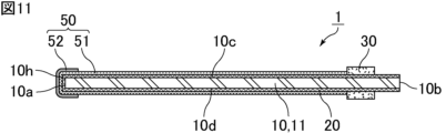
- 11 is a cross-sectional view of the electrolytic capacitor element shown in FIG. 9 taken along line FF.
- FIG. 12 is a perspective view schematically showing an example of an electrolytic capacitor element according to still another embodiment of the invention.
- 13 is a cross-sectional view of the electrolytic capacitor element shown in FIG. 12 along line GG.
- 14 is a cross-sectional view of the electrolytic capacitor element shown in FIG. 12 taken along line HH.
- FIG. 15 is an enlarged cross-sectional view of the mask layer portion of the electrolytic capacitor element shown in FIG. 2.
- FIG. FIG. 16 is a schematic diagram showing an example of a process of preparing a valve metal substrate on which a mask layer is formed.
- FIG. 17 is a schematic diagram showing an example of the process of forming the first layer of the solid electrolyte layer.
- FIG. 18 is a schematic diagram showing an example of the process of forming the second layer of the solid electrolyte layer.
- FIG. 19 is a perspective view schematically showing an example of an electrolytic capacitor including an electrolytic capacitor element according to an embodiment of the invention. 20 is a cross-sectional view of the electrolytic capacitor shown in FIG. 19 taken along line ZZ.
- the electrolytic capacitor element of the present invention will be described below.
- the present invention is not limited to the following configurations, and can be appropriately modified and applied without changing the gist of the present invention. Combinations of two or more of the individual desirable configurations described below are also part of the present invention.
- FIG. 1 is a plan view schematically showing an example of an electrolytic capacitor element according to an embodiment of the invention.
- FIG. 2 is a cross-sectional view of the electrolytic capacitor element shown in FIG. 1 along line XX. Note that in FIG. 1, the solid electrolyte layer 50 covered with the conductive layer 60 is indicated by a dashed line. 1 and 2 show the solid electrolyte layer 50 without distinguishing the first layer 51 and the second layer 52 from each other.
- the electrolytic capacitor element 1 shown in FIGS. 1 and 2 is a solid electrolytic capacitor element, which is composed of a valve action metal substrate 11, an anode 10 having a distal end surface 10a and a proximal end surface 10b, and an anode 10 except for the proximal end surface 10b.
- FIG. 3 is a perspective view of the electrolytic capacitor element shown in FIG. 4 is a cross-sectional view of the electrolytic capacitor element shown in FIG. 3 along line AA.
- FIG. 5 is a cross-sectional view of the electrolytic capacitor element shown in FIG. 3 along line BB.
- 3 4 and 5 show the state before the conductive layer 60 of the cathode 40 is formed. 3, the illustration of the dielectric layer 20 is omitted, and the first layer 51 of the solid electrolyte layer 50 is indicated by a dashed line, showing the first layer 51 as seen through.
- the solid electrolyte layer 50 includes a first layer 51 including a first conductive polymer doped with a first dopant and a first layer 51 including a first conductive polymer doped with a second dopant. and a second layer 52 containing a second conductive polymer, the second layer 52 being partially arranged in the plane of the solid electrolyte layer 50, and the first layer 51 being the solid electrolyte It is arranged at least in a region where the second layer 52 is not arranged in the plane of the layer 50 .
- the second conductive polymer is more likely to be dedoped than the first conductive polymer.
- leakage current can be suppressed while suppressing an increase in the equivalent series resistance of the electrolytic capacitor element 1 .
- the reason (action) that this effect is obtained is considered as follows. That is, it is considered that dedoping of the conductive polymer occurs locally at the location where the leakage current occurs, and the conductive polymer can be insulated.
- the second layer 52 containing the second conductive polymer, which is likely to be dedoped is partially arranged in the plane of the solid electrolyte layer 50, a leakage current is generated.
- the second layer 52 can be selectively arranged in a place where it is easy to leak, and as a result, leakage current is suppressed by insulating the second conductive polymer.
- the second layer 52 can function as a local self-healing layer.
- conductive polymers which are generally susceptible to dedoping, have relatively poor conductivity, and therefore tend to increase the equivalent series resistance of electrolytic capacitor elements.
- the second layer 52 which may lead to an increase in equivalent series resistance, is partially arranged in the plane of the solid electrolyte layer 50, while the second conductive polymer
- the second conductive polymer is more likely to be undoped than the first conductive polymer
- the second main chain of the second conductive polymer and the second dopant is smaller than that between the first main chain of the first conductive polymer and the first dopant.
- the occurrence of leakage current may interfere with the electrical coupling between the main chain of the conductive polymer and the dopant, or the leakage current may It is thought that dedoping occurs when the dopant undergoes thermal motion due to the Joule heat generated when the dopant flows into the conductive polymer.
- the term "conductive polymer” includes a main chain and a dopant. That is, the first conductive polymer includes a first main chain and a first dopant, and the second conductive polymer includes a second main chain and a second dopant.
- the anode 10 has six surfaces: a distal end surface 10a, a proximal end surface 10b, a pair of main surfaces 10c and 10d, and a pair of side surfaces 10e and 10f, It has corners where three of these six faces intersect and ridges where two of these six faces intersect, and the second layer 52 covers each corner 10g by the tip face 10a. ing. Since leakage current is generally likely to occur at the corners of the anode, this makes it possible to more effectively suppress the leakage current.
- FIG. 6 is a perspective view schematically showing an example of an electrolytic capacitor element according to another embodiment of the invention.
- 7 is a cross-sectional view of the electrolytic capacitor element shown in FIG. 6 along line CC.
- 8 is a cross-sectional view of the electrolytic capacitor element shown in FIG. 6 taken along line DD.
- 6, 7 and 8 show the state before the conductive layer 60 of the cathode 40 is formed. 6, the illustration of the dielectric layer 20 is omitted, and the first layer 51 of the solid electrolyte layer 50 is indicated by a dashed line, showing the first layer 51 as seen through.
- the second layer 52 may further cover the tip surface 10a and each ridge line portion 10h formed by the tip surface 10a. Since leakage current is generally likely to occur even at the ridge of the anode, this can further effectively suppress the leakage current. In addition, it is easier to form the second layer 52 in the case shown in FIG. 3 than in the case shown in FIG.
- a corner portion is a portion where three surfaces intersect, and a ridge portion is a portion where two surfaces intersect.
- a corner portion formed by a certain surface means a corner portion where three surfaces including the surface intersect, and a ridge portion formed by a surface means a ridge portion where two surfaces including the surface intersect.
- FIG. 9 is a perspective view schematically showing an example of an electrolytic capacitor element according to still another embodiment of the invention.
- 10 is a cross-sectional view of the electrolytic capacitor element shown in FIG. 9 taken along line EE.
- 11 is a cross-sectional view of the electrolytic capacitor element shown in FIG. 9 taken along line FF.
- 10 and 11 show the state before the conductive layer 60 of the cathode 40 is formed. 9, the illustration of the dielectric layer 20 is omitted, and the first layer 51 of the solid electrolyte layer 50 is indicated by a dashed line, showing the first layer 51 as seen through.
- the second layer 52 may further cover the side surfaces 10e and 10f and the ridgeline portions 10j formed by the side surfaces 10e and 10f. Thereby, leakage current can be suppressed particularly effectively.
- FIG. 12 is a perspective view schematically showing an example of an electrolytic capacitor element according to still another embodiment of the invention.
- 13 is a cross-sectional view of the electrolytic capacitor element shown in FIG. 12 along line GG.
- 14 is a cross-sectional view of the electrolytic capacitor element shown in FIG. 12 taken along line HH. 12, 13 and 14 show the state before the conductive layer 60 of the cathode 40 is formed.
- the illustration of the dielectric layer 20 is omitted, and the first layer 51 of the solid electrolyte layer 50 is indicated by a dashed line, showing a state in which the first layer 51 is seen through.
- the second layer 52 may be arranged along the mask layer 30, as shown in FIGS.
- the thickness of the solid electrolyte layer becomes thin along the mask layer, and as a result, leakage current may occur. It is possible to effectively suppress the leakage current at the location.
- a second layer having both the structure shown in FIG. 3, 6 or 9 and the structure shown in FIG. 12 may be formed. That is, for example, by combining the structures shown in FIGS. 6 and 12, the second layer 52 covers each corner 10g formed by the tip surface 10a, the tip surface 10a, and each ridgeline portion 10h formed by the tip surface 10a. , may be arranged along the mask layer 30 .
- the anode 10 is a square-shaped thin film (foil) formed from the valve action metal base 11, and preferably has a rectangular shape (strip shape) having a pair of long sides and a pair of short sides.
- the distal end surface 10a and the proximal end surface 10b are end surfaces located on a pair of sides (preferably a pair of short sides) of the anode 10, and the proximal end surface 10b is an exposed end surface not covered with the dielectric layer 20, It is exposed at one end face of the electrolytic capacitor and connected to an external electrode which will be described later.
- the anode 10 has a distal end surface 10a, a proximal end surface 10b, main surfaces 10c and 10d, and side surfaces 10e and 10f.
- planar view means viewing from the direction normal to the main surface of the anode (valve action metal substrate).
- FIG. 15 is an enlarged cross-sectional view of the mask layer portion of the electrolytic capacitor element shown in FIG.
- each main surface of the valve action metal substrate 11 (anode 10) is provided with a plurality of recesses. Therefore, each main surface of the valve metal substrate 11 is porous. As a result, the surface area of the valve metal substrate 11 is increased. Both main surfaces of the valve action metal substrate 11 are not limited to being porous, and only one of the two main surfaces of the valve action metal substrate 11 may be porous.
- the valve action metal substrate 11 is made of, for example, a single metal such as aluminum, tantalum, niobium, titanium, or zirconium, or a valve action metal such as an alloy containing these metals.
- An oxide film can be formed on the surface of the valve metal.
- the valve action metal substrate 11 may be composed of a core portion and a porous portion provided on at least one main surface of the core portion.
- a porous fine powder sintered body or the like can be used as appropriate.
- Dielectric layer 20 is provided here on the surface of anode 10 except for base end surface 10b. That is, the dielectric layer 20 is provided on the distal end surface 10a, the main surfaces 10c and 10d, and the side surfaces 10e and 10f of the anode 10, while the dielectric layer 20 is provided on the proximal end surface 10b of the anode 10. not However, dielectric layer 20 may be provided on at least one of major surfaces 10c and 10d of anode 10 except for base end surface 10b.
- the dielectric layer 20 is preferably composed of an oxide film provided on the surface of the valve action metal substrate 11 .
- dielectric layer 20 is composed of an oxide of aluminum.
- the oxide of aluminum is formed by anodizing the surface of the valve action metal substrate 11, as will be described later.
- the mask layer 30 is a linear (extending in a strip) insulating member provided on the dielectric layer 20 along the base end surface 10b of the anode 10, preferably along the short side of the anode 10, It separates the anode 10 and the cathode 40 to ensure insulation therebetween.
- the mask layer 30 divides the anode 10 into a region on the side of the proximal end surface 10b and a region on the side of the distal end surface 10a.
- the mask layer 30 is arranged at a predetermined distance from the base end surface 10b, but may be arranged up to the base end surface 10b.
- the mask layer 30 is provided on the main surfaces 10c and 10d and the side surfaces 10e and 10f of the anode 10 with the dielectric layer 20 interposed therebetween. It may be provided on at least one of 10c and 10d (however, the main surface on which dielectric layer 20 is provided).
- the mask layer 30 is preferably provided so as to fill a plurality of pores (concave portions) of the valve metal substrate 11 .
- the mask layer 30 only needs to partially cover the outer surface of the dielectric layer 20, and there may be pores (recesses) in the valve metal substrate 11 that are not filled with the mask layer 30. .
- the mask layer 30 is made of an insulating material.
- the mask layer 30 is formed, for example, by applying a mask material such as a composition containing an insulating resin.
- insulating resins include polyphenylsulfone (PPS), polyethersulfone (PES), cyanate ester resin, fluorine resin (tetrafluoroethylene, tetrafluoroethylene-perfluoroalkyl vinyl ether copolymer, etc.), and soluble polyimide.
- Compositions comprising siloxane and epoxy resins, polyimide resins, polyamideimide resins, derivatives or precursors thereof, and the like are included.
- the application of the mask material can be performed, for example, by screen printing, roller transfer, dispenser, inkjet printing, or the like.
- the cathode 40 has a solid electrolyte layer 50 provided on the dielectric layer 20 and a conductive layer 60 provided on the solid electrolyte layer 50 . Also, the cathode 40 is provided on the dielectric layer 20 on the tip surface 10 a side of the mask layer 30 . That is, it is provided on the dielectric layer 20 in a region on the tip surface 10 a side of the anode 10 partitioned by the mask layer 30 .
- the solid electrolyte layer 50 is provided on the dielectric layer 20 . As shown in FIG. 15 , the solid electrolyte layer 50 is preferably provided so as to fill a plurality of pores (recesses) of the valve metal substrate 11 . However, it is sufficient that a portion of the outer surface of the dielectric layer 20 is covered with the solid electrolyte layer 50, and there are pores (recesses) of the valve metal substrate 11 that are not filled with the solid electrolyte layer 50. good too.
- the solid electrolyte layer 50 is provided on the dielectric layer 20 on the tip surface 10 a side of the mask layer 30 . That is, it is provided on the dielectric layer 20 in a region on the tip surface 10 a side of the anode 10 partitioned by the mask layer 30 .
- the solid electrolyte layer 50 includes the first layer 51 containing the first conductive polymer doped with the first dopant and the second conductive polymer doped with the second dopant. a second layer 52 comprising; The second layer 52 is arranged only in a partial region of the plane of the solid electrolyte layer 50 instead of the entire region. That is, the second layer 52 is unevenly distributed not in the thickness direction of the solid electrolyte layer 50 but in the in-plane direction.
- the first layer 51 is arranged at least in a region in the plane of the solid electrolyte layer 50 where the second layer 52 is not arranged. Therefore, the solid electrolyte layer 50 has at least one of the first layer 51 and the second layer 52 arranged in its plane.
- the second layer 52 is arranged only on a part of the area on the first layer 51 .
- the thickness of the first layer 51 is not particularly limited, and may be approximately the same thickness as a general solid electrolyte layer, for example.
- the maximum thickness of the first layer 51 is preferably 2 ⁇ m or more and 50 ⁇ m or less, more preferably 3 ⁇ m or more and 40 ⁇ m or less, and even more preferably 5 ⁇ m or more and 30 ⁇ m or less.
- the thickness of the second layer 52 is also not particularly limited. More preferably, it is 5 ⁇ m or more and 30 ⁇ m or less.
- the location where the second layer 52 is arranged can be set as appropriate.
- a configuration in which the second layer 52 further covers the front end surface 10a of the anode 10 and each ridgeline portion 10h formed by the front end surface 10a (see FIG. 6, etc.); and each ridgeline portion 10j by each of the side surfaces 10e and 10f (see FIG. 9 etc.), and (4) a mode in which the second layer 52 is arranged along the mask layer 30 (see FIG. 12 etc.).
- the second layer 52 may cover at least one of the four corners 10g of the tip surface 10a, but preferably covers the four corners 10g.
- FIG. 3 shows a case where two corners 10g (vertical corners 10g in FIG. 3) formed by the same side surface 10e or 10f are independently covered with the second layer 52.
- the corner 10 g may be integrally covered with the second layer 52 . That is, the four ridgeline portions 10h formed by the tip surface 10a include two ridgeline portions 10ha formed by the side surface 10e or 10f and the tip surface 10a, but the second layer 52 may further cover the ridgeline portions 10ha.
- the second layer 52 may cover at least one of the four ridgeline portions 10h formed by the tip surface 10a, but preferably covers each of the four ridgeline portions 10h. In this way, the second layer 52 preferably covers the tip of the anode 10 (the part including the tip face 10a as a part). is preferably provided over each of the
- the second layer 52 may cover at least one of the two sides 10e and 10f, but preferably covers the two sides 10e and 10f respectively.
- the second layer 52 may cover at least one of the four ridgeline portions 10j formed by the side surfaces 10e and 10f, but preferably covers the four ridgeline portions 10j.
- the second layer 52 does not have to cover the tip end face 10a and the ridge line portions 10h formed by the tip end face 10a.
- the second layer 52 may be arranged along the mask layer 30 on at least one of the main surfaces 10c and 10d and the side surfaces 10e and 10f of the anode 10, although these are preferably arranged along the mask layer 30 on each side of the .
- the second layer 52 preferably fills the gap between the first layer 51 and the mask layer 30 .
- the shape of the second layer 52 is not particularly limited.
- a conductive polymer such as polypyrrole, polythiophene, or polyaniline is used as the material forming the solid electrolyte layer 50 .
- polythiophene is preferred, and poly(3,4-ethylenedioxythiophene) called PEDOT is particularly preferred.
- the conductive polymer contains a dopant such as polystyrene sulfonic acid (PSS).
- first conductive polymer first main chain and first dopant
- second conductive polymer second main chain
- the second dopant contained in the second conductive polymer preferably has a smaller molecular size than the first dopant contained in the first conductive polymer. As a result, the second conductive polymer can be dedoped more effectively than the first conductive polymer.
- the “molecular size” is the volume occupied by the molecular model that visualizes the electron density of each element that constitutes the dopant.
- the “molecular size” may be expressed as the diameter of a sphere having an equivalent volume to the volume occupied by the molecular model that visualizes the electron density.
- Suitable combinations of the first dopant and the second dopant include, for example, the following.
- the first dopant contained in the first conductive polymer may be p-toluenesulfonate ions
- the second dopant contained in the second conductive polymer may be sulfate ions
- first dopant contained in the first conductive polymer is an anthraquinonesulfonate ion
- the second dopant contained in the second conductive polymer is paratoluenesulfonate ion. good.
- first dopant contained in the first conductive polymer is polystyrene sulfonate ion
- the second dopant contained in the second conductive polymer is p-toluenesulfonate ion. good.
- the first dopant may be a molecule with more aromatic rings or a wider conjugated system than the second dopant.
- dedoping is more likely to occur and the molecular size is smaller in the order of polystyrene sulfonate ion, anthraquinone sulfonate ion, paratoluenesulfonate ion, and sulfate ion. Become.
- the second main chain contained in the second conductive polymer may have the same skeleton as the first main chain contained in the first conductive polymer.
- the first main chain and the second main chain may be polythiophene, and PEDOT is particularly preferred.
- the second main chain contained in the second conductive polymer may have a different skeleton from the first main chain contained in the first conductive polymer.
- the first main chain contained in the first conductive polymer is polythiophene (particularly preferably PEDOT), and the second main chain contained in the second conductive polymer is polypyrrole or polyaniline. good too.
- the solid electrolyte layer 50 is formed by depositing a conductive material such as poly(3,4-ethylenedioxythiophene) on the surface of the dielectric layer 20 using a liquid containing a polymerizable monomer such as 3,4-ethylenedioxythiophene. It is formed by a method of forming a polymeric film, a method of applying a dispersion of a conductive polymer such as poly(3,4-ethylenedioxythiophene) to the surface of the dielectric layer 20 and drying it, or the like. .
- each corner portion 10g and each ridge portion 10h of the anode 10 Since the thickness of the solid electrolyte layer 50 tends to be thin above 10j and above the mask layer 30, leakage current can be suppressed more effectively.
- the first layer 51 is preferably formed by forming an inner layer that fills the pores (recesses) of the valve action metal substrate 11 and then forming an outer layer that covers the entire dielectric layer 20 .
- the inner layer can be formed by, for example, a dipping method, sponge transfer, screen printing, dispenser, inkjet printing, or the like.
- the outer layer can be formed by, for example, a dipping method, sponge transfer, screen printing, dispenser, inkjet printing, or the like.
- the formation of the second layer 52 can be performed by, for example, an immersion method, sponge transfer, screen printing, dispenser, inkjet printing, etc. In the above cases (1), (3) and (4), Inkjet printing is preferred, and in the case of (2) above, immersion is preferred.
- the conductive layer 60 is provided on the solid electrolyte layer 50 .
- the conductive layer 60 covers substantially the entire solid electrolyte layer 50 and is in contact with the mask layer 30 . Note that the conductive layer 60 may be arranged up to the front of the mask layer 30 .
- the conductive layer 60 has a substantially constant thickness.
- the conductive layer 60 includes, for example, a carbon layer or a cathode conductor layer. Also, the conductive layer 60 may be a composite layer in which a cathode conductor layer is provided on the outer surface of a carbon layer, or a mixed layer containing carbon and a cathode conductor layer material.
- the carbon layer is formed, for example, by applying a carbon paste containing carbon particles and resin to the surface of the solid electrolyte layer 50 and drying it.
- the carbon paste can be applied by, for example, an immersion method, sponge transfer, screen printing, spray coating, dispenser, inkjet printing, or the like.
- the cathode conductor layer is formed, for example, by a method of applying a conductive paste containing metal particles such as gold, silver, copper, platinum, and a resin to the surface of the solid electrolyte layer or carbon layer and drying the paste.
- the cathode conductor layer is preferably a silver layer.
- the conductive paste can be applied by, for example, dipping, sponge transfer, screen printing, spray coating, dispenser, inkjet printing, or the like.
- FIG. 16 is a schematic diagram showing an example of a process of preparing a valve metal substrate on which a mask layer is formed.
- Valve action metal substrate 11A having a dielectric layer 20 on its surface is prepared.
- Valve action metal substrate 11A includes a plurality of element portions 12 and support portions 13 .
- Each element portion 12 is strip-shaped and protrudes from the support portion 13 .
- a mask layer 30 is formed on the dielectric layer 20 of each element portion 12 .
- valve action metal substrate 11A having a porous portion on its surface is cut by laser processing, punching, or the like to be processed into a shape including a plurality of element portions 12 and support portions 13 .
- mask layers 30 are formed on both main surfaces and both side surfaces of the element portions 12 along the short sides of each element portion 12 .
- valve action metal substrate 11A is anodized to form an oxide film that will become the dielectric layer 20 on the surface of the valve action metal substrate 11A.
- an oxide film is also formed on the side surfaces of the element portion 12 cut by laser processing, punching, or the like.
- a chemically processed foil on which an oxide of a valve action metal has already been formed may be used as the valve action metal substrate 11A.
- an oxide film is formed on the side surface of the cut element portion 12 by anodizing the cut valve metal substrate 11A.
- FIG. 17 is a schematic diagram showing an example of the process of forming the first layer of the solid electrolyte layer.
- a first layer 51 (see FIG. 3, etc.) of the solid electrolyte layer 50 is formed on the dielectric layer 20 of the element section 12 .
- FIG. 17 shows a state in which the processing liquid 70 for forming the first conductive polymer is being supplied to the processing tank 75 .
- a dispersion liquid of the first conductive polymer is used as the treatment liquid 70 for forming the first conductive polymer.
- a conductive polymer film can be formed by attaching the dispersion liquid of the first conductive polymer to the outer surface of the dielectric layer 20 and drying it.
- a liquid containing a polymerizable monomer such as 3,4-ethylenedioxythiophene and an oxidizing agent such as iron (III) p-toluenesulfonate. may be used.
- a liquid containing a polymerizable monomer can be attached to the outer surface of the dielectric layer 20 to form a conductive polymer film by chemical polymerization. This conductive polymer film becomes the first layer 51 of the solid electrolyte layer 50 .
- the treatment liquid 70 is impregnated into the porous portion of the valve action metal substrate 11A.
- the valve metal substrate 11A is pulled out of the treatment liquid 70 and dried at a predetermined temperature for a predetermined time.
- the first layer 51 of the solid electrolyte layer 50 is formed by repeating immersion in the treatment liquid 70 , pulling up, and drying a predetermined number of times.
- valve action metal substrate 11A is immersed in a first dispersion liquid containing a first conductive polymer (a liquid containing a polymerizable monomer may be used), pulled out, and then dried to form the first layer 51.
- a first conductive polymer a liquid containing a polymerizable monomer may be used
- An inner layer a portion provided on the dielectric layer 20 and filling the pores of the valve action metal substrate 11
- the immersion in the first dispersion, pulling up and drying may be performed multiple times.
- the primer layer may be formed by immersing the valve metal substrate 11A in a solution containing a primer compound, pulling it out, and drying it.
- valve action metal substrate 11A is immersed in a second dispersion containing a first conductive polymer (a liquid containing a polymerizable monomer may be used), pulled out, and then dried to form a first layer 51.
- a first conductive polymer a liquid containing a polymerizable monomer may be used
- the valve metal substrate 11A is washed with pure water to remove excess primer compound. After washing, a drying process is performed. As described above, the first layer 51 of the solid electrolyte layer 50 is formed in a predetermined region.
- FIG. 18 is a schematic diagram showing an example of the process of forming the second layer of the solid electrolyte layer.
- FIG. 18 shows a state in which the processing liquid 71 for forming the second conductive polymer is being supplied to the processing bath 76 .
- a dispersion liquid of the second conductive polymer is used as the treatment liquid 71 for forming the second conductive polymer.
- a conductive polymer film can be formed by attaching a dispersion liquid of the second conductive polymer to the outer surface of the first layer 51 and drying it.
- a liquid containing a polymerizable monomer such as 3,4-ethylenedioxythiophene and an oxidizing agent such as iron (III) p-toluenesulfonate. may be used.
- a liquid containing a polymerizable monomer can be attached to the outer surface of the first layer 51 to form a conductive polymer film by chemical polymerization. This conductive polymer film becomes the second layer 52 of the solid electrolyte layer 50 .
- the treatment liquid 71 adheres to the outer surface of the first layer 51 by immersing the tip of the valve action metal substrate 11A in the treatment liquid 71 . After being immersed for a predetermined time, the valve metal substrate 11A is pulled out of the treatment liquid 71 and dried at a predetermined temperature for a predetermined time.
- the second layer 52 of the solid electrolyte layer 50 as shown in FIG. 6 is formed by repeating immersion in the treatment liquid 71, pulling up and drying a predetermined number of times.
- a treatment liquid for forming the second conductive polymer for example, the second conductive polymer dispersion or a liquid containing a polymerizable monomer and an oxidizing agent
- the second layer 52 of the solid electrolyte layer 50 may be formed in a predetermined region by discharging onto the outer surface of the first layer 51 . Thereby, the second layer 52 of the solid electrolyte layer 50 as shown in FIGS. 3, 9 and 12 can be formed.
- valve metal substrate 11A is immersed in the carbon paste, pulled out, and dried to form a carbon layer in a predetermined region.
- valve action metal substrate 11A is immersed in a conductive paste containing metal particles such as silver paste, pulled out, and dried to form a cathode conductor layer in a predetermined region.
- valve action metal substrate 11A is cut to separate the element portion 12, thereby forming the strip-shaped anode 10 whose cut surface serves as the base end surface 10b.
- the electrolytic capacitor element 1 is obtained through the above steps.
- electrolytic capacitor An example of an electrolytic capacitor including the electrolytic capacitor element of the present invention will be described below. Note that the electrolytic capacitor element of the present invention may be included in electrolytic capacitors having other configurations. For example, lead frames may be used as external electrodes.
- the electrolytic capacitor may also include electrolytic capacitor elements other than the electrolytic capacitor element of the present invention (that is, electrolytic capacitor elements having a structure different from that of the electrolytic capacitor element of the present invention).
- FIG. 19 is a perspective view schematically showing an example of an electrolytic capacitor including an electrolytic capacitor element according to an embodiment of the invention. 20 is a cross-sectional view of the electrolytic capacitor shown in FIG. 19 taken along line ZZ.
- L indicates the length direction of the electrolytic capacitor 100 and the exterior body 110
- W indicates the width direction
- T indicates the height direction.
- the length direction L, the width direction W, and the height direction T are orthogonal to each other.
- the electrolytic capacitor 100 has a substantially rectangular parallelepiped outer shape.
- the electrolytic capacitor 100 is a solid electrolytic capacitor, and includes an exterior body 110 , a first external electrode 120 , a second external electrode 130 , and a plurality of electrolytic capacitor elements 1 .
- the exterior body 110 seals a plurality of electrolytic capacitor elements 1 . That is, a plurality of electrolytic capacitor elements 1 are embedded in the exterior body 110 . Note that the exterior body 110 may seal one electrolytic capacitor element 1 . That is, one electrolytic capacitor element 1 may be embedded inside the exterior body 110 .
- the exterior body 110 has a substantially rectangular parallelepiped outer shape.
- the exterior body 110 has a first major surface 110a and a second major surface 110b that face each other in the height direction T, a first side face 110c and a second side face 110d that face each other in the width direction W, and a first side face 110c and a second side face 110d that face each other in the length direction L. It has one end face 110e and a second end face 110f.
- the exterior body 110 has a substantially rectangular parallelepiped outer shape, and it is preferable that the corners and ridges are rounded.
- the exterior body 110 is made of sealing resin, for example.
- the sealing resin contains at least resin, and preferably contains resin and filler.
- epoxy resin epoxy resin, phenol resin, polyimide resin, silicone resin, polyamide resin, liquid crystal polymer, etc. are preferably used.
- Silica particles, alumina particles, etc. are preferably used as the filler.
- a material containing solid epoxy resin, phenol resin, and silica particles is preferably used as the sealing resin.
- resin molds such as compression molds and transfer molds are preferably used, and compression molds are more preferably used.
- molding methods such as a dispensing method and a printing method are preferably used. Among them, it is preferable to seal the periphery of the electrolytic capacitor element 1 with a sealing resin by compression molding to form the exterior body 110 .
- the exterior body 110 may be composed of a substrate and a sealing resin provided on the substrate.
- the substrate is, for example, an insulating resin substrate such as a glass epoxy substrate.
- the bottom surface of the substrate constitutes the second main surface 110b of the exterior body 110.
- the thickness of the substrate is, for example, 100 ⁇ m.
- a plurality of electrolytic capacitor elements 1 are stacked in the height direction T with conductive adhesive 140 interposed therebetween.
- the extension direction of each of the plurality of electrolytic capacitor elements 1 is substantially parallel to the first main surface 110 a and the second main surface 110 b of the outer package 110 .
- Electrolytic capacitor elements 1 are bonded to each other via conductive adhesive 140 .
- the conductive adhesive 140 contains, for example, metal particles such as gold, silver, copper, platinum, etc., and resin.
- metal particles such as gold, silver, copper, platinum, etc.
- resin such as gold, silver, copper, platinum, etc.
- silver is used as the metal particles
- acrylic resin is used as the resin.
- Other examples of the resin contained in the conductive adhesive 140 include urethane resin, epoxy resin, polyimide resin, phenol resin, and the like.
- the first external electrode 120 is provided on the first end face 110e of the exterior body 110.
- the first external electrode 120 is provided from the first end surface 110e of the exterior body 110 over each of the first main surface 110a, the second main surface 110b, the first side surface 110c, and the second side surface 110d.
- First external electrode 120 is electrically connected to conductive layer 60 of cathode 40 of electrolytic capacitor element 1 exposed from exterior body 110 at first end face 110e.
- the first external electrode 120 may be directly or indirectly connected to the conductive layer 60 on the first end face 110 e of the outer casing 110 .
- the second external electrode 130 is provided on the second end face 110f of the exterior body 110.
- the second external electrode 130 is provided from the second end surface 110f of the exterior body 110 over each of the first main surface 110a, the second main surface 110b, the first side surface 110c, and the second side surface 110d.
- Second external electrode 130 is electrically connected to anode 10 (valve metal substrate 11) of electrolytic capacitor element 1 exposed from exterior body 110 at second end surface 110f.
- the second external electrode 130 may be directly or indirectly connected to the anode 10 (valve metal substrate 11 ) at the second end surface 110 f of the exterior body 110 .
- the first external electrode 120 and the second external electrode 130 are each formed by a dip coating method, a screen printing method, a transfer method, an inkjet printing method, a dispensing method, a spray coating method, a brush coating method, a drop casting method, an electrostatic coating method, It is preferably formed by at least one method selected from the group consisting of plating and sputtering.
- the first external electrode 120 preferably has a resin electrode layer containing a conductive component and a resin component. Since the first external electrode 120 contains a resin component, the adhesion between the first external electrode 120 and the sealing resin of the exterior body 110 is enhanced, thereby improving the reliability.
- the second external electrode 130 preferably has a resin electrode layer containing a conductive component and a resin component. Since the second external electrode 130 contains a resin component, the adhesion between the second external electrode 130 and the sealing resin of the exterior body 110 is enhanced, thereby improving the reliability.
- the conductive component preferably contains, as a main component, an elemental metal such as silver, copper, nickel, or tin, or an alloy containing at least one of these metals.
- the resin component preferably contains epoxy resin, phenol resin, etc. as the main component.
- the resin electrode layer is formed by methods such as dip coating, screen printing, transfer, inkjet printing, dispensing, spray coating, brush coating, drop casting, and electrostatic coating.
- the resin electrode layer is preferably a printed resin electrode layer formed by applying a conductive paste by screen printing.
- the resin electrode layer is formed by applying a conductive paste by a screen printing method, compared with the case where the resin electrode layer is formed by applying a conductive paste by a dip coating method, the first external electrode 120 And the second external electrode 130 tends to be flat. That is, the thicknesses of the first external electrode 120 and the second external electrode 130 tend to be uniform.
- both the first external electrode 120 and the cathode conductor layer contain a resin component, so reliability is improved. improves.
- At least one of the first external electrode 120 and the second external electrode 130 may have a so-called plated layer formed by a plating method.
- plating layers include zinc/silver/nickel layers, silver/nickel layers, nickel layers, zinc/nickel/gold layers, nickel/gold layers, zinc/nickel/copper layers, and nickel/copper layers.
- a copper plated layer, a nickel plated layer, and a tin plated layer are preferably provided in this order (or with the exception of some plated layers).
- At least one of the first external electrode 120 and the second external electrode 130 may have both a resin electrode layer and a plating layer.
- the second external electrode 130 may have a resin electrode layer connected to the anode 10 (valve metal substrate 11) and an outer plated layer provided on the surface of the resin electrode layer.
- the second external electrode 130 includes an inner plated layer connected to the anode 10 (valve metal substrate 11), a resin electrode layer provided to cover the inner plated layer, and a resin electrode layer provided on the surface of the resin electrode layer. and an outer plated layer.
- a first layer 51 may be formed.
- the outer layer (the inner layer and the inner layer) is formed. It is preferably formed by forming a portion that is connected and covers the entire dielectric layer 20 in that region.
- the electrolytic capacitor element 1 is a solid electrolytic capacitor using a conductive polymer as an electrolyte material.
- a so-called hybrid type electrolytic capacitor element may be used in which an electrolytic solution is used together with the solid electrolyte.
- the electrolytic capacitor element 1 is used in the chip-type electrolytic capacitor 100 has been described, but the electrolytic capacitor element of the present invention can be used by being embedded in a package substrate included in a semiconductor device, for example.
- semiconductor devices include semiconductor composite devices in which a voltage regulator (voltage control device) and a load are mounted on a package substrate.
- Example 1 An aluminum foil having an etching layer on its surface was prepared as an anode (valve metal substrate), and immersed in an ammonium adipate aqueous solution for anodization to form a dielectric layer on the surface of the aluminum foil.
- a mask layer is formed on both main surfaces and both side surfaces of the foil through the dielectric layer by roller-transferring a composition comprising a soluble polyimidesiloxane and an epoxy resin onto the aluminum foil having the dielectric layer formed on the surface. formed.
- p-toluenesulfonate ions are incorporated into the first layer from iron (III) p-toluenesulfonate, which is an oxidizing agent used in the chemical polymerization reaction, to form the first dopant.
- a second layer of the solid electrolyte layer was partially formed on the first layer (see FIG. 6).
- the second main chain of the second layer was poly(3,4-ethylenedioxythiophene) and the second dopant of the second layer was sulfate ion. Sulfate ions from ammonium persulfate serve as the second dopant.
- an electrolytic capacitor element was obtained by sequentially forming a carbon layer and a silver layer.
- the resulting four electrolytic capacitor elements were laminated using a conductive adhesive to obtain a laminate. After that, the laminate was sealed with an epoxy resin and separated into pieces using a dicer. Next, a silver paste containing a resin component was screen-printed on the cathode-side and anode-side end surfaces of the solidified sealing body to form external electrodes on the cathode and anode, thereby obtaining a finished electrolytic capacitor.
- Example 2 A finished electrolytic capacitor was obtained in the same manner as in Example 1, except that the solid electrolyte layer was formed as follows.
- an aluminum foil having a dielectric layer formed on its surface is immersed in an aqueous dispersion of poly(3,4-ethylenedioxythiophene) and polystyrene sulfonic acid, pulled out, and then dried to form a dielectric layer.
- a first layer of a solid electrolyte layer was formed on the substrate.
- the first main chain of the first layer was poly(3,4-ethylenedioxythiophene), and the first dopant of the first layer was polystyrene sulfonate ion.
- para-toluenesulfonate ions are taken into the second layer from iron (III) para-toluenesulfonate, which is an oxidizing agent used in the chemical polymerization reaction, to 2 as a dopant.
- Example 3 A finished electrolytic capacitor was obtained in the same manner as in Example 1, except that the solid electrolyte layer was formed as follows.
- an aluminum foil having a dielectric layer formed on its surface is immersed in an aqueous dispersion of poly(3,4-ethylenedioxythiophene) and polystyrene sulfonic acid, pulled out, and then dried to form a dielectric layer.
- a first layer of a solid electrolyte layer was formed on the substrate.
- the first main chain of the first layer was poly(3,4-ethylenedioxythiophene), and the first dopant of the first layer was polystyrene sulfonate ion.
- NMP N-methyl-2-pyrrolidone
- Example 4 A finished electrolytic capacitor was obtained in the same manner as in Example 1, except that the solid electrolyte layer was formed as follows.
- an aluminum foil having a dielectric layer formed on its surface is immersed in an aqueous dispersion of poly(3,4-ethylenedioxythiophene) and polystyrene sulfonic acid, pulled out, and then dried to form a dielectric layer.
- a first layer of a solid electrolyte layer was formed on the substrate.
- the first main chain of the first layer was poly(3,4-ethylenedioxythiophene), and the first dopant of the first layer was polystyrene sulfonate ion.
- NMP N-methyl-2-pyrrolidone
- Example 1 A finished electrolytic capacitor was obtained in the same manner as in Example 1, except that the solid electrolyte layer was formed as follows.
- an aluminum foil having a dielectric layer formed on its surface is immersed in a mixed solution of iron (III) p-toluenesulfonate, 3,4-ethylenedioxythiophene and 1-butanol, pulled out, and then dried.
- a first layer of a solid electrolyte layer was formed on the dielectric layer.
- the first main chain of the first layer was poly(3,4-ethylenedioxythiophene), and the first dopant of the first layer was p-toluenesulfonate ion.
- a second layer of the solid electrolyte layer was not formed.
- Example 2 A finished electrolytic capacitor was obtained in the same manner as in Example 1, except that the solid electrolyte layer was formed as follows.
- an aluminum foil having a dielectric layer formed on its surface is immersed in a mixed solution of iron (III) p-toluenesulfonate, 3,4-ethylenedioxythiophene and 1-butanol, pulled out, and then dried.
- a first layer of a solid electrolyte layer was formed on the dielectric layer.
- the first main chain of the first layer was poly(3,4-ethylenedioxythiophene), and the first dopant of the first layer was p-toluenesulfonate ion.
- an aluminum foil is immersed in an aqueous ammonium persulfate solution so as to cover the entire first layer, pulled out, immersed in a mixed solution of 3,4-ethylenedioxythiophene and ethanol, pulled out, and dried.
- the second layer of the solid electrolyte layer was formed over the entire area of the first layer.
- the second main chain of the second layer was poly(3,4-ethylenedioxythiophene) and the second dopant of the second layer was sulfate ion.
- Example 3 A finished electrolytic capacitor was obtained in the same manner as in Example 1, except that the solid electrolyte layer was formed as follows.
- an aluminum foil having a dielectric layer formed on its surface is immersed in an aqueous dispersion of poly(3,4-ethylenedioxythiophene) and polystyrene sulfonic acid, pulled out, and then dried to form a dielectric layer.
- a first layer of a solid electrolyte layer was formed on the substrate.
- the first main chain of the first layer was poly(3,4-ethylenedioxythiophene), and the first dopant of the first layer was polystyrene sulfonate ion.
- a second layer of the solid electrolyte layer was not formed.
- Example 4 A finished electrolytic capacitor was obtained in the same manner as in Example 1, except that the solid electrolyte layer was formed as follows.
- an aluminum foil having a dielectric layer formed on its surface is immersed in an aqueous dispersion of poly(3,4-ethylenedioxythiophene) and polystyrene sulfonic acid, pulled out, and then dried to form a dielectric layer.
- a first layer of a solid electrolyte layer was formed on the substrate.
- the first main chain of the first layer was poly(3,4-ethylenedioxythiophene), and the first dopant of the first layer was polystyrene sulfonate ion.
- NMP N-methyl-2-pyrrolidone
- ESR equivalent series resistance
- LC leakage current
- Example 1 the second layer of the solid electrolyte layer covering the tip (including each corner) of the aluminum foil is doped with sulfate ions that are likely to cause dedoping. Good product rate is improving.
- the second layer of the solid electrolyte layer which selectively covers only the corners of the tip of the aluminum foil where leakage current is likely to occur, is doped with a dopant that is likely to cause dedoping. Therefore, a high LC good product rate is achieved while suppressing an increase in ESR.
- Electrolytic capacitor element 10 anode 10a tip surface 10b base end surface 10c, 10d main surface 10e, 10f side surface 10g corner portions 10h, 10ha, 10j edge portion 11, 11A valve action metal substrate 12 element portion 13 support portion 20 dielectric layer 30 mask Layer 40
- Cathode 50 Solid electrolyte layer 51 First layer 52 Second layer 60 Conductive layer 70, 71 Treatment liquid 75, 76 Treatment tank 100
Abstract
電解コンデンサ素子1は、弁作用金属基体11から構成され、先端面10a及び基端面10bを有する陽極10と、少なくとも基端面10bを除いて陽極10の少なくとも一方の主面10c、10d上に設けられた誘電体層20と、絶縁材料から構成され、基端面10bに沿って誘電体層20上に設けられたマスク層30と、マスク層30よりも先端面10a側において誘電体層20上に設けられた陰極40と、を備え、陰極40は、誘電体層20上に設けられた固体電解質層50と、固体電解質層50上に設けられた導電層60と、を有し、固体電解質層50は、第1のドーパントがドーピングされた第1の導電性高分子を含む第1層51と、第2のドーパントがドーピングされた第2の導電性高分子を含む第2層52と、を含み、第2層52は、固体電解質層50の面内において部分的に配置されており、第1層51は、固体電解質層50の面内において第2層52が配置されていない領域に少なくとも配置されており、第2の導電性高分子は、第1の導電性高分子よりも脱ドープが生じやすい。
Description
本発明は、電解コンデンサ素子に関する。
特許文献1には、陽極体表面に形成された第一の酸化物誘電体層と、陽極体の切断による露出端面に形成された第二の酸化物誘電体層と、第一の酸化物誘電体層上に形成された第一の導電性高分子層と、第二の酸化物誘電体層上に形成された第二の導電性高分子層とを有する固体電解コンデンサが開示されており、第二の導電性高分子層は第一の導電性高分子層よりも絶縁化しやすいことが記載されている。
特許文献1では、陽極体の切断面に形成された耐電圧の低い第二の酸化物誘電体層を第二の導電性高分子層で覆うことにより、第二の導電性高分子層が絶縁化されるため、容量の減少なしに漏れ電流の不良率の小さい固体電解コンデンサを提供することができる、としている。しかしながら、絶縁化のメカニズムが明確ではなく、かつ第二の導電性高分子層を絶縁化しやすくするための方策が絶縁性のバインダーの添加であるために、第二の導電性高分子層全体の導電性が下がり等価直列抵抗(ESR)の増大をまねくという点で改善の余地があった。また、電圧印加時に電界の集中しやすい箇所、例えば角部が第二の導電性高分子層で覆われていないため、漏れ電流の低減が充分ではないという点でもさらなる工夫の余地があった。
本発明は、上記の問題を解決するためになされたものであり、等価直列抵抗の増大を抑制しつつ漏れ電流の抑制が可能な電解コンデンサ素子を提供することを目的とする。
本発明の電解コンデンサ素子は、弁作用金属基体から構成され、先端面及び基端面を有する陽極と、少なくとも上記基端面を除いて上記陽極の少なくとも一方の主面上に設けられた誘電体層と、絶縁材料から構成され、上記基端面に沿って上記誘電体層上に設けられたマスク層と、上記マスク層よりも上記先端面側において上記誘電体層上に設けられた陰極と、を備え、上記陰極は、上記誘電体層上に設けられた固体電解質層と、上記固体電解質層上に設けられた導電層と、を有し、上記固体電解質層は、第1のドーパントがドーピングされた第1の導電性高分子を含む第1層と、第2のドーパントがドーピングされた第2の導電性高分子を含む第2層と、を含み、上記第2層は、上記固体電解質層の面内において部分的に配置されており、上記第1層は、上記固体電解質層の面内において上記第2層が配置されていない領域に少なくとも配置されており、上記第2の導電性高分子は、上記第1の導電性高分子よりも脱ドープが生じやすい。
本発明によれば、等価直列抵抗の増大を抑制しつつ漏れ電流の抑制が可能な電解コンデンサ素子を提供することができる。
以下、本発明の電解コンデンサ素子について説明する。
しかしながら、本発明は、以下の構成に限定されるものではなく、本発明の要旨を変更しない範囲において適宜変更して適用することができる。なお、以下において記載する個々の望ましい構成を2つ以上組み合わせたものもまた本発明である。
しかしながら、本発明は、以下の構成に限定されるものではなく、本発明の要旨を変更しない範囲において適宜変更して適用することができる。なお、以下において記載する個々の望ましい構成を2つ以上組み合わせたものもまた本発明である。
また、以下に示す各実施形態は例示であり、異なる実施形態で示した構成の部分的な置換又は組み合わせが可能であることは言うまでもない。複数の実施形態で共通の事項についての記述の繰り返しは省略し、異なる点についてのみ説明する。
[電解コンデンサ素子]
図1は、本発明の実施形態に係る電解コンデンサ素子の一例を模式的に示す平面図である。図2は、図1に示す電解コンデンサ素子のX-X線に沿った断面図である。なお、図1では、導電層60に覆われた固体電解質層50を破線で示す。また、図1及び図2では、第1層51及び第2層52を区別せずに固体電解質層50を示す。
図1は、本発明の実施形態に係る電解コンデンサ素子の一例を模式的に示す平面図である。図2は、図1に示す電解コンデンサ素子のX-X線に沿った断面図である。なお、図1では、導電層60に覆われた固体電解質層50を破線で示す。また、図1及び図2では、第1層51及び第2層52を区別せずに固体電解質層50を示す。
図1及び図2に示す電解コンデンサ素子1は、固体電解コンデンサ素子であり、弁作用金属基体11から構成され、先端面10a及び基端面10bを有する陽極10と、基端面10bを除いて陽極10の表面上に設けられた誘電体層20と、絶縁材料から構成され、基端面10bに沿って誘電体層20上に設けられたマスク層30と、マスク層30よりも先端面10a側において誘電体層20上に設けられた陰極40と、を備えており、陰極40は、誘電体層20上に設けられた固体電解質層50と、固体電解質層50上に設けられた導電層60と、を有している。
図3は、図1に示す電解コンデンサ素子の斜視図である。図4は、図3に示す電解コンデンサ素子のA-A線に沿った断面図である。図5は、図3に示す電解コンデンサ素子のB-B線に沿った断面図である。なお、図3、図4及び図5では、陰極40の導電層60を形成する前の状態を示す。また、図3では、誘電体層20の図示を省略し、また、固体電解質層50の第1層51を一点鎖線で示し、第1層51を透視した状態を示す。
図3、図4及び図5に示すように、固体電解質層50は、第1のドーパントがドーピングされた第1の導電性高分子を含む第1層51と、第2のドーパントがドーピングされた第2の導電性高分子を含む第2層52と、を含んでおり、第2層52は、固体電解質層50の面内において部分的に配置されており、第1層51は、固体電解質層50の面内において第2層52が配置されていない領域に少なくとも配置されている。そして、第2の導電性高分子は、第1の導電性高分子よりも脱ドープが生じやすい。
これにより、電解コンデンサ素子1の等価直列抵抗の増大を抑制しつつ漏れ電流の抑制が可能である。この効果が得られる理由(作用)については以下が考えられる。
すなわち、漏れ電流が発生した箇所では局所的に導電性高分子の脱ドープが発生して当該導電性高分子が絶縁化し得ると考えられる。そして、電解コンデンサ素子1では、脱ドープが生じやすい第2の導電性高分子を含む第2層52が、固体電解質層50の面内において部分的に配置されていることから、漏れ電流が発生しやすい箇所に第2層52を選択的に配置でき、その結果として第2の導電性高分子の絶縁化により漏れ電流が抑制される。すなわち、第2層52が局所的なセルフヒーリング層として機能し得る。一方、一般的に脱ドープが生じやすい導電性高分子は、相対的に導電性に劣るため、電解コンデンサ素子の等価直列抵抗の増大をまねく傾向にある。しかしながら、電解コンデンサ素子1では、等価直列抵抗の増大をまねく可能性のある第2層52は、固体電解質層50の面内において部分的に配置されており、他方、第2の導電性高分子に比べて相対的に脱ドープが生じにくい、すなわち等価直列抵抗の増大を抑制可能な第1の導電性高分子を含む第1層51が、固体電解質層50の面内において第2層52が配置されていない領域に少なくとも配置されているため、電解コンデンサ素子1全体の等価直列抵抗の上昇は防止される。以上より、電解コンデンサ素子1全体の等価直列抵抗の上昇を伴うことなく漏れ電流が低減できると考えられる。
ここで、「第2の導電性高分子は、第1の導電性高分子よりも脱ドープが生じやすい」とは、第2の導電性高分子の第2の主鎖と第2のドーパントとの間の結合力が、第1の導電性高分子の第1の主鎖と第1のドーパントとの間の結合力より小さいことを表している。
なお、漏れ電流による導電性高分子の脱ドープの発生メカニズムについては、漏れ電流が発生することで、導電性高分子の主鎖とドーパントとの間の電気的結合が阻害されたり、あるいは漏れ電流が導電性高分子に流れる際に発生するジュール熱によってドーパントが熱運動を起こしたりすることによって脱ドープが発生すると考えられる。
また、漏れ電流防止の観点のみからは、脱ドープが生じやすい第2の導電性高分子のみを固体電解質層50の面内全域に配置することも考えられるが、その場合、固体電解質層50全体の導電性が低下し、電解コンデンサ素子1の等価直列抵抗の増大をまねく可能性がある。また、脱ドープが生じやすい導電性高分子は、一般的に耐熱性が劣る傾向にあるため、脱ドープが生じやすい第2の導電性高分子のみを固体電解質層50の面内全域に配置すると、電解コンデンサ素子1の高温信頼性が低下する可能性がある。
このように、本明細書において、「導電性高分子」とは、主鎖及びドーパントを含んでいるものとする。すなわち、第1の導電性高分子は、第1の主鎖及び第1のドーパントを含み、第2の導電性高分子は、第2の主鎖及び第2のドーパントを含む。
図3、図4及び図5に示すように、陽極10は、先端面10aと、基端面10bと、一対の主面10c及び10dと、一対の側面10e及び10fとの6面を有し、これら6面のうちの3面が交わる角部と、これら6面のうちの2面が交わる稜線部と、を有しており、第2層52は、先端面10aによる各角部10gを覆っている。一般的に陽極の角部では漏れ電流が発生しやすいことから、これにより、漏れ電流をより効果的に抑制できる。
図6は、本発明の別の実施形態に係る電解コンデンサ素子の一例を模式的に示す斜視図である。図7は、図6に示す電解コンデンサ素子のC-C線に沿った断面図である。図8は、図6に示す電解コンデンサ素子のD-D線に沿った断面図である。なお、図6、図7及び図8では、陰極40の導電層60を形成する前の状態を示す。また、図6では、誘電体層20の図示を省略し、また、固体電解質層50の第1層51を一点鎖線で示し、第1層51を透視した状態を示す。
図6、図7及び図8に示すように、第2層52は、先端面10aと、先端面10aによる各稜線部10hと、をさらに覆っていてもよい。一般的に陽極の稜線部でも漏れ電流が発生しやすいことから、これにより、漏れ電流をさらに効果的に抑制できる。また、図6に示した場合に比べて、図3に示した場合の方が第2層52を形成しやすい。
なお、本明細書にて、角部とは、3面が交わる部分であり、稜線部とは、2面が交わる部分である。また、ある面による角部とは、その面を含む3面が交わる角部を意味し、ある面による稜線部とは、その面を含む2面が交わる稜線部を意味する。
図9は、本発明のさらに別の実施形態に係る電解コンデンサ素子の一例を模式的に示す斜視図である。図10は、図9に示す電解コンデンサ素子のE-E線に沿った断面図である。図11は、図9に示す電解コンデンサ素子のF-F線に沿った断面図である。なお、図9、図10及び図11では、陰極40の導電層60を形成する前の状態を示す。また、図9では、誘電体層20の図示を省略し、また、固体電解質層50の第1層51を一点鎖線で示し、第1層51を透視した状態を示す。
図9、図10及び図11に示すように、第2層52は、各側面10e、10fと、各側面10e、10fによる各稜線部10jと、をさらに覆っていてもよい。これにより、漏れ電流を特に効果的に抑制できる。
図12は、本発明のさらに別の実施形態に係る電解コンデンサ素子の一例を模式的に示す斜視図である。図13は、図12に示す電解コンデンサ素子のG-G線に沿った断面図である。図14は、図12に示す電解コンデンサ素子のH-H線に沿った断面図である。なお、図12、図13及び図14では、陰極40の導電層60を形成する前の状態を示す。また、図12では、誘電体層20の図示を省略し、また、固体電解質層50の第1層51を一点鎖線で示し、第1層51を透視した状態を示す。
図12、図13及び図14に示すように、第2層52は、マスク層30に沿って配置されてもよい。マスク層に沿った箇所では固体電解質層が薄くなり、その結果、漏れ電流が発生するおそれがあるが、第2層52がマスク層30に沿って配置されることにより、マスク層30に沿った箇所での漏れ電流を効果的に抑制可能である。
さらに、図示は省略するが、図3、図6又は図9に示した構造と、図12に示した構造とを併せ持つ第2層を形成してもよい。すなわち、例えば、図6及び図12に示した構造を組み合わせて、第2層52は、先端面10aによる各角部10gと、先端面10aと、先端面10aによる各稜線部10hとを覆うとともに、マスク層30に沿って配置されてもよい。
電解コンデンサ素子1における各構成について以下に詳しく説明する。
陽極10は、弁作用金属基体11から構成された平面視四角形状の薄膜(箔)であり、好ましくは、一対の長辺及び一対の短辺を有する平面視矩形状(短冊状)である。先端面10a及び基端面10bは、陽極10の一対の辺(好ましくは一対の短辺)に位置する端面であり、基端面10bは、誘電体層20で覆われていない露出した端面であり、電解コンデンサの一方の端面において露出して後述する外部電極に接続される。陽極10は、先端面10aと、基端面10bと、主面10c及び10dと、側面10e及び10fとを有している。
なお、本明細書にて、「平面視」とは、陽極(弁作用金属基体)の主面の法線方向から見ることを意味する。
図15は、図2に示す電解コンデンサ素子のマスク層部分を拡大した断面図である。
弁作用金属基体11(陽極10)の各主面には、図15に示すように、複数の凹部が設けられている。そのため、弁作用金属基体11の各主面は、多孔質状になっている。これにより、弁作用金属基体11の表面積が大きくなっている。なお、弁作用金属基体11の両主面が多孔質状である場合に限られず、弁作用金属基体11の両主面の一方のみが多孔質状であってもよい。
弁作用金属基体11は、例えば、アルミニウム、タンタル、ニオブ、チタン、ジルコニウム等の金属単体、又は、これらの金属を含む合金等の弁作用金属によって構成されている。弁作用金属の表面には、酸化被膜を形成することができる。
なお、弁作用金属基体11は、芯部と当該芯部の少なくとも一方の主面に設けられた多孔質部とによって構成されていればよく、金属箔の表面をエッチングしたもの、金属箔の表面に多孔質状の微粉焼結体を形成したもの等を適宜採用することができる。
誘電体層20は、ここでは、基端面10bを除いて陽極10の表面上に設けられている。すなわち、誘電体層20は、陽極10の先端面10a上と、主面10c及び10d上と、側面10e及び10f上とに設けられている一方で、陽極10の基端面10b上には設けられていない。
ただし、誘電体層20は、少なくとも基端面10bを除いて陽極10の主面10c及び10dの少なくとも一方上に設けられていればよい。
ただし、誘電体層20は、少なくとも基端面10bを除いて陽極10の主面10c及び10dの少なくとも一方上に設けられていればよい。
誘電体層20は、弁作用金属基体11の表面に設けられた酸化被膜によって構成されていることが好ましい。例えば、誘電体層20は、アルミニウムの酸化物で構成されている。アルミニウムの酸化物は、後述するように、弁作用金属基体11の表面が陽極酸化処理されることにより形成される。
マスク層30は、陽極10の基端面10bに沿って、好ましくは陽極10の短辺に沿って、誘電体層20上に設けられた直線状の(帯状に延在する)絶縁部材であり、陽極10と陰極40とを隔て、両者間の絶縁を確保している。マスク層30によって、陽極10は、基端面10b側の領域と、先端面10a側の領域とに区画されている。ここでは、マスク層30は、基端面10bから所定の間隔を空けて配置されているが、基端面10bの際まで配置されていてもよい。また、マスク層30は、誘電体層20を介して、陽極10の主面10c及び10d上と側面10e及び10f上に設けられているが、誘電体層20と同様に、陽極10の主面10c及び10dの少なくとも一方(ただし誘電体層20が設けられた主面)上に設けられていればよい。
図15に示すように、マスク層30は、弁作用金属基体11の複数の細孔(凹部)を充填するように設けられていることが好ましい。ただし、マスク層30によって誘電体層20の外表面の一部が覆われていればよく、マスク層30によって充填されていない弁作用金属基体11の細孔(凹部)が存在していてもよい。
マスク層30は、絶縁材料から構成されている。マスク層30は、例えば、絶縁性樹脂を含む組成物等のマスク材を塗布して形成される。絶縁性樹脂としては、例えば、ポリフェニルスルホン(PPS)、ポリエーテルスルホン(PES)、シアン酸エステル樹脂、フッ素樹脂(テトラフルオロエチレン、テトラフルオロエチレン・パーフルオロアルキルビニルエーテル共重合体等)、可溶性ポリイミドシロキサンとエポキシ樹脂からなる組成物、ポリイミド樹脂、ポリアミドイミド樹脂、及び、それらの誘導体又は前駆体等が挙げられる。
マスク材の塗布は、例えば、スクリーン印刷、ローラー転写、ディスペンサ、インクジェット印刷等により行うことができる。
陰極40は、誘電体層20上に設けられた固体電解質層50と、固体電解質層50上に設けられた導電層60と、を有している。また、陰極40は、マスク層30よりも先端面10a側において誘電体層20上に設けられている。すなわち、マスク層30によって区画された陽極10の先端面10a側の領域において誘電体層20上に設けられている。
固体電解質層50は、誘電体層20上に設けられている。図15に示すように、固体電解質層50は、弁作用金属基体11の複数の細孔(凹部)を充填するように設けられていることが好ましい。ただし、固体電解質層50によって誘電体層20の外表面の一部が覆われていればよく、固体電解質層50によって充填されていない弁作用金属基体11の細孔(凹部)が存在していてもよい。
固体電解質層50は、マスク層30よりも先端面10a側において誘電体層20上に設けられている。すなわち、マスク層30によって区画された陽極10の先端面10a側の領域において誘電体層20上に設けられている。
固体電解質層50は、上述のように、第1のドーパントがドーピングされた第1の導電性高分子を含む第1層51と、第2のドーパントがドーピングされた第2の導電性高分子を含む第2層52と、を含んでいる。
第2層52は、固体電解質層50の面内において全域ではなく部分的な領域のみに配置されている。すなわち、固体電解質層50の厚み方向ではなく面内方向において第2層52が偏在している。
他方、第1層51は、固体電解質層50の面内において第2層52が配置されていない領域に少なくとも配置されている。したがって、固体電解質層50は、その面内において第1層51及び第2層52の少なくとも一方が配置されている。
第2層52は、固体電解質層50の面内において全域ではなく部分的な領域のみに配置されている。すなわち、固体電解質層50の厚み方向ではなく面内方向において第2層52が偏在している。
他方、第1層51は、固体電解質層50の面内において第2層52が配置されていない領域に少なくとも配置されている。したがって、固体電解質層50は、その面内において第1層51及び第2層52の少なくとも一方が配置されている。
ここでは、図3等に示したように、第1層51は、固体電解質層50の面内の全域に配置されており、第2層52は、第1層51上に設けられている。すなわち、第2層52は、第1層51上の領域の一部のみに配置されている。
第1層51の厚みは、特に限定されず、例えば、一般的な固体電解質層と同程度の厚みであってもよい。具体的には、第1層51の最大厚みは、2μm以上、50μm以下であることが好ましく、3μm以上、40μm以下であることがより好ましく、5μm以上、30μm以下であることがさらに好ましい。
第2層52の厚みも、特に限定されないが、具体的には、第2層52の最大厚みは、2μm以上、50μm以下であることが好ましく、3μm以上、40μm以下であることがより好ましく、5μm以上、30μm以下であることがさらに好ましい。
第2層52が配置される箇所は適宜設定可能であるが、上述のように、(1)第2層52が陽極10の各角部10gを覆う形態(図3等参照)、(2)第2層52が陽極10の先端面10aと、先端面10aによる各稜線部10hと、をさらに覆う形態(図6等参照)、(3)第2層52が陽極10の各側面10e、10fと、各側面10e、10fによる各稜線部10jと、をさらに覆う形態(図9等参照)、(4)第2層52がマスク層30に沿って配置される形態(図12等参照)が好ましい。
(1)の場合、第2層52は、先端面10aによる4つの角部10gのうちの少なくとも1つを覆っていてもよいが、4つの角部10gをそれぞれ覆うことが好ましい。
また、図3には、同じ側面10e又は10fによる2つの角部10g(図3で上下に並ぶ角部10g)をそれぞれ独立して第2層52で覆う場合を示しているが、これら2つの角部10gを一体的に第2層52で覆ってもよい。すなわち、先端面10aによる4つの稜線部10hは、側面10e又は10fと先端面10aとによる2つの稜線部10haを含むが、第2層52は、稜線部10haをさらに覆っていてもよい。
また、図3には、同じ側面10e又は10fによる2つの角部10g(図3で上下に並ぶ角部10g)をそれぞれ独立して第2層52で覆う場合を示しているが、これら2つの角部10gを一体的に第2層52で覆ってもよい。すなわち、先端面10aによる4つの稜線部10hは、側面10e又は10fと先端面10aとによる2つの稜線部10haを含むが、第2層52は、稜線部10haをさらに覆っていてもよい。
(2)の場合、第2層52は、先端面10aによる4つの稜線部10hのうちの少なくとも1つを覆っていてもよいが、4つの稜線部10hをそれぞれ覆うことが好ましい。このように、第2層52は、陽極10の先端部(先端面10aを一部として含む部分)を覆うことが好ましく、先端面10aから、主面10c、主面10d、側面10e及び側面10fの各々に亘って設けられることが好ましい。
(3)の場合、第2層52は、2つの側面10e及び10fのうちの少なくとも1つを覆っていてもよいが、2つの側面10e及び10fをそれぞれ覆うことが好ましい。また、第2層52は、側面10e及び10fによる4つの稜線部10jのうちの少なくとも1つを覆っていてもよいが、4つの稜線部10jをそれぞれ覆うことが好ましい。
また、この場合、第2層52は、先端面10aと、先端面10aによる各稜線部10hと、を覆っていなくてもよい。
また、この場合、第2層52は、先端面10aと、先端面10aによる各稜線部10hと、を覆っていなくてもよい。
(4)の場合、第2層52は、陽極10の主面10c及び10dと、側面10e及び10fとのうちの少なくとも1つの面上においてマスク層30に沿って配置されてもよいが、これらの各面上においてマスク層30に沿って配置されることが好ましい。
また、この場合、第2層52とマスク層30との間には隙間が設けられていないことが好ましく、第2層52は、マスク層30に接触した状態でマスク層30と並んで配置されることが好ましい。
さらに、第1層51だけではマスク層30との間に隙間が発生することがあるが、第2層52は、第1層51とマスク層30との間のその隙間を埋めることが好ましい。
また、この場合、第2層52とマスク層30との間には隙間が設けられていないことが好ましく、第2層52は、マスク層30に接触した状態でマスク層30と並んで配置されることが好ましい。
さらに、第1層51だけではマスク層30との間に隙間が発生することがあるが、第2層52は、第1層51とマスク層30との間のその隙間を埋めることが好ましい。
なお、いずれの場合も第2層52の形状は特に限定されず、例えば、図3等に示したように互いに直交する複数の直線から周縁の輪郭線が構成される形状や、この形状において周縁の輪郭線のうちの少なくとも2つの直線が斜めに交わる形状、この形状において周縁の輪郭線のうちの少なくとも1つの直線が曲線になった形状等が挙げられる。
固体電解質層50を構成する材料としては、例えば、ポリピロール、ポリチオフェン、ポリアニリン等の導電性高分子が用いられる。これらの中では、ポリチオフェンが好ましく、PEDOTと呼ばれるポリ(3,4-エチレンジオキシチオフェン)が特に好ましい。また、上記導電性高分子は、ポリスチレンスルホン酸(PSS)等のドーパントを含んでいる。
ここで、第1層51に含まれる第1の導電性高分子(第1の主鎖及び第1のドーパント)と、第2層52に含まれる第2の導電性高分子(第2の主鎖及び第2のドーパント)の好適な例について説明する。
第2の導電性高分子に含まれる第2のドーパントは、第1の導電性高分子に含まれる第1のドーパントよりも分子サイズが小さいことが好ましい。これにより、第2の導電性高分子を第1の導電性高分子よりも効果的に脱ドープが生じやすくすることができる。
なお、ここで、「分子サイズ」とは、当該ドーパントを構成する各元素の電子密度を可視化した分子モデルの占める体積である。なお、この「分子サイズ」は、当該電子密度を可視化した分子モデルの占める体積を、等価な体積を持つ球で表した際の直径として表してもよい。
第1のドーパント及び第2のドーパントの好適な組合せとしては、例えば、以下が挙げられる。
すなわち、第1の導電性高分子に含まれる第1のドーパントは、パラトルエンスルホン酸イオンであり、第2の導電性高分子に含まれる第2のドーパントは、硫酸イオンであってもよい。
また、第1の導電性高分子に含まれる第1のドーパントは、アントラキノンスルホン酸イオンであり、第2の導電性高分子に含まれる第2のドーパントは、パラトルエンスルホン酸イオンであってもよい。
また、第1の導電性高分子に含まれる第1のドーパントは、ポリスチレンスルホン酸イオンであり、第2の導電性高分子に含まれる第2のドーパントは、パラトルエンスルホン酸イオンであってもよい。
このように、第1のドーパントは、第2のドーパントに比べて、より多くの芳香環を有する分子であってもよく、より広い共役系を有する分子であってもよい。
これらのドーパントの脱ドープの生じやすさと分子サイズに関しては、ポリスチレンスルホン酸イオン、アントラキノンスルホン酸イオン、パラトルエンスルホン酸イオン、硫酸イオンの順により脱ドープが生じやすくなり、かつ、より分子サイズが小さくなる。
第2の導電性高分子に含まれる第2の主鎖は、第1の導電性高分子に含まれる第1の主鎖と骨格が同じであってもよい。
具体的には、第1の主鎖及び第2の主鎖は、ポリチオフェンであってもよく、PEDOTが特に好ましい。
他方、第2の導電性高分子に含まれる第2の主鎖は、第1の導電性高分子に含まれる第1の主鎖と骨格が異なっていてもよい。
第1の導電性高分子に含まれる第1の主鎖は、ポリチオフェン(特に好ましくはPEDOT)であり、第2の導電性高分子に含まれる第2の主鎖は、ポリピロール又はポリアニリンであってもよい。
固体電解質層50は、例えば、3,4-エチレンジオキシチオフェン等の重合性モノマーの含有液を用いて、誘電体層20の表面にポリ(3,4-エチレンジオキシチオフェン)等の導電性高分子の重合膜を形成する方法や、ポリ(3,4-エチレンジオキシチオフェン)等の導電性高分子の分散液を誘電体層20の表面に塗布して乾燥させる方法等によって形成される。特に重合性モノマーの含有液を用いて導電性高分子の重合膜を形成する方法では、導電性高分子の分散液を用いる方法に比べて、陽極10の各角部10g及び各稜線部10h、10j上や、マスク層30の際の領域上において固体電解質層50の厚みが薄くなりやすいため、より効果的に漏れ電流を抑制することができる。
第1層51は、弁作用金属基体11の細孔(凹部)を充填する内層を形成した後、誘電体層20全体を被覆する外層を形成することによって形成されることが好ましい。内層の形成は、例えば、浸漬法、スポンジ転写、スクリーン印刷、ディスペンサ、インクジェット印刷等により行うことができる。同様に、外層の形成は、例えば、浸漬法、スポンジ転写、スクリーン印刷、ディスペンサ、インクジェット印刷等により行うことができる。同様に、第2層52の形成は、例えば、浸漬法、スポンジ転写、スクリーン印刷、ディスペンサ、インクジェット印刷等により行うことができるが、上記(1)、(3)及び(4)の場合は、インクジェット印刷が好適であり、上記(2)の場合は、浸漬法が好適である。
導電層60は、固体電解質層50上に設けられている。導電層60は、固体電解質層50の略全域を覆っており、マスク層30に接触している。なお、導電層60は、マスク層30の手前まで配置されていてもよい。導電層60は、略一定の厚さを有している。
導電層60は、例えば、カーボン層又は陰極導体層を含む。また、導電層60は、カーボン層の外表面に陰極導体層が設けられた複合層や、カーボン及び陰極導体層材料を含む混合層であってもよい。
カーボン層は、例えば、カーボン粒子と樹脂とを含むカーボンペーストを固体電解質層50の表面に塗布して乾燥させる方法等によって形成される。
カーボンペーストの塗布は、例えば、浸漬法、スポンジ転写、スクリーン印刷、スプレー塗布、ディスペンサ、インクジェット印刷等により行うことができる。
陰極導体層は、例えば、金、銀、銅、白金等の金属粒子と樹脂とを含む導電性ペーストを固体電解質層又はカーボン層の表面に塗布して乾燥させる方法等によって形成される。陰極導体層は、銀層であることが好ましい。
導電性ペーストの塗布は、例えば、浸漬法、スポンジ転写、スクリーン印刷、スプレー塗布、ディスペンサ、インクジェット印刷等により行うことができる。
[電解コンデンサ素子の製造方法]
電解コンデンサ素子1の製造方法について以下に説明する。以下の例では、大判の弁作用金属基体を用いて、複数の電解コンデンサ素子を同時に製造する方法について説明する。
電解コンデンサ素子1の製造方法について以下に説明する。以下の例では、大判の弁作用金属基体を用いて、複数の電解コンデンサ素子を同時に製造する方法について説明する。
図16は、マスク層が形成された弁作用金属基体を準備する工程の一例を示す模式図である。
図16に示すように、誘電体層20を表面に有する弁作用金属基体11Aを準備する。弁作用金属基体11Aは、複数の素子部12と支持部13とを含む。各々の素子部12は短冊状であり、支持部13から突出している。また、各々の素子部12の誘電体層20上にはマスク層30が形成されている。
まず、表面に多孔質部を有する弁作用金属基体11Aをレーザー加工又は打ち抜き加工等で切断することにより、複数の素子部12と支持部13とを含む形状に加工する。
次に、各々の素子部12の短辺に沿うように、素子部12の両主面及び両側面にマスク層30を形成する。
その後、弁作用金属基体11Aに陽極酸化処理を行うことにより、弁作用金属基体11Aの表面に誘電体層20となる酸化被膜を形成する。この際、レーザー加工又は打ち抜き加工等で切断された素子部12の側面にも酸化被膜が形成される。なお、すでに弁作用金属の酸化物が形成されている化成箔を弁作用金属基体11Aとして用いてもよい。この場合も、切断後の弁作用金属基体11Aに陽極酸化処理を行うことにより、切断された素子部12の側面に酸化被膜を形成する。
図17は、固体電解質層の第1層を形成する工程の一例を示す模式図である。
素子部12の誘電体層20上に固体電解質層50の第1層51(図3等参照)を形成する。図17に示すように、第1の導電性高分子を形成するための処理液を浸漬法によって弁作用金属基体11Aに塗布することが好ましい。図17には、第1の導電性高分子を形成するための処理液70が処理槽75に供給されている状態が示されている。
第1の導電性高分子を形成するための処理液70として、例えば、第1の導電性高分子の分散液が用いられる。第1の導電性高分子の分散液を誘電体層20の外表面に付着し乾燥させることで、導電性高分子膜を形成することができる。あるいは、第1の導電性高分子を形成するための処理液70として、重合性モノマー、例えば3,4-エチレンジオキシチオフェンと、酸化剤、例えばパラトルエンスルホン酸鉄(III)との含有液が用いられてもよい。重合性モノマーの含有液を誘電体層20の外表面に付着させて、化学重合により導電性高分子膜を形成することができる。この導電性高分子膜が、固体電解質層50の第1層51となる。
図17に示すように、弁作用金属基体11Aを処理液70に浸漬することにより、処理液70が弁作用金属基体11Aの多孔質部に含浸される。所定時間の浸漬後、弁作用金属基体11Aを処理液70から引き上げ、所定温度及び所定時間で乾燥させる。処理液70への浸漬、引き上げ及び乾燥を所定回数繰り返すことにより、固体電解質層50の第1層51が形成される。
例えば、第1の導電性高分子を含む第1の分散液(重合性モノマーの含有液でもよい)に弁作用金属基体11Aを浸漬し、引き上げた後、乾燥することにより、第1層51の内層(誘電体層20上に設けられ、弁作用金属基体11の細孔を充填する部分)を形成する。第1の分散液への浸漬、引き上げ及び乾燥は複数回行ってもよい。
第1層51の内層を形成した後、プライマー化合物を含む溶液に弁作用金属基体11Aを浸漬、引き上げ及び乾燥することにより、プライマー層を形成してもよい。
その後、第1の導電性高分子を含む第2の分散液(重合性モノマーの含有液でもよい)に弁作用金属基体11Aを浸漬し、引き上げた後、乾燥することにより、第1層51の外層(内層と接続され、誘電体層20全体を被覆する部分)を形成する。
プライマー層が形成された場合には、弁作用金属基体11Aを純水で洗浄し、余剰のプライマー化合物を除去する。洗浄後、乾燥処理を行う。以上により、固体電解質層50の第1層51を所定の領域に形成する。
図18は、固体電解質層の第2層を形成する工程の一例を示す模式図である。
固体電解質層50の第1層51を形成した後、例えば、図18に示すように、第2の導電性高分子を形成するための処理液を浸漬法によって第2層52(図6等参照)を形成する領域に塗布する。図18には、第2の導電性高分子を形成するための処理液71が処理槽76に供給されている状態が示されている。
第2の導電性高分子を形成するための処理液71として、例えば、第2の導電性高分子の分散液が用いられる。第2の導電性高分子の分散液を第1層51の外表面に付着し乾燥させることで、導電性高分子膜を形成することができる。あるいは、第2の導電性高分子を形成するための処理液71として、重合性モノマー、例えば3,4-エチレンジオキシチオフェンと、酸化剤、例えばパラトルエンスルホン酸鉄(III)との含有液が用いられてもよい。重合性モノマーの含有液を第1層51の外表面に付着させて、化学重合により導電性高分子膜を形成することができる。この導電性高分子膜が、固体電解質層50の第2層52となる。
図18に示すように、弁作用金属基体11Aの先端部を処理液71に浸漬することにより、処理液71が第1層51の外表面に付着する。所定時間の浸漬後、弁作用金属基体11Aを処理液71から引き上げ、所定温度及び所定時間で乾燥させる。処理液71への浸漬、引き上げ及び乾燥を所定回数繰り返すことにより、図6に示したような固体電解質層50の第2層52が形成される。
この方法とは別に、第2の導電性高分子を形成するための処理液(例えば、上述の第2の導電性高分子の分散液又は重合性モノマー及び酸化剤の含有液)をインクジェット印刷により第1層51の外表面に吐出して、固体電解質層50の第2層52を所定の領域に形成してもよい。これにより、図3、図9及び図12に示したような固体電解質層50の第2層52を形成することができる。
固体電解質層50を形成した後、カーボンペーストに弁作用金属基体11Aを浸漬、引き上げ及び乾燥することにより、カーボン層を所定の領域に形成する。
カーボン層を形成した後、銀ペースト等の金属粒子を含む導電性ペーストに弁作用金属基体11Aを浸漬、引き上げ及び乾燥することにより、陰極導体層を所定の領域に形成する。
そして、弁作用金属基体11Aを切断して、素子部12を分離し、切断面が基端面10bとなる短冊状の陽極10を形成する。
以上の工程を経て、電解コンデンサ素子1が得られる。
[電解コンデンサ]
以下、本発明の電解コンデンサ素子を含む電解コンデンサの一例について説明する。なお、本発明の電解コンデンサ素子は、他の構成を有する電解コンデンサに含まれてもよい。例えば、リードフレームが外部電極として用いられてもよい。また、電解コンデンサには、本発明の電解コンデンサ素子以外の電解コンデンサ素子(すなわち、本発明の電解コンデンサ素子の構造とは異なる構造を有する電解コンデンサ素子)が含まれてもよい。
以下、本発明の電解コンデンサ素子を含む電解コンデンサの一例について説明する。なお、本発明の電解コンデンサ素子は、他の構成を有する電解コンデンサに含まれてもよい。例えば、リードフレームが外部電極として用いられてもよい。また、電解コンデンサには、本発明の電解コンデンサ素子以外の電解コンデンサ素子(すなわち、本発明の電解コンデンサ素子の構造とは異なる構造を有する電解コンデンサ素子)が含まれてもよい。
図19は、本発明の実施形態に係る電解コンデンサ素子を含む電解コンデンサの一例を模式的に示す斜視図である。図20は、図19に示す電解コンデンサのZ-Z線に沿った断面図である。
図19及び図20においては、電解コンデンサ100及び外装体110の長さ方向をL、幅方向をW、高さ方向をTで示している。ここで、長さ方向Lと幅方向Wと高さ方向Tとは互いに直交している。
図19及び図20に示すように、電解コンデンサ100は、略直方体状の外形を有している。電解コンデンサ100は、固体電解コンデンサであり、外装体110と、第1外部電極120と、第2外部電極130と、複数の電解コンデンサ素子1と、を備える。
外装体110は、複数の電解コンデンサ素子1を封止している。すなわち、外装体110には、複数の電解コンデンサ素子1が埋設されている。なお、外装体110は、1つの電解コンデンサ素子1を封止していてもよい。すなわち、外装体110の内部には、1つの電解コンデンサ素子1が埋設されていてもよい。
外装体110は、略直方体状の外形を有している。外装体110は、高さ方向Tにおいて相対する第1主面110a及び第2主面110b、幅方向Wにおいて相対する第1側面110c及び第2側面110d、並びに、長さ方向Lにおいて相対する第1端面110e及び第2端面110fを有している。
上記のように外装体110は、略直方体状の外形を有しているが、角部及び稜線部に丸みが付けられていることが好ましい。
外装体110は、例えば、封止樹脂から構成される。
封止樹脂は、少なくとも樹脂を含み、樹脂及びフィラーを含むことが好ましい。
樹脂としては、エポキシ樹脂、フェノール樹脂、ポリイミド樹脂、シリコーン樹脂、ポリアミド樹脂、液晶ポリマー等が好ましく用いられる。
フィラーとしては、シリカ粒子、アルミナ粒子等が好ましく用いられる。
封止樹脂としては、固形エポキシ樹脂とフェノール樹脂とシリカ粒子とを含む材料が好ましく用いられる。
固形の封止樹脂を用いる場合、コンプレッションモールド、トランスファーモールド等の樹脂モールドが好ましく用いられ、コンプレッションモールドがより好ましく用いられる。また、液状の封止樹脂を用いる場合、ディスペンス法、印刷法等の成形方法が好ましく用いられる。中でも、コンプレッションモールドにより電解コンデンサ素子1の周囲を封止樹脂で封止して、外装体110を形成することが好ましい。
外装体110は、基板と、基板上に設けられた封止樹脂とから構成されてもよい。基板は、例えば、ガラスエポキシ基板等の絶縁性樹脂基板である。この場合、基板の底面が、外装体110の第2主面110bを構成する。基板の厚さは、例えば、100μmである。
複数の電解コンデンサ素子1は、導電性接着剤140を介して高さ方向Tに積層されている。複数の電解コンデンサ素子1の各々の延在方向は、外装体110の第1主面110a及び第2主面110bと略平行となっている。電解コンデンサ素子1同士は、導電性接着剤140を介して互いに接合されている。
導電性接着剤140は、例えば、金、銀、銅、白金等の金属粒子と樹脂とを含むが、ここでは、金属粒子として銀を、樹脂としてアクリル樹脂を使用する。
なお、導電性接着剤140に含まれる樹脂の他の例としては、例えば、ウレタン樹脂、エポキシ樹脂、ポリイミド樹脂、フェノール樹脂等が挙げられる。
なお、導電性接着剤140に含まれる樹脂の他の例としては、例えば、ウレタン樹脂、エポキシ樹脂、ポリイミド樹脂、フェノール樹脂等が挙げられる。
第1外部電極120は、外装体110の第1端面110eに設けられている。図19では、第1外部電極120は、外装体110の第1端面110eから、第1主面110a、第2主面110b、第1側面110c及び第2側面110dの各々に亘って設けられている。第1外部電極120は、第1端面110eにおいて外装体110から露出する電解コンデンサ素子1の陰極40の導電層60と電気的に接続されている。第1外部電極120は、外装体110の第1端面110eにおいて導電層60と直接的に接続されてもよく、間接的に接続されてもよい。
第2外部電極130は、外装体110の第2端面110fに設けられている。図19では、第2外部電極130は、外装体110の第2端面110fから、第1主面110a、第2主面110b、第1側面110c及び第2側面110dの各々に亘って設けられている。第2外部電極130は、第2端面110fにおいて外装体110から露出する電解コンデンサ素子1の陽極10(弁作用金属基体11)と電気的に接続されている。第2外部電極130は、外装体110の第2端面110fにおいて陽極10(弁作用金属基体11)と直接的に接続されてもよく、間接的に接続されてもよい。
第1外部電極120及び第2外部電極130は、各々、浸漬塗布法、スクリーン印刷法、転写法、インクジェット印刷法、ディスペンス法、スプレーコート法、刷毛塗り法、ドロップキャスト法、静電塗装法、めっき法、及び、スパッタ法からなる群より選択される少なくとも1種の方法により形成されることが好ましい。
第1外部電極120は、導電成分と樹脂成分とを含む樹脂電極層を有することが好ましい。第1外部電極120が樹脂成分を含むことにより、第1外部電極120と外装体110の封止樹脂との密着性が高まるため、信頼性が向上する。
第2外部電極130は、導電成分と樹脂成分とを含む樹脂電極層を有することが好ましい。第2外部電極130が樹脂成分を含むことにより、第2外部電極130と外装体110の封止樹脂との密着性が高まるため、信頼性が向上する。
導電成分は、銀、銅、ニッケル、錫等の金属単体、又は、これらの金属の少なくとも1種を含有する合金等を主成分として含むことが好ましい。
樹脂成分は、エポキシ樹脂、フェノール樹脂等を主成分として含むことが好ましい。
樹脂電極層は、例えば、浸漬塗布法、スクリーン印刷法、転写法、インクジェット印刷法、ディスペンス法、スプレーコート法、刷毛塗り法、ドロップキャスト法、静電塗装法等の方法により形成される。中でも、樹脂電極層は、スクリーン印刷法で導電性ペーストを塗工することにより形成された印刷樹脂電極層であることが好ましい。樹脂電極層が、スクリーン印刷法で導電性ペーストを塗工することにより形成される場合、浸漬塗布法で導電性ペーストを塗工することにより形成される場合と比較して、第1外部電極120及び第2外部電極130が平坦になりやすい。すなわち、第1外部電極120及び第2外部電極130の厚みが均一になりやすい。
第1外部電極120が樹脂電極層を有する場合、第1外部電極120及び陰極導体層が共に樹脂成分を含むことにより、第1外部電極120と陰極導体層との密着性が高まるため、信頼性が向上する。
第1外部電極120及び第2外部電極130の少なくとも一方は、めっき法により形成される、いわゆるめっき層を有していてもよい。めっき層としては、例えば、亜鉛・銀・ニッケル層、銀・ニッケル層、ニッケル層、亜鉛・ニッケル・金層、ニッケル・金層、亜鉛・ニッケル・銅層、ニッケル・銅層等が挙げられる。これらのめっき層上には、例えば、銅めっき層と、ニッケルめっき層と、錫めっき層とが順に(あるいは、一部のめっき層を除いて)設けられることが好ましい。
第1外部電極120及び第2外部電極130の少なくとも一方は、樹脂電極層及びめっき層をともに有していてもよい。例えば、第2外部電極130は、陽極10(弁作用金属基体11)に接続された樹脂電極層と、樹脂電極層の表面上に設けられた外層めっき層と、を有していてもよい。また、第2外部電極130は、陽極10(弁作用金属基体11)に接続された内層めっき層と、内層めっき層を覆うように設けられた樹脂電極層と、樹脂電極層の表面上に設けられた外層めっき層と、を有していてもよい。
なお、上記実施形態では、第1層51を形成した後に、第1層51上に第2層52を形成する場合について説明したが、第2層52を形成した後に、第2層52上に第1層51を形成してもよい。この場合は、第1層51と同様に、第2層52についても内層(誘電体層20上に設けられ、弁作用金属基体11の細孔を充填する部分)を形成した後に外層(内層と接続され、当該領域において誘電体層20全体を被覆する部分)を形成することによって形成されることが好ましい。
また、上記実施形態では、第1層51が固体電解質層50の面内の全域に配置されている場合について説明したが、第1層51は、固体電解質層50の面内において部分的に配置されていてもよい。すなわち、第1層51は、固体電解質層50の面内において第2層52が配置されていない領域のみに選択的に配置されてもよい。この場合は、第1層51の形成方法としては、インクジェット印刷が好適である。
また、上記実施形態では、電解コンデンサ素子1が電解質材料として導電性高分子を用いた固体電解コンデンサである場合について説明したが、本発明の電解コンデンサ素子は、電解質材料として、導電性高分子等の固体電解質以外に電解液を合わせて用いる、いわゆるハイブリッド型の電解コンデンサ素子であってもよい。
また、上記実施形態では、電解コンデンサ素子1がチップ型の電解コンデンサ100に利用される場合について説明したが、本発明の電解コンデンサ素子は、例えば、半導体装置に含まれるパッケージ基板に埋め込まれて利用されてもよい。ここで、半導体装置としては、例えば、パッケージ基板にボルテージレギュレータ(電圧制御装置)と負荷を実装した半導体複合装置が挙げられる。
以下、本発明の電解コンデンサ素子をより具体的に開示した実施例を示す。なお、本発明は、これらの実施例のみに限定されるものではない。
(実施例1)
陽極(弁作用金属基体)として、表面にエッチング層を有するアルミニウム箔を準備し、アジピン酸アンモニウム水溶液に浸漬させて陽極酸化処理することにより、アルミニウム箔の表面に誘電体層を形成した。
陽極(弁作用金属基体)として、表面にエッチング層を有するアルミニウム箔を準備し、アジピン酸アンモニウム水溶液に浸漬させて陽極酸化処理することにより、アルミニウム箔の表面に誘電体層を形成した。
次に、表面に誘電体層が形成されたアルミニウム箔に可溶性ポリイミドシロキサンとエポキシ樹脂からなる組成物をローラー転写することにより、箔の両主面及び両側面に誘電体層を介してマスク層を形成した。
次に、パラトルエンスルホン酸鉄(III)、3,4-エチレンジオキシチオフェン及び1-ブタノールの混合液にマスク層直下までアルミニウム箔を浸漬し、引き上げた後、乾燥した。これにより、誘電体層上で3,4-エチレンジオキシチオフェンを化学重合させ、誘電体層上に固体電解質層の第1層を形成した。第1層の第1の主鎖は、ポリ(3,4-エチレンジオキシチオフェン)とし、第1層の第1のドーパントは、パラトルエンスルホン酸イオンとした。なお、化学重合反応の際に用いた酸化剤であるパラトルエンスルホン酸鉄(III)から、パラトルエンスルホン酸イオンが第1層中に取り込まれることにより、第1のドーパントとなる。
次に、アルミニウム箔の先端部(下端部)のみを過硫酸アンモニウム水溶液に浸漬し、引き上げた後、3,4-エチレンジオキシチオフェン及びエタノールの混合液に浸漬し、引き上げた後、乾燥することで第1層上に固体電解質層の第2層を部分的に形成した(図6参照)。第2層の第2の主鎖は、ポリ(3,4-エチレンジオキシチオフェン)とし、第2層の第2のドーパントは、硫酸イオンとした。なお、過硫酸アンモニウムからの硫酸イオンが第2のドーパントとなる。
次に、カーボン層、銀層を順次形成することで、電解コンデンサ素子を得た。
得られた電解コンデンサ素子4枚を、導電性接着剤を用いて積層し、積層体を得た。この後、エポキシ樹脂を用いて上記積層体の封止を行い、ダイサーを用いて固片化した。次に、固片化した封止体の陰極側及び陽極側端面に樹脂成分を含む銀ペーストをスクリーン印刷することで、陰極及び陽極に外部電極を形成し、電解コンデンサの完成品を得た。
(実施例2)
実施例1において、固体電解質層の形成を以下のようにすることを除いては同様の方法で電解コンデンサの完成品を得た。
実施例1において、固体電解質層の形成を以下のようにすることを除いては同様の方法で電解コンデンサの完成品を得た。
すなわち、表面に誘電体層を形成したアルミニウム箔を、ポリ(3,4-エチレンジオキシチオフェン)とポリスチレンスルホン酸の水分散体に浸漬し、引き上げた後、乾燥することで、誘電体層上に固体電解質層の第1層を形成した。第1層の第1の主鎖は、ポリ(3,4-エチレンジオキシチオフェン)とし、第1層の第1のドーパントは、ポリスチレンスルホン酸イオンとした。
次に、アルミニウム箔の先端部(下端部)のみをパラトルエンスルホン酸鉄(III)、3,4-エチレンジオキシチオフェン及び1-ブタノールの混合液に浸漬し、引き上げた後、乾燥した。これにより、第1層上で3,4-エチレンジオキシチオフェンを化学重合させ、第1層上に固体電解質層の第2層を部分的に形成した(図6参照)。第2層の第2の主鎖は、ポリ(3,4-エチレンジオキシチオフェン)とし、第2層の第2のドーパントは、パラトルエンスルホン酸イオンとした。なお、第1層の場合と同様に、化学重合反応の際に用いた酸化剤であるパラトルエンスルホン酸鉄(III)から、パラトルエンスルホン酸イオンが第2層中に取り込まれることにより、第2のドーパントとなる。
(実施例3)
実施例1において、固体電解質層の形成を以下のようにすることを除いては同様の方法で電解コンデンサの完成品を得た。
実施例1において、固体電解質層の形成を以下のようにすることを除いては同様の方法で電解コンデンサの完成品を得た。
すなわち、表面に誘電体層を形成したアルミニウム箔を、ポリ(3,4-エチレンジオキシチオフェン)とポリスチレンスルホン酸の水分散体に浸漬し、引き上げた後、乾燥することで、誘電体層上に固体電解質層の第1層を形成した。第1層の第1の主鎖は、ポリ(3,4-エチレンジオキシチオフェン)とし、第1層の第1のドーパントは、ポリスチレンスルホン酸イオンとした。
次に、アルミニウム箔の先端面側(下端側)の各角部のみに第2のドーパントを含まないポリアニリンのN-メチル-2-ピロリドン(NMP)溶液をインクジェット印刷で塗布し、乾燥することで、第1層上に固体電解質層の第2層を部分的に形成した(図3参照)。さらに、パラトルエンスルホン酸ナトリウム水溶液に浸漬することで、第2のドーパントをドープした。第2層の第2の主鎖は、ポリアニリンとし、第2層の第2のドーパントは、パラトルエンスルホン酸イオンとした。
(実施例4)
実施例1において、固体電解質層の形成を以下のようにすることを除いては同様の方法で電解コンデンサの完成品を得た。
実施例1において、固体電解質層の形成を以下のようにすることを除いては同様の方法で電解コンデンサの完成品を得た。
すなわち、表面に誘電体層を形成したアルミニウム箔を、ポリ(3,4-エチレンジオキシチオフェン)とポリスチレンスルホン酸の水分散体に浸漬し、引き上げた後、乾燥することで、誘電体層上に固体電解質層の第1層を形成した。第1層の第1の主鎖は、ポリ(3,4-エチレンジオキシチオフェン)とし、第1層の第1のドーパントは、ポリスチレンスルホン酸イオンとした。
次に、アルミニウム箔の先端面(下端面)と、各側面と、その各角部と、その各稜線部とに第2のドーパントを含まないポリアニリンのN-メチル-2-ピロリドン(NMP)溶液をインクジェット印刷で塗布し、乾燥することで、第1層上に固体電解質層の第2層を部分的に形成した(図9参照)。さらに、パラトルエンスルホン酸ナトリウム水溶液に浸漬することで、第2のドーパントをドープした。第2層の第2の主鎖は、ポリアニリンとし、第2層の第2のドーパントは、パラトルエンスルホン酸イオンとした。
(比較例1)
実施例1において、固体電解質層の形成を以下のようにすることを除いては同様の方法で電解コンデンサの完成品を得た。
実施例1において、固体電解質層の形成を以下のようにすることを除いては同様の方法で電解コンデンサの完成品を得た。
すなわち、表面に誘電体層を形成したアルミニウム箔を、パラトルエンスルホン酸鉄(III)、3,4-エチレンジオキシチオフェン及び1-ブタノールの混合液に浸漬し、引き上げた後、乾燥することで、誘電体層上に固体電解質層の第1層を形成した。第1層の第1の主鎖は、ポリ(3,4-エチレンジオキシチオフェン)とし、第1層の第1のドーパントは、パラトルエンスルホン酸イオンとした。固体電解質層の第2層は形成しなかった。
(比較例2)
実施例1において、固体電解質層の形成を以下のようにすることを除いては同様の方法で電解コンデンサの完成品を得た。
実施例1において、固体電解質層の形成を以下のようにすることを除いては同様の方法で電解コンデンサの完成品を得た。
すなわち、表面に誘電体層を形成したアルミニウム箔を、パラトルエンスルホン酸鉄(III)、3,4-エチレンジオキシチオフェン及び1-ブタノールの混合液に浸漬し、引き上げた後、乾燥することで、誘電体層上に固体電解質層の第1層を形成した。第1層の第1の主鎖は、ポリ(3,4-エチレンジオキシチオフェン)とし、第1層の第1のドーパントは、パラトルエンスルホン酸イオンとした。
次に、第1層の全体を覆うようにアルミニウム箔を過硫酸アンモニウム水溶液に浸漬し、引き上げた後、3,4-エチレンジオキシチオフェン及びエタノールの混合液に浸漬し、引き上げた後、乾燥することで、第1層上の全域に固体電解質層の第2層を形成した。第2層の第2の主鎖は、ポリ(3,4-エチレンジオキシチオフェン)とし、第2層の第2のドーパントは、硫酸イオンとした。
(比較例3)
実施例1において、固体電解質層の形成を以下のようにすることを除いては同様の方法で電解コンデンサの完成品を得た。
実施例1において、固体電解質層の形成を以下のようにすることを除いては同様の方法で電解コンデンサの完成品を得た。
すなわち、表面に誘電体層を形成したアルミニウム箔を、ポリ(3,4-エチレンジオキシチオフェン)とポリスチレンスルホン酸の水分散体に浸漬し、引き上げた後、乾燥することで、誘電体層上に固体電解質層の第1層を形成した。第1層の第1の主鎖は、ポリ(3,4-エチレンジオキシチオフェン)とし、第1層の第1のドーパントは、ポリスチレンスルホン酸イオンとした。固体電解質層の第2層は形成しなかった。
(比較例4)
実施例1において、固体電解質層の形成を以下のようにすることを除いては同様の方法で電解コンデンサの完成品を得た。
実施例1において、固体電解質層の形成を以下のようにすることを除いては同様の方法で電解コンデンサの完成品を得た。
すなわち、表面に誘電体層を形成したアルミニウム箔を、ポリ(3,4-エチレンジオキシチオフェン)とポリスチレンスルホン酸の水分散体に浸漬し、引き上げた後、乾燥することで、誘電体層上に固体電解質層の第1層を形成した。第1層の第1の主鎖は、ポリ(3,4-エチレンジオキシチオフェン)とし、第1層の第1のドーパントは、ポリスチレンスルホン酸イオンとした。
次に、第1層の全体を覆うようにアルミニウム箔をポリアニリンのN-メチル-2-ピロリドン(NMP)溶液に浸漬し、引き上げた後、乾燥することで、第1層上の全域に固体電解質層の第2層を形成した。第2層の第2の主鎖は、ポリアニリンとし、第2層の第2のドーパントは、パラトルエンスルホン酸イオンとした。
実施例1~4と比較例1~4で得られた電解コンデンサについて、完成品の等価直列抵抗(ESR)、及び、漏れ電流(LC)良品率を評価した。その結果を下記表1に示す。
なお、ESRは、比較例1で得られた電解コンデンサのESRに対する相対値を示す。
なお、ESRは、比較例1で得られた電解コンデンサのESRに対する相対値を示す。

実施例1では、アルミニウム箔の先端部(各角部を含む)を覆う固体電解質層の第2層が、脱ドープが生じやすい硫酸イオンによってドープされているため、比較例1と比較してLC良品率が向上している。また、実施例1では、固体電解質層の一部のみしか脱ドープが生じやすい導電性高分子が形成されていないため、比較例2と比較してESRの増加を低減することができた。
他の実施例についても、アルミニウム箔の先端部の各角部等の漏れ電流が発生しやすい箇所のみを選択的に覆う固体電解質層の第2層が、脱ドープが生じやすいドーパントでドープされているため、ESRの増加を抑制しつつ高いLC良品率を達成している。
1 電解コンデンサ素子
10 陽極
10a 先端面
10b 基端面
10c、10d 主面
10e、10f 側面
10g 角部
10h、10ha、10j 稜線部
11、11A 弁作用金属基体
12 素子部
13 支持部
20 誘電体層
30 マスク層
40 陰極
50 固体電解質層
51 第1層
52 第2層
60 導電層
70、71 処理液
75、76 処理槽
100 固体電解コンデンサ
110 外装体
110a 第1主面
110b 第2主面
110c 第1側面
110d 第2側面
110e 第1端面
110f 第2端面
120 第1外部電極
130 第2外部電極
140 導電性接着剤
10 陽極
10a 先端面
10b 基端面
10c、10d 主面
10e、10f 側面
10g 角部
10h、10ha、10j 稜線部
11、11A 弁作用金属基体
12 素子部
13 支持部
20 誘電体層
30 マスク層
40 陰極
50 固体電解質層
51 第1層
52 第2層
60 導電層
70、71 処理液
75、76 処理槽
100 固体電解コンデンサ
110 外装体
110a 第1主面
110b 第2主面
110c 第1側面
110d 第2側面
110e 第1端面
110f 第2端面
120 第1外部電極
130 第2外部電極
140 導電性接着剤
Claims (12)
- 弁作用金属基体から構成され、先端面及び基端面を有する陽極と、
少なくとも前記基端面を除いて前記陽極の少なくとも一方の主面上に設けられた誘電体層と、
絶縁材料から構成され、前記基端面に沿って前記誘電体層上に設けられたマスク層と、
前記マスク層よりも前記先端面側において前記誘電体層上に設けられた陰極と、を備え、
前記陰極は、前記誘電体層上に設けられた固体電解質層と、前記固体電解質層上に設けられた導電層と、を有し、
前記固体電解質層は、第1のドーパントがドーピングされた第1の導電性高分子を含む第1層と、第2のドーパントがドーピングされた第2の導電性高分子を含む第2層と、を含み、
前記第2層は、前記固体電解質層の面内において部分的に配置されており、
前記第1層は、前記固体電解質層の面内において前記第2層が配置されていない領域に少なくとも配置されており、
前記第2の導電性高分子は、前記第1の導電性高分子よりも脱ドープが生じやすい、電解コンデンサ素子。 - 前記陽極は、前記先端面、前記基端面、一対の主面及び一対の側面の6面を有し、前記6面のうちの3面が交わる角部と、前記6面のうちの2面が交わる稜線部と、を有し、
前記第2層は、前記先端面による角部を覆う、請求項1に記載の電解コンデンサ素子。 - 前記第2層は、前記先端面と、前記先端面による稜線部と、をさらに覆う、請求項2に記載の電解コンデンサ素子。
- 前記第2層は、前記各側面と、前記各側面による稜線部と、をさらに覆う、請求項2又は3に記載の電解コンデンサ素子。
- 前記第2層は、前記マスク層に沿って配置される、請求項1~4のいずれか1項に記載の電解コンデンサ素子。
- 前記第2の導電性高分子に含まれる第2のドーパントは、前記第1の導電性高分子に含まれる第1のドーパントよりも分子サイズが小さい、請求項1~5のいずれか1項に記載の電解コンデンサ素子。
- 前記第1の導電性高分子に含まれる第1のドーパントは、パラトルエンスルホン酸イオンであり、
前記第2の導電性高分子に含まれる第2のドーパントは、硫酸イオンである、請求項1~6のいずれか1項に記載の電解コンデンサ素子。 - 前記第1の導電性高分子に含まれる第1のドーパントは、アントラキノンスルホン酸イオンであり、
前記第2の導電性高分子に含まれる第2のドーパントは、パラトルエンスルホン酸イオンである、請求項1~6のいずれか1項に記載の電解コンデンサ素子。 - 前記第1の導電性高分子に含まれる第1のドーパントは、ポリスチレンスルホン酸イオンであり、
前記第2の導電性高分子に含まれる第2のドーパントは、パラトルエンスルホン酸イオンである、請求項1~6のいずれか1項に記載の電解コンデンサ素子。 - 前記第2の導電性高分子に含まれる第2の主鎖は、前記第1の導電性高分子に含まれる第1の主鎖と骨格が同じである、請求項1~9のいずれか1項に記載の電解コンデンサ素子。
- 前記第1の主鎖及び前記第2の主鎖は、ポリチオフェンである、請求項10に記載の電解コンデンサ素子。
- 前記第1の導電性高分子に含まれる第1の主鎖は、ポリチオフェンであり、
前記第2の導電性高分子に含まれる第2の主鎖は、ポリピロール又はポリアニリンである、請求項1~9のいずれか1項に記載の電解コンデンサ素子。
Applications Claiming Priority (2)
| Application Number | Priority Date | Filing Date | Title |
|---|---|---|---|
| JP2021187123 | 2021-11-17 | ||
| JP2021-187123 | 2021-11-17 |
Publications (1)
| Publication Number | Publication Date |
|---|---|
| WO2023090141A1 true WO2023090141A1 (ja) | 2023-05-25 |
Family
ID=86396874
Family Applications (1)
| Application Number | Title | Priority Date | Filing Date |
|---|---|---|---|
| PCT/JP2022/040754 WO2023090141A1 (ja) | 2021-11-17 | 2022-10-31 | 電解コンデンサ素子 |
Country Status (1)
| Country | Link |
|---|---|
| WO (1) | WO2023090141A1 (ja) |
Citations (5)
| Publication number | Priority date | Publication date | Assignee | Title |
|---|---|---|---|---|
| JP2010278033A (ja) * | 2009-05-26 | 2010-12-09 | Nec Tokin Corp | 表面実装薄型コンデンサ及びその製造方法 |
| JP2012182226A (ja) * | 2011-02-28 | 2012-09-20 | Sanyo Electric Co Ltd | 固体電解コンデンサ及びその製造方法 |
| JP2014041933A (ja) * | 2012-08-22 | 2014-03-06 | Murata Mfg Co Ltd | 固体電解コンデンサおよびその製造方法 |
| WO2016174818A1 (ja) * | 2015-04-28 | 2016-11-03 | パナソニックIpマネジメント株式会社 | 電解コンデンサおよびその製造方法 |
| JP2018129437A (ja) * | 2017-02-09 | 2018-08-16 | 株式会社村田製作所 | 固体電解コンデンサ、及び、固体電解コンデンサの製造方法 |
-
2022
- 2022-10-31 WO PCT/JP2022/040754 patent/WO2023090141A1/ja unknown
Patent Citations (5)
| Publication number | Priority date | Publication date | Assignee | Title |
|---|---|---|---|---|
| JP2010278033A (ja) * | 2009-05-26 | 2010-12-09 | Nec Tokin Corp | 表面実装薄型コンデンサ及びその製造方法 |
| JP2012182226A (ja) * | 2011-02-28 | 2012-09-20 | Sanyo Electric Co Ltd | 固体電解コンデンサ及びその製造方法 |
| JP2014041933A (ja) * | 2012-08-22 | 2014-03-06 | Murata Mfg Co Ltd | 固体電解コンデンサおよびその製造方法 |
| WO2016174818A1 (ja) * | 2015-04-28 | 2016-11-03 | パナソニックIpマネジメント株式会社 | 電解コンデンサおよびその製造方法 |
| JP2018129437A (ja) * | 2017-02-09 | 2018-08-16 | 株式会社村田製作所 | 固体電解コンデンサ、及び、固体電解コンデンサの製造方法 |
Similar Documents
| Publication | Publication Date | Title |
|---|---|---|
| CN109791844B (zh) | 固体电解电容器 | |
| KR102242756B1 (ko) | 고체 전해 콘덴서의 제조 방법 및 고체 전해 콘덴서 | |
| JP6819691B2 (ja) | 固体電解コンデンサ及び固体電解コンデンサの製造方法 | |
| JP2023027349A (ja) | 電解コンデンサの製造方法及び電解コンデンサ | |
| JP7424384B2 (ja) | 電解コンデンサ | |
| US20230368980A1 (en) | Electrolytic capacitor and method for manufacturing electrolytic capacitor | |
| US8559165B2 (en) | Solid electrolytic capacitor | |
| US20230368978A1 (en) | Method for manufacturing electronic component | |
| US11915886B2 (en) | Solid electrolytic capacitor | |
| US20220223349A1 (en) | Electrolytic capacitor, and method for manufacturing electrolytic capacitor | |
| US20230215664A9 (en) | Electrolytic capacitor | |
| WO2023090141A1 (ja) | 電解コンデンサ素子 | |
| US11810728B2 (en) | Electrolytic capacitor | |
| WO2023153432A1 (ja) | 電解コンデンサ素子 | |
| WO2023026708A1 (ja) | 固体電解コンデンサ素子、固体電解コンデンサ及び固体電解コンデンサ素子の製造方法 | |
| WO2023153436A1 (ja) | 電解コンデンサ素子 | |
| WO2023026709A1 (ja) | 固体電解コンデンサ及び固体電解コンデンサの製造方法 | |
| WO2022264794A1 (ja) | 固体電解コンデンサ素子及び固体電解コンデンサ | |
| JP2020107884A (ja) | 電解コンデンサ | |
| JP7375710B2 (ja) | 固体電解コンデンサ、及び、固体電解コンデンサの製造方法 | |
| CN112466667B (zh) | 固体电解电容器以及固体电解电容器的制造方法 | |
| WO2021205894A1 (ja) | 電解コンデンサ及び電解コンデンサの製造方法 | |
| US20230038003A1 (en) | Electrolytic capacitor and method for manufacturing electrolytic capacitor | |
| JP2023098301A (ja) | 電子部品及び電子部品の製造方法 |
Legal Events
| Date | Code | Title | Description |
|---|---|---|---|
| 121 | Ep: the epo has been informed by wipo that ep was designated in this application |
Ref document number: 22895424 Country of ref document: EP Kind code of ref document: A1 |