WO2023085010A1 - 発光デバイスおよび画像表示装置 - Google Patents
発光デバイスおよび画像表示装置 Download PDFInfo
- Publication number
- WO2023085010A1 WO2023085010A1 PCT/JP2022/038786 JP2022038786W WO2023085010A1 WO 2023085010 A1 WO2023085010 A1 WO 2023085010A1 JP 2022038786 W JP2022038786 W JP 2022038786W WO 2023085010 A1 WO2023085010 A1 WO 2023085010A1
- Authority
- WO
- WIPO (PCT)
- Prior art keywords
- light
- region
- wavelength conversion
- emitting device
- conversion layer
- Prior art date
- Legal status (The legal status is an assumption and is not a legal conclusion. Google has not performed a legal analysis and makes no representation as to the accuracy of the status listed.)
- Ceased
Links
Images








Classifications
-
- H—ELECTRICITY
- H10—SEMICONDUCTOR DEVICES; ELECTRIC SOLID-STATE DEVICES NOT OTHERWISE PROVIDED FOR
- H10H—INORGANIC LIGHT-EMITTING SEMICONDUCTOR DEVICES HAVING POTENTIAL BARRIERS
- H10H20/00—Individual inorganic light-emitting semiconductor devices having potential barriers, e.g. light-emitting diodes [LED]
- H10H20/80—Constructional details
- H10H20/85—Packages
- H10H20/851—Wavelength conversion means
- H10H20/8516—Wavelength conversion means having a non-uniform spatial arrangement or non-uniform concentration, e.g. patterned wavelength conversion layer or wavelength conversion layer with a concentration gradient
-
- H—ELECTRICITY
- H10—SEMICONDUCTOR DEVICES; ELECTRIC SOLID-STATE DEVICES NOT OTHERWISE PROVIDED FOR
- H10H—INORGANIC LIGHT-EMITTING SEMICONDUCTOR DEVICES HAVING POTENTIAL BARRIERS
- H10H20/00—Individual inorganic light-emitting semiconductor devices having potential barriers, e.g. light-emitting diodes [LED]
- H10H20/80—Constructional details
- H10H20/85—Packages
- H10H20/851—Wavelength conversion means
- H10H20/8511—Wavelength conversion means characterised by their material, e.g. binder
- H10H20/8512—Wavelength conversion materials
- H10H20/8513—Wavelength conversion materials having two or more wavelength conversion materials
-
- G—PHYSICS
- G02—OPTICS
- G02B—OPTICAL ELEMENTS, SYSTEMS OR APPARATUS
- G02B5/00—Optical elements other than lenses
- G02B5/02—Diffusing elements; Afocal elements
- G02B5/0205—Diffusing elements; Afocal elements characterised by the diffusing properties
- G02B5/0236—Diffusing elements; Afocal elements characterised by the diffusing properties the diffusion taking place within the volume of the element
- G02B5/0242—Diffusing elements; Afocal elements characterised by the diffusing properties the diffusion taking place within the volume of the element by means of dispersed particles
-
- G—PHYSICS
- G09—EDUCATION; CRYPTOGRAPHY; DISPLAY; ADVERTISING; SEALS
- G09F—DISPLAYING; ADVERTISING; SIGNS; LABELS OR NAME-PLATES; SEALS
- G09F9/00—Indicating arrangements for variable information in which the information is built-up on a support by selection or combination of individual elements
- G09F9/30—Indicating arrangements for variable information in which the information is built-up on a support by selection or combination of individual elements in which the desired character or characters are formed by combining individual elements
-
- H—ELECTRICITY
- H10—SEMICONDUCTOR DEVICES; ELECTRIC SOLID-STATE DEVICES NOT OTHERWISE PROVIDED FOR
- H10H—INORGANIC LIGHT-EMITTING SEMICONDUCTOR DEVICES HAVING POTENTIAL BARRIERS
- H10H20/00—Individual inorganic light-emitting semiconductor devices having potential barriers, e.g. light-emitting diodes [LED]
- H10H20/80—Constructional details
- H10H20/85—Packages
- H10H20/855—Optical field-shaping means, e.g. lenses
- H10H20/856—Reflecting means
-
- H—ELECTRICITY
- H10—SEMICONDUCTOR DEVICES; ELECTRIC SOLID-STATE DEVICES NOT OTHERWISE PROVIDED FOR
- H10H—INORGANIC LIGHT-EMITTING SEMICONDUCTOR DEVICES HAVING POTENTIAL BARRIERS
- H10H20/00—Individual inorganic light-emitting semiconductor devices having potential barriers, e.g. light-emitting diodes [LED]
- H10H20/80—Constructional details
- H10H20/882—Scattering means
-
- H—ELECTRICITY
- H10—SEMICONDUCTOR DEVICES; ELECTRIC SOLID-STATE DEVICES NOT OTHERWISE PROVIDED FOR
- H10H—INORGANIC LIGHT-EMITTING SEMICONDUCTOR DEVICES HAVING POTENTIAL BARRIERS
- H10H29/00—Integrated devices, or assemblies of multiple devices, comprising at least one light-emitting semiconductor element covered by group H10H20/00
- H10H29/10—Integrated devices comprising at least one light-emitting semiconductor component covered by group H10H20/00
- H10H29/14—Integrated devices comprising at least one light-emitting semiconductor component covered by group H10H20/00 comprising multiple light-emitting semiconductor components
- H10H29/142—Two-dimensional arrangements, e.g. asymmetric LED layout
-
- H—ELECTRICITY
- H10—SEMICONDUCTOR DEVICES; ELECTRIC SOLID-STATE DEVICES NOT OTHERWISE PROVIDED FOR
- H10H—INORGANIC LIGHT-EMITTING SEMICONDUCTOR DEVICES HAVING POTENTIAL BARRIERS
- H10H29/00—Integrated devices, or assemblies of multiple devices, comprising at least one light-emitting semiconductor element covered by group H10H20/00
- H10H29/80—Constructional details
- H10H29/85—Packages
- H10H29/851—Wavelength conversion means
- H10H29/8511—Wavelength conversion means characterised by their material, e.g. binder
- H10H29/8512—Wavelength conversion materials
- H10H29/8513—Wavelength conversion materials having two or more wavelength conversion materials
-
- H—ELECTRICITY
- H10—SEMICONDUCTOR DEVICES; ELECTRIC SOLID-STATE DEVICES NOT OTHERWISE PROVIDED FOR
- H10W—GENERIC PACKAGES, INTERCONNECTIONS, CONNECTORS OR OTHER CONSTRUCTIONAL DETAILS OF DEVICES COVERED BY CLASS H10
- H10W90/00—Package configurations
Definitions
- the present disclosure relates to a light-emitting device and an image display device including the same.
- Patent Document 1 a first resin layer in which only a light scattering material is dispersed on a light emitting diode (LED) element and a second resin layer in which a light scattering material and quantum dots are dispersed are laminated in this order.
- An LED device is disclosed that includes a wavelength converting member that is coated with a layer.
- a light-emitting device includes a light-emitting surface, a light source section that emits first light from the light-emitting surface, and a light-emitting surface side of the light source section that faces the light-emitting surface.
- An image display device includes the light emitting device according to the above embodiment.
- a plurality of wavelength conversion materials for converting first light emitted from the light source unit into second light having a different wavelength band, and a plurality of scattering In the wavelength conversion layer, the absorption coefficient of the first light in the vicinity of the light source side surface (first surface) is lower than the absorption coefficient of the first light in the vicinity of the light extraction surface (second surface). I made it so that This reduces the absorptance of the excitation light in the vicinity of the light source.
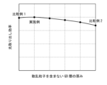
- FIG. 3 is a characteristic diagram showing simulation results of the relationship between the thickness of a QD layer that does not contain scattering particles and the light extraction efficiency in Example and Comparative Examples 1 and 2.
- FIG. 5 is a characteristic diagram showing simulation results of the relationship between the position in the wavelength conversion layer and the amount of excitation light absorbed per unit length in Example and Comparative Examples 1 and 2;
- FIG. 2 is a schematic cross-sectional view showing an example of a configuration of a light-emitting unit including a plurality of light-emitting devices shown in FIG.
- FIG. 1; 2 is a schematic cross-sectional view showing another example of the configuration of a light-emitting unit including a plurality of light-emitting devices shown in FIG. 1.
- FIG. It is a cross-sectional schematic diagram showing an example of a configuration of a light-emitting device according to Modification 1 of the present disclosure.
- FIG. 10 is a schematic cross-sectional view showing an example of a configuration of a light-emitting device according to Modification 2 of the present disclosure;
- FIG. 10 is a schematic cross-sectional view showing an example of a configuration of a light-emitting device according to Modification 3 of the present disclosure;
- FIG. 10 is a schematic cross-sectional view showing an example of a configuration of a light-emitting device according to Modification 4 of the present disclosure
- FIG. 11 is a schematic cross-sectional view showing an example of a configuration of a light-emitting device according to Modification 5 of the present disclosure
- FIG. 11 is a schematic cross-sectional view showing an example of a configuration of a light-emitting device according to Modification 6 of the present disclosure
- FIG. 12 is a schematic cross-sectional view showing an example of a configuration of a light-emitting device according to Modification 7 of the present disclosure
- FIG. 12 is a schematic cross-sectional view showing an example of a configuration of a light-emitting device according to Modification 8 of the present disclosure
- FIG. 21 is a schematic cross-sectional view showing an example of a configuration of a light-emitting unit according to Modification 9 of the present disclosure
- FIG. 20 is a schematic cross-sectional view showing an example of a configuration of a light-emitting unit according to Modification 10 of the present disclosure
- FIG. 21 is a schematic cross-sectional view showing an example of a configuration of a light-emitting unit according to Modification 11 of the present disclosure
- FIG. 12 is a cross-sectional schematic diagram showing an example of a cross-sectional configuration of a wavelength conversion layer according to Modification 12 of the present disclosure.
- FIG. 9 is a schematic cross-sectional view showing an example of a configuration of a light-emitting unit according to Modification 9 of the present disclosure
- FIG. 20 is a schematic cross-sectional view showing an example of a configuration of a light-emitting unit according to Modification 10 of the present disclosure
- FIG. 21 is a schematic cross-sectional view showing an example of a
- FIG. 21 is a schematic cross-sectional view showing an example of a configuration of a light-emitting device according to Modification 13 of the present disclosure
- 1 is a perspective view showing an example of a configuration of an image display device according to Application Example 1 of the present disclosure
- FIG. 21 is a schematic diagram showing an example of the layout of the image display device shown in FIG. 20
- FIG. It is a pixel circuit diagram of an active matrix drive system.
- FIG. 11 is a perspective view showing an example of a configuration of an image display device according to Application Example 2 of the present disclosure
- 24 is a perspective view showing the configuration of the mounting board shown in FIG. 23
- FIG. 25 is a perspective view showing the configuration of the unit board shown in FIG. 24;
- FIG. FIG. 11 is a diagram illustrating an example of an image display device according to Application Example 3 of the present disclosure;
- Embodiment (example of light-emitting device in which scattering particles are selectively dispersed on the light extraction surface side) 1-1. Configuration of Light Emitting Device 1-2. Configuration of Light Emitting Unit 1-3. Action and effect 2. Modified example 1 (an example in which the concentration of scattering particles is changed between the light source side and the light extraction surface side) 3.
- Modified example 2 (an example in which the concentration of the quantum dot phosphor is changed between the light source side and the light extraction surface side) 4.
- Modified example 3 (an example in which the configuration of the quantum dot phosphor is changed between the light source side and the light extraction surface side) 5.
- Modified example 4 (an example in which a resin layer is provided between the light source side and the light extraction surface side) 6.
- Modification 5 (an example in which a region containing only scattering particles is provided on the light source side) 7.
- Modification 6 (example using Cd-based quantum dot phosphor and Cd-free quantum dot phosphor) 8.
- Modified example 7 (an example in which the concentration of scattering particles in the in-plane direction is changed on the light extraction surface side) 9.
- Modification 8 (example in which the side surface of the wavelength conversion layer is inclined) 10.
- Modification 9 (Example of a light-emitting unit in which a microlens array is arranged on the light extraction surface) 11.
- Modification 10 (Another example of the configuration of the wavelength conversion layer of the blue light emitting device) 12.
- Modification 11 (Example of light-emitting unit in which color filters are arranged on the light extraction surface) 13.
- Modification 12 (another example of the structure of the wavelength conversion layer) 14.
- Modified Example 13 (example in which a textured structure is arranged on the light extraction surface) 15.
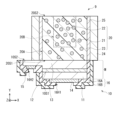
- FIG. 1 schematically illustrates an example of a cross-sectional configuration of a light-emitting device (light-emitting device 1) according to an embodiment of the present disclosure.
- the light-emitting device 1 is preferably used, for example, in the display pixels P of an image display device (eg, image display device 100, see FIG. 20).
- the light emitting device 1 of the present embodiment includes a light source unit 10 that emits excitation light EL, and a light emitting surface (surface 10S2) of the light source unit 10.
- the light emitting device 1 absorbs the excitation light EL and emits light of a different wavelength.
- a wavelength conversion layer 20 that The wavelength conversion layer 20 has, for example, a plurality of quantum dot phosphors 21 and a plurality of scattering particles 22 dispersed in a resin 23.
- the first region 20A and the second region are arranged in order from the surface 10S2 side of the light source unit 10. 20B.
- the first region 20A has a configuration in which only the plurality of quantum dot phosphors 21 are dispersed in the resin 23, and has a lower absorption coefficient of the excitation light EL than the second region 20B.
- the light source section 10 corresponds to a specific example of the "light source section" of the present disclosure.
- the light source unit 10 is a solid-state light-emitting device that emits light in a predetermined wavelength band from its upper surface (light-emitting surface), such as a light-emitting diode (LED) chip.
- LED light-emitting diode
- An LED chip refers to a chip cut out from a wafer used for crystal growth, not a package type covered with molded resin or the like.
- the LED chip has a size of, for example, 1 ⁇ m or more and 100 ⁇ m or less, and is called a micro LED.
- the light source section 10 has a first conductivity type layer 11, an active layer 12 and a second conductivity type layer 13 laminated in this order.
- the upper surface of the second conductivity type layer 13 is a light exit surface.
- the light source unit 10 has a columnar mesa portion M including a first conductivity type layer 11 and an active layer 12, and the first conductivity type layer 11 is exposed on the surface (surface 10S1) opposite to the light emitting surface. It has a step formed by a convex portion and a concave portion exposing the second conductivity type layer 13 .
- the surface opposite to the light extraction surface 10S2 (the surface 10S1 side) including the projections and recesses is the lower surface.
- the light source unit 10 further includes a first electrode 14 electrically connected to the first conductivity type layer 11 and a second electrode 15 electrically connected to the second conductivity type layer 13 .
- the first electrode 14 and the second electrode 15 are each provided on the surface 10S1 side.
- the first electrode 14 is arranged on the surface 10S1 of the first conductivity type layer, which is the convex portion on the lower surface
- the second electrode 15 is arranged on the surface 10S1 of the second conductivity type layer, which is the concave portion on the lower surface. are placed in
- the side surface of the light source section 10 made up of the first conductive layer 11, the active layer 12 and the second conductive layer 13 is covered with a laminated film 16 made up of an insulating film 16A and a reflective film 16B.
- the laminated film 16 extends, for example, to the periphery of the first electrode 14 and the second electrode 15, and has openings 16H1 and 16H2 on the first electrode 14 and the second electrode 15, respectively. That is, the first electrode and the second electrode are exposed to the outside through the openings 16H1 and 16H2, respectively.
- the materials forming the first conductivity type layer 11, the active layer 12 and the second conductivity type layer 13 are appropriately selected according to the desired wavelength band of light.
- the light source unit 10 may emit ultraviolet light having an emission wavelength of 360 nm or more and 430 nm or less, or blue band light having an emission wavelength of 430 nm or more and 500 nm or less (blue light ).
- Group III-V compound semiconductor materials include AlGaInN-based materials.
- a ZnSe-based material or a ZnO-based material may be used.
- the active layer 12 can be formed using, for example, a GaInN-based material.
- the light emitted from the light source unit 10 is not limited to ultraviolet light or blue light, and may be, for example, infrared light or red band light (red light).
- examples of III-V group compound semiconductor materials that emit infrared rays include AlGaInAs-based materials.
- III-V group compound semiconductor materials that emit red light include AlGaInP-based materials.
- the first electrode 14 is in contact with the first conductivity type layer 11 and is electrically connected to the first conductivity type layer 11 . That is, the first electrode 14 is in ohmic contact with the first conductivity type layer 11 .
- the first electrode 14 is, for example, a metal electrode, and is configured, for example, as a multilayer film (Ni/Au) of nickel (Ni) and gold (Au).
- the first electrode 14 may be made of a transparent conductive material such as indium tin oxide (ITO).
- the second electrode 15 is in contact with the second conductivity type layer 13 and is electrically connected to the second conductivity type layer 13 . That is, the second electrode 15 is in ohmic contact with the second conductivity type layer 13 .
- the second electrode 15 is, for example, a metal electrode, and is configured as, for example, a multilayer film (Ti/Al) of titanium (Ti) and aluminum (Al) or a multilayer film of chromium (Cr) and Au (Cr/Au). It is Alternatively, the second electrode 15 may be made of a transparent conductive material such as ITO.
- the laminated film 16 is formed from the side surface to the bottom surface of the light source section 10 as described above.
- the insulating film 16A and the reflective film 16B are thin films, respectively, and can be formed by thin film forming processes such as CVD, vapor deposition, and sputtering, for example.
- the insulating film 16A is for electrical insulation between the reflective film 16B and the first conductivity type layer 11, the active layer 12 and the second conductivity type layer 13. As shown in FIG.
- the insulating film 16A is preferably formed using a material transparent to light emitted from the active layer 12. As shown in FIG. Such materials include, for example, SiO 2 , Si 2 N 3 , Al 2 O 3 , TiO 2 and TiN.
- the thickness of the insulating film 16A is, for example, approximately 50 nm to 1 ⁇ m.
- the reflective film 16B is for reflecting the light emitted from the active layer 122.
- the reflective film 16B is provided with the insulating film 16A interposed therebetween.
- the reflective film 16B extends to the side surface and the lower surface of the light source unit 10, and is formed in the openings 16H1 and 16H2 of the insulating film 16A, for example, to a position slightly recessed from the end of the insulating film 16A.
- the reflective film 16B is insulated (electrically separated) from the first conductive layer 11, the active layer 12, the second conductive layer 13, the first electrode 14, and the second electrode 15 by the insulating film 16A.
- the reflective film 16B As a material for the reflective film 16B, it is preferable to use a material that reflects the light emitted from the active layer 12 to form it. Such materials include, for example, Ti, Al, silver (Ag), copper (Cu), Au, Ni, or alloys thereof.
- the thickness of the reflective film 16B is, for example, about 50 nm to 1 ⁇ m.
- An insulating film may be further formed on the reflective film 16B.
- the insulating film is preferably formed on the first electrode 14 and the second electrode 15 up to the insulating film 16A so as to cover the end portion of the reflective film 16B.
- the wavelength conversion layer 20 corresponds to a specific example of the "wavelength conversion layer" of the present disclosure.
- the wavelength conversion layer 20 is arranged on the surface 10S2 side of the light source unit 10, and converts the light emitted from the light source unit 10 into light of a desired wavelength band (eg, red light Lr, green light Lg, and blue light Lb). It is.
- the wavelength conversion layer 20 has a surface 20S1 and a surface 20S2 as a pair of surfaces facing each other.
- the surface 20S1 corresponds to the “first surface” of the present disclosure, and is arranged to face the surface 10S2 of the light source section 10 .
- the surface 20S2 corresponds to the “second surface” of the present disclosure, and serves as an extraction surface for wavelength-converted light.
- a plurality of quantum dot phosphors 21 and a plurality of scattering particles 22 are dispersed in the resin 23 as described above.
- the quantum dot phosphor 21 corresponds to a specific example of the "wavelength conversion material" of the present disclosure.
- the quantum dot phosphor 21 absorbs the light emitted from the light source section 10 as excitation light EL and emits fluorescence.
- the quantum dot phosphor 21 is, for example, a particulate phosphor that emits fluorescence in a blue wavelength band of 430 nm or more and 500 nm or less, a green wavelength band of 500 nm or more and 550 nm or less, or a red wavelength band of 610 nm or more and 780 nm or less. be.
- the quantum dot phosphor 21 can be selected from InP, GaInP, InAsP, CdSe, CdZnSe, CdTeSe, CdTe, or the like.
- the quantum dot phosphor 21 can be selected from, for example, InP, GaInP, ZnSeTe, ZnTe, CdSe, CdZnSe, CdS, CdSeS, and the like.
- the quantum dot phosphor 21 can be selected from ZnSe, ZnTe, ZnSeTe, CdSe, CdZnSe, CdS, CdZnS, CdSeS, and the like.
- the quantum dot phosphor 21 is not limited to the above, and for example, CuInSe 2 , CuInS 2 , CuInGaS, AgInS 2 or the like may be used.
- perovskite nanophosphors composed of CsPb(Cl/Br) 3 , CsPbBr 3 , CsPb(I/Br) 3 and CsPbI 3 may be used.
- the quantum dot phosphor 21 can also control the fluorescent color by its particle size. For example, the smaller the particle size, the shorter the fluorescence wavelength. In order to obtain fluorescence with high color purity, it is desirable to select a quantum dot phosphor whose particle size is controlled.
- the quantum dot phosphor 21 has an average particle size of, for example, 5 nm or more and 100 nm or less, and has a core/shell structure consisting of a core that emits light with an average particle size of about 2 nm to 10 nm, and a shell that covers and protects the core. .
- the shell consists of one layer or multiple layers.
- the shell may further be covered with an inorganic film such as silicon oxide ( SiO2 ) or aluminum oxide ( Al2O3 ).
- SiO2 silicon oxide
- Al2O3 aluminum oxide
- a large number of organic ligands are coordinated to the surface of the quantum dot phosphor 21, and the organic ligands cause aggregation of the quantum dot phosphor 21 when the quantum dot phosphor and the solvent are mixed. is suppressed and the dispersibility is improved.
- an inkjet or needle dispenser that ejects or applies the resin 23 mixed with the quantum dot phosphors 21 depending on the viscosity is used.
- This is classified as a plateless printing method, and in the above method, it is possible to selectively fill the quantum dot phosphor 21 only in the barrier, so the utilization efficiency of the quantum dot phosphor 21 can be improved.
- You may make it apply
- the quantum dot phosphor 21 may be applied to the entire base material by a spin coater, a PR method, or the like.
- an inorganic phosphor or an organic phosphor may be used as the wavelength conversion material.
- the scattering particles 22 scatter the excitation light EL emitted from the light source unit 10 and the fluorescence emitted from the quantum dot phosphor 21 to change the incident angle of the fluorescence to the light extraction surface 20S2, thereby improving the light extraction efficiency. It is for The scattering particles 22 are for increasing the effective optical path length of the excitation light EL, thereby improving the absorption rate of the excitation light EL. It is preferable that the scattering particles 22 have an average particle size larger than that of the quantum dot phosphor 21 and a refractive index larger than that of the resin 23 . For the scattering particles 22, it is preferable to use a dielectric substance having a particle size of, for example, 100 nm or more and 1000 nm or less.
- Specific materials of the scattering particles 22 include, for example, silicon oxide (SiO 2 ), titanium oxide (TiO 2 ), aluminum oxide (Al 2 O 3 ), aluminum nitride (AlN), boron nitride (BN) and zinc oxide. (ZnO) and the like.
- the scattering particles 22 may be, for example, air bubbles mixed in the filler 123 or aggregated quantum dot phosphors 21 .
- the resin 23 is for dispersing the quantum dot phosphors 21 and the scattering particles 22, and can be formed using, for example, a material having optical transparency to the excitation light EL.
- a specific material of the resin 23 for example, an ultraviolet curable resin or a thermosetting resin can be used.
- sol-gel glass or the like may be used.
- the resin 23 is not necessarily required, and the quantum dot phosphor 21 and the scattering particles 22 may be enclosed in the hollow structure.
- the wavelength conversion layer 20 has a first region 20A and a second region 20B that have different absorption coefficients for the excitation light EL in order from the surface 10S2 side of the light source section 10 .
- the first region 20 ⁇ /b>A does not include the plurality of scattering particles 22 in the resin 23 and has a configuration in which only the plurality of quantum dot phosphors 21 are dispersed.
- the second region 20 ⁇ /b>B has a configuration in which both the multiple quantum dot phosphors 21 and the multiple scattering particles 22 are dispersed in the resin 23 . Accordingly, the first region 20A has a lower absorption coefficient of the excitation light EL than the second region 20B.
- FIG. 2 shows simulation results of the relationship between the thickness of the QD layer (wavelength conversion layer 20) that does not contain the scattering particles 22 and the light extraction efficiency in Example and Comparative Examples 1 and 2.
- FIG. 3 shows simulation results of the relationship between the position in the wavelength conversion layer 20 and the amount of excitation light absorbed per unit length in Example and Comparative Examples 1 and 2.
- An example is a light-emitting device 1 having the above configuration.
- Comparative Example 1 is a light-emitting device in which a plurality of quantum dot phosphors 21 and a plurality of scattering particles are dispersed substantially uniformly throughout the resin 23 forming the wavelength conversion layer 20 .
- Comparative Example 2 is a light-emitting device in which only the plurality of quantum dot phosphors 21 are substantially uniformly dispersed throughout the resin 23 forming the wavelength conversion layer 20 without including the plurality of scattering particles 22 .
- the excitation light EL incident on the wavelength conversion layer 20 is scattered by the scattering particles 22 to increase the optical path length.
- the wavelength conversion layer 20 Example and Comparative Example 2 in which the plurality of scattering particles 22 are dispersed together with the plurality of quantum dot phosphors 21 does not contain the plurality of scattering particles 22 (Comparative Example 2).
- the absorption rate of the excitation light EL in the wavelength conversion layer 20 increases.
- the fluorescence emitted from the quantum dot phosphor 21 is scattered by the scattering particles 22, thereby improving the light extraction efficiency (FIG. 2).
- the temperature of the wavelength conversion layer 20 rises due to the heat generated by the quantum dot phosphors 21 due to the absorption of the excitation light EL. deterioration is more likely to occur.
- the heat generation of the quantum dot phosphor 21 due to the absorption of the excitation light EL becomes remarkable in the vicinity of the light source section 10 .
- the first region 20A in which only the plurality of quantum dot phosphors 21 are dispersed without including the plurality of scattering particles 22 in the resin 23 is provided on the light source unit 10 side.
- the light density in the vicinity of the light source section 10 side is reduced, and the absorption amount of the excitation light EL per unit length is reduced to approximately the same level as in Comparative Example 2 (FIG. 3). Therefore, temperature rise in the vicinity of the light source unit 10 is suppressed, and deterioration of the quantum dot phosphor 21 is reduced.
- a side surface (surface 20S3) of the wavelength conversion layer 20 is sealed by a side wall 24, for example.
- materials forming the sidewall 24 include SiO 2 , silicon (Si), resist, resin, and metal materials such as Cu and Al.
- a light reflecting film 25 may be formed between the wavelength conversion layer 20 and the sidewall 24 .
- the light reflecting film 25 is for reflecting the excitation light EL emitted from the light source unit 10 and scattered by the scattering particles 22 and fluorescence emitted from the quantum dot phosphor 21 into the wavelength conversion layer 20.
- the light reflecting film 25 is preferably formed using a material that has a high reflectance with respect to the excitation light EL and fluorescence regardless of the light incident angle. Examples of materials for the light reflecting film 25 include metal materials such as gold (Au), Ag , aluminum (Al ) and platinum (Pt ) ; A dielectric multilayer film in which 2 O 3 is combined is exemplified.
- FIG. 4 schematically shows a cross-sectional configuration of the light emitting unit 2. As shown in FIG.
- the light-emitting unit 2 is, for example, a plurality of light-emitting devices 1 arranged in a row.
- the light emitting unit 2 has, for example, an elongated shape extending in the arrangement direction of the plurality of light emitting devices 1 .
- the display pixels P of the image display device 100 include, for example, three color pixels Pr, Pg, and Pb corresponding to RGB, and the color pixels Pr, Pg, and Pb respectively emit light in corresponding wavelength bands.
- a light emitting device 1 is provided.
- FIG. 4 schematically shows an example of the cross-sectional configuration of the light emitting unit 2. As shown in FIG.
- the light-emitting unit 2 is composed of light-emitting devices 1R, 1G, and 1B that emit light corresponding to respective color pixels Pr, Pg, and Pb.
- the color pixel Pr has a light emitting device 1R that emits light in the red band (red light Lr)
- the color pixel Pg has a light emitting device 1G that emits light in the green band (green light Lg)
- the color pixel Pb has a light emitting device 1G that emits light in the green band (green light Lg).
- a light-emitting device 1B that emits light in the band (blue light Lb) is provided.
- the light-emitting unit 2 has an elongated shape extending in the arrangement direction of the light-emitting devices 1, the light-emitting device 1R is arranged, for example, near the short side of the light-emitting unit 2, and the light-emitting device 1B is arranged, for example, , near a short side of the light emitting unit 2 that is different from the adjacent short side of the light emitting device 1B.
- the light emitting device 1G is arranged, for example, between the light emitting device 1R and the light emitting device 1B.
- the positions of the light emitting devices 1R, 1G, and 1B are not limited to the above.
- the light emitting devices 1R, 1G and 1B are mounted on the driving substrate 41 via pad electrodes 42 and 43 and bumps 44 and 45, respectively. It should be noted that other bonding methods such as Cu—Cu bonding may be used for mounting on the drive substrate 41 .
- Each of the light emitting devices 1R, 1G, and 1B includes, for example, a plurality of quantum dot phosphors 21 for wavelength-converting the excitation light EL into light in a predetermined wavelength band on the light source unit 10 that emits blue light as the excitation light EL.
- a conversion layer 20 is arranged.
- a plurality of quantum dot phosphors 21 that emit red fluorescence and a plurality of scattering particles 22 are dispersed in the resin 23, and the excitation emitted from the light source unit 10
- the light EL is converted into red light by the quantum dot phosphor 21 and scattered by the scattering particles 22 to be taken out as red light Lr.
- a plurality of quantum dot phosphors 21 emitting green fluorescence and a plurality of scattering particles 22 are dispersed in a resin 23, and the excitation light EL emitted from the light source unit 10 is converted into green light by the quantum dot phosphor 21 and scattered by the scattering particles 22 to be taken out as green light Lg.
- the wavelength conversion layer 20 arranged in the light emitting device 1B for example, only the scattering particles 22 are dispersed in the resin 23, and the excitation light EL emitted from the light source section 10 is scattered by the scattering particles 22 and becomes blue light. Taken out as Lb.
- an excitation light reflection film 31 may be provided as a wavelength selection layer for selectively reflecting the excitation light EL on the wavelength conversion layer 20 of the light emitting devices 1R and 1G.
- the excitation light EL emitted from the light extraction surface 20S2 of the wavelength conversion layer 20 is reduced, and the color gamut can be improved.
- the contrast of external light can be improved.
- a yellow filter that selectively absorbs blue light may be arranged.
- the excitation light EL When the light source unit 10 that emits ultraviolet rays is used as the excitation light EL, for example, as shown in FIG. A wavelength conversion layer 20 in which a quantum dot phosphor 21 and a plurality of scattering particles 22 are dispersed in a resin 23 is arranged. As a result, the excitation light EL emitted from the light source section 10 in the light emitting device 1B is converted into blue light by the quantum dot phosphor 21 and scattered by the scattering particles 22 to be extracted as blue light Lb.
- the excitation light reflection film 31 is also arranged on the light emitting device 1B.
- the wavelength conversion layer 20 has the first region 20A and the second region 20B from the light source section 10 side, and the first region 20A contains only the plurality of quantum dot phosphors 21 in the resin 23. Both the plurality of quantum dot phosphors 21 and the plurality of scattering particles 22 are dispersed in the resin 23 in the second region 20B, and the first region 20A has a lower absorption of the excitation light EL than the second region 20B. coefficient. This reduces the absorption rate of the excitation light EL in the vicinity of the light source unit 10 . This will be explained below.
- a display device for augmented reality (AR) applications has been developed that combines a blue LED array with a color conversion layer using quantum dots (QDs).
- QDs quantum dots
- a QD layer with high color conversion efficiency is required in order to increase luminance and reduce power consumption.
- the color conversion efficiency of the QD layer in addition to the quantum yield of the QD, the light extraction efficiency from the QD layer is also important. For example, since the fluorescence emitted from the QDs emits isotropic light, the total reflection of the high-angle component at the interface between the QDs and the air reduces the amount of fluorescence extracted into the air.
- a method of adding scatterers to the QD layer is used.
- the addition of the scatterer also increases the optical path length of the excitation light in the QD layer, thereby providing the advantage of increasing the absorption rate of the excitation light. Accordingly, by adding a scatterer to the QD layer, the color conversion efficiency of the QD layer can be improved.
- the region of the QD layer near the LED has the highest light density and the highest temperature, resulting in greater degradation of the QDs. Since the excitation light absorptance in the vicinity of the LED becomes higher in the presence of the scatterer, the temperature of the QD layer in the vicinity of the LED becomes higher and the reliability deteriorates.
- the attained luminance of a light-emitting element using a color conversion layer of QDs is often rate-determined by reliability. For this reason, in order to improve the luminance of a light-emitting device, it becomes a challenge to achieve both light extraction efficiency and reliability of the device structure.
- an LED device has been proposed in which a layer (scatterer layer) to which only scatterers are added is added between the LED and the QD layer to which scatterers are added.
- the scatterer between the LED and the QD layer makes the excitation light uniform in the lateral direction, and the distance between the LED and the QD layer increases the area of the excitation light, thereby improving reliability.
- the scatterer layer causes the excitation light to return from the LED to the inside of the LED, thereby reducing the amount of light incident on the QD layer, thereby reducing the light extraction efficiency of the combined LED and color conversion layer.
- the angle of the QD sidewalls becomes vertical, which limits the effect of reducing the light density by increasing the distance between the LED and the QD.
- the first region 20A is provided by dispersing only the plurality of quantum dot phosphors 21 in the resin 23 on the light source section 10 side, and the resin 23 is provided on the light extraction surface 20S2 side.
- a second region 20B is provided in which both the plurality of quantum dot phosphors 21 and the plurality of scattering particles 22 are dispersed.
- the light-emitting device 1 of the present embodiment it is possible to achieve both an improvement in light extraction efficiency and an improvement in reliability.
- FIG. 6 schematically illustrates an example of a cross-sectional configuration of a light-emitting device (light-emitting device 3) according to Modification 1 of the present disclosure.
- This light-emitting device 3 like the light-emitting device 1 in the above-described embodiment, is suitably used for, for example, the display pixels P of an image display device (for example, the image display device 100).
- only the plurality of quantum dot phosphors 21 are dispersed in the resin 23 in the first region 20A on the light source unit 10 side, and the absorption coefficient of the excitation light EL in the vicinity of the light source unit 10 is changed to the excitation light EL in the vicinity of the light extraction surface 20S2.
- An example in which the absorption coefficient is lower than the absorption coefficient of the optical EL is shown, but the present invention is not limited to this.
- a plurality of scattering particles 22 may be dispersed in the first region 20A at a concentration lower than the concentration of the plurality of scattering particles in the second region 20B.
- both the plurality of quantum dot phosphors 21 and the plurality of scattering particles 22 are dispersed in the first region 20A, and the concentration of the plurality of scattering particles in the first region 20A is It was made lower than the concentration of a plurality of scattering particles. This makes it possible to obtain the same effects as those of the above-described embodiment.
- FIG. 7 schematically illustrates an example of a cross-sectional configuration of a light-emitting device (light-emitting device 4) according to Modification 2 of the present disclosure.
- the light-emitting device 4 like the light-emitting device 1 in the above-described embodiment, is suitably used for, for example, the display pixels P of an image display device (for example, the image display device 100).
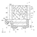
- the concentration of the plurality of quantum dot phosphors 21 dispersed in the first region 20A may be made lower than the concentration of the plurality of quantum dot phosphors 21 dispersed in the second region 20B.
- the concentration of the plurality of quantum dot phosphors 21 in the first region 20A is made lower than the concentration of the plurality of scattering particles in the second region 20B.
- the amount of heat generated in the first region 20A is further reduced compared to the above-described embodiment, and the reliability can be further improved. Further, compared to the above embodiment, higher luminance can be achieved.
- FIG. 8 schematically illustrates an example of a cross-sectional configuration of a light-emitting device (light-emitting device 5) according to Modification 3 of the present disclosure.
- This light-emitting device 5 like the light-emitting device 1 in the above-described embodiment, is suitably used for, for example, the display pixels P of an image display device (for example, the image display device 100).
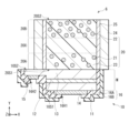
- a plurality of quantum dot phosphors 26 having a different material, composition, or core/shell structure from the plurality of quantum dot phosphors 21 dispersed in the second region 20B may be dispersed in the first region 20A.
- quantum dot phosphors 26 having a lower absorption coefficient of the excitation light EL than the quantum dot phosphors 21 dispersed in the second region 20B are dispersed.
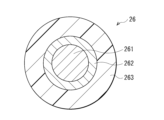
- FIG. 9 schematically shows the cross-sectional configuration of the quantum dot phosphor 26.
- the absorption coefficient of the quantum dot phosphor 26 can be controlled by, for example, changing the thickness ratio of the core 261 and the shell A 262 and shell B 263 covering the core 261 .
- the quantum dot phosphors 26 having a lower absorption coefficient of the excitation light EL than the quantum dot phosphors 21 dispersed in the second region 20B are dispersed in the first region 20A.
- the amount of heat generated in the first region 20A is further reduced compared to the above-described embodiment, and the reliability can be further improved. Further, compared to the above embodiment, higher luminance can be achieved.
- FIG. 10 schematically illustrates an example of a cross-sectional configuration of a light-emitting device (light-emitting device 6) according to Modification 4 of the present disclosure.
- This light-emitting device 6 like the light-emitting device 1 in the above-described embodiment, is suitably used for, for example, the display pixels P of an image display device (for example, the image display device 100).
- the plurality of quantum dot phosphors 21 are dispersed in the resin 23 in the first region 20A on the light source unit 10 side, and the absorption coefficient of the excitation light EL in the vicinity of the light source unit 10 is changed to the excitation light EL in the vicinity of the light extraction surface 20S2.
- An example in which the absorption coefficient is lower than the absorption coefficient of the optical EL is shown, but the present invention is not limited to this.
- a region 20X made only of the resin 23 may be provided between the first region 20A in which only the plurality of quantum dot phosphors 21 are dispersed in the resin 23 and the second region 20B in which both the plurality of quantum dot phosphors 21 and the plurality of scattering particles 22 are dispersed .
- the region 20X made only of the resin 23 is provided between the first region 20A and the second region 20B so as to spatially separate the first region 20A and the second region 20B. made it As a result, it is possible to reduce the influence of heat generation on the first region 20A with respect to the second region 20B. Therefore, the reliability can be further improved as compared with the above embodiment. Further, compared to the above embodiment, higher luminance can be achieved.
- FIG. 11 schematically illustrates an example of a cross-sectional configuration of a light-emitting device (light-emitting device 7) according to Modification 5 of the present disclosure.
- This light-emitting device 7 is suitably used for, for example, the display pixels P of an image display device (for example, the image display device 100), like the light-emitting device 1 in the above embodiment.
- the first region 20A in which only the plurality of quantum dot phosphors 21 are dispersed in the resin 23 and the second region 20B in which both the plurality of quantum dot phosphors 21 and the plurality of scattering particles 22 are dispersed are provided in this order from the light source unit 10 side, but the configuration of the wavelength conversion layer 20 is not limited to this.
- the wavelength conversion layer 20 is divided into, for example, three regions, a first region 20A, a second region 20B, and a third region 20C, from the light source unit 10 side, and the first region 20A contains only the plurality of scattering particles 22.
- the second region 20B and the third region 20C may have the same configurations as the first region 20A and the second region 20B of the above embodiment, respectively.
- the first region 20A, the second region 20B, and the third region 20C are divided from the light source unit 10 side, for example, into three regions, and only the plurality of scattering particles 22 are placed in the first region 20A. I tried to disperse it.
- the excitation light EL incident on the wavelength conversion layer 20 from the light source unit 10 is homogenized in the first region 20A, so that only the plurality of quantum dot phosphors 21 are incident on the second region 20B dispersed in the resin 23. In-plane uniformity of the excitation light EL can be improved. Therefore, the reliability can be further improved as compared with the above embodiment.
- FIG. 12 schematically illustrates an example of a cross-sectional configuration of a light-emitting device (light-emitting device 8) according to Modification 6 of the present disclosure.
- the light-emitting device 8 like the light-emitting device 1 in the above-described embodiment, is suitably used for, for example, the display pixels P of an image display device (for example, the image display device 100).
- the first region 20A in which only the plurality of quantum dot phosphors 21 are dispersed in the resin 23 and the second region 20B in which both the plurality of quantum dot phosphors 21 and the plurality of scattering particles 22 are dispersed are provided in this order from the light source unit 10 side, but the configuration of the wavelength conversion layer 20 is not limited to this.
- a third region 20C in which both the plurality of quantum dot phosphors 21B and the plurality of scattering particles 22 are dispersed may be further provided on the second region 20B of the above embodiment.
- the multiple quantum dot phosphors 21A dispersed in the first region 20A and the second region 20B are made of different materials from the multiple quantum dot phosphors 21B dispersed in the third region 20C.
- so-called Cd-based quantum dot phosphors have higher light resistance than Cd-free quantum dot phosphors.
- the Cd-based quantum dot phosphor is used for the first region 20A and the second region 20B, and the Cd-free quantum dot phosphor is used for the third region 20C.
- the first region 20A in which only the plurality of quantum dot phosphors 21 are dispersed in the resin 23 in the wavelength conversion layer 20 on the light source unit 10 side other regions (for example, the farthest from the light source unit 10) It becomes possible to use a Cd-free quantum dot phosphor for the third region 20C). Therefore, the Cd concentration in the wavelength conversion layer 20 can be reduced, and the environmental load can be reduced.
- FIG. 13 schematically illustrates an example of a cross-sectional configuration of a light-emitting device (light-emitting device 9) according to Modification 7 of the present disclosure.
- This light-emitting device 9 like the light-emitting device 1 in the above-described embodiment, is suitably used for, for example, the display pixels P of an image display device (for example, the image display device 100).
- the first region 20A in which only the plurality of quantum dot phosphors 21 are dispersed in the resin 23 and the second region 20B in which both the plurality of quantum dot phosphors 21 and the plurality of scattering particles 22 are dispersed are provided in this order from the light source unit 10 side, but the configuration of the wavelength conversion layer 20 is not limited to this.
- the first region 20A may extend toward the light extraction surface 20S2, and the first region 20A may be provided around the second region 20B.
- the concentration of the plurality of quantum dot phosphors 21 in the wavelength conversion layer 20 is also changed in the lateral direction.
- the light extraction efficiency is relatively high even near the center of the light emitting device 9 . Therefore, by combining with a microlens array 32 to be described later, it is possible to improve the controllability of the light distribution characteristics of the light emitting device 9 .
- FIG. 14 schematically illustrates an example of a cross-sectional configuration of a light-emitting device (light-emitting device 1) according to Modification 8 of the present disclosure.
- the side surface (surface 20S3) of wavelength conversion layer 20 is vertical is shown, but the present invention is not limited to this.
- the surface 20S3 of the wavelength conversion layer 20 may be an inclined surface extending from the surface 20S1 toward the surface 20S2. This makes it possible to further improve the light extraction efficiency of fluorescence emitted in the wavelength conversion layer 20 .
- FIG. 15 schematically illustrates an example of a cross-sectional configuration of a light-emitting unit (light-emitting unit 2A) according to Modification 9 of the present disclosure.
- a microlens array 32 may be provided on the light extraction surface 20S2 of the light emitting devices 1R, 1G, and 1B.
- the microlens array 32 corresponds to a specific example of the "light distribution control structure" of the present disclosure.
- a photonic crystal, a moth-eye structure, a nanoantenna, and a metamaterial may be provided. This makes it possible to increase the luminance on the low-angle side, for example.
- FIG. 16 schematically illustrates an example of a cross-sectional configuration of a light-emitting unit (light-emitting unit 2B) according to Modification 10 of the present disclosure.
- a plurality of scattering particles 22 are dispersed substantially uniformly in the wavelength conversion layer 20 arranged in the light emitting device 1B
- the present invention is not limited to this.
- the first region 20A and the second region 20B are provided, and the concentration of the plurality of scattering particles 22 in the second region 20B is higher than the concentration of the plurality of scattering particles 22 in the first region 20A. You can make it higher. This reduces the ratio of the excitation light EL returning to the light source unit 10 . Therefore, it is possible to improve the light extraction efficiency of the light emitting device 1B and reduce the power consumption.
- FIG. 17 schematically illustrates an example of a cross-sectional configuration of a light-emitting unit (light-emitting unit 2C) according to Modification 11 of the present disclosure.
- the corresponding red light Lr, green light Lg, and blue light Lb are emitted from the light emitting devices 1R, 1G, and 1B, but the present invention is not limited to this.
- white light is emitted from each wavelength conversion layer 20 of the light emitting devices 1R, 1G, and 1B, and corresponding color filters (red filters 33R , a green filter 33G and a blue filter 33B) may be provided. This eliminates the step of separately painting the wavelength conversion layer 20 for each of the color pixels Pr, Pg, and Pb, thus making it possible to reduce the manufacturing cost.
- FIG. 18 schematically illustrates another example of the cross-sectional configuration of the wavelength conversion layer 20 in Modification 12 of the present disclosure.
- the wavelength conversion layer 20 is made to emit white light Lw, and the top and bottom of the wavelength conversion layer 20 are sealed with, for example, barrier films 27 and 28 having light transmittance. It is good also as the wavelength conversion layer 20 of shape.
- Such a QD sheet can be used, for example, as a backlight for a liquid crystal display device.
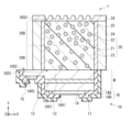
- FIG. 19 schematically illustrates an example of a cross-sectional configuration of a light-emitting device (light-emitting device 1) according to Modification 13 of the present disclosure.
- a texture structure 34 may be further provided on the light extraction surface (surface 20S2) of the wavelength conversion layer 20.
- FIG. 19 As a result, of the fluorescence emitted from the wavelength conversion layer 20, the fluorescence whose angle is smaller than the critical angle while the fluorescence with the critical angle or more is repeatedly reflected in the wavelength conversion layer 20 can be extracted from the light extraction surface. Become. Therefore, in addition to the effects of the above embodiments, it is possible to achieve high luminance.
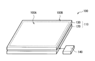
- FIG. 20 is a perspective view showing an example of a schematic configuration of an image display device (image display device 100).
- the image display device 100 is a so-called LED display, and the display pixels P use the light-emitting device (for example, the light-emitting device 1) of the present disclosure.
- the image display device 100 includes a display panel 110 and a control circuit 140 that controls driving of the display panel 110, as shown in FIG. 20, for example.
- the display panel 110 is obtained by superimposing a mounting substrate 120 and a counter substrate 130 on each other.
- the surface of the counter substrate 130 serves as an image display surface, and has a display area 100A in the central portion and a frame area 100B as a non-display area around it.
- FIG. 21 shows an example of the wiring layout of the area corresponding to the display area 100A on the surface of the mounting substrate 120 on the counter substrate 130 side.
- a region corresponding to the display region 100A on the surface of the mounting substrate 120 as shown in FIG. are placed.
- a plurality of scan wirings 1022 are formed extending in a direction intersecting (for example, perpendicular to) the data wirings 1021, and are arranged in parallel with a pitch of
- the data wiring 1021 and the scan wiring 1022 are made of a conductive material such as Cu, for example.
- the scan wiring 1022 is formed, for example, on the outermost layer, for example, on an insulating layer (not shown) formed on the base material surface.
- the base material of the mounting board 120 is made of, for example, a silicon substrate or a resin substrate, and the insulating layer on the base material is made of, for example, SiN, SiO, aluminum oxide (AlO), or a resin material.
- the data wiring 1021 is formed in a layer (for example, a layer below the outermost layer) different from the outermost layer including the scan wiring 1022, for example, formed in an insulating layer on the substrate. .
- black is provided as necessary.
- Black is for enhancing contrast and is composed of a light-absorbing material.
- the black is formed, for example, at least on areas where pad electrodes 1021B and 1022B, which will be described later, are not formed on the surface of the insulating layer. It should be noted that black can be omitted if necessary.
- Display pixels P are formed in the vicinity of the intersections of the data lines 1021 and the scan lines 1022, and a plurality of display pixels P are arranged, for example, in a matrix in the display area 100A.
- Each display pixel P is mounted with a light-emitting unit 2 including a plurality of light-emitting devices 1 corresponding to, for example, RGB.
- one display pixel P is composed of three light emitting devices 1R, 1G, and 1B, and red light is output from the light emitting device 1R, green light is output from the light emitting device 1G, and blue light is output from the light emitting device 1B. A case where it is possible to do so is exemplified.
- the image display device 100 shown in FIG. 20 is an example of a passive matrix image display device.
- the light emitting device 1 of the present embodiment can be applied not only to a passive matrix image display device (image display device 100), but also to an active matrix image display device. Note that the active matrix image display device does not require the frame region 100B shown in FIG. 20, for example.
- the passive matrix drive system In the passive matrix drive system, increasing the number of scan wires shortens the time allocated to each light emitting device, so the injection current must be increased as the duty ratio decreases, resulting in a decrease in luminous efficiency and device life. There is fear. To avoid this, it is necessary to lower the maximum brightness setting value.
- the screen is divided into multiple partial screens and passive matrix drive is used in parallel. , or a method of actively driving the light emitting device is adopted.
- Parallel passive matrix driving requires wiring to be pulled out to the back of each partial screen to connect the drive circuit, and the image signal must also be divided and parallelized according to each partial screen.
- a signal voltage holding and voltage-current conversion circuit is provided for each pixel, so that the above-described screen division is not performed, or at least in a state where the number of divisions is small, and higher luminance than passive matrix driving is obtained. be able to.
- FIG. 22 shows an example of a general active matrix driven pixel circuit.
- a switching transistor (Tr1), a driving transistor (Tr2), and a capacitive element (Cs) are provided for each display pixel P (light emitting devices 1R, 1G, 1B, near intersections between data wiring 1021 and scanning wiring 1022). are provided respectively.
- a switching transistor is used as a switch to write Vsig to a capacitive element, and in addition, the driving transistor is used as a current source for current control by the potential difference of power supply (Vcc)-Vsig to current-modulate the light-emitting device.
- the light emitting unit 2 is provided with a pair of terminal electrodes for each of the light emitting devices 1R, 1G, and 1B, for example.
- One terminal electrode is electrically connected to, for example, the data wiring 1021 and is electrically connected to the other terminal electrode, for example, the scan wiring 1022 .
- the terminal electrode is electrically connected to the pad electrode 1021B at the tip of the branch 1021A provided on the data line 1021.
- the terminal electrode is electrically connected to the pad electrode 1022B at the tip of the branch 1022A provided in the scan wiring 1022.
- the pad electrodes 1021B and 1022B are formed, for example, on the outermost layer, and are provided at the site where the light emitting unit 2 is mounted, for example, as shown in FIG.
- the pad electrodes 121B and 122B are made of a conductive material such as Au (gold).
- the mounting substrate 120 is further provided with, for example, a plurality of pillars (not shown) that regulate the distance between the mounting substrate 120 and the opposing substrate 130 .
- the struts may be provided in a region facing the display region 100A, or may be provided in a region facing the frame region 100B.
- the counter substrate 130 is made of, for example, a glass substrate or a resin substrate.
- the surface on the side of the light emitting device 1 may be flat, but is preferably rough.
- the rough surface may be provided over the entire region facing the display region 100A, or may be provided only in the region facing the display pixels P.
- the rough surface has fine unevenness on which light emitted from the display pixels P enters.
- the unevenness of the rough surface can be produced by sandblasting, dry etching, or the like, for example.
- the control circuit 140 drives each display pixel P (each light emitting unit 2) based on the video signal.
- the control circuit 140 includes, for example, a data driver that drives the data lines 1021 connected to the display pixels P and a scan driver that drives the scan lines 1022 connected to the display pixels P.
- FIG. 20 the control circuit 140 may be provided separately from the display panel 110 and connected to the mounting substrate 120 via wiring, or may be mounted on the mounting substrate 120.
- FIG. 23 is a perspective view showing another configuration example (image display device 200) of an image display device using the light emitting device (for example, light emitting device 1) of the present disclosure.
- the image display device 200 is a so-called tiling display.
- the image display device 200 includes, for example, a display panel 210 and a control circuit 240 that controls driving of the display panel 210, as shown in FIG.
- the display panel 210 is obtained by superimposing a mounting substrate 220 and a counter substrate 230 on each other.
- the surface of the counter substrate 230 serves as an image display surface, and has a display area in the central portion and a frame area as a non-display area around it (both not shown).
- the counter substrate 230 is arranged, for example, at a position facing the mounting substrate 220 with a predetermined gap therebetween. Note that the counter substrate 230 may be in contact with the top surface of the mounting substrate 220 .
- FIG. 24 schematically shows an example of the configuration of the mounting substrate 220.
- the mounting board 220 is composed of a plurality of unit boards 250 laid out like tiles. Note that FIG. 24 shows an example in which the mounting substrate 220 is configured by nine unit substrates 250, but the number of unit substrates 250 may be ten or more, or may be eight or less.
- the unit substrate 250 has, for example, a plurality of light emitting devices 1 laid out like tiles and a supporting substrate 260 supporting each light emitting device 1 .
- Each unit board 250 further has a control board (not shown).
- the support substrate 260 is composed of, for example, a metal frame (metal plate) or a wiring board. When the support substrate 260 is configured by a wiring substrate, it can also serve as a control substrate. At this time, at least one of the support substrate 260 and the control substrate is electrically connected to each light emitting device 1 .
- FIG. 26 shows the appearance of the transparent display 300.
- the transparent display 300 has, for example, a display section 310 , an operation section 311 and a housing 312 .
- the display unit 310 uses the light-emitting device of the present disclosure (for example, the light-emitting device 1).
- the transparent display 300 can display images and character information while the background of the display section 310 is transparent.
- a light-transmitting substrate is used as a mounting substrate.
- Each electrode provided in the light-emitting device 1 is formed using a conductive material having optical transparency, like the mounting substrate.
- each electrode has a structure that is difficult to see by narrowing the width of the wiring or thinning the thickness of the wiring.
- the transparent display 300 can perform black display by superimposing a liquid crystal layer having a driving circuit, for example, and can switch between transmission and black display by controlling the light distribution direction of the liquid crystal.
- the present invention is not limited to this.
- the light source unit 10 for example, an LED (OLED) using an organic semiconductor or a semiconductor laser (Laser Diode: LD) can be used.
- the light-emitting device for example, the light-emitting device 1 shown in the above embodiments and the like can be used in smartphones, televisions, notebook PCs, AR/VR equipment, projectors, head-up displays, in addition to the application examples 1 to 3 described above. (HUD), smart watches and video walls, etc.
- HUD head-up displays
- the present disclosure can also be configured as follows.
- a plurality of wavelength conversion materials and a plurality of scattering particles for converting first light emitted from the light source unit into second light having different wavelength bands are added to the wavelength conversion layer in the light source unit.
- the absorption coefficient of the first light in the vicinity of the side surface (first surface) is made lower than the absorption coefficient of the first light in the vicinity of the light extraction surface (second surface). This reduces the absorptance of the excitation light in the vicinity of the light source. Therefore, it is possible to achieve both light extraction efficiency and reliability.
- a light source unit having a light exit surface and emitting first light from the light exit surface;
- the light source unit has a first surface arranged on the light emitting surface side of the light source unit and arranged to face the light emitting surface and a second surface opposite to the first surface, and the first surface
- a light emitting device comprising: a wavelength converting layer having a lower absorption coefficient for said first light in its vicinity.
- the wavelength conversion layer has a first region and a second region in order from the first surface side, The light-emitting device according to (1), wherein the concentration of the plurality of scattering particles in the first region is lower than the concentration of the plurality of scattering particles in the second region. (3) The light-emitting device according to (2), wherein the first region does not include the plurality of scattering particles. (4) The wavelength conversion layer has a first region and a second region in order from the first surface side, any one of (1) to (3), wherein the concentration of the plurality of wavelength conversion materials in the first region is lower than the concentration of the plurality of wavelength conversion materials in the second region; A light emitting device as described.
- the wavelength conversion layer has a first region, a second region and a third region in order from the first surface side, the first region does not contain the plurality of wavelength converting materials and contains only the plurality of scattering particles; the second region does not contain the plurality of scattering particles and contains only the plurality of wavelength converting materials;
- the light emitting device according to any one of (1) to (6), wherein the third region comprises the plurality of wavelength converting materials and the plurality of scattering particles.
- the wavelength conversion layer has a first region, a second region and a third region in order from the first surface side, the first region does not include the plurality of scattering particles and only includes a plurality of first wavelength converting materials; said second region comprises said plurality of first wavelength converting materials and said plurality of scattering particles; said third region comprises a plurality of second wavelength converting materials and said plurality of scattering particles;
- the light emitting device according to any one of (1) to (6), wherein the first wavelength converting material has higher light resistance than the second wavelength converting material.
- the light-emitting device wherein the first wavelength conversion material is a cadmium-based quantum dot phosphor, and the second wavelength conversion material is a cadmium-free quantum dot phosphor.
- the wavelength conversion layer has a first region and a second region in order from the first surface side, The plurality of quantum dots contained in the first region and the second region are different from each other in material, composition, and core/shell structure. Any one of (1) to (9) above. luminous device.
- the first wavelength conversion layer converts the first light into red light
- the second wavelength conversion layer converts the first light into green light
- the light-emitting device according to any one of (1) to (13), wherein the third wavelength conversion layer transmits or converts the first light into blue light.
- the light emission according to (14) above further comprising a wavelength selective layer that selectively reflects the first light on at least the second surfaces of the first wavelength conversion layer and the second wavelength conversion layer.
- the light distribution control structure is any one of a microlens array, a photonic crystal, a moth-eye structure, a nanoantenna, and a metamaterial.
- the wavelength conversion layer a first wavelength conversion layer arranged on the light exit surface side of the first light source section, and a second wavelength conversion layer arranged on the light exit surface side of the second light source section.
- the first wavelength conversion layer, the second wavelength conversion layer and the third wavelength conversion layer each convert the first light into white light, a red filter that selectively transmits red light on the second surface of the first wavelength conversion layer; a green filter that selectively transmits green light on the second surface of the second wavelength conversion layer;
- the light emitting device is a light source unit having a light exit surface and emitting first light from the light exit surface;
- the light source unit has a first surface arranged on the light emitting surface side of the light source unit and arranged to face the light emitting surface and a second surface opposite to the first surface, and the first surface
- a wavelength conversion layer having a lower absorption coefficient than the first light in the vicinity thereof.
Landscapes
- Physics & Mathematics (AREA)
- General Physics & Mathematics (AREA)
- Chemical & Material Sciences (AREA)
- Dispersion Chemistry (AREA)
- Optics & Photonics (AREA)
- Engineering & Computer Science (AREA)
- Theoretical Computer Science (AREA)
- Led Device Packages (AREA)
Priority Applications (3)
| Application Number | Priority Date | Filing Date | Title |
|---|---|---|---|
| JP2023559508A JPWO2023085010A1 (https=) | 2021-11-12 | 2022-10-18 | |
| US18/707,097 US20250031496A1 (en) | 2021-11-12 | 2022-10-18 | Light emission device and image display apparatus |
| CN202280073689.3A CN118202478A (zh) | 2021-11-12 | 2022-10-18 | 发光器件和图像显示装置 |
Applications Claiming Priority (2)
| Application Number | Priority Date | Filing Date | Title |
|---|---|---|---|
| JP2021185012 | 2021-11-12 | ||
| JP2021-185012 | 2021-11-12 |
Publications (1)
| Publication Number | Publication Date |
|---|---|
| WO2023085010A1 true WO2023085010A1 (ja) | 2023-05-19 |
Family
ID=86335640
Family Applications (1)
| Application Number | Title | Priority Date | Filing Date |
|---|---|---|---|
| PCT/JP2022/038786 Ceased WO2023085010A1 (ja) | 2021-11-12 | 2022-10-18 | 発光デバイスおよび画像表示装置 |
Country Status (4)
| Country | Link |
|---|---|
| US (1) | US20250031496A1 (https=) |
| JP (1) | JPWO2023085010A1 (https=) |
| CN (1) | CN118202478A (https=) |
| WO (1) | WO2023085010A1 (https=) |
Cited By (2)
| Publication number | Priority date | Publication date | Assignee | Title |
|---|---|---|---|---|
| WO2025134400A1 (ja) * | 2022-12-22 | 2025-06-26 | スタンレー電気株式会社 | 発光装置 |
| WO2025192031A1 (ja) * | 2024-03-12 | 2025-09-18 | ソニーセミコンダクタソリューションズ株式会社 | 発光装置および画像表示装置 |
Citations (10)
| Publication number | Priority date | Publication date | Assignee | Title |
|---|---|---|---|---|
| JP2006313902A (ja) * | 2005-05-02 | 2006-11-16 | Samsung Electro Mech Co Ltd | 白色発光素子 |
| JP2014170938A (ja) * | 2013-03-04 | 2014-09-18 | Osram Sylvania Inc | 量子ドット層を有する赤色ランプ |
| JP2016111292A (ja) * | 2014-12-10 | 2016-06-20 | 富士フイルム株式会社 | 波長変換部材、バックライトユニット、液晶表示装置、および波長変換部材の製造方法 |
| JP2016162850A (ja) * | 2015-02-27 | 2016-09-05 | 豊田合成株式会社 | 発光装置 |
| JP2016186875A (ja) * | 2015-03-27 | 2016-10-27 | 住友化学株式会社 | 発光素子 |
| US20180351052A1 (en) * | 2017-06-05 | 2018-12-06 | Samsung Electronics Co., Ltd. | Quantum dot glass cell and light-emitting device package including the same |
| JP2019061230A (ja) * | 2017-09-08 | 2019-04-18 | マブン オプトロニックス カンパニー リミテッドMaven Optronics Co., Ltd. | 量子ドットに基づいて色変換する発光装置、および、その製造方法 |
| US20200388732A1 (en) * | 2017-12-14 | 2020-12-10 | Osram Oled Gmbh | Luminophore mixture, conversion element and optoelectronic component |
| CN112103380A (zh) * | 2020-06-24 | 2020-12-18 | 佛山市国星光电股份有限公司 | 一种量子点发光器件及其制造方法 |
| WO2021166785A1 (ja) * | 2020-02-19 | 2021-08-26 | ソニーグループ株式会社 | 発光素子、発光素子アレイ及び表示装置 |
-
2022
- 2022-10-18 JP JP2023559508A patent/JPWO2023085010A1/ja active Pending
- 2022-10-18 WO PCT/JP2022/038786 patent/WO2023085010A1/ja not_active Ceased
- 2022-10-18 US US18/707,097 patent/US20250031496A1/en active Pending
- 2022-10-18 CN CN202280073689.3A patent/CN118202478A/zh active Pending
Patent Citations (10)
| Publication number | Priority date | Publication date | Assignee | Title |
|---|---|---|---|---|
| JP2006313902A (ja) * | 2005-05-02 | 2006-11-16 | Samsung Electro Mech Co Ltd | 白色発光素子 |
| JP2014170938A (ja) * | 2013-03-04 | 2014-09-18 | Osram Sylvania Inc | 量子ドット層を有する赤色ランプ |
| JP2016111292A (ja) * | 2014-12-10 | 2016-06-20 | 富士フイルム株式会社 | 波長変換部材、バックライトユニット、液晶表示装置、および波長変換部材の製造方法 |
| JP2016162850A (ja) * | 2015-02-27 | 2016-09-05 | 豊田合成株式会社 | 発光装置 |
| JP2016186875A (ja) * | 2015-03-27 | 2016-10-27 | 住友化学株式会社 | 発光素子 |
| US20180351052A1 (en) * | 2017-06-05 | 2018-12-06 | Samsung Electronics Co., Ltd. | Quantum dot glass cell and light-emitting device package including the same |
| JP2019061230A (ja) * | 2017-09-08 | 2019-04-18 | マブン オプトロニックス カンパニー リミテッドMaven Optronics Co., Ltd. | 量子ドットに基づいて色変換する発光装置、および、その製造方法 |
| US20200388732A1 (en) * | 2017-12-14 | 2020-12-10 | Osram Oled Gmbh | Luminophore mixture, conversion element and optoelectronic component |
| WO2021166785A1 (ja) * | 2020-02-19 | 2021-08-26 | ソニーグループ株式会社 | 発光素子、発光素子アレイ及び表示装置 |
| CN112103380A (zh) * | 2020-06-24 | 2020-12-18 | 佛山市国星光电股份有限公司 | 一种量子点发光器件及其制造方法 |
Cited By (2)
| Publication number | Priority date | Publication date | Assignee | Title |
|---|---|---|---|---|
| WO2025134400A1 (ja) * | 2022-12-22 | 2025-06-26 | スタンレー電気株式会社 | 発光装置 |
| WO2025192031A1 (ja) * | 2024-03-12 | 2025-09-18 | ソニーセミコンダクタソリューションズ株式会社 | 発光装置および画像表示装置 |
Also Published As
| Publication number | Publication date |
|---|---|
| CN118202478A (zh) | 2024-06-14 |
| JPWO2023085010A1 (https=) | 2023-05-19 |
| US20250031496A1 (en) | 2025-01-23 |
Similar Documents
| Publication | Publication Date | Title |
|---|---|---|
| JP7392653B2 (ja) | 発光デバイスおよび画像表示装置 | |
| JP7484727B2 (ja) | 発光デバイスおよび画像表示装置 | |
| CN110858599B (zh) | 像素阵列封装结构及显示面板 | |
| KR102377794B1 (ko) | 반도체 발광 소자를 이용한 디스플레이 장치 및 이의 제조방법 | |
| CN107211504B (zh) | 使用半导体发光器件的显示装置及制造方法 | |
| EP3076442B1 (en) | Display device using semiconductor light emitting device | |
| US10833229B2 (en) | Display device using semiconductor light emitting element and method for manufacturing same | |
| CN109792817B (zh) | 使用半导体发光器件的显示装置及其制造方法 | |
| CN110050511A (zh) | 使用半导体发光二极管的显示装置 | |
| US12154936B2 (en) | Display module and manufacturing method thereof | |
| CN110050512B (zh) | 使用半导体发光元件的显示装置 | |
| JP7666496B2 (ja) | 発光デバイス、および発光デバイスの製造方法 | |
| JP7772785B2 (ja) | 発光装置および画像表示装置 | |
| WO2023085010A1 (ja) | 発光デバイスおよび画像表示装置 | |
| CN113346002B (zh) | 显示面板 | |
| WO2022014421A1 (ja) | 発光装置および画像表示装置 | |
| KR20180038272A (ko) | 반도체 발광소자를 이용한 디스플레이 장치 및 이의 제조방법 | |
| KR20220111804A (ko) | 디스플레이 모듈 및 그 제조 방법 | |
| WO2023176539A1 (ja) | 発光装置および発光装置の製造方法ならびに画像表示装置 | |
| CN119563396A (zh) | 包括形成在自发光器件上的颜色转换层的显示模块及其制造方法 | |
| CN111863864B (zh) | 显示面板 | |
| KR20200005096A (ko) | 반도체 발광 소자를 이용한 디스플레이 장치 및 이의 제조방법 | |
| CN115498091A (zh) | 微型发光二极管显示面板 | |
| CN117858534A (zh) | 显示面板及其制备方法、显示装置 | |
| CN214476125U (zh) | 显示面板和显示装置 |
Legal Events
| Date | Code | Title | Description |
|---|---|---|---|
| 121 | Ep: the epo has been informed by wipo that ep was designated in this application |
Ref document number: 22892510 Country of ref document: EP Kind code of ref document: A1 |
|
| WWE | Wipo information: entry into national phase |
Ref document number: 2023559508 Country of ref document: JP |
|
| WWE | Wipo information: entry into national phase |
Ref document number: 202280073689.3 Country of ref document: CN |
|
| WWE | Wipo information: entry into national phase |
Ref document number: 18707097 Country of ref document: US |
|
| NENP | Non-entry into the national phase |
Ref country code: DE |
|
| 122 | Ep: pct application non-entry in european phase |
Ref document number: 22892510 Country of ref document: EP Kind code of ref document: A1 |