WO2023085010A1 - Light-emitting device and image display device - Google Patents
Light-emitting device and image display device Download PDFInfo
- Publication number
- WO2023085010A1 WO2023085010A1 PCT/JP2022/038786 JP2022038786W WO2023085010A1 WO 2023085010 A1 WO2023085010 A1 WO 2023085010A1 JP 2022038786 W JP2022038786 W JP 2022038786W WO 2023085010 A1 WO2023085010 A1 WO 2023085010A1
- Authority
- WO
- WIPO (PCT)
- Prior art keywords
- light
- region
- wavelength conversion
- emitting device
- conversion layer
- Prior art date
Links
- 238000006243 chemical reaction Methods 0.000 claims abstract description 145
- 239000002245 particle Substances 0.000 claims abstract description 86
- 239000000463 material Substances 0.000 claims abstract description 72
- 238000010521 absorption reaction Methods 0.000 claims abstract description 39
- 239000002096 quantum dot Substances 0.000 claims description 107
- OAICVXFJPJFONN-UHFFFAOYSA-N Phosphorus Chemical compound [P] OAICVXFJPJFONN-UHFFFAOYSA-N 0.000 claims description 45
- 238000009826 distribution Methods 0.000 claims description 9
- 239000000203 mixture Substances 0.000 claims description 4
- 239000011162 core material Substances 0.000 claims description 3
- 239000004038 photonic crystal Substances 0.000 claims description 3
- 229910052793 cadmium Inorganic materials 0.000 claims description 2
- BDOSMKKIYDKNTQ-UHFFFAOYSA-N cadmium atom Chemical compound [Cd] BDOSMKKIYDKNTQ-UHFFFAOYSA-N 0.000 claims description 2
- 230000005284 excitation Effects 0.000 description 62
- 230000004048 modification Effects 0.000 description 57
- 238000012986 modification Methods 0.000 description 57
- 239000000758 substrate Substances 0.000 description 45
- 229920005989 resin Polymers 0.000 description 44
- 239000011347 resin Substances 0.000 description 44
- 239000010408 film Substances 0.000 description 40
- 238000000605 extraction Methods 0.000 description 39
- 239000011159 matrix material Substances 0.000 description 13
- 238000000034 method Methods 0.000 description 12
- 239000010931 gold Substances 0.000 description 10
- 230000000052 comparative effect Effects 0.000 description 9
- 238000010586 diagram Methods 0.000 description 9
- 230000003287 optical effect Effects 0.000 description 9
- 230000000694 effects Effects 0.000 description 7
- 239000004065 semiconductor Substances 0.000 description 7
- XLOMVQKBTHCTTD-UHFFFAOYSA-N Zinc monoxide Chemical compound [Zn]=O XLOMVQKBTHCTTD-UHFFFAOYSA-N 0.000 description 6
- -1 Si 2 N 3 Inorganic materials 0.000 description 5
- 239000004020 conductor Substances 0.000 description 5
- 239000010949 copper Substances 0.000 description 5
- 230000001965 increasing effect Effects 0.000 description 5
- PXHVJJICTQNCMI-UHFFFAOYSA-N nickel Substances [Ni] PXHVJJICTQNCMI-UHFFFAOYSA-N 0.000 description 5
- VYPSYNLAJGMNEJ-UHFFFAOYSA-N Silicium dioxide Chemical compound O=[Si]=O VYPSYNLAJGMNEJ-UHFFFAOYSA-N 0.000 description 4
- 229910052782 aluminium Inorganic materials 0.000 description 4
- 150000001875 compounds Chemical class 0.000 description 4
- 230000007423 decrease Effects 0.000 description 4
- 229910052737 gold Inorganic materials 0.000 description 4
- 230000020169 heat generation Effects 0.000 description 4
- 229910052751 metal Inorganic materials 0.000 description 4
- 239000002184 metal Substances 0.000 description 4
- TWNQGVIAIRXVLR-UHFFFAOYSA-N oxo(oxoalumanyloxy)alumane Chemical compound O=[Al]O[Al]=O TWNQGVIAIRXVLR-UHFFFAOYSA-N 0.000 description 4
- 238000004088 simulation Methods 0.000 description 4
- 239000010936 titanium Substances 0.000 description 4
- 229910004298 SiO 2 Inorganic materials 0.000 description 3
- UHYPYGJEEGLRJD-UHFFFAOYSA-N cadmium(2+);selenium(2-) Chemical compound [Se-2].[Cd+2] UHYPYGJEEGLRJD-UHFFFAOYSA-N 0.000 description 3
- 239000011651 chromium Substances 0.000 description 3
- 230000006866 deterioration Effects 0.000 description 3
- PCHJSUWPFVWCPO-UHFFFAOYSA-N gold Chemical compound [Au] PCHJSUWPFVWCPO-UHFFFAOYSA-N 0.000 description 3
- 239000004973 liquid crystal related substance Substances 0.000 description 3
- BASFCYQUMIYNBI-UHFFFAOYSA-N platinum Chemical compound [Pt] BASFCYQUMIYNBI-UHFFFAOYSA-N 0.000 description 3
- 239000000126 substance Substances 0.000 description 3
- 239000011787 zinc oxide Substances 0.000 description 3
- 229910018072 Al 2 O 3 Inorganic materials 0.000 description 2
- XUMBMVFBXHLACL-UHFFFAOYSA-N Melanin Chemical compound O=C1C(=O)C(C2=CNC3=C(C(C(=O)C4=C32)=O)C)=C2C4=CNC2=C1C XUMBMVFBXHLACL-UHFFFAOYSA-N 0.000 description 2
- XUIMIQQOPSSXEZ-UHFFFAOYSA-N Silicon Chemical compound [Si] XUIMIQQOPSSXEZ-UHFFFAOYSA-N 0.000 description 2
- 229910007709 ZnTe Inorganic materials 0.000 description 2
- 230000009471 action Effects 0.000 description 2
- XAGFODPZIPBFFR-UHFFFAOYSA-N aluminium Chemical compound [Al] XAGFODPZIPBFFR-UHFFFAOYSA-N 0.000 description 2
- 238000000149 argon plasma sintering Methods 0.000 description 2
- 230000004888 barrier function Effects 0.000 description 2
- 229910052802 copper Inorganic materials 0.000 description 2
- 238000005516 engineering process Methods 0.000 description 2
- 239000011521 glass Substances 0.000 description 2
- 230000006872 improvement Effects 0.000 description 2
- 239000007769 metal material Substances 0.000 description 2
- 229910052759 nickel Inorganic materials 0.000 description 2
- 239000013110 organic ligand Substances 0.000 description 2
- 238000007639 printing Methods 0.000 description 2
- SBIBMFFZSBJNJF-UHFFFAOYSA-N selenium;zinc Chemical compound [Se]=[Zn] SBIBMFFZSBJNJF-UHFFFAOYSA-N 0.000 description 2
- 229910052710 silicon Inorganic materials 0.000 description 2
- 239000010703 silicon Substances 0.000 description 2
- 229910052814 silicon oxide Inorganic materials 0.000 description 2
- 239000010409 thin film Substances 0.000 description 2
- 229910052719 titanium Inorganic materials 0.000 description 2
- KXGFMDJXCMQABM-UHFFFAOYSA-N 2-methoxy-6-methylphenol Chemical compound [CH]OC1=CC=CC([CH])=C1O KXGFMDJXCMQABM-UHFFFAOYSA-N 0.000 description 1
- 229920000178 Acrylic resin Polymers 0.000 description 1
- 239000004925 Acrylic resin Substances 0.000 description 1
- PIGFYZPCRLYGLF-UHFFFAOYSA-N Aluminum nitride Chemical compound [Al]#N PIGFYZPCRLYGLF-UHFFFAOYSA-N 0.000 description 1
- PZNSFCLAULLKQX-UHFFFAOYSA-N Boron nitride Chemical compound N#B PZNSFCLAULLKQX-UHFFFAOYSA-N 0.000 description 1
- 229910004613 CdTe Inorganic materials 0.000 description 1
- VYZAMTAEIAYCRO-UHFFFAOYSA-N Chromium Chemical compound [Cr] VYZAMTAEIAYCRO-UHFFFAOYSA-N 0.000 description 1
- RYGMFSIKBFXOCR-UHFFFAOYSA-N Copper Chemical compound [Cu] RYGMFSIKBFXOCR-UHFFFAOYSA-N 0.000 description 1
- 239000004641 Diallyl-phthalate Substances 0.000 description 1
- 229920000106 Liquid crystal polymer Polymers 0.000 description 1
- 239000004977 Liquid-crystal polymers (LCPs) Substances 0.000 description 1
- 229930182556 Polyacetal Natural products 0.000 description 1
- 239000004952 Polyamide Substances 0.000 description 1
- 239000004962 Polyamide-imide Substances 0.000 description 1
- 239000004695 Polyether sulfone Substances 0.000 description 1
- 239000004698 Polyethylene Substances 0.000 description 1
- 239000004642 Polyimide Substances 0.000 description 1
- 239000004734 Polyphenylene sulfide Substances 0.000 description 1
- 239000004743 Polypropylene Substances 0.000 description 1
- 239000004793 Polystyrene Substances 0.000 description 1
- BQCADISMDOOEFD-UHFFFAOYSA-N Silver Chemical compound [Ag] BQCADISMDOOEFD-UHFFFAOYSA-N 0.000 description 1
- 229910010413 TiO 2 Inorganic materials 0.000 description 1
- ATJFFYVFTNAWJD-UHFFFAOYSA-N Tin Chemical compound [Sn] ATJFFYVFTNAWJD-UHFFFAOYSA-N 0.000 description 1
- GWEVSGVZZGPLCZ-UHFFFAOYSA-N Titan oxide Chemical compound O=[Ti]=O GWEVSGVZZGPLCZ-UHFFFAOYSA-N 0.000 description 1
- RTAQQCXQSZGOHL-UHFFFAOYSA-N Titanium Chemical compound [Ti] RTAQQCXQSZGOHL-UHFFFAOYSA-N 0.000 description 1
- 229920001807 Urea-formaldehyde Polymers 0.000 description 1
- 239000011358 absorbing material Substances 0.000 description 1
- 229920000122 acrylonitrile butadiene styrene Polymers 0.000 description 1
- 230000002776 aggregation Effects 0.000 description 1
- 238000004220 aggregation Methods 0.000 description 1
- 229910045601 alloy Inorganic materials 0.000 description 1
- 239000000956 alloy Substances 0.000 description 1
- PNEYBMLMFCGWSK-UHFFFAOYSA-N aluminium oxide Inorganic materials [O-2].[O-2].[O-2].[Al+3].[Al+3] PNEYBMLMFCGWSK-UHFFFAOYSA-N 0.000 description 1
- 230000003190 augmentative effect Effects 0.000 description 1
- 230000008901 benefit Effects 0.000 description 1
- 230000005540 biological transmission Effects 0.000 description 1
- QUDWYFHPNIMBFC-UHFFFAOYSA-N bis(prop-2-enyl) benzene-1,2-dicarboxylate Chemical compound C=CCOC(=O)C1=CC=CC=C1C(=O)OCC=C QUDWYFHPNIMBFC-UHFFFAOYSA-N 0.000 description 1
- 230000015556 catabolic process Effects 0.000 description 1
- 230000008859 change Effects 0.000 description 1
- 229910052804 chromium Inorganic materials 0.000 description 1
- 229910052681 coesite Inorganic materials 0.000 description 1
- 229910052593 corundum Inorganic materials 0.000 description 1
- 229910052906 cristobalite Inorganic materials 0.000 description 1
- 239000013078 crystal Substances 0.000 description 1
- 238000006731 degradation reaction Methods 0.000 description 1
- 238000001312 dry etching Methods 0.000 description 1
- 238000010292 electrical insulation Methods 0.000 description 1
- 230000002708 enhancing effect Effects 0.000 description 1
- 230000007613 environmental effect Effects 0.000 description 1
- 239000003822 epoxy resin Substances 0.000 description 1
- 239000000945 filler Substances 0.000 description 1
- 238000007646 gravure printing Methods 0.000 description 1
- AMGQUBHHOARCQH-UHFFFAOYSA-N indium;oxotin Chemical compound [In].[Sn]=O AMGQUBHHOARCQH-UHFFFAOYSA-N 0.000 description 1
- 238000002347 injection Methods 0.000 description 1
- 239000007924 injection Substances 0.000 description 1
- 238000004519 manufacturing process Methods 0.000 description 1
- 239000000113 methacrylic resin Substances 0.000 description 1
- 230000001151 other effect Effects 0.000 description 1
- 238000010422 painting Methods 0.000 description 1
- 230000003071 parasitic effect Effects 0.000 description 1
- 229920001568 phenolic resin Polymers 0.000 description 1
- 239000005011 phenolic resin Substances 0.000 description 1
- 229910052697 platinum Inorganic materials 0.000 description 1
- 229920002492 poly(sulfone) Polymers 0.000 description 1
- 229920002647 polyamide Polymers 0.000 description 1
- 229920002312 polyamide-imide Polymers 0.000 description 1
- 229920001707 polybutylene terephthalate Polymers 0.000 description 1
- 239000004417 polycarbonate Substances 0.000 description 1
- 229920000515 polycarbonate Polymers 0.000 description 1
- 229920000647 polyepoxide Polymers 0.000 description 1
- 229920006393 polyether sulfone Polymers 0.000 description 1
- 229920000573 polyethylene Polymers 0.000 description 1
- 229920000139 polyethylene terephthalate Polymers 0.000 description 1
- 239000005020 polyethylene terephthalate Substances 0.000 description 1
- 229920001721 polyimide Polymers 0.000 description 1
- 229920000306 polymethylpentene Polymers 0.000 description 1
- 239000011116 polymethylpentene Substances 0.000 description 1
- 229920006324 polyoxymethylene Polymers 0.000 description 1
- 229920001955 polyphenylene ether Polymers 0.000 description 1
- 229920000069 polyphenylene sulfide Polymers 0.000 description 1
- 229920001155 polypropylene Polymers 0.000 description 1
- 229920002223 polystyrene Polymers 0.000 description 1
- 239000004814 polyurethane Substances 0.000 description 1
- 229920005749 polyurethane resin Polymers 0.000 description 1
- 229920000915 polyvinyl chloride Polymers 0.000 description 1
- 239000004800 polyvinyl chloride Substances 0.000 description 1
- 230000008569 process Effects 0.000 description 1
- 238000006862 quantum yield reaction Methods 0.000 description 1
- 238000005488 sandblasting Methods 0.000 description 1
- 238000007650 screen-printing Methods 0.000 description 1
- 239000000377 silicon dioxide Substances 0.000 description 1
- 235000012239 silicon dioxide Nutrition 0.000 description 1
- LIVNPJMFVYWSIS-UHFFFAOYSA-N silicon monoxide Chemical compound [Si-]#[O+] LIVNPJMFVYWSIS-UHFFFAOYSA-N 0.000 description 1
- 229920002050 silicone resin Polymers 0.000 description 1
- 229910052709 silver Inorganic materials 0.000 description 1
- 239000004332 silver Substances 0.000 description 1
- 239000002904 solvent Substances 0.000 description 1
- 238000004544 sputter deposition Methods 0.000 description 1
- 229910052682 stishovite Inorganic materials 0.000 description 1
- 229920001187 thermosetting polymer Polymers 0.000 description 1
- 229910052718 tin Inorganic materials 0.000 description 1
- 238000002834 transmittance Methods 0.000 description 1
- 229910052905 tridymite Inorganic materials 0.000 description 1
- 229920006337 unsaturated polyester resin Polymers 0.000 description 1
- 238000007740 vapor deposition Methods 0.000 description 1
- 229910001845 yogo sapphire Inorganic materials 0.000 description 1
Images


Classifications
-
- G—PHYSICS
- G02—OPTICS
- G02B—OPTICAL ELEMENTS, SYSTEMS OR APPARATUS
- G02B5/00—Optical elements other than lenses
- G02B5/20—Filters
-
- G—PHYSICS
- G09—EDUCATION; CRYPTOGRAPHY; DISPLAY; ADVERTISING; SEALS
- G09F—DISPLAYING; ADVERTISING; SIGNS; LABELS OR NAME-PLATES; SEALS
- G09F9/00—Indicating arrangements for variable information in which the information is built-up on a support by selection or combination of individual elements
- G09F9/30—Indicating arrangements for variable information in which the information is built-up on a support by selection or combination of individual elements in which the desired character or characters are formed by combining individual elements
-
- H—ELECTRICITY
- H01—ELECTRIC ELEMENTS
- H01L—SEMICONDUCTOR DEVICES NOT COVERED BY CLASS H10
- H01L33/00—Semiconductor devices with at least one potential-jump barrier or surface barrier specially adapted for light emission; Processes or apparatus specially adapted for the manufacture or treatment thereof or of parts thereof; Details thereof
- H01L33/48—Semiconductor devices with at least one potential-jump barrier or surface barrier specially adapted for light emission; Processes or apparatus specially adapted for the manufacture or treatment thereof or of parts thereof; Details thereof characterised by the semiconductor body packages
- H01L33/50—Wavelength conversion elements
-
- H—ELECTRICITY
- H01—ELECTRIC ELEMENTS
- H01L—SEMICONDUCTOR DEVICES NOT COVERED BY CLASS H10
- H01L33/00—Semiconductor devices with at least one potential-jump barrier or surface barrier specially adapted for light emission; Processes or apparatus specially adapted for the manufacture or treatment thereof or of parts thereof; Details thereof
- H01L33/48—Semiconductor devices with at least one potential-jump barrier or surface barrier specially adapted for light emission; Processes or apparatus specially adapted for the manufacture or treatment thereof or of parts thereof; Details thereof characterised by the semiconductor body packages
- H01L33/64—Heat extraction or cooling elements
Definitions
- the present disclosure relates to a light-emitting device and an image display device including the same.
- Patent Document 1 a first resin layer in which only a light scattering material is dispersed on a light emitting diode (LED) element and a second resin layer in which a light scattering material and quantum dots are dispersed are laminated in this order.
- An LED device is disclosed that includes a wavelength converting member that is coated with a layer.
- a light-emitting device includes a light-emitting surface, a light source section that emits first light from the light-emitting surface, and a light-emitting surface side of the light source section that faces the light-emitting surface.
- An image display device includes the light emitting device according to the above embodiment.
- a plurality of wavelength conversion materials for converting first light emitted from the light source unit into second light having a different wavelength band, and a plurality of scattering In the wavelength conversion layer, the absorption coefficient of the first light in the vicinity of the light source side surface (first surface) is lower than the absorption coefficient of the first light in the vicinity of the light extraction surface (second surface). I made it so that This reduces the absorptance of the excitation light in the vicinity of the light source.
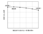
- FIG. 3 is a characteristic diagram showing simulation results of the relationship between the thickness of a QD layer that does not contain scattering particles and the light extraction efficiency in Example and Comparative Examples 1 and 2.
- FIG. 5 is a characteristic diagram showing simulation results of the relationship between the position in the wavelength conversion layer and the amount of excitation light absorbed per unit length in Example and Comparative Examples 1 and 2;
- FIG. 2 is a schematic cross-sectional view showing an example of a configuration of a light-emitting unit including a plurality of light-emitting devices shown in FIG.
- FIG. 1; 2 is a schematic cross-sectional view showing another example of the configuration of a light-emitting unit including a plurality of light-emitting devices shown in FIG. 1.
- FIG. It is a cross-sectional schematic diagram showing an example of a configuration of a light-emitting device according to Modification 1 of the present disclosure.
- FIG. 10 is a schematic cross-sectional view showing an example of a configuration of a light-emitting device according to Modification 2 of the present disclosure;
- FIG. 10 is a schematic cross-sectional view showing an example of a configuration of a light-emitting device according to Modification 3 of the present disclosure;
- FIG. 10 is a schematic cross-sectional view showing an example of a configuration of a light-emitting device according to Modification 4 of the present disclosure
- FIG. 11 is a schematic cross-sectional view showing an example of a configuration of a light-emitting device according to Modification 5 of the present disclosure
- FIG. 11 is a schematic cross-sectional view showing an example of a configuration of a light-emitting device according to Modification 6 of the present disclosure
- FIG. 12 is a schematic cross-sectional view showing an example of a configuration of a light-emitting device according to Modification 7 of the present disclosure
- FIG. 12 is a schematic cross-sectional view showing an example of a configuration of a light-emitting device according to Modification 8 of the present disclosure
- FIG. 21 is a schematic cross-sectional view showing an example of a configuration of a light-emitting unit according to Modification 9 of the present disclosure
- FIG. 20 is a schematic cross-sectional view showing an example of a configuration of a light-emitting unit according to Modification 10 of the present disclosure
- FIG. 21 is a schematic cross-sectional view showing an example of a configuration of a light-emitting unit according to Modification 11 of the present disclosure
- FIG. 12 is a cross-sectional schematic diagram showing an example of a cross-sectional configuration of a wavelength conversion layer according to Modification 12 of the present disclosure.
- FIG. 9 is a schematic cross-sectional view showing an example of a configuration of a light-emitting unit according to Modification 9 of the present disclosure
- FIG. 20 is a schematic cross-sectional view showing an example of a configuration of a light-emitting unit according to Modification 10 of the present disclosure
- FIG. 21 is a schematic cross-sectional view showing an example of a
- FIG. 21 is a schematic cross-sectional view showing an example of a configuration of a light-emitting device according to Modification 13 of the present disclosure
- 1 is a perspective view showing an example of a configuration of an image display device according to Application Example 1 of the present disclosure
- FIG. 21 is a schematic diagram showing an example of the layout of the image display device shown in FIG. 20
- FIG. It is a pixel circuit diagram of an active matrix drive system.
- FIG. 11 is a perspective view showing an example of a configuration of an image display device according to Application Example 2 of the present disclosure
- 24 is a perspective view showing the configuration of the mounting board shown in FIG. 23
- FIG. 25 is a perspective view showing the configuration of the unit board shown in FIG. 24;
- FIG. FIG. 11 is a diagram illustrating an example of an image display device according to Application Example 3 of the present disclosure;
- Embodiment (example of light-emitting device in which scattering particles are selectively dispersed on the light extraction surface side) 1-1. Configuration of Light Emitting Device 1-2. Configuration of Light Emitting Unit 1-3. Action and effect 2. Modified example 1 (an example in which the concentration of scattering particles is changed between the light source side and the light extraction surface side) 3.
- Modified example 2 (an example in which the concentration of the quantum dot phosphor is changed between the light source side and the light extraction surface side) 4.
- Modified example 3 (an example in which the configuration of the quantum dot phosphor is changed between the light source side and the light extraction surface side) 5.
- Modified example 4 (an example in which a resin layer is provided between the light source side and the light extraction surface side) 6.
- Modification 5 (an example in which a region containing only scattering particles is provided on the light source side) 7.
- Modification 6 (example using Cd-based quantum dot phosphor and Cd-free quantum dot phosphor) 8.
- Modified example 7 (an example in which the concentration of scattering particles in the in-plane direction is changed on the light extraction surface side) 9.
- Modification 8 (example in which the side surface of the wavelength conversion layer is inclined) 10.
- Modification 9 (Example of a light-emitting unit in which a microlens array is arranged on the light extraction surface) 11.
- Modification 10 (Another example of the configuration of the wavelength conversion layer of the blue light emitting device) 12.
- Modification 11 (Example of light-emitting unit in which color filters are arranged on the light extraction surface) 13.
- Modification 12 (another example of the structure of the wavelength conversion layer) 14.
- Modified Example 13 (example in which a textured structure is arranged on the light extraction surface) 15.
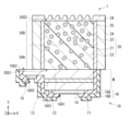
- FIG. 1 schematically illustrates an example of a cross-sectional configuration of a light-emitting device (light-emitting device 1) according to an embodiment of the present disclosure.
- the light-emitting device 1 is preferably used, for example, in the display pixels P of an image display device (eg, image display device 100, see FIG. 20).
- the light emitting device 1 of the present embodiment includes a light source unit 10 that emits excitation light EL, and a light emitting surface (surface 10S2) of the light source unit 10.
- the light emitting device 1 absorbs the excitation light EL and emits light of a different wavelength.
- a wavelength conversion layer 20 that The wavelength conversion layer 20 has, for example, a plurality of quantum dot phosphors 21 and a plurality of scattering particles 22 dispersed in a resin 23.
- the first region 20A and the second region are arranged in order from the surface 10S2 side of the light source unit 10. 20B.
- the first region 20A has a configuration in which only the plurality of quantum dot phosphors 21 are dispersed in the resin 23, and has a lower absorption coefficient of the excitation light EL than the second region 20B.
- the light source section 10 corresponds to a specific example of the "light source section" of the present disclosure.
- the light source unit 10 is a solid-state light-emitting device that emits light in a predetermined wavelength band from its upper surface (light-emitting surface), such as a light-emitting diode (LED) chip.
- LED light-emitting diode
- An LED chip refers to a chip cut out from a wafer used for crystal growth, not a package type covered with molded resin or the like.
- the LED chip has a size of, for example, 1 ⁇ m or more and 100 ⁇ m or less, and is called a micro LED.
- the light source section 10 has a first conductivity type layer 11, an active layer 12 and a second conductivity type layer 13 laminated in this order.
- the upper surface of the second conductivity type layer 13 is a light exit surface.
- the light source unit 10 has a columnar mesa portion M including a first conductivity type layer 11 and an active layer 12, and the first conductivity type layer 11 is exposed on the surface (surface 10S1) opposite to the light emitting surface. It has a step formed by a convex portion and a concave portion exposing the second conductivity type layer 13 .
- the surface opposite to the light extraction surface 10S2 (the surface 10S1 side) including the projections and recesses is the lower surface.
- the light source unit 10 further includes a first electrode 14 electrically connected to the first conductivity type layer 11 and a second electrode 15 electrically connected to the second conductivity type layer 13 .
- the first electrode 14 and the second electrode 15 are each provided on the surface 10S1 side.
- the first electrode 14 is arranged on the surface 10S1 of the first conductivity type layer, which is the convex portion on the lower surface
- the second electrode 15 is arranged on the surface 10S1 of the second conductivity type layer, which is the concave portion on the lower surface. are placed in
- the side surface of the light source section 10 made up of the first conductive layer 11, the active layer 12 and the second conductive layer 13 is covered with a laminated film 16 made up of an insulating film 16A and a reflective film 16B.
- the laminated film 16 extends, for example, to the periphery of the first electrode 14 and the second electrode 15, and has openings 16H1 and 16H2 on the first electrode 14 and the second electrode 15, respectively. That is, the first electrode and the second electrode are exposed to the outside through the openings 16H1 and 16H2, respectively.
- the materials forming the first conductivity type layer 11, the active layer 12 and the second conductivity type layer 13 are appropriately selected according to the desired wavelength band of light.
- the light source unit 10 may emit ultraviolet light having an emission wavelength of 360 nm or more and 430 nm or less, or blue band light having an emission wavelength of 430 nm or more and 500 nm or less (blue light ).
- Group III-V compound semiconductor materials include AlGaInN-based materials.
- a ZnSe-based material or a ZnO-based material may be used.
- the active layer 12 can be formed using, for example, a GaInN-based material.
- the light emitted from the light source unit 10 is not limited to ultraviolet light or blue light, and may be, for example, infrared light or red band light (red light).
- examples of III-V group compound semiconductor materials that emit infrared rays include AlGaInAs-based materials.
- III-V group compound semiconductor materials that emit red light include AlGaInP-based materials.
- the first electrode 14 is in contact with the first conductivity type layer 11 and is electrically connected to the first conductivity type layer 11 . That is, the first electrode 14 is in ohmic contact with the first conductivity type layer 11 .
- the first electrode 14 is, for example, a metal electrode, and is configured, for example, as a multilayer film (Ni/Au) of nickel (Ni) and gold (Au).
- the first electrode 14 may be made of a transparent conductive material such as indium tin oxide (ITO).
- the second electrode 15 is in contact with the second conductivity type layer 13 and is electrically connected to the second conductivity type layer 13 . That is, the second electrode 15 is in ohmic contact with the second conductivity type layer 13 .
- the second electrode 15 is, for example, a metal electrode, and is configured as, for example, a multilayer film (Ti/Al) of titanium (Ti) and aluminum (Al) or a multilayer film of chromium (Cr) and Au (Cr/Au). It is Alternatively, the second electrode 15 may be made of a transparent conductive material such as ITO.
- the laminated film 16 is formed from the side surface to the bottom surface of the light source section 10 as described above.
- the insulating film 16A and the reflective film 16B are thin films, respectively, and can be formed by thin film forming processes such as CVD, vapor deposition, and sputtering, for example.
- the insulating film 16A is for electrical insulation between the reflective film 16B and the first conductivity type layer 11, the active layer 12 and the second conductivity type layer 13. As shown in FIG.
- the insulating film 16A is preferably formed using a material transparent to light emitted from the active layer 12. As shown in FIG. Such materials include, for example, SiO 2 , Si 2 N 3 , Al 2 O 3 , TiO 2 and TiN.
- the thickness of the insulating film 16A is, for example, approximately 50 nm to 1 ⁇ m.
- the reflective film 16B is for reflecting the light emitted from the active layer 122.
- the reflective film 16B is provided with the insulating film 16A interposed therebetween.
- the reflective film 16B extends to the side surface and the lower surface of the light source unit 10, and is formed in the openings 16H1 and 16H2 of the insulating film 16A, for example, to a position slightly recessed from the end of the insulating film 16A.
- the reflective film 16B is insulated (electrically separated) from the first conductive layer 11, the active layer 12, the second conductive layer 13, the first electrode 14, and the second electrode 15 by the insulating film 16A.
- the reflective film 16B As a material for the reflective film 16B, it is preferable to use a material that reflects the light emitted from the active layer 12 to form it. Such materials include, for example, Ti, Al, silver (Ag), copper (Cu), Au, Ni, or alloys thereof.
- the thickness of the reflective film 16B is, for example, about 50 nm to 1 ⁇ m.
- An insulating film may be further formed on the reflective film 16B.
- the insulating film is preferably formed on the first electrode 14 and the second electrode 15 up to the insulating film 16A so as to cover the end portion of the reflective film 16B.
- the wavelength conversion layer 20 corresponds to a specific example of the "wavelength conversion layer" of the present disclosure.
- the wavelength conversion layer 20 is arranged on the surface 10S2 side of the light source unit 10, and converts the light emitted from the light source unit 10 into light of a desired wavelength band (eg, red light Lr, green light Lg, and blue light Lb). It is.
- the wavelength conversion layer 20 has a surface 20S1 and a surface 20S2 as a pair of surfaces facing each other.
- the surface 20S1 corresponds to the “first surface” of the present disclosure, and is arranged to face the surface 10S2 of the light source section 10 .
- the surface 20S2 corresponds to the “second surface” of the present disclosure, and serves as an extraction surface for wavelength-converted light.
- a plurality of quantum dot phosphors 21 and a plurality of scattering particles 22 are dispersed in the resin 23 as described above.
- the quantum dot phosphor 21 corresponds to a specific example of the "wavelength conversion material" of the present disclosure.
- the quantum dot phosphor 21 absorbs the light emitted from the light source section 10 as excitation light EL and emits fluorescence.
- the quantum dot phosphor 21 is, for example, a particulate phosphor that emits fluorescence in a blue wavelength band of 430 nm or more and 500 nm or less, a green wavelength band of 500 nm or more and 550 nm or less, or a red wavelength band of 610 nm or more and 780 nm or less. be.
- the quantum dot phosphor 21 can be selected from InP, GaInP, InAsP, CdSe, CdZnSe, CdTeSe, CdTe, or the like.
- the quantum dot phosphor 21 can be selected from, for example, InP, GaInP, ZnSeTe, ZnTe, CdSe, CdZnSe, CdS, CdSeS, and the like.
- the quantum dot phosphor 21 can be selected from ZnSe, ZnTe, ZnSeTe, CdSe, CdZnSe, CdS, CdZnS, CdSeS, and the like.
- the quantum dot phosphor 21 is not limited to the above, and for example, CuInSe 2 , CuInS 2 , CuInGaS, AgInS 2 or the like may be used.
- perovskite nanophosphors composed of CsPb(Cl/Br) 3 , CsPbBr 3 , CsPb(I/Br) 3 and CsPbI 3 may be used.
- the quantum dot phosphor 21 can also control the fluorescent color by its particle size. For example, the smaller the particle size, the shorter the fluorescence wavelength. In order to obtain fluorescence with high color purity, it is desirable to select a quantum dot phosphor whose particle size is controlled.
- the quantum dot phosphor 21 has an average particle size of, for example, 5 nm or more and 100 nm or less, and has a core/shell structure consisting of a core that emits light with an average particle size of about 2 nm to 10 nm, and a shell that covers and protects the core. .
- the shell consists of one layer or multiple layers.
- the shell may further be covered with an inorganic film such as silicon oxide ( SiO2 ) or aluminum oxide ( Al2O3 ).
- SiO2 silicon oxide
- Al2O3 aluminum oxide
- a large number of organic ligands are coordinated to the surface of the quantum dot phosphor 21, and the organic ligands cause aggregation of the quantum dot phosphor 21 when the quantum dot phosphor and the solvent are mixed. is suppressed and the dispersibility is improved.
- an inkjet or needle dispenser that ejects or applies the resin 23 mixed with the quantum dot phosphors 21 depending on the viscosity is used.
- This is classified as a plateless printing method, and in the above method, it is possible to selectively fill the quantum dot phosphor 21 only in the barrier, so the utilization efficiency of the quantum dot phosphor 21 can be improved.
- You may make it apply
- the quantum dot phosphor 21 may be applied to the entire base material by a spin coater, a PR method, or the like.
- an inorganic phosphor or an organic phosphor may be used as the wavelength conversion material.
- the scattering particles 22 scatter the excitation light EL emitted from the light source unit 10 and the fluorescence emitted from the quantum dot phosphor 21 to change the incident angle of the fluorescence to the light extraction surface 20S2, thereby improving the light extraction efficiency. It is for The scattering particles 22 are for increasing the effective optical path length of the excitation light EL, thereby improving the absorption rate of the excitation light EL. It is preferable that the scattering particles 22 have an average particle size larger than that of the quantum dot phosphor 21 and a refractive index larger than that of the resin 23 . For the scattering particles 22, it is preferable to use a dielectric substance having a particle size of, for example, 100 nm or more and 1000 nm or less.
- Specific materials of the scattering particles 22 include, for example, silicon oxide (SiO 2 ), titanium oxide (TiO 2 ), aluminum oxide (Al 2 O 3 ), aluminum nitride (AlN), boron nitride (BN) and zinc oxide. (ZnO) and the like.
- the scattering particles 22 may be, for example, air bubbles mixed in the filler 123 or aggregated quantum dot phosphors 21 .
- the resin 23 is for dispersing the quantum dot phosphors 21 and the scattering particles 22, and can be formed using, for example, a material having optical transparency to the excitation light EL.
- a specific material of the resin 23 for example, an ultraviolet curable resin or a thermosetting resin can be used.
- sol-gel glass or the like may be used.
- the resin 23 is not necessarily required, and the quantum dot phosphor 21 and the scattering particles 22 may be enclosed in the hollow structure.
- the wavelength conversion layer 20 has a first region 20A and a second region 20B that have different absorption coefficients for the excitation light EL in order from the surface 10S2 side of the light source section 10 .
- the first region 20 ⁇ /b>A does not include the plurality of scattering particles 22 in the resin 23 and has a configuration in which only the plurality of quantum dot phosphors 21 are dispersed.
- the second region 20 ⁇ /b>B has a configuration in which both the multiple quantum dot phosphors 21 and the multiple scattering particles 22 are dispersed in the resin 23 . Accordingly, the first region 20A has a lower absorption coefficient of the excitation light EL than the second region 20B.
- FIG. 2 shows simulation results of the relationship between the thickness of the QD layer (wavelength conversion layer 20) that does not contain the scattering particles 22 and the light extraction efficiency in Example and Comparative Examples 1 and 2.
- FIG. 3 shows simulation results of the relationship between the position in the wavelength conversion layer 20 and the amount of excitation light absorbed per unit length in Example and Comparative Examples 1 and 2.
- An example is a light-emitting device 1 having the above configuration.
- Comparative Example 1 is a light-emitting device in which a plurality of quantum dot phosphors 21 and a plurality of scattering particles are dispersed substantially uniformly throughout the resin 23 forming the wavelength conversion layer 20 .
- Comparative Example 2 is a light-emitting device in which only the plurality of quantum dot phosphors 21 are substantially uniformly dispersed throughout the resin 23 forming the wavelength conversion layer 20 without including the plurality of scattering particles 22 .
- the excitation light EL incident on the wavelength conversion layer 20 is scattered by the scattering particles 22 to increase the optical path length.
- the wavelength conversion layer 20 Example and Comparative Example 2 in which the plurality of scattering particles 22 are dispersed together with the plurality of quantum dot phosphors 21 does not contain the plurality of scattering particles 22 (Comparative Example 2).
- the absorption rate of the excitation light EL in the wavelength conversion layer 20 increases.
- the fluorescence emitted from the quantum dot phosphor 21 is scattered by the scattering particles 22, thereby improving the light extraction efficiency (FIG. 2).
- the temperature of the wavelength conversion layer 20 rises due to the heat generated by the quantum dot phosphors 21 due to the absorption of the excitation light EL. deterioration is more likely to occur.
- the heat generation of the quantum dot phosphor 21 due to the absorption of the excitation light EL becomes remarkable in the vicinity of the light source section 10 .
- the first region 20A in which only the plurality of quantum dot phosphors 21 are dispersed without including the plurality of scattering particles 22 in the resin 23 is provided on the light source unit 10 side.
- the light density in the vicinity of the light source section 10 side is reduced, and the absorption amount of the excitation light EL per unit length is reduced to approximately the same level as in Comparative Example 2 (FIG. 3). Therefore, temperature rise in the vicinity of the light source unit 10 is suppressed, and deterioration of the quantum dot phosphor 21 is reduced.
- a side surface (surface 20S3) of the wavelength conversion layer 20 is sealed by a side wall 24, for example.
- materials forming the sidewall 24 include SiO 2 , silicon (Si), resist, resin, and metal materials such as Cu and Al.
- a light reflecting film 25 may be formed between the wavelength conversion layer 20 and the sidewall 24 .
- the light reflecting film 25 is for reflecting the excitation light EL emitted from the light source unit 10 and scattered by the scattering particles 22 and fluorescence emitted from the quantum dot phosphor 21 into the wavelength conversion layer 20.
- the light reflecting film 25 is preferably formed using a material that has a high reflectance with respect to the excitation light EL and fluorescence regardless of the light incident angle. Examples of materials for the light reflecting film 25 include metal materials such as gold (Au), Ag , aluminum (Al ) and platinum (Pt ) ; A dielectric multilayer film in which 2 O 3 is combined is exemplified.
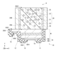
- FIG. 4 schematically shows a cross-sectional configuration of the light emitting unit 2. As shown in FIG.
- the light-emitting unit 2 is, for example, a plurality of light-emitting devices 1 arranged in a row.
- the light emitting unit 2 has, for example, an elongated shape extending in the arrangement direction of the plurality of light emitting devices 1 .
- the display pixels P of the image display device 100 include, for example, three color pixels Pr, Pg, and Pb corresponding to RGB, and the color pixels Pr, Pg, and Pb respectively emit light in corresponding wavelength bands.
- a light emitting device 1 is provided.
- FIG. 4 schematically shows an example of the cross-sectional configuration of the light emitting unit 2. As shown in FIG.
- the light-emitting unit 2 is composed of light-emitting devices 1R, 1G, and 1B that emit light corresponding to respective color pixels Pr, Pg, and Pb.
- the color pixel Pr has a light emitting device 1R that emits light in the red band (red light Lr)
- the color pixel Pg has a light emitting device 1G that emits light in the green band (green light Lg)
- the color pixel Pb has a light emitting device 1G that emits light in the green band (green light Lg).
- a light-emitting device 1B that emits light in the band (blue light Lb) is provided.
- the light-emitting unit 2 has an elongated shape extending in the arrangement direction of the light-emitting devices 1, the light-emitting device 1R is arranged, for example, near the short side of the light-emitting unit 2, and the light-emitting device 1B is arranged, for example, , near a short side of the light emitting unit 2 that is different from the adjacent short side of the light emitting device 1B.
- the light emitting device 1G is arranged, for example, between the light emitting device 1R and the light emitting device 1B.
- the positions of the light emitting devices 1R, 1G, and 1B are not limited to the above.
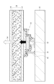
- the light emitting devices 1R, 1G and 1B are mounted on the driving substrate 41 via pad electrodes 42 and 43 and bumps 44 and 45, respectively. It should be noted that other bonding methods such as Cu—Cu bonding may be used for mounting on the drive substrate 41 .
- Each of the light emitting devices 1R, 1G, and 1B includes, for example, a plurality of quantum dot phosphors 21 for wavelength-converting the excitation light EL into light in a predetermined wavelength band on the light source unit 10 that emits blue light as the excitation light EL.
- a conversion layer 20 is arranged.
- a plurality of quantum dot phosphors 21 that emit red fluorescence and a plurality of scattering particles 22 are dispersed in the resin 23, and the excitation emitted from the light source unit 10
- the light EL is converted into red light by the quantum dot phosphor 21 and scattered by the scattering particles 22 to be taken out as red light Lr.
- a plurality of quantum dot phosphors 21 emitting green fluorescence and a plurality of scattering particles 22 are dispersed in a resin 23, and the excitation light EL emitted from the light source unit 10 is converted into green light by the quantum dot phosphor 21 and scattered by the scattering particles 22 to be taken out as green light Lg.
- the wavelength conversion layer 20 arranged in the light emitting device 1B for example, only the scattering particles 22 are dispersed in the resin 23, and the excitation light EL emitted from the light source section 10 is scattered by the scattering particles 22 and becomes blue light. Taken out as Lb.
- an excitation light reflection film 31 may be provided as a wavelength selection layer for selectively reflecting the excitation light EL on the wavelength conversion layer 20 of the light emitting devices 1R and 1G.
- the excitation light EL emitted from the light extraction surface 20S2 of the wavelength conversion layer 20 is reduced, and the color gamut can be improved.
- the contrast of external light can be improved.
- a yellow filter that selectively absorbs blue light may be arranged.
- the excitation light EL When the light source unit 10 that emits ultraviolet rays is used as the excitation light EL, for example, as shown in FIG. A wavelength conversion layer 20 in which a quantum dot phosphor 21 and a plurality of scattering particles 22 are dispersed in a resin 23 is arranged. As a result, the excitation light EL emitted from the light source section 10 in the light emitting device 1B is converted into blue light by the quantum dot phosphor 21 and scattered by the scattering particles 22 to be extracted as blue light Lb.
- the excitation light reflection film 31 is also arranged on the light emitting device 1B.
- the wavelength conversion layer 20 has the first region 20A and the second region 20B from the light source section 10 side, and the first region 20A contains only the plurality of quantum dot phosphors 21 in the resin 23. Both the plurality of quantum dot phosphors 21 and the plurality of scattering particles 22 are dispersed in the resin 23 in the second region 20B, and the first region 20A has a lower absorption of the excitation light EL than the second region 20B. coefficient. This reduces the absorption rate of the excitation light EL in the vicinity of the light source unit 10 . This will be explained below.
- a display device for augmented reality (AR) applications has been developed that combines a blue LED array with a color conversion layer using quantum dots (QDs).
- QDs quantum dots
- a QD layer with high color conversion efficiency is required in order to increase luminance and reduce power consumption.
- the color conversion efficiency of the QD layer in addition to the quantum yield of the QD, the light extraction efficiency from the QD layer is also important. For example, since the fluorescence emitted from the QDs emits isotropic light, the total reflection of the high-angle component at the interface between the QDs and the air reduces the amount of fluorescence extracted into the air.
- a method of adding scatterers to the QD layer is used.
- the addition of the scatterer also increases the optical path length of the excitation light in the QD layer, thereby providing the advantage of increasing the absorption rate of the excitation light. Accordingly, by adding a scatterer to the QD layer, the color conversion efficiency of the QD layer can be improved.
- the region of the QD layer near the LED has the highest light density and the highest temperature, resulting in greater degradation of the QDs. Since the excitation light absorptance in the vicinity of the LED becomes higher in the presence of the scatterer, the temperature of the QD layer in the vicinity of the LED becomes higher and the reliability deteriorates.
- the attained luminance of a light-emitting element using a color conversion layer of QDs is often rate-determined by reliability. For this reason, in order to improve the luminance of a light-emitting device, it becomes a challenge to achieve both light extraction efficiency and reliability of the device structure.
- an LED device has been proposed in which a layer (scatterer layer) to which only scatterers are added is added between the LED and the QD layer to which scatterers are added.
- the scatterer between the LED and the QD layer makes the excitation light uniform in the lateral direction, and the distance between the LED and the QD layer increases the area of the excitation light, thereby improving reliability.
- the scatterer layer causes the excitation light to return from the LED to the inside of the LED, thereby reducing the amount of light incident on the QD layer, thereby reducing the light extraction efficiency of the combined LED and color conversion layer.
- the angle of the QD sidewalls becomes vertical, which limits the effect of reducing the light density by increasing the distance between the LED and the QD.
- the first region 20A is provided by dispersing only the plurality of quantum dot phosphors 21 in the resin 23 on the light source section 10 side, and the resin 23 is provided on the light extraction surface 20S2 side.
- a second region 20B is provided in which both the plurality of quantum dot phosphors 21 and the plurality of scattering particles 22 are dispersed.
- the light-emitting device 1 of the present embodiment it is possible to achieve both an improvement in light extraction efficiency and an improvement in reliability.
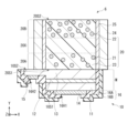
- FIG. 6 schematically illustrates an example of a cross-sectional configuration of a light-emitting device (light-emitting device 3) according to Modification 1 of the present disclosure.
- This light-emitting device 3 like the light-emitting device 1 in the above-described embodiment, is suitably used for, for example, the display pixels P of an image display device (for example, the image display device 100).
- only the plurality of quantum dot phosphors 21 are dispersed in the resin 23 in the first region 20A on the light source unit 10 side, and the absorption coefficient of the excitation light EL in the vicinity of the light source unit 10 is changed to the excitation light EL in the vicinity of the light extraction surface 20S2.
- An example in which the absorption coefficient is lower than the absorption coefficient of the optical EL is shown, but the present invention is not limited to this.
- a plurality of scattering particles 22 may be dispersed in the first region 20A at a concentration lower than the concentration of the plurality of scattering particles in the second region 20B.
- both the plurality of quantum dot phosphors 21 and the plurality of scattering particles 22 are dispersed in the first region 20A, and the concentration of the plurality of scattering particles in the first region 20A is It was made lower than the concentration of a plurality of scattering particles. This makes it possible to obtain the same effects as those of the above-described embodiment.
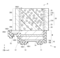
- FIG. 7 schematically illustrates an example of a cross-sectional configuration of a light-emitting device (light-emitting device 4) according to Modification 2 of the present disclosure.
- the light-emitting device 4 like the light-emitting device 1 in the above-described embodiment, is suitably used for, for example, the display pixels P of an image display device (for example, the image display device 100).
- the concentration of the plurality of quantum dot phosphors 21 dispersed in the first region 20A may be made lower than the concentration of the plurality of quantum dot phosphors 21 dispersed in the second region 20B.
- the concentration of the plurality of quantum dot phosphors 21 in the first region 20A is made lower than the concentration of the plurality of scattering particles in the second region 20B.
- the amount of heat generated in the first region 20A is further reduced compared to the above-described embodiment, and the reliability can be further improved. Further, compared to the above embodiment, higher luminance can be achieved.
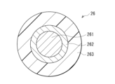
- FIG. 8 schematically illustrates an example of a cross-sectional configuration of a light-emitting device (light-emitting device 5) according to Modification 3 of the present disclosure.
- This light-emitting device 5 like the light-emitting device 1 in the above-described embodiment, is suitably used for, for example, the display pixels P of an image display device (for example, the image display device 100).
- a plurality of quantum dot phosphors 26 having a different material, composition, or core/shell structure from the plurality of quantum dot phosphors 21 dispersed in the second region 20B may be dispersed in the first region 20A.
- quantum dot phosphors 26 having a lower absorption coefficient of the excitation light EL than the quantum dot phosphors 21 dispersed in the second region 20B are dispersed.
- FIG. 9 schematically shows the cross-sectional configuration of the quantum dot phosphor 26.
- the absorption coefficient of the quantum dot phosphor 26 can be controlled by, for example, changing the thickness ratio of the core 261 and the shell A 262 and shell B 263 covering the core 261 .
- the quantum dot phosphors 26 having a lower absorption coefficient of the excitation light EL than the quantum dot phosphors 21 dispersed in the second region 20B are dispersed in the first region 20A.
- the amount of heat generated in the first region 20A is further reduced compared to the above-described embodiment, and the reliability can be further improved. Further, compared to the above embodiment, higher luminance can be achieved.
- FIG. 10 schematically illustrates an example of a cross-sectional configuration of a light-emitting device (light-emitting device 6) according to Modification 4 of the present disclosure.
- This light-emitting device 6 like the light-emitting device 1 in the above-described embodiment, is suitably used for, for example, the display pixels P of an image display device (for example, the image display device 100).
- the plurality of quantum dot phosphors 21 are dispersed in the resin 23 in the first region 20A on the light source unit 10 side, and the absorption coefficient of the excitation light EL in the vicinity of the light source unit 10 is changed to the excitation light EL in the vicinity of the light extraction surface 20S2.
- An example in which the absorption coefficient is lower than the absorption coefficient of the optical EL is shown, but the present invention is not limited to this.
- a region 20X made only of the resin 23 may be provided between the first region 20A in which only the plurality of quantum dot phosphors 21 are dispersed in the resin 23 and the second region 20B in which both the plurality of quantum dot phosphors 21 and the plurality of scattering particles 22 are dispersed .
- the region 20X made only of the resin 23 is provided between the first region 20A and the second region 20B so as to spatially separate the first region 20A and the second region 20B. made it As a result, it is possible to reduce the influence of heat generation on the first region 20A with respect to the second region 20B. Therefore, the reliability can be further improved as compared with the above embodiment. Further, compared to the above embodiment, higher luminance can be achieved.
- FIG. 11 schematically illustrates an example of a cross-sectional configuration of a light-emitting device (light-emitting device 7) according to Modification 5 of the present disclosure.
- This light-emitting device 7 is suitably used for, for example, the display pixels P of an image display device (for example, the image display device 100), like the light-emitting device 1 in the above embodiment.
- the first region 20A in which only the plurality of quantum dot phosphors 21 are dispersed in the resin 23 and the second region 20B in which both the plurality of quantum dot phosphors 21 and the plurality of scattering particles 22 are dispersed are provided in this order from the light source unit 10 side, but the configuration of the wavelength conversion layer 20 is not limited to this.
- the wavelength conversion layer 20 is divided into, for example, three regions, a first region 20A, a second region 20B, and a third region 20C, from the light source unit 10 side, and the first region 20A contains only the plurality of scattering particles 22.
- the second region 20B and the third region 20C may have the same configurations as the first region 20A and the second region 20B of the above embodiment, respectively.
- the first region 20A, the second region 20B, and the third region 20C are divided from the light source unit 10 side, for example, into three regions, and only the plurality of scattering particles 22 are placed in the first region 20A. I tried to disperse it.
- the excitation light EL incident on the wavelength conversion layer 20 from the light source unit 10 is homogenized in the first region 20A, so that only the plurality of quantum dot phosphors 21 are incident on the second region 20B dispersed in the resin 23. In-plane uniformity of the excitation light EL can be improved. Therefore, the reliability can be further improved as compared with the above embodiment.
- FIG. 12 schematically illustrates an example of a cross-sectional configuration of a light-emitting device (light-emitting device 8) according to Modification 6 of the present disclosure.
- the light-emitting device 8 like the light-emitting device 1 in the above-described embodiment, is suitably used for, for example, the display pixels P of an image display device (for example, the image display device 100).
- the first region 20A in which only the plurality of quantum dot phosphors 21 are dispersed in the resin 23 and the second region 20B in which both the plurality of quantum dot phosphors 21 and the plurality of scattering particles 22 are dispersed are provided in this order from the light source unit 10 side, but the configuration of the wavelength conversion layer 20 is not limited to this.
- a third region 20C in which both the plurality of quantum dot phosphors 21B and the plurality of scattering particles 22 are dispersed may be further provided on the second region 20B of the above embodiment.
- the multiple quantum dot phosphors 21A dispersed in the first region 20A and the second region 20B are made of different materials from the multiple quantum dot phosphors 21B dispersed in the third region 20C.
- so-called Cd-based quantum dot phosphors have higher light resistance than Cd-free quantum dot phosphors.
- the Cd-based quantum dot phosphor is used for the first region 20A and the second region 20B, and the Cd-free quantum dot phosphor is used for the third region 20C.
- the first region 20A in which only the plurality of quantum dot phosphors 21 are dispersed in the resin 23 in the wavelength conversion layer 20 on the light source unit 10 side other regions (for example, the farthest from the light source unit 10) It becomes possible to use a Cd-free quantum dot phosphor for the third region 20C). Therefore, the Cd concentration in the wavelength conversion layer 20 can be reduced, and the environmental load can be reduced.
- FIG. 13 schematically illustrates an example of a cross-sectional configuration of a light-emitting device (light-emitting device 9) according to Modification 7 of the present disclosure.
- This light-emitting device 9 like the light-emitting device 1 in the above-described embodiment, is suitably used for, for example, the display pixels P of an image display device (for example, the image display device 100).
- the first region 20A in which only the plurality of quantum dot phosphors 21 are dispersed in the resin 23 and the second region 20B in which both the plurality of quantum dot phosphors 21 and the plurality of scattering particles 22 are dispersed are provided in this order from the light source unit 10 side, but the configuration of the wavelength conversion layer 20 is not limited to this.
- the first region 20A may extend toward the light extraction surface 20S2, and the first region 20A may be provided around the second region 20B.
- the concentration of the plurality of quantum dot phosphors 21 in the wavelength conversion layer 20 is also changed in the lateral direction.
- the light extraction efficiency is relatively high even near the center of the light emitting device 9 . Therefore, by combining with a microlens array 32 to be described later, it is possible to improve the controllability of the light distribution characteristics of the light emitting device 9 .
- FIG. 14 schematically illustrates an example of a cross-sectional configuration of a light-emitting device (light-emitting device 1) according to Modification 8 of the present disclosure.
- the side surface (surface 20S3) of wavelength conversion layer 20 is vertical is shown, but the present invention is not limited to this.
- the surface 20S3 of the wavelength conversion layer 20 may be an inclined surface extending from the surface 20S1 toward the surface 20S2. This makes it possible to further improve the light extraction efficiency of fluorescence emitted in the wavelength conversion layer 20 .
- FIG. 15 schematically illustrates an example of a cross-sectional configuration of a light-emitting unit (light-emitting unit 2A) according to Modification 9 of the present disclosure.
- a microlens array 32 may be provided on the light extraction surface 20S2 of the light emitting devices 1R, 1G, and 1B.
- the microlens array 32 corresponds to a specific example of the "light distribution control structure" of the present disclosure.
- a photonic crystal, a moth-eye structure, a nanoantenna, and a metamaterial may be provided. This makes it possible to increase the luminance on the low-angle side, for example.
- FIG. 16 schematically illustrates an example of a cross-sectional configuration of a light-emitting unit (light-emitting unit 2B) according to Modification 10 of the present disclosure.
- a plurality of scattering particles 22 are dispersed substantially uniformly in the wavelength conversion layer 20 arranged in the light emitting device 1B
- the present invention is not limited to this.
- the first region 20A and the second region 20B are provided, and the concentration of the plurality of scattering particles 22 in the second region 20B is higher than the concentration of the plurality of scattering particles 22 in the first region 20A. You can make it higher. This reduces the ratio of the excitation light EL returning to the light source unit 10 . Therefore, it is possible to improve the light extraction efficiency of the light emitting device 1B and reduce the power consumption.
- FIG. 17 schematically illustrates an example of a cross-sectional configuration of a light-emitting unit (light-emitting unit 2C) according to Modification 11 of the present disclosure.
- the corresponding red light Lr, green light Lg, and blue light Lb are emitted from the light emitting devices 1R, 1G, and 1B, but the present invention is not limited to this.
- white light is emitted from each wavelength conversion layer 20 of the light emitting devices 1R, 1G, and 1B, and corresponding color filters (red filters 33R , a green filter 33G and a blue filter 33B) may be provided. This eliminates the step of separately painting the wavelength conversion layer 20 for each of the color pixels Pr, Pg, and Pb, thus making it possible to reduce the manufacturing cost.
- FIG. 18 schematically illustrates another example of the cross-sectional configuration of the wavelength conversion layer 20 in Modification 12 of the present disclosure.
- the wavelength conversion layer 20 is made to emit white light Lw, and the top and bottom of the wavelength conversion layer 20 are sealed with, for example, barrier films 27 and 28 having light transmittance. It is good also as the wavelength conversion layer 20 of shape.
- Such a QD sheet can be used, for example, as a backlight for a liquid crystal display device.
- FIG. 19 schematically illustrates an example of a cross-sectional configuration of a light-emitting device (light-emitting device 1) according to Modification 13 of the present disclosure.
- a texture structure 34 may be further provided on the light extraction surface (surface 20S2) of the wavelength conversion layer 20.
- FIG. 19 As a result, of the fluorescence emitted from the wavelength conversion layer 20, the fluorescence whose angle is smaller than the critical angle while the fluorescence with the critical angle or more is repeatedly reflected in the wavelength conversion layer 20 can be extracted from the light extraction surface. Become. Therefore, in addition to the effects of the above embodiments, it is possible to achieve high luminance.
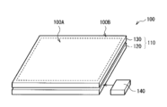
- FIG. 20 is a perspective view showing an example of a schematic configuration of an image display device (image display device 100).
- the image display device 100 is a so-called LED display, and the display pixels P use the light-emitting device (for example, the light-emitting device 1) of the present disclosure.
- the image display device 100 includes a display panel 110 and a control circuit 140 that controls driving of the display panel 110, as shown in FIG. 20, for example.
- the display panel 110 is obtained by superimposing a mounting substrate 120 and a counter substrate 130 on each other.
- the surface of the counter substrate 130 serves as an image display surface, and has a display area 100A in the central portion and a frame area 100B as a non-display area around it.
- FIG. 21 shows an example of the wiring layout of the area corresponding to the display area 100A on the surface of the mounting substrate 120 on the counter substrate 130 side.
- a region corresponding to the display region 100A on the surface of the mounting substrate 120 as shown in FIG. are placed.
- a plurality of scan wirings 1022 are formed extending in a direction intersecting (for example, perpendicular to) the data wirings 1021, and are arranged in parallel with a pitch of
- the data wiring 1021 and the scan wiring 1022 are made of a conductive material such as Cu, for example.
- the scan wiring 1022 is formed, for example, on the outermost layer, for example, on an insulating layer (not shown) formed on the base material surface.
- the base material of the mounting board 120 is made of, for example, a silicon substrate or a resin substrate, and the insulating layer on the base material is made of, for example, SiN, SiO, aluminum oxide (AlO), or a resin material.
- the data wiring 1021 is formed in a layer (for example, a layer below the outermost layer) different from the outermost layer including the scan wiring 1022, for example, formed in an insulating layer on the substrate. .
- black is provided as necessary.
- Black is for enhancing contrast and is composed of a light-absorbing material.
- the black is formed, for example, at least on areas where pad electrodes 1021B and 1022B, which will be described later, are not formed on the surface of the insulating layer. It should be noted that black can be omitted if necessary.
- Display pixels P are formed in the vicinity of the intersections of the data lines 1021 and the scan lines 1022, and a plurality of display pixels P are arranged, for example, in a matrix in the display area 100A.
- Each display pixel P is mounted with a light-emitting unit 2 including a plurality of light-emitting devices 1 corresponding to, for example, RGB.
- one display pixel P is composed of three light emitting devices 1R, 1G, and 1B, and red light is output from the light emitting device 1R, green light is output from the light emitting device 1G, and blue light is output from the light emitting device 1B. A case where it is possible to do so is exemplified.
- the image display device 100 shown in FIG. 20 is an example of a passive matrix image display device.
- the light emitting device 1 of the present embodiment can be applied not only to a passive matrix image display device (image display device 100), but also to an active matrix image display device. Note that the active matrix image display device does not require the frame region 100B shown in FIG. 20, for example.
- the passive matrix drive system In the passive matrix drive system, increasing the number of scan wires shortens the time allocated to each light emitting device, so the injection current must be increased as the duty ratio decreases, resulting in a decrease in luminous efficiency and device life. There is fear. To avoid this, it is necessary to lower the maximum brightness setting value.
- the screen is divided into multiple partial screens and passive matrix drive is used in parallel. , or a method of actively driving the light emitting device is adopted.
- Parallel passive matrix driving requires wiring to be pulled out to the back of each partial screen to connect the drive circuit, and the image signal must also be divided and parallelized according to each partial screen.
- a signal voltage holding and voltage-current conversion circuit is provided for each pixel, so that the above-described screen division is not performed, or at least in a state where the number of divisions is small, and higher luminance than passive matrix driving is obtained. be able to.
- FIG. 22 shows an example of a general active matrix driven pixel circuit.
- a switching transistor (Tr1), a driving transistor (Tr2), and a capacitive element (Cs) are provided for each display pixel P (light emitting devices 1R, 1G, 1B, near intersections between data wiring 1021 and scanning wiring 1022). are provided respectively.
- a switching transistor is used as a switch to write Vsig to a capacitive element, and in addition, the driving transistor is used as a current source for current control by the potential difference of power supply (Vcc)-Vsig to current-modulate the light-emitting device.
- the light emitting unit 2 is provided with a pair of terminal electrodes for each of the light emitting devices 1R, 1G, and 1B, for example.
- One terminal electrode is electrically connected to, for example, the data wiring 1021 and is electrically connected to the other terminal electrode, for example, the scan wiring 1022 .
- the terminal electrode is electrically connected to the pad electrode 1021B at the tip of the branch 1021A provided on the data line 1021.
- the terminal electrode is electrically connected to the pad electrode 1022B at the tip of the branch 1022A provided in the scan wiring 1022.
- the pad electrodes 1021B and 1022B are formed, for example, on the outermost layer, and are provided at the site where the light emitting unit 2 is mounted, for example, as shown in FIG.
- the pad electrodes 121B and 122B are made of a conductive material such as Au (gold).
- the mounting substrate 120 is further provided with, for example, a plurality of pillars (not shown) that regulate the distance between the mounting substrate 120 and the opposing substrate 130 .
- the struts may be provided in a region facing the display region 100A, or may be provided in a region facing the frame region 100B.
- the counter substrate 130 is made of, for example, a glass substrate or a resin substrate.
- the surface on the side of the light emitting device 1 may be flat, but is preferably rough.
- the rough surface may be provided over the entire region facing the display region 100A, or may be provided only in the region facing the display pixels P.
- the rough surface has fine unevenness on which light emitted from the display pixels P enters.
- the unevenness of the rough surface can be produced by sandblasting, dry etching, or the like, for example.
- the control circuit 140 drives each display pixel P (each light emitting unit 2) based on the video signal.
- the control circuit 140 includes, for example, a data driver that drives the data lines 1021 connected to the display pixels P and a scan driver that drives the scan lines 1022 connected to the display pixels P.
- FIG. 20 the control circuit 140 may be provided separately from the display panel 110 and connected to the mounting substrate 120 via wiring, or may be mounted on the mounting substrate 120.
- FIG. 23 is a perspective view showing another configuration example (image display device 200) of an image display device using the light emitting device (for example, light emitting device 1) of the present disclosure.
- the image display device 200 is a so-called tiling display.
- the image display device 200 includes, for example, a display panel 210 and a control circuit 240 that controls driving of the display panel 210, as shown in FIG.
- the display panel 210 is obtained by superimposing a mounting substrate 220 and a counter substrate 230 on each other.
- the surface of the counter substrate 230 serves as an image display surface, and has a display area in the central portion and a frame area as a non-display area around it (both not shown).
- the counter substrate 230 is arranged, for example, at a position facing the mounting substrate 220 with a predetermined gap therebetween. Note that the counter substrate 230 may be in contact with the top surface of the mounting substrate 220 .
- FIG. 24 schematically shows an example of the configuration of the mounting substrate 220.
- the mounting board 220 is composed of a plurality of unit boards 250 laid out like tiles. Note that FIG. 24 shows an example in which the mounting substrate 220 is configured by nine unit substrates 250, but the number of unit substrates 250 may be ten or more, or may be eight or less.
- the unit substrate 250 has, for example, a plurality of light emitting devices 1 laid out like tiles and a supporting substrate 260 supporting each light emitting device 1 .
- Each unit board 250 further has a control board (not shown).
- the support substrate 260 is composed of, for example, a metal frame (metal plate) or a wiring board. When the support substrate 260 is configured by a wiring substrate, it can also serve as a control substrate. At this time, at least one of the support substrate 260 and the control substrate is electrically connected to each light emitting device 1 .
- FIG. 26 shows the appearance of the transparent display 300.
- the transparent display 300 has, for example, a display section 310 , an operation section 311 and a housing 312 .
- the display unit 310 uses the light-emitting device of the present disclosure (for example, the light-emitting device 1).
- the transparent display 300 can display images and character information while the background of the display section 310 is transparent.
- a light-transmitting substrate is used as a mounting substrate.
- Each electrode provided in the light-emitting device 1 is formed using a conductive material having optical transparency, like the mounting substrate.
- each electrode has a structure that is difficult to see by narrowing the width of the wiring or thinning the thickness of the wiring.
- the transparent display 300 can perform black display by superimposing a liquid crystal layer having a driving circuit, for example, and can switch between transmission and black display by controlling the light distribution direction of the liquid crystal.
- the present invention is not limited to this.
- the light source unit 10 for example, an LED (OLED) using an organic semiconductor or a semiconductor laser (Laser Diode: LD) can be used.
- the light-emitting device for example, the light-emitting device 1 shown in the above embodiments and the like can be used in smartphones, televisions, notebook PCs, AR/VR equipment, projectors, head-up displays, in addition to the application examples 1 to 3 described above. (HUD), smart watches and video walls, etc.
- HUD head-up displays
- the present disclosure can also be configured as follows.
- a plurality of wavelength conversion materials and a plurality of scattering particles for converting first light emitted from the light source unit into second light having different wavelength bands are added to the wavelength conversion layer in the light source unit.
- the absorption coefficient of the first light in the vicinity of the side surface (first surface) is made lower than the absorption coefficient of the first light in the vicinity of the light extraction surface (second surface). This reduces the absorptance of the excitation light in the vicinity of the light source. Therefore, it is possible to achieve both light extraction efficiency and reliability.
- a light source unit having a light exit surface and emitting first light from the light exit surface;
- the light source unit has a first surface arranged on the light emitting surface side of the light source unit and arranged to face the light emitting surface and a second surface opposite to the first surface, and the first surface
- a light emitting device comprising: a wavelength converting layer having a lower absorption coefficient for said first light in its vicinity.
- the wavelength conversion layer has a first region and a second region in order from the first surface side, The light-emitting device according to (1), wherein the concentration of the plurality of scattering particles in the first region is lower than the concentration of the plurality of scattering particles in the second region. (3) The light-emitting device according to (2), wherein the first region does not include the plurality of scattering particles. (4) The wavelength conversion layer has a first region and a second region in order from the first surface side, any one of (1) to (3), wherein the concentration of the plurality of wavelength conversion materials in the first region is lower than the concentration of the plurality of wavelength conversion materials in the second region; A light emitting device as described.
- the wavelength conversion layer has a first region, a second region and a third region in order from the first surface side, the first region does not contain the plurality of wavelength converting materials and contains only the plurality of scattering particles; the second region does not contain the plurality of scattering particles and contains only the plurality of wavelength converting materials;
- the light emitting device according to any one of (1) to (6), wherein the third region comprises the plurality of wavelength converting materials and the plurality of scattering particles.
- the wavelength conversion layer has a first region, a second region and a third region in order from the first surface side, the first region does not include the plurality of scattering particles and only includes a plurality of first wavelength converting materials; said second region comprises said plurality of first wavelength converting materials and said plurality of scattering particles; said third region comprises a plurality of second wavelength converting materials and said plurality of scattering particles;
- the light emitting device according to any one of (1) to (6), wherein the first wavelength converting material has higher light resistance than the second wavelength converting material.
- the light-emitting device wherein the first wavelength conversion material is a cadmium-based quantum dot phosphor, and the second wavelength conversion material is a cadmium-free quantum dot phosphor.
- the wavelength conversion layer has a first region and a second region in order from the first surface side, The plurality of quantum dots contained in the first region and the second region are different from each other in material, composition, and core/shell structure. Any one of (1) to (9) above. luminous device.
- the first wavelength conversion layer converts the first light into red light
- the second wavelength conversion layer converts the first light into green light
- the light-emitting device according to any one of (1) to (13), wherein the third wavelength conversion layer transmits or converts the first light into blue light.
- the light emission according to (14) above further comprising a wavelength selective layer that selectively reflects the first light on at least the second surfaces of the first wavelength conversion layer and the second wavelength conversion layer.
- the light distribution control structure is any one of a microlens array, a photonic crystal, a moth-eye structure, a nanoantenna, and a metamaterial.
- the wavelength conversion layer a first wavelength conversion layer arranged on the light exit surface side of the first light source section, and a second wavelength conversion layer arranged on the light exit surface side of the second light source section.
- the first wavelength conversion layer, the second wavelength conversion layer and the third wavelength conversion layer each convert the first light into white light, a red filter that selectively transmits red light on the second surface of the first wavelength conversion layer; a green filter that selectively transmits green light on the second surface of the second wavelength conversion layer;
- the light emitting device is a light source unit having a light exit surface and emitting first light from the light exit surface;
- the light source unit has a first surface arranged on the light emitting surface side of the light source unit and arranged to face the light emitting surface and a second surface opposite to the first surface, and the first surface
- a wavelength conversion layer having a lower absorption coefficient than the first light in the vicinity thereof.
Abstract
A light-emitting device according to one embodiment of the present disclosure comprises: a light source unit that has a light emission surface and emits first light from the light emission surface; and a wavelength conversion layer that is positioned on the light emission surface-side of the light source unit, has a first surface positioned facing the light emission surface and a second surface on the reverse side from the first surface, and includes a plurality of wavelength conversion materials and a plurality of scattering particles for converting the first light into second light in a different wavelength band, the absorption coefficient of the first light in the vicinity of the first surface being lower than the absorption coefficient of the first light in the vicinity of the second surface.
Description
本開示は、発光デバイスおよびこれを備えた画像表示装置に関する。
The present disclosure relates to a light-emitting device and an image display device including the same.
例えば、特許文献1では、発光ダイオード(LED)素子上に光散乱材のみが分散された第1の樹脂層と、光散乱材および量子ドットが分散された第2の樹脂層とがこの順に積層された波長変換部材を備えたLED装置が開示されている。
For example, in Patent Document 1, a first resin layer in which only a light scattering material is dispersed on a light emitting diode (LED) element and a second resin layer in which a light scattering material and quantum dots are dispersed are laminated in this order. An LED device is disclosed that includes a wavelength converting member that is coated with a layer.
ところで、波長変換材料として量子ドットを用いた発光デバイスでは、光取り出し効率と信頼性との両立が求められている。
By the way, light-emitting devices using quantum dots as wavelength conversion materials are required to have both light extraction efficiency and reliability.
光取り出し効率と信頼性とを両立させることが可能な発光デバイスおよび画像表示装置を提供することが望ましい。
It is desirable to provide a light-emitting device and an image display device capable of achieving both light extraction efficiency and reliability.
本開示の一実施形態の発光デバイスは、光出射面を有し、第1の光を光出射面から出射する光源部と、光源部の光出射面側に配置され、光出射面と対向配置される第1の面および第1の面とは反対側の第2の面とを有すると共に、第1の光を波長帯域の異なる第2の光に変換する複数の波長変換材料および複数の散乱粒子を含み、第1の面の近傍における第1の光の吸収係数が、第2の面の近傍における第1の光の吸収係数よりも低い波長変換層とを備えたものである。
A light-emitting device according to an embodiment of the present disclosure includes a light-emitting surface, a light source section that emits first light from the light-emitting surface, and a light-emitting surface side of the light source section that faces the light-emitting surface. a plurality of wavelength-converting materials and a plurality of scatterers for converting first light into second light having a different wavelength band and having a first surface and a second surface opposite the first surface; and a wavelength conversion layer containing particles, wherein the absorption coefficient of the first light in the vicinity of the first surface is lower than the absorption coefficient of the first light in the vicinity of the second surface.
本開示の一実施形態の画像表示装置は、上記一実施形態の発光デバイスを備えたものである。
An image display device according to an embodiment of the present disclosure includes the light emitting device according to the above embodiment.
本開示の一実施形態の発光デバイスおよび一実施形態の画像表示装置では、光源部から出射される第1の光を波長帯域の異なる第2の光に変換する複数の波長変換材料および複数の散乱粒子を波長変換層において、光源部側の面(第1の面)近傍における第1の光の吸収係数が、光取り出し面(第2の面)近傍における第1の光の吸収係数よりも低くなるようにした。これにより、光源部近傍における励起光の吸収率を低減する。
In the light emitting device of one embodiment of the present disclosure and the image display device of one embodiment, a plurality of wavelength conversion materials for converting first light emitted from the light source unit into second light having a different wavelength band, and a plurality of scattering In the wavelength conversion layer, the absorption coefficient of the first light in the vicinity of the light source side surface (first surface) is lower than the absorption coefficient of the first light in the vicinity of the light extraction surface (second surface). I made it so that This reduces the absorptance of the excitation light in the vicinity of the light source.
以下、本開示における実施の形態について、図面を参照して詳細に説明する。以下の説明は本開示の一具体例であって、本開示は以下の態様に限定されるものではない。また、本開示は、各図に示す各構成要素の配置や寸法、寸法比等についても、それらに限定されるものではない。なお、説明する順序は、下記の通りである。
1.実施の形態(光取り出し面側に選択的に散乱粒子を分散させた発光デバイスの例)
1-1.発光デバイスの構成
1-2.発光ユニットの構成
1-3.作用・効果
2.変形例1(光源側と光取り出し面側とで散乱粒子の濃度を変えた例)
3.変形例2(光源側と光取り出し面側とで量子ドット蛍光体の濃度を変えた例)
4.変形例3(光源側と光取り出し面側とで量子ドット蛍光体の構成を変えた例)
5.変形例4(光源側と光取り出し面側との間に樹脂層を設けた例)
6.変形例5(光源部側に散乱粒子のみを含む領域を設けた例)
7.変形例6(Cd系量子ドット蛍光体とCdフリー量子ドット蛍光体とを用いた例)
8.変形例7(光取り出し面側において面内方向の散乱粒子の濃度を変えた例)
9.変形例8(波長変換層の側面を傾斜面とした例)
10.変形例9(光取り出し面にマイクロレンズアレイを配置した発光ユニットの例)
11.変形例10(青色発光デバイスの波長変換層の構成の他の例)
12.変形例11(光取り出し面にカラーフィルタを配置した発光ユニットの例)
13.変形例12(波長変換層の構造の他の例)
14.変形例13(光取り出し面にテクスチャ構造を配置した例)
15.適用例 Hereinafter, embodiments of the present disclosure will be described in detail with reference to the drawings. The following description is a specific example of the present disclosure, and the present disclosure is not limited to the following aspects. In addition, the present disclosure is not limited to the arrangement, dimensions, dimensional ratios, etc. of each component shown in each drawing. The order of explanation is as follows.
1. Embodiment (example of light-emitting device in which scattering particles are selectively dispersed on the light extraction surface side)
1-1. Configuration of Light Emitting Device 1-2. Configuration of Light Emitting Unit 1-3. Action andeffect 2. Modified example 1 (an example in which the concentration of scattering particles is changed between the light source side and the light extraction surface side)
3. Modified example 2 (an example in which the concentration of the quantum dot phosphor is changed between the light source side and the light extraction surface side)
4. Modified example 3 (an example in which the configuration of the quantum dot phosphor is changed between the light source side and the light extraction surface side)
5. Modified example 4 (an example in which a resin layer is provided between the light source side and the light extraction surface side)
6. Modification 5 (an example in which a region containing only scattering particles is provided on the light source side)
7. Modification 6 (example using Cd-based quantum dot phosphor and Cd-free quantum dot phosphor)
8. Modified example 7 (an example in which the concentration of scattering particles in the in-plane direction is changed on the light extraction surface side)
9. Modification 8 (example in which the side surface of the wavelength conversion layer is inclined)
10. Modification 9 (Example of a light-emitting unit in which a microlens array is arranged on the light extraction surface)
11. Modification 10 (Another example of the configuration of the wavelength conversion layer of the blue light emitting device)
12. Modification 11 (Example of light-emitting unit in which color filters are arranged on the light extraction surface)
13. Modification 12 (another example of the structure of the wavelength conversion layer)
14. Modified Example 13 (example in which a textured structure is arranged on the light extraction surface)
15. Application example
1.実施の形態(光取り出し面側に選択的に散乱粒子を分散させた発光デバイスの例)
1-1.発光デバイスの構成
1-2.発光ユニットの構成
1-3.作用・効果
2.変形例1(光源側と光取り出し面側とで散乱粒子の濃度を変えた例)
3.変形例2(光源側と光取り出し面側とで量子ドット蛍光体の濃度を変えた例)
4.変形例3(光源側と光取り出し面側とで量子ドット蛍光体の構成を変えた例)
5.変形例4(光源側と光取り出し面側との間に樹脂層を設けた例)
6.変形例5(光源部側に散乱粒子のみを含む領域を設けた例)
7.変形例6(Cd系量子ドット蛍光体とCdフリー量子ドット蛍光体とを用いた例)
8.変形例7(光取り出し面側において面内方向の散乱粒子の濃度を変えた例)
9.変形例8(波長変換層の側面を傾斜面とした例)
10.変形例9(光取り出し面にマイクロレンズアレイを配置した発光ユニットの例)
11.変形例10(青色発光デバイスの波長変換層の構成の他の例)
12.変形例11(光取り出し面にカラーフィルタを配置した発光ユニットの例)
13.変形例12(波長変換層の構造の他の例)
14.変形例13(光取り出し面にテクスチャ構造を配置した例)
15.適用例 Hereinafter, embodiments of the present disclosure will be described in detail with reference to the drawings. The following description is a specific example of the present disclosure, and the present disclosure is not limited to the following aspects. In addition, the present disclosure is not limited to the arrangement, dimensions, dimensional ratios, etc. of each component shown in each drawing. The order of explanation is as follows.
1. Embodiment (example of light-emitting device in which scattering particles are selectively dispersed on the light extraction surface side)
1-1. Configuration of Light Emitting Device 1-2. Configuration of Light Emitting Unit 1-3. Action and
3. Modified example 2 (an example in which the concentration of the quantum dot phosphor is changed between the light source side and the light extraction surface side)
4. Modified example 3 (an example in which the configuration of the quantum dot phosphor is changed between the light source side and the light extraction surface side)
5. Modified example 4 (an example in which a resin layer is provided between the light source side and the light extraction surface side)
6. Modification 5 (an example in which a region containing only scattering particles is provided on the light source side)
7. Modification 6 (example using Cd-based quantum dot phosphor and Cd-free quantum dot phosphor)
8. Modified example 7 (an example in which the concentration of scattering particles in the in-plane direction is changed on the light extraction surface side)
9. Modification 8 (example in which the side surface of the wavelength conversion layer is inclined)
10. Modification 9 (Example of a light-emitting unit in which a microlens array is arranged on the light extraction surface)
11. Modification 10 (Another example of the configuration of the wavelength conversion layer of the blue light emitting device)
12. Modification 11 (Example of light-emitting unit in which color filters are arranged on the light extraction surface)
13. Modification 12 (another example of the structure of the wavelength conversion layer)
14. Modified Example 13 (example in which a textured structure is arranged on the light extraction surface)
15. Application example
<1.実施の形態>
図1は、本開示の一実施の形態に係る発光デバイス(発光デバイス1)の断面構成の一例を模式的に表したものである。発光デバイス1は、例えば、画像表示装置(例えば、画像表示装置100、図20参照)の表示画素Pに好適に用いられるものである。 <1. Embodiment>
FIG. 1 schematically illustrates an example of a cross-sectional configuration of a light-emitting device (light-emitting device 1) according to an embodiment of the present disclosure. The light-emitting device 1 is preferably used, for example, in the display pixels P of an image display device (eg, image display device 100, see FIG. 20).
図1は、本開示の一実施の形態に係る発光デバイス(発光デバイス1)の断面構成の一例を模式的に表したものである。発光デバイス1は、例えば、画像表示装置(例えば、画像表示装置100、図20参照)の表示画素Pに好適に用いられるものである。 <1. Embodiment>
FIG. 1 schematically illustrates an example of a cross-sectional configuration of a light-emitting device (light-emitting device 1) according to an embodiment of the present disclosure. The light-
本実施の形態の発光デバイス1は、励起光ELを出射する光源部10と、光源部10の光出射面(面10S2)側に配置され、励起光ELを吸収して異なる波長の光を出射する波長変換層20とを有する。波長変換層20は、例えば、複数の量子ドット蛍光体21および複数の散乱粒子22が樹脂23中に分散されたものであり、光源部10の面10S2側から順に第1領域20Aおよび第2領域20Bを有する。第1領域20Aは、樹脂23中に複数の量子ドット蛍光体21のみ分散された構成となっており、第2領域20Bよりも低い励起光ELの吸収係数を有している。
The light emitting device 1 of the present embodiment includes a light source unit 10 that emits excitation light EL, and a light emitting surface (surface 10S2) of the light source unit 10. The light emitting device 1 absorbs the excitation light EL and emits light of a different wavelength. and a wavelength conversion layer 20 that The wavelength conversion layer 20 has, for example, a plurality of quantum dot phosphors 21 and a plurality of scattering particles 22 dispersed in a resin 23. The first region 20A and the second region are arranged in order from the surface 10S2 side of the light source unit 10. 20B. The first region 20A has a configuration in which only the plurality of quantum dot phosphors 21 are dispersed in the resin 23, and has a lower absorption coefficient of the excitation light EL than the second region 20B.
(1-1.発光デバイスの構成)
光源部10は、本開示の「光源部」の一具体例に相当するものである。光源部10は、所定の波長帯の光を上面(光出射面)から出射する固体発光素子であり、例えば発光ダイオード(LED)チップである。LEDチップとは、結晶成長に用いたウェハから切り出した状態のものを指しており、成形した樹脂等で覆われたパッケージタイプのものではないことを指している。LEDチップは、例えば1μm以上100μm以下のサイズとなっており、いわゆるマイクロLEDと呼ばれるものである。 (1-1. Configuration of Light Emitting Device)
Thelight source section 10 corresponds to a specific example of the "light source section" of the present disclosure. The light source unit 10 is a solid-state light-emitting device that emits light in a predetermined wavelength band from its upper surface (light-emitting surface), such as a light-emitting diode (LED) chip. An LED chip refers to a chip cut out from a wafer used for crystal growth, not a package type covered with molded resin or the like. The LED chip has a size of, for example, 1 μm or more and 100 μm or less, and is called a micro LED.
光源部10は、本開示の「光源部」の一具体例に相当するものである。光源部10は、所定の波長帯の光を上面(光出射面)から出射する固体発光素子であり、例えば発光ダイオード(LED)チップである。LEDチップとは、結晶成長に用いたウェハから切り出した状態のものを指しており、成形した樹脂等で覆われたパッケージタイプのものではないことを指している。LEDチップは、例えば1μm以上100μm以下のサイズとなっており、いわゆるマイクロLEDと呼ばれるものである。 (1-1. Configuration of Light Emitting Device)
The
光源部10は、第1導電型層11、活性層12および第2導電型層13がこの順に積層されている。第2導電型層13の上面は光出射面となっている。光源部10は、第1導電型層11および活性層12を含む柱状のメサ部Mを有し、光出射面とは反対側の面(面10S1)には、第1導電型層11が露出する凸部と、第2導電型層13が露出する凹部とからなる段差を有する。本実施の形態では、この凸部および凹部を含む、光取り出し面10S2とは反対側の面(面10S1側)を下面とする。光源部10は、さらに、第1導電型層11と電気的に接続される第1電極14および第2導電型層13と電気的に接続される第2電極15をする。第1電極14および第2電極15は、それぞれ、面10S1側に設けられている。具体的には、第1電極14は、下面の凸部である第1導電型層の面10S1上に配置され、第2電極15は、下面の凹部である第2導電型層の面10S1上に配置されている。
The light source section 10 has a first conductivity type layer 11, an active layer 12 and a second conductivity type layer 13 laminated in this order. The upper surface of the second conductivity type layer 13 is a light exit surface. The light source unit 10 has a columnar mesa portion M including a first conductivity type layer 11 and an active layer 12, and the first conductivity type layer 11 is exposed on the surface (surface 10S1) opposite to the light emitting surface. It has a step formed by a convex portion and a concave portion exposing the second conductivity type layer 13 . In the present embodiment, the surface opposite to the light extraction surface 10S2 (the surface 10S1 side) including the projections and recesses is the lower surface. The light source unit 10 further includes a first electrode 14 electrically connected to the first conductivity type layer 11 and a second electrode 15 electrically connected to the second conductivity type layer 13 . The first electrode 14 and the second electrode 15 are each provided on the surface 10S1 side. Specifically, the first electrode 14 is arranged on the surface 10S1 of the first conductivity type layer, which is the convex portion on the lower surface, and the second electrode 15 is arranged on the surface 10S1 of the second conductivity type layer, which is the concave portion on the lower surface. are placed in
光源部10の第1導電型層11、活性層12および第2導電型層13からなる側面は、絶縁膜16Aおよび反射膜16Bからなる積層膜16によって覆われている。積層膜16は、例えば、第1電極14および第2電極15の周縁まで延在し、第1電極14および第2電極15上に、それぞれ、開口16H1,16H2を有する。つまり、第1電極および第2電極は、それぞれ、開口16H1,16H2によって外部に露出している。
The side surface of the light source section 10 made up of the first conductive layer 11, the active layer 12 and the second conductive layer 13 is covered with a laminated film 16 made up of an insulating film 16A and a reflective film 16B. The laminated film 16 extends, for example, to the periphery of the first electrode 14 and the second electrode 15, and has openings 16H1 and 16H2 on the first electrode 14 and the second electrode 15, respectively. That is, the first electrode and the second electrode are exposed to the outside through the openings 16H1 and 16H2, respectively.
第1導電型層11、活性層12および第2導電型層13を構成する材料は、所望の波長帯域の光に応じて適宜選択する。例えば、III-V族化合物半導体材料を用いた場合には、光源部10は、例えば発光波長が360nm以上430nm以下の紫外線、または、例えば発光波長が430nm以上500nm以下の青色帯域の光(青色光)を発する。III-V族化合物半導体材料としては、例えば、AlGaInN系材料が挙げられる。この他、ZnSe系材料あるいはZnO系材料を用いてもよい。活性層12は、例えば、GaInN系材料を用いて形成することができる。
The materials forming the first conductivity type layer 11, the active layer 12 and the second conductivity type layer 13 are appropriately selected according to the desired wavelength band of light. For example, when a III-V group compound semiconductor material is used, the light source unit 10 may emit ultraviolet light having an emission wavelength of 360 nm or more and 430 nm or less, or blue band light having an emission wavelength of 430 nm or more and 500 nm or less (blue light ). Examples of Group III-V compound semiconductor materials include AlGaInN-based materials. In addition, a ZnSe-based material or a ZnO-based material may be used. The active layer 12 can be formed using, for example, a GaInN-based material.
なお、光源部10から出射される光は、紫外線または青色光に限定されず、例えば、赤外線や赤色帯域の光(赤色光)であってもよい。その場合、赤外線を発するIII-V族化合物半導体材料としては、例えばAlGaInAs系材料が挙げられる。赤色光を発するIII-V族化合物半導体材料としては、例えばAlGaInP系材料が挙げられる。
The light emitted from the light source unit 10 is not limited to ultraviolet light or blue light, and may be, for example, infrared light or red band light (red light). In that case, examples of III-V group compound semiconductor materials that emit infrared rays include AlGaInAs-based materials. Examples of III-V group compound semiconductor materials that emit red light include AlGaInP-based materials.
第1電極14は、第1導電型層11に接すると共に、第1導電型層11と電気的に接続されている。つまり、第1電極14は第1導電型層11とオーミック接触している。第1電極14は、例えば金属電極であり、例えばニッケル(Ni)と金(Au)との多層膜(Ni/Au)として構成されている。この他、第1電極14は、例えばインジウム錫酸化物(ITO)等の透明導電材料用いて構成されていてもよい。
The first electrode 14 is in contact with the first conductivity type layer 11 and is electrically connected to the first conductivity type layer 11 . That is, the first electrode 14 is in ohmic contact with the first conductivity type layer 11 . The first electrode 14 is, for example, a metal electrode, and is configured, for example, as a multilayer film (Ni/Au) of nickel (Ni) and gold (Au). Alternatively, the first electrode 14 may be made of a transparent conductive material such as indium tin oxide (ITO).
第2電極15は、第2導電型層13に接すると共に、第2導電型層13と電気的に接続されている。つまり、第2電極15は第2導電型層13とオーミック接触している。第2電極15は、例えば金属電極であり、例えば、チタン(Ti)とアルミニウム(Al)との多層膜(Ti/Al)やクロム(Cr)とAuとの多層膜(Cr/Au)として構成されている。この他、第2電極15は、例えばITO等の透明導電材料用いて構成されていてもよい。
The second electrode 15 is in contact with the second conductivity type layer 13 and is electrically connected to the second conductivity type layer 13 . That is, the second electrode 15 is in ohmic contact with the second conductivity type layer 13 . The second electrode 15 is, for example, a metal electrode, and is configured as, for example, a multilayer film (Ti/Al) of titanium (Ti) and aluminum (Al) or a multilayer film of chromium (Cr) and Au (Cr/Au). It is Alternatively, the second electrode 15 may be made of a transparent conductive material such as ITO.
積層膜16は、上記のように、光源部10の側面から下面にかけて形成されている。絶縁膜16Aおよび反射膜16Bは、それぞれ、薄い膜であり、例えば、CVD、蒸着、スパッタ等の薄膜形成プロセスによって形成することができる。
The laminated film 16 is formed from the side surface to the bottom surface of the light source section 10 as described above. The insulating film 16A and the reflective film 16B are thin films, respectively, and can be formed by thin film forming processes such as CVD, vapor deposition, and sputtering, for example.
絶縁膜16Aは、反射膜16Bと、第1導電型層11、活性層12および第2導電型層13との電気的な絶縁を図るためのものである。絶縁膜16Aは、活性層12から発せられる光に対して透明な材料を用いて形成することが好ましい。このような材料としては、例えば、SiO2、Si2N3、Al2O3、TiO2およびTiN等が挙げられる。絶縁膜16Aの厚みは、例えば、50nm~1μm程度である。
The insulating film 16A is for electrical insulation between the reflective film 16B and the first conductivity type layer 11, the active layer 12 and the second conductivity type layer 13. As shown in FIG. The insulating film 16A is preferably formed using a material transparent to light emitted from the active layer 12. As shown in FIG. Such materials include, for example, SiO 2 , Si 2 N 3 , Al 2 O 3 , TiO 2 and TiN. The thickness of the insulating film 16A is, for example, approximately 50 nm to 1 μm.
反射膜16Bは、活性層122から発せられた光を反射するためのものである。反射膜16Bは、絶縁膜16Aを間にして設けられている。具体的には、反射膜16Bは、光源部10の側面および下面に延在し、絶縁膜16Aの開口16H1および開口16H2において、例えば絶縁膜16Aの端部よりも少し後退した箇所まで形成されている。これにより、反射膜16Bは、絶縁膜16Aによって第1導電型層11、活性層12および第2導電型層13ならびに第1電極14および第2電極15と絶縁分離(電気的に分離)される。反射膜16Bの材料としては、活性層12から発せられる光を反射する材料を用いて形成することが好ましい。このような材料としては、例えば、Ti、Al、銀(Ag)、銅(Cu)、Au、Niまたはそれらの合金からなる。反射膜16Bの厚みは、例えば、50nm~1μm程度である。
The reflective film 16B is for reflecting the light emitted from the active layer 122. The reflective film 16B is provided with the insulating film 16A interposed therebetween. Specifically, the reflective film 16B extends to the side surface and the lower surface of the light source unit 10, and is formed in the openings 16H1 and 16H2 of the insulating film 16A, for example, to a position slightly recessed from the end of the insulating film 16A. there is Thereby, the reflective film 16B is insulated (electrically separated) from the first conductive layer 11, the active layer 12, the second conductive layer 13, the first electrode 14, and the second electrode 15 by the insulating film 16A. . As a material for the reflective film 16B, it is preferable to use a material that reflects the light emitted from the active layer 12 to form it. Such materials include, for example, Ti, Al, silver (Ag), copper (Cu), Au, Ni, or alloys thereof. The thickness of the reflective film 16B is, for example, about 50 nm to 1 μm.
なお、反射膜16B上には、さらに絶縁膜を形成するようにしてもよい。その場合、絶縁膜は、第1電極14および第2電極15上において、反射膜16Bの端部を覆うように、絶縁膜16A上まで形成することが好ましい。これにより、後述する発光デバイス1(1B,1G,1R)を駆動基板41上に実装する際に、駆動基板41上のパッド電極42,43と第1電極14および第2電極15とを互いに接合するバンプ44,45と反射膜16Bとの短絡を防ぐことができる(図4参照)。
An insulating film may be further formed on the reflective film 16B. In that case, the insulating film is preferably formed on the first electrode 14 and the second electrode 15 up to the insulating film 16A so as to cover the end portion of the reflective film 16B. As a result, when the light emitting device 1 (1B, 1G, 1R) described later is mounted on the drive substrate 41, the pad electrodes 42, 43 on the drive substrate 41 and the first electrode 14 and the second electrode 15 are joined together. It is possible to prevent a short circuit between the bumps 44 and 45 and the reflective film 16B (see FIG. 4).
波長変換層20は、本開示の「波長変換層」の一具体例に相当するものである。波長変換層20は、光源部10の面10S2側に配置され、光源部10から出射された光を所望の波長帯域の光(例えば、赤色光Lr、緑色光Lg、青色光Lb)に変換するものである。波長変換層20は、対向する一対の面として面20S1および面20S2を有する。面20S1は、本開示の「第1の面」に相当し、光源部10の面10S2と対向配置される。面20S2は、本開示の「第2の面」に相当し、波長変換された光の取り出し面となっている。
The wavelength conversion layer 20 corresponds to a specific example of the "wavelength conversion layer" of the present disclosure. The wavelength conversion layer 20 is arranged on the surface 10S2 side of the light source unit 10, and converts the light emitted from the light source unit 10 into light of a desired wavelength band (eg, red light Lr, green light Lg, and blue light Lb). It is. The wavelength conversion layer 20 has a surface 20S1 and a surface 20S2 as a pair of surfaces facing each other. The surface 20S1 corresponds to the “first surface” of the present disclosure, and is arranged to face the surface 10S2 of the light source section 10 . The surface 20S2 corresponds to the “second surface” of the present disclosure, and serves as an extraction surface for wavelength-converted light.
波長変換層20には、上記のように、複数の量子ドット蛍光体21および複数の散乱粒子22が樹脂23中に分散されている。
In the wavelength conversion layer 20, a plurality of quantum dot phosphors 21 and a plurality of scattering particles 22 are dispersed in the resin 23 as described above.
量子ドット蛍光体21は、本開示の「波長変換材料」の一具体例に相当するものである。量子ドット蛍光体21は、光源部10から出射される光を励起光ELとして吸収して蛍光を発するものである。具体的には、量子ドット蛍光体21は、例えば、430nm以上500nm以下の青色波長帯域、500nm以上550nm以下の緑色波長帯域あるいは610nm以上780nm以下の赤色波長帯域の蛍光を発する粒子状の蛍光体である。
The quantum dot phosphor 21 corresponds to a specific example of the "wavelength conversion material" of the present disclosure. The quantum dot phosphor 21 absorbs the light emitted from the light source section 10 as excitation light EL and emits fluorescence. Specifically, the quantum dot phosphor 21 is, for example, a particulate phosphor that emits fluorescence in a blue wavelength band of 430 nm or more and 500 nm or less, a green wavelength band of 500 nm or more and 550 nm or less, or a red wavelength band of 610 nm or more and 780 nm or less. be.
量子ドット蛍光体の蛍光波長(蛍光色)を決定する最も大きな要素は、量子ドットを構成する材料のバンドギャップエネルギーである。このため、所望の蛍光色に応じて材料を選択することが望ましい。例えば、赤色の蛍光(赤色光Lr)を得る場合には、量子ドット蛍光体21は、例えば、InP、GaInP、InAsP、CdSe、CdZnSe、CdTeSeまたはCdTe等から選択することができる。緑色の蛍光(緑色光Lg)を得る場合には、量子ドット蛍光体21は、例えば、InP、GaInP、ZnSeTe、ZnTe、CdSe、CdZnSe、CdSまたはCdSeS等から選択することができる。青色の蛍光(青色光Lb)を得る場合には、量子ドット蛍光体21は、ZnSe、ZnTe、ZnSeTe、CdSe、CdZnSe、CdS、CdZnSまたはCdSeS等から選択することができる。なお、量子ドット蛍光体21は、上記に限定されるものではなく、例えば、CuInSe2、CuInS2、CuInGaSおよびAgInS2等を用いてもよい。この他に、例えば、CsPb(Cl/Br)3、CsPbBr3、CsPb(I/Br)3およびCsPbI3等からなるペロブスカイトナノ蛍光体を用いてもよい。
The most significant factor that determines the fluorescence wavelength (fluorescence color) of quantum dot phosphors is the bandgap energy of the material that constitutes the quantum dots. Therefore, it is desirable to select the material according to the desired fluorescent color. For example, when obtaining red fluorescence (red light Lr), the quantum dot phosphor 21 can be selected from InP, GaInP, InAsP, CdSe, CdZnSe, CdTeSe, CdTe, or the like. When obtaining green fluorescence (green light Lg), the quantum dot phosphor 21 can be selected from, for example, InP, GaInP, ZnSeTe, ZnTe, CdSe, CdZnSe, CdS, CdSeS, and the like. When obtaining blue fluorescence (blue light Lb), the quantum dot phosphor 21 can be selected from ZnSe, ZnTe, ZnSeTe, CdSe, CdZnSe, CdS, CdZnS, CdSeS, and the like. In addition, the quantum dot phosphor 21 is not limited to the above, and for example, CuInSe 2 , CuInS 2 , CuInGaS, AgInS 2 or the like may be used. In addition, for example, perovskite nanophosphors composed of CsPb(Cl/Br) 3 , CsPbBr 3 , CsPb(I/Br) 3 and CsPbI 3 may be used.
また、量子ドット蛍光体21は、その粒径によっても蛍光色を制御することができる。例えば、粒径が小さくなるに従って蛍光波長は短波長化する。色純度の高い蛍光を得るためには、粒径が制御された量子ドット蛍光体を選択することが望ましい。
In addition, the quantum dot phosphor 21 can also control the fluorescent color by its particle size. For example, the smaller the particle size, the shorter the fluorescence wavelength. In order to obtain fluorescence with high color purity, it is desirable to select a quantum dot phosphor whose particle size is controlled.
量子ドット蛍光体21は、例えば5nm以上100nm以下の平均粒径を有し、例えば平均粒径2nm~10nm程度の発光を伴うコアと、コアを覆い保護するシェルとからなるコア/シェル構造を有する。シェルは1層または複数層から構成されている。シェルは、さらに、酸化ケイ素(SiO2)や酸化アルミニウム(Al2O3)等の無機膜で覆われていてもよい。量子ドット蛍光体21の表面には、多数の有機配位子が配位しており、この有機配位子によって、量子ドット蛍光体と溶媒とを混合した際に、量子ドット蛍光体21の凝集が抑制されると共に、分散性が向上する。
The quantum dot phosphor 21 has an average particle size of, for example, 5 nm or more and 100 nm or less, and has a core/shell structure consisting of a core that emits light with an average particle size of about 2 nm to 10 nm, and a shell that covers and protects the core. . The shell consists of one layer or multiple layers. The shell may further be covered with an inorganic film such as silicon oxide ( SiO2 ) or aluminum oxide ( Al2O3 ). A large number of organic ligands are coordinated to the surface of the quantum dot phosphor 21, and the organic ligands cause aggregation of the quantum dot phosphor 21 when the quantum dot phosphor and the solvent are mixed. is suppressed and the dispersibility is improved.
量子ドット蛍光体21の充填には、例えば、量子ドット蛍光体21と混合される樹脂23の粘度に応じて、これを吐出または塗布するインクジェット式またはニードル式ディスペンサを用いる。これは無版式の印刷方式に分類され、上記方式では、障壁の中にのみ選択的に量子ドット蛍光体21を充填することが可能であるため量子ドット蛍光体21の利用効率を高めることができる。有版式の印刷方式であるスクリーン印刷やグラビア印刷技術を用いて定められた場所に量子ドット蛍光体21を塗布するようにしてもよい。この他、スピンコータやPR方式等のように、基材全体に量子ドット蛍光体21を塗布するようにしてもよい。
For filling the quantum dot phosphors 21, for example, an inkjet or needle dispenser that ejects or applies the resin 23 mixed with the quantum dot phosphors 21 depending on the viscosity is used. This is classified as a plateless printing method, and in the above method, it is possible to selectively fill the quantum dot phosphor 21 only in the barrier, so the utilization efficiency of the quantum dot phosphor 21 can be improved. . You may make it apply|coat the quantum dot fluorescent substance 21 to the place determined using the screen printing which is a plate-type printing method, or gravure printing technology. Alternatively, the quantum dot phosphor 21 may be applied to the entire base material by a spin coater, a PR method, or the like.
なお、波長変換層20には、量子ドット蛍光体21の他に、波長変換材料として無機蛍光体や有機蛍光体を用いるようにしてもよい。
In the wavelength conversion layer 20, in addition to the quantum dot phosphor 21, an inorganic phosphor or an organic phosphor may be used as the wavelength conversion material.
散乱粒子22は、光源部10から出射された励起光ELや量子ドット蛍光体21から発せられた蛍光を散乱させて光取り出し面20S2への蛍光の入射角度を変えることで、光取り出し効率を向上させるためのものである。また、散乱粒子22は、励起光ELの実効的な光路長を長くすることで、励起光ELの吸収率を向上させるためのものである。散乱粒子22は、平均粒径が量子ドット蛍光体21よりも大きく、屈折率が樹脂23よりも大きいものが好ましい。散乱粒子22は、例えば100nm以上1000nm以下の粒径を有する誘電体物質を用いることが好ましい。具体的な散乱粒子22の材料としては、例えば、酸化ケイ素(SiO2)、酸化チタン(TiO2)、酸化アルミニウム(Al2O3)、窒化アルミニウム(AlN)、窒化ホウ素(BN)および酸化亜鉛(ZnO)等が挙げられる。
The scattering particles 22 scatter the excitation light EL emitted from the light source unit 10 and the fluorescence emitted from the quantum dot phosphor 21 to change the incident angle of the fluorescence to the light extraction surface 20S2, thereby improving the light extraction efficiency. It is for The scattering particles 22 are for increasing the effective optical path length of the excitation light EL, thereby improving the absorption rate of the excitation light EL. It is preferable that the scattering particles 22 have an average particle size larger than that of the quantum dot phosphor 21 and a refractive index larger than that of the resin 23 . For the scattering particles 22, it is preferable to use a dielectric substance having a particle size of, for example, 100 nm or more and 1000 nm or less. Specific materials of the scattering particles 22 include, for example, silicon oxide (SiO 2 ), titanium oxide (TiO 2 ), aluminum oxide (Al 2 O 3 ), aluminum nitride (AlN), boron nitride (BN) and zinc oxide. (ZnO) and the like.
なお、散乱粒子22は、例えば、充填材123中に混入させた気泡や凝集した量子ドット蛍光体21であってもよい。
The scattering particles 22 may be, for example, air bubbles mixed in the filler 123 or aggregated quantum dot phosphors 21 .
樹脂23は、量子ドット蛍光体21および散乱粒子22を分散させるためのものであり、例えば、励起光ELに対して光透過性を有する材料を用いて形成することができる。具体的な樹脂23の材料としては、例えば、紫外線硬化樹脂や熱硬化樹脂が挙げられる。具体的には、ポリプロピレン、ポリエチレン、ポリスチレン、AS樹脂、ABS樹脂、メタクリル樹脂、ポリ塩化ビニル、ポリアセタール、ポリアミド、ポリカーボネート、変性ポリフェニレンエーテル、ポリブチレンテレフタレート、ポリエチレンテレンテレフタレート、ポリサルフォン、ポリエーテルサルフォン、ポリフェニレンサルファイド、ポリアミドイミド、ポリメチルペンテン、液晶ポリマー、エポキシ樹脂、アクリル樹脂、フェノール樹脂、ユリア樹脂、メラニン樹脂、ジアリルフタレート樹脂、不飽和ポリエステル樹脂、ポリイミド、ポリウレタンおよびシリコーン樹脂あるいはこれらの混合物が挙げられる。この他、ゾル-ゲルガラス等を用いてもよい。
The resin 23 is for dispersing the quantum dot phosphors 21 and the scattering particles 22, and can be formed using, for example, a material having optical transparency to the excitation light EL. As a specific material of the resin 23, for example, an ultraviolet curable resin or a thermosetting resin can be used. Specifically, polypropylene, polyethylene, polystyrene, AS resin, ABS resin, methacrylic resin, polyvinyl chloride, polyacetal, polyamide, polycarbonate, modified polyphenylene ether, polybutylene terephthalate, polyethylene terephthalate, polysulfone, polyether sulfone, polyphenylene Sulfide, polyamideimide, polymethylpentene, liquid crystal polymer, epoxy resin, acrylic resin, phenolic resin, urea resin, melanin resin, diallyl phthalate resin, unsaturated polyester resin, polyimide, polyurethane and silicone resin or mixtures thereof. In addition, sol-gel glass or the like may be used.
なお、樹脂23は必ずしも必要なく、中空構造内に量子ドット蛍光体21および散乱粒子22を封入するようにしてもよい。
The resin 23 is not necessarily required, and the quantum dot phosphor 21 and the scattering particles 22 may be enclosed in the hollow structure.
本実施の形態では、波長変換層20は、光源部10の面10S2側から順に励起光ELの吸収係数が異なる第1領域20Aおよび第2領域20Bを有する。第1領域20Aは、樹脂23中に複数の散乱粒子22を含まず、複数の量子ドット蛍光体21のみが分散された構成となっている。第2領域20Bは、樹脂23中に複数の量子ドット蛍光体21および複数の散乱粒子22の両方が分散された構成となっている。これにより、第1領域20Aは、第2領域20Bよりも低い励起光ELの吸収係数を有している。
In the present embodiment, the wavelength conversion layer 20 has a first region 20A and a second region 20B that have different absorption coefficients for the excitation light EL in order from the surface 10S2 side of the light source section 10 . The first region 20</b>A does not include the plurality of scattering particles 22 in the resin 23 and has a configuration in which only the plurality of quantum dot phosphors 21 are dispersed. The second region 20</b>B has a configuration in which both the multiple quantum dot phosphors 21 and the multiple scattering particles 22 are dispersed in the resin 23 . Accordingly, the first region 20A has a lower absorption coefficient of the excitation light EL than the second region 20B.
図2は、実施例および比較例1,2における散乱粒子22を含まないQD層(波長変換層20)の厚みと光取り出し効率との関係についてのシミュレーション結果を表したものである。図3は、実施例および比較例1,2における波長変換層20内の位置と単位長さ当たりの励起光の吸収量との関係についてのシミュレーション結果を表したものである。実施例は上記構成を有する発光デバイス1である。比較例1は、波長変換層20を構成する樹脂23全体に複数の量子ドット蛍光体21および複数の散乱粒子が略均一に分散した発光デバイスである。比較例2は、複数の散乱粒子22を含まず、波長変換層20を構成する樹脂23全体に複数の量子ドット蛍光体21のみが略均一に分散した発光デバイスである。
FIG. 2 shows simulation results of the relationship between the thickness of the QD layer (wavelength conversion layer 20) that does not contain the scattering particles 22 and the light extraction efficiency in Example and Comparative Examples 1 and 2. FIG. 3 shows simulation results of the relationship between the position in the wavelength conversion layer 20 and the amount of excitation light absorbed per unit length in Example and Comparative Examples 1 and 2. As shown in FIG. An example is a light-emitting device 1 having the above configuration. Comparative Example 1 is a light-emitting device in which a plurality of quantum dot phosphors 21 and a plurality of scattering particles are dispersed substantially uniformly throughout the resin 23 forming the wavelength conversion layer 20 . Comparative Example 2 is a light-emitting device in which only the plurality of quantum dot phosphors 21 are substantially uniformly dispersed throughout the resin 23 forming the wavelength conversion layer 20 without including the plurality of scattering particles 22 .
波長変換層20に入射した励起光ELは、散乱粒子22によって散乱されることにより光路長が増加する。これにより、複数の量子ドット蛍光体21と共に、複数の散乱粒子22が分散された波長変換層20(実施例および比較例2)では、複数の散乱粒子22を含まない場合(比較例2)と比較して、波長変換層20における励起光ELの吸収率が増加する。また、量子ドット蛍光体21から発せられた蛍光が散乱粒子22によって散乱されることに光取り出し効率が向上する(図2)。一方で、波長変換層20内における励起光ELの光路長が増加することによって、励起光ELの吸収による量子ドット蛍光体21の発熱によって波長変換層20の温度が上昇し、量子ドット蛍光体21の劣化が起こりやすくなる。この励起光ELの吸収による量子ドット蛍光体21の発熱は、光源部10近傍で顕著となる。
The excitation light EL incident on the wavelength conversion layer 20 is scattered by the scattering particles 22 to increase the optical path length. As a result, the wavelength conversion layer 20 (Example and Comparative Example 2) in which the plurality of scattering particles 22 are dispersed together with the plurality of quantum dot phosphors 21 does not contain the plurality of scattering particles 22 (Comparative Example 2). In comparison, the absorption rate of the excitation light EL in the wavelength conversion layer 20 increases. Further, the fluorescence emitted from the quantum dot phosphor 21 is scattered by the scattering particles 22, thereby improving the light extraction efficiency (FIG. 2). On the other hand, as the optical path length of the excitation light EL in the wavelength conversion layer 20 increases, the temperature of the wavelength conversion layer 20 rises due to the heat generated by the quantum dot phosphors 21 due to the absorption of the excitation light EL. deterioration is more likely to occur. The heat generation of the quantum dot phosphor 21 due to the absorption of the excitation light EL becomes remarkable in the vicinity of the light source section 10 .
これに対して、実施例では、光源部10側に、樹脂23中に複数の散乱粒子22を含まず、複数の量子ドット蛍光体21のみが分散された第1領域20Aを設けるようにした。これにより、光源部10側近傍の光密度が低減され、単位長さ当たりの励起光ELの吸収量が、比較例2と略同等程度まで低減される(図3)。よって、光源部10側近傍での温度上昇が抑制され、量子ドット蛍光体21の劣化が低減される。
On the other hand, in the embodiment, the first region 20A in which only the plurality of quantum dot phosphors 21 are dispersed without including the plurality of scattering particles 22 in the resin 23 is provided on the light source unit 10 side. As a result, the light density in the vicinity of the light source section 10 side is reduced, and the absorption amount of the excitation light EL per unit length is reduced to approximately the same level as in Comparative Example 2 (FIG. 3). Therefore, temperature rise in the vicinity of the light source unit 10 is suppressed, and deterioration of the quantum dot phosphor 21 is reduced.
波長変換層20の側面(面20S3)は、例えば側壁24によって封止されている。側壁24を構成する材料としては、例えば、SiO2、シリコン(Si)、レジスト、樹脂およびCuやAl等の金属材料が挙げられる。
A side surface (surface 20S3) of the wavelength conversion layer 20 is sealed by a side wall 24, for example. Examples of materials forming the sidewall 24 include SiO 2 , silicon (Si), resist, resin, and metal materials such as Cu and Al.
波長変換層20と側壁24との間には、光反射膜25が形成されていてもよい。光反射膜25は、光源部10から出射され、例えば散乱粒子22によって散乱された励起光ELや、量子ドット蛍光体21から発せられた蛍光を波長変換層20内に反射するためのものである。光反射膜25は、励起光ELおよび蛍光に対して光入射角度に依らず高い反射率を有する材料を用いて形成することが好ましい。光反射膜25の材料としては、例えば、金(Au)、Ag、アルミニウム(Al)および白金(Pt)等の金属材料や、RiO2、Ta2O5、TiO2,SiN,SiO2およびAl2O3を組み合わせた誘電体多層膜が挙げられる。
A light reflecting film 25 may be formed between the wavelength conversion layer 20 and the sidewall 24 . The light reflecting film 25 is for reflecting the excitation light EL emitted from the light source unit 10 and scattered by the scattering particles 22 and fluorescence emitted from the quantum dot phosphor 21 into the wavelength conversion layer 20. . The light reflecting film 25 is preferably formed using a material that has a high reflectance with respect to the excitation light EL and fluorescence regardless of the light incident angle. Examples of materials for the light reflecting film 25 include metal materials such as gold (Au), Ag , aluminum (Al ) and platinum (Pt ) ; A dielectric multilayer film in which 2 O 3 is combined is exemplified.
(1-2.発光ユニットの構成)
後述する画像表示装置100では、複数の表示画素Pが表示領域100Aに2次元アレイ状に配列されている。複数の表示画素Pにはそれぞれ、複数の発光デバイス1を含む発光ユニット2が配設されている。図4は、発光ユニット2の断面構成を模式的に表したものである。 (1-2. Structure of Light Emitting Unit)
In theimage display device 100, which will be described later, a plurality of display pixels P are arranged in a two-dimensional array in the display area 100A. A light-emitting unit 2 including a plurality of light-emitting devices 1 is arranged in each of the plurality of display pixels P. As shown in FIG. FIG. 4 schematically shows a cross-sectional configuration of the light emitting unit 2. As shown in FIG.
後述する画像表示装置100では、複数の表示画素Pが表示領域100Aに2次元アレイ状に配列されている。複数の表示画素Pにはそれぞれ、複数の発光デバイス1を含む発光ユニット2が配設されている。図4は、発光ユニット2の断面構成を模式的に表したものである。 (1-2. Structure of Light Emitting Unit)
In the
発光ユニット2は、例えば、複数の発光デバイス1が一列に配置されたものである。発光ユニット2は、例えば、複数の発光デバイス1の配設方向に延在する細長い形状となっている。
The light-emitting unit 2 is, for example, a plurality of light-emitting devices 1 arranged in a row. The light emitting unit 2 has, for example, an elongated shape extending in the arrangement direction of the plurality of light emitting devices 1 .
例えば、画像表示装置100の表示画素Pは、例えばRGBに対応する3つの色画素Pr,Pg,Pbを含んでおり、色画素Pr,Pg,Pbには、それぞれ対応する波長帯域の光を発する発光デバイス1が配設される。図4は、発光ユニット2の断面構成の一例を模式的に表したものである。発光ユニット2は、各色画素Pr,Pg,Pbに応じた光を発する発光デバイス1R,1G,1Bによって構成されている。即ち、色画素Prには赤色帯域の光(赤色光Lr)を発する発光デバイス1Rが、色画素Pgには緑色帯域の光(緑色光Lg)を発する発光デバイス1Gが、色画素Pbには青色帯域の光(青色光Lb)を発する発光デバイス1Bが配設される。例えば、発光ユニット2が発光デバイス1の配列方向に延在する細長い形状となっている場合には、発光デバイス1Rは、例えば、発光ユニット2の短辺近傍に配置され、発光デバイス1Bは、例えば、発光ユニット2の短辺のうち発光デバイス1Bの近接する短辺とは異なる短辺の近傍に配置されている。発光デバイス1Gは、例えば、発光デバイス1Rと発光デバイス1Bとの間に配置されている。なお、発光デバイス1R,1G,1Bのそれぞれの位置は、上記に限定されるものではない。
For example, the display pixels P of the image display device 100 include, for example, three color pixels Pr, Pg, and Pb corresponding to RGB, and the color pixels Pr, Pg, and Pb respectively emit light in corresponding wavelength bands. A light emitting device 1 is provided. FIG. 4 schematically shows an example of the cross-sectional configuration of the light emitting unit 2. As shown in FIG. The light-emitting unit 2 is composed of light-emitting devices 1R, 1G, and 1B that emit light corresponding to respective color pixels Pr, Pg, and Pb. That is, the color pixel Pr has a light emitting device 1R that emits light in the red band (red light Lr), the color pixel Pg has a light emitting device 1G that emits light in the green band (green light Lg), and the color pixel Pb has a light emitting device 1G that emits light in the green band (green light Lg). A light-emitting device 1B that emits light in the band (blue light Lb) is provided. For example, when the light-emitting unit 2 has an elongated shape extending in the arrangement direction of the light-emitting devices 1, the light-emitting device 1R is arranged, for example, near the short side of the light-emitting unit 2, and the light-emitting device 1B is arranged, for example, , near a short side of the light emitting unit 2 that is different from the adjacent short side of the light emitting device 1B. The light emitting device 1G is arranged, for example, between the light emitting device 1R and the light emitting device 1B. The positions of the light emitting devices 1R, 1G, and 1B are not limited to the above.
発光デバイス1R,1G,1Bは、それぞれ、例えば、パッド電極42,43およびバンプ44,45を介して駆動基板41上に実装される。なお、駆動基板41への実装は、Cu-Cu接合等の他の接合方法を用いてもよい。
The light emitting devices 1R, 1G and 1B are mounted on the driving substrate 41 via pad electrodes 42 and 43 and bumps 44 and 45, respectively. It should be noted that other bonding methods such as Cu—Cu bonding may be used for mounting on the drive substrate 41 .
各発光デバイス1R,1G,1Bは、例えば、励起光ELとして青色光を発する光源部10上に、励起光ELを所定の波長帯域の光へ波長変換する複数の量子ドット蛍光体21を含む波長変換層20が配置されている。例えば、発光デバイス1Rの波長変換層20には、赤色の蛍光を発する複数の量子ドット蛍光体21と複数の散乱粒子22とが樹脂23中に分散されており、光源部10から出射された励起光ELは、量子ドット蛍光体21によって赤色光に変換されると共に散乱粒子22によって散乱されて赤色光Lrとして取り出される。発光デバイス1Gの波長変換層20には、緑色の蛍光を発する複数の量子ドット蛍光体21と複数の散乱粒子22とが樹脂23中に分散されており、光源部10から出射された励起光ELは、量子ドット蛍光体21によって緑色光に変換されると共に散乱粒子22によって散乱されて緑色光Lgとして取り出される。発光デバイス1Bに配置された波長変換層20には、例えば散乱粒子22のみが樹脂23中に分散されており、光源部10から出射された励起光ELは、散乱粒子22によって散乱されて青色光Lbとして取り出される。
Each of the light emitting devices 1R, 1G, and 1B includes, for example, a plurality of quantum dot phosphors 21 for wavelength-converting the excitation light EL into light in a predetermined wavelength band on the light source unit 10 that emits blue light as the excitation light EL. A conversion layer 20 is arranged. For example, in the wavelength conversion layer 20 of the light emitting device 1R, a plurality of quantum dot phosphors 21 that emit red fluorescence and a plurality of scattering particles 22 are dispersed in the resin 23, and the excitation emitted from the light source unit 10 The light EL is converted into red light by the quantum dot phosphor 21 and scattered by the scattering particles 22 to be taken out as red light Lr. In the wavelength conversion layer 20 of the light emitting device 1G, a plurality of quantum dot phosphors 21 emitting green fluorescence and a plurality of scattering particles 22 are dispersed in a resin 23, and the excitation light EL emitted from the light source unit 10 is converted into green light by the quantum dot phosphor 21 and scattered by the scattering particles 22 to be taken out as green light Lg. In the wavelength conversion layer 20 arranged in the light emitting device 1B, for example, only the scattering particles 22 are dispersed in the resin 23, and the excitation light EL emitted from the light source section 10 is scattered by the scattering particles 22 and becomes blue light. Taken out as Lb.
また、発光デバイス1R,1Gの波長変換層20上は、励起光ELを選択的に反射する波長選択層として励起光反射膜31を設けるようにしてもよい。これにより、波長変換層20の光取り出し面20S2から出射される励起光ELが低減され、色域を向上させることができる。また、外光のコントラストを向上させることができる。なお、励起光反射膜31の代わりに、青色光を選択的に吸収するイエローフィルタを配置するようにしてもよい。
Also, an excitation light reflection film 31 may be provided as a wavelength selection layer for selectively reflecting the excitation light EL on the wavelength conversion layer 20 of the light emitting devices 1R and 1G. As a result, the excitation light EL emitted from the light extraction surface 20S2 of the wavelength conversion layer 20 is reduced, and the color gamut can be improved. Moreover, the contrast of external light can be improved. Instead of the excitation light reflecting film 31, a yellow filter that selectively absorbs blue light may be arranged.
また、励起光ELとして紫外線を発する光源部10を用いる場合には、例えば図5に示したように、発光デバイス1R,1Gに設けられた波長変換層20と同様に、青色の蛍光を発する複数の量子ドット蛍光体21と複数の散乱粒子22とが樹脂23中に分散された波長変換層20を配置する。これにより、発光デバイス1Bにおいて光源部10から出射された励起光ELは、量子ドット蛍光体21によって青色光に変換されると共に散乱粒子22によって散乱されて青色光Lbとして取り出される。励起光ELとして紫外線を発する光源部10を用いる場合には、上記励起光反射膜31は、発光デバイス1B上にも配置される。
When the light source unit 10 that emits ultraviolet rays is used as the excitation light EL, for example, as shown in FIG. A wavelength conversion layer 20 in which a quantum dot phosphor 21 and a plurality of scattering particles 22 are dispersed in a resin 23 is arranged. As a result, the excitation light EL emitted from the light source section 10 in the light emitting device 1B is converted into blue light by the quantum dot phosphor 21 and scattered by the scattering particles 22 to be extracted as blue light Lb. When the light source unit 10 that emits ultraviolet rays is used as the excitation light EL, the excitation light reflection film 31 is also arranged on the light emitting device 1B.
(1-3.作用・効果)
本実施の形態の発光デバイス1では、波長変換層20を光源部10側から第1領域20Aおよび第2領域20Bとし、第1領域20Aには、樹脂23中に複数の量子ドット蛍光体21のみ分散させ、第2領域20Bには、樹脂23中に複数の量子ドット蛍光体21および複数の散乱粒子22の両方を分散させ、第1領域20Aが第2領域20Bよりも低い励起光ELの吸収係数を有するようにした。これにより、光源部10近傍における励起光ELの吸収率を低減する。以下、これについて説明する。 (1-3. Action and effect)
In the light-emittingdevice 1 of the present embodiment, the wavelength conversion layer 20 has the first region 20A and the second region 20B from the light source section 10 side, and the first region 20A contains only the plurality of quantum dot phosphors 21 in the resin 23. Both the plurality of quantum dot phosphors 21 and the plurality of scattering particles 22 are dispersed in the resin 23 in the second region 20B, and the first region 20A has a lower absorption of the excitation light EL than the second region 20B. coefficient. This reduces the absorption rate of the excitation light EL in the vicinity of the light source unit 10 . This will be explained below.
本実施の形態の発光デバイス1では、波長変換層20を光源部10側から第1領域20Aおよび第2領域20Bとし、第1領域20Aには、樹脂23中に複数の量子ドット蛍光体21のみ分散させ、第2領域20Bには、樹脂23中に複数の量子ドット蛍光体21および複数の散乱粒子22の両方を分散させ、第1領域20Aが第2領域20Bよりも低い励起光ELの吸収係数を有するようにした。これにより、光源部10近傍における励起光ELの吸収率を低減する。以下、これについて説明する。 (1-3. Action and effect)
In the light-emitting
近年、液晶テレビの高色域化のため、バックライトユニットにQDシートを用いた製品が商品化されている。この他にも、青色LEDアレイに量子ドット(QD)による色変換層を組み合わせた、拡張現実(AR)用途の表示装置が開発されている。これらのQDを用いた色変換層において、高輝度化や低消費電力化のため、色変換効率の高いQD層が求められている。QD層の色変換効率は、QDの量子収率に加え、QD層からの光取り出し効率も重要となる。例えば、QDからの蛍光は等方的な発光のため、QDと空気との界面で高角成分が全反射されることで、空気中に取り出される蛍光が減少する。
In recent years, in order to increase the color gamut of LCD TVs, products using QD sheets for backlight units have been commercialized. In addition, a display device for augmented reality (AR) applications has been developed that combines a blue LED array with a color conversion layer using quantum dots (QDs). In the color conversion layer using these QDs, a QD layer with high color conversion efficiency is required in order to increase luminance and reduce power consumption. As for the color conversion efficiency of the QD layer, in addition to the quantum yield of the QD, the light extraction efficiency from the QD layer is also important. For example, since the fluorescence emitted from the QDs emits isotropic light, the total reflection of the high-angle component at the interface between the QDs and the air reduces the amount of fluorescence extracted into the air.
この問題を解決するため、QD層に散乱体を添加する手法が用いられる。これにより、蛍光の角度を変化させることで、QDと空気との界面での全反射による影響が小さくなり光取り出し効率が向上する。これに加え、散乱体添加により励起光のQD層内での光路長も長くなることで、励起光吸収率を高める利点も得られる。これにより、QD層に散乱体を添加することで、QD層の色変換効率を向上させることができる。
To solve this problem, a method of adding scatterers to the QD layer is used. As a result, by changing the angle of fluorescence, the effect of total reflection at the interface between the QDs and air is reduced, and the light extraction efficiency is improved. In addition to this, the addition of the scatterer also increases the optical path length of the excitation light in the QD layer, thereby providing the advantage of increasing the absorption rate of the excitation light. Accordingly, by adding a scatterer to the QD layer, the color conversion efficiency of the QD layer can be improved.
一方、散乱体を添加することによる課題も存在する。励起光の光路長が長くなることで、QD層内での励起光密度が大きくなることで、信頼性が低下する。QD層の信頼性は励起光密度やQD層の温度が高いほど低下する。QD層内での励起光の強度分布は、散乱体の有無にかかわらず、LEDから離れるに従い指数関数的に減衰するため、LED近傍の光密度が最も高い。また、励起光吸収率が同じ場合でも、励起光の強度が増すと吸収した励起光の総量が大きくなる。このため、LED近傍の色変換時のエネルギー損失による発熱は大きくなる。これらの理由から、QD層のLED近傍の領域が最も光密度が高く温度も高いことからQDの劣化が大きい。散乱体ありの場合はLED近傍の励起光吸収率がより高くなることから、LED近傍のQD層の温度が高くなり信頼性が低下する。QDによる色変換層を用いた発光素子の到達輝度は、信頼性により律速される場合が多い。このことから、発光デバイスの輝度を向上させるためには、デバイス構造の光取り出し効率と信頼性の両立が課題となる。
On the other hand, there are also problems due to the addition of scatterers. As the optical path length of the excitation light increases, the density of the excitation light in the QD layer increases, resulting in a decrease in reliability. The reliability of the QD layer decreases as the excitation light density and the temperature of the QD layer increase. The intensity distribution of the excitation light in the QD layer, with or without scatterers, decays exponentially with distance from the LED, so the light density is highest near the LED. Further, even when the excitation light absorptivity is the same, the total amount of absorbed excitation light increases as the intensity of the excitation light increases. For this reason, heat generation due to energy loss during color conversion in the vicinity of the LEDs increases. For these reasons, the region of the QD layer near the LED has the highest light density and the highest temperature, resulting in greater degradation of the QDs. Since the excitation light absorptance in the vicinity of the LED becomes higher in the presence of the scatterer, the temperature of the QD layer in the vicinity of the LED becomes higher and the reliability deteriorates. The attained luminance of a light-emitting element using a color conversion layer of QDs is often rate-determined by reliability. For this reason, in order to improve the luminance of a light-emitting device, it becomes a challenge to achieve both light extraction efficiency and reliability of the device structure.
これに対して、前述したように、LEDと散乱体を添加したQD層との間に、散乱体のみを添加した層(散乱体層)を追加したLED装置が提案されている。この方法では、LEDとQD層との間の散乱体により励起光を横方向に均一化することや、LEDとQD層との距離を離すことで励起光の面積を広げることにより信頼性を向上させる。一方で、散乱体層によってLEDから励起光がLED内に戻ることでQD層へ入射量が低下することから、LEDと色変換層を合わせた光取り出し効率は低下する。この他、AR用途のように狭ピッチが求められる場合はQD側壁の角度が垂直になっていくことで、LEDとQDとの距離を離すことによる光密度低減効果についても限定的となる。
On the other hand, as described above, an LED device has been proposed in which a layer (scatterer layer) to which only scatterers are added is added between the LED and the QD layer to which scatterers are added. In this method, the scatterer between the LED and the QD layer makes the excitation light uniform in the lateral direction, and the distance between the LED and the QD layer increases the area of the excitation light, thereby improving reliability. Let On the other hand, the scatterer layer causes the excitation light to return from the LED to the inside of the LED, thereby reducing the amount of light incident on the QD layer, thereby reducing the light extraction efficiency of the combined LED and color conversion layer. In addition, when a narrow pitch is required as in AR applications, the angle of the QD sidewalls becomes vertical, which limits the effect of reducing the light density by increasing the distance between the LED and the QD.
これに対して本実施の形態では、波長変換層20において、光源部10側に樹脂23中に複数の量子ドット蛍光体21のみ分散させ第1領域20Aを設け、光取り出し面20S2側に樹脂23中に複数の量子ドット蛍光体21および複数の散乱粒子22の両方を分散させた第2領域20Bを設けるようにした。これにより、光源部10近傍における励起光ELの吸収係数は、光取り出し面20S2近傍における励起光ELの吸収係数よりも低くなり、光源部10近傍における励起光ELの吸収率が低減される。即ち、光源部10近傍における発熱が低減され、量子ドット蛍光体21の劣化が低減される。
On the other hand, in the present embodiment, in the wavelength conversion layer 20, the first region 20A is provided by dispersing only the plurality of quantum dot phosphors 21 in the resin 23 on the light source section 10 side, and the resin 23 is provided on the light extraction surface 20S2 side. A second region 20B is provided in which both the plurality of quantum dot phosphors 21 and the plurality of scattering particles 22 are dispersed. As a result, the absorption coefficient of the excitation light EL in the vicinity of the light source section 10 becomes lower than the absorption coefficient of the excitation light EL in the vicinity of the light extraction surface 20S2, and the absorption rate of the excitation light EL in the vicinity of the light source section 10 is reduced. That is, heat generation in the vicinity of the light source section 10 is reduced, and deterioration of the quantum dot phosphor 21 is reduced.
以上により、本実施の形態の発光デバイス1では、光取り出し効率の向上と信頼性の向上とを両立させることが可能となる。
As described above, in the light-emitting device 1 of the present embodiment, it is possible to achieve both an improvement in light extraction efficiency and an improvement in reliability.
次に、本開示の変形例1~13について説明する。なお、上記実施の形態の発光デバイス1に対応する構成要素には同一の符号を付して説明を省略する。
Next, modifications 1 to 13 of the present disclosure will be described. Components corresponding to those of the light-emitting device 1 of the above-described embodiment are denoted by the same reference numerals, and descriptions thereof are omitted.
<2.変形例1>
図6は、本開示の変形例1に係る発光デバイス(発光デバイス3)の断面構成の一例を模式的に表したものである。この発光デバイス3は、上記実施の形態における発光デバイス1と同様に、例えば、画像表示装置(例えば、画像表示装置100)の表示画素Pに好適に用いられるものである。 <2.Modification 1>
FIG. 6 schematically illustrates an example of a cross-sectional configuration of a light-emitting device (light-emitting device 3) according toModification 1 of the present disclosure. This light-emitting device 3, like the light-emitting device 1 in the above-described embodiment, is suitably used for, for example, the display pixels P of an image display device (for example, the image display device 100).
図6は、本開示の変形例1に係る発光デバイス(発光デバイス3)の断面構成の一例を模式的に表したものである。この発光デバイス3は、上記実施の形態における発光デバイス1と同様に、例えば、画像表示装置(例えば、画像表示装置100)の表示画素Pに好適に用いられるものである。 <2.
FIG. 6 schematically illustrates an example of a cross-sectional configuration of a light-emitting device (light-emitting device 3) according to
上記実施の形態では、光源部10側の第1領域20Aに複数の量子ドット蛍光体21のみを樹脂23に分散させて光源部10近傍における励起光ELの吸収係数を光取り出し面20S2近傍における励起光ELの吸収係数よりも低くした例を示したが、これに限定されるものではない。例えば、第1領域20Aには、第2領域20Bにおける複数の散乱粒子の濃度よりも低い濃度で複数の散乱粒子22を分散させるようにしてもよい。
In the above-described embodiment, only the plurality of quantum dot phosphors 21 are dispersed in the resin 23 in the first region 20A on the light source unit 10 side, and the absorption coefficient of the excitation light EL in the vicinity of the light source unit 10 is changed to the excitation light EL in the vicinity of the light extraction surface 20S2. An example in which the absorption coefficient is lower than the absorption coefficient of the optical EL is shown, but the present invention is not limited to this. For example, a plurality of scattering particles 22 may be dispersed in the first region 20A at a concentration lower than the concentration of the plurality of scattering particles in the second region 20B.
このように、本変形例では、第1領域20Aに複数の量子ドット蛍光体21および複数の散乱粒子22の両方を分散させ、第1領域20Aにおける複数の散乱粒子の濃度を第2領域20Bにおける複数の散乱粒子の濃度よりも低くするようにした。これにより、上記実施の形態と同様の効果を得ることができる。
Thus, in this modification, both the plurality of quantum dot phosphors 21 and the plurality of scattering particles 22 are dispersed in the first region 20A, and the concentration of the plurality of scattering particles in the first region 20A is It was made lower than the concentration of a plurality of scattering particles. This makes it possible to obtain the same effects as those of the above-described embodiment.
<3.変形例2>
図7は、本開示の変形例2に係る発光デバイス(発光デバイス4)の断面構成の一例を模式的に表したものである。この発光デバイス4は、上記実施の形態における発光デバイス1と同様に、例えば、画像表示装置(例えば、画像表示装置100)の表示画素Pに好適に用いられるものである。 <3.Modification 2>
FIG. 7 schematically illustrates an example of a cross-sectional configuration of a light-emitting device (light-emitting device 4) according toModification 2 of the present disclosure. The light-emitting device 4, like the light-emitting device 1 in the above-described embodiment, is suitably used for, for example, the display pixels P of an image display device (for example, the image display device 100).
図7は、本開示の変形例2に係る発光デバイス(発光デバイス4)の断面構成の一例を模式的に表したものである。この発光デバイス4は、上記実施の形態における発光デバイス1と同様に、例えば、画像表示装置(例えば、画像表示装置100)の表示画素Pに好適に用いられるものである。 <3.
FIG. 7 schematically illustrates an example of a cross-sectional configuration of a light-emitting device (light-emitting device 4) according to
例えば、第1領域20Aに分散される複数の量子ドット蛍光体21の濃度を、第2領域20Bに分散される複数の量子ドット蛍光体21の濃度よりも低くするようにしてもよい。
For example, the concentration of the plurality of quantum dot phosphors 21 dispersed in the first region 20A may be made lower than the concentration of the plurality of quantum dot phosphors 21 dispersed in the second region 20B.
このように、本変形例では、第1領域20Aにおける複数の量子ドット蛍光体21の濃度を、第2領域20Bにおける複数の散乱粒子の濃度よりも低くした。これにより、上記実施の形態と比較して、第1領域20Aにおける発熱量がさらに低減され、信頼性をさらに向上させることができる。また、上記実施の形態と比較して、高輝度化を実現することができる。
Thus, in this modified example, the concentration of the plurality of quantum dot phosphors 21 in the first region 20A is made lower than the concentration of the plurality of scattering particles in the second region 20B. As a result, the amount of heat generated in the first region 20A is further reduced compared to the above-described embodiment, and the reliability can be further improved. Further, compared to the above embodiment, higher luminance can be achieved.
<4.変形例3>
図8は、本開示の変形例3に係る発光デバイス(発光デバイス5)の断面構成の一例を模式的に表したものである。この発光デバイス5は、上記実施の形態における発光デバイス1と同様に、例えば、画像表示装置(例えば、画像表示装置100)の表示画素Pに好適に用いられるものである。 <4.Modification 3>
FIG. 8 schematically illustrates an example of a cross-sectional configuration of a light-emitting device (light-emitting device 5) according toModification 3 of the present disclosure. This light-emitting device 5, like the light-emitting device 1 in the above-described embodiment, is suitably used for, for example, the display pixels P of an image display device (for example, the image display device 100).
図8は、本開示の変形例3に係る発光デバイス(発光デバイス5)の断面構成の一例を模式的に表したものである。この発光デバイス5は、上記実施の形態における発光デバイス1と同様に、例えば、画像表示装置(例えば、画像表示装置100)の表示画素Pに好適に用いられるものである。 <4.
FIG. 8 schematically illustrates an example of a cross-sectional configuration of a light-emitting device (light-emitting device 5) according to
第1領域20Aには、第2領域20Bに分散される複数の量子ドット蛍光体21とは異なる材料、組成またはコア/シェル構造を有する複数の量子ドット蛍光体26を分散させるようにしてもよい。例えば第1領域20Aには、第2領域20Bに分散される量子ドット蛍光体21よりも励起光ELの吸収係数が低い量子ドット蛍光体26を分散させる。図9は、量子ドット蛍光体26の断面構成を模式的に表したものである。量子ドット蛍光体26は、例えば、コア261と、コア261を被覆するシェルA262およびシェルB263の厚みの比率を変えることで吸収係数を制御することができる。
A plurality of quantum dot phosphors 26 having a different material, composition, or core/shell structure from the plurality of quantum dot phosphors 21 dispersed in the second region 20B may be dispersed in the first region 20A. . For example, in the first region 20A, quantum dot phosphors 26 having a lower absorption coefficient of the excitation light EL than the quantum dot phosphors 21 dispersed in the second region 20B are dispersed. FIG. 9 schematically shows the cross-sectional configuration of the quantum dot phosphor 26. As shown in FIG. The absorption coefficient of the quantum dot phosphor 26 can be controlled by, for example, changing the thickness ratio of the core 261 and the shell A 262 and shell B 263 covering the core 261 .
このように、本変形例では、第1領域20Aに、第2領域20Bに分散される量子ドット蛍光体21よりも励起光ELの吸収係数の低い量子ドット蛍光体26を分散させるようにした。これにより、上記実施の形態と比較して、第1領域20Aにおける発熱量がさらに低減され、信頼性をさらに向上させることができる。また、上記実施の形態と比較して、高輝度化を実現することができる。
Thus, in this modification, the quantum dot phosphors 26 having a lower absorption coefficient of the excitation light EL than the quantum dot phosphors 21 dispersed in the second region 20B are dispersed in the first region 20A. As a result, the amount of heat generated in the first region 20A is further reduced compared to the above-described embodiment, and the reliability can be further improved. Further, compared to the above embodiment, higher luminance can be achieved.
<5.変形例4>
図10は、本開示の変形例4に係る発光デバイス(発光デバイス6)の断面構成の一例を模式的に表したものである。この発光デバイス6は、上記実施の形態における発光デバイス1と同様に、例えば、画像表示装置(例えば、画像表示装置100)の表示画素Pに好適に用いられるものである。 <5.Modification 4>
FIG. 10 schematically illustrates an example of a cross-sectional configuration of a light-emitting device (light-emitting device 6) according toModification 4 of the present disclosure. This light-emitting device 6, like the light-emitting device 1 in the above-described embodiment, is suitably used for, for example, the display pixels P of an image display device (for example, the image display device 100).
図10は、本開示の変形例4に係る発光デバイス(発光デバイス6)の断面構成の一例を模式的に表したものである。この発光デバイス6は、上記実施の形態における発光デバイス1と同様に、例えば、画像表示装置(例えば、画像表示装置100)の表示画素Pに好適に用いられるものである。 <5.
FIG. 10 schematically illustrates an example of a cross-sectional configuration of a light-emitting device (light-emitting device 6) according to
上記実施の形態では、光源部10側の第1領域20Aに複数の量子ドット蛍光体21のみを樹脂23に分散させて光源部10近傍における励起光ELの吸収係数を光取り出し面20S2近傍における励起光ELの吸収係数よりも低くした例を示したが、これに限定されるものではない。例えば、複数の量子ドット蛍光体21のみが樹脂23に分散された第1領域20Aと、複数の量子ドット蛍光体21および複数の散乱粒子22の両方を分散された第2領域20Bとの間に、樹脂23のみからなる領域20Xを設けるようにしてもよい。
In the above-described embodiment, only the plurality of quantum dot phosphors 21 are dispersed in the resin 23 in the first region 20A on the light source unit 10 side, and the absorption coefficient of the excitation light EL in the vicinity of the light source unit 10 is changed to the excitation light EL in the vicinity of the light extraction surface 20S2. An example in which the absorption coefficient is lower than the absorption coefficient of the optical EL is shown, but the present invention is not limited to this. For example, between the first region 20A in which only the plurality of quantum dot phosphors 21 are dispersed in the resin 23 and the second region 20B in which both the plurality of quantum dot phosphors 21 and the plurality of scattering particles 22 are dispersed , a region 20X made only of the resin 23 may be provided.
このように、本変形例では、第1領域20Aと第2領域20Bとの間に、樹脂23のみからなる領域20Xを設け、第1領域20Aと第2領域20Bとを空間的に分離するようにした。これにより、第2領域20Bに対する第1領域20Aでも発熱の影響を低減することができる。よって、上記実施の形態と比較して、信頼性をさらに向上させることができる。また、上記実施の形態と比較して、高輝度化を実現することができる。
Thus, in this modification, the region 20X made only of the resin 23 is provided between the first region 20A and the second region 20B so as to spatially separate the first region 20A and the second region 20B. made it As a result, it is possible to reduce the influence of heat generation on the first region 20A with respect to the second region 20B. Therefore, the reliability can be further improved as compared with the above embodiment. Further, compared to the above embodiment, higher luminance can be achieved.
<6.変形例5>
図11は、本開示の変形例5に係る発光デバイス(発光デバイス7)の断面構成の一例を模式的に表したものである。この発光デバイス7は、上記実施の形態における発光デバイス1と同様に、例えば、画像表示装置(例えば、画像表示装置100)の表示画素Pに好適に用いられるものである。 <6.Modification 5>
FIG. 11 schematically illustrates an example of a cross-sectional configuration of a light-emitting device (light-emitting device 7) according toModification 5 of the present disclosure. This light-emitting device 7 is suitably used for, for example, the display pixels P of an image display device (for example, the image display device 100), like the light-emitting device 1 in the above embodiment.
図11は、本開示の変形例5に係る発光デバイス(発光デバイス7)の断面構成の一例を模式的に表したものである。この発光デバイス7は、上記実施の形態における発光デバイス1と同様に、例えば、画像表示装置(例えば、画像表示装置100)の表示画素Pに好適に用いられるものである。 <6.
FIG. 11 schematically illustrates an example of a cross-sectional configuration of a light-emitting device (light-emitting device 7) according to
上記実施の形態では、複数の量子ドット蛍光体21のみを樹脂23に分散させた第1領域20Aと、複数の量子ドット蛍光体21および複数の散乱粒子22の両方を分散させた第2領域20Bとを、光源部10側からこの順に設けた例を示したが、波長変換層20の構成をこれに限定されるものではない。例えば、波長変換層20を、光源部10側から第1領域20A、第2領域20Bおよび第3領域20Cの、例えば3つの領域に分割し、第1領域20Aには複数の散乱粒子22のみを分散させ、第2領域20Bおよび第3領域20Cは、それぞれ、上記実施の形態の第1領域20Aおよび第2領域20Bと同様の構成としてもよい。
In the above embodiment, the first region 20A in which only the plurality of quantum dot phosphors 21 are dispersed in the resin 23 and the second region 20B in which both the plurality of quantum dot phosphors 21 and the plurality of scattering particles 22 are dispersed are provided in this order from the light source unit 10 side, but the configuration of the wavelength conversion layer 20 is not limited to this. For example, the wavelength conversion layer 20 is divided into, for example, three regions, a first region 20A, a second region 20B, and a third region 20C, from the light source unit 10 side, and the first region 20A contains only the plurality of scattering particles 22. The second region 20B and the third region 20C may have the same configurations as the first region 20A and the second region 20B of the above embodiment, respectively.
このように、本変形例では、光源部10側から第1領域20A、第2領域20Bおよび第3領域20Cの、例えば3つの領域に分割し、第1領域20Aに複数の散乱粒子22のみを分散させるようにした。これにより、光源部10から波長変換層20に入射した励起光ELが第1領域20Aに均質化されるため、複数の量子ドット蛍光体21のみが樹脂23に分散された第2領域20Bに入射する励起光ELの面内における均一性を向上させることができる。よって、上記実施の形態と比較して、信頼性をさらに向上させることができる。
Thus, in this modification, the first region 20A, the second region 20B, and the third region 20C are divided from the light source unit 10 side, for example, into three regions, and only the plurality of scattering particles 22 are placed in the first region 20A. I tried to disperse it. As a result, the excitation light EL incident on the wavelength conversion layer 20 from the light source unit 10 is homogenized in the first region 20A, so that only the plurality of quantum dot phosphors 21 are incident on the second region 20B dispersed in the resin 23. In-plane uniformity of the excitation light EL can be improved. Therefore, the reliability can be further improved as compared with the above embodiment.
<7.変形例6>
図12は、本開示の変形例6に係る発光デバイス(発光デバイス8)の断面構成の一例を模式的に表したものである。この発光デバイス8は、上記実施の形態における発光デバイス1と同様に、例えば、画像表示装置(例えば、画像表示装置100)の表示画素Pに好適に用いられるものである。 <7.Modification 6>
FIG. 12 schematically illustrates an example of a cross-sectional configuration of a light-emitting device (light-emitting device 8) according toModification 6 of the present disclosure. The light-emitting device 8, like the light-emitting device 1 in the above-described embodiment, is suitably used for, for example, the display pixels P of an image display device (for example, the image display device 100).
図12は、本開示の変形例6に係る発光デバイス(発光デバイス8)の断面構成の一例を模式的に表したものである。この発光デバイス8は、上記実施の形態における発光デバイス1と同様に、例えば、画像表示装置(例えば、画像表示装置100)の表示画素Pに好適に用いられるものである。 <7.
FIG. 12 schematically illustrates an example of a cross-sectional configuration of a light-emitting device (light-emitting device 8) according to
上記実施の形態では、複数の量子ドット蛍光体21のみを樹脂23に分散させた第1領域20Aと、複数の量子ドット蛍光体21および複数の散乱粒子22の両方を分散させた第2領域20Bとを、光源部10側からこの順に設けた例を示したが、波長変換層20の構成をこれに限定されるものではない。例えば、上記実施の形態の第2領域20B上に、複数の量子ドット蛍光体21Bおよび複数の散乱粒子22の両方を分散された第3領域20Cをさらに設けるようにしてもよい。
In the above embodiment, the first region 20A in which only the plurality of quantum dot phosphors 21 are dispersed in the resin 23 and the second region 20B in which both the plurality of quantum dot phosphors 21 and the plurality of scattering particles 22 are dispersed are provided in this order from the light source unit 10 side, but the configuration of the wavelength conversion layer 20 is not limited to this. For example, a third region 20C in which both the plurality of quantum dot phosphors 21B and the plurality of scattering particles 22 are dispersed may be further provided on the second region 20B of the above embodiment.
本変形例では、第1領域20Aおよび第2領域20Bに分散される複数の量子ドット蛍光体21Aと、第3領域20Cに分散される複数の量子ドット蛍光体21Bとは、異なる材料からなる。一般に、所謂Cd系量子ドット蛍光体は、Cdフリー量子ドット蛍光体よりも耐光性が高い。本変形例では、第1領域20Aおよび第2領域20BにCd系量子ドット蛍光体を用い、第3領域20CにはCdフリー量子ドット蛍光体を用いる。
In this modification, the multiple quantum dot phosphors 21A dispersed in the first region 20A and the second region 20B are made of different materials from the multiple quantum dot phosphors 21B dispersed in the third region 20C. In general, so-called Cd-based quantum dot phosphors have higher light resistance than Cd-free quantum dot phosphors. In this modification, the Cd-based quantum dot phosphor is used for the first region 20A and the second region 20B, and the Cd-free quantum dot phosphor is used for the third region 20C.
このように、波長変換層20を光源部10側に樹脂23中に複数の量子ドット蛍光体21のみ分散させた第1領域20Aを設けることにより、その他の領域(例えば、光源部10から最も離れた第3領域20C)にCdフリー量子ドット蛍光体を用いることが可能となる。よって、波長変換層20内におけるCd濃度を低減することができ、環境負荷を低減することが可能となる。
Thus, by providing the first region 20A in which only the plurality of quantum dot phosphors 21 are dispersed in the resin 23 in the wavelength conversion layer 20 on the light source unit 10 side, other regions (for example, the farthest from the light source unit 10) It becomes possible to use a Cd-free quantum dot phosphor for the third region 20C). Therefore, the Cd concentration in the wavelength conversion layer 20 can be reduced, and the environmental load can be reduced.
<8.変形例7>
図13は、本開示の変形例7に係る発光デバイス(発光デバイス9)の断面構成の一例を模式的に表したものである。この発光デバイス9は、上記実施の形態における発光デバイス1と同様に、例えば、画像表示装置(例えば、画像表示装置100)の表示画素Pに好適に用いられるものである。 <8.Modification 7>
FIG. 13 schematically illustrates an example of a cross-sectional configuration of a light-emitting device (light-emitting device 9) according toModification 7 of the present disclosure. This light-emitting device 9, like the light-emitting device 1 in the above-described embodiment, is suitably used for, for example, the display pixels P of an image display device (for example, the image display device 100).
図13は、本開示の変形例7に係る発光デバイス(発光デバイス9)の断面構成の一例を模式的に表したものである。この発光デバイス9は、上記実施の形態における発光デバイス1と同様に、例えば、画像表示装置(例えば、画像表示装置100)の表示画素Pに好適に用いられるものである。 <8.
FIG. 13 schematically illustrates an example of a cross-sectional configuration of a light-emitting device (light-emitting device 9) according to
上記実施の形態では、複数の量子ドット蛍光体21のみを樹脂23に分散させた第1領域20Aと、複数の量子ドット蛍光体21および複数の散乱粒子22の両方を分散させた第2領域20Bとを、光源部10側からこの順に設けた例を示したが、波長変換層20の構成をこれに限定されるものではない。例えば、図13に示したように、第1領域20Aを光取り出し面20S2側に延在させ、第2領域20Bの周囲に第1領域20Aが設けられた構成としてもよい。
In the above embodiment, the first region 20A in which only the plurality of quantum dot phosphors 21 are dispersed in the resin 23 and the second region 20B in which both the plurality of quantum dot phosphors 21 and the plurality of scattering particles 22 are dispersed are provided in this order from the light source unit 10 side, but the configuration of the wavelength conversion layer 20 is not limited to this. For example, as shown in FIG. 13, the first region 20A may extend toward the light extraction surface 20S2, and the first region 20A may be provided around the second region 20B.
このように、本変形例では、波長変換層20内における複数の量子ドット蛍光体21の濃度が横方向にも変化するようにした。これにより、平面視において、発光デバイス9の中央付近でも光取り出し効率が相対的に大きくなる。よって、後述するマイクロレンズアレイ32と組み合わせることにより、発光デバイス9の配光特性の制御性を向上させることが可能となる。
Thus, in this modification, the concentration of the plurality of quantum dot phosphors 21 in the wavelength conversion layer 20 is also changed in the lateral direction. As a result, in plan view, the light extraction efficiency is relatively high even near the center of the light emitting device 9 . Therefore, by combining with a microlens array 32 to be described later, it is possible to improve the controllability of the light distribution characteristics of the light emitting device 9 .
<9.変形例8>
図14は、本開示の変形例8に係る発光デバイス(発光デバイス1)の断面構成の一例を模式的に表したものである。上記実施の形態では、波長変換層20の側面(面20S3)が垂直な例を示したが、これに限定されるものではない。例えば、図14に示したように、波長変換層20の面20S3を面20S1側から面20S2に向かって広がる傾斜面としてもよい。これにより、波長変換層20内において発せられた蛍光の光取り出し効率をさらに向上させることが可能となる。 <9.Modification 8>
FIG. 14 schematically illustrates an example of a cross-sectional configuration of a light-emitting device (light-emitting device 1) according toModification 8 of the present disclosure. In the above embodiment, an example in which the side surface (surface 20S3) of wavelength conversion layer 20 is vertical is shown, but the present invention is not limited to this. For example, as shown in FIG. 14, the surface 20S3 of the wavelength conversion layer 20 may be an inclined surface extending from the surface 20S1 toward the surface 20S2. This makes it possible to further improve the light extraction efficiency of fluorescence emitted in the wavelength conversion layer 20 .
図14は、本開示の変形例8に係る発光デバイス(発光デバイス1)の断面構成の一例を模式的に表したものである。上記実施の形態では、波長変換層20の側面(面20S3)が垂直な例を示したが、これに限定されるものではない。例えば、図14に示したように、波長変換層20の面20S3を面20S1側から面20S2に向かって広がる傾斜面としてもよい。これにより、波長変換層20内において発せられた蛍光の光取り出し効率をさらに向上させることが可能となる。 <9.
FIG. 14 schematically illustrates an example of a cross-sectional configuration of a light-emitting device (light-emitting device 1) according to
<10.変形例9>
図15は、本開示の変形例9に係る発光ユニット(発光ユニット2A)の断面構成の一例を模式的に表したものである。発光デバイス1R,1G,1Bの光取り出し面20S2には、マイクロレンズアレイ32を設けるようにしてもよい。 <10.Modification 9>
FIG. 15 schematically illustrates an example of a cross-sectional configuration of a light-emitting unit (light-emittingunit 2A) according to Modification 9 of the present disclosure. A microlens array 32 may be provided on the light extraction surface 20S2 of the light emitting devices 1R, 1G, and 1B.
図15は、本開示の変形例9に係る発光ユニット(発光ユニット2A)の断面構成の一例を模式的に表したものである。発光デバイス1R,1G,1Bの光取り出し面20S2には、マイクロレンズアレイ32を設けるようにしてもよい。 <10.
FIG. 15 schematically illustrates an example of a cross-sectional configuration of a light-emitting unit (light-emitting
マイクロレンズアレイ32は、本開示の「配光制御構造」の一具体例に相当するものである。配光制御構造としては、マイクロレンズアレイ32の他に、フォトニッククリスタル、モスアイ構造、ナノアンテナおよびメタマテリアルを設けるようにしてもよい。これにより、例えば低角側の輝度を高めることが可能となる。
The microlens array 32 corresponds to a specific example of the "light distribution control structure" of the present disclosure. As the light distribution control structure, in addition to the microlens array 32, a photonic crystal, a moth-eye structure, a nanoantenna, and a metamaterial may be provided. This makes it possible to increase the luminance on the low-angle side, for example.
<11.変形例10>
図16は、本開示の変形例10に係る発光ユニット(発光ユニット2B)の断面構成の一例を模式的に表したものである。上記実施の形態では、発光デバイス1Bに配置された波長変換層20に複数の散乱粒子22が略均質に分散された例を示したが、これに限定されるものではない。例えば、発光デバイス1R,1Gと同様に第1領域20Aおよび第2領域20Bを設け、第2領域20Bにおける複数の散乱粒子22の濃度を、第1領域20Aにおける複数の散乱粒子22の濃度よりも高くするようにしてもよい。これにより、光源部10に戻る励起光ELの比率が低減される。よって、発光デバイス1Bの光取り出し効率を向上させ、消費電力を低減することが可能となる。 <11.Modification 10>
FIG. 16 schematically illustrates an example of a cross-sectional configuration of a light-emitting unit (light-emittingunit 2B) according to Modification 10 of the present disclosure. In the above-described embodiment, an example in which a plurality of scattering particles 22 are dispersed substantially uniformly in the wavelength conversion layer 20 arranged in the light emitting device 1B is shown, but the present invention is not limited to this. For example, similarly to the light emitting devices 1R and 1G, the first region 20A and the second region 20B are provided, and the concentration of the plurality of scattering particles 22 in the second region 20B is higher than the concentration of the plurality of scattering particles 22 in the first region 20A. You can make it higher. This reduces the ratio of the excitation light EL returning to the light source unit 10 . Therefore, it is possible to improve the light extraction efficiency of the light emitting device 1B and reduce the power consumption.
図16は、本開示の変形例10に係る発光ユニット(発光ユニット2B)の断面構成の一例を模式的に表したものである。上記実施の形態では、発光デバイス1Bに配置された波長変換層20に複数の散乱粒子22が略均質に分散された例を示したが、これに限定されるものではない。例えば、発光デバイス1R,1Gと同様に第1領域20Aおよび第2領域20Bを設け、第2領域20Bにおける複数の散乱粒子22の濃度を、第1領域20Aにおける複数の散乱粒子22の濃度よりも高くするようにしてもよい。これにより、光源部10に戻る励起光ELの比率が低減される。よって、発光デバイス1Bの光取り出し効率を向上させ、消費電力を低減することが可能となる。 <11.
FIG. 16 schematically illustrates an example of a cross-sectional configuration of a light-emitting unit (light-emitting
<12.変形例11>
図17は、本開示の変形例11に係る発光ユニット(発光ユニット2C)の断面構成の一例を模式的に表したものである。上記実施の形態では、発光デバイス1R,1G,1Bから対応する赤色光Lr、緑色光Lgおよび青色光Lbが出射される例を示したが、これに限定されるものではない。例えば、発光デバイス1R,1G,1Bの各波長変換層20から白色光が出射されるようにし、発光デバイス1R,1G,1Bの光取り出し面20S2には、それぞれ、対応するカラーフィルタ(赤色フィルタ33R、緑色フィルタ33Gおよび青色フィルタ33B)を設けるようにしてもよい。これにより、色画素Pr,Pg,Pb毎に波長変換層20の塗分け工程が不要となるため、製造コストを低減することが可能となる。 <12.Modification 11>
FIG. 17 schematically illustrates an example of a cross-sectional configuration of a light-emitting unit (light-emittingunit 2C) according to Modification 11 of the present disclosure. In the above embodiments, the corresponding red light Lr, green light Lg, and blue light Lb are emitted from the light emitting devices 1R, 1G, and 1B, but the present invention is not limited to this. For example, white light is emitted from each wavelength conversion layer 20 of the light emitting devices 1R, 1G, and 1B, and corresponding color filters (red filters 33R , a green filter 33G and a blue filter 33B) may be provided. This eliminates the step of separately painting the wavelength conversion layer 20 for each of the color pixels Pr, Pg, and Pb, thus making it possible to reduce the manufacturing cost.
図17は、本開示の変形例11に係る発光ユニット(発光ユニット2C)の断面構成の一例を模式的に表したものである。上記実施の形態では、発光デバイス1R,1G,1Bから対応する赤色光Lr、緑色光Lgおよび青色光Lbが出射される例を示したが、これに限定されるものではない。例えば、発光デバイス1R,1G,1Bの各波長変換層20から白色光が出射されるようにし、発光デバイス1R,1G,1Bの光取り出し面20S2には、それぞれ、対応するカラーフィルタ(赤色フィルタ33R、緑色フィルタ33Gおよび青色フィルタ33B)を設けるようにしてもよい。これにより、色画素Pr,Pg,Pb毎に波長変換層20の塗分け工程が不要となるため、製造コストを低減することが可能となる。 <12.
FIG. 17 schematically illustrates an example of a cross-sectional configuration of a light-emitting unit (light-emitting
<13.変形例12>
図18は、本開示の変形例12に波長変換層20の断面構成の他の例を模式的に表したものである。上記実施の形態では、光源部10毎に側壁24によって区画された例を示したが、これに限定されるものではない。例えば、図18に示したように、波長変換層20から白色光Lwが出射されるようにし、波長変換層20の上下を、例えば光透過性を有するバリアフィルム27,28で封止し、シート状の波長変換層20としてもよい。これにより、高輝度なQDシートを提供することができる。このようなQDシートは、例えば液晶表示装置のバックライトとして用いることができる。 <13.Modification 12>
FIG. 18 schematically illustrates another example of the cross-sectional configuration of thewavelength conversion layer 20 in Modification 12 of the present disclosure. In the above-described embodiment, an example in which each light source unit 10 is partitioned by the side wall 24 is shown, but the present invention is not limited to this. For example, as shown in FIG. 18, the wavelength conversion layer 20 is made to emit white light Lw, and the top and bottom of the wavelength conversion layer 20 are sealed with, for example, barrier films 27 and 28 having light transmittance. It is good also as the wavelength conversion layer 20 of shape. This makes it possible to provide a high-luminance QD sheet. Such a QD sheet can be used, for example, as a backlight for a liquid crystal display device.
図18は、本開示の変形例12に波長変換層20の断面構成の他の例を模式的に表したものである。上記実施の形態では、光源部10毎に側壁24によって区画された例を示したが、これに限定されるものではない。例えば、図18に示したように、波長変換層20から白色光Lwが出射されるようにし、波長変換層20の上下を、例えば光透過性を有するバリアフィルム27,28で封止し、シート状の波長変換層20としてもよい。これにより、高輝度なQDシートを提供することができる。このようなQDシートは、例えば液晶表示装置のバックライトとして用いることができる。 <13.
FIG. 18 schematically illustrates another example of the cross-sectional configuration of the
<14.変形例13>
図19は、本開示の変形例13に係る発光デバイス(発光デバイス1)の断面構成の一例を模式的に表したものである。波長変換層20の光取り出し面(面20S2)には、さらにテクスチャ構造34を設けるようにしてもよい。これにより、波長変換層20から出射される蛍光のうち、臨界角以上の蛍光が波長変換層20内で反射を繰り返すうちに臨界角よりも小さくなった蛍光を光取り出し面から取り出すことが可能となる。よって、上記実施の形態の効果に加えて、高輝度化を実現することができる。 <14.Modification 13>
FIG. 19 schematically illustrates an example of a cross-sectional configuration of a light-emitting device (light-emitting device 1) according toModification 13 of the present disclosure. A texture structure 34 may be further provided on the light extraction surface (surface 20S2) of the wavelength conversion layer 20. FIG. As a result, of the fluorescence emitted from the wavelength conversion layer 20, the fluorescence whose angle is smaller than the critical angle while the fluorescence with the critical angle or more is repeatedly reflected in the wavelength conversion layer 20 can be extracted from the light extraction surface. Become. Therefore, in addition to the effects of the above embodiments, it is possible to achieve high luminance.
図19は、本開示の変形例13に係る発光デバイス(発光デバイス1)の断面構成の一例を模式的に表したものである。波長変換層20の光取り出し面(面20S2)には、さらにテクスチャ構造34を設けるようにしてもよい。これにより、波長変換層20から出射される蛍光のうち、臨界角以上の蛍光が波長変換層20内で反射を繰り返すうちに臨界角よりも小さくなった蛍光を光取り出し面から取り出すことが可能となる。よって、上記実施の形態の効果に加えて、高輝度化を実現することができる。 <14.
FIG. 19 schematically illustrates an example of a cross-sectional configuration of a light-emitting device (light-emitting device 1) according to
なお、本変形例では、波長変換層20の光取り出し面(面20S2)にテクスチャ構造34を別途設けた例を示したが、例えば波長変換層20の光取り出し面にテクスチャ構造を形成するようにしてもよい。
In this modified example, an example in which the texture structure 34 is separately provided on the light extraction surface (surface 20S2) of the wavelength conversion layer 20 is shown. may
<15.適用例>
(適用例1)
図20は、画像表示装置(画像表示装置100)の概略構成の一例を表した斜視図である。画像表示装置100は、所謂LEDディスプレイと呼ばれるものであり、表示画素Pに本開示の発光デバイス(例えば、発光デバイス1)が用いられている。画像表示装置100は、例えば図20に示したように、表示パネル110と、表示パネル110の駆動を制御する制御回路140とを備えている。 <15. Application example>
(Application example 1)
FIG. 20 is a perspective view showing an example of a schematic configuration of an image display device (image display device 100). Theimage display device 100 is a so-called LED display, and the display pixels P use the light-emitting device (for example, the light-emitting device 1) of the present disclosure. The image display device 100 includes a display panel 110 and a control circuit 140 that controls driving of the display panel 110, as shown in FIG. 20, for example.
(適用例1)
図20は、画像表示装置(画像表示装置100)の概略構成の一例を表した斜視図である。画像表示装置100は、所謂LEDディスプレイと呼ばれるものであり、表示画素Pに本開示の発光デバイス(例えば、発光デバイス1)が用いられている。画像表示装置100は、例えば図20に示したように、表示パネル110と、表示パネル110の駆動を制御する制御回路140とを備えている。 <15. Application example>
(Application example 1)
FIG. 20 is a perspective view showing an example of a schematic configuration of an image display device (image display device 100). The
表示パネル110は、実装基板120と、対向基板130とを互いに重ね合わせたものである。対向基板130の表面が映像表示面となっており、中央部分に表示領域100Aを有し、その周囲に非表示領域であるフレーム領域100Bを有している。
The display panel 110 is obtained by superimposing a mounting substrate 120 and a counter substrate 130 on each other. The surface of the counter substrate 130 serves as an image display surface, and has a display area 100A in the central portion and a frame area 100B as a non-display area around it.
図21は、実装基板120の対向基板130側の表面のうち表示領域100Aに対応する領域の配線レイアウトの一例を表したものである。実装基板120の表面のうち表示領域100Aに対応する領域には、例えば図21に示したように、複数のデータ配線1021が所定の方向に延在形成されており、且つ、所定のピッチで並列配置されている。実装基板120の表面のうち表示領域100Aに対応する領域には、さらに、例えば、複数のスキャン配線1022がデータ配線1021と交差(例えば、直交)する方向に延在形成されており、且つ、所定のピッチで並列配置されている。データ配線1021およびスキャン配線1022は、例えば、Cu等の導電性材料からなる。
FIG. 21 shows an example of the wiring layout of the area corresponding to the display area 100A on the surface of the mounting substrate 120 on the counter substrate 130 side. In a region corresponding to the display region 100A on the surface of the mounting substrate 120, as shown in FIG. are placed. In a region corresponding to the display region 100A on the surface of the mounting substrate 120, for example, a plurality of scan wirings 1022 are formed extending in a direction intersecting (for example, perpendicular to) the data wirings 1021, and are arranged in parallel with a pitch of The data wiring 1021 and the scan wiring 1022 are made of a conductive material such as Cu, for example.
スキャン配線1022は、例えば、最表層に形成されており、例えば、基材表面に形成された絶縁層(図示せず)上に形成されている。なお、実装基板120の基材は、例えば、シリコン基板または樹脂基板等からなり、基材上の絶縁層は、例えば、SiN、SiO、酸化アルミニウム(AlO)または樹脂材料からなる。一方、データ配線1021は、スキャン配線1022を含む最表層とは異なる層(例えば、最表層よりも下の層)内に形成されており、例えば、基材上の絶縁層内に形成されている。絶縁層の表面上には、スキャン配線1022の他に、例えば、必要に応じてブラックが設けられている。ブラックは、コントラストを高めるためのものであり、光吸収性の材料によって構成されている。ブラックは、例えば、絶縁層の表面のうち少なくとも後述のパッド電極1021B,1022Bの非形成領域に形成されている。なお、ブラックは、必要に応じて省略することも可能である。
The scan wiring 1022 is formed, for example, on the outermost layer, for example, on an insulating layer (not shown) formed on the base material surface. The base material of the mounting board 120 is made of, for example, a silicon substrate or a resin substrate, and the insulating layer on the base material is made of, for example, SiN, SiO, aluminum oxide (AlO), or a resin material. On the other hand, the data wiring 1021 is formed in a layer (for example, a layer below the outermost layer) different from the outermost layer including the scan wiring 1022, for example, formed in an insulating layer on the substrate. . On the surface of the insulating layer, in addition to the scan wiring 1022, for example, black is provided as necessary. Black is for enhancing contrast and is composed of a light-absorbing material. The black is formed, for example, at least on areas where pad electrodes 1021B and 1022B, which will be described later, are not formed on the surface of the insulating layer. It should be noted that black can be omitted if necessary.
データ配線1021とスキャン配線1022との交差部分の近傍が表示画素Pとなっており、複数の表示画素Pが表示領域100A内において、例えばマトリクス状に配置されている。各表示画素Pには、例えばRGBに対応する複数の発光デバイス1を含む発光ユニット2が実装されている。図21では、3つの発光デバイス1R,1G,1Bで一つの表示画素Pが構成されており、発光デバイス1Rから赤色光を、発光デバイス1Gから緑色光を、発光デバイス1Bから青色光をそれぞれ出力することができるようになっている場合が例示されている。
Display pixels P are formed in the vicinity of the intersections of the data lines 1021 and the scan lines 1022, and a plurality of display pixels P are arranged, for example, in a matrix in the display area 100A. Each display pixel P is mounted with a light-emitting unit 2 including a plurality of light-emitting devices 1 corresponding to, for example, RGB. In FIG. 21, one display pixel P is composed of three light emitting devices 1R, 1G, and 1B, and red light is output from the light emitting device 1R, green light is output from the light emitting device 1G, and blue light is output from the light emitting device 1B. A case where it is possible to do so is exemplified.
なお、図20に示した画像表示装置100は、パッシブマトリクス型の画像表示装置の一例である。本実施の形態の発光デバイス1は、パッシブマトリクス型の画像表示装置(画像表示装置100)に限らず、アクティブマトリクス型の画像表示装置にも適用することができる。なお、アクティブマトリクス型の画像表示装置では、例えば、図20に示したフレーム領域100Bは不要となる。
The image display device 100 shown in FIG. 20 is an example of a passive matrix image display device. The light emitting device 1 of the present embodiment can be applied not only to a passive matrix image display device (image display device 100), but also to an active matrix image display device. Note that the active matrix image display device does not require the frame region 100B shown in FIG. 20, for example.
パッシブマトリクス型の駆動方式では、スキャン配線数を多くすると各発光デバイスに割り当てられる時間が短くなるため、デューティ比の低下に伴い注入電流を増加させなければならず、発光効率や素子寿命が低下する虞がある。これを避けるには、最大輝度設定値を低くしていく必要がある。また、配線抵抗および寄生容量による電圧降下および信号遅延等の問題から、走査線数の多い大画面や高精細な画像表示装置では、画面を複数の部分画面に分割し並列にパッシブマトリクス駆動する方式、または発光デバイスをアクティブ駆動する方式が採用される。並列パッシブマトリクス駆動では、部分画面ごとに配線を裏面に引き出して駆動回路を接続し、各部分画面に合わせて画像信号も分割・並列化する必要がある等、表示装置全体の構造の複雑化や回路規模の増大を招くことになる。一方、アクティブ駆動方式では、画素単位で信号電圧保持および電圧電流変換回路を設けることにより、上記のような画面分割を行わない、あるいは少なくとも分割数が少ない状態で、パッシブマトリクス駆動より高い輝度を得ることができる。
In the passive matrix drive system, increasing the number of scan wires shortens the time allocated to each light emitting device, so the injection current must be increased as the duty ratio decreases, resulting in a decrease in luminous efficiency and device life. There is fear. To avoid this, it is necessary to lower the maximum brightness setting value. In addition, due to problems such as voltage drop and signal delay due to wiring resistance and parasitic capacitance, in large screens with many scanning lines and high-definition image display devices, the screen is divided into multiple partial screens and passive matrix drive is used in parallel. , or a method of actively driving the light emitting device is adopted. Parallel passive matrix driving requires wiring to be pulled out to the back of each partial screen to connect the drive circuit, and the image signal must also be divided and parallelized according to each partial screen. This leads to an increase in circuit scale. On the other hand, in the active drive method, a signal voltage holding and voltage-current conversion circuit is provided for each pixel, so that the above-described screen division is not performed, or at least in a state where the number of divisions is small, and higher luminance than passive matrix driving is obtained. be able to.
図22は、一般的なアクティブマトリクス駆動方式の画素回路の一例を表したものである。アクティブマトリクス駆動方式では、表示画素P(発光デバイス1R,1G,1B、データ配線1021とスキャン配線1022との交差部分近傍)毎にスイッチングトランジスタ(Tr1)、駆動トランジスタ(Tr2)および容量素子(Cs)がそれぞれ設けられている。アクティブマトリクス駆動方式では、スイッチングトランジスタをスイッチとしてVsigを容量素子に書き込むことに加え、駆動トランジスタを電源(Vcc)-Vsigの電位差で電流制御する電流源として用いて発光デバイスを電流変調する。
FIG. 22 shows an example of a general active matrix driven pixel circuit. In the active matrix driving method, a switching transistor (Tr1), a driving transistor (Tr2), and a capacitive element (Cs) are provided for each display pixel P (light emitting devices 1R, 1G, 1B, near intersections between data wiring 1021 and scanning wiring 1022). are provided respectively. In the active matrix driving method, a switching transistor is used as a switch to write Vsig to a capacitive element, and in addition, the driving transistor is used as a current source for current control by the potential difference of power supply (Vcc)-Vsig to current-modulate the light-emitting device.
発光ユニット2には、例えば、発光デバイス1R,1G,1B毎に一対の端子電極が設けられている。そして、一方の端子電極が、例えばデータ配線1021に電気的に接続されており、他方の端子電極、例えばスキャン配線1022に電気的に接続されている。例えば、端子電極は、データ配線1021に設けられた分枝1021Aの先端のパッド電極1021Bに電気的に接続されている。また、例えば、端子電極は、スキャン配線1022に設けられた分枝1022Aの先端のパッド電極1022Bに電気的に接続されている。
The light emitting unit 2 is provided with a pair of terminal electrodes for each of the light emitting devices 1R, 1G, and 1B, for example. One terminal electrode is electrically connected to, for example, the data wiring 1021 and is electrically connected to the other terminal electrode, for example, the scan wiring 1022 . For example, the terminal electrode is electrically connected to the pad electrode 1021B at the tip of the branch 1021A provided on the data line 1021. FIG. Also, for example, the terminal electrode is electrically connected to the pad electrode 1022B at the tip of the branch 1022A provided in the scan wiring 1022. FIG.
パッド電極1021B,1022Bは、例えば、最表層に形成されており、例えば、図21に示したように、発光ユニット2が実装される部位に設けられている。ここで、パッド電極121B,122Bは、例えば、Au(金)等の導電性材料からなる。
The pad electrodes 1021B and 1022B are formed, for example, on the outermost layer, and are provided at the site where the light emitting unit 2 is mounted, for example, as shown in FIG. Here, the pad electrodes 121B and 122B are made of a conductive material such as Au (gold).
実装基板120には、さらに、例えば、実装基板120と対向基板130との間の間隔を規制する複数の支柱(図示せず)が設けられている。支柱は、表示領域100Aとの対向領域内に設けられていてもよいし、フレーム領域100Bとの対向領域内に設けられていてもよい。
The mounting substrate 120 is further provided with, for example, a plurality of pillars (not shown) that regulate the distance between the mounting substrate 120 and the opposing substrate 130 . The struts may be provided in a region facing the display region 100A, or may be provided in a region facing the frame region 100B.
対向基板130は、例えば、ガラス基板または樹脂基板等からなる。対向基板130において、発光デバイス1側の表面は平坦となっていてもよいが、粗面となっていることが好ましい。粗面は、表示領域100Aとの対向領域全体に亘って設けられていてもよいし、表示画素Pとの対向領域にだけ設けられていてもよい。粗面は、表示画素Pから発せられた光が当該粗面に入細かな凹凸を有している。粗面の凹凸は、例えば、サンドブラストやドライエッチング等によって作製することができる。
The counter substrate 130 is made of, for example, a glass substrate or a resin substrate. In the counter substrate 130, the surface on the side of the light emitting device 1 may be flat, but is preferably rough. The rough surface may be provided over the entire region facing the display region 100A, or may be provided only in the region facing the display pixels P. FIG. The rough surface has fine unevenness on which light emitted from the display pixels P enters. The unevenness of the rough surface can be produced by sandblasting, dry etching, or the like, for example.
制御回路140は、映像信号に基づいて各表示画素P(各発光ユニット2)を駆動するものである。制御回路140は、例えば、表示画素Pに接続されたデータ配線1021を駆動するデータドライバと、表示画素Pに接続されたスキャン配線1022を駆動するスキャンドライバとにより構成されている。制御回路140は、例えば、図20に示したように、表示パネル110とは別体で設けられ且つ配線を介して実装基板120と接続されていてもよいし、実装基板120上に実装されていてもよい。
The control circuit 140 drives each display pixel P (each light emitting unit 2) based on the video signal. The control circuit 140 includes, for example, a data driver that drives the data lines 1021 connected to the display pixels P and a scan driver that drives the scan lines 1022 connected to the display pixels P. FIG. For example, as shown in FIG. 20, the control circuit 140 may be provided separately from the display panel 110 and connected to the mounting substrate 120 via wiring, or may be mounted on the mounting substrate 120. may
(適用例2)
図23は、本開示の発光デバイス(例えば、発光デバイス1)を用いた画像表示装置の他の構成例(画像表示装置200)を表した斜視図である。画像表示装置200は、所謂タイリングディスプレイと呼ばれるものである。画像表示装置200は、例えば、図23に示したように、表示パネル210と、表示パネル210の駆動を制御する制御回路240とを備えている。 (Application example 2)
FIG. 23 is a perspective view showing another configuration example (image display device 200) of an image display device using the light emitting device (for example, light emitting device 1) of the present disclosure. Theimage display device 200 is a so-called tiling display. The image display device 200 includes, for example, a display panel 210 and a control circuit 240 that controls driving of the display panel 210, as shown in FIG.
図23は、本開示の発光デバイス(例えば、発光デバイス1)を用いた画像表示装置の他の構成例(画像表示装置200)を表した斜視図である。画像表示装置200は、所謂タイリングディスプレイと呼ばれるものである。画像表示装置200は、例えば、図23に示したように、表示パネル210と、表示パネル210の駆動を制御する制御回路240とを備えている。 (Application example 2)
FIG. 23 is a perspective view showing another configuration example (image display device 200) of an image display device using the light emitting device (for example, light emitting device 1) of the present disclosure. The
表示パネル210は、実装基板220と、対向基板230とを互いに重ね合わせたものである。対向基板230の表面が映像表示面となっており、中央部分に表示領域を有し、その周囲に、非表示領域であるフレーム領域を有している(いずれも図示せず)。対向基板230は、例えば、所定の間隙を介して、実装基板220と対向する位置に配置されている。なお、対向基板230が、実装基板220の上面に接していてもよい。
The display panel 210 is obtained by superimposing a mounting substrate 220 and a counter substrate 230 on each other. The surface of the counter substrate 230 serves as an image display surface, and has a display area in the central portion and a frame area as a non-display area around it (both not shown). The counter substrate 230 is arranged, for example, at a position facing the mounting substrate 220 with a predetermined gap therebetween. Note that the counter substrate 230 may be in contact with the top surface of the mounting substrate 220 .
図24は、実装基板220の構成の一例を模式的に表したものである。実装基板220は、例えば、図24に示したように、タイル状に敷き詰められた複数のユニット基板250により構成されている。なお、図24では、9つのユニット基板250により実装基板220が構成される例を示したが、ユニット基板250の数は、10以上であってもよいし、8以下であってもよい。
FIG. 24 schematically shows an example of the configuration of the mounting substrate 220. As shown in FIG. For example, as shown in FIG. 24, the mounting board 220 is composed of a plurality of unit boards 250 laid out like tiles. Note that FIG. 24 shows an example in which the mounting substrate 220 is configured by nine unit substrates 250, but the number of unit substrates 250 may be ten or more, or may be eight or less.
図25は、ユニット基板250の構成の一例を表したものである。ユニット基板250は、例えば、タイル状に敷き詰められた複数の発光デバイス1と、各発光デバイス1を支持する支持基板260とを有している。各ユニット基板250は、さらに、制御基板(図示せず)を有している。支持基板260は、例えば、金属フレーム(金属板)、もしくは、配線基板等で構成されている。支持基板260が配線基板で構成されている場合には、制御基板を兼ねることも可能である。このとき、支持基板260および制御基板の少なくとも一方が、各発光デバイス1と電気的に接続されている。
25 shows an example of the configuration of the unit board 250. FIG. The unit substrate 250 has, for example, a plurality of light emitting devices 1 laid out like tiles and a supporting substrate 260 supporting each light emitting device 1 . Each unit board 250 further has a control board (not shown). The support substrate 260 is composed of, for example, a metal frame (metal plate) or a wiring board. When the support substrate 260 is configured by a wiring substrate, it can also serve as a control substrate. At this time, at least one of the support substrate 260 and the control substrate is electrically connected to each light emitting device 1 .
(適用例3)
図26は、透明ディスプレイ300の外観を表したものである。透明ディスプレイ300は、例えば表示部310と、操作部311と、筐体312とを有している。表示部310には、本開示の発光デバイス(例えば、発光デバイス1)が用いられている。この透明ディスプレイ300では、表示部310の背景を透過しつつ、画像や文字情報を表示することが可能である。 (Application example 3)
FIG. 26 shows the appearance of thetransparent display 300. As shown in FIG. The transparent display 300 has, for example, a display section 310 , an operation section 311 and a housing 312 . The display unit 310 uses the light-emitting device of the present disclosure (for example, the light-emitting device 1). The transparent display 300 can display images and character information while the background of the display section 310 is transparent.
図26は、透明ディスプレイ300の外観を表したものである。透明ディスプレイ300は、例えば表示部310と、操作部311と、筐体312とを有している。表示部310には、本開示の発光デバイス(例えば、発光デバイス1)が用いられている。この透明ディスプレイ300では、表示部310の背景を透過しつつ、画像や文字情報を表示することが可能である。 (Application example 3)
FIG. 26 shows the appearance of the
透明ディスプレイ300では、光透過性を有する基板が実装基板として用いられている。発光デバイス1に設けられる各電極は、実装基板と同様に光透過性を有する導電性材料を用いて形成されている。あるいは、各電極は、配線幅を細くしたり、配線の厚みを薄くすることで、視認されにくい構造となっている。また、透明ディスプレイ300は、例えば、駆動回路を備えた液晶層を重ね合わせることで黒表示を可能となり、液晶の配光方向を制御することにより、透過と黒表示とのスイッチングが可能となる。
In the transparent display 300, a light-transmitting substrate is used as a mounting substrate. Each electrode provided in the light-emitting device 1 is formed using a conductive material having optical transparency, like the mounting substrate. Alternatively, each electrode has a structure that is difficult to see by narrowing the width of the wiring or thinning the thickness of the wiring. In addition, the transparent display 300 can perform black display by superimposing a liquid crystal layer having a driving circuit, for example, and can switch between transmission and black display by controlling the light distribution direction of the liquid crystal.
以上、実施の形態および変形例1~13ならびに適用例を挙げて本開示を説明したが、本開示は上記実施の形態に限定されるものではなく、種々変形が可能である。例えば、上記実施の形態等では、光源部10としてメサ部Mを有するLEDチップを用いた例を示したが、LEDチップの形状はこれに限定されるものではない。
Although the present disclosure has been described above with reference to the embodiment, modified examples 1 to 13, and application examples, the present disclosure is not limited to the above-described embodiments, and various modifications are possible. For example, in the above embodiments and the like, an example using an LED chip having a mesa portion M as the light source unit 10 was shown, but the shape of the LED chip is not limited to this.
また、上記実施の形態等では、光源部10として、無機半導体を用いたLEDチップを用いた例を示したが、これに限らない。光源部10としては、例えば、有機半導体を用いたLED(OLED)や半導体レーザ(Laser Diode:LD)を用いることができる。
In addition, in the above embodiment and the like, an example using an LED chip using an inorganic semiconductor was shown as the light source unit 10, but the present invention is not limited to this. As the light source unit 10, for example, an LED (OLED) using an organic semiconductor or a semiconductor laser (Laser Diode: LD) can be used.
更に、上記実施の形態等に示した発光デバイス(例えば、発光デバイス1)は、上述した適用例1~3の他に、スマートフォン、テレビジョン、ノートPC、AR/VR機器、プロジェクタ、ヘッドアップディスプレイ(HUD)、スマートウォッチおよびビデオウォール等にも適用することができる。
Furthermore, the light-emitting device (for example, the light-emitting device 1) shown in the above embodiments and the like can be used in smartphones, televisions, notebook PCs, AR/VR equipment, projectors, head-up displays, in addition to the application examples 1 to 3 described above. (HUD), smart watches and video walls, etc.
なお、本明細書中に記載された効果はあくまで例示であって限定されるものではなく、また、他の効果があってもよい。
It should be noted that the effects described in this specification are merely examples and are not limited, and other effects may also occur.
なお、本開示は以下のような構成をとることも可能である。以下の構成の本技術によれば、光源部から出射される第1の光を波長帯域の異なる第2の光に変換する複数の波長変換材料および複数の散乱粒子を波長変換層において、光源部側の面(第1の面)近傍における第1の光の吸収係数が、光取り出し面(第2の面)近傍における第1の光の吸収係数よりも低くなるようにした。これにより、光源部近傍における励起光の吸収率を低減する。よって、光取り出し効率と信頼性とを両立させることが可能となる。
(1)
光出射面を有し、第1の光を前記光出射面から出射する光源部と、
前記光源部の前記光出射面側に配置され、前記光出射面と対向配置される第1の面および前記第1の面とは反対側の第2の面とを有すると共に、前記第1の光を波長帯域の異なる第2の光に変換する複数の波長変換材料および複数の散乱粒子を含み、前記第1の面の近傍における前記第1の光の吸収係数が、前記第2の面の近傍における前記第1の光の吸収係数よりも低い波長変換層と
を備えた発光デバイス。
(2)
前記波長変換層は、前記第1の面側から順に第1の領域および第2の領域を有し、
前記第1の領域の前記複数の散乱粒子の濃度は、前記第2の領域の前記複数の散乱粒子の濃度よりも低い、前記(1)に記載の発光デバイス。
(3)
前記第1の領域は前記複数の散乱粒子は含まない、前記(2)に記載の発光デバイス。
(4)
前記波長変換層は、前記第1の面側から順に第1の領域および第2の領域を有し、
前記第1の領域の前記複数の波長変換材料の濃度は、前記第2の領域の前記複数の波長変換材料の濃度よりも低い、前記(1)乃至(3)のうちのいずれか1つに記載の発光デバイス。
(5)
前記第1の領域は、前記第2の領域を囲むように前記第2の面に向かって延在している、前記(2)乃至(4)のうちのいずれか1つに記載の発光デバイス。
(6)
前記波長変換層は、前記第1の領域と前記第2の領域との間に前記複数の波長変換材料および前記複数の散乱粒子を含まない領域をさらに有する、前記(2)乃至(5)のうちのいずれか1つに記載の発光デバイス。
(7)
前記波長変換層は、前記第1の面側から順に第1の領域、第2の領域および第3の領域を有し、
前記第1の領域は前記複数の波長変換材料を含まず、前記複数の散乱粒子のみを含み、
前記第2の領域は前記複数の散乱粒子を含まず、前記複数の波長変換材料のみを含み、
前記第3の領域は前記複数の波長変換材料および前記複数の散乱粒子を含む、前記(1)乃至(6)のうちのいずれか1つに記載の発光デバイス。
(8)
前記波長変換層は、前記第1の面側から順に第1の領域、第2の領域および第3の領域を有し、
前記第1の領域は前記複数の散乱粒子を含まず、複数の第1の波長変換材料のみを含み、
前記第2の領域は前記複数の第1の波長変換材料および前記複数の散乱粒子を含み、
前記第3の領域は複数の第2の波長変換材料および前記複数の散乱粒子を含み、
前記第1の波長変換材料は前記第2の波長変換材料よりも高い耐光性を有する、前記(1)乃至(6)のうちのいずれか1つに記載の発光デバイス。
(9)
前記第1の波長変換材料はカドミウム系量子ドット蛍光体であり、前記第2の波長変換材料はカドミウムフリー量子ドット蛍光体である、前記(8)に記載の発光デバイス。
(10)
前記波長変換層は、前記第1の面側から順に第1の領域および第2の領域を有し、
前記第1の領域および前記第2の領域に含まれる複数の量子ドットは、材料、組成およびコア/シェル構造が互いに異なる、前記(1)乃至(9)のうちのいずれか1つに記載の発光デバイス。
(11)
前記波長変換層の前記第1の面と前記第2の面との間の側面には光反射構造が形成されている、前記(1)乃至(10)のうちのいずれか1つに記載の発光デバイス。
(12)
前記側面は、前記第1の面から前記第2の面に向かって広がる傾斜面となっている、前記(11)に記載の発光デバイス。
(13)
前記波長変換層の前記第2の面に凹凸構造をさらに有する、前記(1)乃至(12)のうちのいずれか1つに記載の発光デバイス。
(14)
前記光源部として、前記第1の光を出射する第1の光源部、第2の光源部および第3の光源部と、
前記波長変換層として、前記第1の光源部の前記光出射面側に配置された第1の波長変換層、前記第2の光源部の前記光出射面側に配置された第2の波長変換層および前記第3の光源部の前記光出射面側に配置された第3の波長変換層とをそれぞれ有し、
前記第1の波長変換層は前記第1の光を赤色光に変換し、
前記第2の波長変換層は前記第1の光を緑色光に変換し、
前記第3の波長変換層は前記第1の光を透過または青色光に変換する、前記(1)乃至(13)のうちのいずれか1つに記載の発光デバイス。
(15)
少なくとも前記第1の波長変換層および前記第2の波長変換層の前記第2の面に、前記第1の光を選択的に反射する波長選択層をさらに有する、前記(14)に記載の発光デバイス。
(16)
前記第1の波長変換層、前記第2の波長変換層および前記第3の波長変換層の前記第2の面に配光制御構造をさらに有する、前記(14)または(15)に記載の発光デバイス。
(17)
前記配光制御構造は、マイクロレンズアレイ、フォトニッククリスタル、モスアイ構造、ナノアンテナおよびメタマテリアルのうちのいずれかである、前記(16)に記載の発光デバイス。
(18)
前記光源部として、前記第1の光を出射する第1の光源部、第2の光源部および第3の光源部と、
前記波長変換層として、前記第1の光源部の前記光出射面側に配置された第1の波長変換層、前記第2の光源部の前記光出射面側に配置された第2の波長変換層および前記第3の光源部の前記光出射面側に配置された第3の波長変換層とをそれぞれ有し、
前記第1の波長変換層、前記第2の波長変換層および前記第3の波長変換層は、それぞれ前記第1の光を白色光に変換し、
前記第1の波長変換層の前記第2の面には、赤色光を選択的に透過する赤色フィルタを、
前記第2の波長変換層の前記第2の面には、緑色光を選択的に透過する緑色フィルタを、
前記第3の波長変換層の前記第2の面には、青色光を選択的に透過する青色フィルタをさらに有する、前記(1)乃至(17)のうちのいずれか1つに記載の発光デバイス。
(19)
前記光源部は、青色発光ダイオードまたは紫外線発光ダイオードである、前記(1)乃至(18)のうちのいずれか1つに記載の発光デバイス。
(20)
発光デバイスを備え、
前記発光デバイスは、
光出射面を有し、第1の光を前記光出射面から出射する光源部と、
前記光源部の前記光出射面側に配置され、前記光出射面と対向配置される第1の面および前記第1の面とは反対側の第2の面とを有すると共に、前記第1の光を波長帯域の異なる第2の光に変換する複数の波長変換材料および複数の散乱粒子を含み、前記第1の面の近傍における前記第1の光の吸収係数が、前記第2の面の近傍における前記第1の光の吸収係数よりも低い波長変換層と
を有する画像表示装置。 Note that the present disclosure can also be configured as follows. According to the present technology having the following configuration, a plurality of wavelength conversion materials and a plurality of scattering particles for converting first light emitted from the light source unit into second light having different wavelength bands are added to the wavelength conversion layer in the light source unit. The absorption coefficient of the first light in the vicinity of the side surface (first surface) is made lower than the absorption coefficient of the first light in the vicinity of the light extraction surface (second surface). This reduces the absorptance of the excitation light in the vicinity of the light source. Therefore, it is possible to achieve both light extraction efficiency and reliability.
(1)
a light source unit having a light exit surface and emitting first light from the light exit surface;
The light source unit has a first surface arranged on the light emitting surface side of the light source unit and arranged to face the light emitting surface and a second surface opposite to the first surface, and the first surface A plurality of wavelength conversion materials and a plurality of scattering particles for converting light into second light having a different wavelength band, wherein the absorption coefficient of the first light in the vicinity of the first surface is equal to that of the second surface. A light emitting device, comprising: a wavelength converting layer having a lower absorption coefficient for said first light in its vicinity.
(2)
The wavelength conversion layer has a first region and a second region in order from the first surface side,
The light-emitting device according to (1), wherein the concentration of the plurality of scattering particles in the first region is lower than the concentration of the plurality of scattering particles in the second region.
(3)
The light-emitting device according to (2), wherein the first region does not include the plurality of scattering particles.
(4)
The wavelength conversion layer has a first region and a second region in order from the first surface side,
any one of (1) to (3), wherein the concentration of the plurality of wavelength conversion materials in the first region is lower than the concentration of the plurality of wavelength conversion materials in the second region; A light emitting device as described.
(5)
The light-emitting device according to any one of (2) to (4), wherein the first region extends toward the second surface so as to surround the second region. .
(6)
(2) to (5), wherein the wavelength conversion layer further has a region that does not contain the plurality of wavelength conversion materials and the plurality of scattering particles between the first region and the second region. A light emitting device according to any one of the preceding.
(7)
The wavelength conversion layer has a first region, a second region and a third region in order from the first surface side,
the first region does not contain the plurality of wavelength converting materials and contains only the plurality of scattering particles;
the second region does not contain the plurality of scattering particles and contains only the plurality of wavelength converting materials;
The light emitting device according to any one of (1) to (6), wherein the third region comprises the plurality of wavelength converting materials and the plurality of scattering particles.
(8)
The wavelength conversion layer has a first region, a second region and a third region in order from the first surface side,
the first region does not include the plurality of scattering particles and only includes a plurality of first wavelength converting materials;
said second region comprises said plurality of first wavelength converting materials and said plurality of scattering particles;
said third region comprises a plurality of second wavelength converting materials and said plurality of scattering particles;
The light emitting device according to any one of (1) to (6), wherein the first wavelength converting material has higher light resistance than the second wavelength converting material.
(9)
The light-emitting device according to (8), wherein the first wavelength conversion material is a cadmium-based quantum dot phosphor, and the second wavelength conversion material is a cadmium-free quantum dot phosphor.
(10)
The wavelength conversion layer has a first region and a second region in order from the first surface side,
The plurality of quantum dots contained in the first region and the second region are different from each other in material, composition, and core/shell structure. Any one of (1) to (9) above. luminous device.
(11)
The wavelength conversion layer according to any one of (1) to (10), wherein a light reflecting structure is formed on a side surface between the first surface and the second surface of the wavelength conversion layer. luminous device.
(12)
The light-emitting device according to (11), wherein the side surface is an inclined surface that spreads from the first surface toward the second surface.
(13)
The light-emitting device according to any one of (1) to (12), further comprising an uneven structure on the second surface of the wavelength conversion layer.
(14)
a first light source unit, a second light source unit, and a third light source unit that emit the first light as the light source units;
As the wavelength conversion layer, a first wavelength conversion layer arranged on the light exit surface side of the first light source section, and a second wavelength conversion layer arranged on the light exit surface side of the second light source section. and a third wavelength conversion layer disposed on the light emitting surface side of the third light source unit,
the first wavelength conversion layer converts the first light into red light;
the second wavelength conversion layer converts the first light into green light;
The light-emitting device according to any one of (1) to (13), wherein the third wavelength conversion layer transmits or converts the first light into blue light.
(15)
The light emission according to (14) above, further comprising a wavelength selective layer that selectively reflects the first light on at least the second surfaces of the first wavelength conversion layer and the second wavelength conversion layer. device.
(16)
The light emission according to (14) or (15), further comprising a light distribution control structure on the second surface of the first wavelength conversion layer, the second wavelength conversion layer, and the third wavelength conversion layer. device.
(17)
The light-emitting device according to (16) above, wherein the light distribution control structure is any one of a microlens array, a photonic crystal, a moth-eye structure, a nanoantenna, and a metamaterial.
(18)
a first light source unit, a second light source unit, and a third light source unit that emit the first light as the light source units;
As the wavelength conversion layer, a first wavelength conversion layer arranged on the light exit surface side of the first light source section, and a second wavelength conversion layer arranged on the light exit surface side of the second light source section. and a third wavelength conversion layer disposed on the light emitting surface side of the third light source unit,
The first wavelength conversion layer, the second wavelength conversion layer and the third wavelength conversion layer each convert the first light into white light,
a red filter that selectively transmits red light on the second surface of the first wavelength conversion layer;
a green filter that selectively transmits green light on the second surface of the second wavelength conversion layer;
The light-emitting device according to any one of (1) to (17), further comprising a blue filter that selectively transmits blue light on the second surface of the third wavelength conversion layer. .
(19)
The light emitting device according to any one of (1) to (18), wherein the light source is a blue light emitting diode or an ultraviolet light emitting diode.
(20)
Equipped with a light emitting device,
The light emitting device is
a light source unit having a light exit surface and emitting first light from the light exit surface;
The light source unit has a first surface arranged on the light emitting surface side of the light source unit and arranged to face the light emitting surface and a second surface opposite to the first surface, and the first surface A plurality of wavelength conversion materials and a plurality of scattering particles for converting light into second light having a different wavelength band, wherein the absorption coefficient of the first light in the vicinity of the first surface is equal to that of the second surface. and a wavelength conversion layer having a lower absorption coefficient than the first light in the vicinity thereof.
(1)
光出射面を有し、第1の光を前記光出射面から出射する光源部と、
前記光源部の前記光出射面側に配置され、前記光出射面と対向配置される第1の面および前記第1の面とは反対側の第2の面とを有すると共に、前記第1の光を波長帯域の異なる第2の光に変換する複数の波長変換材料および複数の散乱粒子を含み、前記第1の面の近傍における前記第1の光の吸収係数が、前記第2の面の近傍における前記第1の光の吸収係数よりも低い波長変換層と
を備えた発光デバイス。
(2)
前記波長変換層は、前記第1の面側から順に第1の領域および第2の領域を有し、
前記第1の領域の前記複数の散乱粒子の濃度は、前記第2の領域の前記複数の散乱粒子の濃度よりも低い、前記(1)に記載の発光デバイス。
(3)
前記第1の領域は前記複数の散乱粒子は含まない、前記(2)に記載の発光デバイス。
(4)
前記波長変換層は、前記第1の面側から順に第1の領域および第2の領域を有し、
前記第1の領域の前記複数の波長変換材料の濃度は、前記第2の領域の前記複数の波長変換材料の濃度よりも低い、前記(1)乃至(3)のうちのいずれか1つに記載の発光デバイス。
(5)
前記第1の領域は、前記第2の領域を囲むように前記第2の面に向かって延在している、前記(2)乃至(4)のうちのいずれか1つに記載の発光デバイス。
(6)
前記波長変換層は、前記第1の領域と前記第2の領域との間に前記複数の波長変換材料および前記複数の散乱粒子を含まない領域をさらに有する、前記(2)乃至(5)のうちのいずれか1つに記載の発光デバイス。
(7)
前記波長変換層は、前記第1の面側から順に第1の領域、第2の領域および第3の領域を有し、
前記第1の領域は前記複数の波長変換材料を含まず、前記複数の散乱粒子のみを含み、
前記第2の領域は前記複数の散乱粒子を含まず、前記複数の波長変換材料のみを含み、
前記第3の領域は前記複数の波長変換材料および前記複数の散乱粒子を含む、前記(1)乃至(6)のうちのいずれか1つに記載の発光デバイス。
(8)
前記波長変換層は、前記第1の面側から順に第1の領域、第2の領域および第3の領域を有し、
前記第1の領域は前記複数の散乱粒子を含まず、複数の第1の波長変換材料のみを含み、
前記第2の領域は前記複数の第1の波長変換材料および前記複数の散乱粒子を含み、
前記第3の領域は複数の第2の波長変換材料および前記複数の散乱粒子を含み、
前記第1の波長変換材料は前記第2の波長変換材料よりも高い耐光性を有する、前記(1)乃至(6)のうちのいずれか1つに記載の発光デバイス。
(9)
前記第1の波長変換材料はカドミウム系量子ドット蛍光体であり、前記第2の波長変換材料はカドミウムフリー量子ドット蛍光体である、前記(8)に記載の発光デバイス。
(10)
前記波長変換層は、前記第1の面側から順に第1の領域および第2の領域を有し、
前記第1の領域および前記第2の領域に含まれる複数の量子ドットは、材料、組成およびコア/シェル構造が互いに異なる、前記(1)乃至(9)のうちのいずれか1つに記載の発光デバイス。
(11)
前記波長変換層の前記第1の面と前記第2の面との間の側面には光反射構造が形成されている、前記(1)乃至(10)のうちのいずれか1つに記載の発光デバイス。
(12)
前記側面は、前記第1の面から前記第2の面に向かって広がる傾斜面となっている、前記(11)に記載の発光デバイス。
(13)
前記波長変換層の前記第2の面に凹凸構造をさらに有する、前記(1)乃至(12)のうちのいずれか1つに記載の発光デバイス。
(14)
前記光源部として、前記第1の光を出射する第1の光源部、第2の光源部および第3の光源部と、
前記波長変換層として、前記第1の光源部の前記光出射面側に配置された第1の波長変換層、前記第2の光源部の前記光出射面側に配置された第2の波長変換層および前記第3の光源部の前記光出射面側に配置された第3の波長変換層とをそれぞれ有し、
前記第1の波長変換層は前記第1の光を赤色光に変換し、
前記第2の波長変換層は前記第1の光を緑色光に変換し、
前記第3の波長変換層は前記第1の光を透過または青色光に変換する、前記(1)乃至(13)のうちのいずれか1つに記載の発光デバイス。
(15)
少なくとも前記第1の波長変換層および前記第2の波長変換層の前記第2の面に、前記第1の光を選択的に反射する波長選択層をさらに有する、前記(14)に記載の発光デバイス。
(16)
前記第1の波長変換層、前記第2の波長変換層および前記第3の波長変換層の前記第2の面に配光制御構造をさらに有する、前記(14)または(15)に記載の発光デバイス。
(17)
前記配光制御構造は、マイクロレンズアレイ、フォトニッククリスタル、モスアイ構造、ナノアンテナおよびメタマテリアルのうちのいずれかである、前記(16)に記載の発光デバイス。
(18)
前記光源部として、前記第1の光を出射する第1の光源部、第2の光源部および第3の光源部と、
前記波長変換層として、前記第1の光源部の前記光出射面側に配置された第1の波長変換層、前記第2の光源部の前記光出射面側に配置された第2の波長変換層および前記第3の光源部の前記光出射面側に配置された第3の波長変換層とをそれぞれ有し、
前記第1の波長変換層、前記第2の波長変換層および前記第3の波長変換層は、それぞれ前記第1の光を白色光に変換し、
前記第1の波長変換層の前記第2の面には、赤色光を選択的に透過する赤色フィルタを、
前記第2の波長変換層の前記第2の面には、緑色光を選択的に透過する緑色フィルタを、
前記第3の波長変換層の前記第2の面には、青色光を選択的に透過する青色フィルタをさらに有する、前記(1)乃至(17)のうちのいずれか1つに記載の発光デバイス。
(19)
前記光源部は、青色発光ダイオードまたは紫外線発光ダイオードである、前記(1)乃至(18)のうちのいずれか1つに記載の発光デバイス。
(20)
発光デバイスを備え、
前記発光デバイスは、
光出射面を有し、第1の光を前記光出射面から出射する光源部と、
前記光源部の前記光出射面側に配置され、前記光出射面と対向配置される第1の面および前記第1の面とは反対側の第2の面とを有すると共に、前記第1の光を波長帯域の異なる第2の光に変換する複数の波長変換材料および複数の散乱粒子を含み、前記第1の面の近傍における前記第1の光の吸収係数が、前記第2の面の近傍における前記第1の光の吸収係数よりも低い波長変換層と
を有する画像表示装置。 Note that the present disclosure can also be configured as follows. According to the present technology having the following configuration, a plurality of wavelength conversion materials and a plurality of scattering particles for converting first light emitted from the light source unit into second light having different wavelength bands are added to the wavelength conversion layer in the light source unit. The absorption coefficient of the first light in the vicinity of the side surface (first surface) is made lower than the absorption coefficient of the first light in the vicinity of the light extraction surface (second surface). This reduces the absorptance of the excitation light in the vicinity of the light source. Therefore, it is possible to achieve both light extraction efficiency and reliability.
(1)
a light source unit having a light exit surface and emitting first light from the light exit surface;
The light source unit has a first surface arranged on the light emitting surface side of the light source unit and arranged to face the light emitting surface and a second surface opposite to the first surface, and the first surface A plurality of wavelength conversion materials and a plurality of scattering particles for converting light into second light having a different wavelength band, wherein the absorption coefficient of the first light in the vicinity of the first surface is equal to that of the second surface. A light emitting device, comprising: a wavelength converting layer having a lower absorption coefficient for said first light in its vicinity.
(2)
The wavelength conversion layer has a first region and a second region in order from the first surface side,
The light-emitting device according to (1), wherein the concentration of the plurality of scattering particles in the first region is lower than the concentration of the plurality of scattering particles in the second region.
(3)
The light-emitting device according to (2), wherein the first region does not include the plurality of scattering particles.
(4)
The wavelength conversion layer has a first region and a second region in order from the first surface side,
any one of (1) to (3), wherein the concentration of the plurality of wavelength conversion materials in the first region is lower than the concentration of the plurality of wavelength conversion materials in the second region; A light emitting device as described.
(5)
The light-emitting device according to any one of (2) to (4), wherein the first region extends toward the second surface so as to surround the second region. .
(6)
(2) to (5), wherein the wavelength conversion layer further has a region that does not contain the plurality of wavelength conversion materials and the plurality of scattering particles between the first region and the second region. A light emitting device according to any one of the preceding.
(7)
The wavelength conversion layer has a first region, a second region and a third region in order from the first surface side,
the first region does not contain the plurality of wavelength converting materials and contains only the plurality of scattering particles;
the second region does not contain the plurality of scattering particles and contains only the plurality of wavelength converting materials;
The light emitting device according to any one of (1) to (6), wherein the third region comprises the plurality of wavelength converting materials and the plurality of scattering particles.
(8)
The wavelength conversion layer has a first region, a second region and a third region in order from the first surface side,
the first region does not include the plurality of scattering particles and only includes a plurality of first wavelength converting materials;
said second region comprises said plurality of first wavelength converting materials and said plurality of scattering particles;
said third region comprises a plurality of second wavelength converting materials and said plurality of scattering particles;
The light emitting device according to any one of (1) to (6), wherein the first wavelength converting material has higher light resistance than the second wavelength converting material.
(9)
The light-emitting device according to (8), wherein the first wavelength conversion material is a cadmium-based quantum dot phosphor, and the second wavelength conversion material is a cadmium-free quantum dot phosphor.
(10)
The wavelength conversion layer has a first region and a second region in order from the first surface side,
The plurality of quantum dots contained in the first region and the second region are different from each other in material, composition, and core/shell structure. Any one of (1) to (9) above. luminous device.
(11)
The wavelength conversion layer according to any one of (1) to (10), wherein a light reflecting structure is formed on a side surface between the first surface and the second surface of the wavelength conversion layer. luminous device.
(12)
The light-emitting device according to (11), wherein the side surface is an inclined surface that spreads from the first surface toward the second surface.
(13)
The light-emitting device according to any one of (1) to (12), further comprising an uneven structure on the second surface of the wavelength conversion layer.
(14)
a first light source unit, a second light source unit, and a third light source unit that emit the first light as the light source units;
As the wavelength conversion layer, a first wavelength conversion layer arranged on the light exit surface side of the first light source section, and a second wavelength conversion layer arranged on the light exit surface side of the second light source section. and a third wavelength conversion layer disposed on the light emitting surface side of the third light source unit,
the first wavelength conversion layer converts the first light into red light;
the second wavelength conversion layer converts the first light into green light;
The light-emitting device according to any one of (1) to (13), wherein the third wavelength conversion layer transmits or converts the first light into blue light.
(15)
The light emission according to (14) above, further comprising a wavelength selective layer that selectively reflects the first light on at least the second surfaces of the first wavelength conversion layer and the second wavelength conversion layer. device.
(16)
The light emission according to (14) or (15), further comprising a light distribution control structure on the second surface of the first wavelength conversion layer, the second wavelength conversion layer, and the third wavelength conversion layer. device.
(17)
The light-emitting device according to (16) above, wherein the light distribution control structure is any one of a microlens array, a photonic crystal, a moth-eye structure, a nanoantenna, and a metamaterial.
(18)
a first light source unit, a second light source unit, and a third light source unit that emit the first light as the light source units;
As the wavelength conversion layer, a first wavelength conversion layer arranged on the light exit surface side of the first light source section, and a second wavelength conversion layer arranged on the light exit surface side of the second light source section. and a third wavelength conversion layer disposed on the light emitting surface side of the third light source unit,
The first wavelength conversion layer, the second wavelength conversion layer and the third wavelength conversion layer each convert the first light into white light,
a red filter that selectively transmits red light on the second surface of the first wavelength conversion layer;
a green filter that selectively transmits green light on the second surface of the second wavelength conversion layer;
The light-emitting device according to any one of (1) to (17), further comprising a blue filter that selectively transmits blue light on the second surface of the third wavelength conversion layer. .
(19)
The light emitting device according to any one of (1) to (18), wherein the light source is a blue light emitting diode or an ultraviolet light emitting diode.
(20)
Equipped with a light emitting device,
The light emitting device is
a light source unit having a light exit surface and emitting first light from the light exit surface;
The light source unit has a first surface arranged on the light emitting surface side of the light source unit and arranged to face the light emitting surface and a second surface opposite to the first surface, and the first surface A plurality of wavelength conversion materials and a plurality of scattering particles for converting light into second light having a different wavelength band, wherein the absorption coefficient of the first light in the vicinity of the first surface is equal to that of the second surface. and a wavelength conversion layer having a lower absorption coefficient than the first light in the vicinity thereof.
本出願は、日本国特許庁において2021年11月12日に出願された日本特許出願番号2021-185012号を基礎として優先権を主張するものであり、この出願の全ての内容を参照によって本出願に援用する。
This application claims priority based on Japanese Patent Application No. 2021-185012 filed on November 12, 2021 at the Japan Patent Office, and the entire contents of this application are incorporated herein by reference. to refer to.
当業者であれば、設計上の要件や他の要因に応じて、種々の修正、コンビネーション、サブコンビネーション、および変更を想到し得るが、それらは添付の請求の範囲やその均等物の範囲に含まれるものであることが理解される。
Depending on design requirements and other factors, those skilled in the art may conceive various modifications, combinations, subcombinations, and modifications that fall within the scope of the appended claims and their equivalents. It is understood that
Claims (20)
- 光出射面を有し、第1の光を前記光出射面から出射する光源部と、
前記光源部の前記光出射面側に配置され、前記光出射面と対向配置される第1の面および前記第1の面とは反対側の第2の面とを有すると共に、前記第1の光を波長帯域の異なる第2の光に変換する複数の波長変換材料および複数の散乱粒子を含み、前記第1の面の近傍における前記第1の光の吸収係数が、前記第2の面の近傍における前記第1の光の吸収係数よりも低い波長変換層と
を備えた発光デバイス。 a light source unit having a light exit surface and emitting first light from the light exit surface;
The light source unit has a first surface arranged on the light emitting surface side of the light source unit and arranged to face the light emitting surface and a second surface opposite to the first surface, and the first surface A plurality of wavelength conversion materials and a plurality of scattering particles for converting light into second light having a different wavelength band, wherein the absorption coefficient of the first light in the vicinity of the first surface is equal to that of the second surface. A light emitting device, comprising: a wavelength converting layer having a lower absorption coefficient for said first light in its vicinity. - 前記波長変換層は、前記第1の面側から順に第1の領域および第2の領域を有し、
前記第1の領域の前記複数の散乱粒子の濃度は、前記第2の領域の前記複数の散乱粒子の濃度よりも低い、請求項1に記載の発光デバイス。 The wavelength conversion layer has a first region and a second region in order from the first surface side,
2. The light emitting device of claim 1, wherein the concentration of said plurality of scattering particles in said first region is lower than the concentration of said plurality of scattering particles in said second region. - 前記第1の領域は前記複数の散乱粒子は含まない、請求項2に記載の発光デバイス。 The light-emitting device according to claim 2, wherein said first region does not contain said plurality of scattering particles.
- 前記波長変換層は、前記第1の面側から順に第1の領域および第2の領域を有し、
前記第1の領域の前記複数の波長変換材料の濃度は、前記第2の領域の前記複数の波長変換材料の濃度よりも低い、請求項1に記載の発光デバイス。 The wavelength conversion layer has a first region and a second region in order from the first surface side,
2. The light emitting device of Claim 1, wherein the concentration of the plurality of wavelength converting materials in the first region is lower than the concentration of the plurality of wavelength converting materials in the second region. - 前記第1の領域は、前記第2の領域を囲むように前記第2の面に向かって延在している、請求項2に記載の発光デバイス。 The light-emitting device according to claim 2, wherein the first region extends toward the second surface so as to surround the second region.
- 前記波長変換層は、前記第1の領域と前記第2の領域との間に前記複数の波長変換材料および前記複数の散乱粒子を含まない領域をさらに有する、請求項2に記載の発光デバイス。 3. The light emitting device of claim 2, wherein the wavelength converting layer further comprises a region free of the plurality of wavelength converting materials and the plurality of scattering particles between the first region and the second region.
- 前記波長変換層は、前記第1の面側から順に第1の領域、第2の領域および第3の領域を有し、
前記第1の領域は前記複数の波長変換材料を含まず、前記複数の散乱粒子のみを含み、
前記第2の領域は前記複数の散乱粒子を含まず、前記複数の波長変換材料のみを含み、
前記第3の領域は前記複数の波長変換材料および前記複数の散乱粒子を含む、請求項1に記載の発光デバイス。 The wavelength conversion layer has a first region, a second region and a third region in order from the first surface side,
the first region does not contain the plurality of wavelength converting materials and contains only the plurality of scattering particles;
the second region does not contain the plurality of scattering particles and contains only the plurality of wavelength converting materials;
2. The light emitting device of Claim 1, wherein said third region comprises said plurality of wavelength converting materials and said plurality of scattering particles. - 前記波長変換層は、前記第1の面側から順に第1の領域、第2の領域および第3の領域を有し、
前記第1の領域は前記複数の散乱粒子を含まず、複数の第1の波長変換材料のみを含み、
前記第2の領域は前記複数の第1の波長変換材料および前記複数の散乱粒子を含み、
前記第3の領域は複数の第2の波長変換材料および前記複数の散乱粒子を含み、
前記第1の波長変換材料は前記第2の波長変換材料よりも高い耐光性を有する、請求項1に記載の発光デバイス。 The wavelength conversion layer has a first region, a second region and a third region in order from the first surface side,
the first region does not include the plurality of scattering particles and only includes a plurality of first wavelength converting materials;
said second region comprises said plurality of first wavelength converting materials and said plurality of scattering particles;
said third region comprises a plurality of second wavelength converting materials and said plurality of scattering particles;
2. The light emitting device of Claim 1, wherein said first wavelength converting material has a higher light resistance than said second wavelength converting material. - 前記第1の波長変換材料はカドミウム系量子ドット蛍光体であり、前記第2の波長変換材料はカドミウムフリー量子ドット蛍光体である、請求項8に記載の発光デバイス。 The light-emitting device according to claim 8, wherein the first wavelength conversion material is a cadmium-based quantum dot phosphor, and the second wavelength conversion material is a cadmium-free quantum dot phosphor.
- 前記波長変換層は、前記第1の面側から順に第1の領域および第2の領域を有し、
前記第1の領域および前記第2の領域に含まれる複数の量子ドットは、材料、組成およびコア/シェル構造が互いに異なる、請求項1に記載の発光デバイス。 The wavelength conversion layer has a first region and a second region in order from the first surface side,
2. The light emitting device of Claim 1, wherein the plurality of quantum dots contained in the first region and the second region differ from each other in material, composition and core/shell structure. - 前記波長変換層の前記第1の面と前記第2の面との間の側面には光反射構造が形成されている、請求項1に記載の発光デバイス。 The light-emitting device according to claim 1, wherein a light reflecting structure is formed on a side surface between said first surface and said second surface of said wavelength conversion layer.
- 前記側面は、前記第1の面から前記第2の面に向かって広がる傾斜面となっている、請求項11に記載の発光デバイス。 The light-emitting device according to claim 11, wherein the side surface is an inclined surface that widens from the first surface toward the second surface.
- 前記波長変換層の前記第2の面に凹凸構造をさらに有する、請求項1に記載の発光デバイス。 The light-emitting device according to claim 1, further comprising an uneven structure on said second surface of said wavelength conversion layer.
- 前記光源部として、前記第1の光を出射する第1の光源部、第2の光源部および第3の光源部と、
前記波長変換層として、前記第1の光源部の前記光出射面側に配置された第1の波長変換層、前記第2の光源部の前記光出射面側に配置された第2の波長変換層および前記第3の光源部の前記光出射面側に配置された第3の波長変換層とをそれぞれ有し、
前記第1の波長変換層は前記第1の光を赤色光に変換し、
前記第2の波長変換層は前記第1の光を緑色光に変換し、
前記第3の波長変換層は前記第1の光を透過または青色光に変換する、請求項1に記載の発光デバイス。 a first light source unit, a second light source unit, and a third light source unit that emit the first light as the light source units;
As the wavelength conversion layer, a first wavelength conversion layer arranged on the light exit surface side of the first light source section, and a second wavelength conversion layer arranged on the light exit surface side of the second light source section. and a third wavelength conversion layer disposed on the light emitting surface side of the third light source unit,
the first wavelength conversion layer converts the first light into red light;
the second wavelength conversion layer converts the first light into green light;
2. The light emitting device of Claim 1, wherein said third wavelength converting layer transmits or converts said first light to blue light. - 少なくとも前記第1の波長変換層および前記第2の波長変換層の前記第2の面に、前記第1の光を選択的に反射する波長選択層をさらに有する、請求項14に記載の発光デバイス。 15. The light emitting device of Claim 14, further comprising a wavelength selective layer selectively reflecting said first light on said second surface of at least said first wavelength converting layer and said second wavelength converting layer. .
- 前記第1の波長変換層、前記第2の波長変換層および前記第3の波長変換層の前記第2の面に配光制御構造をさらに有する、請求項14に記載の発光デバイス。 15. The light-emitting device according to claim 14, further comprising a light distribution control structure on said second surface of said first wavelength conversion layer, said second wavelength conversion layer and said third wavelength conversion layer.
- 前記配光制御構造は、マイクロレンズアレイ、フォトニッククリスタル、モスアイ構造、ナノアンテナおよびメタマテリアルのうちのいずれかである、請求項16に記載の発光デバイス。 17. The light-emitting device according to claim 16, wherein said light distribution control structure is one of a microlens array, a photonic crystal, a moth-eye structure, a nanoantenna and a metamaterial.
- 前記光源部として、前記第1の光を出射する第1の光源部、第2の光源部および第3の光源部と、
前記波長変換層として、前記第1の光源部の前記光出射面側に配置された第1の波長変換層、前記第2の光源部の前記光出射面側に配置された第2の波長変換層および前記第3の光源部の前記光出射面側に配置された第3の波長変換層とをそれぞれ有し、
前記第1の波長変換層、前記第2の波長変換層および前記第3の波長変換層は、それぞれ前記第1の光を白色光に変換し、
前記第1の波長変換層の前記第2の面には、赤色光を選択的に透過する赤色フィルタを、
前記第2の波長変換層の前記第2の面には、緑色光を選択的に透過する緑色フィルタを、
前記第3の波長変換層の前記第2の面には、青色光を選択的に透過する青色フィルタをさらに有する、請求項1に記載の発光デバイス。 a first light source unit, a second light source unit, and a third light source unit that emit the first light as the light source units;
As the wavelength conversion layer, a first wavelength conversion layer arranged on the light exit surface side of the first light source section, and a second wavelength conversion layer arranged on the light exit surface side of the second light source section. and a third wavelength conversion layer disposed on the light emitting surface side of the third light source unit,
The first wavelength conversion layer, the second wavelength conversion layer and the third wavelength conversion layer each convert the first light into white light,
a red filter that selectively transmits red light on the second surface of the first wavelength conversion layer;
a green filter that selectively transmits green light on the second surface of the second wavelength conversion layer;
2. The light emitting device of Claim 1, further comprising a blue filter selectively transmitting blue light on said second side of said third wavelength converting layer. - 前記光源部は、青色発光ダイオードまたは紫外線発光ダイオードである、請求項1に記載の発光デバイス。 The light emitting device according to claim 1, wherein the light source is a blue light emitting diode or an ultraviolet light emitting diode.
- 発光デバイスを備え、
前記発光デバイスは、
光出射面を有し、第1の光を前記光出射面から出射する光源部と、
前記光源部の前記光出射面側に配置され、前記光出射面と対向配置される第1の面および前記第1の面とは反対側の第2の面とを有すると共に、前記第1の光を波長帯域の異なる第2の光に変換する複数の波長変換材料および複数の散乱粒子を含み、前記第1の面の近傍における前記第1の光の吸収係数が、前記第2の面の近傍における前記第1の光の吸収係数よりも低い波長変換層と
を有する画像表示装置。 Equipped with a light emitting device,
The light emitting device is
a light source unit having a light exit surface and emitting first light from the light exit surface;
The light source unit has a first surface arranged on the light emitting surface side of the light source unit and arranged to face the light emitting surface and a second surface opposite to the first surface, and the first surface A plurality of wavelength conversion materials and a plurality of scattering particles for converting light into second light having a different wavelength band, wherein the absorption coefficient of the first light in the vicinity of the first surface is equal to that of the second surface. and a wavelength conversion layer having a lower absorption coefficient than the first light in the vicinity thereof.
Applications Claiming Priority (2)
| Application Number | Priority Date | Filing Date | Title |
|---|---|---|---|
| JP2021-185012 | 2021-11-12 | ||
| JP2021185012 | 2021-11-12 |
Publications (1)
| Publication Number | Publication Date |
|---|---|
| WO2023085010A1 true WO2023085010A1 (en) | 2023-05-19 |
Family
ID=86335640
Family Applications (1)
| Application Number | Title | Priority Date | Filing Date |
|---|---|---|---|
| PCT/JP2022/038786 WO2023085010A1 (en) | 2021-11-12 | 2022-10-18 | Light-emitting device and image display device |
Country Status (1)
| Country | Link |
|---|---|
| WO (1) | WO2023085010A1 (en) |
Citations (10)
| Publication number | Priority date | Publication date | Assignee | Title |
|---|---|---|---|---|
| JP2006313902A (en) * | 2005-05-02 | 2006-11-16 | Samsung Electro Mech Co Ltd | White light emitting device |
| JP2014170938A (en) * | 2013-03-04 | 2014-09-18 | Osram Sylvania Inc | Red lamp with quantum dot layer |
| JP2016111292A (en) * | 2014-12-10 | 2016-06-20 | 富士フイルム株式会社 | Wavelength conversion member, backlight unit, liquid crystal display device, and method for manufacturing wavelength conversion member |
| JP2016162850A (en) * | 2015-02-27 | 2016-09-05 | 豊田合成株式会社 | Light-emitting device |
| JP2016186875A (en) * | 2015-03-27 | 2016-10-27 | 住友化学株式会社 | Light emitting element |
| US20180351052A1 (en) * | 2017-06-05 | 2018-12-06 | Samsung Electronics Co., Ltd. | Quantum dot glass cell and light-emitting device package including the same |
| JP2019061230A (en) * | 2017-09-08 | 2019-04-18 | マブン オプトロニックス カンパニー リミテッドMaven Optronics Co., Ltd. | Light-emitting device for color conversion based on quantum dots and method for manufacturing the same |
| US20200388732A1 (en) * | 2017-12-14 | 2020-12-10 | Osram Oled Gmbh | Luminophore mixture, conversion element and optoelectronic component |
| CN112103380A (en) * | 2020-06-24 | 2020-12-18 | 佛山市国星光电股份有限公司 | Quantum dot light-emitting device and manufacturing method thereof |
| WO2021166785A1 (en) * | 2020-02-19 | 2021-08-26 | ソニーグループ株式会社 | Light-emitting element, light-emitting element array, and display device |
-
2022
- 2022-10-18 WO PCT/JP2022/038786 patent/WO2023085010A1/en active Application Filing
Patent Citations (10)
| Publication number | Priority date | Publication date | Assignee | Title |
|---|---|---|---|---|
| JP2006313902A (en) * | 2005-05-02 | 2006-11-16 | Samsung Electro Mech Co Ltd | White light emitting device |
| JP2014170938A (en) * | 2013-03-04 | 2014-09-18 | Osram Sylvania Inc | Red lamp with quantum dot layer |
| JP2016111292A (en) * | 2014-12-10 | 2016-06-20 | 富士フイルム株式会社 | Wavelength conversion member, backlight unit, liquid crystal display device, and method for manufacturing wavelength conversion member |
| JP2016162850A (en) * | 2015-02-27 | 2016-09-05 | 豊田合成株式会社 | Light-emitting device |
| JP2016186875A (en) * | 2015-03-27 | 2016-10-27 | 住友化学株式会社 | Light emitting element |
| US20180351052A1 (en) * | 2017-06-05 | 2018-12-06 | Samsung Electronics Co., Ltd. | Quantum dot glass cell and light-emitting device package including the same |
| JP2019061230A (en) * | 2017-09-08 | 2019-04-18 | マブン オプトロニックス カンパニー リミテッドMaven Optronics Co., Ltd. | Light-emitting device for color conversion based on quantum dots and method for manufacturing the same |
| US20200388732A1 (en) * | 2017-12-14 | 2020-12-10 | Osram Oled Gmbh | Luminophore mixture, conversion element and optoelectronic component |
| WO2021166785A1 (en) * | 2020-02-19 | 2021-08-26 | ソニーグループ株式会社 | Light-emitting element, light-emitting element array, and display device |
| CN112103380A (en) * | 2020-06-24 | 2020-12-18 | 佛山市国星光电股份有限公司 | Quantum dot light-emitting device and manufacturing method thereof |
Similar Documents
| Publication | Publication Date | Title |
|---|---|---|
| CN107211504B (en) | Display device using semiconductor light emitting device and method of manufacturing the same | |
| KR101947643B1 (en) | Display device using semiconductor light emitting device | |
| EP3076442B1 (en) | Display device using semiconductor light emitting device | |
| KR102377794B1 (en) | Display device using semiconductor light emitting device and method for manufacturing | |
| US10833229B2 (en) | Display device using semiconductor light emitting element and method for manufacturing same | |
| CN109691231B (en) | Display device using semiconductor light emitting element | |
| CN109792817B (en) | Display device using semiconductor light emitting device and method of manufacturing the same | |
| JP7392653B2 (en) | Light emitting devices and image display devices | |
| JP6912746B1 (en) | Light emitting module and planar light source | |
| CN110858599A (en) | Pixel array packaging structure and display panel | |
| CN110050512B (en) | Display device using semiconductor light emitting element | |
| WO2020153191A1 (en) | Light-emitting device and image display device | |
| CN112233567A (en) | Color conversion assembly, manufacturing method thereof and display panel | |
| WO2021166772A1 (en) | Light-emitting device, and method for manufacturing light-emitting device | |
| CN113725249A (en) | Chip structure, manufacturing method and display device | |
| WO2022014421A1 (en) | Light-emitting device and image display device | |
| WO2023085010A1 (en) | Light-emitting device and image display device | |
| KR20180130357A (en) | Display device using semiconductor light emitting device and method for manufacturing | |
| TWI782351B (en) | Display panel | |
| KR20200005096A (en) | Display device using semiconductor light emitting device and method for manufacturing | |
| KR101771463B1 (en) | Display device using semiconductor light emitting device | |
| WO2023189384A1 (en) | Light-emitting device and image display device | |
| WO2023007823A1 (en) | Light emitting device and image display apparatus | |
| WO2023176539A1 (en) | Light emitting device, method for producing light emitting device, and image display device | |
| WO2023159383A1 (en) | Display panel and display device |
Legal Events
| Date | Code | Title | Description |
|---|---|---|---|
| 121 | Ep: the epo has been informed by wipo that ep was designated in this application |
Ref document number: 22892510 Country of ref document: EP Kind code of ref document: A1 |
|
| WWE | Wipo information: entry into national phase |
Ref document number: 2023559508 Country of ref document: JP |