WO2023079794A1 - カードエッジ型プリント配線基板 - Google Patents
カードエッジ型プリント配線基板 Download PDFInfo
- Publication number
- WO2023079794A1 WO2023079794A1 PCT/JP2022/027556 JP2022027556W WO2023079794A1 WO 2023079794 A1 WO2023079794 A1 WO 2023079794A1 JP 2022027556 W JP2022027556 W JP 2022027556W WO 2023079794 A1 WO2023079794 A1 WO 2023079794A1
- Authority
- WO
- WIPO (PCT)
- Prior art keywords
- edge
- layer
- wiring board
- terminal portion
- wear
- Prior art date
- Legal status (The legal status is an assumption and is not a legal conclusion. Google has not performed a legal analysis and makes no representation as to the accuracy of the status listed.)
- Ceased
Links
Images




Classifications
-
- H—ELECTRICITY
- H05—ELECTRIC TECHNIQUES NOT OTHERWISE PROVIDED FOR
- H05K—PRINTED CIRCUITS; CASINGS OR CONSTRUCTIONAL DETAILS OF ELECTRIC APPARATUS; MANUFACTURE OF ASSEMBLAGES OF ELECTRICAL COMPONENTS
- H05K1/00—Printed circuits
- H05K1/02—Details
- H05K1/11—Printed elements for providing electric connections to or between printed circuits
-
- H—ELECTRICITY
- H05—ELECTRIC TECHNIQUES NOT OTHERWISE PROVIDED FOR
- H05K—PRINTED CIRCUITS; CASINGS OR CONSTRUCTIONAL DETAILS OF ELECTRIC APPARATUS; MANUFACTURE OF ASSEMBLAGES OF ELECTRICAL COMPONENTS
- H05K3/00—Apparatus or processes for manufacturing printed circuits
- H05K3/22—Secondary treatment of printed circuits
- H05K3/28—Applying non-metallic protective coatings
-
- H—ELECTRICITY
- H01—ELECTRIC ELEMENTS
- H01R—ELECTRICALLY-CONDUCTIVE CONNECTIONS; STRUCTURAL ASSOCIATIONS OF A PLURALITY OF MUTUALLY-INSULATED ELECTRICAL CONNECTING ELEMENTS; COUPLING DEVICES; CURRENT COLLECTORS
- H01R12/00—Structural associations of a plurality of mutually-insulated electrical connecting elements, specially adapted for printed circuits, e.g. printed circuit boards [PCB], flat or ribbon cables, or like generally planar structures, e.g. terminal strips, terminal blocks; Coupling devices specially adapted for printed circuits, flat or ribbon cables, or like generally planar structures; Terminals specially adapted for contact with, or insertion into, printed circuits, flat or ribbon cables, or like generally planar structures
- H01R12/70—Coupling devices
- H01R12/71—Coupling devices for rigid printing circuits or like structures
- H01R12/72—Coupling devices for rigid printing circuits or like structures coupling with the edge of the rigid printed circuits or like structures
-
- H—ELECTRICITY
- H05—ELECTRIC TECHNIQUES NOT OTHERWISE PROVIDED FOR
- H05K—PRINTED CIRCUITS; CASINGS OR CONSTRUCTIONAL DETAILS OF ELECTRIC APPARATUS; MANUFACTURE OF ASSEMBLAGES OF ELECTRICAL COMPONENTS
- H05K1/00—Printed circuits
- H05K1/02—Details
-
- H—ELECTRICITY
- H05—ELECTRIC TECHNIQUES NOT OTHERWISE PROVIDED FOR
- H05K—PRINTED CIRCUITS; CASINGS OR CONSTRUCTIONAL DETAILS OF ELECTRIC APPARATUS; MANUFACTURE OF ASSEMBLAGES OF ELECTRICAL COMPONENTS
- H05K1/00—Printed circuits
- H05K1/02—Details
- H05K1/0296—Conductive pattern lay-out details not covered by sub groups H05K1/02 - H05K1/0295
- H05K1/0298—Multilayer circuits
-
- H—ELECTRICITY
- H05—ELECTRIC TECHNIQUES NOT OTHERWISE PROVIDED FOR
- H05K—PRINTED CIRCUITS; CASINGS OR CONSTRUCTIONAL DETAILS OF ELECTRIC APPARATUS; MANUFACTURE OF ASSEMBLAGES OF ELECTRICAL COMPONENTS
- H05K1/00—Printed circuits
- H05K1/02—Details
- H05K1/03—Use of materials for the substrate
- H05K1/05—Insulated conductive substrates, e.g. insulated metal substrate
-
- H—ELECTRICITY
- H05—ELECTRIC TECHNIQUES NOT OTHERWISE PROVIDED FOR
- H05K—PRINTED CIRCUITS; CASINGS OR CONSTRUCTIONAL DETAILS OF ELECTRIC APPARATUS; MANUFACTURE OF ASSEMBLAGES OF ELECTRICAL COMPONENTS
- H05K1/00—Printed circuits
- H05K1/02—Details
- H05K1/11—Printed elements for providing electric connections to or between printed circuits
- H05K1/117—Pads along the edge of rigid circuit boards, e.g. for pluggable connectors
-
- H—ELECTRICITY
- H05—ELECTRIC TECHNIQUES NOT OTHERWISE PROVIDED FOR
- H05K—PRINTED CIRCUITS; CASINGS OR CONSTRUCTIONAL DETAILS OF ELECTRIC APPARATUS; MANUFACTURE OF ASSEMBLAGES OF ELECTRICAL COMPONENTS
- H05K2201/00—Indexing scheme relating to printed circuits covered by H05K1/00
- H05K2201/09—Shape and layout
- H05K2201/09145—Edge details
- H05K2201/09154—Bevelled, chamferred or tapered edge
-
- H—ELECTRICITY
- H05—ELECTRIC TECHNIQUES NOT OTHERWISE PROVIDED FOR
- H05K—PRINTED CIRCUITS; CASINGS OR CONSTRUCTIONAL DETAILS OF ELECTRIC APPARATUS; MANUFACTURE OF ASSEMBLAGES OF ELECTRICAL COMPONENTS
- H05K2201/00—Indexing scheme relating to printed circuits covered by H05K1/00
- H05K2201/09—Shape and layout
- H05K2201/09818—Shape or layout details not covered by a single group of H05K2201/09009 - H05K2201/09809
- H05K2201/0989—Coating free areas, e.g. areas other than pads or lands free of solder resist
-
- H—ELECTRICITY
- H05—ELECTRIC TECHNIQUES NOT OTHERWISE PROVIDED FOR
- H05K—PRINTED CIRCUITS; CASINGS OR CONSTRUCTIONAL DETAILS OF ELECTRIC APPARATUS; MANUFACTURE OF ASSEMBLAGES OF ELECTRICAL COMPONENTS
- H05K2203/00—Indexing scheme relating to apparatus or processes for manufacturing printed circuits covered by H05K3/00
- H05K2203/13—Moulding and encapsulation; Deposition techniques; Protective layers
- H05K2203/1377—Protective layers
Definitions
- the present invention relates to a card-edge type printed wiring board, and more particularly to a metal plate-based card-edge type printed wiring board.
- a metal plate base print having a base layer made of metal such as aluminum, an electrical insulation layer made of resin or the like laminated on one side of the base layer, and a conductive pattern made of copper foil or the like formed on the electrical insulation layer.
- a wiring board is known (for example, Patent Documents 1 and 2).
- the metal base layer has better heat dissipation than the resin one, it has a relatively large coefficient of linear expansion, and repeated thermal expansion and contraction puts stress on the soldered parts. Therefore, it is necessary to form a soft electrical insulating layer to relieve the stress caused by thermal expansion and contraction.
- the conductive pattern should reach near the edges of the board (base layer and electrical insulating layer) so that the connector terminals to be connected are in conductive contact. It becomes the structure including the terminal part provided in.
- the terminal portion When the terminal portion is provided so as to reach the edge of the substrate, the distance between the end of the terminal portion on the edge side of the substrate and the end surface of the base layer exposed at the edge of the substrate corresponds to the thickness of the electrical insulating layer. As a result, dielectric breakdown due to creeping discharge is likely to occur between the terminal portion and the base layer. In order to avoid this dielectric breakdown, the terminal ends in the vicinity of the edge of the substrate (before the edge), and the distance between the end of the terminal on the substrate edge side and the edge of the base layer is set large. Conceivable.
- the electrical insulating layer is exposed between the termination of the terminal on the substrate edge side and the edge of the substrate. Therefore, when the connector terminals move from the edge of the substrate toward the terminal portion when attaching the connector, and when the connector terminals move from the terminal portion toward the edge of the substrate when removing the connector, the connector terminals are positioned on the edge side of the substrate of the terminal portion.
- the electrical insulating layer between the terminal end of the substrate and the edge of the substrate is slidably contacted, and the electrical insulating layer is scraped off. This becomes more pronounced in substrates with soft electrically insulating layers.
- the base layer may be exposed to the outside, resulting in poor insulation.
- shavings from the electrical insulating layer may enter between the terminal portion and the connector terminal, causing poor conduction between the terminal portion and the connector terminal.
- the present invention provides a metal plate-based card-edge type printed wiring board in which an electrical insulating layer between a terminal portion of a conductive pattern with which a connector terminal is in conductive contact and an edge of the board has a sliding contact with the connector terminal.
- An object of the present invention is to avoid scraping due to contact and suppress the occurrence of poor insulation and poor conduction.
- one aspect of the present invention provides a metal base layer (20), an electrical insulation layer (22) laminated on one surface of the base layer, and a
- the conductive pattern has a terminal portion (26) provided so as to reach the vicinity of the edge (20A) of the base layer so that the connector terminal (52) is in conductive contact with the conductive pattern (24). ) on a portion of said electrically insulating layer between said edge side termination portion 26A of said terminal portion and said edge of said base layer.
- a wear-resistant layer (28) is provided, said wear-resistant layer being spaced (G2) from said end portion of said terminal portion.
- the wear-resistant layer prevents the electrical insulating layer between the end of the terminal portion on the substrate edge side and the edge of the substrate from being scraped by sliding contact of the connector terminal, resulting in poor insulation and poor conduction. is suppressed.
- the wear-resistant layer preferably extends up to the edge.
- scraping of the electrical insulating layer due to the sliding contact of the connector terminal is reliably avoided, including the portion on the edge side of the electrical insulating layer.
- the wear-resistant layer preferably terminates at a distance from the edge of the base layer.
- the electrical insulation between the base layer and the wear-resistant layer is improved.
- the wear-resistant layer is made of the same conductive material as the terminal portion and has substantially the same thickness.
- a separate process for providing the wear-resistant layer becomes unnecessary, and the upper surface of the terminal portion and the upper surface of the wear-resistant layer become flush with each other.
- the terminal portion includes a plurality of terminal portions arranged laterally, and the wear-resistant layer is provided in common to the plurality of terminal portions and extends in the lateral direction. form a strip.
- the wear-resistant layer becomes difficult to separate from the electrical insulating layer.
- it preferably has an electrically insulating protective layer covering the wear-resistant layer.
- the electrical insulation of the wear-resistant layer is improved.
- the protective layer preferably includes a portion that covers the portion near the terminal portion of the terminal portion.
- the protective layer preferably includes a portion covering the end surface of the wear-resistant layer on the edge side of the base layer.
- the electrical insulation of the wear-resistant layer with respect to the base layer is improved.
- one aspect of the present invention includes a metal base layer, an electrical insulation layer laminated on one surface of the base layer, and a conductive pattern formed on the electrical insulation layer.
- the conductive pattern is a card-edge type printed wiring board including a terminal portion provided to reach the vicinity of the edge of the base layer so that the connector terminal is in conductive contact, and at least the terminal portion
- An electrically insulating protective layer is provided over the portion of the electrically insulating layer between the edge side termination and the edge of the base layer.
- the protective layer prevents the electrical insulating layer between the end of the terminal portion on the substrate edge side and the edge of the substrate from being scraped by the sliding contact of the connector terminal, thereby preventing poor insulation and poor conduction. occurrence is suppressed.
- the protective layer preferably includes a portion that covers the portion near the terminal portion of the terminal portion.
- the electrical insulation layer between the end of the terminal portion on the substrate edge side of the conductive pattern with which the connector terminal conducts conductive contact with the terminal portion on the substrate edge side and the edge of the substrate is in sliding contact with the connector terminal. scraping is avoided, and the occurrence of poor insulation and poor conduction is suppressed.
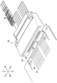
- FIG. 1 is a perspective view showing an outline of a card edge type printed wiring board and a connector connected thereto according to the present invention
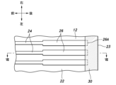
- FIG. FIG. 2 is an enlarged bottom view of a main part of the card edge type printed wiring board of the first embodiment
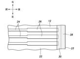
- FIG. 4 is an enlarged bottom view of a main part of the card edge type printed wiring board of Embodiment 2
- Cross-sectional view along VV in FIG. Enlarged bottom view of the main part of the card edge type printed wiring board of Embodiment 3
- Enlarged bottom view of the main part of the card edge type printed wiring board of Embodiment 4 Sectional view along VIII-VIII in FIG.
- Cross-sectional view of a main part of a card edge type printed wiring board of Embodiment 5 Enlarged bottom view of the main part of the card edge type printed wiring board of Embodiment 6
- Embodiment 1 of a card edge type printed wiring board and a card edge connector connected thereto will be described with reference to FIGS. 1 to 3.
- FIG. 1 Embodiment 1 of a card edge type printed wiring board and a card edge connector connected thereto will be described with reference to FIGS. 1 to 3.
- FIG. 1 Embodiment 1 of a card edge type printed wiring board and a card edge connector connected thereto will be described with reference to FIGS. 1 to 3.
- FIG. 1 shows a card edge type printed wiring board 10 (hereinafter abbreviated as wiring board 10) and a card edge connector 50 (abbreviated as connector 50) that is detachably attached to an edge portion 12 of the wiring board 10.
- FIG. 2 shows an enlarged bottom view of the main part of the card edge type printed wiring board 10 viewed from below.
- FIG. 3 shows a cross-sectional view along III-III in FIG.
- the wiring board 10 includes a base layer 20, an electrical insulation layer 22 laminated on one surface of the base layer 20, and a conductive pattern 24 formed on the electrical insulation layer 22.
- the base layer 20 is made of metal such as an aluminum plate, a copper plate, an iron-based metal plate, etc., having a required thickness.
- the base layer 20 preferably has a thickness of the order of 1-2 mm.
- the electrical insulating layer 22 is laminated over the entire surface of one surface of the base layer 20, and its peripheral edge reaches the edge 20A of the base layer 20 on the edge portion 12 side. As a result, the edge 20A of the electrical insulating layer 22 and the edge 22A of the electrical insulating layer 22 on the edge portion 12 side are substantially flush with each other.
- the edge 20A of the electrical insulating layer 22 and the edge 22A on the side of the edge portion 12 are collectively referred to as substrate edge 23 .
- the electrical insulating layer 22 is made of an electrically insulating resin such as polyimide or epoxy, and preferably has a uniform layer thickness of about 100 ⁇ m.
- the electrical insulating layer 22 has a hardness corresponding to a storage elastic modulus of about 1 GPa or less, and preferably has a hardness corresponding to a storage elastic modulus of 0.3 GPa or less.
- the conductive pattern 24 is made of copper foil or the like formed into a predetermined wiring pattern by etching.
- the conductive pattern 24 includes a plurality of terminal portions 26 provided for conductive contact with the connector terminals 52 of the connector 50 .
- Each terminal portion 26 forms a rectangular shape elongated in the front-rear direction (in the insertion/extraction direction with respect to the edge portion 12) in a plan view, and is arranged with a predetermined interval left and right.
- Each terminal portion 26 reaches the vicinity of the substrate edge 23 in the edge portion 12 .
- a space G1 (see FIG. 2) in the front-rear direction exists between the terminal portion 26A of the terminal portion 26 on the substrate edge 23 side and the substrate edge 23 on the electrical insulating layer 22 .
- the separation distance (gap G1) between the terminal end portion 26A of each terminal portion 26 and the substrate edge 23 is to ensure the insulation between the conductive pattern 24 and the metallic base layer 20, and It can be changed within a range in which it is possible to properly secure electrical contact with the connector terminal 52 .
- a wear-resistant layer 28 made of metal is provided on the electrical insulating layer 22 between the terminal end portion 26A of each terminal portion 26 and the substrate edge 23 .
- Each wear-resistant layer 28 is positioned with a gap G2 from the terminal portion 26A of the corresponding terminal portion 26, and extends from the edge 28A on the terminal portion 26A side of the terminal portion 26 to the substrate edge 23 in the front-rear direction. form an elongated rectangle.
- the edge 28B of the wear-resistant layer 28 on the substrate edge 23 side and the substrate edge 23 are substantially flush with each other.
- a space G2 exists between the edge 28A of the wear-resistant layer 28 and the terminal end 26A of the terminal portion 26, and sets an insulating gap for electrically separating the terminal portion 26 and the wear-resistant layer 28.
- the gap G2 is determined according to the specifications of the withstand voltage, and may preferably be about 0.2 to 0.5 mm.
- the wear resistant layer 28 is also electrically isolated from the grounded base layer 20 .
- the wear-resistant layer 28 is made of the same conductive material as the conductive pattern 24 .
- the wear-resistant layer 28 is formed together with the conductive pattern 24 by etching a copper foil or the like laminated on the base layer 20 . This eliminates the need for a separate process for providing the wear-resistant layer 28 .
- the wear-resistant layer 28 has substantially the same thickness as the conductive pattern 24 . As a result, the upper surface of the terminal portion 26 and the upper surface of the wear-resistant layer 28 are flush with each other, and the connector terminal 52 slides smoothly from the wear-resistant layer 28 to the terminal portion 26 .
- the wiring board 10 further has an electrically insulating protective layer 30 .
- the protective layer 30 continuously covers the wear-resistant layer 28, the portion of the electrical insulating layer 22 exposed to the outside at the interval G2, and the portion near the terminal portion 26A of each terminal portion 26.
- the protective layer 30 is made of a resin solder resist or the like.
- the protective layer 30 is provided in common with the plurality of terminal portions 26 and has a strip shape extending in the arrangement direction (horizontal direction) of the terminal portions 26 .
- the protective layer 30 is preferably made of a material having higher hardness than the electrical insulating layer 22 and superior wear resistance and cutting resistance to the electrical insulating layer 22 .
- the protective layer 30 tends to become thin at the portions corresponding to the edge corners (corners) C of the terminal portion 26 and the wear-resistant layer 28, as shown in FIG. There is
- the protective layer 30 may have a layer thickness of about 5 ⁇ m or more at the thinnest portion starting from the edge corner portion C. As shown in FIG.
- the protective layer 30 covers the terminal portion 26A side of the terminal portion 26 and includes a portion overlapping the terminal portion 26A side of the terminal portion 26, it is ensured that the electrical insulating layer 22 is exposed to the outside at the interval G2. Avoided. That is, the gap G2 between each wear-resistant layer 28 and the terminal portion 26A of the corresponding terminal portion 26 is filled with the protective layer 30 without fail. In addition, since the protective layer 30 includes a portion that overlaps the terminal portion 26 , separation of the terminal portion 26 ⁇ /b>A of the terminal portion 26 from the electrical insulating layer 22 is suppressed. If the protective layer 30 covers the entire terminal portion 26 , the conductive connection between the terminal portion 26 and the connector terminal 52 will be obstructed.
- the wear-resistant layer 28 and the protective layer 30 prevent the connector terminal 52 from sliding against the electrical insulating layer 22 when the connector 50 is inserted into and removed from the wiring board 10 .
- the wear-resistant layer 28 mechanically protects the electrical insulation layer 22 so as to prevent the electrical insulation layer 22 from receiving mechanical damage such as abrasion.
- the protective layer 30 mechanically double-protects the electrical insulating layer 22 together with the wear-resistant layer 28 .
- the protective layer 30 particularly prevents the electrical insulating layer 22 exposed to the outside at the gap G ⁇ b>2 from being mechanically damaged due to sliding contact with the connector terminal 52 .
- the protective layer 30 also functions as an electrical protective layer that avoids electrical short-circuiting between the wear-resistant layer 28 and other parts such as the base layer 20 .
- Embodiment 2 of the card edge type printed wiring board will be described with reference to FIGS. 4 and 5.
- FIG. 4 and 5 portions corresponding to those in FIGS. 2 and 3 are denoted by the same reference numerals as those in FIGS. 2 and 3, and description thereof will be omitted.
- each wear-resistant layer 28 extending between the terminal end portion 26A of each terminal portion 26 and the substrate edge 23 terminates with a space G3 in the front-rear direction from the substrate edge 23.
- the protective layer 30 includes a portion covering the wear-resistant layer 28 and the portion of the electrical insulating layer 22 exposed to the outside at the gap G2, and a portion covering the vicinity of the terminal portion 26A of the terminal portion 26, as well as the wear-resistant layer 28. includes a portion that covers the edge 28B (end face) on the substrate edge 23 side.
- the wear-resistant layer 28 is electrically separated from the base layer 20 by providing the gap G3 and including the portion of the protective layer 30 covering the edge 28B of the wear-resistant layer 28 on the substrate edge 23 side. becomes even more certain.
- Embodiment 3 of the card edge type printed wiring board will be described with reference to FIG. 6, portions corresponding to those in FIG. 2 are denoted by the same reference numerals as those in FIG. 2, and description thereof will be omitted.
- the protective layer 30 is omitted. Since the wear-resistant layer 28 equivalent to the wear-resistant layer 28 of the first embodiment is also provided in the third embodiment, the electrical insulating layer 22 between the end portion 26A of each terminal portion 26 and the board edge 23 is a connector. Scraping due to sliding contact of the terminal 52 is avoided. As a result, in the third embodiment as well, the occurrence of poor insulation due to scraping of the electrical insulating layer 22 and poor conduction due to shavings of the electrical insulating layer 22 is suppressed.
- Embodiment 4 of the card edge type printed wiring board will be described with reference to FIGS. 7 and 8.
- FIG. 7 and 8 portions corresponding to those in FIGS. 2 and 3 are denoted by the same reference numerals as those in FIGS. 2 and 3, and description thereof will be omitted.
- the wear-resistant layer 28 is omitted.
- a protective layer 30 equivalent to the protective layer 30 of the first embodiment is provided.
- the protective layer 30 continuously extends from the substrate edge 23 to a portion covering the terminal portion 26 in the vicinity of the terminal portion 26A.
- the protective layer 30 prevents the electrical insulating layer 22 between the end portion 26A of each terminal portion 26 and the substrate edge 23 from being scraped by the sliding contact of the connector terminal 52 .
- the occurrence of poor insulation due to scraping of the electrical insulating layer 22 and poor conduction due to shavings of the electrical insulating layer 22 is suppressed.
- Embodiment 5 of the card edge type printed wiring board will be described with reference to FIG.
- parts corresponding to those in FIG. 3 are denoted by the same reference numerals as those in FIG. 3, and description thereof will be omitted.
- the protective layer 30 covers the wear-resistant layer 28 and the entire electrical insulating layer 22 exposed to the outside at the gap G2, and the portion covering the terminal portion 26 in the vicinity of the terminal portion 26A.
- the edge 28B of the wear-resistant layer 28 on the side of the substrate edge 23 the edge 22A of the electrical insulating layer 22 on the side of the substrate edge 23, and the edge of the base layer 20 on the side of the substrate edge 23 It includes an extension 32 that continuously covers the end face of 20A.
- the extension 32 improves electrical insulation between the base layer 20 and the wear-resistant layer 28 . This more reliably prevents the wear-resistant layer 28 from becoming conductive with the base layer 20 .
- Embodiment 6 of the card edge type printed wiring board will be described with reference to FIG. 10, portions corresponding to those in FIG. 2 are denoted by the same reference numerals as those in FIG. 2, and description thereof will be omitted.
- the wear-resistant layer 28 forms a band-shaped portion extending in the arrangement direction (horizontal direction) of the plurality of terminal portions 26 and is provided in common to the plurality of terminal portions 26 .
- the wiring board 10 may be a double-sided wiring board having an electrical insulating layer 22 and conductive patterns 24 on both front and back surfaces of a base layer 20 .
- Card edge type printed wiring board (wiring board) 12 Edge portion 20 : Base layer 20A : Edge 22 : Electrical insulating layer 22A : Edge 23 : Board edge 24 : Conductive pattern 26 : Terminal portion 26A : Terminal portion 28 : Wear resistant layer 28A : Edge 28B : Edge Rim 30: Protective layer 32: Extension 50: Card edge connector (connector) 52: connector terminal
Landscapes
- Engineering & Computer Science (AREA)
- Microelectronics & Electronic Packaging (AREA)
- Manufacturing & Machinery (AREA)
- Printing Elements For Providing Electric Connections Between Printed Circuits (AREA)
Priority Applications (2)
| Application Number | Priority Date | Filing Date | Title |
|---|---|---|---|
| US18/708,035 US20250393135A1 (en) | 2021-11-08 | 2022-07-13 | Card edge type printed wiring board |
| CN202280073862.XA CN118202794A (zh) | 2021-11-08 | 2022-07-13 | 卡缘型印刷线路板 |
Applications Claiming Priority (2)
| Application Number | Priority Date | Filing Date | Title |
|---|---|---|---|
| JP2021181750A JP7834452B2 (ja) | 2021-11-08 | 2021-11-08 | カードエッジ型プリント配線基板 |
| JP2021-181750 | 2021-11-08 |
Publications (1)
| Publication Number | Publication Date |
|---|---|
| WO2023079794A1 true WO2023079794A1 (ja) | 2023-05-11 |
Family
ID=86241177
Family Applications (1)
| Application Number | Title | Priority Date | Filing Date |
|---|---|---|---|
| PCT/JP2022/027556 Ceased WO2023079794A1 (ja) | 2021-11-08 | 2022-07-13 | カードエッジ型プリント配線基板 |
Country Status (4)
| Country | Link |
|---|---|
| US (1) | US20250393135A1 (https=) |
| JP (1) | JP7834452B2 (https=) |
| CN (1) | CN118202794A (https=) |
| WO (1) | WO2023079794A1 (https=) |
Citations (8)
| Publication number | Priority date | Publication date | Assignee | Title |
|---|---|---|---|---|
| JPS5458872A (en) * | 1977-10-20 | 1979-05-11 | Nippon Telegraph & Telephone | Metallic core enclosed print plug board |
| JPS54147667U (https=) * | 1978-04-06 | 1979-10-13 | ||
| JPH07231153A (ja) * | 1994-02-15 | 1995-08-29 | Ibiden Co Ltd | カードエッジ基板 |
| JP2000113920A (ja) * | 1998-10-01 | 2000-04-21 | Mitsubishi Electric Corp | モジュール |
| JP2003142791A (ja) * | 2001-10-31 | 2003-05-16 | Fujitsu Ltd | カードエッジコネクタ及びその製造方法、電子カードならびに電子機器 |
| JP2010010600A (ja) * | 2008-06-30 | 2010-01-14 | Canon Inc | 回路基板 |
| JP2018174281A (ja) * | 2017-03-31 | 2018-11-08 | ブラザー工業株式会社 | 回路基板、液体カートリッジ及び記憶装置 |
| US20190037689A1 (en) * | 2017-12-20 | 2019-01-31 | Intel Corporation | Printed circuit board (pcb) with three-dimensional interconnects to other printed circuit boards |
Family Cites Families (1)
| Publication number | Priority date | Publication date | Assignee | Title |
|---|---|---|---|---|
| JP2007266618A (ja) | 2001-07-30 | 2007-10-11 | Seiko Epson Corp | 回路基板、及びこれを用いたインクカートリッジ、回路基板用接続装置およびこれを用いたインクジェット式記録装置 |
-
2021
- 2021-11-08 JP JP2021181750A patent/JP7834452B2/ja active Active
-
2022
- 2022-07-13 US US18/708,035 patent/US20250393135A1/en active Pending
- 2022-07-13 WO PCT/JP2022/027556 patent/WO2023079794A1/ja not_active Ceased
- 2022-07-13 CN CN202280073862.XA patent/CN118202794A/zh active Pending
Patent Citations (8)
| Publication number | Priority date | Publication date | Assignee | Title |
|---|---|---|---|---|
| JPS5458872A (en) * | 1977-10-20 | 1979-05-11 | Nippon Telegraph & Telephone | Metallic core enclosed print plug board |
| JPS54147667U (https=) * | 1978-04-06 | 1979-10-13 | ||
| JPH07231153A (ja) * | 1994-02-15 | 1995-08-29 | Ibiden Co Ltd | カードエッジ基板 |
| JP2000113920A (ja) * | 1998-10-01 | 2000-04-21 | Mitsubishi Electric Corp | モジュール |
| JP2003142791A (ja) * | 2001-10-31 | 2003-05-16 | Fujitsu Ltd | カードエッジコネクタ及びその製造方法、電子カードならびに電子機器 |
| JP2010010600A (ja) * | 2008-06-30 | 2010-01-14 | Canon Inc | 回路基板 |
| JP2018174281A (ja) * | 2017-03-31 | 2018-11-08 | ブラザー工業株式会社 | 回路基板、液体カートリッジ及び記憶装置 |
| US20190037689A1 (en) * | 2017-12-20 | 2019-01-31 | Intel Corporation | Printed circuit board (pcb) with three-dimensional interconnects to other printed circuit boards |
Also Published As
| Publication number | Publication date |
|---|---|
| JP7834452B2 (ja) | 2026-03-24 |
| CN118202794A (zh) | 2024-06-14 |
| US20250393135A1 (en) | 2025-12-25 |
| JP2023069689A (ja) | 2023-05-18 |
Similar Documents
| Publication | Publication Date | Title |
|---|---|---|
| JP5818516B2 (ja) | コネクタ接続部を有するフレキシブルプリント配線基板 | |
| US20120129404A1 (en) | Communication Jack Having Layered Plug Interface Contacts | |
| US8708712B2 (en) | Male connector block, female connector block, and connector | |
| US20140293559A1 (en) | Wiring board | |
| WO2023079794A1 (ja) | カードエッジ型プリント配線基板 | |
| US10020441B2 (en) | Piezoelectric transformer device | |
| JP4363664B1 (ja) | フレキシブルフラットケーブル | |
| KR20220098736A (ko) | 배선 회로 기판 및 그 제조 방법 | |
| US12363821B2 (en) | Circuit module | |
| CN221306164U (zh) | 多层基板以及电子设备 | |
| CN113924213A (zh) | 热敏打印头 | |
| JP2000261109A (ja) | 配線基板 | |
| US7126057B2 (en) | Integrated electronic component | |
| JP7123236B2 (ja) | 回路基板 | |
| JP4721926B2 (ja) | 多数個取り配線基板 | |
| JP7817459B2 (ja) | 印刷配線板 | |
| US20250071900A1 (en) | Circuit body and connector-attached circuit body | |
| TWI910120B (zh) | 配線電路基板 | |
| JP2021068829A (ja) | 配線基板 | |
| US12446193B2 (en) | Heat-dissipating structure | |
| JP7657543B2 (ja) | 配線回路基板およびその製造方法 | |
| JPH066006A (ja) | 部品端子の接続構造 | |
| JP2006040967A (ja) | 多層フレキシブルプリント基板およびこれを用いた圧接接続構造 | |
| WO2024203720A1 (ja) | 配線基板 | |
| KR20240133588A (ko) | 배선 회로 기판 |
Legal Events
| Date | Code | Title | Description |
|---|---|---|---|
| 121 | Ep: the epo has been informed by wipo that ep was designated in this application |
Ref document number: 22889619 Country of ref document: EP Kind code of ref document: A1 |
|
| WWE | Wipo information: entry into national phase |
Ref document number: 202280073862.X Country of ref document: CN |
|
| WWE | Wipo information: entry into national phase |
Ref document number: 2401002913 Country of ref document: TH |
|
| WWE | Wipo information: entry into national phase |
Ref document number: 202447043522 Country of ref document: IN |
|
| 122 | Ep: pct application non-entry in european phase |
Ref document number: 22889619 Country of ref document: EP Kind code of ref document: A1 |