WO2023079648A1 - Dispositif d'irradiation laser, procédé d'irradiation laser et procédé de fabrication d'un dispositif d'affichage - Google Patents
Dispositif d'irradiation laser, procédé d'irradiation laser et procédé de fabrication d'un dispositif d'affichage Download PDFInfo
- Publication number
- WO2023079648A1 WO2023079648A1 PCT/JP2021/040657 JP2021040657W WO2023079648A1 WO 2023079648 A1 WO2023079648 A1 WO 2023079648A1 JP 2021040657 W JP2021040657 W JP 2021040657W WO 2023079648 A1 WO2023079648 A1 WO 2023079648A1
- Authority
- WO
- WIPO (PCT)
- Prior art keywords
- laser light
- substrate
- laser
- irradiation
- optical system
- Prior art date
Links
- 238000000034 method Methods 0.000 title claims description 62
- 238000004519 manufacturing process Methods 0.000 title claims description 34
- 239000000758 substrate Substances 0.000 claims abstract description 146
- 230000003287 optical effect Effects 0.000 claims abstract description 107
- 238000007667 floating Methods 0.000 claims abstract description 29
- 230000007246 mechanism Effects 0.000 claims description 53
- 230000032258 transport Effects 0.000 claims description 51
- 239000004065 semiconductor Substances 0.000 claims description 44
- 238000005339 levitation Methods 0.000 claims description 32
- 238000002425 crystallisation Methods 0.000 claims description 26
- 230000008025 crystallization Effects 0.000 claims description 26
- 230000001678 irradiating effect Effects 0.000 claims description 25
- 238000007493 shaping process Methods 0.000 claims description 15
- 230000008859 change Effects 0.000 claims description 11
- 239000010408 film Substances 0.000 description 140
- 229910021417 amorphous silicon Inorganic materials 0.000 description 24
- 230000008569 process Effects 0.000 description 21
- XUIMIQQOPSSXEZ-UHFFFAOYSA-N Silicon Chemical compound [Si] XUIMIQQOPSSXEZ-UHFFFAOYSA-N 0.000 description 20
- 229910052710 silicon Inorganic materials 0.000 description 20
- 239000010703 silicon Substances 0.000 description 20
- 238000000137 annealing Methods 0.000 description 19
- 230000035515 penetration Effects 0.000 description 16
- 239000010410 layer Substances 0.000 description 14
- 238000006356 dehydrogenation reaction Methods 0.000 description 13
- 229910021420 polycrystalline silicon Inorganic materials 0.000 description 12
- 229920005591 polysilicon Polymers 0.000 description 12
- UFHFLCQGNIYNRP-UHFFFAOYSA-N Hydrogen Chemical compound [H][H] UFHFLCQGNIYNRP-UHFFFAOYSA-N 0.000 description 8
- 239000001257 hydrogen Substances 0.000 description 8
- 229910052739 hydrogen Inorganic materials 0.000 description 8
- 239000000463 material Substances 0.000 description 7
- 239000012044 organic layer Substances 0.000 description 7
- 239000007789 gas Substances 0.000 description 6
- 239000011521 glass Substances 0.000 description 5
- 230000004048 modification Effects 0.000 description 5
- 238000012986 modification Methods 0.000 description 5
- 239000013307 optical fiber Substances 0.000 description 5
- 238000005224 laser annealing Methods 0.000 description 4
- 238000007789 sealing Methods 0.000 description 4
- 239000010409 thin film Substances 0.000 description 4
- 238000010521 absorption reaction Methods 0.000 description 3
- 238000001816 cooling Methods 0.000 description 3
- 238000006073 displacement reaction Methods 0.000 description 3
- 238000010438 heat treatment Methods 0.000 description 3
- 239000011148 porous material Substances 0.000 description 3
- 239000011347 resin Substances 0.000 description 3
- 229920005989 resin Polymers 0.000 description 3
- 238000001004 secondary ion mass spectrometry Methods 0.000 description 3
- 239000004696 Poly ether ether ketone Substances 0.000 description 2
- 230000008033 biological extinction Effects 0.000 description 2
- 238000005229 chemical vapour deposition Methods 0.000 description 2
- 239000011159 matrix material Substances 0.000 description 2
- 239000012528 membrane Substances 0.000 description 2
- 229910052751 metal Inorganic materials 0.000 description 2
- 239000002184 metal Substances 0.000 description 2
- 239000007769 metal material Substances 0.000 description 2
- 229920002530 polyetherether ketone Polymers 0.000 description 2
- 230000003746 surface roughness Effects 0.000 description 2
- 229910000838 Al alloy Inorganic materials 0.000 description 1
- RYGMFSIKBFXOCR-UHFFFAOYSA-N Copper Chemical compound [Cu] RYGMFSIKBFXOCR-UHFFFAOYSA-N 0.000 description 1
- VYPSYNLAJGMNEJ-UHFFFAOYSA-N Silicium dioxide Chemical compound O=[Si]=O VYPSYNLAJGMNEJ-UHFFFAOYSA-N 0.000 description 1
- 229910052782 aluminium Inorganic materials 0.000 description 1
- XAGFODPZIPBFFR-UHFFFAOYSA-N aluminium Chemical compound [Al] XAGFODPZIPBFFR-UHFFFAOYSA-N 0.000 description 1
- PNEYBMLMFCGWSK-UHFFFAOYSA-N aluminium oxide Inorganic materials [O-2].[O-2].[O-2].[Al+3].[Al+3] PNEYBMLMFCGWSK-UHFFFAOYSA-N 0.000 description 1
- 229910010293 ceramic material Inorganic materials 0.000 description 1
- 229910052802 copper Inorganic materials 0.000 description 1
- 239000010949 copper Substances 0.000 description 1
- 229910021419 crystalline silicon Inorganic materials 0.000 description 1
- 230000007423 decrease Effects 0.000 description 1
- 230000001419 dependent effect Effects 0.000 description 1
- 230000006866 deterioration Effects 0.000 description 1
- 238000010586 diagram Methods 0.000 description 1
- 238000009792 diffusion process Methods 0.000 description 1
- 230000000694 effects Effects 0.000 description 1
- 238000005401 electroluminescence Methods 0.000 description 1
- 230000017525 heat dissipation Effects 0.000 description 1
- 238000005286 illumination Methods 0.000 description 1
- 238000005499 laser crystallization Methods 0.000 description 1
- 229910021424 microcrystalline silicon Inorganic materials 0.000 description 1
- 229910021421 monocrystalline silicon Inorganic materials 0.000 description 1
- 238000005192 partition Methods 0.000 description 1
- 230000009467 reduction Effects 0.000 description 1
- 229910052814 silicon oxide Inorganic materials 0.000 description 1
- 238000009751 slip forming Methods 0.000 description 1
- 238000001179 sorption measurement Methods 0.000 description 1
- XLYOFNOQVPJJNP-UHFFFAOYSA-N water Substances O XLYOFNOQVPJJNP-UHFFFAOYSA-N 0.000 description 1
Images


Classifications
-
- H—ELECTRICITY
- H01—ELECTRIC ELEMENTS
- H01L—SEMICONDUCTOR DEVICES NOT COVERED BY CLASS H10
- H01L21/00—Processes or apparatus adapted for the manufacture or treatment of semiconductor or solid state devices or of parts thereof
- H01L21/02—Manufacture or treatment of semiconductor devices or of parts thereof
- H01L21/04—Manufacture or treatment of semiconductor devices or of parts thereof the devices having at least one potential-jump barrier or surface barrier, e.g. PN junction, depletion layer or carrier concentration layer
- H01L21/18—Manufacture or treatment of semiconductor devices or of parts thereof the devices having at least one potential-jump barrier or surface barrier, e.g. PN junction, depletion layer or carrier concentration layer the devices having semiconductor bodies comprising elements of Group IV of the Periodic System or AIIIBV compounds with or without impurities, e.g. doping materials
- H01L21/26—Bombardment with radiation
- H01L21/263—Bombardment with radiation with high-energy radiation
- H01L21/268—Bombardment with radiation with high-energy radiation using electromagnetic radiation, e.g. laser radiation
Definitions
- the present invention relates to a laser irradiation device, a laser irradiation method, and a display manufacturing method.
- Patent Document 1 discloses a laser annealing apparatus using an excimer laser.
- the transport unit transports the substrate while the floating unit floats the substrate. Then, the substrate being transported is irradiated with the line-shaped laser beam.
- the laser irradiation device is a laser irradiation device that irradiates a film provided on a substrate with a laser beam, and is a laser light source that generates a laser beam having a wavelength at least part of which is transmitted through the film. and an optical system unit that guides the laser beam to the substrate, and a levitation unit that has a through hole provided immediately below the irradiation position of the laser beam and floats the substrate.
- a laser irradiation apparatus includes a semiconductor laser light source that generates a laser beam having a wavelength of 500 nm or less, a transport unit that transports a substrate in a first direction, and a pulsed laser beam that emits the laser beam to the substrate. and a driving mechanism for driving the optical system unit so as to change the irradiation position of the laser beam with respect to the substrate in a second direction different from the first direction when viewed from above.
- the laser irradiation device is a laser irradiation device that dehydrogenates a film provided on a substrate, and includes a semiconductor laser light source that generates a laser beam having a wavelength of 500 nm or less; An optical system unit that guides a laser beam to a substrate and a drive mechanism that changes the irradiation position of the laser beam on the substrate are provided.
- a laser irradiation apparatus includes a transport unit that generates a substrate on which a film is formed in a first direction, a semiconductor laser light source that generates a laser beam with a wavelength of 500 nm or less, and a substrate that emits the laser beam. a driving mechanism for changing the irradiation position of the laser beam with respect to the substrate in a second direction inclined from the first direction when viewed from above; and an excimer laser for crystallizing the film.
- an excimer laser light source that generates light; and an optical system for crystallization that guides the excimer laser light to the substrate being transported as a linear line beam having a longitudinal direction inclined from the first direction when viewed from above. and have.
- the laser irradiation method is a laser irradiation method for irradiating a film provided on a substrate with a laser beam, comprising: (A1) a through hole provided immediately below the laser beam irradiation position; (A2) generating a laser beam having a wavelength at least a portion of which is transmitted through the film; leading to the substrate.
- the laser irradiation method includes the steps of (B1) generating laser light with a wavelength of 500 nm or less using a semiconductor laser light source, and (B2) transporting the substrate in a first direction by a transport unit. (B3) guiding the laser light, which is a pulsed light, to the substrate by an optical system unit; and (B4) irradiating the substrate with the laser light in a second direction different from the first direction when viewed from above. and C. driving the optics unit to change position.
- the laser irradiation method is a laser irradiation method for performing a dehydrogenation treatment on a film provided on a substrate, and (C1) emits a laser beam having a wavelength of 500 nm or less from a semiconductor laser light source. (C2) guiding the laser light to the substrate by an optical system unit; and (C3) changing the irradiation position of the laser light on the substrate.
- the laser irradiation method comprises the steps of: (D1) transporting a substrate having a film formed thereon in a first direction by a transport unit; (D3) guiding the laser beam to the substrate by an optical system unit; (D5) generating an excimer laser beam for crystallizing the film from an excimer laser light source; (D6) directing the excimer laser beam in the first direction when viewed from above; and guiding the light beam to the substrate being transported as a line-shaped line beam whose longitudinal direction is the direction inclined from the vertical direction.
- the display manufacturing method includes (S1) an irradiation step of irradiating a film formed on a substrate with a laser beam, and the (S1) irradiation step includes (SA1) the irradiation of the laser beam.
- SA2 generating a laser beam having a wavelength at least partially transmitted through the film;
- SA3 optical and guiding the laser light to the floating substrate by a system unit.
- the display manufacturing method includes (S1) an irradiation step of irradiating a film formed on a substrate with laser light, and the (S1) irradiation step includes (SB1) a semiconductor laser light source.
- (SB2) transporting a substrate in a first direction by a transport unit; and (SB3) guiding the laser beam, which is pulsed light, to the substrate by an optical system unit.
- (SB4) driving the optical system unit so as to change the irradiation position of the laser light on the substrate in a second direction different from the first direction when viewed from above.
- the display manufacturing method includes (T1) an irradiation step of irradiating the film formed on the substrate with a laser beam in order to dehydrogenate the film, and the ( T1)
- the irradiating step includes (TC1) generating laser light with a wavelength of 500 nm or less from a semiconductor laser light source, (TC2) guiding the laser light to a substrate by an optical system unit, and (TC3) and changing the irradiation position of the laser light.
- the display manufacturing method includes (S1) an irradiation step of irradiating a film formed on a substrate with a laser beam, and the (S1) irradiation step includes (SD1) a transport unit, (SD2) generating a laser beam with a wavelength of 500 nm or less using a semiconductor laser light source; (SD4) changing the irradiation position of the laser beam with respect to the substrate in a second direction different from the first direction when viewed from the top; (SD5) exposing the film to the (SD6) generating an excimer laser beam for crystallization; and (SD6) the excimer laser beam being transported as a line-shaped line beam having a longitudinal direction inclined from the first direction when viewed from above. leading to the substrate.
- SD1 a transport unit
- SD2 generating a laser beam with a wavelength of 500 nm or less using a semiconductor laser light source
- SD4 changing the irradiation position of the laser beam with respect to the substrate in a second direction different from the first direction when
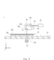
- FIG. 1 is a top view schematically showing a laser irradiation device according to an embodiment
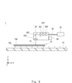
- FIG. 1 is an XZ sectional view schematically showing a laser irradiation device according to an embodiment
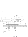
- FIG. 1 is a YZ sectional view schematically showing a laser irradiation device according to an embodiment
- FIG. 4 is a table showing the penetration depth of silicon membranes
- It is an XZ sectional view which shows typically the laser irradiation apparatus concerning a modification.
- FIG. 3 is a side view schematically showing a laser irradiation device according to a second embodiment
- FIG. It is a top view which shows the spot shape of a laser beam typically.
- FIG. 1 is a top view schematically showing a laser irradiation device according to an embodiment
- FIG. 1 is an XZ sectional view schematically showing a laser irradiation device according to an embodiment
- FIG. 1 is a YZ sectional view schematically showing a laser i
- FIG. 11 is a top view schematically showing a laser irradiation device according to a third embodiment;
- FIG. 11 is a side view schematically showing a laser irradiation device according to a third embodiment;
- 4 is a photograph showing an annealed silicon film;
- FIG. 4 is a SIMS profile showing hydrogen concentration in an annealed silicon film;
- FIG. 1 is a cross-sectional view showing a simplified configuration of an organic EL display;
- FIG. It is process sectional drawing which shows the manufacturing method of the display concerning this Embodiment. It is process sectional drawing which shows the manufacturing method of the display concerning this Embodiment.
- the laser irradiation apparatus performs annealing by irradiating an object to be processed (also referred to as a work) with a laser beam.
- the laser irradiation apparatus heats the substrate with laser light to perform dehydrogenation annealing treatment on a film provided on the substrate.
- the object to be processed is a film-coated substrate on which a silicon film is formed.
- the laser irradiation device uses a blue semiconductor laser light source as a laser light source.
- the laser irradiation device irradiates the object to be processed with a blue laser beam from a semiconductor laser light source, thereby performing a dehydrogenation process on the silicon film.
- Laser light is not limited to blue laser light, and laser light with a wavelength of 500 nm or less can be used.
- a film forming device forms a film on a substrate. Then, a laser irradiation device irradiates the film with a laser beam.
- the substrate is, for example, a transparent substrate such as a glass substrate or a resin substrate, and the film is, for example, an amorphous silicon film.
- a substrate with an amorphous silicon film is an object to be processed.
- the laser irradiation device dehydrogenates the amorphous silicon film by irradiating the amorphous silicon film with laser light.
- the object to be processed may be a film-coated substrate on which a film other than a silicon film is formed.
- the laser irradiation apparatus is a dehydrogenation annealing apparatus using laser light, but it may be a crystallization annealing apparatus for crystallizing an amorphous silicon film by laser irradiation.
- FIG. 1 is a top view schematically showing the configuration of a laser irradiation device 1.
- FIG. 2 is an XZ sectional view schematically showing the configuration of the laser irradiation device 1.
- FIG. 3 is a YZ cross-sectional view schematically showing the configuration of the laser irradiation device 1. As shown in FIG.
- the laser irradiation device 1 includes a levitation unit 10, a transport unit 11, an optical system unit 30, a Y driving mechanism 32, and a stage 40.
- the levitation unit 10 and the transport unit 11 constitute a transport device.
- the diagrams shown below show an XYZ three-dimensional orthogonal coordinate system as appropriate for simplification of explanation.
- the Z direction is a vertical up-down direction, and is a direction perpendicular to the main surface of the object 16 to be processed.
- the X direction is the transport direction of the object 16 to be processed.
- the Y direction is the moving direction of the optical system unit 30 .
- a laser beam 15 is applied to an object 16 being transported in the X direction.
- the optical system unit 30 moves in the Y direction. Therefore, the irradiation position of the laser beam on the object to be processed 16 can be changed in the X direction and the Y direction. As a result, substantially the entire surface of the object 16 to be processed can be irradiated with the laser beam.
- the levitation unit 10 is configured to eject gas from the surface of the levitation unit 10 .
- the levitation unit 10 levitates the object 16 to be processed on its upper surface.
- the gas ejected from the surface of the floating unit 10 is sprayed onto the lower surface of the object 16 to float, thereby causing the object 16 to float.
- the floating unit 10 adjusts the floating amount so that the object 16 to be processed does not come into contact with another mechanism (not shown) arranged above the object 16 to be processed.
- the floating unit 10 is made of a porous material.
- the floating unit 10 is made of a ceramic material such as porous alumina or porous SiC.
- the levitation unit 10 is a porous material plate with a thickness of 10 mm.
- the floating unit 10 is connected to an air supply port (not shown). Therefore, gas from a gas supply means (not shown) such as a gas cylinder is jetted out from the upper surface of the levitation unit 10 .
- the transport unit 11 transports the floating object to be processed 16 in the transport direction.
- the transport unit 11 has a holding mechanism 12 and a moving mechanism 13 .
- the holding mechanism 12 holds the object 16 to be processed.
- the holding mechanism 12 can be configured using a vacuum suction mechanism.
- the vacuum adsorption mechanism is made of metal material such as aluminum alloy.
- the holding mechanism 12 may be made of a resin-based material such as PEEK (polyetheretherketone) material.
- a suction groove, a suction hole, and the like are formed on the upper surface of the holding mechanism 12 .
- the holding mechanism 12 may be made of a porous material.
- the holding mechanism 12 vacuum suction mechanism
- the holding mechanism 12 is connected to an exhaust port (not shown), and the exhaust port is connected to an ejector, a vacuum pump, and the like. Therefore, since a negative pressure for sucking gas acts on the holding mechanism 12 , the object to be processed 16 can be held using the holding mechanism 12 .
- the holding mechanism 12 sucks the surface (lower surface) of the object 16 to be processed that is opposite to the surface (upper surface) irradiated with the laser beam 15 , that is, the surface of the object 16 to be processed that faces the levitation unit 10 . and holds the object 16 to be processed. In addition, the holding mechanism 12 holds the +Y-direction end of the object 16 to be processed.
- a moving mechanism 13 provided in the transport unit 11 is connected to the holding mechanism 12 .
- the moving mechanism 13 is configured to move the holding mechanism 12 in the transport direction.
- the transport unit 11 (holding mechanism 12 and moving mechanism 13) is provided on the +Y-direction end side of the levitation unit 10. While the holding mechanism 12 holds the object to be processed 16, the moving mechanism 13 moves in the transport direction.
- the object to be processed 16 is conveyed by moving.
- the moving mechanism 13 is configured to slide the end of the levitation unit 10 in the +Y direction along the transport direction.
- the moving mechanism 13 slides the end of the levitation unit 10 along the transport direction, thereby transporting the workpiece 16 along the transport direction.
- the moving mechanism 13 includes, for example, an actuator such as a motor (not shown), a linear guide mechanism, an air bearing, and the like.
- the object 16 to be processed is a rectangular substrate having edges parallel to the X direction and the Y direction.
- the object 16 to be processed includes a substrate 16a and a film 16b formed on the substrate 16a.
- the substrate 16a is a transparent substrate such as a glass substrate.
- Film 16b is a silicon film, such as an amorphous silicon film. By irradiating the film 16b with the laser light 15 for annealing, hydrogen contained in the film 16b can be removed. That is, the laser irradiation device 1 serves as a dehydrogenation device.
- the film 16b which is a silicon film, is shown, other films may be formed.
- a thin film of copper or aluminum that serves as wiring may be formed as a base film of the silicon film.
- an insulating film such as a silicon oxide film may be formed on the substrate 16a as a base film.
- a stage 40 is arranged above the levitation unit 10 .
- the stage 40 movably holds the optical system unit 30 .
- the optical system unit 30 guides the laser light from the laser light source 35 to the object 16 to be processed.
- the optical system unit 30 is arranged on the ⁇ X side of the stage 40 . Therefore, the optical system unit 30 is arranged directly above the object 16 to be processed. Therefore, the object to be processed 16 is irradiated with the laser beam 15 from the optical system unit 30 from above.
- the stage 40 serves as a guide mechanism that guides the movement of the optical system unit 30 in the Y direction.
- the stage 40 is provided with guide rails, guide grooves, and the like.
- a Y drive mechanism 32 is also provided on the stage 40 .
- the stage 40 is a gantry stage provided along the Y direction in the space above the levitation unit 10 .
- a Y drive mechanism 32 drives the optical system unit 30 in the Y direction.
- the optical system unit 30 moves along the stage 40. Since the optical system unit 30 moves in the Y direction, the irradiation position of the laser beam 15 changes in the Y direction.
- the stage 40 is arranged to protrude from the levitation unit 10 on the +Y side and the -Y side. Therefore, in the Y direction, the optical system unit 30 can irradiate laser light to any position on the object 16 to be processed.
- the laser light source 35 generates laser light for annealing the object 16 to be processed.
- the laser light source 35 is a BLD (Blue Laser Diode) that generates blue laser light with a central wavelength of 450 nm. That is, the laser light source 35 is a blue semiconductor laser light source.
- the laser light is a continuous wave (CW) laser light.
- the laser irradiation device 1 may use a modulator or the like to modulate the laser light into a pulsed laser light.
- a laser light source 35 is coupled to an optical fiber 36 .
- Laser light from the laser light source 35 enters the optical system unit 30 via the optical fiber 36 .
- the optical system unit 30 has a lens 301, a mirror 302, and a lens 303.
- the optical system unit 30 may be provided with optical elements other than the lens 301 , the mirror 302 and the lens 303 .
- the spot shape of the laser beam 15 is a line shape of 10 mm ⁇ 0.3 mm.
- the laser light 15 is CW light, and the irradiation time at one point on the object 16 to be processed is set to 10 ⁇ sec to 1 sec.
- a laser beam from the optical fiber 36 enters the lens 301 .
- a laser beam condensed by the lens 301 is incident on the mirror 302 .
- the mirror 302 reflects the laser light toward the object 16 to be processed. Specifically, the mirror 302 reflects the laser light downward.
- the laser beam reflected by the mirror 302 enters the lens 303 .
- the object 16 to be processed is irradiated with the laser beam 15 from the lens 303 .
- the lens 303 converges the laser beam 15 onto the object 16 to be processed. Therefore, the laser beam 15 from the optical system unit 30 becomes a converging beam and is irradiated onto the object 16 to be processed.
- the optical system unit 30 irradiates the object 16 to be processed with the laser beam 15 from above.
- the film 16b of the object 16 to be processed is annealed, and dehydrogenation treatment can be performed on the film 16b.
- the optical axis of the lens 303 is parallel to the Z direction, it may be tilted from the Z direction.
- the laser light source 35 is a blue semiconductor laser light source
- the laser light 15 is blue laser light.
- the center wavelength of the laser light 15 is 450 nm. Blue light has a deep penetration depth into the silicon film. Therefore, not all of the laser beam 15 is absorbed by the object 16 to be processed, and part of the laser beam 15 is transmitted through the object 16 to be processed.
- the levitation unit 10 is heated. Therefore, the temperature of the levitation unit 10 fluctuates during the process. Furthermore, since the laser light is reflected or scattered on the surface of the levitation unit 10 , the laser light from directly below the irradiated portion enters the object 16 to be processed again. Therefore, the annealing process for dehydrogenation may become unstable.
- the levitation unit 10 is provided with a through hole 10a directly below the irradiation location of the laser beam 15.
- FIG. When viewed from above, the through hole 10a is formed in a belt-like region having the Y direction as the longitudinal direction.
- the laser beam 15 does not enter the levitation unit 10 because it passes through the through hole 10a. Absorption, reflection or scattering of the laser light 15 in the levitation unit 10 can be prevented.
- the width of the through hole 10a in the X direction is about 10 mm.
- the length of the through hole 10 a in the Y direction is approximately the same as the movable range of the optical system unit 30 .
- the temperature of the levitation unit 10 can be stabilized. Furthermore, it is possible to prevent reflected light or scattered light from the floating unit 10 from entering the object 16 again. Reflected light and scattered light from the surface of the levitation unit 10 can be reduced. By doing so, a stable dehydrogenation process becomes possible, and productivity can be improved.
- the Y drive mechanism 32 drives the optical system unit 30 while the transport unit 11 transports the object 16 to be processed. That is, the Y drive mechanism 32 moves the irradiation position of the laser beam in the Y direction, and the transport unit 11 moves the object 16 to be processed in the X direction. Therefore, the irradiation position of the laser beam on the object to be processed 16 changes in the X direction and the Y direction. As a result, substantially the entire surface of the object 16 to be processed can be irradiated with the laser beam. Therefore, almost the entire film 16b can be annealed, and the dehydrogenation treatment can be appropriately performed.
- the moving speed of the optical system unit 30 in the Y direction may be faster than the transport speed in the X direction.
- the laser irradiation position can be changed at high speed in the Y direction. Therefore, since local heating can be prevented, an influence on a base film or the like can be prevented.
- the laser light source 35 is not limited to this. Specifically, when a film 16b having a predetermined thickness is provided on the substrate 16a, the laser light source 35 may generate laser light having a wavelength that at least part of the laser light passes through the film 16b. Just do it.
- the penetration depth (penetration depth) for light with a wavelength of 450 nm is 0.02 ⁇ m.
- the penetration depth is the thickness of a material when the amount of light incident on the material becomes 1/e. e is the Napier number.
- the penetration depth is determined by the material's extinction coefficient. Also, the extinction coefficient is wavelength dependent. The depth of penetration is determined by the material of the membrane and the wavelength of the light.
- FIG. 4 is a table showing penetration depths of an amorphous silicon (a-Si) film and a single crystal silicon (c-Si) film.
- FIG. 4 shows the penetration depth for light with wavelengths of 308 nm, 355 nm, 450 nm, 532 nm and 808 nm.
- the penetration depth is the film thickness when the absorptance becomes 1/e (63%). If the film 16b is an amorphous silicon film and the laser wavelength is 450 nm, the penetration depth is 0.02 ⁇ m.
- the laser irradiation apparatus 1 is suitable for annealing the film 16b having a film thickness of four times or less the penetration depth. In other words, when annealing a film having a film thickness greater than four times the penetration depth, the effect on the levitation unit 10 is minor. If the thickness of the film 16b is determined, the range of laser wavelength suitable for this embodiment is determined.
- the film 16b is an amorphous silicon film with a thickness of 40 nm.
- the penetration depth is 10 nm when the laser wavelength is 355 nm.
- the laser wavelength is 355 nm or more
- 2% or more of the laser light is transmitted through the film 16b, which affects the process.
- 2% or more of the laser light passes through the film 16b.
- Absorption, reflection, or scattering at the levitation unit 10 can cause process variations.
- the laser irradiation apparatus is suitable when laser light with a wavelength of 355 nm or more and 808 nm or less is used. That is, it is suitable for annealing a film having a film thickness four times or less the penetration depth of light of a laser wavelength.
- the optical system unit 30 may have an optical scanner for scanning laser light.
- mirror 302 may be a galvanometric mirror.
- the optical scanner changes the irradiation position of the laser light by deflecting the laser light.
- the optical scanner is a uniaxial optical scanner that changes the irradiation position of the laser light in the X direction. That is, by changing the irradiation position of the optical scanner in the X direction, it is possible to shorten the irradiation time during which one point of the object 16 to be processed is continuously irradiated with the laser beam. This can prevent local heating of the base film or the like. Therefore, a stable annealing process becomes possible.
- lens 303 may be an f-theta lens. Thereby, even when the optical scanner deflects the laser light, the irradiation direction of the laser light can be made parallel to the Z direction.
- a laser irradiation method is a laser irradiation method for irradiating a film provided on a substrate with laser light.
- the laser irradiation method comprises the steps of: floating the substrate by a floating unit having a through hole provided immediately below a laser beam irradiation position; and transporting the substrate floating on the floating unit in a first direction. generating a laser beam having a wavelength at least part of which is transmitted through the film; guiding the laser beam to the substrate being transported by an optical system unit; and moving the optical system unit in a second direction so as to change the irradiation position of the laser light in a second direction different from the above.
- productivity can be improved.
- FIG. 5 is a side sectional view schematically showing the configuration of the laser irradiation device 1. As shown in FIG. In modification 1, a damper 19 is added to the configuration of the first embodiment.
- the damper 19 is arranged directly below the through hole 10a.
- the damper 19 absorbs the laser beam 15 that has passed through the through hole 10a.
- the damper 19 is a metal block whose longitudinal direction is the Y direction. The length can be approximately the same as that of the through hole 10a.
- the damper 19 is made of a metallic material or the like colored black.
- the damper 19 is arranged directly below the through-hole 10a in FIG. 5, the arrangement location of the damper 19 is not limited to directly below the through-hole 10a.
- a mirror or the like that reflects the blue laser light may be arranged directly below the through hole 10a.
- the damper 19 may be arranged at a position where it can absorb the laser beam reflected by the mirror. That is, the damper 19 absorbs the blue laser light reflected by the mirror.
- the damper 19 may be cooled.
- the damper 19 may be provided with a cooling mechanism such as an air cooling mechanism or a water cooling mechanism.
- the damper 19 may be provided with a heat dissipation mechanism. By doing so, the temperature rise of the damper 19 and its surroundings can be suppressed, so that the annealing process can be performed stably.
- FIG. 6 is a cross-sectional view schematically showing the configuration of the laser irradiation device 1.
- the laser irradiation device 1 is a laser crystallization device for crystallizing an amorphous silicon film.
- the film 16b before laser light irradiation is an amorphous silicon film.
- the film 16b after laser light irradiation is a polysilicon film.
- a laser light source 35 is a blue semiconductor laser light source. By irradiating the blue laser light, the film 16b becomes a polysilicon film.
- the laser irradiation device 1 has a modulator 306 and a beam shaping section 307 .
- the modulator 306 and beam shaping section 307 are mounted on the optical system unit 30 . Configurations other than the modulator 306 and the beam shaping section 307 are the same as those in the first embodiment, so description thereof will be omitted.
- a modulator 306 modulates the laser light. This modulates the CW laser light into pulsed laser light.
- the repetition frequency R of the pulsed laser light is 10 kHz to 200 kHz. It is preferable that the irradiation time during which the laser beam is continuously irradiated to one location of the object 16 to be processed is 1 ⁇ sec or less.
- the pulsed laser light from the modulator 306 enters the beam shaping section 307 .
- a beam shaping section 307 shapes the spot shape of the pulsed laser light.
- the beam shaping section 307 has a beam shaping mechanism such as a slit.
- the beam may be shaped by the placement of the output ends of the optical fibers 36 .
- the beam shaping section 307 shapes the beam so that the beam cross-sectional shape (spot shape) in the direction perpendicular to the optical axis is rectangular.
- the shape of the spot is rectangular with a size of 10 mm in the longitudinal direction and a size of 0.03 mm in the lateral direction.
- the spot shape of the beam on the object to be processed 16 will be described later.
- the pulsed laser light shaped by the beam shaping unit 307 is incident on the object to be processed 16 via the lens 301, the mirror 302 and the lens 303, as in the first embodiment.
- FIG. 7 shows the beam spot shape on the object 16 to be processed.
- FIG. 7 is an XY plan view schematically showing the spot shape of the pulsed laser beam on the object 16 to be processed.
- the transportation speed of the object to be processed 16 by the transportation unit 11 is sufficiently slower than the moving speed of the optical system unit 30 by the Y drive mechanism 32 .
- the sizes and the like shown below are examples of the present embodiment, and the present embodiment is not limited to the following sizes.
- the shape of the spot of the laser beam 15 on the object 16 to be processed is rectangular with a longitudinal direction.
- the size L of the spot shape in the longitudinal direction is 900 ⁇ m
- the size in the lateral direction is 15 ⁇ m.
- the lateral direction and the longitudinal direction are directions orthogonal to each other.
- the longitudinal direction is inclined from the X direction and the Y direction. Specifically, the angle ⁇ between the lateral direction and the Y direction is 45°. That is, the longitudinal direction of the spot shape is slanted by 45° from the moving direction of the optical system unit 30 .
- the moving speed V of the optical system unit 30 in the Y direction is 70.7 mm/s.
- the beam edge has a lower light intensity than the beam center. That is, the light intensity is highest at the center of the beam, and the light intensity decreases from the center of the beam toward the ends of the beam.
- the beam end portion with low light intensity is repeatedly irradiated many times, the surface roughness of the film 16b will differ from that of the other portions. Therefore, display unevenness occurs in the display.
- the longitudinal direction of the beam cross section is inclined from the Y direction. That is, the beam shaping section 307 shapes the beam so that the oblique direction inclined from the Y direction is the longitudinal direction. Thereby, since the surface roughness can be made uniform, display unevenness can be suppressed.
- the Y driving mechanism 32 moves the optical system unit 30 in the Y direction, so that the irradiation position of the laser beam on the object 16 to be processed changes in the longitudinal direction and the lateral direction.
- the irradiation position does not change in the longitudinal direction depending on the moving direction of the optical system unit. Therefore, the beam ends are irradiated to the same position many times.
- the beam shaping section 307 shapes the cross-sectional shape of the beam so that the direction in which the spot shape is inclined from the X direction and the Y direction is the longitudinal direction. It is possible to prevent the end of the laser beam from repeatedly irradiating the same position on the object 16 to be processed. Therefore, uniform crystallization becomes possible.
- the laser irradiation method comprises the steps of: generating a blue laser beam with a semiconductor laser light source; transporting a substrate in a first direction with a transport unit; guiding the laser beam to the substrate by a unit; driving the optical system unit so as to change the irradiation position of the laser beam on the substrate in a second direction different from the first direction when viewed from above; and shaping the laser light so that the longitudinal direction of the spot shape of the laser light on the substrate is tilted from the first direction and the second direction.
- the laser irradiation device 1 is an excimer laser annealing (ELA) device for forming a low temperature polysilicon (LTPS) film.
- ELA excimer laser annealing
- LTPS low temperature polysilicon
- FIG. 8 is a top view schematically showing the laser irradiation device 1.
- FIG. 9 is an XZ sectional view schematically showing the configuration of the laser irradiation device 1. As shown in FIG.
- the laser irradiation device 1 includes a laser light source 35 , an optical system unit 30 , a crystallization laser light source 51 , and a crystallization optical system 52 . Furthermore, the laser irradiation device 1 has a plurality of optical system units 30 . In FIG. 8, four optical system units are shown as optical system units 30a to 30d. Note that the description of the contents common to the first and second embodiments will be omitted as appropriate.
- the laser light source 35 is a blue semiconductor laser light source as in the first embodiment. Then, the blue laser light from the laser light source 35 is used to dehydrogenate the film 16b. Since the basic configurations of the optical system unit 30, the stage 40, etc. are the same as those of the first embodiment, the description thereof is omitted.
- the crystallization laser light source 51 is a pulse laser light source and generates pulse laser light.
- the crystallization laser light source 51 is, for example, an excimer laser light source that emits excimer laser light with a central wavelength of 308 nm.
- the excimer laser beam from the crystallization laser light source 51 enters the crystallization optical system 52 .
- the crystallization optical system 52 guides the laser beam to the object 16 to be processed.
- a laser beam 55 irradiates the object 16 to be processed from the crystallization optical system 52 .
- the crystallization optical system 52 includes a projection lens or the like for condensing the laser beam 55 onto the object 16 to be processed. Since the optical system for crystallization 52 can be similar to a known ELA apparatus, detailed description is omitted.
- the crystallization optical system 52 converts the laser light 55 into a linear line beam and irradiates the object 16 to be processed with the laser light 55 .
- the longitudinal direction of the laser beam 55 is the Y direction.
- the laser beam 55 forms a linear illumination area on the object 16 to be processed. That is, the laser beam 55 condensed on the object to be processed 16 forms a linear irradiation area with the Y direction as the longitudinal direction (major axis direction) and the X direction as the lateral direction (minor axis direction). ing.
- the transport unit 11 transports the object 16 to be processed in the transport direction
- the film 16b is irradiated with the laser light 55 .
- the transport direction is the X direction. This makes it possible to irradiate the laser light 55 onto a strip-shaped area having a width equal to the length of the irradiation area in the Y direction.
- the transport direction of the transport unit 11 is the -X direction.
- the laser beam 55 is irradiated.
- the laser beam 55 for crystallization is applied to the portion that has been dehydrogenated by the laser beam 15 . Therefore, the crystallization annealing treatment can be performed immediately after the dehydrogenation annealing treatment using blue laser light.
- a through hole 10 a is provided in the levitation unit 10 directly below the irradiation area of the laser beam 55 . Therefore, the laser beam 55 is transmitted through the through hole 10a. Furthermore, as in Modification 1, a damper 19 is arranged below the through hole 10a. Therefore, the laser beam 55 transmitted through the through hole 10 a is absorbed by the damper 19 . Therefore, absorption, reflection, and diffusion of the laser light 55 by the levitation unit 10 can be suppressed. This allows a steady state process.
- the laser beam 15 and the laser beam 55 are continuously irradiated onto the object 16 being transported by the transport unit 11 .
- the laser beam 15 and the laser beam 55 are simultaneously irradiated to another portion of the object to be processed 16 being transported.
- an optical scanner 305 is provided in the optical system unit 30 .
- the optical scanner 305 is, for example, a galvanomirror, and scans laser light in the X direction. By doing so, it is possible to shorten the irradiation time during which a specific portion of the object to be processed 16 is continuously irradiated with the laser beam. Therefore, heating of the underlying film can be prevented, and a stable process can be performed.
- the laser irradiation device 1 has a plurality of optical system units 30a to 30d. By doing so, the range irradiated by one optical system unit 30 can be reduced. As a result, the transport speed in the X direction can be improved, and the process time (takt time) can be shortened. Therefore, productivity can be improved.
- the Y drive mechanisms 32a to 32d are provided independently for the optical system units 30a to 30d, respectively, but the Y drive mechanism 32 for the optical system units 30a to 30d may be common.
- the method according to this embodiment comprises the steps of: transporting a substrate having a film formed thereon in a first direction by a transport unit; generating blue laser light with a semiconductor laser light source; guiding the laser light to the substrate by an optical system unit provided movably in a second direction different from the first direction; driving the optical system unit; generating an excimer laser beam for crystallizing the film from an excimer laser light source; and guiding the light beam to the substrate being transported as a line-shaped line beam whose longitudinal direction is the direction of .
- productivity can be improved.
- the crystallization laser light source 51 a light source other than an excimer laser light source may be used.
- a semiconductor laser light source may be used as the crystallization laser light source 51 instead of the excimer laser light source.
- FIG. 10 is a SEM (Scanning Electron Microscope) photograph showing a silicon film processed by the laser irradiation apparatus according to this embodiment. As shown in FIG. 10, the treatment is uniform.
- FIG. 11 is a SIMS (Secondary Ion Mass Spectrometry) profile showing the hydrogen concentration.
- FIG. 11 shows the hydrogen concentration of the silicon film annealed by the BLD laser irradiation apparatus according to this embodiment.
- RTA indicates the hydrogen concentration of a silicon film annealed at 500° C. by an RTA (Rapid Thermal Anneal) apparatus.
- FIG. 11 shows the hydrogen concentration of a silicon film that has not been annealed.
- the hydrogen concentration of the silicon film is about 0.5 atom%.
- the hydrogen concentration of the silicon film is 0.5. atom 2%. Therefore, the dehydrogenation treatment can be performed more effectively by the laser irradiation apparatus 1 according to the present embodiment.
- the laser irradiation method using the laser irradiation apparatus 1 described above is suitable for a display manufacturing method.
- a display manufacturing method includes the steps of forming a film on a substrate and irradiating the film with laser light using the irradiation method described above.
- the configuration of the third embodiment can be appropriately combined with the configurations of the first and second embodiments.
- a semiconductor device having the above polysilicon film is suitable for a TFT (Thin Film Transistor) array substrate for an organic EL (ElectroLuminescence) display. That is, the polysilicon film is used as a semiconductor layer having a source region, a channel region and a drain region of the TFT.
- TFT Thin Film Transistor
- organic EL ElectroLuminescence
- FIG. 12 is a cross-sectional view showing a simplified pixel circuit of an organic EL display.
- the organic EL display 300 shown in FIG. 12 is an active matrix display device in which a TFT is arranged in each pixel PX.
- the organic EL display 300 includes a substrate 310 , a TFT layer 311 , an organic layer 312 , a color filter layer 313 and a sealing substrate 314 .
- FIG. 12 shows a top emission type organic EL display in which the sealing substrate 314 side is the viewing side. Note that the following description shows one configuration example of the organic EL display, and the present embodiment is not limited to the configuration described below.
- the semiconductor device according to this embodiment may be used in a bottom emission type organic EL display.
- the substrate 310 is a glass substrate or a metal substrate.
- a TFT layer 311 is provided on the substrate 310 .
- the TFT layer 311 has a TFT 311a arranged in each pixel PX. Further, the TFT layer 311 has wiring (not shown) and the like connected to the TFT 311a.
- the TFT 311a, wiring, and the like constitute a pixel circuit.
- An organic layer 312 is provided on the TFT layer 311 .
- the organic layer 312 has an organic EL light emitting element 312a arranged for each pixel PX. Further, the organic layer 312 is provided with partition walls 312b for separating the organic EL light emitting elements 312a between the pixels PX.
- a color filter layer 313 is provided on the organic layer 312 .
- the color filter layer 313 is provided with color filters 313a for color display. That is, each pixel PX is provided with a resin layer colored R (red), G (green), or B (blue) as a color filter 313a.
- a sealing substrate 314 is provided on the color filter layer 313 .
- the sealing substrate 314 is a transparent substrate such as a glass substrate, and is provided to prevent deterioration of the organic EL light emitting element of the organic layer 312 .
- the current flowing through the organic EL light emitting element 312a of the organic layer 312 changes depending on the display signal supplied to the pixel circuit. Therefore, by supplying a display signal corresponding to a display image to each pixel PX, the amount of light emitted from each pixel PX can be controlled. Thereby, a desired image can be displayed.
- one pixel PX is provided with one or more TFTs (for example, a switching TFT or a driving TFT).
- TFTs for example, a switching TFT or a driving TFT.
- a semiconductor layer having a source region, a channel region, and a drain region is provided in the TFT of each pixel PX.
- the polysilicon film according to this embodiment is suitable for a semiconductor layer of a TFT. That is, by using the polysilicon film manufactured by the above-described manufacturing method as the semiconductor layer of the TFT array substrate, it is possible to suppress in-plane variations in TFT characteristics. Therefore, a display device with excellent display characteristics can be manufactured with high productivity.
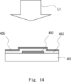
- FIG. 13 and 14 are process cross-sectional views showing the manufacturing process of the semiconductor device.
- a method of manufacturing a semiconductor device having an inverted staggered type TFT will be described.
- 13 and 14 show the process of forming a polysilicon film in the semiconductor manufacturing method. For other manufacturing steps, a known method can be used, so the description is omitted.
- a gate electrode 402 is formed on a glass substrate 401 .
- a gate insulating film 403 is formed on the gate electrode 402 .
- An amorphous silicon film 404 is formed on the gate insulating film 403 .
- the amorphous silicon film 404 is arranged so as to overlap the gate electrode 402 with the gate insulating film 403 interposed therebetween.
- the gate insulating film 403 and the amorphous silicon film 404 are continuously formed by CVD (Chemical Vapor Deposition).
- a polysilicon film 405 is formed as shown in FIG. That is, the amorphous silicon film 404 is dehydrogenated by the laser irradiation apparatus 1 described above. Further, the amorphous silicon film 404 is crystallized by the laser irradiation apparatus 1 of the second and third embodiments. As a result, a polysilicon film 405 of crystallized silicon is formed on the gate insulating film 403 .
- the amorphous silicon film 404 or polysilicon film 405 corresponds to the film 16b described above.
- the laser annealing apparatus irradiates the amorphous silicon film with the laser beam to form the polysilicon film. It may form a microcrystalline silicon film.
- laser light for annealing is not limited to blue laser diodes and Nd:YAG lasers.
- the method according to the present embodiment can also be applied to a laser irradiation apparatus that irradiates a thin film other than a silicon film with a laser beam. That is, the method according to the present embodiment can be applied to any laser irradiation apparatus that forms a crystallized film by irradiating an amorphous film with a laser beam.
- the laser irradiation apparatus 1 can also be applied to laser annealing treatment 2 for dehydrogenating thin films other than silicon films.
- the crystallized film-coated substrate can be appropriately modified.
- the laser irradiation method according to this embodiment is a laser irradiation method for dehydrogenating a film provided on a substrate.
- a laser irradiation method comprises the steps of: generating a blue laser beam with a semiconductor laser light source; guiding the laser beam to a substrate with an optical system unit; and changing the irradiation position of the laser beam with respect to the substrate. I have it.
- Embodiments 1 to 3 can be used in combination as appropriate. It should be noted that the present invention is not limited to the above embodiments, and can be modified as appropriate without departing from the scope of the invention.
Abstract
Dispositif d'irradiation laser (1) selon un mode de réalisation de la présente invention comprend : une source de lumière laser (35) ; une unité de système optique (30) qui guide un faisceau laser (15) vers un substrat ; une unité flottante (10) qui a un trou débouchant disposé directement au-dessous de la position d'irradiation avec le faisceau laser (15) et amène le substrat à flotter ; une unité de transport (11) qui transporte le substrat flottant sur l'unité flottante (10) dans une première direction ; et une étape (40) qui est disposée sur l'unité flottante (10) et qui maintient l'unité de système optique (30) de façon à être mobile dans une seconde direction différente de la première direction dans une vue de dessus.
Priority Applications (1)
| Application Number | Priority Date | Filing Date | Title |
|---|---|---|---|
| PCT/JP2021/040657 WO2023079648A1 (fr) | 2021-11-04 | 2021-11-04 | Dispositif d'irradiation laser, procédé d'irradiation laser et procédé de fabrication d'un dispositif d'affichage |
Applications Claiming Priority (1)
| Application Number | Priority Date | Filing Date | Title |
|---|---|---|---|
| PCT/JP2021/040657 WO2023079648A1 (fr) | 2021-11-04 | 2021-11-04 | Dispositif d'irradiation laser, procédé d'irradiation laser et procédé de fabrication d'un dispositif d'affichage |
Publications (1)
| Publication Number | Publication Date |
|---|---|
| WO2023079648A1 true WO2023079648A1 (fr) | 2023-05-11 |
Family
ID=86240821
Family Applications (1)
| Application Number | Title | Priority Date | Filing Date |
|---|---|---|---|
| PCT/JP2021/040657 WO2023079648A1 (fr) | 2021-11-04 | 2021-11-04 | Dispositif d'irradiation laser, procédé d'irradiation laser et procédé de fabrication d'un dispositif d'affichage |
Country Status (1)
| Country | Link |
|---|---|
| WO (1) | WO2023079648A1 (fr) |
Citations (9)
| Publication number | Priority date | Publication date | Assignee | Title |
|---|---|---|---|---|
| JPH08129189A (ja) * | 1992-11-16 | 1996-05-21 | Tokyo Electron Ltd | 液晶ディスプレイ基板の製造方法、その装置、半導体結晶の評価方法、半導体結晶薄膜の製造方法及び半導体結晶薄膜の製造装置 |
| JPH10242073A (ja) * | 1997-02-28 | 1998-09-11 | Semiconductor Energy Lab Co Ltd | レーザー照射装置およびレーザー照射方法 |
| JPH11251261A (ja) * | 1998-03-04 | 1999-09-17 | Seiko Epson Corp | 半導体膜の製造方法、およびアニール装置及び薄膜トランジスタの製造方法及び液晶表示装置用アクティブマトリクス基板 |
| JP2002158173A (ja) * | 2000-09-05 | 2002-05-31 | Sony Corp | 薄膜の製造方法、半導体薄膜、半導体装置、半導体薄膜の製造方法、及び半導体薄膜製造装置 |
| JP2009135430A (ja) * | 2007-10-10 | 2009-06-18 | Semiconductor Energy Lab Co Ltd | 半導体装置の作製方法 |
| JP2010141190A (ja) * | 2008-12-12 | 2010-06-24 | Shimadzu Corp | レーザ結晶化装置 |
| JP2017152498A (ja) * | 2016-02-23 | 2017-08-31 | 株式会社ブイ・テクノロジー | レーザアニール方法、レーザアニール装置及び薄膜トランジスタ基板 |
| JP2018060888A (ja) * | 2016-10-04 | 2018-04-12 | 株式会社日本製鋼所 | レーザ照射装置、半導体装置の製造方法、及び、レーザ照射装置の動作方法 |
| JP2020145362A (ja) * | 2019-03-08 | 2020-09-10 | 株式会社日本製鋼所 | レーザ処理装置 |
-
2021
- 2021-11-04 WO PCT/JP2021/040657 patent/WO2023079648A1/fr active Application Filing
Patent Citations (9)
| Publication number | Priority date | Publication date | Assignee | Title |
|---|---|---|---|---|
| JPH08129189A (ja) * | 1992-11-16 | 1996-05-21 | Tokyo Electron Ltd | 液晶ディスプレイ基板の製造方法、その装置、半導体結晶の評価方法、半導体結晶薄膜の製造方法及び半導体結晶薄膜の製造装置 |
| JPH10242073A (ja) * | 1997-02-28 | 1998-09-11 | Semiconductor Energy Lab Co Ltd | レーザー照射装置およびレーザー照射方法 |
| JPH11251261A (ja) * | 1998-03-04 | 1999-09-17 | Seiko Epson Corp | 半導体膜の製造方法、およびアニール装置及び薄膜トランジスタの製造方法及び液晶表示装置用アクティブマトリクス基板 |
| JP2002158173A (ja) * | 2000-09-05 | 2002-05-31 | Sony Corp | 薄膜の製造方法、半導体薄膜、半導体装置、半導体薄膜の製造方法、及び半導体薄膜製造装置 |
| JP2009135430A (ja) * | 2007-10-10 | 2009-06-18 | Semiconductor Energy Lab Co Ltd | 半導体装置の作製方法 |
| JP2010141190A (ja) * | 2008-12-12 | 2010-06-24 | Shimadzu Corp | レーザ結晶化装置 |
| JP2017152498A (ja) * | 2016-02-23 | 2017-08-31 | 株式会社ブイ・テクノロジー | レーザアニール方法、レーザアニール装置及び薄膜トランジスタ基板 |
| JP2018060888A (ja) * | 2016-10-04 | 2018-04-12 | 株式会社日本製鋼所 | レーザ照射装置、半導体装置の製造方法、及び、レーザ照射装置の動作方法 |
| JP2020145362A (ja) * | 2019-03-08 | 2020-09-10 | 株式会社日本製鋼所 | レーザ処理装置 |
Similar Documents
| Publication | Publication Date | Title |
|---|---|---|
| JP6983578B2 (ja) | レーザ照射装置、レーザ照射方法、及び半導体装置の製造方法 | |
| US20210066082A1 (en) | Laser irradiation apparatus and method for manufacturing semiconductor device | |
| US7476629B2 (en) | Beam irradiation apparatus, beam irradiation method, and method for manufacturing thin film transistor | |
| WO2010001727A1 (fr) | Dispositif de recuit laser | |
| JP2003059858A (ja) | レーザアニール装置及び薄膜トランジスタの製造方法 | |
| JP6764305B2 (ja) | レーザ照射装置、半導体装置の製造方法、及び、レーザ照射装置の動作方法 | |
| CN112136361A (zh) | 柔性发光器件的制造方法以及制造装置 | |
| JP2002217125A (ja) | 表面処理装置及び方法 | |
| JP5037926B2 (ja) | レーザアニール装置 | |
| JP2005081715A (ja) | レーザ加工装置およびレーザ加工方法 | |
| TW201328811A (zh) | 分斷裝置、被加工物之分斷方法、及具有光學元件圖案之基板的分斷方法 | |
| WO2023079648A1 (fr) | Dispositif d'irradiation laser, procédé d'irradiation laser et procédé de fabrication d'un dispositif d'affichage | |
| US20100291760A1 (en) | Method and system for spatially selective crystallization of amorphous silicon | |
| US9755190B2 (en) | Laser-induced thermal imaging apparatus, method of laser-induced thermal imaging, and manufacturing method of organic light-emitting display apparatus using the method | |
| WO2018097087A1 (fr) | Dispositif de recuit laser | |
| JP2004006703A (ja) | 半導体のアニールおよびドーピングのための処理方法ならびにその装置 | |
| WO2023095188A1 (fr) | Dispositif d'irradiation laser, procédé d'irradiation laser et procédé de fabrication de dispositif semi-conducteur | |
| JP4363010B2 (ja) | レーザアニール装置 | |
| JP2008244195A (ja) | レーザアニール装置 | |
| JP4215563B2 (ja) | 半導体薄膜改質方法 | |
| US20200251359A1 (en) | Laser radiation system | |
| KR102426156B1 (ko) | 이중 파장 어닐링 방법 및 장치 | |
| WO2019234856A1 (fr) | Procédé de recuit au laser, appareil de recuit au laser et procédé de production de substrat matriciel actif | |
| WO2021038950A1 (fr) | Dispositif et procédé de traitement laser pour la fabrication d'un dispositif à semi-conducteur | |
| CN213366530U (zh) | 激光退火装置 |
Legal Events
| Date | Code | Title | Description |
|---|---|---|---|
| 121 | Ep: the epo has been informed by wipo that ep was designated in this application |
Ref document number: 21963244 Country of ref document: EP Kind code of ref document: A1 |
|
| WWE | Wipo information: entry into national phase |
Ref document number: 2023557510 Country of ref document: JP |