WO2023079648A1 - Laser irradiation device, laser irradiation method, and method for manufacturing display - Google Patents
Laser irradiation device, laser irradiation method, and method for manufacturing display Download PDFInfo
- Publication number
- WO2023079648A1 WO2023079648A1 PCT/JP2021/040657 JP2021040657W WO2023079648A1 WO 2023079648 A1 WO2023079648 A1 WO 2023079648A1 JP 2021040657 W JP2021040657 W JP 2021040657W WO 2023079648 A1 WO2023079648 A1 WO 2023079648A1
- Authority
- WO
- WIPO (PCT)
- Prior art keywords
- laser light
- substrate
- laser
- irradiation
- optical system
- Prior art date
Links
- 238000000034 method Methods 0.000 title claims description 62
- 238000004519 manufacturing process Methods 0.000 title claims description 34
- 239000000758 substrate Substances 0.000 claims abstract description 146
- 230000003287 optical effect Effects 0.000 claims abstract description 107
- 238000007667 floating Methods 0.000 claims abstract description 29
- 230000007246 mechanism Effects 0.000 claims description 53
- 230000032258 transport Effects 0.000 claims description 51
- 239000004065 semiconductor Substances 0.000 claims description 44
- 238000005339 levitation Methods 0.000 claims description 32
- 238000002425 crystallisation Methods 0.000 claims description 26
- 230000008025 crystallization Effects 0.000 claims description 26
- 230000001678 irradiating effect Effects 0.000 claims description 25
- 238000007493 shaping process Methods 0.000 claims description 15
- 230000008859 change Effects 0.000 claims description 11
- 239000010408 film Substances 0.000 description 140
- 229910021417 amorphous silicon Inorganic materials 0.000 description 24
- 230000008569 process Effects 0.000 description 21
- XUIMIQQOPSSXEZ-UHFFFAOYSA-N Silicon Chemical compound [Si] XUIMIQQOPSSXEZ-UHFFFAOYSA-N 0.000 description 20
- 229910052710 silicon Inorganic materials 0.000 description 20
- 239000010703 silicon Substances 0.000 description 20
- 238000000137 annealing Methods 0.000 description 19
- 230000035515 penetration Effects 0.000 description 16
- 239000010410 layer Substances 0.000 description 14
- 238000006356 dehydrogenation reaction Methods 0.000 description 13
- 229910021420 polycrystalline silicon Inorganic materials 0.000 description 12
- 229920005591 polysilicon Polymers 0.000 description 12
- UFHFLCQGNIYNRP-UHFFFAOYSA-N Hydrogen Chemical compound [H][H] UFHFLCQGNIYNRP-UHFFFAOYSA-N 0.000 description 8
- 239000001257 hydrogen Substances 0.000 description 8
- 229910052739 hydrogen Inorganic materials 0.000 description 8
- 239000000463 material Substances 0.000 description 7
- 239000012044 organic layer Substances 0.000 description 7
- 239000007789 gas Substances 0.000 description 6
- 239000011521 glass Substances 0.000 description 5
- 230000004048 modification Effects 0.000 description 5
- 238000012986 modification Methods 0.000 description 5
- 239000013307 optical fiber Substances 0.000 description 5
- 238000005224 laser annealing Methods 0.000 description 4
- 238000007789 sealing Methods 0.000 description 4
- 239000010409 thin film Substances 0.000 description 4
- 238000010521 absorption reaction Methods 0.000 description 3
- 238000001816 cooling Methods 0.000 description 3
- 238000006073 displacement reaction Methods 0.000 description 3
- 238000010438 heat treatment Methods 0.000 description 3
- 239000011148 porous material Substances 0.000 description 3
- 239000011347 resin Substances 0.000 description 3
- 229920005989 resin Polymers 0.000 description 3
- 238000001004 secondary ion mass spectrometry Methods 0.000 description 3
- 239000004696 Poly ether ether ketone Substances 0.000 description 2
- 230000008033 biological extinction Effects 0.000 description 2
- 238000005229 chemical vapour deposition Methods 0.000 description 2
- 239000011159 matrix material Substances 0.000 description 2
- 239000012528 membrane Substances 0.000 description 2
- 229910052751 metal Inorganic materials 0.000 description 2
- 239000002184 metal Substances 0.000 description 2
- 239000007769 metal material Substances 0.000 description 2
- 229920002530 polyetherether ketone Polymers 0.000 description 2
- 230000003746 surface roughness Effects 0.000 description 2
- 229910000838 Al alloy Inorganic materials 0.000 description 1
- RYGMFSIKBFXOCR-UHFFFAOYSA-N Copper Chemical compound [Cu] RYGMFSIKBFXOCR-UHFFFAOYSA-N 0.000 description 1
- VYPSYNLAJGMNEJ-UHFFFAOYSA-N Silicium dioxide Chemical compound O=[Si]=O VYPSYNLAJGMNEJ-UHFFFAOYSA-N 0.000 description 1
- 229910052782 aluminium Inorganic materials 0.000 description 1
- XAGFODPZIPBFFR-UHFFFAOYSA-N aluminium Chemical compound [Al] XAGFODPZIPBFFR-UHFFFAOYSA-N 0.000 description 1
- PNEYBMLMFCGWSK-UHFFFAOYSA-N aluminium oxide Inorganic materials [O-2].[O-2].[O-2].[Al+3].[Al+3] PNEYBMLMFCGWSK-UHFFFAOYSA-N 0.000 description 1
- 229910010293 ceramic material Inorganic materials 0.000 description 1
- 229910052802 copper Inorganic materials 0.000 description 1
- 239000010949 copper Substances 0.000 description 1
- 229910021419 crystalline silicon Inorganic materials 0.000 description 1
- 230000007423 decrease Effects 0.000 description 1
- 230000001419 dependent effect Effects 0.000 description 1
- 230000006866 deterioration Effects 0.000 description 1
- 238000010586 diagram Methods 0.000 description 1
- 238000009792 diffusion process Methods 0.000 description 1
- 230000000694 effects Effects 0.000 description 1
- 238000005401 electroluminescence Methods 0.000 description 1
- 230000017525 heat dissipation Effects 0.000 description 1
- 238000005286 illumination Methods 0.000 description 1
- 238000005499 laser crystallization Methods 0.000 description 1
- 229910021424 microcrystalline silicon Inorganic materials 0.000 description 1
- 229910021421 monocrystalline silicon Inorganic materials 0.000 description 1
- 238000005192 partition Methods 0.000 description 1
- 230000009467 reduction Effects 0.000 description 1
- 229910052814 silicon oxide Inorganic materials 0.000 description 1
- 238000009751 slip forming Methods 0.000 description 1
- 238000001179 sorption measurement Methods 0.000 description 1
- XLYOFNOQVPJJNP-UHFFFAOYSA-N water Substances O XLYOFNOQVPJJNP-UHFFFAOYSA-N 0.000 description 1
Images


Classifications
-
- H—ELECTRICITY
- H01—ELECTRIC ELEMENTS
- H01L—SEMICONDUCTOR DEVICES NOT COVERED BY CLASS H10
- H01L21/00—Processes or apparatus adapted for the manufacture or treatment of semiconductor or solid state devices or of parts thereof
- H01L21/02—Manufacture or treatment of semiconductor devices or of parts thereof
- H01L21/04—Manufacture or treatment of semiconductor devices or of parts thereof the devices having at least one potential-jump barrier or surface barrier, e.g. PN junction, depletion layer or carrier concentration layer
- H01L21/18—Manufacture or treatment of semiconductor devices or of parts thereof the devices having at least one potential-jump barrier or surface barrier, e.g. PN junction, depletion layer or carrier concentration layer the devices having semiconductor bodies comprising elements of Group IV of the Periodic System or AIIIBV compounds with or without impurities, e.g. doping materials
- H01L21/26—Bombardment with radiation
- H01L21/263—Bombardment with radiation with high-energy radiation
- H01L21/268—Bombardment with radiation with high-energy radiation using electromagnetic radiation, e.g. laser radiation
Definitions
- the present invention relates to a laser irradiation device, a laser irradiation method, and a display manufacturing method.
- Patent Document 1 discloses a laser annealing apparatus using an excimer laser.
- the transport unit transports the substrate while the floating unit floats the substrate. Then, the substrate being transported is irradiated with the line-shaped laser beam.
- the laser irradiation device is a laser irradiation device that irradiates a film provided on a substrate with a laser beam, and is a laser light source that generates a laser beam having a wavelength at least part of which is transmitted through the film. and an optical system unit that guides the laser beam to the substrate, and a levitation unit that has a through hole provided immediately below the irradiation position of the laser beam and floats the substrate.
- a laser irradiation apparatus includes a semiconductor laser light source that generates a laser beam having a wavelength of 500 nm or less, a transport unit that transports a substrate in a first direction, and a pulsed laser beam that emits the laser beam to the substrate. and a driving mechanism for driving the optical system unit so as to change the irradiation position of the laser beam with respect to the substrate in a second direction different from the first direction when viewed from above.
- the laser irradiation device is a laser irradiation device that dehydrogenates a film provided on a substrate, and includes a semiconductor laser light source that generates a laser beam having a wavelength of 500 nm or less; An optical system unit that guides a laser beam to a substrate and a drive mechanism that changes the irradiation position of the laser beam on the substrate are provided.
- a laser irradiation apparatus includes a transport unit that generates a substrate on which a film is formed in a first direction, a semiconductor laser light source that generates a laser beam with a wavelength of 500 nm or less, and a substrate that emits the laser beam. a driving mechanism for changing the irradiation position of the laser beam with respect to the substrate in a second direction inclined from the first direction when viewed from above; and an excimer laser for crystallizing the film.
- an excimer laser light source that generates light; and an optical system for crystallization that guides the excimer laser light to the substrate being transported as a linear line beam having a longitudinal direction inclined from the first direction when viewed from above. and have.
- the laser irradiation method is a laser irradiation method for irradiating a film provided on a substrate with a laser beam, comprising: (A1) a through hole provided immediately below the laser beam irradiation position; (A2) generating a laser beam having a wavelength at least a portion of which is transmitted through the film; leading to the substrate.
- the laser irradiation method includes the steps of (B1) generating laser light with a wavelength of 500 nm or less using a semiconductor laser light source, and (B2) transporting the substrate in a first direction by a transport unit. (B3) guiding the laser light, which is a pulsed light, to the substrate by an optical system unit; and (B4) irradiating the substrate with the laser light in a second direction different from the first direction when viewed from above. and C. driving the optics unit to change position.
- the laser irradiation method is a laser irradiation method for performing a dehydrogenation treatment on a film provided on a substrate, and (C1) emits a laser beam having a wavelength of 500 nm or less from a semiconductor laser light source. (C2) guiding the laser light to the substrate by an optical system unit; and (C3) changing the irradiation position of the laser light on the substrate.
- the laser irradiation method comprises the steps of: (D1) transporting a substrate having a film formed thereon in a first direction by a transport unit; (D3) guiding the laser beam to the substrate by an optical system unit; (D5) generating an excimer laser beam for crystallizing the film from an excimer laser light source; (D6) directing the excimer laser beam in the first direction when viewed from above; and guiding the light beam to the substrate being transported as a line-shaped line beam whose longitudinal direction is the direction inclined from the vertical direction.
- the display manufacturing method includes (S1) an irradiation step of irradiating a film formed on a substrate with a laser beam, and the (S1) irradiation step includes (SA1) the irradiation of the laser beam.
- SA2 generating a laser beam having a wavelength at least partially transmitted through the film;
- SA3 optical and guiding the laser light to the floating substrate by a system unit.
- the display manufacturing method includes (S1) an irradiation step of irradiating a film formed on a substrate with laser light, and the (S1) irradiation step includes (SB1) a semiconductor laser light source.
- (SB2) transporting a substrate in a first direction by a transport unit; and (SB3) guiding the laser beam, which is pulsed light, to the substrate by an optical system unit.
- (SB4) driving the optical system unit so as to change the irradiation position of the laser light on the substrate in a second direction different from the first direction when viewed from above.
- the display manufacturing method includes (T1) an irradiation step of irradiating the film formed on the substrate with a laser beam in order to dehydrogenate the film, and the ( T1)
- the irradiating step includes (TC1) generating laser light with a wavelength of 500 nm or less from a semiconductor laser light source, (TC2) guiding the laser light to a substrate by an optical system unit, and (TC3) and changing the irradiation position of the laser light.
- the display manufacturing method includes (S1) an irradiation step of irradiating a film formed on a substrate with a laser beam, and the (S1) irradiation step includes (SD1) a transport unit, (SD2) generating a laser beam with a wavelength of 500 nm or less using a semiconductor laser light source; (SD4) changing the irradiation position of the laser beam with respect to the substrate in a second direction different from the first direction when viewed from the top; (SD5) exposing the film to the (SD6) generating an excimer laser beam for crystallization; and (SD6) the excimer laser beam being transported as a line-shaped line beam having a longitudinal direction inclined from the first direction when viewed from above. leading to the substrate.
- SD1 a transport unit
- SD2 generating a laser beam with a wavelength of 500 nm or less using a semiconductor laser light source
- SD4 changing the irradiation position of the laser beam with respect to the substrate in a second direction different from the first direction when
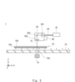
- FIG. 1 is a top view schematically showing a laser irradiation device according to an embodiment
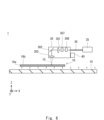
- FIG. 1 is an XZ sectional view schematically showing a laser irradiation device according to an embodiment
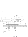
- FIG. 1 is a YZ sectional view schematically showing a laser irradiation device according to an embodiment
- FIG. 4 is a table showing the penetration depth of silicon membranes
- It is an XZ sectional view which shows typically the laser irradiation apparatus concerning a modification.
- FIG. 3 is a side view schematically showing a laser irradiation device according to a second embodiment
- FIG. It is a top view which shows the spot shape of a laser beam typically.
- FIG. 1 is a top view schematically showing a laser irradiation device according to an embodiment
- FIG. 1 is an XZ sectional view schematically showing a laser irradiation device according to an embodiment
- FIG. 1 is a YZ sectional view schematically showing a laser i
- FIG. 11 is a top view schematically showing a laser irradiation device according to a third embodiment;
- FIG. 11 is a side view schematically showing a laser irradiation device according to a third embodiment;
- 4 is a photograph showing an annealed silicon film;
- FIG. 4 is a SIMS profile showing hydrogen concentration in an annealed silicon film;
- FIG. 1 is a cross-sectional view showing a simplified configuration of an organic EL display;
- FIG. It is process sectional drawing which shows the manufacturing method of the display concerning this Embodiment. It is process sectional drawing which shows the manufacturing method of the display concerning this Embodiment.
- the laser irradiation apparatus performs annealing by irradiating an object to be processed (also referred to as a work) with a laser beam.
- the laser irradiation apparatus heats the substrate with laser light to perform dehydrogenation annealing treatment on a film provided on the substrate.
- the object to be processed is a film-coated substrate on which a silicon film is formed.
- the laser irradiation device uses a blue semiconductor laser light source as a laser light source.
- the laser irradiation device irradiates the object to be processed with a blue laser beam from a semiconductor laser light source, thereby performing a dehydrogenation process on the silicon film.
- Laser light is not limited to blue laser light, and laser light with a wavelength of 500 nm or less can be used.
- a film forming device forms a film on a substrate. Then, a laser irradiation device irradiates the film with a laser beam.
- the substrate is, for example, a transparent substrate such as a glass substrate or a resin substrate, and the film is, for example, an amorphous silicon film.
- a substrate with an amorphous silicon film is an object to be processed.
- the laser irradiation device dehydrogenates the amorphous silicon film by irradiating the amorphous silicon film with laser light.
- the object to be processed may be a film-coated substrate on which a film other than a silicon film is formed.
- the laser irradiation apparatus is a dehydrogenation annealing apparatus using laser light, but it may be a crystallization annealing apparatus for crystallizing an amorphous silicon film by laser irradiation.
- FIG. 1 is a top view schematically showing the configuration of a laser irradiation device 1.
- FIG. 2 is an XZ sectional view schematically showing the configuration of the laser irradiation device 1.
- FIG. 3 is a YZ cross-sectional view schematically showing the configuration of the laser irradiation device 1. As shown in FIG.
- the laser irradiation device 1 includes a levitation unit 10, a transport unit 11, an optical system unit 30, a Y driving mechanism 32, and a stage 40.
- the levitation unit 10 and the transport unit 11 constitute a transport device.
- the diagrams shown below show an XYZ three-dimensional orthogonal coordinate system as appropriate for simplification of explanation.
- the Z direction is a vertical up-down direction, and is a direction perpendicular to the main surface of the object 16 to be processed.
- the X direction is the transport direction of the object 16 to be processed.
- the Y direction is the moving direction of the optical system unit 30 .
- a laser beam 15 is applied to an object 16 being transported in the X direction.
- the optical system unit 30 moves in the Y direction. Therefore, the irradiation position of the laser beam on the object to be processed 16 can be changed in the X direction and the Y direction. As a result, substantially the entire surface of the object 16 to be processed can be irradiated with the laser beam.
- the levitation unit 10 is configured to eject gas from the surface of the levitation unit 10 .
- the levitation unit 10 levitates the object 16 to be processed on its upper surface.
- the gas ejected from the surface of the floating unit 10 is sprayed onto the lower surface of the object 16 to float, thereby causing the object 16 to float.
- the floating unit 10 adjusts the floating amount so that the object 16 to be processed does not come into contact with another mechanism (not shown) arranged above the object 16 to be processed.
- the floating unit 10 is made of a porous material.
- the floating unit 10 is made of a ceramic material such as porous alumina or porous SiC.
- the levitation unit 10 is a porous material plate with a thickness of 10 mm.
- the floating unit 10 is connected to an air supply port (not shown). Therefore, gas from a gas supply means (not shown) such as a gas cylinder is jetted out from the upper surface of the levitation unit 10 .
- the transport unit 11 transports the floating object to be processed 16 in the transport direction.
- the transport unit 11 has a holding mechanism 12 and a moving mechanism 13 .
- the holding mechanism 12 holds the object 16 to be processed.
- the holding mechanism 12 can be configured using a vacuum suction mechanism.
- the vacuum adsorption mechanism is made of metal material such as aluminum alloy.
- the holding mechanism 12 may be made of a resin-based material such as PEEK (polyetheretherketone) material.
- a suction groove, a suction hole, and the like are formed on the upper surface of the holding mechanism 12 .
- the holding mechanism 12 may be made of a porous material.
- the holding mechanism 12 vacuum suction mechanism
- the holding mechanism 12 is connected to an exhaust port (not shown), and the exhaust port is connected to an ejector, a vacuum pump, and the like. Therefore, since a negative pressure for sucking gas acts on the holding mechanism 12 , the object to be processed 16 can be held using the holding mechanism 12 .
- the holding mechanism 12 sucks the surface (lower surface) of the object 16 to be processed that is opposite to the surface (upper surface) irradiated with the laser beam 15 , that is, the surface of the object 16 to be processed that faces the levitation unit 10 . and holds the object 16 to be processed. In addition, the holding mechanism 12 holds the +Y-direction end of the object 16 to be processed.
- a moving mechanism 13 provided in the transport unit 11 is connected to the holding mechanism 12 .
- the moving mechanism 13 is configured to move the holding mechanism 12 in the transport direction.
- the transport unit 11 (holding mechanism 12 and moving mechanism 13) is provided on the +Y-direction end side of the levitation unit 10. While the holding mechanism 12 holds the object to be processed 16, the moving mechanism 13 moves in the transport direction.
- the object to be processed 16 is conveyed by moving.
- the moving mechanism 13 is configured to slide the end of the levitation unit 10 in the +Y direction along the transport direction.
- the moving mechanism 13 slides the end of the levitation unit 10 along the transport direction, thereby transporting the workpiece 16 along the transport direction.
- the moving mechanism 13 includes, for example, an actuator such as a motor (not shown), a linear guide mechanism, an air bearing, and the like.
- the object 16 to be processed is a rectangular substrate having edges parallel to the X direction and the Y direction.
- the object 16 to be processed includes a substrate 16a and a film 16b formed on the substrate 16a.
- the substrate 16a is a transparent substrate such as a glass substrate.
- Film 16b is a silicon film, such as an amorphous silicon film. By irradiating the film 16b with the laser light 15 for annealing, hydrogen contained in the film 16b can be removed. That is, the laser irradiation device 1 serves as a dehydrogenation device.
- the film 16b which is a silicon film, is shown, other films may be formed.
- a thin film of copper or aluminum that serves as wiring may be formed as a base film of the silicon film.
- an insulating film such as a silicon oxide film may be formed on the substrate 16a as a base film.
- a stage 40 is arranged above the levitation unit 10 .
- the stage 40 movably holds the optical system unit 30 .
- the optical system unit 30 guides the laser light from the laser light source 35 to the object 16 to be processed.
- the optical system unit 30 is arranged on the ⁇ X side of the stage 40 . Therefore, the optical system unit 30 is arranged directly above the object 16 to be processed. Therefore, the object to be processed 16 is irradiated with the laser beam 15 from the optical system unit 30 from above.
- the stage 40 serves as a guide mechanism that guides the movement of the optical system unit 30 in the Y direction.
- the stage 40 is provided with guide rails, guide grooves, and the like.
- a Y drive mechanism 32 is also provided on the stage 40 .
- the stage 40 is a gantry stage provided along the Y direction in the space above the levitation unit 10 .
- a Y drive mechanism 32 drives the optical system unit 30 in the Y direction.
- the optical system unit 30 moves along the stage 40. Since the optical system unit 30 moves in the Y direction, the irradiation position of the laser beam 15 changes in the Y direction.
- the stage 40 is arranged to protrude from the levitation unit 10 on the +Y side and the -Y side. Therefore, in the Y direction, the optical system unit 30 can irradiate laser light to any position on the object 16 to be processed.
- the laser light source 35 generates laser light for annealing the object 16 to be processed.
- the laser light source 35 is a BLD (Blue Laser Diode) that generates blue laser light with a central wavelength of 450 nm. That is, the laser light source 35 is a blue semiconductor laser light source.
- the laser light is a continuous wave (CW) laser light.
- the laser irradiation device 1 may use a modulator or the like to modulate the laser light into a pulsed laser light.
- a laser light source 35 is coupled to an optical fiber 36 .
- Laser light from the laser light source 35 enters the optical system unit 30 via the optical fiber 36 .
- the optical system unit 30 has a lens 301, a mirror 302, and a lens 303.
- the optical system unit 30 may be provided with optical elements other than the lens 301 , the mirror 302 and the lens 303 .
- the spot shape of the laser beam 15 is a line shape of 10 mm ⁇ 0.3 mm.
- the laser light 15 is CW light, and the irradiation time at one point on the object 16 to be processed is set to 10 ⁇ sec to 1 sec.
- a laser beam from the optical fiber 36 enters the lens 301 .
- a laser beam condensed by the lens 301 is incident on the mirror 302 .
- the mirror 302 reflects the laser light toward the object 16 to be processed. Specifically, the mirror 302 reflects the laser light downward.
- the laser beam reflected by the mirror 302 enters the lens 303 .
- the object 16 to be processed is irradiated with the laser beam 15 from the lens 303 .
- the lens 303 converges the laser beam 15 onto the object 16 to be processed. Therefore, the laser beam 15 from the optical system unit 30 becomes a converging beam and is irradiated onto the object 16 to be processed.
- the optical system unit 30 irradiates the object 16 to be processed with the laser beam 15 from above.
- the film 16b of the object 16 to be processed is annealed, and dehydrogenation treatment can be performed on the film 16b.
- the optical axis of the lens 303 is parallel to the Z direction, it may be tilted from the Z direction.
- the laser light source 35 is a blue semiconductor laser light source
- the laser light 15 is blue laser light.
- the center wavelength of the laser light 15 is 450 nm. Blue light has a deep penetration depth into the silicon film. Therefore, not all of the laser beam 15 is absorbed by the object 16 to be processed, and part of the laser beam 15 is transmitted through the object 16 to be processed.
- the levitation unit 10 is heated. Therefore, the temperature of the levitation unit 10 fluctuates during the process. Furthermore, since the laser light is reflected or scattered on the surface of the levitation unit 10 , the laser light from directly below the irradiated portion enters the object 16 to be processed again. Therefore, the annealing process for dehydrogenation may become unstable.
- the levitation unit 10 is provided with a through hole 10a directly below the irradiation location of the laser beam 15.
- FIG. When viewed from above, the through hole 10a is formed in a belt-like region having the Y direction as the longitudinal direction.
- the laser beam 15 does not enter the levitation unit 10 because it passes through the through hole 10a. Absorption, reflection or scattering of the laser light 15 in the levitation unit 10 can be prevented.
- the width of the through hole 10a in the X direction is about 10 mm.
- the length of the through hole 10 a in the Y direction is approximately the same as the movable range of the optical system unit 30 .
- the temperature of the levitation unit 10 can be stabilized. Furthermore, it is possible to prevent reflected light or scattered light from the floating unit 10 from entering the object 16 again. Reflected light and scattered light from the surface of the levitation unit 10 can be reduced. By doing so, a stable dehydrogenation process becomes possible, and productivity can be improved.
- the Y drive mechanism 32 drives the optical system unit 30 while the transport unit 11 transports the object 16 to be processed. That is, the Y drive mechanism 32 moves the irradiation position of the laser beam in the Y direction, and the transport unit 11 moves the object 16 to be processed in the X direction. Therefore, the irradiation position of the laser beam on the object to be processed 16 changes in the X direction and the Y direction. As a result, substantially the entire surface of the object 16 to be processed can be irradiated with the laser beam. Therefore, almost the entire film 16b can be annealed, and the dehydrogenation treatment can be appropriately performed.
- the moving speed of the optical system unit 30 in the Y direction may be faster than the transport speed in the X direction.
- the laser irradiation position can be changed at high speed in the Y direction. Therefore, since local heating can be prevented, an influence on a base film or the like can be prevented.
- the laser light source 35 is not limited to this. Specifically, when a film 16b having a predetermined thickness is provided on the substrate 16a, the laser light source 35 may generate laser light having a wavelength that at least part of the laser light passes through the film 16b. Just do it.
- the penetration depth (penetration depth) for light with a wavelength of 450 nm is 0.02 ⁇ m.
- the penetration depth is the thickness of a material when the amount of light incident on the material becomes 1/e. e is the Napier number.
- the penetration depth is determined by the material's extinction coefficient. Also, the extinction coefficient is wavelength dependent. The depth of penetration is determined by the material of the membrane and the wavelength of the light.
- FIG. 4 is a table showing penetration depths of an amorphous silicon (a-Si) film and a single crystal silicon (c-Si) film.
- FIG. 4 shows the penetration depth for light with wavelengths of 308 nm, 355 nm, 450 nm, 532 nm and 808 nm.
- the penetration depth is the film thickness when the absorptance becomes 1/e (63%). If the film 16b is an amorphous silicon film and the laser wavelength is 450 nm, the penetration depth is 0.02 ⁇ m.
- the laser irradiation apparatus 1 is suitable for annealing the film 16b having a film thickness of four times or less the penetration depth. In other words, when annealing a film having a film thickness greater than four times the penetration depth, the effect on the levitation unit 10 is minor. If the thickness of the film 16b is determined, the range of laser wavelength suitable for this embodiment is determined.
- the film 16b is an amorphous silicon film with a thickness of 40 nm.
- the penetration depth is 10 nm when the laser wavelength is 355 nm.
- the laser wavelength is 355 nm or more
- 2% or more of the laser light is transmitted through the film 16b, which affects the process.
- 2% or more of the laser light passes through the film 16b.
- Absorption, reflection, or scattering at the levitation unit 10 can cause process variations.
- the laser irradiation apparatus is suitable when laser light with a wavelength of 355 nm or more and 808 nm or less is used. That is, it is suitable for annealing a film having a film thickness four times or less the penetration depth of light of a laser wavelength.
- the optical system unit 30 may have an optical scanner for scanning laser light.
- mirror 302 may be a galvanometric mirror.
- the optical scanner changes the irradiation position of the laser light by deflecting the laser light.
- the optical scanner is a uniaxial optical scanner that changes the irradiation position of the laser light in the X direction. That is, by changing the irradiation position of the optical scanner in the X direction, it is possible to shorten the irradiation time during which one point of the object 16 to be processed is continuously irradiated with the laser beam. This can prevent local heating of the base film or the like. Therefore, a stable annealing process becomes possible.
- lens 303 may be an f-theta lens. Thereby, even when the optical scanner deflects the laser light, the irradiation direction of the laser light can be made parallel to the Z direction.
- a laser irradiation method is a laser irradiation method for irradiating a film provided on a substrate with laser light.
- the laser irradiation method comprises the steps of: floating the substrate by a floating unit having a through hole provided immediately below a laser beam irradiation position; and transporting the substrate floating on the floating unit in a first direction. generating a laser beam having a wavelength at least part of which is transmitted through the film; guiding the laser beam to the substrate being transported by an optical system unit; and moving the optical system unit in a second direction so as to change the irradiation position of the laser light in a second direction different from the above.
- productivity can be improved.
- FIG. 5 is a side sectional view schematically showing the configuration of the laser irradiation device 1. As shown in FIG. In modification 1, a damper 19 is added to the configuration of the first embodiment.
- the damper 19 is arranged directly below the through hole 10a.
- the damper 19 absorbs the laser beam 15 that has passed through the through hole 10a.
- the damper 19 is a metal block whose longitudinal direction is the Y direction. The length can be approximately the same as that of the through hole 10a.
- the damper 19 is made of a metallic material or the like colored black.
- the damper 19 is arranged directly below the through-hole 10a in FIG. 5, the arrangement location of the damper 19 is not limited to directly below the through-hole 10a.
- a mirror or the like that reflects the blue laser light may be arranged directly below the through hole 10a.
- the damper 19 may be arranged at a position where it can absorb the laser beam reflected by the mirror. That is, the damper 19 absorbs the blue laser light reflected by the mirror.
- the damper 19 may be cooled.
- the damper 19 may be provided with a cooling mechanism such as an air cooling mechanism or a water cooling mechanism.
- the damper 19 may be provided with a heat dissipation mechanism. By doing so, the temperature rise of the damper 19 and its surroundings can be suppressed, so that the annealing process can be performed stably.
- FIG. 6 is a cross-sectional view schematically showing the configuration of the laser irradiation device 1.
- the laser irradiation device 1 is a laser crystallization device for crystallizing an amorphous silicon film.
- the film 16b before laser light irradiation is an amorphous silicon film.
- the film 16b after laser light irradiation is a polysilicon film.
- a laser light source 35 is a blue semiconductor laser light source. By irradiating the blue laser light, the film 16b becomes a polysilicon film.
- the laser irradiation device 1 has a modulator 306 and a beam shaping section 307 .
- the modulator 306 and beam shaping section 307 are mounted on the optical system unit 30 . Configurations other than the modulator 306 and the beam shaping section 307 are the same as those in the first embodiment, so description thereof will be omitted.
- a modulator 306 modulates the laser light. This modulates the CW laser light into pulsed laser light.
- the repetition frequency R of the pulsed laser light is 10 kHz to 200 kHz. It is preferable that the irradiation time during which the laser beam is continuously irradiated to one location of the object 16 to be processed is 1 ⁇ sec or less.
- the pulsed laser light from the modulator 306 enters the beam shaping section 307 .
- a beam shaping section 307 shapes the spot shape of the pulsed laser light.
- the beam shaping section 307 has a beam shaping mechanism such as a slit.
- the beam may be shaped by the placement of the output ends of the optical fibers 36 .
- the beam shaping section 307 shapes the beam so that the beam cross-sectional shape (spot shape) in the direction perpendicular to the optical axis is rectangular.
- the shape of the spot is rectangular with a size of 10 mm in the longitudinal direction and a size of 0.03 mm in the lateral direction.
- the spot shape of the beam on the object to be processed 16 will be described later.
- the pulsed laser light shaped by the beam shaping unit 307 is incident on the object to be processed 16 via the lens 301, the mirror 302 and the lens 303, as in the first embodiment.
- FIG. 7 shows the beam spot shape on the object 16 to be processed.
- FIG. 7 is an XY plan view schematically showing the spot shape of the pulsed laser beam on the object 16 to be processed.
- the transportation speed of the object to be processed 16 by the transportation unit 11 is sufficiently slower than the moving speed of the optical system unit 30 by the Y drive mechanism 32 .
- the sizes and the like shown below are examples of the present embodiment, and the present embodiment is not limited to the following sizes.
- the shape of the spot of the laser beam 15 on the object 16 to be processed is rectangular with a longitudinal direction.
- the size L of the spot shape in the longitudinal direction is 900 ⁇ m
- the size in the lateral direction is 15 ⁇ m.
- the lateral direction and the longitudinal direction are directions orthogonal to each other.
- the longitudinal direction is inclined from the X direction and the Y direction. Specifically, the angle ⁇ between the lateral direction and the Y direction is 45°. That is, the longitudinal direction of the spot shape is slanted by 45° from the moving direction of the optical system unit 30 .
- the moving speed V of the optical system unit 30 in the Y direction is 70.7 mm/s.
- the beam edge has a lower light intensity than the beam center. That is, the light intensity is highest at the center of the beam, and the light intensity decreases from the center of the beam toward the ends of the beam.
- the beam end portion with low light intensity is repeatedly irradiated many times, the surface roughness of the film 16b will differ from that of the other portions. Therefore, display unevenness occurs in the display.
- the longitudinal direction of the beam cross section is inclined from the Y direction. That is, the beam shaping section 307 shapes the beam so that the oblique direction inclined from the Y direction is the longitudinal direction. Thereby, since the surface roughness can be made uniform, display unevenness can be suppressed.
- the Y driving mechanism 32 moves the optical system unit 30 in the Y direction, so that the irradiation position of the laser beam on the object 16 to be processed changes in the longitudinal direction and the lateral direction.
- the irradiation position does not change in the longitudinal direction depending on the moving direction of the optical system unit. Therefore, the beam ends are irradiated to the same position many times.
- the beam shaping section 307 shapes the cross-sectional shape of the beam so that the direction in which the spot shape is inclined from the X direction and the Y direction is the longitudinal direction. It is possible to prevent the end of the laser beam from repeatedly irradiating the same position on the object 16 to be processed. Therefore, uniform crystallization becomes possible.
- the laser irradiation method comprises the steps of: generating a blue laser beam with a semiconductor laser light source; transporting a substrate in a first direction with a transport unit; guiding the laser beam to the substrate by a unit; driving the optical system unit so as to change the irradiation position of the laser beam on the substrate in a second direction different from the first direction when viewed from above; and shaping the laser light so that the longitudinal direction of the spot shape of the laser light on the substrate is tilted from the first direction and the second direction.
- the laser irradiation device 1 is an excimer laser annealing (ELA) device for forming a low temperature polysilicon (LTPS) film.
- ELA excimer laser annealing
- LTPS low temperature polysilicon
- FIG. 8 is a top view schematically showing the laser irradiation device 1.
- FIG. 9 is an XZ sectional view schematically showing the configuration of the laser irradiation device 1. As shown in FIG.
- the laser irradiation device 1 includes a laser light source 35 , an optical system unit 30 , a crystallization laser light source 51 , and a crystallization optical system 52 . Furthermore, the laser irradiation device 1 has a plurality of optical system units 30 . In FIG. 8, four optical system units are shown as optical system units 30a to 30d. Note that the description of the contents common to the first and second embodiments will be omitted as appropriate.
- the laser light source 35 is a blue semiconductor laser light source as in the first embodiment. Then, the blue laser light from the laser light source 35 is used to dehydrogenate the film 16b. Since the basic configurations of the optical system unit 30, the stage 40, etc. are the same as those of the first embodiment, the description thereof is omitted.
- the crystallization laser light source 51 is a pulse laser light source and generates pulse laser light.
- the crystallization laser light source 51 is, for example, an excimer laser light source that emits excimer laser light with a central wavelength of 308 nm.
- the excimer laser beam from the crystallization laser light source 51 enters the crystallization optical system 52 .
- the crystallization optical system 52 guides the laser beam to the object 16 to be processed.
- a laser beam 55 irradiates the object 16 to be processed from the crystallization optical system 52 .
- the crystallization optical system 52 includes a projection lens or the like for condensing the laser beam 55 onto the object 16 to be processed. Since the optical system for crystallization 52 can be similar to a known ELA apparatus, detailed description is omitted.
- the crystallization optical system 52 converts the laser light 55 into a linear line beam and irradiates the object 16 to be processed with the laser light 55 .
- the longitudinal direction of the laser beam 55 is the Y direction.
- the laser beam 55 forms a linear illumination area on the object 16 to be processed. That is, the laser beam 55 condensed on the object to be processed 16 forms a linear irradiation area with the Y direction as the longitudinal direction (major axis direction) and the X direction as the lateral direction (minor axis direction). ing.
- the transport unit 11 transports the object 16 to be processed in the transport direction
- the film 16b is irradiated with the laser light 55 .
- the transport direction is the X direction. This makes it possible to irradiate the laser light 55 onto a strip-shaped area having a width equal to the length of the irradiation area in the Y direction.
- the transport direction of the transport unit 11 is the -X direction.
- the laser beam 55 is irradiated.
- the laser beam 55 for crystallization is applied to the portion that has been dehydrogenated by the laser beam 15 . Therefore, the crystallization annealing treatment can be performed immediately after the dehydrogenation annealing treatment using blue laser light.
- a through hole 10 a is provided in the levitation unit 10 directly below the irradiation area of the laser beam 55 . Therefore, the laser beam 55 is transmitted through the through hole 10a. Furthermore, as in Modification 1, a damper 19 is arranged below the through hole 10a. Therefore, the laser beam 55 transmitted through the through hole 10 a is absorbed by the damper 19 . Therefore, absorption, reflection, and diffusion of the laser light 55 by the levitation unit 10 can be suppressed. This allows a steady state process.
- the laser beam 15 and the laser beam 55 are continuously irradiated onto the object 16 being transported by the transport unit 11 .
- the laser beam 15 and the laser beam 55 are simultaneously irradiated to another portion of the object to be processed 16 being transported.
- an optical scanner 305 is provided in the optical system unit 30 .
- the optical scanner 305 is, for example, a galvanomirror, and scans laser light in the X direction. By doing so, it is possible to shorten the irradiation time during which a specific portion of the object to be processed 16 is continuously irradiated with the laser beam. Therefore, heating of the underlying film can be prevented, and a stable process can be performed.
- the laser irradiation device 1 has a plurality of optical system units 30a to 30d. By doing so, the range irradiated by one optical system unit 30 can be reduced. As a result, the transport speed in the X direction can be improved, and the process time (takt time) can be shortened. Therefore, productivity can be improved.
- the Y drive mechanisms 32a to 32d are provided independently for the optical system units 30a to 30d, respectively, but the Y drive mechanism 32 for the optical system units 30a to 30d may be common.
- the method according to this embodiment comprises the steps of: transporting a substrate having a film formed thereon in a first direction by a transport unit; generating blue laser light with a semiconductor laser light source; guiding the laser light to the substrate by an optical system unit provided movably in a second direction different from the first direction; driving the optical system unit; generating an excimer laser beam for crystallizing the film from an excimer laser light source; and guiding the light beam to the substrate being transported as a line-shaped line beam whose longitudinal direction is the direction of .
- productivity can be improved.
- the crystallization laser light source 51 a light source other than an excimer laser light source may be used.
- a semiconductor laser light source may be used as the crystallization laser light source 51 instead of the excimer laser light source.
- FIG. 10 is a SEM (Scanning Electron Microscope) photograph showing a silicon film processed by the laser irradiation apparatus according to this embodiment. As shown in FIG. 10, the treatment is uniform.
- FIG. 11 is a SIMS (Secondary Ion Mass Spectrometry) profile showing the hydrogen concentration.
- FIG. 11 shows the hydrogen concentration of the silicon film annealed by the BLD laser irradiation apparatus according to this embodiment.
- RTA indicates the hydrogen concentration of a silicon film annealed at 500° C. by an RTA (Rapid Thermal Anneal) apparatus.
- FIG. 11 shows the hydrogen concentration of a silicon film that has not been annealed.
- the hydrogen concentration of the silicon film is about 0.5 atom%.
- the hydrogen concentration of the silicon film is 0.5. atom 2%. Therefore, the dehydrogenation treatment can be performed more effectively by the laser irradiation apparatus 1 according to the present embodiment.
- the laser irradiation method using the laser irradiation apparatus 1 described above is suitable for a display manufacturing method.
- a display manufacturing method includes the steps of forming a film on a substrate and irradiating the film with laser light using the irradiation method described above.
- the configuration of the third embodiment can be appropriately combined with the configurations of the first and second embodiments.
- a semiconductor device having the above polysilicon film is suitable for a TFT (Thin Film Transistor) array substrate for an organic EL (ElectroLuminescence) display. That is, the polysilicon film is used as a semiconductor layer having a source region, a channel region and a drain region of the TFT.
- TFT Thin Film Transistor
- organic EL ElectroLuminescence
- FIG. 12 is a cross-sectional view showing a simplified pixel circuit of an organic EL display.
- the organic EL display 300 shown in FIG. 12 is an active matrix display device in which a TFT is arranged in each pixel PX.
- the organic EL display 300 includes a substrate 310 , a TFT layer 311 , an organic layer 312 , a color filter layer 313 and a sealing substrate 314 .
- FIG. 12 shows a top emission type organic EL display in which the sealing substrate 314 side is the viewing side. Note that the following description shows one configuration example of the organic EL display, and the present embodiment is not limited to the configuration described below.
- the semiconductor device according to this embodiment may be used in a bottom emission type organic EL display.
- the substrate 310 is a glass substrate or a metal substrate.
- a TFT layer 311 is provided on the substrate 310 .
- the TFT layer 311 has a TFT 311a arranged in each pixel PX. Further, the TFT layer 311 has wiring (not shown) and the like connected to the TFT 311a.
- the TFT 311a, wiring, and the like constitute a pixel circuit.
- An organic layer 312 is provided on the TFT layer 311 .
- the organic layer 312 has an organic EL light emitting element 312a arranged for each pixel PX. Further, the organic layer 312 is provided with partition walls 312b for separating the organic EL light emitting elements 312a between the pixels PX.
- a color filter layer 313 is provided on the organic layer 312 .
- the color filter layer 313 is provided with color filters 313a for color display. That is, each pixel PX is provided with a resin layer colored R (red), G (green), or B (blue) as a color filter 313a.
- a sealing substrate 314 is provided on the color filter layer 313 .
- the sealing substrate 314 is a transparent substrate such as a glass substrate, and is provided to prevent deterioration of the organic EL light emitting element of the organic layer 312 .
- the current flowing through the organic EL light emitting element 312a of the organic layer 312 changes depending on the display signal supplied to the pixel circuit. Therefore, by supplying a display signal corresponding to a display image to each pixel PX, the amount of light emitted from each pixel PX can be controlled. Thereby, a desired image can be displayed.
- one pixel PX is provided with one or more TFTs (for example, a switching TFT or a driving TFT).
- TFTs for example, a switching TFT or a driving TFT.
- a semiconductor layer having a source region, a channel region, and a drain region is provided in the TFT of each pixel PX.
- the polysilicon film according to this embodiment is suitable for a semiconductor layer of a TFT. That is, by using the polysilicon film manufactured by the above-described manufacturing method as the semiconductor layer of the TFT array substrate, it is possible to suppress in-plane variations in TFT characteristics. Therefore, a display device with excellent display characteristics can be manufactured with high productivity.
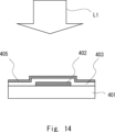
- FIG. 13 and 14 are process cross-sectional views showing the manufacturing process of the semiconductor device.
- a method of manufacturing a semiconductor device having an inverted staggered type TFT will be described.
- 13 and 14 show the process of forming a polysilicon film in the semiconductor manufacturing method. For other manufacturing steps, a known method can be used, so the description is omitted.
- a gate electrode 402 is formed on a glass substrate 401 .
- a gate insulating film 403 is formed on the gate electrode 402 .
- An amorphous silicon film 404 is formed on the gate insulating film 403 .
- the amorphous silicon film 404 is arranged so as to overlap the gate electrode 402 with the gate insulating film 403 interposed therebetween.
- the gate insulating film 403 and the amorphous silicon film 404 are continuously formed by CVD (Chemical Vapor Deposition).
- a polysilicon film 405 is formed as shown in FIG. That is, the amorphous silicon film 404 is dehydrogenated by the laser irradiation apparatus 1 described above. Further, the amorphous silicon film 404 is crystallized by the laser irradiation apparatus 1 of the second and third embodiments. As a result, a polysilicon film 405 of crystallized silicon is formed on the gate insulating film 403 .
- the amorphous silicon film 404 or polysilicon film 405 corresponds to the film 16b described above.
- the laser annealing apparatus irradiates the amorphous silicon film with the laser beam to form the polysilicon film. It may form a microcrystalline silicon film.
- laser light for annealing is not limited to blue laser diodes and Nd:YAG lasers.
- the method according to the present embodiment can also be applied to a laser irradiation apparatus that irradiates a thin film other than a silicon film with a laser beam. That is, the method according to the present embodiment can be applied to any laser irradiation apparatus that forms a crystallized film by irradiating an amorphous film with a laser beam.
- the laser irradiation apparatus 1 can also be applied to laser annealing treatment 2 for dehydrogenating thin films other than silicon films.
- the crystallized film-coated substrate can be appropriately modified.
- the laser irradiation method according to this embodiment is a laser irradiation method for dehydrogenating a film provided on a substrate.
- a laser irradiation method comprises the steps of: generating a blue laser beam with a semiconductor laser light source; guiding the laser beam to a substrate with an optical system unit; and changing the irradiation position of the laser beam with respect to the substrate. I have it.
- Embodiments 1 to 3 can be used in combination as appropriate. It should be noted that the present invention is not limited to the above embodiments, and can be modified as appropriate without departing from the scope of the invention.
Abstract
A laser irradiation device (1) according to an embodiment of the present invention comprises: a laser light source (35); an optical system unit (30) that guides a laser beam (15) to a substrate; a floating unit (10) that has a through-hole provided directly below the position of irradiation with the laser beam (15) and causes the substrate to float; a conveyance unit (11) that conveys the substrate floating on the floating unit (10) in a first direction; and a stage (40) that is disposed on the floating unit (10) and that holds the optical system unit (30) so as to be movable in a second direction different from the first direction in a top view.
Description
本発明はレーザ照射装置、レーザ照射方法、及びディスプレイの製造方法に関する。
The present invention relates to a laser irradiation device, a laser irradiation method, and a display manufacturing method.
特許文献1には、エキシマレーザを用いたレーザアニール装置が開示されている。特許文献1では、浮上ユニットが基板を浮上した状態で、搬送ユニットが基板を搬送している。そして、ライン状のレーザ光が、搬送中の基板に照射される。
Patent Document 1 discloses a laser annealing apparatus using an excimer laser. In Patent Document 1, the transport unit transports the substrate while the floating unit floats the substrate. Then, the substrate being transported is irradiated with the line-shaped laser beam.
このようなエキシマレーザ光源は高価であるため、装置の部品コストを低減することが困難である。したがって、エキシマレーザ光源以外の光源を用いることが望まれる.半導体レーザは、安価であるが、連続発振(CW:Continuous Wave)レーザである。CWレーザ光を変調器でパルス化すると、出力が低下してしまう。よって、多くの光源が必要となり、低コスト化が困難になる。
Since such an excimer laser light source is expensive, it is difficult to reduce the component cost of the device. Therefore, it is desirable to use a light source other than an excimer laser light source. Semiconductor lasers are inexpensive, but continuous wave (CW) lasers. If the CW laser light is pulsed by the modulator, the output will be lowered. Therefore, many light sources are required, making cost reduction difficult.
その他の課題と新規な特徴は、本明細書の記述および添付図面から明らかになるであろう。
Other issues and novel features will become apparent from the description and accompanying drawings of this specification.
一実施の形態によれば、レーザ照射装置は、基板に設けられた膜にレーザ光を照射するレーザ照射装置であって、少なくとも一部が前記膜を透過する波長のレーザ光を発生するレーザ光源と、前記レーザ光を前記基板に導く光学系ユニットと、前記レーザ光の照射位置の直下に設けられた貫通穴を有し、前記基板を浮上させる浮上ユニットと、を備えている。
According to one embodiment, the laser irradiation device is a laser irradiation device that irradiates a film provided on a substrate with a laser beam, and is a laser light source that generates a laser beam having a wavelength at least part of which is transmitted through the film. and an optical system unit that guides the laser beam to the substrate, and a levitation unit that has a through hole provided immediately below the irradiation position of the laser beam and floats the substrate.
一実施の形態によれば、レーザ照射装置は、波長500nm以下のレーザ光を発生する半導体レーザ光源と、基板を第1の方向に搬送する搬送ユニットと、パルス光である前記レーザ光を前記基板に導く光学系ユニットと、上面視において前記第1の方向と異なる第2の方向に、前記基板に対する前記レーザ光の照射位置を変えるよう、前記光学系ユニットを駆動する駆動機構と、を備えている。
According to one embodiment, a laser irradiation apparatus includes a semiconductor laser light source that generates a laser beam having a wavelength of 500 nm or less, a transport unit that transports a substrate in a first direction, and a pulsed laser beam that emits the laser beam to the substrate. and a driving mechanism for driving the optical system unit so as to change the irradiation position of the laser beam with respect to the substrate in a second direction different from the first direction when viewed from above. there is
一実施の形態によれば、レーザ照射装置は、基板に設けられた膜に対して脱水素化処理を行うレーザ照射装置であって、波長500nm以下のレーザ光を発生する半導体レーザ光源と、前記レーザ光を基板に導く光学系ユニットと、前記基板に対する前記レーザ光の照射位置を変化させる駆動機構と、を備えている。
According to one embodiment, the laser irradiation device is a laser irradiation device that dehydrogenates a film provided on a substrate, and includes a semiconductor laser light source that generates a laser beam having a wavelength of 500 nm or less; An optical system unit that guides a laser beam to a substrate and a drive mechanism that changes the irradiation position of the laser beam on the substrate are provided.
一実施の形態によれば、レーザ照射装置は、膜が形成された基板を第1の方向に発生する搬送ユニットと、波長500nm以下のレーザ光を発生する半導体レーザ光源と、前記レーザ光を基板に導く光学系ユニットと、上面視において、前記第1の方向から傾いた第2の方向に、前記基板に対する前記レーザ光の照射位置を変える駆動機構と、前記膜を結晶化させるためのエキシマレーザ光を発生するエキシマレーザ光源と、上面視において前記エキシマレーザ光を前記第1の方向から傾いた方向を長手方向とするライン状のラインビームとして、搬送中の前記基板に導く結晶化用光学系と、を備えている。
According to one embodiment, a laser irradiation apparatus includes a transport unit that generates a substrate on which a film is formed in a first direction, a semiconductor laser light source that generates a laser beam with a wavelength of 500 nm or less, and a substrate that emits the laser beam. a driving mechanism for changing the irradiation position of the laser beam with respect to the substrate in a second direction inclined from the first direction when viewed from above; and an excimer laser for crystallizing the film. an excimer laser light source that generates light; and an optical system for crystallization that guides the excimer laser light to the substrate being transported as a linear line beam having a longitudinal direction inclined from the first direction when viewed from above. and have.
一実施の形態によれば、レーザ照射方法は、基板に設けられた膜にレーザ光を照射するレーザ照射方法であって、(A1)前記レーザ光の照射位置の直下に設けられた貫通穴を有する浮上ユニットによって、前記基板を浮上させるステップと、(A2)少なくとも一部が前記膜を透過する波長のレーザ光を発生するステップと、(A3)光学系ユニットによって前記レーザ光を浮上中の前記基板に導くステップと、を備えている。
According to one embodiment, the laser irradiation method is a laser irradiation method for irradiating a film provided on a substrate with a laser beam, comprising: (A1) a through hole provided immediately below the laser beam irradiation position; (A2) generating a laser beam having a wavelength at least a portion of which is transmitted through the film; leading to the substrate.
一実施の形態によれば、レーザ照射方法は、(B1)半導体レーザ光源によって波長500nm以下のレーザ光を発生するステップと、(B2)搬送ユニットによって、基板を第1の方向に搬送するステップと、(B3)パルス光である前記レーザ光を光学系ユニットによって前記基板に導くステップと、(B4)上面視において前記第1の方向と異なる第2の方向に、前記基板に対する前記レーザ光の照射位置を変えるよう、前記光学系ユニットを駆動するステップと、を備えている。
According to one embodiment, the laser irradiation method includes the steps of (B1) generating laser light with a wavelength of 500 nm or less using a semiconductor laser light source, and (B2) transporting the substrate in a first direction by a transport unit. (B3) guiding the laser light, which is a pulsed light, to the substrate by an optical system unit; and (B4) irradiating the substrate with the laser light in a second direction different from the first direction when viewed from above. and C. driving the optics unit to change position.
一実施の形態によれば、レーザ照射方法は、基板に設けられた膜に対して脱水素化処理を行うレーザ照射方法であって、(C1)半導体レーザ光源によって、波長500nm以下のレーザ光を発生するステップと、(C2)光学系ユニットによって前記レーザ光を基板に導くステップと、(C3)前記基板に対する前記レーザ光の照射位置を変化させるステップと、を備えている。
According to one embodiment, the laser irradiation method is a laser irradiation method for performing a dehydrogenation treatment on a film provided on a substrate, and (C1) emits a laser beam having a wavelength of 500 nm or less from a semiconductor laser light source. (C2) guiding the laser light to the substrate by an optical system unit; and (C3) changing the irradiation position of the laser light on the substrate.
一実施の形態によれば、レーザ照射方法は、(D1)搬送ユニットによって、膜が形成された基板を第1の方向に搬送するステップと、(D2)半導体レーザ光源によって、波長500nm以下のレーザ光を発生するステップと、(D3)光学系ユニットによって、前記レーザ光を基板に導くステップと、(D4)上面視において、前記第1の方向と異なる第2の方向に、前記基板に対する前記レーザ光の照射位置を変えるステップと、(D5)エキシマレーザ光源によって、前記膜を結晶化させるためのエキシマレーザ光を発生するステップと、(D6)上面視において前記エキシマレーザ光を前記第1の方向から傾いた方向を長手方向とするライン状のラインビームとして、搬送中の前記基板に導くステップと、を備えている。
According to one embodiment, the laser irradiation method comprises the steps of: (D1) transporting a substrate having a film formed thereon in a first direction by a transport unit; (D3) guiding the laser beam to the substrate by an optical system unit; (D5) generating an excimer laser beam for crystallizing the film from an excimer laser light source; (D6) directing the excimer laser beam in the first direction when viewed from above; and guiding the light beam to the substrate being transported as a line-shaped line beam whose longitudinal direction is the direction inclined from the vertical direction.
一実施の形態によれば、ディスプレイの製造方法は、(S1)基板上に形成された膜にレーザ光を照射する照射ステップを備え、前記(S1)照射ステップは、(SA1)前記レーザ光の照射位置の直下に設けられた貫通穴を有する浮上ユニットによって、前記基板を浮上させるステップと、(SA2)少なくとも一部が前記膜を透過する波長のレーザ光を発生するステップと、(SA3)光学系ユニットによって前記レーザ光を浮上中の前記基板に導くステップと、を備えている。
According to one embodiment, the display manufacturing method includes (S1) an irradiation step of irradiating a film formed on a substrate with a laser beam, and the (S1) irradiation step includes (SA1) the irradiation of the laser beam. (SA2) generating a laser beam having a wavelength at least partially transmitted through the film; (SA3) optical and guiding the laser light to the floating substrate by a system unit.
一実施の形態によれば、ディスプレイの製造方法は、(S1)基板上に形成された膜にレーザ光を照射する照射ステップを備え、前記(S1)照射ステップは、(SB1)半導体レーザ光源によって波長500nm以下のレーザ光を発生するステップと、(SB2)搬送ユニットによって、基板を第1の方向に搬送するステップと、(SB3)パルス光である前記レーザ光を光学系ユニットによって前記基板に導くステップと、(SB4)上面視において前記第1の方向と異なる第2の方向に、前記基板に対する前記レーザ光の照射位置を変えるよう、前記光学系ユニットを駆動するステップと、を備えている。
According to one embodiment, the display manufacturing method includes (S1) an irradiation step of irradiating a film formed on a substrate with laser light, and the (S1) irradiation step includes (SB1) a semiconductor laser light source. (SB2) transporting a substrate in a first direction by a transport unit; and (SB3) guiding the laser beam, which is pulsed light, to the substrate by an optical system unit. and (SB4) driving the optical system unit so as to change the irradiation position of the laser light on the substrate in a second direction different from the first direction when viewed from above.
一実施の形態によれば、ディスプレイの製造方法は、(T1)基板上に形成された膜に対して脱水素化処理を行うため、前記膜にレーザ光を照射する照射ステップを備え、前記(T1)照射ステップは、(TC1)半導体レーザ光源によって、波長500nm以下のレーザ光を発生するステップと、(TC2)光学系ユニットによって前記レーザ光を基板に導くステップと、(TC3)前記基板に対する前記レーザ光の照射位置を変化させるステップと、を備えている。
According to one embodiment, the display manufacturing method includes (T1) an irradiation step of irradiating the film formed on the substrate with a laser beam in order to dehydrogenate the film, and the ( T1) The irradiating step includes (TC1) generating laser light with a wavelength of 500 nm or less from a semiconductor laser light source, (TC2) guiding the laser light to a substrate by an optical system unit, and (TC3) and changing the irradiation position of the laser light.
一実施の形態によれば、ディスプレイの製造方法は、(S1)基板上に形成された膜にレーザ光を照射する照射ステップを備え、前記(S1)照射ステップは、(SD1)搬送ユニットによって、膜が形成された基板を第1の方向に搬送するステップと、(SD2)半導体レーザ光源によって、波長500nm以下のレーザ光を発生するステップと、(SD3)光学系ユニットによって、前記レーザ光を基板に導くステップと、(SD4)上面視において、前記第1の方向と異なる第2の方向に、前記基板に対する前記レーザ光の照射位置を変えるステップと、(SD5)エキシマレーザ光源によって、前記膜を結晶化させるためのエキシマレーザ光を発生するステップと、(SD6)上面視において前記エキシマレーザ光を前記第1の方向から傾いた方向を長手方向とするライン状のラインビームとして、搬送中の前記基板に導くステップと、を備えている。
According to one embodiment, the display manufacturing method includes (S1) an irradiation step of irradiating a film formed on a substrate with a laser beam, and the (S1) irradiation step includes (SD1) a transport unit, (SD2) generating a laser beam with a wavelength of 500 nm or less using a semiconductor laser light source; (SD4) changing the irradiation position of the laser beam with respect to the substrate in a second direction different from the first direction when viewed from the top; (SD5) exposing the film to the (SD6) generating an excimer laser beam for crystallization; and (SD6) the excimer laser beam being transported as a line-shaped line beam having a longitudinal direction inclined from the first direction when viewed from above. leading to the substrate.
前記一実施の形態によれば、生産性の高いレーザ照射装置、レーザ照射方法、及びディスプレイの製造方法を提供することができる。
According to the embodiment, it is possible to provide a highly productive laser irradiation apparatus, laser irradiation method, and display manufacturing method.
実施の形態1.
本実施の形態にかかるレーザ照射装置は、被処理体(ワークともいう)にレーザ光を照射することでアニール処理を行う。レーザ照射装置は、レーザ光により基板を加熱することで、基板に設けられた膜に対して脱水素化アニール処理を行う。例えば、被処理体は、シリコン膜が形成された膜付き基板となっている。レーザ照射装置は、レーザ光源として、青色半導体レーザ光源を用いている。レーザ照射装置は、半導体レーザ光源からの青色レーザ光を被処理体に照射することで、シリコン膜に対する脱水素処理を行う。なお、レーザ光は青色レーザ光に限らず、波長500nm以下のレーザ光とすることができる。Embodiment 1.
The laser irradiation apparatus according to this embodiment performs annealing by irradiating an object to be processed (also referred to as a work) with a laser beam. The laser irradiation apparatus heats the substrate with laser light to perform dehydrogenation annealing treatment on a film provided on the substrate. For example, the object to be processed is a film-coated substrate on which a silicon film is formed. The laser irradiation device uses a blue semiconductor laser light source as a laser light source. The laser irradiation device irradiates the object to be processed with a blue laser beam from a semiconductor laser light source, thereby performing a dehydrogenation process on the silicon film. Laser light is not limited to blue laser light, and laser light with a wavelength of 500 nm or less can be used.
本実施の形態にかかるレーザ照射装置は、被処理体(ワークともいう)にレーザ光を照射することでアニール処理を行う。レーザ照射装置は、レーザ光により基板を加熱することで、基板に設けられた膜に対して脱水素化アニール処理を行う。例えば、被処理体は、シリコン膜が形成された膜付き基板となっている。レーザ照射装置は、レーザ光源として、青色半導体レーザ光源を用いている。レーザ照射装置は、半導体レーザ光源からの青色レーザ光を被処理体に照射することで、シリコン膜に対する脱水素処理を行う。なお、レーザ光は青色レーザ光に限らず、波長500nm以下のレーザ光とすることができる。
The laser irradiation apparatus according to this embodiment performs annealing by irradiating an object to be processed (also referred to as a work) with a laser beam. The laser irradiation apparatus heats the substrate with laser light to perform dehydrogenation annealing treatment on a film provided on the substrate. For example, the object to be processed is a film-coated substrate on which a silicon film is formed. The laser irradiation device uses a blue semiconductor laser light source as a laser light source. The laser irradiation device irradiates the object to be processed with a blue laser beam from a semiconductor laser light source, thereby performing a dehydrogenation process on the silicon film. Laser light is not limited to blue laser light, and laser light with a wavelength of 500 nm or less can be used.
例えば、ディスプレイパネルの製造工程において、成膜装置が、基板に膜を形成する。そして、レーザ照射装置が膜にレーザ光を照射する。基板は、例えば、ガラス基板や樹脂基板などの透明基板であり、膜は例えば、アモルファスシリコン膜である。アモルファスシリコン膜付きの基板が被処理体となる。レーザ照射装置は、アモルファスシリコン膜にレーザ光を照射することで、アモルファスシリコン膜を脱水素化する。もちろん、被処理体はシリコン膜以外の膜が形成された膜付き基板であってもよい。以下、レーザ照射装置が、レーザ光を用いた脱水素化アニール処理装置であるとして説明を行うが、レーザ照射によりアモルファスシリコン膜を結晶化する結晶化アニール処理装置であってもよい。
For example, in the manufacturing process of a display panel, a film forming device forms a film on a substrate. Then, a laser irradiation device irradiates the film with a laser beam. The substrate is, for example, a transparent substrate such as a glass substrate or a resin substrate, and the film is, for example, an amorphous silicon film. A substrate with an amorphous silicon film is an object to be processed. The laser irradiation device dehydrogenates the amorphous silicon film by irradiating the amorphous silicon film with laser light. Of course, the object to be processed may be a film-coated substrate on which a film other than a silicon film is formed. In the following description, the laser irradiation apparatus is a dehydrogenation annealing apparatus using laser light, but it may be a crystallization annealing apparatus for crystallizing an amorphous silicon film by laser irradiation.
図1~図3を用いて、本実施の形態にかかるレーザ照射装置の構成について説明する。図1は、レーザ照射装置1の構成を模式的に示す上面図ある。図2は、レーザ照射装置1の構成を模式的に示すXZ断面図である。図3は、レーザ照射装置1の構成を模式的に示すYZ断面図である。
The configuration of the laser irradiation apparatus according to this embodiment will be described with reference to FIGS. 1 to 3. FIG. FIG. 1 is a top view schematically showing the configuration of a laser irradiation device 1. FIG. FIG. 2 is an XZ sectional view schematically showing the configuration of the laser irradiation device 1. As shown in FIG. FIG. 3 is a YZ cross-sectional view schematically showing the configuration of the laser irradiation device 1. As shown in FIG.
図1~図3に示すように、レーザ照射装置1は、浮上ユニット10、搬送ユニット11、光学系ユニット30、Y駆動機構32、及びステージ40を備える。浮上ユニット10と搬送ユニット11とが搬送装置を構成する。
As shown in FIGS. 1 to 3, the laser irradiation device 1 includes a levitation unit 10, a transport unit 11, an optical system unit 30, a Y driving mechanism 32, and a stage 40. The levitation unit 10 and the transport unit 11 constitute a transport device.
なお、以下に示す図では、説明の簡略化のため、適宜、XYZ3次元直交座標系を示している。Z方向は鉛直上下方向であり、被処理体16の主面と直交する方向である。X方向は被処理体16の搬送方向である。Y方向は光学系ユニット30の移動方向である。X方向に搬送されている被処理体16に、レーザ光15が照射される。さらに、光学系ユニット30が、Y方向に移動する。したがって、被処理体16に対するレーザ光の照射位置をX方向及びY方向に変化させることができる。これにより、被処理体16のほぼ全面にレーザ光を照射することができる。
It should be noted that the diagrams shown below show an XYZ three-dimensional orthogonal coordinate system as appropriate for simplification of explanation. The Z direction is a vertical up-down direction, and is a direction perpendicular to the main surface of the object 16 to be processed. The X direction is the transport direction of the object 16 to be processed. The Y direction is the moving direction of the optical system unit 30 . A laser beam 15 is applied to an object 16 being transported in the X direction. Furthermore, the optical system unit 30 moves in the Y direction. Therefore, the irradiation position of the laser beam on the object to be processed 16 can be changed in the X direction and the Y direction. As a result, substantially the entire surface of the object 16 to be processed can be irradiated with the laser beam.
図2に示すように、浮上ユニット10は、浮上ユニット10の表面からガスを噴出するように構成されている。浮上ユニット10は、その上面で被処理体16を浮上させる。浮上ユニット10の表面から噴出されたガスが被処理体16の下面に吹き付けられることで、被処理体16が浮上する。被処理体16が搬送される際、浮上ユニット10は被処理体16の上側に配置されている他の機構(不図示)に被処理体16が接触しないように浮上量を調整している。
As shown in FIG. 2, the levitation unit 10 is configured to eject gas from the surface of the levitation unit 10 . The levitation unit 10 levitates the object 16 to be processed on its upper surface. The gas ejected from the surface of the floating unit 10 is sprayed onto the lower surface of the object 16 to float, thereby causing the object 16 to float. When the object 16 to be processed is transported, the floating unit 10 adjusts the floating amount so that the object 16 to be processed does not come into contact with another mechanism (not shown) arranged above the object 16 to be processed.
浮上ユニット10は、多孔質材料によって形成されている。例えば、浮上ユニット10は、多孔質アルミナや多孔質SiC等のセラミック材料で形成されている。ここでは、浮上ユニット10は、厚さ10mmの多孔質材料プレートとなっている。浮上ユニット10は、図示しない給気ポートに接続されている。よって、ガスボンベなどの気体供給手段(不図示)からの気体が浮上ユニット10の上面から噴出される。
The floating unit 10 is made of a porous material. For example, the floating unit 10 is made of a ceramic material such as porous alumina or porous SiC. Here, the levitation unit 10 is a porous material plate with a thickness of 10 mm. The floating unit 10 is connected to an air supply port (not shown). Therefore, gas from a gas supply means (not shown) such as a gas cylinder is jetted out from the upper surface of the levitation unit 10 .
搬送ユニット11は、浮上している被処理体16を搬送方向に搬送する。図1に示すように、搬送ユニット11は、保持機構12と移動機構13とを備える。保持機構12は、被処理体16を保持する。例えば、保持機構12は、真空吸着機構を用いて構成することができる。真空吸着機構はアルミニウム合金などの金属材料により形成されている。あるいは、保持機構12は、PEEK(ポリエーテルエーテルケトン)材などの樹脂系材料で形成されていてもよい。保持機構12の上面には、吸着溝や吸着穴等が形成されている。保持機構12は多孔質材料で形成されていても良い。
The transport unit 11 transports the floating object to be processed 16 in the transport direction. As shown in FIG. 1 , the transport unit 11 has a holding mechanism 12 and a moving mechanism 13 . The holding mechanism 12 holds the object 16 to be processed. For example, the holding mechanism 12 can be configured using a vacuum suction mechanism. The vacuum adsorption mechanism is made of metal material such as aluminum alloy. Alternatively, the holding mechanism 12 may be made of a resin-based material such as PEEK (polyetheretherketone) material. A suction groove, a suction hole, and the like are formed on the upper surface of the holding mechanism 12 . The holding mechanism 12 may be made of a porous material.
保持機構12(真空吸着機構)は、排気ポート(不図示)に接続されており、排気ポートはエジェクタや真空ポンプなどに接続されている。よって、保持機構12にはガスを吸引するための負圧が作用するため、保持機構12を用いて被処理体16を保持することができる。
The holding mechanism 12 (vacuum suction mechanism) is connected to an exhaust port (not shown), and the exhaust port is connected to an ejector, a vacuum pump, and the like. Therefore, since a negative pressure for sucking gas acts on the holding mechanism 12 , the object to be processed 16 can be held using the holding mechanism 12 .
保持機構12は、被処理体16のレーザ光15が照射される面(上面)と逆側の面(下面)、つまり、被処理体16の浮上ユニット10と対向する側の面を吸引することで、被処理体16を保持している。また、保持機構12は、被処理体16の+Y方向における端部を保持している。
The holding mechanism 12 sucks the surface (lower surface) of the object 16 to be processed that is opposite to the surface (upper surface) irradiated with the laser beam 15 , that is, the surface of the object 16 to be processed that faces the levitation unit 10 . and holds the object 16 to be processed. In addition, the holding mechanism 12 holds the +Y-direction end of the object 16 to be processed.
搬送ユニット11が備える移動機構13は保持機構12と連結されている。移動機構13は、保持機構12を搬送方向に移動可能に構成されている。搬送ユニット11(保持機構12及び移動機構13)は、浮上ユニット10の+Y方向の端部側に設けられており、保持機構12で被処理体16を保持しつつ、移動機構13が搬送方向に移動することで被処理体16が搬送される。
A moving mechanism 13 provided in the transport unit 11 is connected to the holding mechanism 12 . The moving mechanism 13 is configured to move the holding mechanism 12 in the transport direction. The transport unit 11 (holding mechanism 12 and moving mechanism 13) is provided on the +Y-direction end side of the levitation unit 10. While the holding mechanism 12 holds the object to be processed 16, the moving mechanism 13 moves in the transport direction. The object to be processed 16 is conveyed by moving.
図1に示すように、例えば、移動機構13は浮上ユニット10の+Y方向の端部を搬送方向に沿ってスライドするように構成されている。移動機構13が浮上ユニット10の端部を搬送方向に沿ってスライドすることで、被処理体16が搬送方向に沿って搬送される。
As shown in FIG. 1, for example, the moving mechanism 13 is configured to slide the end of the levitation unit 10 in the +Y direction along the transport direction. The moving mechanism 13 slides the end of the levitation unit 10 along the transport direction, thereby transporting the workpiece 16 along the transport direction.
移動機構13の移動速度を制御することで、被処理体16の搬送速度を制御することができる。移動機構13は、例えば、図示しないモータなどのアクチュエータとリニアガイド機構やエアベアリング等を備えている。
By controlling the moving speed of the moving mechanism 13, the transport speed of the object 16 to be processed can be controlled. The moving mechanism 13 includes, for example, an actuator such as a motor (not shown), a linear guide mechanism, an air bearing, and the like.
被処理体16はX方向及びY方向と平行な端辺を有する矩形基板となっている。被処理体16は、基板16aと、基板16a上に形成された膜16bを備えている。基板16aはガラス基板などの透明基板である。膜16bは、アモルファスシリコン膜などのシリコン膜である。膜16bにレーザ光15を照射してアニール処理することで、膜16bに含まれる水素を抜くことができる。つまり、レーザ照射装置1は、脱水素化処理装置となる。なお、シリコン膜である膜16bが示されているが、その他の膜が形成されていても良い。例えば、シリコン膜の下地膜として、配線などとなる銅やアルミニウムの薄膜が形成されていてもよい。さらには、基板16aには、酸化シリコン膜などの絶縁膜が下地膜として形成されていてもよい。
The object 16 to be processed is a rectangular substrate having edges parallel to the X direction and the Y direction. The object 16 to be processed includes a substrate 16a and a film 16b formed on the substrate 16a. The substrate 16a is a transparent substrate such as a glass substrate. Film 16b is a silicon film, such as an amorphous silicon film. By irradiating the film 16b with the laser light 15 for annealing, hydrogen contained in the film 16b can be removed. That is, the laser irradiation device 1 serves as a dehydrogenation device. Although the film 16b, which is a silicon film, is shown, other films may be formed. For example, a thin film of copper or aluminum that serves as wiring may be formed as a base film of the silicon film. Furthermore, an insulating film such as a silicon oxide film may be formed on the substrate 16a as a base film.
浮上ユニット10の上方には、ステージ40が配置されている。ステージ40は、光学系ユニット30を移動可能に保持している。光学系ユニット30は、レーザ光源35からのレーザ光を被処理体16に導く。光学系ユニット30は、ステージ40よりも-X側に配置されている。したがって、光学系ユニット30は被処理体16の真上に配置されている。よって、光学系ユニット30からのレーザ光15が上側から被処理体16に照射される。
A stage 40 is arranged above the levitation unit 10 . The stage 40 movably holds the optical system unit 30 . The optical system unit 30 guides the laser light from the laser light source 35 to the object 16 to be processed. The optical system unit 30 is arranged on the −X side of the stage 40 . Therefore, the optical system unit 30 is arranged directly above the object 16 to be processed. Therefore, the object to be processed 16 is irradiated with the laser beam 15 from the optical system unit 30 from above.
ステージ40は光学系ユニット30のY方向の移動をガイドするガイド機構となる。例えば、ステージ40にはガイドレールやガイド溝などが設けられている。また、ステージ40には、Y駆動機構32が設けられている。ステージ40は、浮上ユニット10の上方の空間において、Y方向に沿って設けられたガントリーステージである。Y駆動機構32が光学系ユニット30をY方向に駆動する。
The stage 40 serves as a guide mechanism that guides the movement of the optical system unit 30 in the Y direction. For example, the stage 40 is provided with guide rails, guide grooves, and the like. A Y drive mechanism 32 is also provided on the stage 40 . The stage 40 is a gantry stage provided along the Y direction in the space above the levitation unit 10 . A Y drive mechanism 32 drives the optical system unit 30 in the Y direction.
光学系ユニット30がステージ40に沿って移動する。光学系ユニット30がY方向に移動するため、レーザ光15の照射位置がY方向に変化する。+Y側及び-Y側において、ステージ40は浮上ユニット10からはみ出すように配置されている。従って、Y方向において、光学系ユニット30は、被処理体16の任意の位置にレーザ光を照射することができる。
The optical system unit 30 moves along the stage 40. Since the optical system unit 30 moves in the Y direction, the irradiation position of the laser beam 15 changes in the Y direction. The stage 40 is arranged to protrude from the levitation unit 10 on the +Y side and the -Y side. Therefore, in the Y direction, the optical system unit 30 can irradiate laser light to any position on the object 16 to be processed.
次に、レーザ光源とその光学系の一例について説明する。レーザ光源35は、被処理体16をアニールするためのレーザ光を発生する。レーザ光源35は、中心波長450nmの青色レーザ光を発生するBLD(Blue Laser Diode)である。つまり、レーザ光源35は青色半導体レーザ光源である。ここで、レーザ光は連続発振のCW(Continuous Wave)レーザ光となっている。もちろん、レーザ照射装置1は、変調器などを用いて、レーザ光をパルスレーザ光に変調しても良い。
Next, an example of a laser light source and its optical system will be described. The laser light source 35 generates laser light for annealing the object 16 to be processed. The laser light source 35 is a BLD (Blue Laser Diode) that generates blue laser light with a central wavelength of 450 nm. That is, the laser light source 35 is a blue semiconductor laser light source. Here, the laser light is a continuous wave (CW) laser light. Of course, the laser irradiation device 1 may use a modulator or the like to modulate the laser light into a pulsed laser light.
レーザ光源35は、光ファイバ36に結合されている。レーザ光源35からのレーザ光は、光ファイバ36を介して、光学系ユニット30に入射する。図2に示されるように、光学系ユニット30は、レンズ301、ミラー302,及びレンズ303を備えている。もちろん、光学系ユニット30にはレンズ301、ミラー302、レンズ303以外の光学素子が設けられていても良い。また、被処理体16において、レーザ光15のスポット形状が10mm×0.3mmのライン状となっている。レーザ光15がCW光であり、被処理体16の1点における照射時間は10μsec~1secとする。
A laser light source 35 is coupled to an optical fiber 36 . Laser light from the laser light source 35 enters the optical system unit 30 via the optical fiber 36 . As shown in FIG. 2, the optical system unit 30 has a lens 301, a mirror 302, and a lens 303. As shown in FIG. Of course, the optical system unit 30 may be provided with optical elements other than the lens 301 , the mirror 302 and the lens 303 . Also, on the object 16 to be processed, the spot shape of the laser beam 15 is a line shape of 10 mm×0.3 mm. The laser light 15 is CW light, and the irradiation time at one point on the object 16 to be processed is set to 10 μsec to 1 sec.
光ファイバ36からのレーザ光は、レンズ301に入射する。レンズ301で集光されたレーザ光は、ミラー302に入射する。ミラー302はレーザ光を被処理体16に向けて反射する。具体的には、ミラー302はレーザ光を下方に反射する。ミラー302で反射されたレーザ光は、レンズ303に入射する。
A laser beam from the optical fiber 36 enters the lens 301 . A laser beam condensed by the lens 301 is incident on the mirror 302 . The mirror 302 reflects the laser light toward the object 16 to be processed. Specifically, the mirror 302 reflects the laser light downward. The laser beam reflected by the mirror 302 enters the lens 303 .
レンズ303からのレーザ光15が被処理体16に照射される。レンズ303は、レーザ光15を被処理体16に集光する。よって、光学系ユニット30からのレーザ光15は集束ビームとなって、被処理体16に照射される。光学系ユニット30は、上方からレーザ光15を被処理体16に照射する。被処理体16の膜16bがアニールされ、膜16bに対して脱水素化処理を行うことができる。なお、レンズ303の光軸はZ方向と平行になっているが、Z方向から傾いていてもよい。
The object 16 to be processed is irradiated with the laser beam 15 from the lens 303 . The lens 303 converges the laser beam 15 onto the object 16 to be processed. Therefore, the laser beam 15 from the optical system unit 30 becomes a converging beam and is irradiated onto the object 16 to be processed. The optical system unit 30 irradiates the object 16 to be processed with the laser beam 15 from above. The film 16b of the object 16 to be processed is annealed, and dehydrogenation treatment can be performed on the film 16b. Although the optical axis of the lens 303 is parallel to the Z direction, it may be tilted from the Z direction.
ここで、レーザ光源35が青色の半導体レーザ光源であるため、レーザ光15が青色レーザ光となっている。例えば、レーザ光15の中心波長は450nmとなっている。青色の光はシリコン膜に対する浸透深さが深い。よって、レーザ光15の全てが被処理体16で吸収されずに、レーザ光15の一部が被処理体16を透過してしまう。
Here, since the laser light source 35 is a blue semiconductor laser light source, the laser light 15 is blue laser light. For example, the center wavelength of the laser light 15 is 450 nm. Blue light has a deep penetration depth into the silicon film. Therefore, not all of the laser beam 15 is absorbed by the object 16 to be processed, and part of the laser beam 15 is transmitted through the object 16 to be processed.
ここで、被処理体16を透過したレーザ光が浮上ユニット10で吸収されると、浮上ユニット10が加熱されてしまう。よって、プロセス中に、浮上ユニット10の温度が変動してしまう。さらに、浮上ユニット10の表面でレーザ光が反射又は散乱されてしまうため、照射箇所の直下からのレーザ光が再度、被処理体16に入射してしまう。したがって、脱水素化のアニールプロセスが不安定になってしまうおそれがある。
Here, if the laser beam transmitted through the object 16 to be processed is absorbed by the levitation unit 10, the levitation unit 10 is heated. Therefore, the temperature of the levitation unit 10 fluctuates during the process. Furthermore, since the laser light is reflected or scattered on the surface of the levitation unit 10 , the laser light from directly below the irradiated portion enters the object 16 to be processed again. Therefore, the annealing process for dehydrogenation may become unstable.
そこで、本実施の形態では、図1,図2に示すように、レーザ光15の照射箇所の直下において、浮上ユニット10に貫通穴10aを設けている。上面視において、貫通穴10aはY方向を長手方向とする帯状の領域に形成されている。レーザ光15は、貫通穴10aを通過するため、浮上ユニット10に入射しない。浮上ユニット10でレーザ光15が吸収、反射又は散乱されるのを防ぐことができる。X方向において、貫通穴10aの幅は10mm程度になっている。Y方向において、貫通穴10aの長さは、光学系ユニット30の可動範囲と同程度になっている。
Therefore, in the present embodiment, as shown in FIGS. 1 and 2, the levitation unit 10 is provided with a through hole 10a directly below the irradiation location of the laser beam 15. FIG. When viewed from above, the through hole 10a is formed in a belt-like region having the Y direction as the longitudinal direction. The laser beam 15 does not enter the levitation unit 10 because it passes through the through hole 10a. Absorption, reflection or scattering of the laser light 15 in the levitation unit 10 can be prevented. The width of the through hole 10a in the X direction is about 10 mm. The length of the through hole 10 a in the Y direction is approximately the same as the movable range of the optical system unit 30 .
これにより、浮上ユニット10の温度を安定化することができる。さらに、浮上ユニット10からの反射光又は散乱光が被処理体16に再度入射することを防ぐことができる。浮上ユニット10の表面からの反射光及び散乱光を低減することができる。このようにすることで、安定した脱水素化プロセスが可能になり、生産性を向上することができる。
Thereby, the temperature of the levitation unit 10 can be stabilized. Furthermore, it is possible to prevent reflected light or scattered light from the floating unit 10 from entering the object 16 again. Reflected light and scattered light from the surface of the levitation unit 10 can be reduced. By doing so, a stable dehydrogenation process becomes possible, and productivity can be improved.
また、本実施の形態では、搬送ユニット11が被処理体16を搬送中に、Y駆動機構32が光学系ユニット30を駆動している。つまり、Y駆動機構32によってレーザ光の照射位置がY方向に移動するとともに、搬送ユニット11によって被処理体16がX方向に移動している。したがって、被処理体16に対するレーザ光の照射位置がX方向及びY方向に変化する。これにより、被処理体16のほぼ全面にレーザ光を照射することができる。よって、膜16bのほぼ全体をアニールすることができ、脱水素化処理を適切に行うことができる。
Further, in the present embodiment, the Y drive mechanism 32 drives the optical system unit 30 while the transport unit 11 transports the object 16 to be processed. That is, the Y drive mechanism 32 moves the irradiation position of the laser beam in the Y direction, and the transport unit 11 moves the object 16 to be processed in the X direction. Therefore, the irradiation position of the laser beam on the object to be processed 16 changes in the X direction and the Y direction. As a result, substantially the entire surface of the object 16 to be processed can be irradiated with the laser beam. Therefore, almost the entire film 16b can be annealed, and the dehydrogenation treatment can be appropriately performed.
また、Y方向における光学系ユニット30の移動速度が、X方向の搬送速度よりも速くなっていても良い。このようにすることで、Y方向において、レーザ照射位置を高速に変化させることができる。よって、局所的な加熱を防ぐことができるため、下地膜などに対する影響を防ぐことができる。
Also, the moving speed of the optical system unit 30 in the Y direction may be faster than the transport speed in the X direction. By doing so, the laser irradiation position can be changed at high speed in the Y direction. Therefore, since local heating can be prevented, an influence on a base film or the like can be prevented.
なお、本実施の形態ではレーザ光源35として、青色レーザダイオードが設けられているが、レーザ光源35はこれに限られるものではない。具体的には、レーザ光源35は、基板16a上に所定の厚さの膜16bが設けられている場合、レーザ光の少なくとも一部が膜16bを透過する波長のレーザ光を発生するものであればよい。
Although a blue laser diode is provided as the laser light source 35 in this embodiment, the laser light source 35 is not limited to this. Specifically, when a film 16b having a predetermined thickness is provided on the substrate 16a, the laser light source 35 may generate laser light having a wavelength that at least part of the laser light passes through the film 16b. Just do it.
膜16bを透過する波長か否かは、膜の材質や厚さに応じて決まる。例えば、膜16bがアモルファスシリコン膜である場合、波長450nmの光に対する浸透深さ(進入深さ)は0.02μmとなる。浸透深さは、物質に入射した入射光の光量が1/eになるときの物質の厚さである。eはネイピア数である。浸透深さは物質の消衰係数で決まる。また、消衰係数は、波長依存性がある。浸透深さは膜の材質、および光の波長によって決まる。
Whether or not the wavelength is transmitted through the film 16b is determined according to the material and thickness of the film. For example, if the film 16b is an amorphous silicon film, the penetration depth (penetration depth) for light with a wavelength of 450 nm is 0.02 μm. The penetration depth is the thickness of a material when the amount of light incident on the material becomes 1/e. e is the Napier number. The penetration depth is determined by the material's extinction coefficient. Also, the extinction coefficient is wavelength dependent. The depth of penetration is determined by the material of the membrane and the wavelength of the light.
図4は、アモルファスシリコン(a-Si)膜と、単結晶シリコン(c-Si)膜の浸透深さを示す表である。図4では、波長が308nm、355nm、450nm、532nm、808nmの光に対する浸透深さが示されている。浸透深さは、吸収率が1/e(63%)になるときの膜厚となる。膜16bがアモルファスシリコン膜であり、レーザ波長が450nmとすると、浸透深さは0.02μmとなる。換言すると、波長450nmのレーザ光が膜厚0.02μmのアモルファスシリコン膜を入射すると、36.8%がアモルファスシリコン膜を透過し、1/e=63%がアモルファスシリコン膜で吸収される。
FIG. 4 is a table showing penetration depths of an amorphous silicon (a-Si) film and a single crystal silicon (c-Si) film. FIG. 4 shows the penetration depth for light with wavelengths of 308 nm, 355 nm, 450 nm, 532 nm and 808 nm. The penetration depth is the film thickness when the absorptance becomes 1/e (63%). If the film 16b is an amorphous silicon film and the laser wavelength is 450 nm, the penetration depth is 0.02 μm. In other words, when laser light with a wavelength of 450 nm is incident on an amorphous silicon film with a thickness of 0.02 μm, 36.8% is transmitted through the amorphous silicon film and 1/e=63% is absorbed by the amorphous silicon film.
膜16bが浸透深さの4倍の膜厚を有する場合、レーザ光の1.8%(=1/e4)が膜16bを透過することになる。また、脱水素化のためのアニールプロセスにおいて、レーザ光の1.8%が浮上ユニット10に入射するとアニールプロセスに影響が生じてしまう。したがって、本実施の形態に係るレーザ照射装置1は、浸透深さの4倍以下の膜厚を有する膜16bのアニールに好適である。換言すると、浸透深さの4倍以上の膜厚を有する膜をアニールする場合、浮上ユニット10に対する影響が軽微である。膜16bの膜厚が決まっていれば、本実施の形態に好適なレーザ波長の範囲が決まる。
If the film 16b has a thickness of four times the penetration depth, 1.8% (=1/e 4 ) of the laser light will pass through the film 16b. Also, in the annealing process for dehydrogenation, if 1.8% of the laser light enters the floating unit 10, the annealing process will be affected. Therefore, the laser irradiation apparatus 1 according to the present embodiment is suitable for annealing the film 16b having a film thickness of four times or less the penetration depth. In other words, when annealing a film having a film thickness greater than four times the penetration depth, the effect on the levitation unit 10 is minor. If the thickness of the film 16b is determined, the range of laser wavelength suitable for this embodiment is determined.
ここで、膜16bが厚さ40nmのアモルファスシリコン膜であるとする。図4の表に示す通り、レーザ波長が355nmの時の浸透深さは10nmである。レーザ波長が355nm以上の時に、レーザ光の2%以上が膜16bを透過して、プロセスに影響が生じてしまう。例えば、355nm以上808nm以下のレーザ波長のレーザ光を用いた場合、2%以上のレーザ光が膜16bを透過してしまう。浮上ユニット10での吸収、反射、又は散乱は、プロセスばらつきの原因となるおそれがある。よって、本実施の形態に係るレーザ照射装置は、355nm以上、808nm以下の波長のレーザ光を用いた場合に好適である。つまり、レーザ波長の光の浸透深さの4倍以下の膜厚を有する膜のアニールに好適である。
Here, it is assumed that the film 16b is an amorphous silicon film with a thickness of 40 nm. As shown in the table of FIG. 4, the penetration depth is 10 nm when the laser wavelength is 355 nm. When the laser wavelength is 355 nm or more, 2% or more of the laser light is transmitted through the film 16b, which affects the process. For example, when laser light with a laser wavelength of 355 nm or more and 808 nm or less is used, 2% or more of the laser light passes through the film 16b. Absorption, reflection, or scattering at the levitation unit 10 can cause process variations. Therefore, the laser irradiation apparatus according to this embodiment mode is suitable when laser light with a wavelength of 355 nm or more and 808 nm or less is used. That is, it is suitable for annealing a film having a film thickness four times or less the penetration depth of light of a laser wavelength.
なお、本実施の形態において、光学系ユニット30は、レーザ光を走査するための光スキャナを有していてもよい。例えば、ミラー302がガルバノミラーであってもよい。光スキャナは、レーザ光を偏向することで、レーザ光の照射位置が変化する。ここで、光スキャナは、レーザ光の照射位置をX方向に変化させる1軸の光スキャナとなっている。つまり、光スキャナがX方向に照射位置を変化させることで、被処理体16の1点にレーザ光が連続的に照射される照射時間を短くすることできる。これにより、下地膜などの局所的な加熱を防ぐことができる。よって、安定したアニールプロセスが可能になる。光スキャナを用いる場合、レンズ303はfθレンズであってもよい。これにより、光スキャナがレーザ光を偏向した場合でも、レーザ光の照射方向をZ方向と平行にすることができる。
Note that in the present embodiment, the optical system unit 30 may have an optical scanner for scanning laser light. For example, mirror 302 may be a galvanometric mirror. The optical scanner changes the irradiation position of the laser light by deflecting the laser light. Here, the optical scanner is a uniaxial optical scanner that changes the irradiation position of the laser light in the X direction. That is, by changing the irradiation position of the optical scanner in the X direction, it is possible to shorten the irradiation time during which one point of the object 16 to be processed is continuously irradiated with the laser beam. This can prevent local heating of the base film or the like. Therefore, a stable annealing process becomes possible. If an optical scanner is used, lens 303 may be an f-theta lens. Thereby, even when the optical scanner deflects the laser light, the irradiation direction of the laser light can be made parallel to the Z direction.
本実施の形態にかかるレーザ照射方法は、基板に設けられた膜にレーザ光を照射するレーザ照射方法である。レーザ照射方法は、レーザ光の照射位置の直下に設けられた貫通穴を有する浮上ユニットによって、前記基板を浮上させるステップと、前記浮上ユニット上を浮上している前記基板を第1の方向に搬送するステップと、少なくとも一部が前記膜を透過する波長のレーザ光を発生するステップと、光学系ユニットによって前記レーザ光を搬送中の前記基板に導くステップと、上面視において、前記第1の方向と異なる第2の方向にレーザ光の照射位置を変えるように、前記光学系ユニットを第2の方向に移動させるステップと、を備えている。これにより、生産性を向上することができる。
A laser irradiation method according to the present embodiment is a laser irradiation method for irradiating a film provided on a substrate with laser light. The laser irradiation method comprises the steps of: floating the substrate by a floating unit having a through hole provided immediately below a laser beam irradiation position; and transporting the substrate floating on the floating unit in a first direction. generating a laser beam having a wavelength at least part of which is transmitted through the film; guiding the laser beam to the substrate being transported by an optical system unit; and moving the optical system unit in a second direction so as to change the irradiation position of the laser light in a second direction different from the above. Thereby, productivity can be improved.
(変形例1)
変形例1にかかるレーザ照射装置1について、図5を用いて説明する。図5は、レーザ照射装置1の構成を模式的に示す側面断面図である。変形例1では、実施の形態1の構成に対して、ダンパ19が追加されている。 (Modification 1)
Alaser irradiation device 1 according to Modification 1 will be described with reference to FIG. FIG. 5 is a side sectional view schematically showing the configuration of the laser irradiation device 1. As shown in FIG. In modification 1, a damper 19 is added to the configuration of the first embodiment.
変形例1にかかるレーザ照射装置1について、図5を用いて説明する。図5は、レーザ照射装置1の構成を模式的に示す側面断面図である。変形例1では、実施の形態1の構成に対して、ダンパ19が追加されている。 (Modification 1)
A
ダンパ19は貫通穴10aの直下に配置されている。ダンパ19は、貫通穴10aを通過したレーザ光15を吸収する。ダンパ19は、Y方向と長手方向とする金属ブロックである。貫通穴10aと同程度の長さとすることができる。例えば、ダンパ19は黒色に着色された金属材料等で形成されている。レーザ光15を吸収するダンパ19を設けることで、貫通穴10aの周辺で反射又は散乱されたレーザ光が被処理体16に入射することができる。これにより、より安定したプロセスが可能になる。
The damper 19 is arranged directly below the through hole 10a. The damper 19 absorbs the laser beam 15 that has passed through the through hole 10a. The damper 19 is a metal block whose longitudinal direction is the Y direction. The length can be approximately the same as that of the through hole 10a. For example, the damper 19 is made of a metallic material or the like colored black. By providing the damper 19 that absorbs the laser beam 15 , the laser beam reflected or scattered around the through hole 10 a can enter the object 16 to be processed. This allows for a more stable process.
なお、図5では、ダンパ19が、貫通穴10aの直下に配置されているが、ダンパ19の配置箇所は、貫通穴10aの直下に限定されるものではない。例えば、貫通穴10aの直下には、青色レーザ光を反射するミラー等を配置してもよい。ダンパ19はミラーで反射されたレーザ光を吸収できる位置に配置されていればよい。つまり、ダンパ19が、ミラーで反射した青色レーザ光を吸収する。
Although the damper 19 is arranged directly below the through-hole 10a in FIG. 5, the arrangement location of the damper 19 is not limited to directly below the through-hole 10a. For example, a mirror or the like that reflects the blue laser light may be arranged directly below the through hole 10a. The damper 19 may be arranged at a position where it can absorb the laser beam reflected by the mirror. That is, the damper 19 absorbs the blue laser light reflected by the mirror.
ダンパ19は、冷却されていてもよい。例えば、空冷機構や水冷機構の冷却機構がダンパ19に設けられていても良い。あるいは、ダンパ19には、放熱機構が設けられていてもよい。このようにすることで、ダンパ19とその周辺の温度上昇を抑制することができるため、安定してアニールプロセスを実行することができる。
The damper 19 may be cooled. For example, the damper 19 may be provided with a cooling mechanism such as an air cooling mechanism or a water cooling mechanism. Alternatively, the damper 19 may be provided with a heat dissipation mechanism. By doing so, the temperature rise of the damper 19 and its surroundings can be suppressed, so that the annealing process can be performed stably.
実施の形態2.
実施の形態2にかかるレーザ照射装置について、図6を用いて説明する。図6は、レーザ照射装置1の構成を模式的に示す断面図である。実施の形態2では、レーザ照射装置1が、アモルファスシリコン膜を結晶化するためのレーザ結晶化装置となっている。ここで、レーザ光照射前の膜16bはアモルファスシリコン膜となっている。レーザ光照射後の膜16bはポリシリコン膜となっている。レーザ光源35が青色半導体レーザ光源である。青色レーザ光を照射することで、膜16bがポリシリコン膜となる。Embodiment 2.
A laser irradiation apparatus according to a second embodiment will be described with reference to FIG. FIG. 6 is a cross-sectional view schematically showing the configuration of thelaser irradiation device 1. As shown in FIG. In Embodiment 2, the laser irradiation device 1 is a laser crystallization device for crystallizing an amorphous silicon film. Here, the film 16b before laser light irradiation is an amorphous silicon film. The film 16b after laser light irradiation is a polysilicon film. A laser light source 35 is a blue semiconductor laser light source. By irradiating the blue laser light, the film 16b becomes a polysilicon film.
実施の形態2にかかるレーザ照射装置について、図6を用いて説明する。図6は、レーザ照射装置1の構成を模式的に示す断面図である。実施の形態2では、レーザ照射装置1が、アモルファスシリコン膜を結晶化するためのレーザ結晶化装置となっている。ここで、レーザ光照射前の膜16bはアモルファスシリコン膜となっている。レーザ光照射後の膜16bはポリシリコン膜となっている。レーザ光源35が青色半導体レーザ光源である。青色レーザ光を照射することで、膜16bがポリシリコン膜となる。
A laser irradiation apparatus according to a second embodiment will be described with reference to FIG. FIG. 6 is a cross-sectional view schematically showing the configuration of the
レーザ照射装置1が、変調器306、及びビーム成形部307を備えている。変調器306、及びビーム成形部307は光学系ユニット30に搭載されている。変調器306、ビーム成形部307以外の構成については、実施の形態1と同様であるため説明を省略する。
The laser irradiation device 1 has a modulator 306 and a beam shaping section 307 . The modulator 306 and beam shaping section 307 are mounted on the optical system unit 30 . Configurations other than the modulator 306 and the beam shaping section 307 are the same as those in the first embodiment, so description thereof will be omitted.
変調器306は、レーザ光を変調する。これにより、CWレーザ光がパルスレーザ光に変調される。ここでは、パルスレーザ光の繰り返し周波数Rが、10kHz~200kHzとなっている。レーザ光が被処理体16の1箇所に連続して照射される照射時間は、1μsec以下とすることが好ましい。
A modulator 306 modulates the laser light. This modulates the CW laser light into pulsed laser light. Here, the repetition frequency R of the pulsed laser light is 10 kHz to 200 kHz. It is preferable that the irradiation time during which the laser beam is continuously irradiated to one location of the object 16 to be processed is 1 μsec or less.
変調器306からのパルスレーザ光は、ビーム成形部307に入射する。ビーム成形部307が、パルスレーザ光のスポット形状を成形する。例えば、ビーム成形部307は、スリットなどのビーム成形機構を有している。あるいは、複数本の光ファイバ36を用いている場合、光ファイバ36の出射端の配置によりビームを成形してもよい。ビーム成形部307は、光軸と直交する方向のビーム断面形状(スポット形状)が矩形状になるように、ビームを成形する。例えば、スポット形状は、長手方向のサイズが10mm、短手方向のサイズが0,03mmの矩形状となる。なお、被処理体16におけるビームのスポット形状については後述する。
The pulsed laser light from the modulator 306 enters the beam shaping section 307 . A beam shaping section 307 shapes the spot shape of the pulsed laser light. For example, the beam shaping section 307 has a beam shaping mechanism such as a slit. Alternatively, if multiple optical fibers 36 are used, the beam may be shaped by the placement of the output ends of the optical fibers 36 . The beam shaping section 307 shapes the beam so that the beam cross-sectional shape (spot shape) in the direction perpendicular to the optical axis is rectangular. For example, the shape of the spot is rectangular with a size of 10 mm in the longitudinal direction and a size of 0.03 mm in the lateral direction. The spot shape of the beam on the object to be processed 16 will be described later.
ビーム成形部307で成形されたパルスレーザ光は、実施の形態1と同様に、レンズ301、ミラー302及びレンズ303を介して、被処理体16に入射される。ここで、被処理体16におけるビームのスポット形状を図7に示す。
The pulsed laser light shaped by the beam shaping unit 307 is incident on the object to be processed 16 via the lens 301, the mirror 302 and the lens 303, as in the first embodiment. Here, FIG. 7 shows the beam spot shape on the object 16 to be processed.
図7は、被処理体16におけるパルスレーザ光のスポット形状を模式的に示すXY平面図である。なお、以下の説明では、搬送ユニット11による被処理体16の搬送速度がY駆動機構32による光学系ユニット30の移動速度よりも十分に遅いものとして説明する。なお、以下に示すサイズなどは本実施形態の一例であり、本実施形態は以下のサイズに限られるものではない。
FIG. 7 is an XY plan view schematically showing the spot shape of the pulsed laser beam on the object 16 to be processed. In the following description, it is assumed that the transportation speed of the object to be processed 16 by the transportation unit 11 is sufficiently slower than the moving speed of the optical system unit 30 by the Y drive mechanism 32 . Note that the sizes and the like shown below are examples of the present embodiment, and the present embodiment is not limited to the following sizes.
被処理体16におけるレーザ光15のスポット形状は、長手方向を有する矩形状となっている。例えば、スポット形状の長手方向のサイズLが900μmとなっており、短手方向のサイズが、15μmとなっている。短手方向と長手方向は直交する方向である。そして、長手方向がX方向及びY方向から傾いている。具体的には、短手方向とY方向の成す角度θが45°となっている。つまり、スポット形状の長手方向は、光学系ユニット30の移動方向から45°傾いた方向になっている。
The shape of the spot of the laser beam 15 on the object 16 to be processed is rectangular with a longitudinal direction. For example, the size L of the spot shape in the longitudinal direction is 900 μm, and the size in the lateral direction is 15 μm. The lateral direction and the longitudinal direction are directions orthogonal to each other. And the longitudinal direction is inclined from the X direction and the Y direction. Specifically, the angle θ between the lateral direction and the Y direction is 45°. That is, the longitudinal direction of the spot shape is slanted by 45° from the moving direction of the optical system unit 30 .
また、光学系ユニット30のY方向における移動速度Vが70.7mm/sとなっている。パルスレーザ光の繰り返し周波数R=10kHzである。したがって、Y方向において、1パルス当たりの照射位置のずれ量Pは7.07μm/Pulseである。つまり、連続する2つのパルスレーザ光15aとパルスレーザ光15bの照射位置(ショット位置)がY方向に7.07μmずれている。
Also, the moving speed V of the optical system unit 30 in the Y direction is 70.7 mm/s. The repetition frequency of the pulsed laser light is R=10 kHz. Therefore, in the Y direction, the displacement amount P of the irradiation position per pulse is 7.07 μm/pulse. That is, the irradiation positions (shot positions) of the two consecutive pulse laser beams 15a and 15b are shifted in the Y direction by 7.07 μm.
スポット形状の長手方向におけるパルスレーザ光15a、15bの照射位置のずれ量D(=P×sinθ)は5μmとなる。スポット形状の短手方向におけるパルスレーザ光15a、15bの照射位置のずれ量H(=P×cosθ)は5μmとなる。また、S(=L×sinθ)は、318μmとなっている。
The displacement amount D (=P×sin θ) of the irradiation positions of the pulse laser beams 15a and 15b in the longitudinal direction of the spot shape is 5 μm. The displacement amount H (=P×cos θ) of the irradiation positions of the pulse laser beams 15a and 15b in the short direction of the spot shape is 5 μm. Also, S (=L×sin θ) is 318 μm.
このようにすることで、被処理体16の同じ箇所において、ビーム端部が繰り返し照射される回数を小さくすることができる。よって、結晶化膜の均一性を向上することができる。
By doing so, it is possible to reduce the number of times the beam edge is repeatedly irradiated at the same location on the object 16 to be processed. Therefore, the uniformity of the crystallized film can be improved.
例えば、ビーム断面プロファイルにおいて、ビーム端部は、ビーム中央部に比べて光強度が低くなっている。つまり、ビーム中心で光強度が最も高く、ビーム中心からビーム端部に向かうほど、光強度が低くなる。この場合、光強度の低いビーム端部が多数回繰り返し照射されてしまうと、膜16bの表面粗さがその他の箇所と異なってしまう。したがって、ディスプレイにおいて表示ムラが発生してしまう。
For example, in the beam cross-sectional profile, the beam edge has a lower light intensity than the beam center. That is, the light intensity is highest at the center of the beam, and the light intensity decreases from the center of the beam toward the ends of the beam. In this case, if the beam end portion with low light intensity is repeatedly irradiated many times, the surface roughness of the film 16b will differ from that of the other portions. Therefore, display unevenness occurs in the display.
そこで、本実施形態ではビーム断面における長手方向がY方向から傾いている。つまり、ビーム成形部307がY方向から傾斜した斜め方向を長手方向とするようにビームを成形している。これにより、表面粗さを均一にすることができるため、表示ムラを抑制することができる。つまり、Y駆動機構32が光学系ユニット30をY方向に移動させることで、被処理体16に対するレーザ光の照射位置が長手方向及び短手方向に変わっていく。
Therefore, in this embodiment, the longitudinal direction of the beam cross section is inclined from the Y direction. That is, the beam shaping section 307 shapes the beam so that the oblique direction inclined from the Y direction is the longitudinal direction. Thereby, since the surface roughness can be made uniform, display unevenness can be suppressed. In other words, the Y driving mechanism 32 moves the optical system unit 30 in the Y direction, so that the irradiation position of the laser beam on the object 16 to be processed changes in the longitudinal direction and the lateral direction.
一方、長手方向がY方向と平行の場合、光学系ユニットの移動方向によって長手方向に照射位置が変化しなくなる。したがって、ビーム端部が同じ位置に多数回照射されてしまう。
On the other hand, when the longitudinal direction is parallel to the Y direction, the irradiation position does not change in the longitudinal direction depending on the moving direction of the optical system unit. Therefore, the beam ends are irradiated to the same position many times.
このように、本実施の形態では、スポット形状がX方向及びY方向から傾いた方向を長手方向にするように、ビーム成形部307がビームの断面形状を成形している。レーザ光のビーム端部が被処理体16の同じ位置に繰り返し照射されることを防ぐことができる。よって、均一な結晶化が可能となる。
As described above, in the present embodiment, the beam shaping section 307 shapes the cross-sectional shape of the beam so that the direction in which the spot shape is inclined from the X direction and the Y direction is the longitudinal direction. It is possible to prevent the end of the laser beam from repeatedly irradiating the same position on the object 16 to be processed. Therefore, uniform crystallization becomes possible.
本実施形態にかかるレーザ照射方法は、半導体レーザ光源によって青色のレーザ光を発生するステップと、搬送ユニットによって、基板を第1の方向に搬送するステップと、パルス光である前記レーザ光を光学系ユニットによって前記基板に導くステップと、上面視において前記第1の方向と異なる第2の方向に、前記基板に対する前記レーザ光の照射位置を変えるよう、前記光学系ユニットを駆動するステップと、上面視において、前記基板における前記レーザ光のスポット形状の長手方向が、前記第1の方向及び第2の方向から傾いた方向となるようにレーザ光を成形するステップと、を備えている。これにより、生産性を向上することができる。
The laser irradiation method according to the present embodiment comprises the steps of: generating a blue laser beam with a semiconductor laser light source; transporting a substrate in a first direction with a transport unit; guiding the laser beam to the substrate by a unit; driving the optical system unit so as to change the irradiation position of the laser beam on the substrate in a second direction different from the first direction when viewed from above; and shaping the laser light so that the longitudinal direction of the spot shape of the laser light on the substrate is tilted from the first direction and the second direction. Thereby, productivity can be improved.
実施の形態3.
本実施の形態では、レーザ照射装置1が、低温ポリシリコン(LTPS:Low Temperature Poly-Silicon)膜を形成するエキシマレーザアニール(ELA:Excimer laser Anneal)装置である。本実施の形態にかかるレーザ照射装置1について、図8、及び図9を用いて説明する。図8は、レーザ照射装置1を模式的に示す上面図である。図9はレーザ照射装置1の構成を模式的に示すXZ断面図である。 Embodiment 3.
In this embodiment, thelaser irradiation device 1 is an excimer laser annealing (ELA) device for forming a low temperature polysilicon (LTPS) film. A laser irradiation device 1 according to this embodiment will be described with reference to FIGS. 8 and 9. FIG. FIG. 8 is a top view schematically showing the laser irradiation device 1. FIG. FIG. 9 is an XZ sectional view schematically showing the configuration of the laser irradiation device 1. As shown in FIG.
本実施の形態では、レーザ照射装置1が、低温ポリシリコン(LTPS:Low Temperature Poly-Silicon)膜を形成するエキシマレーザアニール(ELA:Excimer laser Anneal)装置である。本実施の形態にかかるレーザ照射装置1について、図8、及び図9を用いて説明する。図8は、レーザ照射装置1を模式的に示す上面図である。図9はレーザ照射装置1の構成を模式的に示すXZ断面図である。 Embodiment 3.
In this embodiment, the
本実施の形態では、レーザ照射装置1が、レーザ光源35と、光学系ユニット30と、結晶化用レーザ光源51と、結晶化用光学系52とを備えている。さらに、レーザ照射装置1は、複数の光学系ユニット30を有している。図8では、4つの光学系ユニットを光学系ユニット30a~30dとして示している。なお、実施の形態1、2と共通する内容については適宜説明を省略する。
In this embodiment, the laser irradiation device 1 includes a laser light source 35 , an optical system unit 30 , a crystallization laser light source 51 , and a crystallization optical system 52 . Furthermore, the laser irradiation device 1 has a plurality of optical system units 30 . In FIG. 8, four optical system units are shown as optical system units 30a to 30d. Note that the description of the contents common to the first and second embodiments will be omitted as appropriate.
レーザ光源35は、実施の形態1と同様に青色半導体レーザ光源となっている。そして、レーザ光源35からの青色レーザ光で、膜16bに対する脱水素化処理を行う。なおい、光学系ユニット30やステージ40等の基本的構成は、実施の形態1と同様であるため、説明を省略する。
The laser light source 35 is a blue semiconductor laser light source as in the first embodiment. Then, the blue laser light from the laser light source 35 is used to dehydrogenate the film 16b. Since the basic configurations of the optical system unit 30, the stage 40, etc. are the same as those of the first embodiment, the description thereof is omitted.
結晶化用レーザ光源51はパルスレーザ光源であり、パルスレーザ光を発生させる。結晶化用レーザ光源51は、例えば、中心波長308nmのエキシマレーザ光を放出するエキシマレーザ光源である。
The crystallization laser light source 51 is a pulse laser light source and generates pulse laser light. The crystallization laser light source 51 is, for example, an excimer laser light source that emits excimer laser light with a central wavelength of 308 nm.
結晶化用レーザ光源51からのエキシマレーザ光は、結晶化用光学系52に入射する。結晶化用光学系52は、レーザ光を被処理体16に導く。結晶化用光学系52から被処理体16に照射されるレーザ光をレーザ光55とする。例えば、結晶化用光学系52は、レーザ光55を被処理体16に集光するためのプロジェクションレンズなどを備えている。結晶化用光学系52は公知のELA装置と同様のものを用いることができるため、詳細な説明を省略する。
The excimer laser beam from the crystallization laser light source 51 enters the crystallization optical system 52 . The crystallization optical system 52 guides the laser beam to the object 16 to be processed. A laser beam 55 irradiates the object 16 to be processed from the crystallization optical system 52 . For example, the crystallization optical system 52 includes a projection lens or the like for condensing the laser beam 55 onto the object 16 to be processed. Since the optical system for crystallization 52 can be similar to a known ELA apparatus, detailed description is omitted.
結晶化用光学系52は、レーザ光55をライン状のラインビームにして、被処理体16に照射する。図9に示すように、被処理体16において、レーザ光55はY方向を長手方向とする。レーザ光55は、被処理体16において、ライン状の照明領域を形成している。つまり、被処理体16上に集光されたレーザ光55は、Y方向を長手方向(長軸方向)とし、X方向を短手方向(短軸方向)とするライン状の照射領域を形成している。また、搬送ユニット11が搬送方向に被処理体16を搬送しながら、レーザ光55が膜16bに照射される。ここでは、搬送方向がX方向となっている。これにより、Y方向における照射領域の長さを幅とする帯状の領域にレーザ光55を照射することができる。
The crystallization optical system 52 converts the laser light 55 into a linear line beam and irradiates the object 16 to be processed with the laser light 55 . As shown in FIG. 9, in the object 16 to be processed, the longitudinal direction of the laser beam 55 is the Y direction. The laser beam 55 forms a linear illumination area on the object 16 to be processed. That is, the laser beam 55 condensed on the object to be processed 16 forms a linear irradiation area with the Y direction as the longitudinal direction (major axis direction) and the X direction as the lateral direction (minor axis direction). ing. Further, while the transport unit 11 transports the object 16 to be processed in the transport direction, the film 16b is irradiated with the laser light 55 . Here, the transport direction is the X direction. This makes it possible to irradiate the laser light 55 onto a strip-shaped area having a width equal to the length of the irradiation area in the Y direction.
ここで、搬送ユニット11の搬送方向は-X方向になっている。搬送ユニット11によって搬送中の被処理体16にレーザ光15が照射された後にレーザ光55が照射される。つまり、レーザ光15によって脱水素化処理が施された箇所に、結晶化のためのレーザ光55が照射される。したがって、青色レーザ光による脱水素化アニール処理の直後に結晶化アニール処理を行うことができる。
Here, the transport direction of the transport unit 11 is the -X direction. After the object to be processed 16 being transported by the transport unit 11 is irradiated with the laser beam 15 , the laser beam 55 is irradiated. In other words, the laser beam 55 for crystallization is applied to the portion that has been dehydrogenated by the laser beam 15 . Therefore, the crystallization annealing treatment can be performed immediately after the dehydrogenation annealing treatment using blue laser light.
このようにすることで、ELAプロセスにおけるエネルギー密度(ED:Energy Density)のマージンを広くすることできる。つまり、エネルギー密度が変動した場合でも、安定した結晶化プロセスが可能となる。よって、結晶化膜の均一性を向上することが可能となる。
By doing so, it is possible to widen the energy density (ED: Energy Density) margin in the ELA process. That is, even when the energy density fluctuates, a stable crystallization process is possible. Therefore, it becomes possible to improve the uniformity of the crystallized film.
レーザ光55の照射領域の直下において、浮上ユニット10には、貫通穴10aが設けられている。よって、レーザ光55は、貫通穴10aを透過する。さらに、変形例1と同様に、貫通穴10aの下には、ダンパ19が配置されている。よって、貫通穴10aを透過したレーザ光55は、ダンパ19で吸収される。よって、浮上ユニット10によるレーザ光55の吸収、反射、拡散を抑制することができる。これにより、安定下プロセスが可能となる。
A through hole 10 a is provided in the levitation unit 10 directly below the irradiation area of the laser beam 55 . Therefore, the laser beam 55 is transmitted through the through hole 10a. Furthermore, as in Modification 1, a damper 19 is arranged below the through hole 10a. Therefore, the laser beam 55 transmitted through the through hole 10 a is absorbed by the damper 19 . Therefore, absorption, reflection, and diffusion of the laser light 55 by the levitation unit 10 can be suppressed. This allows a steady state process.
本実施の形態では、搬送ユニット11で搬送中の被処理体16にレーザ光15とレーザ光55が連続して照射される。また、搬送中の被処理体16の別の箇所にレーザ光15とレーザ光55が同時に照射される。このようにすることで、脱水素化アニール処理と、結晶化アニール処理との時間間隔を短くすることができるため、プロセスマージンを広くすることができる。
In this embodiment, the laser beam 15 and the laser beam 55 are continuously irradiated onto the object 16 being transported by the transport unit 11 . In addition, the laser beam 15 and the laser beam 55 are simultaneously irradiated to another portion of the object to be processed 16 being transported. By doing so, the time interval between the dehydrogenation annealing treatment and the crystallization annealing treatment can be shortened, so that the process margin can be widened.
また、本実施の形態では、光学系ユニット30において、光スキャナ305が設けられている。光スキャナ305は例えば、ガルバノミラーであり、X方向にレーザ光を走査する。このようにすることで、被処理体16の特定に箇所に連続してレーザ光が照射される照射時間を短くすることができる。よって、下地膜などの加熱を防ぐことができ、安定下プロセスが可能となる。
Further, in the present embodiment, an optical scanner 305 is provided in the optical system unit 30 . The optical scanner 305 is, for example, a galvanomirror, and scans laser light in the X direction. By doing so, it is possible to shorten the irradiation time during which a specific portion of the object to be processed 16 is continuously irradiated with the laser beam. Therefore, heating of the underlying film can be prevented, and a stable process can be performed.
さらに、レーザ照射装置1が複数の光学系ユニット30a~30dを有している。このようにすることで、1つの光学系ユニット30が照射する範囲を小さくすることができる。これにより、X方向の搬送速度を向上することができるため、プロセス時間(タクトタイム)を短縮することができる。よって、生産性を向上することができる。なお、図8では、光学系ユニット30a~30dにそれぞれY駆動機構32a~32dが独立して設けられているが、光学系ユニット30a~30dのY駆動機構32は共通であってもよい。
Furthermore, the laser irradiation device 1 has a plurality of optical system units 30a to 30d. By doing so, the range irradiated by one optical system unit 30 can be reduced. As a result, the transport speed in the X direction can be improved, and the process time (takt time) can be shortened. Therefore, productivity can be improved. In FIG. 8, the Y drive mechanisms 32a to 32d are provided independently for the optical system units 30a to 30d, respectively, but the Y drive mechanism 32 for the optical system units 30a to 30d may be common.
本実施形態にかかる方法は、搬送ユニットによって、膜が形成された基板を第1の方向に搬送するステップと、半導体レーザ光源によって、青色のレーザ光を発生するステップと、上面視において、前記第1の方向と異なる第2の方向に移動可能に設けられた光学系ユニットによって、前記レーザ光を基板に導くステップと、前記基板に対する前記レーザ光の照射位置を前記第2の方向に変えるよう、前記光学系ユニットを駆動するステップと、エキシマレーザ光源によって、前記膜を結晶化させるためのエキシマレーザ光を発生するステップと、上面視において前記エキシマレーザ光を前記第1の方向から傾いた第2の方向を長手方向とするライン状のラインビームとして、搬送中の前記基板に導くステップと、を備えている。これにより、生産性を向上することができる。また、結晶化用レーザ光源51として、エキシマレーザ光源以外の光源を用いてもよい。例えば、エキシマレーザ光源の代わりに半導体レーザ光源を結晶化用レーザ光源51として用いてもよい。
The method according to this embodiment comprises the steps of: transporting a substrate having a film formed thereon in a first direction by a transport unit; generating blue laser light with a semiconductor laser light source; guiding the laser light to the substrate by an optical system unit provided movably in a second direction different from the first direction; driving the optical system unit; generating an excimer laser beam for crystallizing the film from an excimer laser light source; and guiding the light beam to the substrate being transported as a line-shaped line beam whose longitudinal direction is the direction of . Thereby, productivity can be improved. Further, as the crystallization laser light source 51, a light source other than an excimer laser light source may be used. For example, a semiconductor laser light source may be used as the crystallization laser light source 51 instead of the excimer laser light source.
実施例
以下、実施例について、図10、及び図11を用いて説明する。図10は、本実施形態にかかるレーザ照射装置で処理されたシリコン膜を示すSEM(Scanning Electron Microscope)写真である。図10に示すように、均一に処理されている。 Example Hereinafter, an example will be described with reference to FIGS. 10 and 11. FIG. FIG. 10 is a SEM (Scanning Electron Microscope) photograph showing a silicon film processed by the laser irradiation apparatus according to this embodiment. As shown in FIG. 10, the treatment is uniform.
以下、実施例について、図10、及び図11を用いて説明する。図10は、本実施形態にかかるレーザ照射装置で処理されたシリコン膜を示すSEM(Scanning Electron Microscope)写真である。図10に示すように、均一に処理されている。 Example Hereinafter, an example will be described with reference to FIGS. 10 and 11. FIG. FIG. 10 is a SEM (Scanning Electron Microscope) photograph showing a silicon film processed by the laser irradiation apparatus according to this embodiment. As shown in FIG. 10, the treatment is uniform.
図11は、水素濃度を示すSIMS(Secondary Ion Mass Spectrometry)プロファイルである。図11において、BLDが本実施形態に係るレーザ照射装置でアニール処理されたシリコン膜の水素濃度を示す。RTAはRTA(Rapid Thermal Anneal)装置により500℃にアニールされたシリコン膜の水素濃度を示す。さらに、図11にはアニール処理が成されていないシリコン膜の水素濃度を示す。
Fig. 11 is a SIMS (Secondary Ion Mass Spectrometry) profile showing the hydrogen concentration. FIG. 11 shows the hydrogen concentration of the silicon film annealed by the BLD laser irradiation apparatus according to this embodiment. RTA indicates the hydrogen concentration of a silicon film annealed at 500° C. by an RTA (Rapid Thermal Anneal) apparatus. Furthermore, FIG. 11 shows the hydrogen concentration of a silicon film that has not been annealed.
RTA装置でアニールされた場合、シリコン膜の水素濃度は約0.5atom%である。一方、本実施の形態に係るレーザ照射装置でアニールされた場合、シリコン膜の水素濃度は0.atom2%である。よって、本実施の形態に係るレーザ照射装置1によって、より効果的に脱水素化処理を行うことができる。
When annealed in the RTA apparatus, the hydrogen concentration of the silicon film is about 0.5 atom%. On the other hand, when the silicon film is annealed by the laser irradiation apparatus according to this embodiment, the hydrogen concentration of the silicon film is 0.5. atom 2%. Therefore, the dehydrogenation treatment can be performed more effectively by the laser irradiation apparatus 1 according to the present embodiment.
上記のレーザ照射装置1を用いたレーザ照射方法は、ディスプレイの製造方法に好適である。例えば、ディスプレイの製造方法は、基板上に膜を形成するステップと、上記の照射方法で前記膜にレーザ光を照射するステップとを備えている。なお、実施の形態3の構成は、実施の形態1、2の構成と適宜組み合わせることが可能である。
The laser irradiation method using the laser irradiation apparatus 1 described above is suitable for a display manufacturing method. For example, a display manufacturing method includes the steps of forming a film on a substrate and irradiating the film with laser light using the irradiation method described above. Note that the configuration of the third embodiment can be appropriately combined with the configurations of the first and second embodiments.
(有機ELディスプレイ)
上記のポリシリコン膜を有する半導体装置は、有機EL(ElectroLuminescence)ディスプレイ用のTFT(Thin Film transistor)アレイ基板に好適である。すなわち、ポリシリコン膜は、TFTのソース領域、チャネル領域、ドレイン領域を有する半導体層として用いられる。 (Organic EL display)
A semiconductor device having the above polysilicon film is suitable for a TFT (Thin Film Transistor) array substrate for an organic EL (ElectroLuminescence) display. That is, the polysilicon film is used as a semiconductor layer having a source region, a channel region and a drain region of the TFT.
以下、本実施の形態にかかる半導体装置を有機ELディスプレイディスプレイに適用した構成について説明する。図12は、有機ELディスプレイの画素回路を簡略化して示す断面図である。図12に示す有機ELディスプレイ300は、各画素PXにTFTが配置されたアクティブマトリクス型の表示装置である。
A configuration in which the semiconductor device according to the present embodiment is applied to an organic EL display will be described below. FIG. 12 is a cross-sectional view showing a simplified pixel circuit of an organic EL display. The organic EL display 300 shown in FIG. 12 is an active matrix display device in which a TFT is arranged in each pixel PX.
有機ELディスプレイ300は、基板310、TFT層311、有機層312、カラーフィルタ層313、及び封止基板314を備えている。図12では、封止基板314側が視認側となるトップエミッション方式の有機ELディスプレイを示している。なお、以下の説明は、有機ELディスプレイの一構成例を示すものであり、本実施の形態は、以下に説明される構成に限られるものではない。例えば、本実施の形態にかかる半導体装置は、ボトムエミッション方式の有機ELディスプレイに用いられていてもよい。
The organic EL display 300 includes a substrate 310 , a TFT layer 311 , an organic layer 312 , a color filter layer 313 and a sealing substrate 314 . FIG. 12 shows a top emission type organic EL display in which the sealing substrate 314 side is the viewing side. Note that the following description shows one configuration example of the organic EL display, and the present embodiment is not limited to the configuration described below. For example, the semiconductor device according to this embodiment may be used in a bottom emission type organic EL display.
基板310は、ガラス基板又は金属基板である。基板310の上には、TFT層311が設けられている。TFT層311は、各画素PXに配置されたTFT311aを有している。さらに、TFT層311は、TFT311aに接続される配線(図示を省略)等を有している。TFT311a、及び配線等が画素回路を構成する。
The substrate 310 is a glass substrate or a metal substrate. A TFT layer 311 is provided on the substrate 310 . The TFT layer 311 has a TFT 311a arranged in each pixel PX. Further, the TFT layer 311 has wiring (not shown) and the like connected to the TFT 311a. The TFT 311a, wiring, and the like constitute a pixel circuit.
TFT層311の上には、有機層312が設けられている。有機層312は、画素PXごとに配置された有機EL発光素子312aを有している。さらに、有機層312には、画素PX間において、有機EL発光素子312aを分離するための隔壁312bが設けられている。
An organic layer 312 is provided on the TFT layer 311 . The organic layer 312 has an organic EL light emitting element 312a arranged for each pixel PX. Further, the organic layer 312 is provided with partition walls 312b for separating the organic EL light emitting elements 312a between the pixels PX.
有機層312の上には、カラーフィルタ層313が設けられている。カラーフィルタ層313は、カラー表示を行うためのカラーフィルタ313aが設けられている。すなわち、各画素PXには、R(赤色)、G(緑色)、又はB(青色)に着色された樹脂層がカラーフィルタ313aとして設けられている。
A color filter layer 313 is provided on the organic layer 312 . The color filter layer 313 is provided with color filters 313a for color display. That is, each pixel PX is provided with a resin layer colored R (red), G (green), or B (blue) as a color filter 313a.
カラーフィルタ層313の上には、封止基板314が設けられている。封止基板314は、ガラス基板などの透明基板であり、有機層312の有機EL発光素子の劣化を防ぐために設けられている。
A sealing substrate 314 is provided on the color filter layer 313 . The sealing substrate 314 is a transparent substrate such as a glass substrate, and is provided to prevent deterioration of the organic EL light emitting element of the organic layer 312 .
有機層312の有機EL発光素子312aに流れる電流は、画素回路に供給される表示信号によって変化する。よって、表示画像に応じた表示信号を各画素PXに供給することで、各画素PXでの発光量を制御することができる。これにより、所望の画像を表示することができる。
The current flowing through the organic EL light emitting element 312a of the organic layer 312 changes depending on the display signal supplied to the pixel circuit. Therefore, by supplying a display signal corresponding to a display image to each pixel PX, the amount of light emitted from each pixel PX can be controlled. Thereby, a desired image can be displayed.
有機ELディスプレイ等のアクティブマトリクス型表示装置では、1つの画素PXに、1つ以上のTFT(例えば、スイッチング用TFT、又は駆動用TFT)が設けられている。そして、各画素PXのTFTには、ソース領域、チャネル領域、及びドレイン領域を有する半導体層が設けられている。本実施の形態にかかるポリシリコン膜は、TFTの半導体層に好適である。すなわち、上記の製造方法により製造したポリシリコン膜をTFTアレイ基板の半導体層に用いることで、TFT特性の面内ばらつきを抑制することができる。よって、表示特性の優れた表示装置を高い生産性で製造することができる。
In an active matrix display device such as an organic EL display, one pixel PX is provided with one or more TFTs (for example, a switching TFT or a driving TFT). A semiconductor layer having a source region, a channel region, and a drain region is provided in the TFT of each pixel PX. The polysilicon film according to this embodiment is suitable for a semiconductor layer of a TFT. That is, by using the polysilicon film manufactured by the above-described manufacturing method as the semiconductor layer of the TFT array substrate, it is possible to suppress in-plane variations in TFT characteristics. Therefore, a display device with excellent display characteristics can be manufactured with high productivity.
(半導体装置の製造方法)
本実施の形態にかかるレーザ照射装置を用いた半導体装置の製造方法は、TFTアレイ基板の製造に好適である。TFTを有する半導体装置の製造方法について、図13、図14を用いて説明する。図13、図14は半導体装置の製造工程を示す工程断面図である。以下の説明では、逆スタガード(inverted staggered)型のTFTを有する半導体装置の製造方法について説明する。図13,図14では、半導体製造方法におけるポリシリコン膜の形成工程を示している。なお、その他の製造工程については、公知の手法を用いることができるため、説明を省略する。 (Method for manufacturing semiconductor device)
A method of manufacturing a semiconductor device using the laser irradiation apparatus according to this embodiment is suitable for manufacturing a TFT array substrate. A method for manufacturing a semiconductor device having a TFT will be described with reference to FIGS. 13 and 14. FIG. 13 and 14 are process cross-sectional views showing the manufacturing process of the semiconductor device. In the following description, a method of manufacturing a semiconductor device having an inverted staggered type TFT will be described. 13 and 14 show the process of forming a polysilicon film in the semiconductor manufacturing method. For other manufacturing steps, a known method can be used, so the description is omitted.
図13に示すように、ガラス基板401上に、ゲート電極402が形成されている。ゲート電極402の上に、ゲート絶縁膜403が形成されている。ゲート絶縁膜403の上に、アモルファスシリコン膜404を形成する。アモルファスシリコン膜404は、ゲート絶縁膜403を介して、ゲート電極402と重複するように配置されている。例えば、CVD(Chemical Vapor Deposition)法により、ゲート絶縁膜403とアモルファスシリコン膜404とを連続成膜する。
As shown in FIG. 13, a gate electrode 402 is formed on a glass substrate 401 . A gate insulating film 403 is formed on the gate electrode 402 . An amorphous silicon film 404 is formed on the gate insulating film 403 . The amorphous silicon film 404 is arranged so as to overlap the gate electrode 402 with the gate insulating film 403 interposed therebetween. For example, the gate insulating film 403 and the amorphous silicon film 404 are continuously formed by CVD (Chemical Vapor Deposition).
そして、アモルファスシリコン膜404にレーザ光L1を照射することで、図14に示すように、ポリシリコン膜405が形成される。すなわち、上記のレーザ照射装置1によって、アモルファスシリコン膜404の脱水素化を行う。さらに、実施の形態2,3のレーザ照射装置1によりアモルファスシリコン膜404を結晶化する。これにより、シリコンが結晶化したポリシリコン膜405がゲート絶縁膜403上に形成される。アモルファスシリコン膜404又はポリシリコン膜405は、上記した膜16bに相当する。
Then, by irradiating the amorphous silicon film 404 with the laser beam L1, a polysilicon film 405 is formed as shown in FIG. That is, the amorphous silicon film 404 is dehydrogenated by the laser irradiation apparatus 1 described above. Further, the amorphous silicon film 404 is crystallized by the laser irradiation apparatus 1 of the second and third embodiments. As a result, a polysilicon film 405 of crystallized silicon is formed on the gate insulating film 403 . The amorphous silicon film 404 or polysilicon film 405 corresponds to the film 16b described above.
さらに、上記の説明では、本実施の形態にかかるレーザアニール装置が、アモルファスシリコン膜にレーザ光を照射してポリシリコン膜を形成するものとして説明したが、アモルファスシリコン膜にレーザ光を照射してマイクロクリスタルシリコン膜を形成するものであってもよい。さらには、アニールを行うレーザ光は青色レーザダイオードや、Nd:YAGレーザに限定されるものではない。
Furthermore, in the above description, the laser annealing apparatus according to the present embodiment irradiates the amorphous silicon film with the laser beam to form the polysilicon film. It may form a microcrystalline silicon film. Furthermore, laser light for annealing is not limited to blue laser diodes and Nd:YAG lasers.
また、本実施の形態にかかる方法は、シリコン膜以外の薄膜にレーザ光を照射するレーザ照射装置に適用することも可能である。すなわち、非晶質膜にレーザ光を照射して、結晶化膜を形成するレーザ照射装置であれば、本実施の形態にかかる方法は適用可能である。また、レーザ照射装置1は、シリコン膜以外の薄膜の脱水素化を行うレーザアニール処理二も適用可能である。本実施の形態にかかるレーザ照射装置によれば、結晶化膜付き基板を適切に改質することができる。
Further, the method according to the present embodiment can also be applied to a laser irradiation apparatus that irradiates a thin film other than a silicon film with a laser beam. That is, the method according to the present embodiment can be applied to any laser irradiation apparatus that forms a crystallized film by irradiating an amorphous film with a laser beam. The laser irradiation apparatus 1 can also be applied to laser annealing treatment 2 for dehydrogenating thin films other than silicon films. According to the laser irradiation apparatus according to the present embodiment, the crystallized film-coated substrate can be appropriately modified.
本実施形態にかかるレーザ照射方法は、基板に設けられた膜に対して脱水素化処理を行うレーザ照射方法である。レーザ照射方法は、半導体レーザ光源によって、青色のレーザ光を発生するステップと、光学系ユニットによって前記レーザ光を基板に導くステップと、前記基板に対する前記レーザ光の照射位置を変化させるステップと、を備えている。
The laser irradiation method according to this embodiment is a laser irradiation method for dehydrogenating a film provided on a substrate. A laser irradiation method comprises the steps of: generating a blue laser beam with a semiconductor laser light source; guiding the laser beam to a substrate with an optical system unit; and changing the irradiation position of the laser beam with respect to the substrate. I have it.
実施の形態1~3の一部又は全部は適宜組み合わせて使用することができる。なお、本発明は上記実施の形態に限られたものではなく、趣旨を逸脱しない範囲で適宜変更することが可能である。
A part or all of Embodiments 1 to 3 can be used in combination as appropriate. It should be noted that the present invention is not limited to the above embodiments, and can be modified as appropriate without departing from the scope of the invention.
1 レーザ照射装置
10 浮上ユニット
11 搬送ユニット
12 保持機構
13 移動機構
15 レーザ光
16 被処理体
16a 基板
16b 膜
19 ダンパ
30 光学系ユニット
32 Y駆動機構
301 レンズ
302 ミラー
303 レンズ
40 ステージReference Signs List 1 laser irradiation device 10 floating unit 11 transport unit 12 holding mechanism 13 moving mechanism 15 laser light 16 object to be processed 16a substrate 16b film 19 damper 30 optical system unit 32 Y drive mechanism 301 lens 302 mirror 303 lens 40 stage
10 浮上ユニット
11 搬送ユニット
12 保持機構
13 移動機構
15 レーザ光
16 被処理体
16a 基板
16b 膜
19 ダンパ
30 光学系ユニット
32 Y駆動機構
301 レンズ
302 ミラー
303 レンズ
40 ステージ
Claims (39)
- 基板に設けられた膜にレーザ光を照射するレーザ照射装置であって、
少なくとも一部が前記膜を透過する波長のレーザ光を発生するレーザ光源と、
前記レーザ光を前記基板に導く光学系ユニットと、
前記レーザ光の照射位置の直下に設けられた貫通穴を有し、前記基板を浮上させる浮上ユニットと、を備えたレーザ照射装置。 A laser irradiation device for irradiating a film provided on a substrate with laser light,
a laser light source that generates laser light having a wavelength at least part of which is transmitted through the film;
an optical system unit that guides the laser beam to the substrate;
and a levitation unit that levitates the substrate, the levitation unit having a through hole provided immediately below the irradiation position of the laser beam. - 前記浮上ユニット上を浮上している前記基板を第1の方向に搬送する搬送ユニットと、
前記浮上ユニット上に配置され、上面視において、前記第1の方向と異なる第2の方向に前記光学系ユニットを移動可能に保持する駆動ステージと、をさらに備えた請求項1に記載のレーザ照射装置。 a transport unit that transports the substrate floating on the floating unit in a first direction;
2. The laser irradiation according to claim 1, further comprising a driving stage arranged on the floating unit and holding the optical system unit movably in a second direction different from the first direction when viewed from above. Device. - 前記レーザ光がパルスレーザ光である請求項2に記載のレーザ照射装置。 The laser irradiation device according to claim 2, wherein the laser light is pulsed laser light.
- 上面視において、前記基板における前記レーザ光のスポット形状の長手方向が、前記第1の方向及び第2の方向から傾いた方向となっている請求項3に記載のレーザ照射装置。 4. The laser irradiation device according to claim 3, wherein the longitudinal direction of the spot shape of the laser light on the substrate is inclined from the first direction and the second direction when viewed from above.
- 前記膜を結晶化させるためのエキシマレーザ光を発生するエキシマレーザ光源と、
上面視において前記エキシマレーザ光を前記第2の方向を長手方向とするライン状のラインビームとして、搬送中の前記基板に導く結晶化用光学系と、をさらに備えた請求項2~4のいずれか1項に記載のレーザ照射装置。 an excimer laser light source for generating excimer laser light for crystallizing the film;
5. The crystallization optical system according to any one of claims 2 to 4, further comprising: a crystallization optical system that guides the excimer laser light to the substrate being transported as a linear line beam having the second direction as a longitudinal direction when viewed from above. 1. The laser irradiation device according to claim 1. - 前記貫通穴を通過したレーザ光を吸収するダンパをさらに備えた請求項1~5のいずれか1項に記載のレーザ照射装置。 The laser irradiation device according to any one of claims 1 to 5, further comprising a damper that absorbs the laser light that has passed through the through hole.
- 前記レーザ光源が波長500nm以下のレーザ光を発生する半導体レーザ光源である請求項1~6のいずれか1項に記載のレーザ照射装置。 The laser irradiation device according to any one of claims 1 to 6, wherein the laser light source is a semiconductor laser light source that generates laser light with a wavelength of 500 nm or less.
- 前記レーザ光を照射することで、前記膜に対して脱水素化処理を行う請求項1~7のいずれか1項に記載のレーザ照射装置。 The laser irradiation apparatus according to any one of claims 1 to 7, wherein the film is dehydrogenated by irradiating the laser beam.
- 波長500nm以下のレーザ光を発生する半導体レーザ光源と、
基板を第1の方向に搬送する搬送ユニットと、
パルス光である前記レーザ光を前記基板に導く光学系ユニットと、
上面視において前記第1の方向と異なる第2の方向に、前記基板に対する前記レーザ光の照射位置を変えるよう、前記光学系ユニットを駆動する駆動機構と、を備えたレーザ照射装置。 a semiconductor laser light source that generates laser light with a wavelength of 500 nm or less;
a transport unit that transports the substrate in a first direction;
an optical system unit that guides the laser light, which is pulsed light, to the substrate;
and a driving mechanism for driving the optical system unit so as to change the irradiation position of the laser light on the substrate in a second direction different from the first direction when viewed from above. - 上面視において、前記基板における前記レーザ光のスポット形状の長手方向が、前記第1の方向及び第2の方向から傾いた方向となるようにレーザ光を成形するビーム成形部と、を備えた請求項9に記載のレーザ照射装置。 a beam shaping section configured to shape the laser light so that the longitudinal direction of the spot shape of the laser light on the substrate is tilted from the first direction and the second direction when viewed from above. 10. The laser irradiation device according to Item 9.
- 基板に設けられた膜に対して脱水素化処理を行うレーザ照射装置であって、
波長500nm以下のレーザ光を発生する半導体レーザ光源と、
前記レーザ光を基板に導く光学系ユニットと、
前記基板に対する前記レーザ光の照射位置を変化させる駆動機構と、を備えたレーザ照射装置。 A laser irradiation apparatus for dehydrogenating a film provided on a substrate,
a semiconductor laser light source that generates laser light with a wavelength of 500 nm or less;
an optical system unit that guides the laser beam to the substrate;
and a driving mechanism for changing an irradiation position of the laser light on the substrate. - 膜が形成された基板を第1の方向に搬送する搬送ユニットと、
波長500nm以下のレーザ光を発生する半導体レーザ光源と、
上面視において、前記レーザ光を基板に導く光学系ユニットと、
上面視において前記第1の方向から傾いた第2の方向に、前記基板に対する前記レーザ光の照射位置を変える駆動機構と、
前記膜を結晶化させるためのエキシマレーザ光を発生するエキシマレーザ光源と、
上面視において前記エキシマレーザ光を前記第1の方向から傾いた方向を長手方向とするライン状のラインビームとして、搬送中の前記基板に導く結晶化用光学系と、を備えたレーザ照射装置。 a transport unit that transports the substrate on which the film is formed in a first direction;
a semiconductor laser light source that generates laser light with a wavelength of 500 nm or less;
an optical system unit that guides the laser beam to the substrate when viewed from above;
a driving mechanism for changing the irradiation position of the laser beam on the substrate in a second direction inclined from the first direction when viewed from above;
an excimer laser light source for generating excimer laser light for crystallizing the film;
a crystallization optical system for guiding the excimer laser light to the substrate being transported as a line-shaped line beam whose longitudinal direction is inclined from the first direction when viewed from above. - 前記光学系ユニットには、前記レーザ光を走査する光スキャナが設けられている請求項1~12のいずれか1項に記載のレーザ照射装置。 The laser irradiation device according to any one of claims 1 to 12, wherein the optical system unit is provided with an optical scanner for scanning the laser light.
- 基板に設けられた膜にレーザ光を照射するレーザ照射方法であって、
(A1)前記レーザ光の照射位置の直下に設けられた貫通穴を有する浮上ユニットによって、前記基板を浮上させるステップと、
(A2)少なくとも一部が前記膜を透過する波長のレーザ光を発生するステップと、
(A3)光学系ユニットによって前記レーザ光を浮上中の前記基板に導くステップと、を備えたレーザ照射方法。 A laser irradiation method for irradiating a film provided on a substrate with laser light,
(A1) levitating the substrate by a levitation unit having a through hole provided directly below the irradiation position of the laser beam;
(A2) generating a laser beam having a wavelength that is at least partially transmitted through the film;
(A3) A laser irradiation method comprising the step of guiding the laser light to the floating substrate by an optical system unit. - 前記浮上ユニット上を浮上している前記基板を第1の方向に搬送するステップと、
上面視において、前記第1の方向と異なる第2の方向にレーザ光の照射位置を変えるように、前記基板に対する前記光学系ユニットの相対的な位置を第2の方向に移動させるステップと、をさらに備えた請求項14に記載のレーザ照射方法。 transporting the substrate floating on the floating unit in a first direction;
moving the relative position of the optical system unit with respect to the substrate in a second direction so as to change the irradiation position of the laser light in a second direction different from the first direction when viewed from above; The laser irradiation method according to claim 14, further comprising: - 前記レーザ光がパルスレーザ光である請求項15に記載のレーザ照射方法。 The laser irradiation method according to claim 15, wherein the laser light is pulsed laser light.
- 上面視において、前記基板における前記レーザ光のスポット形状の長手方向が、前記第1の方向及び第2の方向から傾いた方向となっている請求項16に記載のレーザ照射方法。 17. The laser irradiation method according to claim 16, wherein the longitudinal direction of the spot shape of the laser light on the substrate is inclined from the first direction and the second direction when viewed from above.
- エキシマレーザ光源によって、前記膜を結晶化させるためのエキシマレーザ光を発生するステップと、
結晶化用光学系によって、上面視において前記エキシマレーザ光を前記第2の方向を長手方向とするライン状のラインビームとして、搬送中の前記基板に導くステップと、をさらに備えた請求項15~17のいずれか1項に記載のレーザ照射方法。 generating excimer laser light for crystallizing the film from an excimer laser light source;
and guiding the excimer laser light to the substrate being transported as a line-shaped line beam having the longitudinal direction in the second direction when viewed from above, by an optical system for crystallization. 18. The laser irradiation method according to any one of 17. - 前記貫通穴を通過したレーザ光がダンパによって吸収される請求項14~18のいずれか1項に記載のレーザ照射方法。 The laser irradiation method according to any one of claims 14 to 18, wherein the laser light passing through the through hole is absorbed by a damper.
- 前記レーザ光が半導体レーザ光源によって発生された波長500nm以下のレーザ光である請求項14~19のいずれか1項に記載のレーザ照射方法。 The laser irradiation method according to any one of claims 14 to 19, wherein the laser light is a laser light having a wavelength of 500 nm or less generated by a semiconductor laser light source.
- 前記レーザ光を照射することで、前記膜に対して脱水素化処理を行う請求項14~20のいずれか1項に記載のレーザ照射方法。 The laser irradiation method according to any one of claims 14 to 20, wherein the film is dehydrogenated by irradiating the laser beam.
- (B1)半導体レーザ光源によって波長500nm以下のレーザ光を発生するステップと、
(B2)搬送ユニットによって、基板を第1の方向に搬送するステップと、
(B3)パルス光である前記レーザ光を光学系ユニットによって前記基板に導くステップと、
(B4)上面視において前記第1の方向と異なる第2の方向に、前記基板に対する前記レーザ光の照射位置を変えるよう、前記光学系ユニットを駆動するステップと、を備えたレーザ照射方法。 (B1) generating laser light with a wavelength of 500 nm or less using a semiconductor laser light source;
(B2) transporting the substrate in a first direction by a transport unit;
(B3) guiding the laser light, which is pulsed light, to the substrate by an optical system unit;
(B4) A laser irradiation method comprising the step of driving the optical system unit so as to change the irradiation position of the laser light with respect to the substrate in a second direction different from the first direction when viewed from above. - 上面視において、前記基板における前記レーザ光のスポット形状の長手方向が、前記第1の方向及び第2の方向から傾いた方向となるようにレーザ光を成形するステップをさらに備えた請求項22に記載のレーザ照射方法。 23. The method according to claim 22, further comprising the step of shaping the laser beam so that the longitudinal direction of the spot shape of the laser beam on the substrate is tilted from the first direction and the second direction when viewed from above. The described laser irradiation method.
- 基板に設けられた膜に対して脱水素化処理を行うレーザ照射方法であって、
(C1)半導体レーザ光源によって、波長500nm以下のレーザ光を発生するステップと、
(C2)光学系ユニットによって前記レーザ光を基板に導くステップと、
(C3)前記基板に対する前記レーザ光の照射位置を変化させるステップと、を備えたレーザ照射方法。 A laser irradiation method for dehydrogenating a film provided on a substrate,
(C1) generating laser light with a wavelength of 500 nm or less using a semiconductor laser light source;
(C2) guiding the laser light to the substrate by an optical system unit;
(C3) A laser irradiation method comprising the step of changing the irradiation position of the laser light with respect to the substrate. - (D1)搬送ユニットによって、膜が形成された基板を第1の方向に搬送するステップと、
(D2)半導体レーザ光源によって、波長500nm以下のレーザ光を発生するステップと、
(D3)光学系ユニットによって、前記レーザ光を基板に導くステップと、
(D4)上面視において、前記第1の方向と異なる第2の方向に、前記基板に対する前記レーザ光の照射位置を変えるステップと、
(D5)エキシマレーザ光源によって、前記膜を結晶化させるためのエキシマレーザ光を発生するステップと、
(D6)上面視において前記エキシマレーザ光を前記第1の方向から傾いた方向を長手方向とするライン状のラインビームとして、搬送中の前記基板に導くステップと、を備えたレーザ照射方法。 (D1) transporting the substrate having the film formed thereon in a first direction by a transport unit;
(D2) generating laser light with a wavelength of 500 nm or less using a semiconductor laser light source;
(D3) guiding the laser light to the substrate by an optical system unit;
(D4) changing the irradiation position of the laser beam with respect to the substrate in a second direction different from the first direction when viewed from above;
(D5) generating excimer laser light for crystallizing the film from an excimer laser light source;
(D6) A laser irradiation method comprising the step of guiding the excimer laser light to the substrate being transported as a linear line beam whose longitudinal direction is a direction inclined from the first direction when viewed from above. - 前記光学系ユニットに設けられた光スキャナによって、前記レーザ光を走査する請求項14~25のいずれか1項に記載のレーザ照射方法。 The laser irradiation method according to any one of claims 14 to 25, wherein the laser beam is scanned by an optical scanner provided in the optical system unit.
- (S1)基板上に形成された膜にレーザ光を照射する照射ステップを備え、
前記(S1)照射ステップは、
(SA1)前記レーザ光の照射位置の直下に設けられた貫通穴を有する浮上ユニットによって、前記基板を浮上させるステップと、
(SA2)少なくとも一部が前記膜を透過する波長のレーザ光を発生するステップと、
(SA3)光学系ユニットによって前記レーザ光を浮上中の前記基板に導くステップと、を備えたディスプレイの製造方法。 (S1) comprising an irradiation step of irradiating a film formed on a substrate with laser light;
The (S1) irradiation step is
(SA1) levitating the substrate by a levitation unit having a through-hole provided immediately below the irradiation position of the laser beam;
(SA2) generating laser light having a wavelength at least part of which is transmitted through the film;
(SA3) A method of manufacturing a display, comprising the step of guiding the laser light to the floating substrate by an optical system unit. - 前記浮上ユニット上を浮上している前記基板を第1の方向に搬送するステップと、
上面視において、前記第1の方向と異なる第2の方向にレーザ光の照射位置を変えるように、前記基板に対する前記光学系ユニットの相対的な位置を第2の方向に移動させるステップと、をさらに備えた請求項27に記載のディスプレイの製造方法。 transporting the substrate floating on the floating unit in a first direction;
moving the relative position of the optical system unit with respect to the substrate in a second direction so as to change the irradiation position of the laser light in a second direction different from the first direction when viewed from above; 28. The method of manufacturing a display of Claim 27, further comprising: - 前記レーザ光がパルスレーザ光である請求項28に記載のディスプレイの製造方法。 The display manufacturing method according to claim 28, wherein the laser light is pulsed laser light.
- 上面視において、前記基板における前記レーザ光のスポット形状の長手方向が、前記第1の方向及び第2の方向から傾いた方向となっている請求項28,又は29に記載のディスプレイの製造方法。 30. The method of manufacturing a display according to claim 28 or 29, wherein the longitudinal direction of the spot shape of the laser light on the substrate is inclined from the first direction and the second direction when viewed from above.
- エキシマレーザ光源によって、前記膜を結晶化させるためのエキシマレーザ光を発生するステップと、
結晶化用光学系によって、上面視において前記エキシマレーザ光を前記第2の方向を長手方向とするライン状のラインビームとして、搬送中の前記基板に導くステップと、をさらに備えた請求項28~30のいずれか1項に記載のディスプレイの製造方法。 generating excimer laser light for crystallizing the film from an excimer laser light source;
and guiding the excimer laser light to the substrate being transported as a line-shaped line beam having the second direction as a longitudinal direction when viewed from above, by an optical system for crystallization. 31. A method of manufacturing a display according to any one of 30. - 前記貫通穴を通過したレーザ光がダンパによって吸収される請求項27~31のいずれか1項に記載のディスプレイの製造方法。 The method of manufacturing a display according to any one of claims 27 to 31, wherein the laser light that has passed through the through hole is absorbed by a damper.
- 前記レーザ光が半導体レーザ光源によって発生された波長500nm以下のレーザ光である請求項27~32のいずれか1項に記載のディスプレイの製造方法。 The display manufacturing method according to any one of claims 27 to 32, wherein the laser light is a laser light having a wavelength of 500 nm or less generated by a semiconductor laser light source.
- 前記レーザ光を照射することで、前記膜に対して脱水素化処理を行う請求項27~33のいずれか1項に記載のディスプレイの製造方法。 The display manufacturing method according to any one of claims 27 to 33, wherein the film is dehydrogenated by irradiating the laser beam.
- (S1)基板上に形成された膜にレーザ光を照射する照射ステップを備え、
前記(S1)照射ステップは、
(SB1)半導体レーザ光源によって波長500nm以下のレーザ光を発生するステップと、
(SB2)搬送ユニットによって、基板を第1の方向に搬送するステップと、
(SB3)パルス光である前記レーザ光を光学系ユニットによって前記基板に導くステップと、
(SB4)上面視において前記第1の方向と異なる第2の方向に、前記基板に対する前記レーザ光の照射位置を変えるよう、前記光学系ユニットを駆動するステップと、を備えたディスプレイの製造方法。 (S1) comprising an irradiation step of irradiating a film formed on a substrate with laser light;
The (S1) irradiation step is
(SB1) generating laser light having a wavelength of 500 nm or less with a semiconductor laser light source;
(SB2) transporting the substrate in a first direction by a transport unit;
(SB3) guiding the laser light, which is pulsed light, to the substrate by an optical system unit;
(SB4) A method of manufacturing a display, including the step of driving the optical system unit so as to change the irradiation position of the laser beam with respect to the substrate in a second direction different from the first direction when viewed from above. - (SB5)上面視において、前記基板における前記レーザ光のスポット形状の長手方向が、前記第1の方向及び第2の方向から傾いた方向となるようにレーザ光を成形するステップと、を備えた請求項35に記載のディスプレイの製造方法。 (SB5) shaping the laser beam so that the longitudinal direction of the spot shape of the laser beam on the substrate is tilted from the first direction and the second direction when viewed from above. 36. A method of manufacturing a display according to claim 35.
- (T1)基板上に形成された膜に対して脱水素化処理を行うため、前記膜にレーザ光を照射する照射ステップを備え、
前記(T1)照射ステップは、
(TC1)半導体レーザ光源によって、波長500nm以下のレーザ光を発生するステップと、
(TC2)光学系ユニットによって前記レーザ光を基板に導くステップと、
(TC3)前記基板に対する前記レーザ光の照射位置を変化させるステップと、を備えたディスプレイの製造方法。 (T1) an irradiation step of irradiating the film formed on the substrate with a laser beam in order to dehydrogenate the film;
The (T1) irradiation step is
(TC1) generating laser light with a wavelength of 500 nm or less using a semiconductor laser light source;
(TC2) guiding the laser light to the substrate by an optical system unit;
(TC3) A method of manufacturing a display, including the step of changing the irradiation position of the laser beam with respect to the substrate. - (S1)基板上に形成された膜にレーザ光を照射する照射ステップを備え、
前記(S1)照射ステップは、
(SD1)搬送ユニットによって、膜が形成された基板を第1の方向に搬送するステップと、
(SD2)半導体レーザ光源によって、波長500nm以下のレーザ光を発生するステップと、
(SD3)光学系ユニットによって、前記レーザ光を基板に導くステップと、
(SD4)上面視において、前記第1の方向と異なる第2の方向に、前記基板に対する前記レーザ光の照射位置を変えるステップと、
(SD5)エキシマレーザ光源によって、前記膜を結晶化させるためのエキシマレーザ光を発生するステップと、
(SD6)上面視において前記エキシマレーザ光を前記第1の方向から傾いた方向を長手方向とするライン状のラインビームとして、搬送中の前記基板に導くステップと、を備えたディスプレイの製造方法。 (S1) comprising an irradiation step of irradiating a film formed on a substrate with laser light;
The (S1) irradiation step is
(SD1) transporting the substrate having the film formed thereon in a first direction by a transport unit;
(SD2) generating laser light with a wavelength of 500 nm or less using a semiconductor laser light source;
(SD3) guiding the laser light to the substrate by an optical system unit;
(SD4) changing the irradiation position of the laser beam with respect to the substrate in a second direction different from the first direction when viewed from above;
(SD5) generating excimer laser light for crystallizing the film from an excimer laser light source;
(SD6) A display manufacturing method comprising the step of guiding the excimer laser light to the substrate being transported as a line-shaped line beam whose longitudinal direction is a direction inclined from the first direction when viewed from above. - 前記光学系ユニットに設けられた光スキャナによって、前記レーザ光を走査する請求項27~38のいずれか1項に記載のディスプレイの製造方法。 The display manufacturing method according to any one of claims 27 to 38, wherein the laser beam is scanned by an optical scanner provided in the optical system unit.
Priority Applications (1)
| Application Number | Priority Date | Filing Date | Title |
|---|---|---|---|
| PCT/JP2021/040657 WO2023079648A1 (en) | 2021-11-04 | 2021-11-04 | Laser irradiation device, laser irradiation method, and method for manufacturing display |
Applications Claiming Priority (1)
| Application Number | Priority Date | Filing Date | Title |
|---|---|---|---|
| PCT/JP2021/040657 WO2023079648A1 (en) | 2021-11-04 | 2021-11-04 | Laser irradiation device, laser irradiation method, and method for manufacturing display |
Publications (1)
| Publication Number | Publication Date |
|---|---|
| WO2023079648A1 true WO2023079648A1 (en) | 2023-05-11 |
Family
ID=86240821
Family Applications (1)
| Application Number | Title | Priority Date | Filing Date |
|---|---|---|---|
| PCT/JP2021/040657 WO2023079648A1 (en) | 2021-11-04 | 2021-11-04 | Laser irradiation device, laser irradiation method, and method for manufacturing display |
Country Status (1)
| Country | Link |
|---|---|
| WO (1) | WO2023079648A1 (en) |
Citations (9)
| Publication number | Priority date | Publication date | Assignee | Title |
|---|---|---|---|---|
| JPH08129189A (en) * | 1992-11-16 | 1996-05-21 | Tokyo Electron Ltd | Production of liquid crystal display substrate, apparatus therefor, method for evaluating semiconductor crystal, production of semiconductor crystal thin film and production device of semiconductor crystal thin film |
| JPH10242073A (en) * | 1997-02-28 | 1998-09-11 | Semiconductor Energy Lab Co Ltd | Apparatus and method for laser irradiation |
| JPH11251261A (en) * | 1998-03-04 | 1999-09-17 | Seiko Epson Corp | Manufacture of semiconductor film, annealing apparatus, manufacture of thin-film transistor, and active matrix substrate for liquid crystal display |
| JP2002158173A (en) * | 2000-09-05 | 2002-05-31 | Sony Corp | Method for manufacturing thin film, semiconductor thin film, semiconductor device, method for manufacturing semiconductor thin film, and system for manufacturing semiconductor thin film |
| JP2009135430A (en) * | 2007-10-10 | 2009-06-18 | Semiconductor Energy Lab Co Ltd | Method of manufacturing semiconductor device |
| JP2010141190A (en) * | 2008-12-12 | 2010-06-24 | Shimadzu Corp | Laser crystallization device |
| JP2017152498A (en) * | 2016-02-23 | 2017-08-31 | 株式会社ブイ・テクノロジー | Laser annealing method, laser annealing apparatus, and thin film transistor substrate |
| JP2018060888A (en) * | 2016-10-04 | 2018-04-12 | 株式会社日本製鋼所 | Laser irradiation device, method for manufacturing semiconductor device, and method for operating laser irradiation device |
| JP2020145362A (en) * | 2019-03-08 | 2020-09-10 | 株式会社日本製鋼所 | Laser processing apparatus |
-
2021
- 2021-11-04 WO PCT/JP2021/040657 patent/WO2023079648A1/en active Application Filing
Patent Citations (9)
| Publication number | Priority date | Publication date | Assignee | Title |
|---|---|---|---|---|
| JPH08129189A (en) * | 1992-11-16 | 1996-05-21 | Tokyo Electron Ltd | Production of liquid crystal display substrate, apparatus therefor, method for evaluating semiconductor crystal, production of semiconductor crystal thin film and production device of semiconductor crystal thin film |
| JPH10242073A (en) * | 1997-02-28 | 1998-09-11 | Semiconductor Energy Lab Co Ltd | Apparatus and method for laser irradiation |
| JPH11251261A (en) * | 1998-03-04 | 1999-09-17 | Seiko Epson Corp | Manufacture of semiconductor film, annealing apparatus, manufacture of thin-film transistor, and active matrix substrate for liquid crystal display |
| JP2002158173A (en) * | 2000-09-05 | 2002-05-31 | Sony Corp | Method for manufacturing thin film, semiconductor thin film, semiconductor device, method for manufacturing semiconductor thin film, and system for manufacturing semiconductor thin film |
| JP2009135430A (en) * | 2007-10-10 | 2009-06-18 | Semiconductor Energy Lab Co Ltd | Method of manufacturing semiconductor device |
| JP2010141190A (en) * | 2008-12-12 | 2010-06-24 | Shimadzu Corp | Laser crystallization device |
| JP2017152498A (en) * | 2016-02-23 | 2017-08-31 | 株式会社ブイ・テクノロジー | Laser annealing method, laser annealing apparatus, and thin film transistor substrate |
| JP2018060888A (en) * | 2016-10-04 | 2018-04-12 | 株式会社日本製鋼所 | Laser irradiation device, method for manufacturing semiconductor device, and method for operating laser irradiation device |
| JP2020145362A (en) * | 2019-03-08 | 2020-09-10 | 株式会社日本製鋼所 | Laser processing apparatus |
Similar Documents
| Publication | Publication Date | Title |
|---|---|---|
| JP5540476B2 (en) | Laser annealing equipment | |
| US11676818B2 (en) | Laser irradiation apparatus and method for manufacturing semiconductor device | |
| EP1400832B1 (en) | Beam homogenizer and laser irradiation apparatus and method of manufacturing semiconductor device | |
| US7476629B2 (en) | Beam irradiation apparatus, beam irradiation method, and method for manufacturing thin film transistor | |
| JP2003059858A (en) | Laser annealing device and method of manufacturing thin film transistor | |
| JP6764305B2 (en) | Laser irradiation device, semiconductor device manufacturing method, and laser irradiation device operation method | |
| CN112136361A (en) | Method and apparatus for manufacturing flexible light emitting device | |
| WO2019038953A1 (en) | Laser impingement device, laser impingement method, and semiconductor device production method | |
| JP2002217125A (en) | Surface treatment apparatus and its method | |
| JP5037926B2 (en) | Laser annealing equipment | |
| JP2005081715A (en) | Laser beam machining apparatus and laser beam machining method | |
| TW201328811A (en) | Splitting device, splitting method of processed object, and splitting method of substrate having optical element pattern | |
| WO2023079648A1 (en) | Laser irradiation device, laser irradiation method, and method for manufacturing display | |
| US20100291760A1 (en) | Method and system for spatially selective crystallization of amorphous silicon | |
| US9755190B2 (en) | Laser-induced thermal imaging apparatus, method of laser-induced thermal imaging, and manufacturing method of organic light-emitting display apparatus using the method | |
| WO2018097087A1 (en) | Laser annealing device | |
| WO2023095188A1 (en) | Laser irradiation device, laser irradiation method, and method for manufacturing semiconductor device | |
| JP4363010B2 (en) | Laser annealing equipment | |
| JP4215563B2 (en) | Semiconductor thin film modification method | |
| US20200251359A1 (en) | Laser radiation system | |
| KR102426156B1 (en) | Dual wavelength annealing method and apparatus | |
| WO2019234856A1 (en) | Laser annealing method, laser annealing apparatus and method for producing active matrix substrate | |
| WO2021038950A1 (en) | Laser processing device and method for manufacturing semiconductor device | |
| CN213366530U (en) | Laser annealing device | |
| WO2022181029A1 (en) | Laser annealing device and laser annealing method |
Legal Events
| Date | Code | Title | Description |
|---|---|---|---|
| 121 | Ep: the epo has been informed by wipo that ep was designated in this application |
Ref document number: 21963244 Country of ref document: EP Kind code of ref document: A1 |
|
| WWE | Wipo information: entry into national phase |
Ref document number: 2023557510 Country of ref document: JP |