WO2023074636A1 - Dispositif de conversion de puissance et procédé de commande - Google Patents
Dispositif de conversion de puissance et procédé de commande Download PDFInfo
- Publication number
- WO2023074636A1 WO2023074636A1 PCT/JP2022/039571 JP2022039571W WO2023074636A1 WO 2023074636 A1 WO2023074636 A1 WO 2023074636A1 JP 2022039571 W JP2022039571 W JP 2022039571W WO 2023074636 A1 WO2023074636 A1 WO 2023074636A1
- Authority
- WO
- WIPO (PCT)
- Prior art keywords
- switching
- resonance
- switching element
- phase
- control device
- Prior art date
Links
- 238000006243 chemical reaction Methods 0.000 title claims abstract description 179
- 238000000034 method Methods 0.000 title claims description 32
- 239000003990 capacitor Substances 0.000 claims abstract description 152
- 230000003071 parasitic effect Effects 0.000 claims description 7
- 230000004048 modification Effects 0.000 description 43
- 238000012986 modification Methods 0.000 description 43
- 238000012545 processing Methods 0.000 description 16
- 238000010586 diagram Methods 0.000 description 15
- 230000008859 change Effects 0.000 description 10
- 238000001514 detection method Methods 0.000 description 10
- 230000008569 process Effects 0.000 description 10
- 230000002457 bidirectional effect Effects 0.000 description 3
- 238000004364 calculation method Methods 0.000 description 3
- 238000013459 approach Methods 0.000 description 2
- 230000006870 function Effects 0.000 description 2
- 230000020169 heat generation Effects 0.000 description 2
- 230000002441 reversible effect Effects 0.000 description 2
- 239000004065 semiconductor Substances 0.000 description 2
- 230000008901 benefit Effects 0.000 description 1
- 238000004891 communication Methods 0.000 description 1
- 230000001934 delay Effects 0.000 description 1
- 230000003111 delayed effect Effects 0.000 description 1
- 238000013461 design Methods 0.000 description 1
- 230000006866 deterioration Effects 0.000 description 1
- 238000007599 discharging Methods 0.000 description 1
- 230000005669 field effect Effects 0.000 description 1
- 239000000446 fuel Substances 0.000 description 1
- 238000002347 injection Methods 0.000 description 1
- 239000007924 injection Substances 0.000 description 1
- 230000003287 optical effect Effects 0.000 description 1
- 230000009467 reduction Effects 0.000 description 1
- 230000002123 temporal effect Effects 0.000 description 1
Images


Classifications
-
- H—ELECTRICITY
- H02—GENERATION; CONVERSION OR DISTRIBUTION OF ELECTRIC POWER
- H02M—APPARATUS FOR CONVERSION BETWEEN AC AND AC, BETWEEN AC AND DC, OR BETWEEN DC AND DC, AND FOR USE WITH MAINS OR SIMILAR POWER SUPPLY SYSTEMS; CONVERSION OF DC OR AC INPUT POWER INTO SURGE OUTPUT POWER; CONTROL OR REGULATION THEREOF
- H02M7/00—Conversion of ac power input into dc power output; Conversion of dc power input into ac power output
- H02M7/42—Conversion of dc power input into ac power output without possibility of reversal
- H02M7/44—Conversion of dc power input into ac power output without possibility of reversal by static converters
- H02M7/48—Conversion of dc power input into ac power output without possibility of reversal by static converters using discharge tubes with control electrode or semiconductor devices with control electrode
-
- Y—GENERAL TAGGING OF NEW TECHNOLOGICAL DEVELOPMENTS; GENERAL TAGGING OF CROSS-SECTIONAL TECHNOLOGIES SPANNING OVER SEVERAL SECTIONS OF THE IPC; TECHNICAL SUBJECTS COVERED BY FORMER USPC CROSS-REFERENCE ART COLLECTIONS [XRACs] AND DIGESTS
- Y02—TECHNOLOGIES OR APPLICATIONS FOR MITIGATION OR ADAPTATION AGAINST CLIMATE CHANGE
- Y02B—CLIMATE CHANGE MITIGATION TECHNOLOGIES RELATED TO BUILDINGS, e.g. HOUSING, HOUSE APPLIANCES OR RELATED END-USER APPLICATIONS
- Y02B70/00—Technologies for an efficient end-user side electric power management and consumption
- Y02B70/10—Technologies improving the efficiency by using switched-mode power supplies [SMPS], i.e. efficient power electronics conversion e.g. power factor correction or reduction of losses in power supplies or efficient standby modes
Definitions
- the present disclosure relates to a power conversion device and a control method, and more particularly, to a power conversion device capable of converting DC power into AC power, and a control method for the power conversion device.
- Patent Document 1 discloses a power converter that converts direct current to multiphase alternating current.
- the power conversion device disclosed in Patent Document 1 includes main switching means (power conversion circuit), two capacitors, one coil (resonance inductor), a plurality of auxiliary switch elements, and control means. .
- the main switching means is composed of a pair of main switching elements connected in series between both terminals of the DC power supply, and the main switching circuit having the mutual connection point of the pair of main switching elements as the output point of each phase is multiphase. It is provided for each phase of alternating current.
- the two capacitors divide the voltage of the DC power supply.
- the coil is connected at one end to a voltage divider by two capacitors.
- a plurality of auxiliary switch elements connect between the other end of the coil and the output point of each phase.
- An object of the present disclosure is to provide a power converter and a control method capable of performing soft switching more reliably.
- a power conversion device includes a first DC terminal and a second DC terminal, a power conversion circuit, a plurality of AC terminals, a plurality of switches, a plurality of resonance capacitors, and a resonance inductor. , a capacitor, and a controller.
- the power conversion circuit has a plurality of first switching elements and a plurality of second switching elements.
- a plurality of switching circuits in which the plurality of first switching elements and the plurality of second switching elements are connected in series in a one-to-one relationship are connected in parallel.
- the plurality of first switching elements are connected to the first DC terminal, and the plurality of second switching elements are connected to the second DC terminal.
- the plurality of AC terminals correspond to the plurality of switching circuits on a one-to-one basis. Each of the plurality of AC terminals is connected to a connection point between the first switching element and the second switching element in the corresponding switching circuit.
- the plurality of switches correspond one-to-one to the plurality of switching circuits. Each of the plurality of switches has a first end connected to the connection point of the first switching element and the second switching element in the corresponding switching circuit, and a second end commonly connected to a common connection point. .
- the plurality of resonance capacitors correspond to the plurality of switches on a one-to-one basis. Each of the plurality of resonant capacitors is connected between the first end of the corresponding switch and the second DC terminal.
- the resonant inductor has a first end and a second end.
- the first end of the resonant inductor is connected to the common connection point.
- the capacitor is connected between the second end of the resonant inductor and the second DC terminal.
- the control device controls the plurality of first switching elements, the plurality of second switching elements and the plurality of switches. When the controller determines that two-phase resonant currents corresponding to two switching circuits out of the plurality of switching circuits flow through the resonance inductor at the same time, the control device controls one switching circuit out of the two switching circuits. Control is performed to shift the ON period of each of the first switching element and the second switching element.
- a control method is a control method for a power converter.
- the power conversion device includes a first DC terminal and a second DC terminal, a power conversion circuit, a plurality of AC terminals, a plurality of switches, a plurality of resonance capacitors, a resonance inductor, and a capacitor.
- the power conversion circuit has a plurality of first switching elements and a plurality of second switching elements. In the power conversion circuit, a plurality of switching circuits in which the plurality of first switching elements and the plurality of second switching elements are connected in series in a one-to-one relationship are connected in parallel.
- the plurality of first switching elements are connected to the first DC terminal, and the plurality of second switching elements are connected to the second DC terminal.
- the plurality of AC terminals correspond to the plurality of switching circuits on a one-to-one basis. Each of the plurality of AC terminals is connected to a connection point between the first switching element and the second switching element in the corresponding switching circuit.
- the plurality of switches correspond one-to-one to the plurality of switching circuits. Each of the plurality of switches has a first end connected to the connection point of the first switching element and the second switching element in the corresponding switching circuit, and a second end commonly connected to a common connection point. .
- the plurality of resonance capacitors correspond to the plurality of switches on a one-to-one basis.
- Each of the plurality of resonant capacitors is connected between the first end of the corresponding switch and the second DC terminal.
- the resonant inductor has a first end and a second end. In the resonant inductor, the first end of the resonant inductor is connected to the common connection point. The capacitor is connected between the second end of the resonant inductor and the second DC terminal.
- the control method includes a first step and a second step. In the first step, it is determined whether two-phase resonant currents corresponding to two switching circuits among the plurality of switching circuits simultaneously flow through the resonant inductor.
- the first switching element and the second switching element in one of the two switching circuits are switched. Control is performed to shift the ON period of each of the two switching elements.
- FIG. 1 is a circuit diagram of a system including a power converter according to Embodiment 1.
- FIG. FIG. 2 is an explanatory diagram of the operation of the power converter same as above.
- FIG. 3 is an explanatory diagram of the operation of the power converter same as the above.
- FIG. 4 is a diagram showing temporal changes in duties corresponding to respective three-phase voltage commands in an AC load connected to a plurality of AC terminals of the power conversion device.
- FIG. 5 is a timing chart for explaining the operation of the power conversion device, and is a timing chart in a period corresponding to region A1 in FIG.
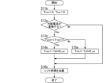
- FIG. 6 is a flowchart for explaining the operation of the control device in the power conversion device of the same.
- FIG. 7 is a flowchart for explaining the operation of the control device in the power conversion device of the same.
- FIG. 8 is a flowchart for explaining the operation of the control device in the power conversion device of the same.
- FIG. 9 is a timing chart for explaining the operation of the power conversion device, and is a timing chart in a period corresponding to region A2 in FIG.
- FIG. 10 is a flowchart for explaining the operation of the control device in the power conversion device of the same.
- FIG. 11 is a flowchart for explaining the operation of the control device in the power conversion device of the same.
- FIG. 12 is a flow chart for explaining the operation of the control device in the power conversion device of the same.
- 13 is a timing chart for explaining the operation of the power converter according to Modification 1 of Embodiment 1.
- FIG. 14 is a timing chart for explaining the operation of the same power converter.
- FIG. 15 is an explanatory diagram of the operation of the power converter same as above.
- FIG. 16 is an explanatory diagram of the operation of the power converter same as above.
- 17 is a timing chart for explaining the operation of the power converter according to Modification 2 of Embodiment 1.
- FIG. 18 is a timing chart for explaining the operation of the same power converter.
- 19 is a timing chart for explaining the operation of the power converter according to Modification 3 of Embodiment 1.
- FIG. FIG. 20 is a timing chart for explaining the operation of the same power converter.
- 21 is a circuit diagram of a power converter according to Embodiment 2.
- FIG. 22 is a circuit diagram showing another configuration example of the switch in the power converter according to the second embodiment
- FIG. 23 is a circuit diagram showing another configuration example of the switch in the power converter according to the second embodiment
- 24 is a circuit diagram of a power converter according to Embodiment 3.
- FIG. 25 is a circuit diagram of a power converter according to Embodiment 4.
- the power converter device 100 includes, for example, a first DC terminal 31 and a second DC terminal 32, a plurality of (for example, three) AC terminals 41, as shown in FIG. , a DC power source E1 is connected between the first DC terminal 31 and the second DC terminal 32, and an AC load RA1 is connected to the plurality of AC terminals 41.
- AC load RA1 is, for example, a three-phase motor.
- the power converter 100 converts the DC output from the DC power supply E1 into AC power and outputs the AC power to the AC load RA1.
- DC power source E1 includes, for example, a solar cell or a fuel cell.
- the DC power supply E1 may include a DC-DC converter.
- the power conversion device 100 connects the plurality of AC terminals 41 to the power system instead of the AC load RA1.
- the power converter 100 can convert the DC power from the DC power supply E1 into AC power and output it to the power system, and can also convert the AC power from the power system into DC power and output it to the DC power supply E1.
- a “power system” means an entire system for an electric power company such as an electric power company to supply electric power to power receiving facilities of consumers.
- the AC power is, for example, three-phase AC power having a U-phase, a V-phase and a W-phase.
- the power conversion device 100 includes a power conversion circuit 11, a plurality (eg, three) of switches 8, a plurality (eg, three) of resonance capacitors 9, a resonance inductor L1, a capacitor C1, and a control device. 50 and
- the power conversion circuit 11 has a plurality of (eg, three) first switching elements 1 and a plurality of (eg, three) second switching elements 2 .
- a plurality of (for example, three) switching circuits 10 each having a plurality of first switching elements 1 and a plurality of second switching elements 2 connected in series in a one-to-one relationship are connected in parallel.
- a plurality of first switching elements 1 are connected to a first DC terminal 31 and a plurality of second switching elements 2 are connected to a second DC terminal 32 .
- Each of the multiple switches 8 is, for example, a bidirectional switch.
- the plurality of AC terminals 41 correspond to the plurality of switching circuits 10 on a one-to-one basis.
- Each of the AC terminals 41 is connected to the connection point 3 of the first switching element 1 and the second switching element 2 in the corresponding switching circuit 10 .
- the plurality of switches 8 correspond to the plurality of switching circuits 10 on a one-to-one basis.
- Each of the plurality of switches 8 has a first end connected to the connection point 3 of the first switching element 1 and the second switching element 2 in the corresponding switching circuit 10, and a second end commonly connected to the common connection point 25. ing.
- the plurality of resonance capacitors 9 correspond to the plurality of switches 8 on a one-to-one basis. Each of the multiple resonance capacitors 9 is connected between the first end of the corresponding switch 8 and the second DC terminal 32 .
- the resonant inductor L1 has a first end and a second end, and the first end is connected to the common connection point 25 .
- a capacitor C1 is connected between the second end of the resonance inductor L1 and the second DC terminal 32 .
- the control device 50 controls the plurality of first switching elements 1 , the plurality of second switching elements 2 and the plurality of switches 8 .
- the control device 50 performs zero voltage soft switching on each of the plurality of first switching elements 1 and the plurality of second switching elements 2 .
- the power conversion device 100 includes the first DC terminal 31 and the second DC terminal 32, the power conversion circuit 11, and the plurality (for example, three) of the AC terminals 41. , a plurality (eg, three) of switches 8 , a plurality (eg, three) of resonance capacitors 9 , a resonance inductor L ⁇ b>1 , a capacitor C ⁇ b>1 , and a control device 50 .
- a plurality of (for example, three) switching circuits 10 each having a plurality of first switching elements 1 and a plurality of second switching elements 2 connected in series in a one-to-one relationship are connected in parallel.
- the power conversion device 100 also includes a protection circuit 17 .
- the power conversion device 100 further includes a capacitor C10.
- the capacitor C ⁇ b>10 is connected between the first DC terminal 31 and the second DC terminal 32 and connected in parallel with the power conversion circuit 11 .
- a DC power supply E1 is connected between the first DC terminal 31 and the second DC terminal 32, and AC loads RA1 are connected to a plurality of AC terminals 41.
- the switching circuits 10 corresponding to the U phase, V phase and W phase may be referred to as switching circuit 10U, switching circuit 10V and switching circuit 10W, respectively.
- the 1st switching element 1 and the 2nd switching element 2 of 10 U of switching circuits may be called the 1st switching element 1U and the 2nd switching element 2U.
- the first switching element 1 and the second switching element 2 of the switching circuit 10V may be referred to as the first switching element 1V and the second switching element 2V.
- connection point 3 between the first switching element 1U and the second switching element 2U is referred to as a connection point 3U
- the connection point 3 between the first switching element 1V and the second switching element 2V is referred to as a connection point 3V
- connection point 3V is referred to as a connection point 3V
- the connection point 3 between the one switching element 1W and the second switching element 2W may be referred to as a connection point 3W.
- the AC terminal 41 connected to the connection point 3U is referred to as an AC terminal 41U
- the AC terminal 41 connected to the connection point 3V is referred to as an AC terminal 41V
- the AC terminal 41 connected to the connection point 3W is referred to as an AC terminal 41V.
- Terminal 41 may also be referred to as AC terminal 41W.
- the resonance capacitor 9 connected in parallel to the second switching element 2U is referred to as a resonance capacitor 9U
- the resonance capacitor 9 connected in parallel to the second switching element 2V is referred to as a resonance capacitor 9V
- the resonance capacitor 9 connected in parallel to the second switching element 2W may be referred to as a resonance capacitor 9W.
- switch 8U the switch 8 connected to the connection point 3U
- switch 8V the switch 8 connected to the connection point 3V
- switch 8W the switch 8 connected to the connection point 3W. It is also called
- the first DC terminal 31 is connected to the high potential side output terminal (positive electrode) of the DC power source E1
- the second DC terminal 32 is connected to the low potential side output terminal (negative electrode) of the DC power source E1.
- the U-phase, V-phase and W-phase of the AC load RA1 are connected to three AC terminals 41U, 41V and 41W, respectively.
- each of the plurality of first switching elements 1 and the plurality of second switching elements 2 has a control terminal, a first main terminal and a second main terminal. Control terminals of the plurality of first switching elements 1 and the plurality of second switching elements 2 are connected to the control device 50 .
- the first main terminal of the first switching element 1 is connected to the first DC terminal 31, and the second main terminal of the first switching element 1 is connected to the second switching element 2.
- the second main terminal of the second switching element 2 is connected to the second DC terminal 32 .
- the first switching element 1 is a high side switching element (P side switching element) and the second switching element 2 is a low side switching element (N side switching element).
- Each of the plurality of first switching elements 1 and the plurality of second switching elements 2 is, for example, an IGBT (Insulated Gate Bipolar Transistor). Therefore, the control terminal, the first main terminal and the second main terminal of each of the plurality of first switching elements 1 and the plurality of second switching elements 2 are the gate terminal, the collector terminal and the emitter terminal, respectively.
- the power conversion circuit 11 includes a plurality of first diodes 4 connected in anti-parallel to the first switching elements 1 one-to-one, and a plurality of diodes 4 connected in anti-parallel to the second switching elements 2 one-to-one. and a second diode 5 .
- the anode of the first diode 4 is connected to the second main terminal (emitter terminal) of the first switching element 1 corresponding to this first diode 4
- the cathode of the first diode 4 is connected to the first main terminal (collector terminal) of the first switching element 1 corresponding to the first diode 4 .
- the anode of the second diode 5 is connected to the second main terminal (emitter terminal) of the second switching element 2 corresponding to this second diode 5, and the cathode of the second diode 5 is connected to the first main terminal (collector terminal) of the second switching element 2 corresponding to the second diode 5 .
- the U-phase of the AC load RA1 is connected to the connection point 3U between the first switching element 1U and the second switching element 2U via the AC terminal 41U.
- the V-phase of the AC load RA1 is connected to the connection point 3V between the first switching element 1V and the second switching element 2V through the AC terminal 41V.
- a connection point 3W between the first switching element 1W and the second switching element 2W is connected to, for example, the W phase of an AC load RA1 via an AC terminal 41W.
- the multiple first switching elements 1 and the multiple second switching elements 2 are controlled by the control device 50 .
- a plurality of resonance capacitors 9 correspond to a plurality of switches 8 on a one-to-one basis. Each of the multiple resonance capacitors 9 is connected between the first end of the corresponding switch 8 and the second DC terminal 32 .
- the power converter 100 has a plurality of resonant circuits.
- the plurality of resonance circuits include a resonance circuit having a resonance capacitor 9U and a resonance inductor L1, a resonance circuit having a resonance capacitor 9V and a resonance inductor L1, and a resonance capacitor 9W and a resonance inductor L1. and a resonant circuit.
- a plurality of resonance circuits share a resonance inductor L1.
- Each of the plurality of switches 8 has, for example, two first IGBTs 6 and second IGBTs 7 connected in anti-parallel.
- the collector terminal of the first IGBT 6 and the emitter terminal of the second IGBT 7 are connected, and the emitter terminal of the first IGBT 6 and the collector terminal of the second IGBT 7 are connected.
- the first IGBT 6 is connected to the node 3 of the switching circuit 10 corresponding to the switch 8 with that first IGBT 6 .
- the second IGBT 7 is connected to the node 3 of the switching circuit 10 corresponding to the switch 8 having that second IGBT 7.
- the switch 8U is connected to a connection point 3U between the first switching element 1U and the second switching element 2U.
- the switch 8V is connected to the connection point 3V between the first switching element 1V and the second switching element 2V.
- the switch 8W is connected to the connection point 3W between the first switching element 1W and the second switching element 2W.
- the first IGBT 6 and the second IGBT 7 of the switch 8U will be called the first IGBT 6U and the second IGBT 7U, respectively
- the first IGBT 6 and the second IGBT 7 of the switch 8V will be called the first IGBT 6V and the second IGBT 7V, respectively
- the switch 8W will be called the first IGBT 6V and the second IGBT 7V.
- the first IGBT 6 and the second IGBT 7 may also be referred to as the first IGBT 6W and the second IGBT 7W, respectively.
- the plurality of switches 8 are controlled by a control device 50.
- the first IGBT 6U, the second IGBT 7U, the first IGBT 6V, the second IGBT 7V, the first IGBT 6W and the second IGBT 7W are controlled by the control device 50.
- the resonance inductor L1 has a first end and a second end. A first end of the resonance inductor L1 is connected to the common connection point 25 . A second end of the resonant inductor L1 is connected to the capacitor C1.
- Capacitor C1 is connected between the second end of the resonance inductor L1 and the second DC terminal 32 .
- Capacitor C1 is, for example, a film capacitor.
- the protection circuit 17 has a third diode 13 and a fourth diode 14 .
- a third diode 13 is connected between the common connection point 25 and the first DC terminal 31 .
- the anode of the third diode 13 is connected to the common connection point 25 .
- the cathode of the third diode 13 is connected to the first DC terminal 31 .
- a fourth diode 14 is connected between the common connection point 25 and the second DC terminal 32 .
- the anode of the fourth diode 14 is connected to the second DC terminal 32 .
- the cathode of the fourth diode 14 is connected to the common connection point 25 . Therefore, the fourth diode 14 is connected in series with the third diode 13 .
- Capacitor C10 is connected between the first DC terminal 31 and the second DC terminal 32 and connected in parallel to the power conversion circuit 11 .
- Capacitor C10 is, for example, an electrolytic capacitor.
- the control device 50 controls the plurality of first switching elements 1 , the plurality of second switching elements 2 and the plurality of switches 8 .
- the execution subject of the control device 50 includes a computer system.
- a computer system has one or more computers.
- a computer system is mainly composed of a processor and a memory as hardware.
- the processor executes the program recorded in the memory of the computer system, thereby implementing the function of the control device 50 in the present disclosure as an execution entity.
- the program may be recorded in advance in the memory of the computer system, may be provided through an electric communication line, or may be stored in a non-temporary storage medium such as a computer system-readable memory card, optical disk, or hard disk drive (magnetic disk). may be recorded on a physical recording medium and provided.
- a processor in a computer system consists of one or more electronic circuits including semiconductor integrated circuits (ICs) or large scale integrated circuits (LSIs).
- ICs semiconductor integrated circuits
- LSIs large scale integrated circuits
- a plurality of electronic circuits may be integrated into one chip, or may be distributed over a plurality of chips.
- a plurality of chips may be integrated in one device, or may be distributed in a plurality of devices.
- the control device 50 outputs PWM (Pulse Width Modulation) signals SU1, SV1, and SW1 for controlling the on/off of the plurality of first switching elements 1U, 1V, and 1W, respectively.
- PWM Pulse Width Modulation
- Each of the PWM signals SU1, SV1, and SW1 has, for example, a first potential level (hereinafter also referred to as a low level) and a second potential level higher than the first potential level (hereinafter also referred to as a high level). ) and .
- the first switching elements 1U, 1V and 1W are respectively turned on when the PWM signals SU1, SV1 and SW1 are at high level, and turned off when they are at low level.
- the control device 50 also outputs PWM signals SU2, SV2 and SW2 for controlling the on/off of the plurality of second switching elements 2U, 2V and 2W, respectively.
- Each of the PWM signals SU2, SV2, and SW2 is a signal whose potential level changes between, for example, a first potential level and a second potential level higher than the first potential level.
- the second switching elements 2U, 2V and 2W are respectively turned on when the PWM signals SU2, SV2 and SW2 are at high level, and turned off when they are at low level.
- the control device 50 generates PWM signals SU1, SV1, and SW1 corresponding to the plurality of first switching elements 1U, 1V, and 1W, respectively, and the plurality of second switching elements using a sawtooth-shaped carrier signal (see FIG. 2).
- PWM signals SU2, SV2 and SW2 corresponding to 2U, 2V and 2W are generated. More specifically, control device 50 generates PWM signals SU1 and SU2 to be supplied to first switching element 1U and second switching element 2U, respectively, based on at least the carrier signal and the U-phase voltage command.
- control device 50 generates PWM signals SV1 and SV2 to be supplied to the first switching element 1V and the second switching element 2V, respectively, based on at least the carrier signal and the V-phase voltage command. Further, the control device 50 generates PWM signals SW1 and SW2 to be supplied to the first switching element 1W and the second switching element 2W, respectively, based on at least the carrier signal and the W-phase voltage command.
- the U-phase voltage command, the V-phase voltage command, and the W-phase voltage command are, for example, sinusoidal signals that are out of phase with each other by 120°, and their amplitudes (voltage command values) change with time.
- the U-phase voltage command, the V-phase voltage command, and the W-phase voltage command have the same length of one cycle. Also, the length of one cycle of the U-phase voltage command, the V-phase voltage command, and the W-phase voltage command is longer than the length of one cycle of the carrier signal.
- Control device 50 compares the U-phase voltage command and the carrier signal to generate PWM signal SU1 to be supplied to first switching element 1U.
- Control device 50 also inverts PWM signal SU1 applied to first switching element 1U to generate PWM signal SU2 applied to second switching element 2U.
- the controller 50 controls the period between the high level period of the PWM signal SU1 and the high level period of the PWM signal SU2 so that the ON periods of the first switching element 1U and the second switching element 2U do not overlap. is set to the dead time Td (see FIG. 2).
- Control device 50 compares the V-phase voltage command and the carrier signal to generate PWM signal SV1 to be supplied to first switching element 1V. Further, the control device 50 inverts the PWM signal SV1 to be applied to the first switching element 1V to generate the PWM signal SV2 to be applied to the second switching element 2V.
- the controller 50 controls the period between the high level period of the PWM signal SV1 and the high level period of the PWM signal SV2 so that the ON periods of the first switching element 1V and the second switching element 2V do not overlap. is set to the dead time Td (see FIG. 2).
- Control device 50 compares the W-phase voltage command and the carrier signal to generate PWM signal SW1 to be supplied to first switching element 1W. Further, the control device 50 inverts the PWM signal SW1 to be applied to the first switching element 1W to generate the PWM signal SW2 to be applied to the second switching element 2W.
- the controller 50 controls the period between the high level period of the PWM signal SW1 and the high level period of the PWM signal SW2 so that the ON periods of the first switching element 1W and the second switching element 2W do not overlap. is set to the dead time Td (see FIG. 3).
- the U-phase voltage command, the V-phase voltage command, and the W-phase voltage command are, for example, sinusoidal signals whose phases are different from each other by 120°, and their amplitudes change with time. Therefore, the duty of the PWM signal SU1, the duty of the PWM signal SV1, and the duty of the PWM signal SW1 change sinusoidally with a phase difference of 120°, for example, as shown in FIG. Similarly, the duty of the PWM signal SU2, the duty of the PWM signal SV2, and the duty of the PWM signal SW2 change sinusoidally with phases different from each other by 120°.
- the control device 50 generates PWM signals SU1, SU2, SV1, SV2, SW1, and SW2 based on the carrier signal, each voltage command, and information on the state of the AC load RA1.
- the information about the state of the AC load RA1 is, for example, detected values from a plurality of current sensors that detect currents flowing through the U-phase, V-phase, and W-phase of the AC load RA1. including.
- the plurality of switches 8, the resonance inductor L1, the plurality of resonance capacitors 9 and C1, and the protection circuit 17 are provided to perform zero voltage soft switching of the plurality of first switching elements 1 and the plurality of second switching elements 2. It is
- control device 50 also controls the plurality of switches 8 in addition to the plurality of first switching elements 1 and second switching elements 2 of the power conversion circuit 11 .
- the control device 50 generates control signals SU6, SU7, SV6, SV7, SW6, and SW7 for controlling on/off of the first IGBT 6U, the second IGBT 7U, the first IGBT 6V, the second IGBT 7V, the first IGBT 6W, and the second IGBT 7W. Output to the gate terminals of the 2IGBT 7U, the 1st IGBT 6V, the 2nd IGBT 7V, the 1st IGBT 6W and the 2nd IGBT 7W.
- the switch 8U charges the resonance capacitor 9U by flowing through the path of the capacitor C1-resonance inductor L1-switch 8U-resonance capacitor 9U. pass through.
- the switch 8U discharges the charge of the resonance capacitor 9U through the path of the resonance capacitor 9U, the switch 8U, the resonance inductor L1, and the capacitor C1. Pass the discharge current.
- the switch 8V when the first IGBT 6V is on and the second IGBT 7V is off, the charging current flows through the path of the capacitor C1-resonance inductor L1-switch 8V-resonance capacitor 9V to charge the resonance capacitor 9V. pass through.
- the switch 8V discharges the charge of the resonance capacitor 9V through the path of the resonance capacitor 9V, the switch 8V, the resonance inductor L1, and the capacitor C1. Pass the discharge current.
- the switch 8W when the first IGBT 6W is on and the second IGBT 7W is off, the charging current flows through the path of the capacitor C1-resonance inductor L1-switch 8W-resonance capacitor 9W to charge the resonance capacitor 9W. pass through.
- the switch 8W discharges the charge of the resonance capacitor 9W through the path of the resonance capacitor 9W, the switch 8W, the resonance inductor L1, and the capacitor C1. Pass the discharge current.
- the current flowing through the resonant inductor L1 is iL1
- the current flowing through the U phase of the AC load RA1 is iU
- the current flowing through the V phase of the AC load RA1 is iV
- the AC load A current flowing through the W phase of RA1 is assumed to be iW.
- the polarities of the currents iL1, iU, iV, and iW flowing in the directions of the arrows in FIG. 1 are assumed to be positive, and the directions of the arrows in FIG. The polarity of the time is explained as negative.
- the power conversion device 100 includes the protection circuit 17 having the third diode 13 and the fourth diode 14 as described above.
- the protection circuit 17 having the third diode 13 and the fourth diode 14 as described above.
- the power conversion device 100 for example, when the second IGBT 7U of the switch 8U is turned on and a negative current iL1 is flowing through the resonance inductor L1, when the second IGBT 7U is turned off, the energy of the resonance inductor L1 is Current flows through the path of the fourth diode 14-resonant inductor L1-capacitor C1 until the consumed current iL1 flowing through the resonant inductor L1 becomes zero.
- the resonance inductor L1 is consumed and the current iL1 flowing through the resonance inductor L1 is regenerated to the power conversion circuit 11 via the third diode 13 until the current iL1 flowing through the resonance inductor L1 becomes zero.
- the power conversion device 100 for example, when the second IGBT 7V of the switch 8V is turned on and a negative current iL1 is flowing through the resonance inductor L1, when the second IGBT 7V is turned off, the energy of the resonance inductor L1 is Current flows through the path of the fourth diode 14-resonant inductor L1-capacitor C1 until the consumed current iL1 flowing through the resonant inductor L1 becomes zero.
- the resonance inductor L1 is consumed and the current iL1 flowing through the resonance inductor L1 is regenerated to the power conversion circuit 11 via the third diode 13 until the current iL1 flowing through the resonance inductor L1 becomes zero.
- the power conversion device 100 for example, when the second IGBT 7W of the switch 8W is turned on and a negative current iL1 is flowing through the resonance inductor L1, when the second IGBT 7W is turned off, the energy of the resonance inductor L1 is Current flows through the path of the fourth diode 14-resonant inductor L1-capacitor C1 until the consumed current iL1 flowing through the resonant inductor L1 becomes zero.
- the control device 50 turns on the first IGBT 6 corresponding to the first switching element 1 to be subjected to zero-voltage soft switching control to turn on the resonance inductor L1 and the resonance inductor L1 connected in series to the first switching element 1.
- the voltage across the first switching element 1 becomes zero.
- the control device 50 turns on the second IGBT 7 corresponding to the second switching element 2 to be subjected to zero voltage soft switching control to turn on the resonance inductor L1 and the resonance inductor L1 connected in parallel to the second switching element 2.
- the control device 50 charges and discharges the resonance capacitor 9 through the switch 8 so that the dead time Td and the half cycle ( ⁇ LC) of the LC resonance are matched. Thereby, the power conversion device 100 can realize zero voltage soft switching.
- FIG. 2 shows PWM signals SU1 and SU2 given from the control device 50 to the first switching element 1U and the second switching element 2U of the switching circuit 10U, respectively.
- FIG. 2 also shows a control signal SU6 supplied from the control device 50 to the first IGBT 6U of the switch 8U, a current iU flowing through the U phase of the AC load RA1, a current iL1 flowing through the resonance inductor L1, and the first switching element 1U. and the voltage V 1U across the .
- FIG. 2 also shows PWM signals SV1 and SV2 supplied from the control device 50 to the first switching element 1V and the second switching element 2V of the switching circuit 10V, respectively.
- FIG. 2 also shows a control signal SV6 given from the control device 50 to the first IGBT 6V of the switch 8V, a current iV flowing through the V phase of the AC load RA1, a current iL1 flowing through the resonance inductor L1, and the first switching element 1V. and the voltage V 1 V across the .
- FIG. 2 also shows the dead time Td set in the control device 50 to prevent the first switching element 1 and the second switching element 2 of the same phase from being turned on at the same time. 2 also shows an additional time Tau set for the control signal SU6 of the first IGBT 6U of the switch 8U in the control device 50 and an additional time Tav set for the control signal SV6 of the first IGBT 6V of the switch 8V. Illustrated.
- FIG. 3 shows PWM signals SW1 and SW2 supplied from the control device 50 to the first switching element 1W and the second switching element 2W of the switching circuit 10W, respectively.
- FIG. 3 shows the control signal SW6 given from the control device 50 to the first IGBT 6W of the switch 8W and the current iW flowing through the W phase of the AC load RA1.
- FIG. 3 also shows the current iL1 flowing through the resonance inductor L1.
- FIG. 3 also shows the voltage V1W across the first switching element 1W.
- FIG. 3 also shows the dead time Td set in the control device 50 to prevent the first switching element 1W and the second switching element 2W from being turned on at the same time.
- FIG. 3 also shows the additional time Taw set for the control signal SW6 of the first IGBT 6W of the switch 8W in the control device 50. As shown in FIG.
- the control device 50 sets the control signal SU6 applied to the first IGBT 6U of the switch 8U to the high level period starting time t1 as a dead time for preventing the first switching element 1U and the second switching element 2U from being turned on at the same time. This is the time set to make the high level period of the control signal SU6 longer than the dead time Td earlier than the start time t2 of the time Td.
- the length of the additional time Tau is set based on the value of the current iU. In order to start the LC resonance from the start time t2 of the dead time Td, it is desirable that the value of the current iL1 matches the value of the current iU at the start time t2 of the dead time Td.
- the end point of the high level period of the control signal SU6 may be the same as or later than the end point t3 of the dead time Td.
- FIG. 2 shows an example in which the end point of the high level period of the control signal SU6 is set to be the same as the end point t3 of the dead time Td.
- the control device 50 sets the high level period of the control signal SU6 to Tau+Td.
- the voltage V1U across the first switching element 1U becomes zero at the end time t3 of the dead time Td.
- the current iL1 flowing through the resonance inductor L1 starts flowing at the start time t1 of the high level period of the control signal SU6, and becomes zero at the time t4 after the additional time Tau has passed from the end time t3 of the dead time Td. become.
- the current iL1 at this time since iL1 ⁇ iU from the start time t2 of the dead time Td, the current iL1 in the shaded region of the current waveform in the fifth row from the top in FIG. 2 flows into the resonance capacitor 9U. LC resonance occurs.
- the current iL1 is regenerated to the power conversion circuit 11 via the third diode 13 after the dead time Td ends at t3.
- the high level period of the control signal SV6 applied to the first IGBT 6V of the switch 8V in the control device 50 is advanced earlier than the start time t6 of the dead time Td.
- the length of the additional time Tav is set based on the value of the current iV. In order to start the LC resonance from the start time t6 of the dead time Td, it is desirable that the value of the current iL1 matches the value of the current iV at the start time t6 of the dead time Td.
- the end point of the high level period of the control signal SV6 may be the same as or later than the end point t7 of the dead time Td.
- FIG. 2 shows an example in which the end point of the high level period of the control signal SV6 is set to be the same as the end point t7 of the dead time Td.
- the control device 50 sets the high level period of the control signal SV6 to Tav+Td.
- the voltage V1V across the first switching element 1V becomes zero at the end time t7 of the dead time Td.
- the current iL1 flowing through the resonance inductor L1 starts flowing at time t5 when the high level period of the control signal SV6 starts, and becomes zero at time t8 after the additional time Tav has passed from time t7 when the dead time Td ends. become.
- the current iL1 at this time since iL1 ⁇ iV from the start point t6 of the dead time Td, the current iL1 in the shaded region of the current waveform in the tenth row from the top in FIG. 2 flows into the resonance capacitor 9V. LC resonance occurs.
- the current iL1 is regenerated to the power conversion circuit 11 via the third diode 13 after the dead time Td ends at t7.
- the high level period of the control signal SW6 applied to the first IGBT 6W of the switch 8W in the control device 50 is advanced earlier than the start time t10 of the dead time Td.
- the additional time Taw is set based on the value of the current iW. In order to start the LC resonance from the start time t10 of the dead time Td, it is desirable that the value of the current iL1 matches the value of the current iW at the start time t10 of the dead time Td.
- the end point of the high level period of the control signal SW6 may be the same as or later than the end point t11 of the dead time Td.
- FIG. 3 shows an example in which the end point of the high level period of the control signal SW6 is set to be the same as the end point t11 of the dead time Td.
- the control device 50 sets the high level period of the control signal SW6 to Taw+Td.
- the voltage V1W across the first switching element 1W becomes zero at the end time t11 of the dead time Td.
- the current iL1 flowing through the resonance inductor L1 starts flowing at time t9 when the high level period of the control signal SW6 starts, and becomes zero at time t12 after the additional time Taw has passed from the end time t11 of the dead time Td. become.
- the current iL1 at this time since iL1 ⁇ iW from the start time t10 of the dead time Td, the current iL1 in the shaded region of the current waveform in the fourth row from the top in FIG. 3 flows into the resonance capacitor 9W. LC resonance occurs.
- the current iL1 is regenerated to the power conversion circuit 11 via the third diode 13 after the dead time Td ends at t11.
- the control device 50 sets the dead time Td to start LC resonance at the start time t2 of the dead time Td between the high level period of the PWM signal SU1 and the high level period of the PWM signal SU2.
- the detection value at the carrier cycle to which the additional time Tau is added, or at the timing closest to the carrier cycle, or the like is used.
- the estimated value of the current iU at this time a value or the like obtained by estimating the current iU in the carrier cycle to which the additional time Tau is added is used.
- the control device 50 sets the dead time Td to start LC resonance at the starting point t6 of the dead time Td between the high level period of the PWM signal SV1 and the high level period of the PWM signal SV2.
- the detection value at the carrier cycle to which the additional time Tav is added, or at the timing closest to the carrier cycle, or the like is used.
- the estimated value of the current iV at this time a value obtained by estimating the current iV in the carrier cycle to which the additional time Tav is added, or the like is used.
- the phases of the three-phase (U-phase, V-phase, and W-phase) voltage commands are different from each other by 120°, but the command values of the two-phase voltage commands approach each electrical angle of 60°,
- the duties of the two-phase PWM signals approach each other (see area A1 and area A2 in FIG. 4).
- the duty of the U-phase PWM signal and the V-phase PWM signal is around 0.75.
- the duty of the U-phase PWM signal and the V-phase PWM signal is around 0.25.
- the resonant current becomes a positive current iL1.
- the resonance current becomes a negative current iL1.
- the time t1 of the high level period of the control signal SU6 applied to the first IGBT 6U and the start time t5 of the high level period of the control signal SV6 applied to the first IGBT 6V. is shortened, and there is a possibility that the U-phase resonance current and the V-phase resonance current flow through the resonance inductor L1 at the same time.
- the direction of the resonance current is opposite to that in region A1. be.
- the control device 50 determines that two-phase resonance currents corresponding to two switching circuits 10 out of the plurality of switching circuits 10 flow through the resonance inductor L1 at the same time, two Control is performed to shift the ON period of each of the first switching element 1 and the second switching element 2 in one switching circuit 10 out of the two switching circuits 10 .
- two Control is performed to shift the ON period of each of the first switching element 1 and the second switching element 2 in one switching circuit 10 out of the two switching circuits 10 .
- FIG. 2 is a diagram showing an example of boundary conditions when the U-phase resonance current and the V-phase resonance current do not overlap (do not flow simultaneously) and overlap (flow simultaneously).
- the boundary conditions will be described with reference to FIG.
- the power converter 100 starts the high level period of the PWM signal SU1 given to the first switching element 1U of the switching circuit 10U and the start time t3 of the high level period of the PWM signal SV1 given to the first switching element 1V of the switching circuit 10V.
- a threshold for the time difference is set to, for example, (Tau+Tav+Td). It can be estimated that the resonance currents corresponding to the two phases of and flow simultaneously.
- the setting of the above threshold value is an example, and setting other values is also conceivable.
- the method of calculating the time difference used to determine whether two-phase resonance currents flow simultaneously is not limited to the above example, and other calculation methods may be used as long as the time difference corresponding to the time difference can be calculated.
- the end point t2 of the high level period of the PWM signal SU2 applied to the second switching element 2U of the switching circuit 10U and the switching circuit 10V A time difference from the end point t6 of the high level period of the PWM signal SV2 given to the second switching element 2V may be used.
- the time difference is less than (Tau+Tav+Td) and the resonance currents overlap
- the time at which the resonance currents of the two phases actually overlap is Tov_uv.
- the V-phase (or U-phase) resonance current begins to flow immediately after the U-phase (or V-phase) resonance current stops flowing.
- the power conversion device 100 includes the start time t3 of the high level period of the PWM signal SU1 given to the first switching element 1U of the switching circuit 10U and the high level period of the PWM signal SW1 given to the first switching element 1W of the switching circuit 10W. If the time difference from the start time t11 is (Tau+Taw+Td) or more, the resonance current of the U phase and the resonance current of the W phase do not overlap, and if the time difference is less than (Tau+Taw+Td), the resonance current of the U phase and It overlaps with the resonance current of the W phase. That is, from the above boundary conditions, a threshold for the time difference is set to, for example, (Tau+Taw+Td).
- the resonance currents corresponding to the two phases of and flow simultaneously can be estimated that the resonance currents corresponding to the two phases of and flow simultaneously.
- the setting of the above threshold value is an example, and setting other values is also conceivable.
- the above threshold may be set to a value that is even larger than (Tau+Taw+Td).
- the method of calculating the time difference used to determine whether two-phase resonance currents flow simultaneously is not limited to the above example, and other calculation methods may be used as long as the time difference corresponding to the time difference can be calculated.
- the end point t2 of the high level period of the PWM signal SU2 applied to the second switching element 2U of the switching circuit 10U and the time t2 of the switching circuit 10W A time difference from the end time t10 of the high level period of the PWM signal SW2 supplied to the second switching element 2W may be used.
- the time difference is less than (Tau+Taw+Td) and the resonance currents overlap, the time at which the resonance currents of the two phases actually overlap is Tov_uw.
- the power converter 100 has a start point t7 of the high level period of the PWM signal SV1 given to the first switching element 1V of the switching circuit 10V and a high level period of the PWM signal SW1 given to the first switching element 1W of the switching circuit 10W. If the time difference from the start time t11 is (Tav+Taw+Td) or more, the resonance current of the V phase and the resonance current of the W phase do not overlap, and if the time difference is less than (Tav+Taw+Td), the resonance current of the V phase and It overlaps with the resonance current of the W phase.
- a threshold value for the time difference is set to, for example, (Tav+Taw+Td). It can be estimated that the resonance currents corresponding to the two phases of and flow simultaneously.
- the setting of the above threshold value is an example, and setting other values is also conceivable. For example, in consideration of the error of the additional time Tav and the error of the additional time Taw, it is conceivable to set the above threshold value to a value even greater than (Tav+Taw+Td).
- the method of calculating the time difference used to determine whether two-phase resonance currents flow simultaneously is not limited to the above example, and other calculation methods may be used as long as the time difference corresponding to the time difference can be calculated.
- the end point t6 of the high level period of the PWM signal SV2 applied to the second switching element 2V of the switching circuit 10V and the switching circuit 10W A time difference from the end time t10 of the high level period of the PWM signal SW2 supplied to the second switching element 2W may be used.
- the time difference is less than (Tav+Taw+Td) and the resonance currents overlap, the time at which the resonance currents of the two phases actually overlap is Tov_vw.
- FIG. 5 shows an example of a timing chart in a period corresponding to area A1 in FIG.
- the PWM signals SU1, SU2, SV1, and SV2 before shifting and the control signals SU6, SU7, and A timing chart of SV6 and SV7 is shown.
- the PWM signals SU1, SU2, SV1, SV2, the control signals SU6, SU7, SV6, SV7, and the current iL1 when the PWM signal SU1 and the PWM signal SU2 are shifted by the same additional time Tau.
- a timing chart is shown.
- the power converter 100 can suppress overlap between the U-phase resonance current and the V-phase resonance current.
- Tvs be the shift time when shifting the ON period of each of the two switching elements 2V
- Tws be the shift time when shifting the ON period of each of the first switching element 1W and the second switching element 2W of the switching circuit 10W.
- control device 50 shifts the ON period of each of the PWM signal SU1 and PWM signal SU2, it does not change the duty of each of PWM signal SU1 and PWM signal SU2 in one cycle of the carrier signal. Further, when the control device 50 shifts the ON period of each of the PWM signal SV1 and the PWM signal SV2, it does not change the duty of each of the PWM signal SV1 and the PWM signal SV2 in one cycle of the carrier signal. Further, when the control device 50 shifts the ON period of each of the PWM signal SW1 and the PWM signal SW2, it does not change the duty of each of the PWM signal SW1 and the PWM signal SW2 in one cycle of the carrier signal.
- Tuon be the time width of the high level period of the PWM signal SU1 corresponding to the first switching element 1U
- Tvon be the time width of the high level period of the PWM signal SV1 corresponding to the first switching element 1V.
- Twon be the time width of the high level period of the PWM signal SW1 corresponding to 1W.
- the ON period of the first switching element 1U corresponds to the high level period of the PWM signal SU1 on a one-to-one basis.
- the ON period of the first switching element 1V corresponds to the high level period of the PWM signal SV1 on a one-to-one basis.
- the ON period of the first switching element 1W corresponds to the high level period of the PWM signal SW1 on a one-to-one basis.
- control device 50 generates the PWM signal SU1, the PWM signal SV1, and the PWM signal SW1 for each period of the carrier signal, and then suppresses superimposition of the U-phase resonance current and the V-phase resonance current. a second process for suppressing superimposition of the U-phase resonance current and the W-phase resonance current; and a third process for suppressing the superimposition of the V-phase resonance current and the W-phase resonance current. ,I do.
- control device 50 determines whether or not the U-phase resonance current corresponding to switching circuit 10U and the V-phase resonance current corresponding to switching circuit 10V simultaneously flow (overlap) in resonance inductor L1. It judges (step S12).
- step S12 determines whether Tuon ⁇ Tvon (step S13).
- the control device 50 shifts each timing at which the signal level of the PWM signal SU1 changes by the predetermined period Tshift_uv in the direction of delay. That is, the control device 50 shifts the ON period of the first switching element 1U in a predetermined direction (the direction of delaying on the time axis).
- step S12 determines that the U-phase resonance current and the V-phase resonance current do not overlap (step S12: No)
- the control device 50 controls the first switching element 1U and the first switching element 1V by the PWM signal SU1 and the PWM signal SV1 after step S16, respectively.
- Tshift_uv is a predetermined period.
- Tshift_uv is set to Tov_uv, the time during which the two-phase resonance currents of the U phase and the V phase actually overlap. Duplication can be suppressed.
- step S21 the controller 50 determines whether or not the U-phase resonance current corresponding to the switching circuit 10U and the W-phase resonance current corresponding to the switching circuit 10W simultaneously flow through the resonance inductor L1 (step S22).
- step S22 determines whether Tuon ⁇ Twon (step S23).
- the control device 50 shifts each timing at which the signal level of the PWM signal SU1 changes by the predetermined period Tshift_uw in the direction of delay on the time axis. That is, the control device 50 shifts the ON period of the first switching element 1U in a predetermined direction (the direction of delaying on the time axis).
- the control device 50 controls the first switching element 1U and the first switching element 1W with the PWM signal SU1 and the PWM signal SW1 after step S26, respectively.
- Tshift_uw is a predetermined period.
- Tshift_uw is set to Tov_uw, the time during which the two-phase resonance currents of the U phase and the W phase actually overlap. Duplication can be suppressed.
- step S31 the controller 50 determines whether or not the V-phase resonance current corresponding to the switching circuit 10V and the W-phase resonance current corresponding to the switching circuit 10W simultaneously flow through the resonance inductor L1 (step S32).
- control device 50 determines whether Tvon ⁇ Twon (step S33).
- the control device 50 shifts each timing at which the signal level of the PWM signal SV1 changes by a predetermined period Tshift_vw in the direction of delay on the time axis. That is, the control device 50 shifts the ON period of the first switching element 1V in a predetermined direction (the direction of delaying on the time axis).
- the control device 50 controls the first switching element 1V and the first switching element 1W with the PWM signal SV1 and the PWM signal SW1 after step S36, respectively.
- the controller 50 determines that the V-phase resonance current and the W-phase resonance current overlap, the PWM signal SV1 or the PWM signal SW1 has a short high-level period. shift the signal.
- Tshift_vw is a predetermined period. In the power conversion device 100 according to the first embodiment, by setting Tshift_vw to the time Tov_vw during which the two-phase resonance currents of the V phase and the W phase actually overlap, the resonance current of the V phase and the resonance current of the W phase Duplication can be suppressed.
- FIG. 9 shows an example of a timing chart in a period corresponding to area A2 in FIG.
- the control device 50 determines that the two-phase resonance currents of the U-phase and the V-phase flow simultaneously, the PWM signals SU1, SU2, SV1, SV2 before shifting, the control signals SU6, SU7, Timing charts of SV6, SV7 and current iL1 are shown.
- the lower part of FIG. 9 shows that the two-phase resonance currents of the U-phase and the V-phase flow simultaneously.
- a timing chart is shown. As can be seen from the waveform of the current iL1 in FIG. 9, the power conversion device 100 can suppress overlap between the U-phase resonance current and the V-phase resonance current.
- control device 50 An example of the operation of the control device 50 during the period corresponding to the area A2 in FIG. 4 will be described below with reference to FIGS. The description of the operation of is omitted as appropriate.
- control device 50 generates the PWM signal SU1, the PWM signal SV1, and the PWM signal SW1 for each period of the carrier signal, and then suppresses superimposition of the U-phase resonance current and the V-phase resonance current. a second process for suppressing superimposition of the U-phase resonance current and the W-phase resonance current; and a third process for suppressing the superimposition of the V-phase resonance current and the W-phase resonance current. ,I do.
- step S11a the control device 50 determines whether or not the U-phase resonance current corresponding to the switching circuit 10U and the V-phase resonance current corresponding to the switching circuit 10V simultaneously flow (overlap) in the resonance inductor L1. It judges (step S12a).
- step S12a determines whether Tuon ⁇ Tvon (step S13a).
- the control device 50 controls the first switching element 1U and the first switching element 1V by the PWM signal SU1 and the PWM signal SV1 after step S16a, respectively.
- Tshift_uv is a predetermined period.
- Tshift_uv is set to Tov_uv, the time during which the two-phase resonance currents of the U phase and the V phase actually overlap. Duplication can be suppressed.
- step S21a the controller 50 determines whether or not the U-phase resonance current corresponding to the switching circuit 10U and the W-phase resonance current corresponding to the switching circuit 10W simultaneously flow through the resonance inductor L1 (step S22a).
- step S22a determines whether Tuon ⁇ Twon (step S23a).
- the control device 50 shifts each timing at which the signal level of the PWM signal SU1 changes by ⁇ Tshift_uw in the direction of delay on the time axis (in other words, shifts it by Tshift_uw in the direction of advance on the time axis). In other words, the control device 50 shifts the ON period of the first switching element 1U in a predetermined direction (advance on the time axis).
- the control device 50 controls the first switching element 1U and the first switching element 1W by the PWM signal SU1 and the PWM signal SW1 after step S26a, respectively.
- Tshift_uw is a predetermined period.
- Tshift_uw is set to Tov_uw, the time during which the two-phase resonance currents of the U phase and the W phase actually overlap. Duplication can be suppressed.
- step S31a the controller 50 determines whether or not the V-phase resonance current corresponding to the switching circuit 10V and the W-phase resonance current corresponding to the switching circuit 10W simultaneously flow through the resonance inductor L1 (step S32a).
- control device 50 determines whether or not Tvon ⁇ Twon (step S33a).
- the control device 50 shifts each timing at which the signal level of the PWM signal SV1 changes by ⁇ Tshift_vw in the direction of delay on the time axis (in other words, shifts it by Tshift_vw in the direction of advance on the time axis). That is, the control device 50 shifts the ON period of the first switching element 1V in a predetermined direction (advance on the time axis).
- the control device 50 controls the first switching element 1V and the first switching element 1W with the PWM signal SV1 and the PWM signal SW1 after step S36a, respectively.
- the controller 50 determines that the V-phase resonance current and the W-phase resonance current overlap, the PWM signal SV1 or the PWM signal SW1 has a short high-level period. shift the signal.
- Tshift_vw is a predetermined period. In the power conversion device 100 according to the first embodiment, by setting Tshift_vw to the time Tov_vw during which the two-phase resonance currents of the V phase and the W phase actually overlap, the resonance current of the V phase and the resonance current of the W phase Duplication can be suppressed.
- the power conversion device 100 includes a first DC terminal 31 and a second DC terminal 32, a power conversion circuit 11, a plurality of AC terminals 41, a plurality of switches 8, a plurality of resonance a capacitor 9 for resonance, an inductor L1 for resonance, a capacitor C1, and a control device 50.
- the power conversion circuit 11 has a plurality of first switching elements 1 and a plurality of second switching elements 2 .
- a plurality of switching circuits 10 each having a plurality of first switching elements 1 and a plurality of second switching elements 2 connected in series in a one-to-one relationship are connected in parallel.
- a plurality of first switching elements 1 are connected to a first DC terminal 31 and a plurality of second switching elements 2 are connected to a second DC terminal 32 .
- the plurality of AC terminals 41 correspond to the plurality of switching circuits 10 on a one-to-one basis. Each of the AC terminals 41 is connected to the connection point 3 of the first switching element 1 and the second switching element 2 in the corresponding switching circuit 10 .
- the plurality of switches 8 correspond to the plurality of switching circuits 10 on a one-to-one basis. Each of the plurality of switches 8 has a first end connected to the connection point 3 of the first switching element 1 and the second switching element 2 in the corresponding switching circuit 10, and a second end connected to the common connection point 25.
- the plurality of resonance capacitors 9 correspond to the plurality of switches 8 on a one-to-one basis. Each of the multiple resonance capacitors 9 is connected between the first end of the corresponding switch 8 and the second DC terminal 32 .
- the resonant inductor L1 has a first end and a second end. A first end of the resonance inductor L1 is connected to the common connection point 25 .
- a capacitor C1 is connected between the second end of the resonance inductor L1 and the second DC terminal 32 .
- the control device 50 controls the plurality of first switching elements 1 , the plurality of second switching elements 2 and the plurality of switches 8 .
- controller 50 determines that two-phase resonant currents corresponding to two switching circuits 10 out of a plurality of switching circuits 10 simultaneously flow through resonance inductor L1, one switching circuit 10 out of the two switching circuits 10 Control is performed to shift the ON period of each of the first switching element 1 and the second switching element 2 in .
- the power conversion device 100 can suppress simultaneous flow of two-phase resonance currents in the resonance inductor L1, and can more reliably perform soft switching. More specifically, the power conversion device 100 according to the first embodiment adopts a configuration in which a common resonance inductor L1 is connected to a plurality of switching circuits, but a two-phase resonance current is generated in the resonance inductor L1.
- the power conversion device 100 can suppress heat generation and loss due to an increase in the maximum value of the resonant current by suppressing simultaneous flow of two-phase resonant currents in the resonant inductor L1. becomes.
- Embodiment 1 also discloses the following control method.
- the control method is a control method for the power conversion device 100 .
- the power conversion device 100 includes a first DC terminal 31 and a second DC terminal 32, a power conversion circuit 11, a plurality of AC terminals 41, a plurality of switches 8, a plurality of resonance capacitors 9, and a resonance inductor L1. and a capacitor C1.
- the power conversion circuit 11 has a plurality of first switching elements 1 and a plurality of second switching elements 2 .
- a plurality of switching circuits 10 each having a plurality of first switching elements 1 and a plurality of second switching elements 2 connected in series in a one-to-one relationship are connected in parallel.
- a plurality of first switching elements 1 are connected to a first DC terminal 31 and a plurality of second switching elements 2 are connected to a second DC terminal 32 .
- the plurality of AC terminals 41 correspond to the plurality of switching circuits 10 on a one-to-one basis. Each of the AC terminals 41 is connected to the connection point 3 of the first switching element 1 and the second switching element 2 in the corresponding switching circuit 10 .
- the plurality of switches 8 correspond to the plurality of switching circuits 10 on a one-to-one basis. Each of the plurality of switches 8 has a first end connected to the connection point 3 of the first switching element 1 and the second switching element 2 in the corresponding switching circuit 10, and a second end connected to the common connection point 25.
- the resonant inductor L1 has a first end and a second end. A first end of the resonance inductor L1 is connected to the common connection point 25 .
- the plurality of resonance capacitors 9 correspond to the plurality of switches 8 on a one-to-one basis. Each of the multiple resonance capacitors 9 is connected between the first end of the corresponding switch 8 and the second DC terminal 32 .
- a capacitor C1 is connected between the second end of the resonance inductor L1 and the second DC terminal 32 .
- the control method includes a first step and a second step. In the first step, it is determined whether two-phase resonant currents corresponding to two switching circuits 10 out of the plurality of switching circuits 10 flow through the resonant inductor L1 at the same time.
- the first switching element 1 and the second switching element in one of the two switching circuits 10 are switched. 2 performs control to shift each ON period.
- this control method it is possible to suppress two-phase resonant currents from flowing through the resonant inductor L1 at the same time, so that soft switching (zero voltage soft switching) can be performed more reliably. Moreover, according to this control method, it is possible to suppress heat generation and loss due to an increase in the maximum value of the resonance current.
- Modification 1 of Embodiment 1 Since the circuit configuration of the power converter 100 according to Modification 1 of Embodiment 1 is the same as that of the power converter 100 (see FIG. 1) according to Embodiment 1, illustration of the circuit diagram is omitted. The operation of the power converter 100 according to Modification 1 of Embodiment 1 will be described below with reference to FIGS.
- the control device 50 connects two switching circuits 10 among the plurality of switching circuits 10 to the resonance inductor L1.
- control is performed to shift the ON period of each of the first switching element 1 and the second switching element 2 in one switching circuit 10 out of the two switching circuits 10.
- the control device 50 only advances each timing at which the signal level of the PWM signal changes on the time axis in the period corresponding to the region A1 in FIG. shift. That is, the control device 50 shifts the ON period of each of the first switching element 1 and the second switching element 2 in the one switching circuit 10 in a predetermined direction (a direction to advance on the time axis).
- the control device 50 determines that the two-phase resonance currents of the U-phase and the V-phase flow simultaneously, the PWM signals SU1, SU2, SV1, and SV2 before shifting and the control signal SU6 , SU7, SV6, SV7 and the timing chart of the current iL1.
- the PWM signals SU1, SU2, SV1, SV2, the control signals SU6, SU7, SV6, SV7, and the current iL1 when the PWM signal SU1 and the PWM signal SU2 are shifted by the same predetermined period Tshift_uv.
- Tshift_uv A timing chart is shown.
- Tshift_uv is set to a time obtained by adding a predetermined period to the time Tov_uv at which the two-phase resonance currents of the U phase and the V phase actually overlap. It is possible to suppress overlap between the resonance current and the V-phase resonance current.
- the control device 50 only delays each timing at which the signal level of the PWM signal changes on the time axis in the period corresponding to the region A2 in FIG. shift. That is, the control device 50 shifts the ON period of each of the first switching element 1 and the second switching element 2 in the one switching circuit 10 in a predetermined direction (the direction of delaying on the time axis).
- the control device 50 determines that the two-phase resonance currents of the U-phase and the V-phase flow simultaneously, the PWM signals SU1, SU2, SV1, and SV2 before shifting and the control signal SU6 , SU7, SV6, SV7 and the timing chart of the current iL1.
- the PWM signals SU1, SU2, SV1 and SV2 the control signals SU6, SU7, SV6 and SV7 and the current iL1 when the PWM signals SV1 and SV2 are shifted by the same predetermined period Tshift_uv.
- Tshift_uv A timing chart is shown.
- Tshift_uv is set to a time obtained by adding a predetermined period to the time Tov_uv at which the two-phase resonance currents of the U phase and the V phase actually overlap. It is possible to suppress overlap between the resonance current and the V-phase resonance current.
- the power conversion device 100 according to Modification 1 of Embodiment can suppress simultaneous flow of two-phase resonance currents in the resonance inductor L1. It is possible to reliably perform soft switching (zero voltage soft switching). Note that the operation of the power conversion device 100 according to Modification 1 of Embodiment 1 is illustrated only when it is determined that the two-phase resonance currents of the U phase and the V phase flow simultaneously, but the operation is limited to this. do not have. That is, the description of an example of the operation of the control device 50 when it is determined that two phases of resonance currents, ie, the U phase and the W phase, and the V phase and the W phase, flow simultaneously is omitted.
- the control device 50 includes the first switching element 1 and the second switching element 2 in the same manner as the control device 50 of the power conversion device 100 according to Embodiment 1.
- the first control mode and the second control mode may be executed alternately or at an arbitrary ratio.
- the line-to-line voltage (UV line-to-line voltage) between the U phase and the V phase changes as shown in FIG. 15 before and after the ON period of the first switching element 1U is shifted.
- the control device 50 executes the second control mode
- the phase-to-phase voltage between the U phase and the V phase changes as shown in FIG. 16 before and after the ON period of the first switching element 1U shifts.
- the two-phase line voltage (UV line voltage ) change and the tendency of polarity changes. Therefore, if the control device 50 executes only one of the first control mode and the second control mode, it is conceivable that the trend of fluctuation of the line voltage may be biased. On the other hand, in the power converter 100 according to Modification 2, it is conceivable that the deviation of the fluctuation of the line voltage can be reduced as compared with the case where the single control mode is executed.
- Modification 3 of Embodiment 1 Since the circuit configuration of the power converter 100 according to Modification 3 of Embodiment 1 is the same as that of the power converter 100 (see FIG. 1) according to Embodiment 1, illustration of the circuit diagram is omitted. The operation of the power converter 100 according to Modification 3 of Embodiment 1 will be described below with reference to FIGS.
- the control device 50 connects two switching circuits 10 among the plurality of switching circuits 10 to the resonance inductor L1.
- control is performed to shift the ON period of each of the first switching element 1 and the second switching element 2 in one switching circuit 10 out of the two switching circuits 10.
- the control device 50 shifts the ON period of each of the first switching element 1 and the second switching element 2 by the maximum shift time Tshift_uv_max within one cycle of the carrier signal.
- the “maximum shift time” depends on the shift direction of the PWM signal as follows.
- the “maximum shift time” is the predetermined time between the end of one period of the carrier signal and the end of the high level period of the shifted PWM signal. or the shift time when set to 0.
- the "maximum shift time” means the start point of one period of the carrier signal and the start point of the high level period of the shifted PWM signal. means a shift time when the time between is set to a predetermined time or 0.
- the power converter 100 according to Modification 3 of Embodiment 1 similar to the power converter 100 according to Embodiment 1, in the period corresponding to region A1 in FIG. It becomes possible to suppress the flow, and it becomes possible to perform soft switching (zero voltage soft switching).
- the power conversion device 100 according to Modification 3 compared to the power conversion device 100 according to Embodiment 1, it is possible to disperse the period during which the resonance current flows in the resonance inductor L1, and the heat of the resonance inductor L1 is reduced. It is possible to reduce the physical burden.
- the control device 50 sets the ON period of each of the first switching element 1 and the second switching element 2 in the one switching circuit 10 in the period corresponding to the area A1 in FIG.
- the predetermined direction is the direction to delay the ON period on the time axis. It may be in the direction of speeding up on the axis.
- the shift time may be set to a time less than the maximum shift time as long as it does not exceed the maximum shift time.
- the power conversion device 100 according to Modification 3 of Embodiment 1 as in the power conversion device 100 according to Embodiment 1, in the period corresponding to region A2 in FIG. It becomes possible to suppress the flow, and it becomes possible to perform soft switching (zero voltage soft switching).
- the power conversion device 100 according to Modification 3 compared to the power conversion device 100 according to Embodiment 1, it is possible to disperse the period during which the resonance current flows in the resonance inductor L1, and the heat of the resonance inductor L1 is reduced. It is possible to reduce the physical burden.
- the control device 50 sets the ON period of each of the first switching element 1 and the second switching element 2 in the one switching circuit 10 in the period corresponding to the area A2 in FIG.
- the predetermined direction is the direction in which the ON period is advanced on the time axis.
- the shift time may be set to a time less than the maximum shift time as long as it does not exceed the maximum shift time.
- Modification 4 of Embodiment 1 Since the circuit configuration of the power converter 100 according to Modification 4 of Embodiment 1 is the same as that of the power converter 100 (see FIG. 1) according to Embodiment 1, illustration of the circuit diagram is omitted. The operation of the power converter 100 according to Modification 4 of Embodiment 1 will be described below with reference to FIGS.
- the control device 50 connects the resonance inductor L1 to two switching circuits 10 out of the plurality of switching circuits 10.
- control is performed to shift the ON period of each of the first switching element 1 and the second switching element 2 in one switching circuit 10 out of the two switching circuits 10.
- the control device 50 uses the one of the two switching circuits 10 with a smaller duty of the PWM signal corresponding to the first switching element 1 as the one switching circuit 10, Control is performed to shift the ON period of each of the first switching element 1 and the second switching element 2 in the switching circuit 10 by a predetermined period Tshift_uv.
- the control device 50 selects the one of the two switching circuits 10 having a larger duty of the PWM signal corresponding to the first switching element 1 as the one switching circuit 10. , control to shift the ON period of each of the first switching element 1 and the second switching element 2 in the single switching circuit 10 .
- one of the two switching circuits 10 having a smaller duty of the PWM signal corresponding to the first switching element 1 is regarded as the one switching circuit 10, and the first switching element in the one switching circuit 10 is used.
- the degree of freedom in shifting the ON period within one cycle of the carrier signal is increased compared to Modification 4.
- the control device 50 sets the ON period of each of the first switching element 1 and the second switching element 2 in the one switching circuit 10 in the period corresponding to the area A1 in FIG.
- the predetermined direction is the direction in which the ON period is delayed on the time axis, but is not limited to this, and may be the direction in which the ON period is advanced on the time axis as in the first modification. .
- the control device 50 sets the ON period of each of the first switching element 1 and the second switching element 2 in the one switching circuit 10 in the period corresponding to the area A2 in FIG. When shifting in a predetermined direction, the predetermined direction is the direction in which the ON period is advanced on the time axis. .
- the power conversion device 100 according to Modification 4 of Embodiment like the power conversion device 100 according to Embodiment 1, can suppress simultaneous flow of two-phase resonance currents in resonance inductor L1. It becomes possible to perform switching (zero voltage soft switching).
- the power converter 100a according to Embodiment 2 will be described below with reference to FIG.
- the power converter 100a according to the second embodiment is different from the power converter 100a according to the first embodiment in that it further includes a capacitor C9 connected between the second end of the resonance inductor L1 and the first DC terminal 31. (See FIG. 1).
- the same components as those of the power conversion device 100 according to the first embodiment are denoted by the same reference numerals, and description thereof is omitted.
- the power conversion device 100a does not include the capacitor C10 in the power conversion device 100 according to the first embodiment.
- Capacitor C9 is connected in series with capacitor C1. Therefore, in the power conversion device 100 a , a series circuit of the capacitors C 9 and C 1 is connected between the first DC terminal 31 and the second DC terminal 32 .
- the capacitance of capacitor C9 is the same as the capacitance of capacitor C1.
- the capacitance of capacitor C9 is the same as the capacitance of capacitor C10” does not only mean that the capacitance of capacitor C9 exactly matches the capacitance of capacitor C1, but that the capacitance of capacitor C9 is 95 times the capacitance of capacitor C1. % or more and 105% or less.
- the voltage V1 across the capacitor C1 is a value obtained by dividing the output voltage of the DC power supply E1 by the capacitors C9 and C1. Therefore, the voltage V1 across the capacitor C1 is half the output voltage of the DC power supply E1.
- the control device 50 may store in advance the value of the voltage V1 across the capacitor C1.
- the configuration of the plurality of switches 8 is different from the configuration of the plurality of switches 8 in the power conversion device 100 according to the first embodiment.
- the first IGBT 6 and the second IGBT 7 are connected in anti-series.
- the emitter terminal of the first IGBT 6 and the emitter terminal of the second IGBT 7 are connected.
- each of the plurality of switches 8 further includes a diode 61 anti-parallel connected to the first IGBT 6 and a diode 71 anti-parallel connected to the second IGBT 7 .
- the collector terminal of the first IGBT 6 is connected to the common connection point 25 .
- the collector terminal of the second IGBT 7 is connected to the connection point 3 of the switching circuit 10 corresponding to the switch 8 having the second IGBT 7 .
- the switch 8U is connected to a connection point 3U between the first switching element 1U and the second switching element 2U.
- the switch 8V is connected to the connection point 3V between the first switching element 1V and the second switching element 2V.
- the switch 8W is connected to the connection point 3W between the first switching element 1W and the second switching element 2W.
- the control device 50 connects the resonance inductor L1 to two phases corresponding to two switching circuits 10 out of the plurality of switching circuits 10. are determined to flow simultaneously, control is performed to shift the ON period of each of the first switching element 1 and the second switching element 2 in one switching circuit 10 out of the two switching circuits 10 .
- the power conversion device 100a according to the second embodiment can suppress simultaneous flow of two-phase resonance currents in the resonance inductor L1 in the same manner as the power conversion device 100 according to the first embodiment. (Zero voltage soft switching) can be performed.
- each of the plurality of switches 8 is not limited to the example of FIG. 21, and may have the configuration of FIG. 22 or 23, for example.
- a diode 63 is connected in series with the first IGBT 6 and a diode 73 is connected in series with the second IGBT 7 .
- the series circuit of the first IGBT 6 and the diode 63 and the series circuit of the second IGBT 7 and the diode 73 are anti-parallel connected.
- FIG. 22 the series circuit of the first IGBT 6 and the diode 63 and the series circuit of the second IGBT 7 and the diode 73 are anti-parallel connected.
- the diodes 63 and 73 are provided in each of the plurality of switches 8 to prevent the reverse bias voltage from being directly applied to the first IGBT 6 and the second IGBT 7, respectively. It becomes possible to suppress deterioration of the characteristics of the 1 IGBT 6 and the second IGBT 7 .
- the collector terminal of the first IGBT 6 and the collector terminal of the second IGBT 7 are connected.
- each of the first IGBT 6 and the second IGBT 7 may be replaced with a MOSFET (Metal-Oxide-Semiconductor Field Effect Transistor) or a bipolar transistor. In this case, the diodes 61 and 71 in FIGS.
- MOSFET Metal-Oxide-Semiconductor Field Effect Transistor
- 21 and 23 are the parasitic diodes of the replaced element (MOSFET or bipolar transistor) and the elements incorporated in one chip of the replaced element (MOSFET or bipolar transistor). etc. may be substituted. 21 and 23, the diodes 61 and 71 are not limited to being externally attached to the first IGBT 6 and the second IGBT 7, respectively, and may be elements built into one chip.
- Embodiment 3 A power converter 100b according to Embodiment 3 will be described below with reference to FIG.
- the configuration of the plurality of switches 8 is different from the configuration of the plurality of switches 8 in the power conversion device 100 (see FIG. 1) according to the first embodiment.
- the same components as those of the power converter 100 according to the first embodiment are denoted by the same reference numerals, and description thereof is omitted.
- each of the plurality of switches 8 is a series circuit of one IGBT 80, a diode 81 connected in anti-parallel to the IGBT 80, and two diodes 82 and 83 connected in anti-parallel to the IGBT 80. and a series circuit of two diodes 84 , 85 connected anti-parallel to the IGBT 80 .
- connection point between the diode 82 and the diode 83 in the switch 8 (the first terminal of the switch 8) is connected to the connection point 3 of the corresponding switching circuit 10 among the plurality of switching circuits 10,
- a connection point between the diodes 84 and 85 (the second end of the switch 8 ) is connected to the common connection point 25 .
- the switch 8 is on when the IGBT 80 is on, and the switch 8 is off when the IGBT 80 is off.
- the IGBTs 80 of the multiple switches 8 are controlled by the controller 50 .
- the control device 50 outputs a control signal SU8 for controlling on/off of the IGBT 80 of the switch 8U, a control signal SV8 for controlling on/off of the IGBT 80 of the switch 8V, and a control signal SW8 for controlling on/off of the IGBT 80 of the switch 8W. .
- a resonance current flows due to a resonance circuit including the resonance inductor L1 and the resonance capacitor 9 when the IGBT 80 is on.
- the charging current including the resonance current is the capacitor C1-resonance inductor L1-diode 84-IGBT 80-diode 83-resonance capacitor 9 flow along the path of
- the discharge current including the resonance current is the resonance capacitor 9-diode 82-IGBT 80-diode 85-resonance inductor L1- It flows through the path of capacitor C1.
- the control device 50 connects the resonance inductor L1 to two-phase switching circuits 10 corresponding to two switching circuits 10 out of the plurality of switching circuits 10. are determined to flow simultaneously, control is performed to shift the ON period of each of the first switching element 1 and the second switching element 2 in one switching circuit 10 out of the two switching circuits 10 .
- the power conversion device 100b according to the third embodiment can suppress simultaneous flow of two-phase resonance currents in the resonance inductor L1 in the same manner as the power conversion device 100 according to the first embodiment. (Zero voltage soft switching) can be performed.
- Zero voltage soft switching can be performed in FIG.
- each of the IGBTs 80 may be replaced with a MOSFET.
- each of the plurality of diodes 81 may be replaced by a parasitic diode or the like of the corresponding MOSFET.
- each of the IGBTs 80 may be, for example, a bipolar transistor or a GaN-based GIT (Gate Injection Transistor).
- a power conversion device 100c according to Embodiment 4 will be described below with reference to FIG.
- the power conversion device 100c according to the fourth embodiment is different from the power conversion device 100b according to the third embodiment in that it further includes a capacitor C9 connected between the second end of the resonance inductor L1 and the first DC terminal 31. (see FIG. 24).
- the same components as those of the power conversion device 100b according to the third embodiment are denoted by the same reference numerals, and description thereof is omitted.
- the power conversion device 100c does not include the capacitor C10 in the power conversion device 100b according to the third embodiment.
- Capacitor C9 is connected in series with capacitor C1. Therefore, in the power conversion device 100 c , a series circuit of the capacitors C 9 and C 1 is connected between the first DC terminal 31 and the second DC terminal 32 .
- the capacitance of capacitor C9 is the same as the capacitance of capacitor C1. "The capacitance of capacitor C9 is the same as the capacitance of capacitor C1" does not only mean that the capacitance of capacitor C9 exactly matches the capacitance of capacitor C1, but that the capacitance of capacitor C9 is 95 times the capacitance of capacitor C1. % or more and 105% or less.
- the voltage V1 across the capacitor C1 is a value obtained by dividing the output voltage of the DC power supply E1 by the capacitors C9 and C1. Therefore, the voltage V1 across the capacitor C1 is half the output voltage of the DC power supply E1.
- the control device 50 may store in advance the value of the voltage V1 across the capacitor C1.
- the control device 50 connects the resonance inductor L1 to two-phase switching circuits 10 corresponding to two switching circuits 10 out of the plurality of switching circuits 10. are determined to flow simultaneously, control is performed to shift the ON period of each of the first switching element 1 and the second switching element 2 in one switching circuit 10 out of the two switching circuits 10 .
- the power conversion device 100c according to the fourth embodiment can suppress simultaneous flow of two-phase resonance currents in the resonance inductor L1 in the same manner as the power conversion device 100b according to the third embodiment. (Zero voltage soft switching) can be performed.
- Zero voltage soft switching can be performed in FIG.
- each of the IGBTs 80 may be replaced with a MOSFET.
- each of the plurality of diodes 81 may be replaced by a parasitic diode or the like of the corresponding MOSFET.
- each of the IGBTs 80 may be, for example, a bipolar transistor or a GaN-based GIT.
- Embodiments 1 to 4, etc. are only one of various embodiments of the present disclosure.
- Embodiments 1 to 4 and the like described above can be modified in various ways according to design and the like, as long as the object of the present disclosure can be achieved.
- control device 50 determines that two-phase resonance currents flow simultaneously in the resonance inductor L1
- the ON periods of the first switching element 1 and the second switching element 2 in one switching circuit 10 are set to the same predetermined period. You may perform control to shift only.
- the control device 50 for example, the power conversion device 100 according to the first embodiment, the power conversion device 100 according to modifications 1 to 4 of the first embodiment, and the power conversion devices 100a to 100c according to the second to fourth embodiments
- Each control mode may be configured to be executed in any combination and at any ratio.
- each of the plurality of first switching elements 1 and the plurality of second switching elements 2 is not limited to IGBTs, and may be MOSFETs.
- each of the plurality of first diodes 4 may be replaced by a parasitic diode or the like of the MOSFET that constitutes the corresponding first switching element 1 .
- each of the plurality of second diodes 5 may be replaced by a parasitic diode or the like of the MOSFET that constitutes the corresponding second switching element 2 .
- the MOSFETs are, for example, Si-based MOSFETs or SiC-based MOSFETs.
- Each of the plurality of first switching elements 1 and the plurality of second switching elements 2 may be, for example, a bipolar transistor or a GaN-based GIT.
- each of the plurality of switches 8 is not limited to the configuration shown in the first to fourth embodiments, and other configurations may be applied as long as the function as a bidirectional switch can be achieved. It may be a connected structure, a structure in which two MOSFETs are connected in reverse series, a dual-gate GaN-based GIT, or a bidirectional thyristor.
- the plurality of second switching elements 2 may also serve as a plurality of resonance capacitors 9 .
- a power conversion device (100; 100a; 100b; 100c) includes a first DC terminal (31) and a second DC terminal (32), a power conversion circuit (11), a plurality (for example, three ) AC terminals (41), a plurality of switches (8), a plurality of resonance capacitors (9), a resonance inductor (L1), a capacitor (C1), and a control device (50) Prepare.
- a power conversion circuit (11) has a plurality of first switching elements (1) and a plurality of second switching elements (2).
- a plurality of switching circuits (10) in which a plurality of first switching elements (1) and a plurality of second switching elements (2) are connected in series one-to-one, are connected in parallel.
- a plurality of first switching elements (1) are connected to a first DC terminal (31), and a plurality of second switching elements (2) are connected to a second DC terminal (32).
- a plurality of AC terminals (41) correspond to a plurality of switching circuits (10) one-to-one.
- Each of the plurality of AC terminals (41) is connected to the connection point (3) of the first switching element (1) and the second switching element (2) in the corresponding switching circuit (10).
- the plurality of switches (8) correspond one-to-one to the plurality of switching circuits (10).
- Each of the plurality of switches (8) has a first end connected to a connection point (3) of the first switching element (1) and the second switching element (2) in the corresponding switching circuit (10).
- a resonant inductor (L1) has a first end and a second end.
- a plurality of resonance capacitors (9) correspond to a plurality of switches (8) one-to-one.
- Each of the plurality of resonant capacitors (9) is connected between the first end of the corresponding switch (8) and the second DC terminal (32).
- the first end of the resonant inductor (L1) is connected to the common connection point (25).
- a capacitor (C1) is connected between the second end of the resonant inductor (L1) and the second DC terminal (32).
- a controller (50) controls a plurality of first switching elements (1), a plurality of second switching elements (2) and a plurality of switches (8).
- the control device (50) determines that two-phase resonant currents corresponding to two switching circuits (10) of the plurality of switching circuits (10) simultaneously flow through the resonant inductor (L1), the two switching circuits Control is performed to shift the ON period of each of the first switching element (1) and the second switching element (2) in one switching circuit (10) among (10).
- the power conversion device (100; 100a; 100b; 100c) according to the first aspect can more reliably perform soft switching.
- control device (50) determines that two-phase resonance currents flow simultaneously in the resonance inductor (L1). In this case, control is performed to shift the ON period of each of the first switching element (1) and the second switching element (2) in one switching circuit (10) by the same predetermined period.
- the control device (50) causes two-phase resonance currents to flow simultaneously in the resonance inductor (L1).
- the ON period of each of the first switching element (1) and the second switching element (2) in one switching circuit (10) is shifted in a predetermined direction.
- a power conversion device (100; 100a; 100b; 100c) according to a fourth aspect is the power conversion device (100; 100a; 100b; 100c) according to any one of the first to third aspects, wherein the control device (50) provides the resonance inductor (L1) with When it is determined that the resonance currents flow simultaneously, the one of the two switching circuits (10) having the smaller duty of the PWM signal corresponding to the first switching element (1) is regarded as one switching circuit (10), and one switching circuit is formed. Control is performed to shift the ON period of each of the first switching element (1) and the second switching element (2) in (10).
- the power conversion device (100; 100a; 100b; 100c) according to the fourth aspect has a higher degree of freedom in shifting the ON period.
- the parasitic capacitance between both ends of the plurality of second switching elements (2) is It also serves as a plurality of resonance capacitors (9).
- the power conversion device (100; 100a; 100b; 100c) according to the fifth aspect can achieve cost reduction by reducing the number of parts.
- a control method is a control method for a power converter.
- the power conversion device includes a first DC terminal (31) and a second DC terminal (32), a power conversion circuit (11), a plurality (for example, three) of AC terminals (41), and a plurality of switches (8 ), a plurality of resonance capacitors (9), a resonance inductor (L1), and a capacitor (C1).
- a power conversion circuit (11) has a plurality of first switching elements (1) and a plurality of second switching elements (2).
- a plurality of switching circuits (10) in which a plurality of first switching elements (1) and a plurality of second switching elements (2) are connected in series one-to-one, are connected in parallel.
- a plurality of first switching elements (1) are connected to a first DC terminal (31), and a plurality of second switching elements (2) are connected to a second DC terminal (32).
- a plurality of AC terminals (41) correspond to a plurality of switching circuits (10) one-to-one.
- Each of the plurality of AC terminals (41) is connected to the connection point (3) of the first switching element (1) and the second switching element (2) in the corresponding switching circuit (10).
- the plurality of switches (8) correspond one-to-one to the plurality of switching circuits (10).
- Each of the plurality of switches (8) has a first end connected to a connection point (3) of the first switching element (1) and the second switching element (2) in the corresponding switching circuit (10).
- a plurality of resonance capacitors (9) correspond to a plurality of switches (8) one-to-one. Each of the plurality of resonant capacitors (9) is connected between the first end of the corresponding switch (8) and the second DC terminal (32).
- a resonant inductor (L1) has a first end and a second end. In the resonant inductor (L1), the first end of the resonant inductor (L1) is connected to the common connection point (25).
- a capacitor (C1) is connected between the second end of the resonant inductor (L1) and the second DC terminal (32).
- the control method includes a first step and a second step.
- the first step is to determine whether or not two-phase resonant currents corresponding to two switching circuits (10) of the plurality of switching circuits (10) flow through the resonant inductor (L1) at the same time.
- the second step when it is determined in the first step that two-phase resonant currents flow simultaneously in the resonant inductor (L1), the first switching element in one switching circuit (10) of the two switching circuits (10) Control is performed to shift the ON period of each of (1) and the second switching element (2).
- the control method according to the sixth aspect makes it possible to perform soft switching more reliably.
- first switching element 2 second switching element 3 connection point 8 switch 9 capacitor for resonance 10 switching circuit 11 power conversion circuit 25 common connection point 31 first DC terminal 32 second DC terminal 41 AC terminal 50 control device 100, 100a, 100b, 100c Power converter C1 Capacitor L1 Resonance inductor
Abstract
Le problème abordé par la présente invention est d'effectuer une commutation douce d'une manière plus fiable. Dans un dispositif de conversion de puissance (100), une pluralité de condensateurs de résonance (9) correspondent un à un à une pluralité de dispositifs de commutation (8), et sont connectés chacun entre une première borne du dispositif de commutation correspondant (8) et une seconde borne CC (32). Un dispositif de commande (50) commande une pluralité de premiers éléments de commutation (1), une pluralité de seconds éléments de commutation (2), et la pluralité de dispositifs de commutation (8). Si le dispositif de commande (50) détermine que des courants de résonance de deux phases, correspondant à deux circuits de commutation (10) parmi une pluralité de circuits de commutation (10,) circulent simultanément dans une bobine de résonance (L1), le dispositif de commande (50) effectue une commande pour décaler la période de déblocage de chacun du premier élément de commutation (1) et du second élément de commutation (2) présents dans un même circuit de commutation (10) parmi les deux circuits de commutation (10).
Applications Claiming Priority (2)
| Application Number | Priority Date | Filing Date | Title |
|---|---|---|---|
| JP2021175013 | 2021-10-26 | ||
| JP2021-175013 | 2021-10-26 |
Publications (1)
| Publication Number | Publication Date |
|---|---|
| WO2023074636A1 true WO2023074636A1 (fr) | 2023-05-04 |
Family
ID=86157871
Family Applications (1)
| Application Number | Title | Priority Date | Filing Date |
|---|---|---|---|
| PCT/JP2022/039571 WO2023074636A1 (fr) | 2021-10-26 | 2022-10-24 | Dispositif de conversion de puissance et procédé de commande |
Country Status (1)
| Country | Link |
|---|---|
| WO (1) | WO2023074636A1 (fr) |
Cited By (2)
| Publication number | Priority date | Publication date | Assignee | Title |
|---|---|---|---|---|
| CN116345920A (zh) * | 2023-05-30 | 2023-06-27 | 深圳市永联科技股份有限公司 | 单级隔离电能变换电路和电力设备 |
| WO2024009827A1 (fr) * | 2022-07-08 | 2024-01-11 | パナソニックIpマネジメント株式会社 | Dispositif de conversion de puissance |
Citations (5)
| Publication number | Priority date | Publication date | Assignee | Title |
|---|---|---|---|---|
| JPH10505218A (ja) * | 1994-09-09 | 1998-05-19 | ザ・センター・フォー・イノヴェーティブ・テクノロジー | 改良された零電圧遷移(zvt)3相pwm電圧リンク変換器 |
| JP2000308360A (ja) * | 1999-02-15 | 2000-11-02 | Toyota Central Res & Dev Lab Inc | ソフトスイッチングインバータ回路 |
| JP2010141952A (ja) * | 2008-12-09 | 2010-06-24 | Nissan Motor Co Ltd | 電力変換装置 |
| JP2010233306A (ja) * | 2009-03-26 | 2010-10-14 | Nissan Motor Co Ltd | 電力変換装置 |
| JP2011078204A (ja) * | 2009-09-30 | 2011-04-14 | Fuji Electric Systems Co Ltd | 電力変換装置及びその制御方法 |
-
2022
- 2022-10-24 WO PCT/JP2022/039571 patent/WO2023074636A1/fr unknown
Patent Citations (5)
| Publication number | Priority date | Publication date | Assignee | Title |
|---|---|---|---|---|
| JPH10505218A (ja) * | 1994-09-09 | 1998-05-19 | ザ・センター・フォー・イノヴェーティブ・テクノロジー | 改良された零電圧遷移(zvt)3相pwm電圧リンク変換器 |
| JP2000308360A (ja) * | 1999-02-15 | 2000-11-02 | Toyota Central Res & Dev Lab Inc | ソフトスイッチングインバータ回路 |
| JP2010141952A (ja) * | 2008-12-09 | 2010-06-24 | Nissan Motor Co Ltd | 電力変換装置 |
| JP2010233306A (ja) * | 2009-03-26 | 2010-10-14 | Nissan Motor Co Ltd | 電力変換装置 |
| JP2011078204A (ja) * | 2009-09-30 | 2011-04-14 | Fuji Electric Systems Co Ltd | 電力変換装置及びその制御方法 |
Cited By (3)
| Publication number | Priority date | Publication date | Assignee | Title |
|---|---|---|---|---|
| WO2024009827A1 (fr) * | 2022-07-08 | 2024-01-11 | パナソニックIpマネジメント株式会社 | Dispositif de conversion de puissance |
| CN116345920A (zh) * | 2023-05-30 | 2023-06-27 | 深圳市永联科技股份有限公司 | 单级隔离电能变换电路和电力设备 |
| CN116345920B (zh) * | 2023-05-30 | 2023-08-18 | 深圳市永联科技股份有限公司 | 单级隔离电能变换电路和电力设备 |
Similar Documents
| Publication | Publication Date | Title |
|---|---|---|
| US8310848B2 (en) | Direct AC power converting apparatus | |
| US8279639B2 (en) | Direct AC power converting apparatus | |
| WO2023074636A1 (fr) | Dispositif de conversion de puissance et procédé de commande | |
| US8374005B2 (en) | Direct AC power converting apparatus | |
| US6205040B1 (en) | Auxiliary resonant commutated pole three-point or multipoint converter | |
| US20130241290A1 (en) | Filter circuit and bidirectional power conversion apparatus including thereof | |
| JP2018121473A (ja) | 電力変換装置 | |
| JP6984727B2 (ja) | 電力変換装置および電動機システム | |
| JP7021623B2 (ja) | マルチレベル電力変換装置 | |
| US10848072B2 (en) | Power supply control device, power conversion system, and power supply control method | |
| EP3591827B1 (fr) | Dispositif de commande d'alimentation électrique, système de conversion de puissance, et procédé de commande d'alimentation électrique | |
| JP5472052B2 (ja) | 電力変換回路の駆動制御装置 | |
| US11424680B2 (en) | Single inductor dual input buck converter with reverse capability | |
| WO2024009827A1 (fr) | Dispositif de conversion de puissance | |
| WO2024090345A1 (fr) | Convertisseur de puissance | |
| WO2023149193A1 (fr) | Dispositif de conversion de puissance | |
| WO2024043124A1 (fr) | Dispositif de conversion de puissance | |
| Chen et al. | A model predictive control based fault-tolerant control strategy for T-type three-level inverters | |
| JP4556512B2 (ja) | アクティブコンバータ及びその制御方法 | |
| JP3177085B2 (ja) | 電力変換装置 | |
| WO2024043125A1 (fr) | Dispositif de conversion de puissance électrique | |
| JP6052221B2 (ja) | 電力変換装置 | |
| JP2001145357A (ja) | Ac−dcコンバータ | |
| WO2024053452A1 (fr) | Onduleur multiniveau | |
| JPH11196576A (ja) | 多相電圧形コンバータ |
Legal Events
| Date | Code | Title | Description |
|---|---|---|---|
| 121 | Ep: the epo has been informed by wipo that ep was designated in this application |
Ref document number: 22886963 Country of ref document: EP Kind code of ref document: A1 |
|
| ENP | Entry into the national phase |
Ref document number: 2023556436 Country of ref document: JP Kind code of ref document: A |