WO2023067932A1 - 電力変換装置 - Google Patents
電力変換装置 Download PDFInfo
- Publication number
- WO2023067932A1 WO2023067932A1 PCT/JP2022/033548 JP2022033548W WO2023067932A1 WO 2023067932 A1 WO2023067932 A1 WO 2023067932A1 JP 2022033548 W JP2022033548 W JP 2022033548W WO 2023067932 A1 WO2023067932 A1 WO 2023067932A1
- Authority
- WO
- WIPO (PCT)
- Prior art keywords
- conversion device
- heat sinks
- power conversion
- heat sink
- power converter
- Prior art date
- Legal status (The legal status is an assumption and is not a legal conclusion. Google has not performed a legal analysis and makes no representation as to the accuracy of the status listed.)
- Ceased
Links
Images


Classifications
-
- H—ELECTRICITY
- H02—GENERATION; CONVERSION OR DISTRIBUTION OF ELECTRIC POWER
- H02M—APPARATUS FOR CONVERSION BETWEEN AC AND AC, BETWEEN AC AND DC, OR BETWEEN DC AND DC, AND FOR USE WITH MAINS OR SIMILAR POWER SUPPLY SYSTEMS; CONVERSION OF DC OR AC INPUT POWER INTO SURGE OUTPUT POWER; CONTROL OR REGULATION THEREOF
- H02M7/00—Conversion of AC power input into DC power output; Conversion of DC power input into AC power output
- H02M7/42—Conversion of DC power input into AC power output without possibility of reversal
- H02M7/44—Conversion of DC power input into AC power output without possibility of reversal by static converters
- H02M7/48—Conversion of DC power input into AC power output without possibility of reversal by static converters using discharge tubes with control electrode or semiconductor devices with control electrode
-
- H—ELECTRICITY
- H01—ELECTRIC ELEMENTS
- H01G—CAPACITORS; CAPACITORS, RECTIFIERS, DETECTORS, SWITCHING DEVICES, LIGHT-SENSITIVE OR TEMPERATURE-SENSITIVE DEVICES OF THE ELECTROLYTIC TYPE
- H01G2/00—Details of capacitors not covered by a single one of groups H01G4/00-H01G11/00
- H01G2/08—Cooling arrangements; Heating arrangements; Ventilating arrangements
-
- H—ELECTRICITY
- H01—ELECTRIC ELEMENTS
- H01G—CAPACITORS; CAPACITORS, RECTIFIERS, DETECTORS, SWITCHING DEVICES, LIGHT-SENSITIVE OR TEMPERATURE-SENSITIVE DEVICES OF THE ELECTROLYTIC TYPE
- H01G2/00—Details of capacitors not covered by a single one of groups H01G4/00-H01G11/00
- H01G2/10—Housing; Encapsulation
-
- H—ELECTRICITY
- H01—ELECTRIC ELEMENTS
- H01G—CAPACITORS; CAPACITORS, RECTIFIERS, DETECTORS, SWITCHING DEVICES, LIGHT-SENSITIVE OR TEMPERATURE-SENSITIVE DEVICES OF THE ELECTROLYTIC TYPE
- H01G4/00—Fixed capacitors; Processes of their manufacture
- H01G4/32—Wound capacitors
-
- H—ELECTRICITY
- H02—GENERATION; CONVERSION OR DISTRIBUTION OF ELECTRIC POWER
- H02M—APPARATUS FOR CONVERSION BETWEEN AC AND AC, BETWEEN AC AND DC, OR BETWEEN DC AND DC, AND FOR USE WITH MAINS OR SIMILAR POWER SUPPLY SYSTEMS; CONVERSION OF DC OR AC INPUT POWER INTO SURGE OUTPUT POWER; CONTROL OR REGULATION THEREOF
- H02M7/00—Conversion of AC power input into DC power output; Conversion of DC power input into AC power output
- H02M7/003—Constructional details, e.g. physical layout, assembly, wiring or busbar connections
-
- H—ELECTRICITY
- H05—ELECTRIC TECHNIQUES NOT OTHERWISE PROVIDED FOR
- H05K—PRINTED CIRCUITS; CASINGS OR CONSTRUCTIONAL DETAILS OF ELECTRIC APPARATUS; MANUFACTURE OF ASSEMBLAGES OF ELECTRICAL COMPONENTS
- H05K5/00—Casings, cabinets or drawers for electric apparatus
- H05K5/02—Details
- H05K5/0217—Mechanical details of casings
-
- H—ELECTRICITY
- H05—ELECTRIC TECHNIQUES NOT OTHERWISE PROVIDED FOR
- H05K—PRINTED CIRCUITS; CASINGS OR CONSTRUCTIONAL DETAILS OF ELECTRIC APPARATUS; MANUFACTURE OF ASSEMBLAGES OF ELECTRICAL COMPONENTS
- H05K7/00—Constructional details common to different types of electric apparatus
- H05K7/20—Modifications to facilitate cooling, ventilating, or heating
- H05K7/2089—Modifications to facilitate cooling, ventilating, or heating for power electronics, e.g. for inverters for controlling motor
- H05K7/209—Heat transfer by conduction from internal heat source to heat radiating structure
Definitions
- the present disclosure relates to power converters.
- Patent Document 1 Japanese Patent Application Laid-Open No. 2016-66666 (Patent Document 1) describes a capacitor.
- the capacitor described in Patent Document 1 has a case, a capacitor element, electrode plates, mold resin, and a lid.
- a capacitor element and an electrode plate are housed in a case.
- the lead terminals of the capacitor element are electrically connected to the electrode plates.
- Mold resin is filled in the case.
- the lid is attached to the opening of the case.
- the heat generated in the capacitor element is transferred to the lid through the lead terminals and electrode plates, and radiated from the protrusions of the lid. Therefore, the capacitor described in Patent Document 1 has a large thermal resistance, and the temperature rise of the capacitor element increases.
- the present disclosure has been made in view of the problems of the prior art as described above. More specifically, the present disclosure provides a power conversion device capable of suppressing temperature rise of circuit components.
- the power conversion device of the present disclosure includes a case having side walls and a bottom wall, a plurality of first heat sinks, a plurality of second heat sinks, a plurality of circuit components and a sealing material, and a plurality of a printed wiring board electrically connected to the circuit component and attached to the case.
- a normal to the inner wall surface of the bottom wall is along the first direction.
- Each of the plurality of first heat sinks extends along a second direction orthogonal to the first direction, and is arranged at intervals in a third direction orthogonal to the first direction and the second direction.
- Each of the plurality of second heat sinks extends along the third direction and is spaced apart in the second direction.
- Each of the plurality of circuit components is arranged in a space defined by two adjacent first heat sinks, two adjacent second heat sinks, and the bottom wall. It is A sealing material is filled in the space.
- the power conversion device of the present disclosure it is possible to suppress the temperature rise of circuit components.
- FIG. 2 is a circuit diagram of the power conversion device 100;
- FIG. 1 is a perspective view of a power conversion device 100;
- FIG. 2 is an exploded perspective view of the power converter 100.
- FIG. FIG. 3 is a cross-sectional view taken along IV-IV in FIG. 2; 3 is a plan view of a case 30 included in the power converter 100.
- FIG. 3 is a bottom view of a printed wiring board 60 included in the power converter 100.
- FIG. 4 is a side view of a first heat sink 41 included in the power converter 100.
- FIG. 4 is a side view of a second radiator plate 42 included in the power converter 100.
- FIG. FIG. 3 is a schematic side view when connecting a plurality of power converters 100;
- FIG. 3 is a schematic side view when connecting a plurality of power converters 100;
- FIG. 3 is a schematic side view when connecting a plurality of power converters 100;
- FIG. 3 is a schematic side view when connecting a plurality of
- FIG. 10 is a plan view of a case 30 included in Modification 1 of the power conversion device 100;
- FIG. 11 is a cross-sectional view of a second modification of the power conversion device 100; It is a top view of case 30 which power converter 100A has.
- It is an expanded sectional view of 100 A of power converters in the vicinity of the 3rd groove
- It is an expanded sectional view of 100 A of power converters in the vicinity of the 4th groove
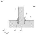
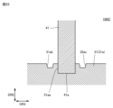
- It is an expanded sectional view of the power converter device 100B in the vicinity of the 3rd groove
- It is an expanded sectional view of the power converter device 100B in the vicinity of the 4th groove
- FIG. 10 is a plan view of a case 30 included in Modification 1 of power converter 100B.
- FIG. 11 is an enlarged cross-sectional view of Modified Example 2 of the power conversion device 100B in the vicinity of the first groove 31aa; It is an expanded sectional view of the modification 2 of the power converter device 100B in the vicinity of the 2nd groove
- 3 is an enlarged cross-sectional view of the power converter 100C in the vicinity of the bottom wall 32.
- FIG. 12 is an enlarged cross-sectional view of Modified Example 2 of the power conversion device 100C in the vicinity of the first groove 31aa; It is an expanded sectional view of the modification 2 of 100 C of electric power converters in the vicinity of 2nd groove
- FIG. 10 is a cross-sectional view of Modification 1 of power converter 100D.
- FIG. 11 is a cross-sectional view of a second modification of the power conversion device 100D;
- FIG. 11 is a cross-sectional view of a third modification of the power conversion device 100D; FIG.
- FIG. 11 is a cross-sectional view of a fourth modification of the power conversion device 100D; It is a side view of the 1st heat sink 41 which the power converter device 100E has. It is a side view of the 2nd heat sink 42 which the power converter device 100E has.
- 3 is an exploded perspective view of a printed wiring board 60 included in power converter 100F. FIG. It is a bottom view of the printed wiring board 60 which the power converter device 100G has.
- FIG. 34 is a schematic cross-sectional view along XXXIV-XXXIV in FIG. 33; FIG. 34 is a schematic cross-sectional view along XXXV-XXXV of FIG. 33;
- Embodiment 1 A power converter according to Embodiment 1 will be described.
- the power conversion device according to Embodiment 1 is referred to as power conversion device 100 .
- FIG. 1 is a circuit diagram of the power converter 100.
- the power converter 100 has a peripheral circuit 110 and a switching circuit 120 .
- the peripheral circuit 110 has a plurality of circuit components 10.
- the plurality of circuit components 10 are a capacitor 10a, an inductor 10b, a contactor 10c, a discharging resistor 10d and a charging resistor 10e.
- Capacitor 10a, inductor 10b and contactor 10c are connected in series.
- Inductor 10b is arranged between capacitor 10a and contactor 10c.
- a discharging resistor 10d and a charging resistor 10e are connected in parallel to the capacitor 10a and the contactor 10c, respectively.
- Peripheral circuit 110 is connected to DC supply circuit 130 .
- the switching circuit 120 is, for example, a three-phase inverter circuit.
- the switching circuit 120 has multiple circuit components 20 .
- the plurality of circuit components 20 are transistors 20a-20f and diodes 20g-20l.
- the drain of the transistor 20a is electrically connected to one electrode of the capacitor 10a.
- the source of transistor 20a is electrically connected to the drain of transistor 20b.
- the source of transistor 20b is electrically connected to the other electrode of capacitor 10a.
- the anode of diode 20g is electrically connected to the source of transistor 20a.
- the cathode of diode 20g is electrically connected to the drain of transistor 20a.
- the anode of diode 20h is electrically connected to the source of transistor 20b.
- the cathode of diode 20h is electrically connected to the drain of transistor 20b.
- the transistor 20c, the transistor 20d, the diode 20i and the diode 20j are connected in the same manner as the transistor 20a, the transistor 20b, the diode 20g and the diode 20h, respectively.
- Transistor 20e, transistor 20f, diode 20k, and diode 20l are connected in the same manner as transistor 20a, transistor 20b, diode 20g, and diode 20h, respectively.
- the gates of transistors 20a-20f are connected to a control circuit.
- the switching circuit 120 is connected to the motor 140.
- Motor 140 is, for example, a three-phase motor.
- Motor 140 has input line 141 , input line 142 , and input line 143 .
- the input line 141 is electrically connected to the source of the transistor 20a and the drain of the transistor 20b.
- the input line 142 is electrically connected to the source of the transistor 20c and the drain of the transistor 20d.
- the input line 143 is electrically connected to the source of the transistor 20e and the drain of the transistor 20f.
- FIG. 2 is a perspective view of the power converter 100.
- FIG. FIG. 3 is an exploded perspective view of the power conversion device 100.
- FIG. FIG. 4 is a cross-sectional view along IV-IV in FIG.
- FIG. 5 is a plan view of the case 30 included in the power conversion device 100.
- FIG. FIG. 6 is a bottom view of the printed wiring board 60 included in the power conversion device 100.
- FIG. 7 is a side view of the first radiator plate 41 included in the power converter 100.
- FIG. FIG. 8 is a side view of the second radiator plate 42 included in the power conversion device 100.
- the power converter 100 includes a plurality of circuit components 10, a case 30, a plurality of first heat sinks 41 and a plurality of second heat sinks 42, and a sealing material 50. , and a printed wiring board 60 .
- the case 30 has side walls 31 and a bottom wall 32 .
- a direction along the normal to the inner wall surface of the bottom wall 32 is defined as a first direction DR1.
- a direction perpendicular to the first direction DR1 is defined as a second direction DR2.
- a direction perpendicular to the first direction DR1 and the second direction DR2 is defined as a third direction DR3.
- the side wall 31 has, for example, a rectangular shape in plan view.
- the side wall 31 has a first side wall portion 31a and a second side wall portion 31b, and a third side wall portion 31c and a fourth side wall portion 31d.
- the first side wall portion 31a and the second side wall portion 31b face each other with a gap therebetween in the second direction DR2.
- the third side wall portion 31c and the fourth side wall portion 31d face each other with a gap therebetween in the third direction DR3.
- the arithmetic average roughness of the inner wall surface of the side wall 31 is preferably 6.3 ⁇ m or more.
- the bottom wall 32 continues to the lower ends of the side walls 31 .
- the case 30 is made of rigid material. Case 30 is made of, for example, a metal material.
- the case 30 is made of copper (Cu), a copper alloy, aluminum (Al), an aluminum alloy, iron (Fe), an iron alloy, or the like.
- the case 30 may be made of a resin material.
- a plurality of first grooves 31aa are formed in the inner wall surface of the first side wall portion 31a.
- the multiple first grooves 31aa are arranged at intervals in the third direction DR3.
- the first groove 31aa extends along the first direction DR1. Both ends of the first groove 31aa in the third direction DR3 reach the upper end and lower end of the first side wall portion 31a, respectively.
- a plurality of second grooves 31ba are formed in the inner wall surface of the second side wall portion 31b.
- the plurality of second grooves 31ba are arranged at intervals in the third direction DR3.
- the second groove 31ba extends along the first direction DR1. Both ends of the second groove 31ba in the third direction DR3 reach the upper end and lower end of the second side wall portion 31b, respectively.
- the second groove 31ba faces the first groove 31aa in the second direction DR2.
- the first heat sink 41 and the second heat sink 42 are arranged inside the case 30 . More specifically, the first heat sink 41 and the second heat sink 42 are arranged in a space defined by the side walls 31 and the bottom wall 32 .
- the first heat sink 41 and the second heat sink 42 are made of a material with high thermal conductivity.
- the first heat sink 41 and the second heat sink 42 are made of, for example, copper, copper alloy, aluminum, aluminum alloy, iron, iron alloy, or the like.
- the first radiator plate 41 and the second radiator plate 42 may be made of the same material or may be made of different materials.
- the arithmetic average roughness of the side surfaces of the first heat sink 41 and the second heat sink 42 is preferably 6.3 ⁇ m or more.
- the first heat sink 41 extends along the second direction DR2 in plan view.
- the multiple first heat sinks 41 are arranged at intervals in the third direction DR3.
- the first heat sink 41 has a first end 41a and a second end 41b in the second direction DR2.
- the second end 41b is the end opposite to the first end 41a.
- the first heat sink 41 is attached to the case 30 by inserting the first end 41a and the second end 41b into the first groove 31aa and the second groove 31ba, respectively.
- the first radiator plate 41 faces the electrode surface 11a.
- the first heat sink 41 has a third end 41c and a fourth end 41d in the first direction DR1.
- the third end 41c is on the bottom wall 32 side.
- the third end 41c is thermally connected to the bottom wall 32 via a heat radiation auxiliary member 51, which will be described later.
- the fourth end 41d is the end opposite to the third end 41c.
- the first radiator plate 41 is formed with a plurality of first insertion openings 41e.
- the first insertion port 41e penetrates the first heat sink 41 along the thickness direction.
- the first insertion port 41e extends from the fourth end 41d toward the third end 41c.
- the number of first insertion openings 41 e is equal to or greater than the number of second heat sinks 42 .
- the second radiator plate 42 extends along the third direction DR3 in plan view.
- the multiple second radiator plates 42 are arranged at intervals in the second direction DR2.
- the second heat sink 42 has a fifth end 42a and a sixth end 42b in the first direction DR1.
- the fifth end 42a is on the bottom wall 32 side.
- the sixth end 42b is the end opposite to the fifth end 42a.
- the second radiator plate 42 is formed with a plurality of second insertion openings 42c.
- the second insertion port 42c penetrates the second heat sink 42 along the thickness direction.
- the second insertion port 42c extends from the fifth end 42a toward the sixth end 42b.
- the number of second insertion openings 42c is greater than or equal to the number of first radiator plates 41.
- the second radiator plate 42 is attached to the first radiator plate 41 by inserting the second insertion port 42c into the first insertion port 41e.
- the first heat radiation plate 41 and the second heat radiation plate 42 are assembled in a grid shape in plan view.
- the inner wall surface of the third side wall portion 31c is formed with a plurality of grooves extending along the first direction DR1 and spaced apart in the second direction DR2. may be Further, a plurality of grooves extending along the first direction DR1 and spaced apart in the second direction DR2 may be formed in the inner wall surface of the fourth side wall portion 31d.
- the second heat sink 42 has grooves formed in the inner wall surface of the third side wall portion 31c and grooves formed in the inner wall surface of the fourth side wall portion 31d at both ends of the second heat sink 42 in the third direction DR3. may be attached to the case 30 by being inserted into the
- the second heat sink 42 has a seventh end 42e and an eighth end 42f in the third direction DR3.
- the eighth end 42f is the end opposite to the seventh end 42e.
- the seventh end 42e and the eighth end 42f are preferably separated from the inner wall surface of the third side wall portion 31c and the inner wall surface of the fourth side wall portion 31d, respectively.
- the molding material 52 is provided between the seventh end 42e and the inner wall surface of the third side wall portion 31c and between the eighth end 42f and the inner wall surface of the fourth side wall portion 31d. is preferably arranged.
- the inner wall surface of the third side wall portion 31c is provided with the seventh edge.
- a groove into which the eighth end 42f is inserted may be formed in the inner wall surface of the fourth side wall portion 31d while a groove into which the eighth end 42f is inserted is formed.
- the circuit component 10 is a capacitor 10a.
- the capacitor 10 a is arranged in a space defined by two adjacent first heat sinks 41 , two adjacent second heat sinks 42 and the bottom wall 32 .
- the capacitor 10a is, for example, a film capacitor.
- the circuit component 10 has an element body and lead wires.
- the element body is the capacitor element body 11 and the lead wire is the lead wire 12 .
- Capacitor 10 a further includes exterior case 13 and sealing resin 14 .
- the capacitor element body 11 is configured, for example, by winding a metal film and a dielectric film placed on the metal film. Both end surfaces of the capacitor element body 11 are electrode surfaces 11a.
- a lead wire 12 is electrically connected to the electrode surface 11a.
- the lead wire 12 plays a role of allowing current from the outside to flow through the capacitor element body 11 .
- the lead wire 12 is made of a conductive material such as a metal material.
- the capacitor element main body 11 has two electrode surfaces 11a.
- the two electrode surfaces 11 a are opposed to two separate first heat sinks 41 with the molding material 52 interposed therebetween.
- the exterior case 13 is made of an insulating material.
- the exterior case 13 is made of, for example, a resin material.
- the capacitor element main body 11 and lead wires 12 are housed in an exterior case 13 . However, part of the lead wire 12 protrudes from the upper surface of the exterior case 13 .
- the sealing resin 14 is filled in the exterior case 13 .
- the plurality of capacitors 10a are arranged in first and second rows.
- the first row and the second row are along the second direction DR2.
- the electrode surfaces 11a of the capacitors 10a belonging to the first row preferably face the electrode surfaces 11a of the capacitors 10a belonging to the second row.
- a first radiator plate 41 is arranged between the first row and the second row. That is, the electrode surface 11a of the capacitor 10a belonging to the first row faces the electrode surface 11a of the capacitor 10a belonging to the second row with the first heat sink 41 interposed therebetween.
- the sealing material 50 is filled inside the case 30 . More specifically, the sealing material 50 fills the space defined by the two adjacent first heat sinks 41 , the two adjacent second heat sinks 42 and the bottom wall 32 .
- the encapsulating material 50 has a heat radiation assisting material 51 and a mold material 52 .
- the auxiliary heat dissipation material 51 is, for example, a resin material such as silicone resin, epoxy resin, or urethane resin, grease, gel, or an insulating sheet.
- the heat-dissipating auxiliary material 51 may contain a heat-conducting filler.
- the thermally conductive filler is made of, for example, ceramics or metal material.
- the thermal conductivity of the auxiliary heat dissipation material 51 is, for example, 1 W/m ⁇ K or more and several tens of W/m ⁇ K or less.
- the auxiliary heat dissipation material 51 is applied on the bottom wall 32 . More specifically, the auxiliary heat dissipation material 51 is applied on the inner wall surface of the bottom wall 32 .
- the auxiliary heat dissipation material 51 may also be applied on the first grooves 31aa and the second grooves 31ba.
- the molding material 52 is, for example, a resin material with high thermal conductivity.
- the molding material 52 is, for example, an epoxy resin, a silicone resin, or a urethane resin containing a thermally conductive filler.
- the thermal conductivity of the molding material 52 is, for example, 0.1 W/m ⁇ K or more and 20 W/m ⁇ K or less.
- the Young's modulus of the molding material 52 is, for example, 1 MPa or more and 50 GPa or less.
- the molding material 52 may be made of the same material as the auxiliary heat dissipation material 51 .
- the auxiliary heat dissipation material 51 and the molding material 52 may be an adhesive.
- the molding material 52 is arranged on the auxiliary heat dissipation material 51 .
- the molding material 52 is in contact with the bottom, side and top surfaces of the exterior case 13 . That is, the molding material 52 surrounds the capacitor 10a. Note that the lead wire 12 protrudes from the molding material 52 .
- the molding material 52 is also in contact with the inner wall surface of the side wall 31 , the side surface of the first heat sink 41 and the side surface of the second heat sink 42 .
- the printed wiring board 60 has a first surface 60a and a second surface 60b.
- the first surface 60a faces the case 30 side.
- the second surface 60b is the opposite surface of the first surface 60a.
- Capacitor 10 a is electrically connected to printed wiring board 60 . More specifically, the capacitor 10 a is connected to the printed wiring board 60 by inserting the lead wires 12 into through holes (not shown) formed in the printed wiring board 60 and soldering them. Thus, the wiring of the peripheral circuit 110 shown in FIG. 1 is realized.
- Capacitor 10a and printed wiring board 60 may be connected using a conductive adhesive.
- the printed wiring board 60 also has external connection terminals 60c.
- the external connection terminal 60c is composed of a land and is connected to the switching circuit 120 shown in FIG. 1 by being energized in contact with a bus bar (not shown).
- a printed wiring board 60 is attached to the upper end of the side wall 31 .
- FIG. 9 is a schematic side view when connecting a plurality of power converters 100.
- One of the plurality of power electronics devices 100 is assumed to be a power electronics device 101
- the other one of the plurality of power electronics devices 100 is assumed to be a power electronics device 102 .
- the power electronics device 101 and the power electronics device 102 are connected by a connection member 61 .
- the connection member 61 has one end connected to the external connection terminal 60c of the printed wiring board 60 of the power conversion device 101, and the other end connected to the external connection terminal 60c of the printed wiring board 60 of the power conversion device 102. It is connected.
- the connection member 61 is, for example, a rolled material made of a metal material.
- FIG. 9 shows an example in which a plurality of power converters 100 are connected along the first direction DR1, the plurality of power converters 100 are connected along the second direction DR2 or the third direction DR3. may be connected via
- FIG. 10 is a plan view of the case 30 included in Modification 1 of the power converter 100.
- a plurality of grooves 31 e may be formed in the outer wall surface of the side wall 31 .
- the groove 31e extends, for example, along the first direction DR1. In this case, the surface area of the outer wall surface of the side wall 31 is increased, and the thermal resistance between the case 30 and the outside air is reduced, so that the temperature rise of the capacitor 10a can be further suppressed.
- FIG. 11 is a cross-sectional view of Modification 2 of power conversion device 100 .
- FIG. 11 shows a cross section at a position corresponding to IV-IV in FIG.
- the sealing material 50 may have a silicone gel 53 instead of the molding material 52 .
- the silicone gel 53 preferably has low viscosity and high insulating properties.
- the silicone gel 53 Since the silicone gel 53 has high adhesion to the capacitor 10a, the first heat sink 41, and the second heat sink 42, the boundary between the capacitor 10a, the first heat sink 41, and the second heat sink 42 is evaluated in the insulation evaluation. There is no need to consider creepage at Therefore, in this case, an insulating area for securing the creepage distance is not required, and the size of the periphery of the capacitor 10a can be reduced. Further, in this case, heat generated by the capacitor 10 a can be efficiently transmitted to the case 30 . Furthermore, the silicone gel 53 is a highly penetrating, ie, soft material. Therefore, in this case, the reliability can be improved when the power conversion device 100 is subjected to a heat cycle or a power cycle. Since the position of the capacitor 10a is also fixed by attaching the printed wiring board 60 to the case 30, even if the penetration of the silicone gel 53 is high, the position of the capacitor 10a is not hindered.
- the case 30, the plurality of first radiator plates 41, the plurality of second radiator plates 42, and the printed wiring board 60 to which the plurality of capacitors 10a are connected are prepared.
- a heat dissipation auxiliary material 51 is applied on the inner wall surface of the bottom wall 32 .
- the auxiliary heat dissipation material 51 may be applied also on the first groove 31aa and the second groove 31ba.
- the first heat sink 41 is attached to the case 30 .
- the first heat sink 41 is attached by inserting the first end 41a and the second end 41b into the first groove 31aa and the second groove 31ba, respectively.
- the second heat sink 42 is attached to the first heat sink 41 .
- the second radiator plate 42 is attached by inserting the second insertion port 42c into the first insertion port 41e.
- the molding material 52 is injected into the case 30 .
- a printed wiring board 60 is attached to the top edge of the side wall 31 .
- the capacitor 10 a is arranged in the space defined by the two adjacent first heat sinks 41 , the two adjacent second heat sinks 42 and the bottom wall 32 and is surrounded by the molding material 52 .
- the mold material 52 is cured. As described above, the assembly of the power converter 100 is completed.
- ⁇ Modification 1 of method for assembling power conversion device 100> When the auxiliary heat dissipation material 51 and the molding material 52 are made of the same material, the sealing material 50 is injected into the case 30 before the first heat radiation plate 41 is attached to the case 30 in the assembly of the power conversion device 100 . good too. In this case, the number of assembly procedures is reduced, so the time required for assembly can be reduced.
- ⁇ Modification 2 of the method for assembling the power conversion device 100> In the assembly of the power conversion device 100, the application of the auxiliary heat dissipation material 51 is performed after the first heat dissipation plate 41 is attached to the case 30 and the second heat dissipation plate 42 is attached to the first heat dissipation plate 41. It may be performed prior to the injection of material 52 . In this case, the first heat dissipation plate 41 contacts the bottom wall 32 without the auxiliary heat dissipation member 51 interposed therebetween.
- the sealing material 50 may be injected after the printed wiring board 60 is attached to the case 30 in assembling the power conversion device 100 . Injection of the sealing material 50 is performed from an injection port previously formed in the printed wiring board 60 . In this case, the number of assembly procedures is reduced, so the time required for assembly can be reduced.
- a plurality of capacitors 10a are densely arranged. Therefore, if the heat generation of the capacitor 10a interferes with each other and the temperature of the capacitor 10a rises excessively, there is a risk that the characteristics of the capacitor 10a will be degraded, destroyed, and the life of the capacitor 10a shortened.
- the capacitor 10a is thermally connected to the case 30 by the sealing material 50, the first radiator plate 41 and the second radiator plate . Therefore, according to the power conversion device 100, the heat generated by the capacitor 10a is radiated from the case 30 to the outside air, and the temperature rise of the capacitor 10a is suppressed.
- the life of the capacitor 10a is lengthened. For example, if the temperature of the capacitor 10a drops by 10° C., the life of the capacitor 10a is approximately doubled.
- the life of the enamel coating of the inductor 10b is approximately doubled by decreasing the temperature of the inductor 10b by 10°C.
- the circuit component 10 is the discharging resistor 10d or the charging resistor 10e
- the power category rank of the discharging resistor 10d or the charging resistor 10e can be lowered due to temperature derating. The number of series or parallel can be reduced.
- the heat generated by the capacitor 10a is transmitted to the first radiator plate 41 through the molding material 52.
- the heat transmitted to the first heat radiation plate 41 is transmitted to the side wall 31 from the first end 41a and the second end 41b, and is also transmitted to the bottom wall 32 from the third end 41c through the auxiliary heat radiation member 51.
- the area of the heat transfer path from the capacitor 10a to the case 30 is large, and the thermal resistance from the capacitor 10a to the case 30 is reduced, so the temperature rise of the capacitor 10a is suppressed.
- the two electrode surfaces 11a of the capacitor 10a are opposed to the two separate first heat sinks 41 via the molding material 52, so that the temperature rise of the capacitor 10a can be further suppressed. .
- the first insertion port 41e is formed at the fourth end 41d. That is, the first insertion port 41e is not formed at the third end 41c. Therefore, the heat transfer area between the first heat radiation plate 41 and the bottom wall 32 is increased, and the thermal resistance between the first heat radiation plate 41 and the bottom wall 32 is decreased, thereby further suppressing the temperature rise of the capacitor 10a. can do.
- the power converter 100 has a second heat sink 42 thermally connected to the first heat sink 41 in addition to the first heat sink 41 . Therefore, in the power conversion device 100, the heat transmitted from the capacitor 10a to the first heat sink 41 through the molding material 52 is also transmitted to the case 30 through the second heat sink 42, and the temperature rise of the capacitor 10a further increases. Suppressed.
- the first radiator plate 41 extends along the second direction DR2 and the plurality of capacitors 10a are arranged along the second direction DR2.
- the temperature difference between the plurality of capacitors 10a that are in the state is reduced.
- the second radiator plate 42 extends along the third direction DR3 and the plurality of capacitors 10a are arranged along the third direction DR3.
- the temperature difference between the plurality of capacitors 10a arranged along the line is reduced.
- the temperature rise of the capacitor 10a differs depending on its position. More specifically, the capacitor 10a arranged near the center of the power conversion device 100 is affected by the heat generated by the capacitors 10a arranged around it, so that the capacitor 10a arranged near the outer periphery of the power conversion device 100 Temperature rises more easily than 10a. Temperature derating is determined by the hottest capacitor 10a. As described above, in the power conversion device 100, the temperature is made uniform among the plurality of capacitors 10a by the first heat dissipation plate 41 and the second heat dissipation plate 42, so that the power conversion device 100 can be used more effectively. can. Moreover, in the power conversion device 100, as a result of equalizing the temperatures among the plurality of capacitors 10a, the number of series or parallel connections of the capacitors 10a can be reduced.
- either the first heat sink 41 or the second heat sink 42 is arranged between two adjacent capacitors 10a. Therefore, the first radiator plate 41 and the second radiator plate 42 function as firewalls. That is, even if discharge sparks and impact are generated due to a failure of a certain capacitor 10a, the sparks and impact are prevented from reaching the other capacitors 10a by the first heat sink 41 and the second heat sink .
- the circuit component 10 is the inductor 10b, since the leakage magnetic flux from the inductor 10b to the surroundings is shielded by the first heat sink 41 and the second heat sink 42, sensor components (for example, Hall effect It is possible to improve the accuracy of the current sensor used).
- the sealing material 50 is filled in the case 30, the vibration resistance of the capacitor 10a is improved.
- the arithmetic average roughness of the inner wall surface of the side wall 31, the side surface of the first radiator plate 41, and the side surface of the second radiator plate 42 is 6.3 ⁇ m or more, the adhesion with the sealing material 50 is improved. Therefore, the mechanical strength of the power converter 100 is improved.
- the two adjacent first heat sinks 41 and the two adjacent second heat sinks 42 form a grid shape.
- the number or size of the compartments provided can be increased or decreased to match the number or size of the capacitors 10a.
- the thickness, type, material, etc. of the first heat sink 41 and the second heat sink 42 can be arbitrarily selected.
- the first heat sink 41 and the second heat sink 42 are subjected to bending or uneven press processing to ensure the strength of the first heat sink 41 and the second heat sink 42, and to form a grid shape. changes in the shape of the compartments are possible. In this way, the power conversion device 100 can flexibly implement various specifications at low cost.
- the temperature of the capacitor 10a tends to rise on the electrode surface 11a where current concentrates.
- the electrode surface 11a faces the first heat sink 41 (or the second heat sink 42)
- the heat generated on the electrode surface 11a is dissipated through the first heat sink 41 (or the second heat sink 42). ) to the case 30, thereby further suppressing the temperature rise of the capacitor 10a.
- the molding material 52 is separated from the seventh end 42e and the third side wall portion. 31c and between the eighth end 42f and the fourth side wall portion 31d. It becomes easy to be transmitted to.
- the seventh end 42e and the eighth end 42f are located inside the inner wall surface of the third side wall portion 31c and the inner wall surface of the fourth side wall portion 31d, respectively.
- the second radiator plate 42 may bend and break unless the dimensional tolerances of the first insertion port 41e and the second insertion port 42c are strictly controlled.
- Embodiment 2 A power converter according to Embodiment 2 will be described.
- the power conversion device according to Embodiment 2 is referred to as a power conversion device 100A.
- points different from the power conversion device 100 will be mainly described, and redundant description will not be repeated.
- the power conversion device 100A includes a plurality of circuit components 10, a case 30, a plurality of first heat sinks 41 and a plurality of second heat sinks 42, a sealing material 50, and a printed wiring board 60. . Regarding this point, the configuration of the power conversion device 100A is common to the configuration of the power conversion device 100 .
- FIG. 12 is a plan view of the case 30 included in the power converter 100A.
- FIG. 13 is an enlarged cross-sectional view of the power converter 100A in the vicinity of the third groove 32a.
- FIG. 13 shows an enlarged cross section orthogonal to the second direction DR2.
- FIG. 14 is an enlarged cross-sectional view of the power converter 100A in the vicinity of the fourth groove 32b.
- FIG. 14 shows an enlarged cross section perpendicular to the third direction DR3.
- the inner wall surface of the bottom wall 32 is formed with a plurality of third grooves 32a and a plurality of fourth grooves 32b.
- the third groove 32a extends along the second direction DR2.
- the multiple third grooves 32a are arranged at intervals in the third direction DR3.
- the third end 41c side of the first radiator plate 41 is inserted into the third groove 32a.
- the fourth groove 32b extends along the third direction DR3.
- the multiple fourth grooves 32b are arranged at intervals in the second direction DR2.
- the fifth end 42a side of the second radiator plate 42 is inserted into the fourth groove 32b.
- the third groove 32a and the fourth groove 32b may or may not be filled with the sealing material 50 . Regarding these points, the configuration of the power conversion device 100A is different from the configuration of the power conversion device 100 .
- the first heat sink 41 is inserted into the third groove 32a and the second heat sink 42 is inserted into the fourth groove 32b. and the bottom wall 32 is increased, and the thermal resistance between the first and second heat sinks 41 and 42 and the bottom wall 32 is reduced. As a result, according to the power conversion device 100A, it is possible to further suppress the temperature rise of the capacitor 10a.
- the first heat sink 41 is inserted into the third groove 32a and the second heat sink 42 is inserted into the fourth groove 32b.
- the assemblability and positioning accuracy of the plate 42 are improved.
- the distance between the first heat sink 41 and the second heat sink 42 and the capacitor 10a can be set with high accuracy, and the sealing is improved.
- the thermal resistance between the capacitor 10a and the first heat sink 41 and the second heat sink 42 can be reduced.
- the first heat sink 41 and the second heat sink 42 are fixed to the bottom wall 32, so that two adjacent first heat sinks 41, two adjacent second heat sinks 42 and The space defined by the bottom wall 32 can be more reliably filled with the sealing material 50 .
- Embodiment 3 A power converter according to Embodiment 3 will be described.
- the power conversion device according to Embodiment 3 is referred to as a power conversion device 100B.
- points different from the power conversion device 100A will be mainly described, and redundant description will not be repeated.
- the power conversion device 100B includes a plurality of circuit components 10, a case 30, a plurality of first heat sinks 41 and a plurality of second heat sinks 42, a sealing material 50, and a printed wiring board 60. . Regarding this point, the configuration of the power conversion device 100B is common to the configuration of the power conversion device 100A.
- FIG. 15 is an enlarged cross-sectional view of the power converter 100B in the vicinity of the third groove 32a.
- FIG. 15 shows an enlarged cross section perpendicular to the second direction DR2.
- FIG. 16 is an enlarged cross-sectional view of the power conversion device 100B in the vicinity of the fourth groove 32b.
- FIG. 16 shows an enlarged cross section perpendicular to the third direction DR3.
- the first heat sink 41 is metal-bonded to the third groove 32a on the third end 41c side.
- the second heat sink 42 is metal-bonded to the fourth groove 32b on the fifth end 42a side.
- first heat sink 41 does not have to be metal-bonded to the third groove 32a at all the portions inserted into the third grooves 32a, and the second heat sink 42 is inserted into the fourth grooves 32b. Not all parts need to be metal-bonded to the fourth groove 32b.
- the metal bonding between the first heat radiation plate 41 and the third groove 32a and the metal bonding between the second heat radiation plate 42 and the fourth groove 32b are performed by the brazing material 33, for example.
- Metal bonding between the first heat sink 41 and the third groove 32a and metal bonding between the second heat sink 42 and the fourth groove 32b may be performed by welding.
- the configuration of the power conversion device 100B is different from the configuration of the power conversion device 100A.
- the first heat sink 41 is metal-bonded to the third groove 32a and the second heat sink 42 is metal-bonded to the fourth groove 32b.
- the thermal resistance between plate 42 and bottom wall 32 is reduced.
- the first heat sink 41 is metal-bonded to the third groove 32a and the second heat sink 42 is metal-bonded to the fourth groove 32b.
- the assemblability and positioning accuracy of the heat sink 42 are improved.
- the distance between the first heat sink 41 and the second heat sink 42 and the capacitor 10a can be set with high accuracy, and the sealing is improved.
- the thermal resistance between the capacitor 10a and the first heat sink 41 and the second heat sink 42 can be reduced.
- the first heat sink 41 and the second heat sink 42 are fixed to the bottom wall 32, so that two adjacent first heat sinks 41, two adjacent second heat sinks 42 and The space defined by the bottom wall 32 can be more reliably filled with the sealing material 50 .
- FIG. 17 is a plan view of the case 30 included in Modification 1 of the power converter 100B.
- the third groove 32a may be widened at the portion where it intersects the fourth groove 32b, and the fourth groove 32b intersects with the third groove 32a. It may be widened in the part where it is.
- the third groove 32a may be widened at the end in the second direction DR2, and the fourth groove 32b may be widened at the end in the third direction DR3.
- the widened portions of the third groove 32a and the fourth groove 32b become pools of brazing filler metal, and the brazing filler metal 33 can be prevented from overflowing the third groove 32a and the fourth groove 32b to cause poor connection.
- FIG. 18 is an enlarged cross-sectional view of Modification 2 of power conversion device 100B in the vicinity of first groove 31aa.
- FIG. 19 is an enlarged cross-sectional view of Modification 2 of power conversion device 100B in the vicinity of second groove 31ba.
- 18 and 19 show enlarged cross sections orthogonal to the first direction DR1.
- the first heat sink 41 may be metal-bonded to the first groove 31aa on the side of the first end 41a, and may be metal-bonded to the side of the second end 41b. It may be metal-bonded to the second groove 31ba.
- Metal bonding between the first radiator plate 41 and the first grooves 31aa and the second grooves 31ba is performed by a brazing material 33, for example.
- Metal joining between the first heat sink 41 and the first grooves 31aa and the second grooves 31ba may be performed by welding. In this case, the thermal resistance between the first radiator plate 41 and the side wall 31 is reduced, so that the temperature rise of the capacitor 10a can be further suppressed.
- Embodiment 4 A power converter according to Embodiment 4 will be described.
- the power conversion device according to Embodiment 4 is referred to as a power conversion device 100C.
- points different from the power conversion device 100A will be mainly described, and redundant description will not be repeated.
- the power conversion device 100C includes a plurality of circuit components 10, a case 30, a plurality of first heat sinks 41 and a plurality of second heat sinks 42, a sealing material 50, and a printed wiring board 60. . Regarding this point, the configuration of the power conversion device 100C is common to the configuration of the power conversion device 100A.
- FIG. 20 is an enlarged cross-sectional view of the power converter 100C in the vicinity of the third groove 32a.
- FIG. 20 shows an enlarged cross section orthogonal to the second direction DR2.
- FIG. 21 is an enlarged cross-sectional view of the power converter 100C in the vicinity of the fourth groove 32b.
- FIG. 21 shows an enlarged cross section perpendicular to the third direction DR3.
- the first heat sink 41 is metal-bonded to the third groove 32a by caulking on the third end 41c side.
- the second heat sink 42 is metal-bonded to the fourth groove 32b by caulking on the fifth end 42a side.
- the inner wall surface of the bottom wall 32 is formed with caulked grooves 32ca and 32cb.
- the caulked grooves 32ca and the caulked grooves 32cb extend along the second direction DR2.
- the third groove 32a is arranged between the crimped groove 32ca and the crimped groove 32cb in the third direction DR3.
- the inner wall surface of the bottom wall 32 is formed with a caulked groove 32da and a caulked groove 32db.
- the caulking groove 32da and the caulking groove 32db extend along the third direction DR3.
- the fourth groove 32b is arranged between the caulking groove 32da and the caulking groove 32db in the second direction DR2.
- first heat sink 41 may not be crimped into the third groove 32a at all the portions inserted into the third grooves 32a, and the second heat sink 42 may not be crimped entirely into the fourth grooves 32b. portion may not be crimped to the fourth groove 32b.
- the configuration of the power conversion device 100C is different from the configuration of the power conversion device 100A.
- the first heat sink 41 is metal-bonded to the third groove 32a and the second heat sink 42 is metal-bonded to the fourth groove 32b by caulking. Thermal resistance between the second heat sink 42 and the bottom wall 32 is reduced. As a result, according to the power converter 100C, the temperature rise of the capacitor 10a can be further suppressed.
- the first heat sink 41 is metal-bonded to the third groove 32a and the second heat sink 42 is metal-bonded to the fourth groove 32b by caulking.
- the assemblability and positioning accuracy of 41 and second heat sink 42 are improved.
- the distance between the first heat sink 41 and the second heat sink 42 and the capacitor 10a can be set with high accuracy, and the sealing is improved.
- the thermal resistance between the capacitor 10a and the first heat sink 41 and the second heat sink 42 can be reduced.
- the first heat sink 41 and the second heat sink 42 are fixed to the bottom wall 32, so that two adjacent first heat sinks 41, two adjacent second heat sinks 42 and The space defined by the bottom wall 32 can be more reliably filled with the sealing material 50 .
- FIG. 22 is an enlarged cross-sectional view of the power conversion device 100C in the vicinity of the bottom wall 32.
- FIG. 22 shows an enlarged cross section orthogonal to the second direction DR2.
- the outer wall surface of the bottom wall 32 may be formed with a plurality of fifth grooves 32e.
- the fifth groove 32e extends along the second direction DR2.
- the multiple fifth grooves 32e are arranged at intervals in the third direction DR3.
- the fifth groove 32e may extend along the third direction DR3.
- the plurality of fifth grooves 32e are arranged at intervals in the second direction DR2.
- the outer wall surface of the bottom wall 32 may be further formed with caulked grooves 32ea and 32eb.
- the caulking grooves 32ea and the caulking grooves 32eb extend along the second direction DR2.
- the fifth groove 32e is arranged between the crimped grooves 32ea and the crimped grooves 32eb. Note that when the fifth groove 32e extends along the third direction DR3, the caulking grooves 32ea and the caulking grooves 32eb extend along the third direction DR3.
- the power conversion device 100C may have a plurality of plate members 34.
- the plate member 34 is inserted into the fifth groove 32e and crimped to the fifth groove 32e.
- the crimping of the plate member 34 to the fifth groove 32e is performed by inserting a press tool into the crimping grooves 32ea and 32eb. Since the plate member 34 crimped into the fifth groove 32e functions as a cooling fin, the heat dissipation from the case 30 to the outside air is improved, and the temperature rise of the capacitor 10a can be further suppressed.
- FIG. 23 is an enlarged cross-sectional view of Modification 2 of power conversion device 100C in the vicinity of first groove 31aa.
- FIG. 24 is an enlarged cross-sectional view of Modification 2 of power conversion device 100C in the vicinity of second groove 31ba. 23 and 24 show enlarged cross sections orthogonal to the first direction DR1.
- the first heat sink 41 may be metal-bonded to the first groove 31aa on the first end 41a side by caulking, and the second end 41b It may be metal-bonded to the second groove 31ba on the side.
- the caulking grooves 31ab and the caulking grooves 31ac may be formed in the inner wall surface of the first side wall portion 31a.
- the caulking grooves 31bb and the caulking grooves 31bc may be formed in the inner wall surface of the second side wall portion 31b.
- the caulking grooves 31ab, the caulking grooves 31ac, the caulking grooves 31bb, and the caulking grooves 31bc extend along the first direction DR1.
- a first groove 31aa is arranged between the caulked grooves 31ab and 31ac
- a second groove 31ba is arranged between the caulked grooves 31bb and 31bc.
- the first heat sink 41 is crimped into the first groove 31aa by inserting a press tool into the crimping grooves 31ab and 31ac, and is crimped into the second groove 31ba by inserting the press tool into the crimping grooves 31bb and 31bc. Crimped. In this case, the thermal resistance between the first radiator plate 41 and the side wall 31 is reduced, so that the temperature rise of the capacitor 10a can be further suppressed.
- Embodiment 5 A power converter according to Embodiment 5 will be described.
- the power conversion device according to Embodiment 5 is referred to as a power conversion device 100D.
- points different from the power conversion device 100 will be mainly described, and redundant description will not be repeated.
- the power conversion device 100D includes a plurality of circuit components 10, a case 30, a plurality of first heat sinks 41 and a plurality of second heat sinks 42, a sealing material 50, and a printed wiring board 60. . Regarding this point, the configuration of the power conversion device 100D is common to the configuration of the power conversion device 100 .
- FIG. 25 is a cross-sectional view of the power converter 100D.
- FIG. 25 shows a cross section at a position corresponding to IV-IV in FIG.
- capacitor 10a does not have exterior case 13 and sealing resin 14 .
- the power converter 100D further has an insulation net 70 .
- the insulating net 70 is a net-like member made of an insulating resin material.
- the insulating net 70 is made of, for example, epoxy resin, silicone resin, urethane resin, or the like.
- the insulating net 70 may be made of a flexible and stretchable rubber material.
- the insulating net 70 is arranged in the space defined by the two adjacent first heat sinks 41, the two adjacent second heat sinks 42 and the bottom wall 32 so as to surround the capacitor 10a. That is, the insulating net 70 is positioned between the capacitor 10 a and the first heat sink 41 , the second heat sink 42 and the bottom wall 32 . Although the insulating net 70 and the capacitor 10a are not in contact in the example shown in FIG. 25, the insulating net 70 may be in contact with the capacitor 10a. It is sufficient that the capacitor 10 a does not come into contact with the first radiator plate 41 , the second radiator plate 42 and the bottom wall 32 by the insulating net 70 .
- the encapsulant 50 does not have to have the auxiliary heat dissipation material 51 and the mold material 52.
- sealing material 50 may be formed by potting any resin material. Regarding these points, the configuration of the power conversion device 100D differs from the configuration of the power conversion device 100 .
- the capacitor 10a does not have the exterior case 13 and the sealing resin 14, so the number of turns of the metal film and the dielectric film in the capacitor 10a can be increased, and the number of turns per capacitor 10a can be increased. Increased capacitance is possible. Further, in the power conversion device 100D, the capacitor 10a does not have the exterior case 13 and the sealing resin 14, so the cost of the capacitor 10a can be reduced.
- the insulating net 70 is arranged between the capacitor 10a, the first heat sink 41, the second heat sink 42 and the bottom wall 32, the exterior case 13 and the sealing resin 14 are eliminated. Even so, insulation between the capacitor 10a and the first heat sink 41, the second heat sink 42, and the bottom wall 32 can be ensured.
- a resin material having a higher thermal conductivity than the sealing resin 14 can be used as the sealing material 50 , so heat generated by the capacitor 10 a can be efficiently transferred to the case 30 .
- FIG. 26 is a cross-sectional view of Modification 1 of power converter 100D.
- FIG. 26 shows a cross section at a position corresponding to IV-IV in FIG.
- an insulating paper 71 may be used instead of the insulating net .
- the insulating paper 71 is arranged in the space defined by the two adjacent first heat sinks 41, the two adjacent second heat sinks 42, and the bottom wall 32 so as to surround the capacitor 10a.
- FIG. 27 is a cross-sectional view of Modification 2 of the power converter 100D.
- FIG. 27 shows a cross section at a position corresponding to IV-IV in FIG.
- a heat-conducting insulating sheet 72 may be used instead of the insulating net 70 .
- the heat-conducting insulating sheet 72 is arranged in a space defined by two adjacent first heat radiation plates 41 , two adjacent second heat radiation plates 42 and the bottom wall 32 .
- FIG. 28 is a cross-sectional view of Modification 3 of the power converter 100D.
- FIG. 28 shows a cross section at a position corresponding to IV-IV in FIG.
- spacer 73 may be used instead of insulating net .
- the spacers 73 are arranged between the capacitor 10 a and the first heat sink 41 , between the capacitor 10 a and the second heat sink 42 , and between the capacitor 10 a and the bottom wall 32 .
- the spacer 73 is made of, for example, a resin material.
- FIG. 29 is a cross-sectional view of Modification 4 of power conversion device 100D.
- FIG. 29 shows a cross section at a position corresponding to IV-IV in FIG.
- sealing material 50 may be silicone gel 53 .
- the silicone gel 53 preferably has low viscosity and high insulating properties.
- the silicone gel 53 Since the silicone gel 53 has high adhesion to the capacitor 10a, the first heat sink 41, and the second heat sink 42, the boundary between the capacitor 10a, the first heat sink 41, and the second heat sink 42 is evaluated in the insulation evaluation. There is no need to consider creepage at Therefore, in this case, an insulating area for securing the creepage distance is not required, and the size of the periphery of the capacitor 10a can be reduced.
- the silicone gel 53 it is possible to ensure high insulation, that is, high creeping dielectric strength and penetration dielectric strength.
- the heat generated by the capacitor 10a can be efficiently transferred to the case 30.
- the silicone gel 53 is a highly penetrating, ie, soft material. Therefore, in this case, the reliability can be improved when the power conversion device 100 is subjected to a heat cycle or a power cycle. Since the position of the capacitor 10a is also fixed by attaching the printed wiring board 60 to the case 30, even if the penetration of the silicone gel 53 is high, the position of the capacitor 10a is not hindered.
- Embodiment 6 A power converter according to Embodiment 6 will be described.
- the power conversion device according to Embodiment 6 is referred to as a power conversion device 100E.
- points different from the power conversion device 100 will be mainly described, and redundant description will not be repeated.
- the power conversion device 100E includes a plurality of circuit components 10, a case 30, a plurality of first heat sinks 41 and a plurality of second heat sinks 42, a sealing material 50, and a printed wiring board 60. . Regarding this point, the configuration of the power conversion device 100E is common to the configuration of the power conversion device 100 .
- FIG. 30 is a side view of the first radiator plate 41 of the power converter 100E.
- the first heat sink 41 is formed with a plurality of through holes 41f.
- the through hole 41f penetrates the first radiator plate 41 along the thickness direction.
- the plurality of through holes 41f are arranged at intervals in the second direction DR2.
- the through hole 41f is arranged between two adjacent first insertion openings 41e.
- the width of the first insertion port 41e in the second direction DR2 is larger than the thickness of the second radiator plate 42.
- the width of the first insertion port 41e in the second direction DR2 should be greater than the thickness of the second radiator plate 42 by 0.1 mm or more. It is preferably 0.5 mm or more larger than the height.
- FIG. 31 is a side view of the second radiator plate 42 of the power converter 100E.
- the second radiator plate 42 is formed with a plurality of through holes 42d.
- 42 d of through-holes have penetrated the 2nd heat sink 42 along the thickness direction.
- 42 d of several through-holes are arrange
- 42 d of through-holes are arrange
- the width of the second insertion port 42c in the third direction DR3 is larger than the thickness of the first radiator plate 41.
- the width of the second insertion port 42c in the third direction DR3 should be greater than the thickness of the first heat sink 41 by 0.1 mm or more. It is preferably 0.5 mm or more larger than the height.
- the through hole 41f is formed in the first radiator plate 41
- the through hole 42d is formed in the second radiator plate 42
- the second direction DR2 of the first insertion port 41e is formed.
- at least one of the width in the third direction DR3 of the second insertion port 42c and the thickness of the first heat sink 41 sufficiently larger than the thickness of the second heat sink 42 as long as it is satisfied.
- the configuration of the power conversion device 100E is different from the configuration of the power conversion device 100 .
- the first radiator plate 41 is formed with a through hole 41f
- the second radiator plate 42 is formed with a through hole 42d. Therefore, the sealing material 50 is injected into the space defined by the two adjacent first heat sinks 41, the two adjacent second heat sinks 42, and the bottom wall 32 through the through holes 41f and 42d. easier to be As a result, voids are less likely to occur in the sealing material 50 in the space defined by the two adjacent first heat sinks 41 , the two adjacent second heat sinks 42 , and the bottom wall 32 .
- the lack of voids in the encapsulant 50 reduces the thermal resistance of the encapsulant 50 . Therefore, in the power conversion device 100E, it is possible to further suppress the temperature rise of the capacitor 10a.
- the sealing material 50 exists also in the through holes 41f and 42d. Therefore, in the power conversion device 100E, the adhesiveness between the sealing material 50 and the first heat sink 41 and the second heat sink 42 can be further improved. Further, in the power converter 100E, as a result of forming the through hole 41f and the through hole 42d, the amount of material used for forming the first heat sink 41 and the second heat sink 42 is reduced. The manufacturing cost and weight of 41 and second heat sink 42 can be reduced.
- the width of the first insertion port 41e in the second direction DR2 is sufficiently larger than the thickness of the second heat sink 42, and the width of the second insertion port 42c in the third direction DR3 is the width of the first heat sink 41e.
- the second heat sink 42 can be easily attached to the first heat sink 41 . Therefore, according to the power conversion device 100E, it is possible to improve the ease of assembly.
- Embodiment 7 A power converter according to Embodiment 7 will be described.
- the power conversion device according to Embodiment 7 is referred to as a power conversion device 100F.
- points different from the power conversion device 100 will be mainly described, and redundant description will not be repeated.
- the power conversion device 100F includes a plurality of circuit components 10, a case 30, a plurality of first heat sinks 41 and a plurality of second heat sinks 42, a sealing material 50, and a printed wiring board 60. . Regarding this point, the configuration of the power conversion device 100F is common to the configuration of the power conversion device 100 .
- FIG. 32 is an exploded perspective view of the printed wiring board 60 included in the power converter 100F.
- printed wiring board 60 has a plurality of laminated layers.
- the printed wiring board 60 has a four-layer structure including a first layer 60d, a second layer 60e, a third layer 60f, and a fourth layer 60g.
- the printed wiring board 60 is not limited to the four-layer structure.
- the first layer 60d, the second layer 60e, the third layer 60f, and the fourth layer 60g are laminated in this order from the first surface 60a toward the second surface 60b.
- each of the multiple layers forming the printed wiring board 60 has a wiring pattern.
- the wiring patterns of the first layer 60d, the second layer 60e, the third layer 60f and the fourth layer 60g are respectively the wiring pattern 60h, the wiring pattern 60i, the wiring pattern 60j and the wiring pattern 60k. be.
- a potential different from that applied to the wiring pattern 60i and the wiring pattern 60j is applied to the wiring pattern 60h and the wiring pattern 60j.
- Wiring patterns adjacent to each other in the thickness direction of printed wiring board 60 are insulated from each other.
- the wiring pattern 60h is preferably arranged near the portion where the side wall 31 and the printed wiring board 60 are in contact. Regarding these points, the configuration of the power conversion device 100F is different from the configuration of the power conversion device 100 .
- the power conversion device 100F since wiring patterns with different potentials are alternately stacked, stray capacitance occurs between layers. As a result, the required capacitance of the capacitor 10a can be compensated for by the stray capacitance of the printed wiring board 60, so that the number of series or parallel connections of the capacitor 10a can be reduced. In addition, in the power conversion device 100F, since the wiring patterns with different potentials are arranged in parallel, the inductance between the wiring patterns can be reduced. As a result, the surge voltage caused by switching of the switching circuit 120 can be reduced.
- the printed wiring board 60 When an alternating current flows through the printed wiring board 60 when the power conversion device 100F operates, power consumption occurs due to the resistance component of the printed wiring board 60, and the printed wiring board 60 generates heat.
- the wiring pattern 60h, the wiring pattern 60i, the wiring pattern 60j, and the wiring pattern 60k generate heat.
- the wiring pattern 60h is arranged near the portion where the side wall 31 and the printed wiring board 60 are in contact with each other, the temperature rise of the wiring pattern 60h can be suppressed.
- Embodiment 8 A power converter according to Embodiment 8 will be described.
- the power conversion device according to Embodiment 8 is referred to as a power conversion device 100G.
- points different from the power conversion device 100 will be mainly described, and redundant description will not be repeated.
- the power converter 100G includes a plurality of circuit components 10, a case 30, a plurality of first heat sinks 41 and a plurality of second heat sinks 42, a sealing material 50, and a printed wiring board 60. . Regarding this point, the configuration of the power conversion device 100G is common to the configuration of the power conversion device 100 .
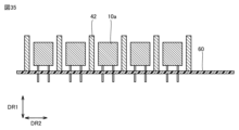
- FIG. 33 is a bottom view of the printed wiring board 60 included in the power converter 100G.
- 34 is a schematic cross-sectional view taken along line XXXIV-XXXIV of FIG. 33.
- FIG. 35 is a schematic cross-sectional view taken along line XXXV-XXXV of FIG. 33.
- FIG. As shown in FIGS. 33 to 35, in the power converter 100G, the first heat sink 41 and the second heat sink 42 are connected to the printed wiring board 60. As shown in FIG. The first heat sink 41 and the second heat sink 42 are connected to the printed wiring board 60 by soldering, for example. Regarding these points, the configuration of the power conversion device 100G differs from the configuration of the power conversion device 100 .
- the case 30 and the printed wiring board 60 to which the plurality of first heat sinks 41, the plurality of second heat sinks 42, and the plurality of capacitors 10a are connected are prepared.
- a sealing material 50 is injected into the case 30 .
- the printed wiring board 60 to which the plurality of first heat sinks 41, the plurality of second heat sinks 42, and the plurality of capacitors 10a are connected is attached to the case 30.
- the encapsulant 50 is cured. As described above, the assembly of the power conversion device 100G is completed.
- the first heat sink 41 and the second heat sink 42 are connected to the printed wiring board 60 in advance, the ease of assembly of the first heat sink 41 and the second heat sink 42 to the case 30 is improved. be done. Further, in the power conversion device 100G, since the positioning accuracy of the capacitor 10a, the first heat sink 41 and the second heat sink 42 is improved, the thickness of the sealing material 50 is reduced so that the capacitor 10a and the first heat sink 41 and The thermal resistance between the second radiator plate 42 can be reduced.
- the first heat sink 41 and the second heat sink 42 are connected to the printed wiring board 60, so that the heat generated by the printed wiring board 60 dissipates the first heat sink 41 and the second heat sink 42. Since heat is radiated from the case 30 via the heat, the temperature rise of the printed wiring board 60 is suppressed, and the temperature of the entire power conversion device 100G can be uniformed.
Landscapes
- Engineering & Computer Science (AREA)
- Power Engineering (AREA)
- Microelectronics & Electronic Packaging (AREA)
- Physics & Mathematics (AREA)
- Thermal Sciences (AREA)
- Manufacturing & Machinery (AREA)
- Inverter Devices (AREA)
- Fixed Capacitors And Capacitor Manufacturing Machines (AREA)
Priority Applications (3)
| Application Number | Priority Date | Filing Date | Title |
|---|---|---|---|
| US18/700,190 US20240422952A1 (en) | 2021-10-19 | 2022-09-07 | Power Conversion Device |
| JP2023555008A JP7665038B2 (ja) | 2021-10-19 | 2022-09-07 | 電力変換装置 |
| JP2025062390A JP7809235B2 (ja) | 2021-10-19 | 2025-04-04 | 電力変換装置 |
Applications Claiming Priority (2)
| Application Number | Priority Date | Filing Date | Title |
|---|---|---|---|
| JP2021170872 | 2021-10-19 | ||
| JP2021-170872 | 2021-10-19 |
Publications (1)
| Publication Number | Publication Date |
|---|---|
| WO2023067932A1 true WO2023067932A1 (ja) | 2023-04-27 |
Family
ID=86059018
Family Applications (1)
| Application Number | Title | Priority Date | Filing Date |
|---|---|---|---|
| PCT/JP2022/033548 Ceased WO2023067932A1 (ja) | 2021-10-19 | 2022-09-07 | 電力変換装置 |
Country Status (3)
| Country | Link |
|---|---|
| US (1) | US20240422952A1 (https=) |
| JP (2) | JP7665038B2 (https=) |
| WO (1) | WO2023067932A1 (https=) |
Cited By (1)
| Publication number | Priority date | Publication date | Assignee | Title |
|---|---|---|---|---|
| WO2025104849A1 (ja) * | 2023-11-15 | 2025-05-22 | 日新電機株式会社 | コンデンサ |
Citations (7)
| Publication number | Priority date | Publication date | Assignee | Title |
|---|---|---|---|---|
| JPH10116756A (ja) * | 1996-10-11 | 1998-05-06 | Honda Motor Co Ltd | コンデンサ |
| JP2005012940A (ja) * | 2003-06-19 | 2005-01-13 | Toshiba Corp | インバータ装置 |
| JP2005094942A (ja) * | 2003-09-18 | 2005-04-07 | Matsushita Electric Ind Co Ltd | キャパシタユニット |
| JP2014090562A (ja) * | 2012-10-30 | 2014-05-15 | Hitachi Automotive Systems Ltd | 電力変換装置 |
| JP2014116400A (ja) * | 2012-12-07 | 2014-06-26 | Toyota Motor Corp | コンデンサモジュール |
| JP2019009022A (ja) * | 2017-06-26 | 2019-01-17 | 株式会社東芝 | 電池装置 |
| WO2019087852A1 (ja) * | 2017-11-02 | 2019-05-09 | 日立オートモティブシステムズ株式会社 | 電力変換装置 |
Family Cites Families (10)
| Publication number | Priority date | Publication date | Assignee | Title |
|---|---|---|---|---|
| US4591090A (en) * | 1985-07-26 | 1986-05-27 | Sonoco Products Company | Carton divider with partition interlock |
| JPH0595842U (ja) * | 1992-06-05 | 1993-12-27 | 三甲株式会社 | 運搬用容器 |
| JP4512208B2 (ja) * | 1998-04-23 | 2010-07-28 | 株式会社湯山製作所 | 収納容器の仕切構造 |
| JP2014107957A (ja) * | 2012-11-28 | 2014-06-09 | Hitachi Automotive Systems Ltd | インバータ装置およびモータ一体型インバータ装置 |
| JP6759874B2 (ja) * | 2016-09-01 | 2020-09-23 | 富士電機株式会社 | 電力変換装置 |
| JP7048959B2 (ja) * | 2017-11-15 | 2022-04-06 | 河淳株式会社 | 収納ケース |
| JP7021589B2 (ja) * | 2018-03-30 | 2022-02-17 | 日本ケミコン株式会社 | 蓄電デバイスモジュール及び蓄電デバイスホルダー |
| CN112042092B (zh) * | 2018-04-25 | 2024-03-01 | 松下知识产权经营株式会社 | 电源装置 |
| CN114342232A (zh) * | 2019-09-09 | 2022-04-12 | 三菱电机株式会社 | 电力转换装置及电力转换装置的制造方法 |
| JP7314748B2 (ja) * | 2019-09-30 | 2023-07-26 | 株式会社デンソー | コンデンサ冷却構造 |
-
2022
- 2022-09-07 WO PCT/JP2022/033548 patent/WO2023067932A1/ja not_active Ceased
- 2022-09-07 US US18/700,190 patent/US20240422952A1/en active Pending
- 2022-09-07 JP JP2023555008A patent/JP7665038B2/ja active Active
-
2025
- 2025-04-04 JP JP2025062390A patent/JP7809235B2/ja active Active
Patent Citations (7)
| Publication number | Priority date | Publication date | Assignee | Title |
|---|---|---|---|---|
| JPH10116756A (ja) * | 1996-10-11 | 1998-05-06 | Honda Motor Co Ltd | コンデンサ |
| JP2005012940A (ja) * | 2003-06-19 | 2005-01-13 | Toshiba Corp | インバータ装置 |
| JP2005094942A (ja) * | 2003-09-18 | 2005-04-07 | Matsushita Electric Ind Co Ltd | キャパシタユニット |
| JP2014090562A (ja) * | 2012-10-30 | 2014-05-15 | Hitachi Automotive Systems Ltd | 電力変換装置 |
| JP2014116400A (ja) * | 2012-12-07 | 2014-06-26 | Toyota Motor Corp | コンデンサモジュール |
| JP2019009022A (ja) * | 2017-06-26 | 2019-01-17 | 株式会社東芝 | 電池装置 |
| WO2019087852A1 (ja) * | 2017-11-02 | 2019-05-09 | 日立オートモティブシステムズ株式会社 | 電力変換装置 |
Cited By (1)
| Publication number | Priority date | Publication date | Assignee | Title |
|---|---|---|---|---|
| WO2025104849A1 (ja) * | 2023-11-15 | 2025-05-22 | 日新電機株式会社 | コンデンサ |
Also Published As
| Publication number | Publication date |
|---|---|
| JP7665038B2 (ja) | 2025-04-18 |
| US20240422952A1 (en) | 2024-12-19 |
| JPWO2023067932A1 (https=) | 2023-04-27 |
| JP7809235B2 (ja) | 2026-01-30 |
| JP2025092766A (ja) | 2025-06-19 |
Similar Documents
| Publication | Publication Date | Title |
|---|---|---|
| JP4225310B2 (ja) | 半導体装置 | |
| JP4007304B2 (ja) | 半導体装置の冷却構造 | |
| US6765285B2 (en) | Power semiconductor device with high radiating efficiency | |
| US7151661B2 (en) | Capacitor module and semiconductor device using the same | |
| JP6233507B2 (ja) | パワー半導体モジュールおよび複合モジュール | |
| JP5788585B2 (ja) | 電子モジュールおよびその製造方法 | |
| US8610263B2 (en) | Semiconductor device module | |
| JP2017017195A (ja) | 半導体装置及び半導体装置の製造方法 | |
| JP2007173680A (ja) | 半導体装置 | |
| CN106463933A (zh) | 电路结构体及电气连接箱 | |
| JP6422592B2 (ja) | 電力変換装置 | |
| CN100435333C (zh) | 电力半导体装置 | |
| CN110771027B (zh) | 功率半导体装置及使用该装置的电力转换装置 | |
| WO2015072105A1 (ja) | パワーモジュール | |
| WO2021049297A1 (ja) | 電力変換装置および電力変換装置の製造方法 | |
| JP7809235B2 (ja) | 電力変換装置 | |
| JP7379886B2 (ja) | 半導体装置 | |
| US12477694B2 (en) | Circuit device | |
| JP2021082794A (ja) | 電子部品および電子装置 | |
| JP2024011697A (ja) | 半導体装置 | |
| JP6488658B2 (ja) | 電子装置 | |
| CN115621041A (zh) | 功率电子器件 | |
| JP2021048181A (ja) | 半導体モジュールとそれを備える半導体装置 | |
| US20240244754A1 (en) | Circuit Device | |
| US20240243030A1 (en) | Electronic device and electric power steering device |
Legal Events
| Date | Code | Title | Description |
|---|---|---|---|
| 121 | Ep: the epo has been informed by wipo that ep was designated in this application |
Ref document number: 22883243 Country of ref document: EP Kind code of ref document: A1 |
|
| WWE | Wipo information: entry into national phase |
Ref document number: 2023555008 Country of ref document: JP |
|
| WWE | Wipo information: entry into national phase |
Ref document number: 18700190 Country of ref document: US |
|
| NENP | Non-entry into the national phase |
Ref country code: DE |
|
| 122 | Ep: pct application non-entry in european phase |
Ref document number: 22883243 Country of ref document: EP Kind code of ref document: A1 |