WO2023058472A1 - 光学フィルタ及び光学製品 - Google Patents
光学フィルタ及び光学製品 Download PDFInfo
- Publication number
- WO2023058472A1 WO2023058472A1 PCT/JP2022/035538 JP2022035538W WO2023058472A1 WO 2023058472 A1 WO2023058472 A1 WO 2023058472A1 JP 2022035538 W JP2022035538 W JP 2022035538W WO 2023058472 A1 WO2023058472 A1 WO 2023058472A1
- Authority
- WO
- WIPO (PCT)
- Prior art keywords
- optical
- film
- substrate
- optical film
- shape
- Prior art date
- Legal status (The legal status is an assumption and is not a legal conclusion. Google has not performed a legal analysis and makes no representation as to the accuracy of the status listed.)
- Ceased
Links
Images




Classifications
-
- B—PERFORMING OPERATIONS; TRANSPORTING
- B32—LAYERED PRODUCTS
- B32B—LAYERED PRODUCTS, i.e. PRODUCTS BUILT-UP OF STRATA OF FLAT OR NON-FLAT, e.g. CELLULAR OR HONEYCOMB, FORM
- B32B7/00—Layered products characterised by the relation between layers; Layered products characterised by the relative orientation of features between layers, or by the relative values of a measurable parameter between layers, i.e. products comprising layers having different physical, chemical or physicochemical properties; Layered products characterised by the interconnection of layers
- B32B7/02—Physical, chemical or physicochemical properties
- B32B7/023—Optical properties
-
- G—PHYSICS
- G02—OPTICS
- G02B—OPTICAL ELEMENTS, SYSTEMS OR APPARATUS
- G02B5/00—Optical elements other than lenses
- G02B5/20—Filters
- G02B5/22—Absorbing filters
-
- G—PHYSICS
- G02—OPTICS
- G02B—OPTICAL ELEMENTS, SYSTEMS OR APPARATUS
- G02B5/00—Optical elements other than lenses
- G02B5/20—Filters
- G02B5/26—Reflecting filters
-
- G—PHYSICS
- G02—OPTICS
- G02B—OPTICAL ELEMENTS, SYSTEMS OR APPARATUS
- G02B5/00—Optical elements other than lenses
- G02B5/20—Filters
- G02B5/28—Interference filters
Definitions
- the present invention relates to optical filters and optical products.
- a glass substrate with an antireflection film formed on its surface is sometimes used as a cover glass for sensors such as image sensors, and is adhered to the housing via an adhesive provided on the outer periphery.
- a material prepared by adjusting a composition containing black ceramic particles (hereinafter referred to as black ceramic) is applied to the outer peripheral portion of the glass substrate in order to prevent the adhesive from deteriorating due to ultraviolet rays.
- black ceramic when applied to a glass substrate, it is fired at a high temperature of, for example, about 600 degrees, which may warp the substrate and make it difficult to adhere to the housing.
- the antireflection film As a countermeasure, it is conceivable to give the antireflection film a UV shielding function.
- a deposition source is placed below the substrate and a deposition material is deposited upward from the deposition source, it is necessary to hold the edge of the substrate. A film cannot be formed on the portion where the ultraviolet ray shielding function cannot be imparted to the portion.
- a deposition source is arranged above the substrate and the deposition material is deposited downward from the deposition source, for example, the deposition material adheres to the inner wall of the chamber of the deposition apparatus. The film material may flake off and contaminate the substrate surface or film surface.
- the present invention has been made in view of the circumstances described above, and its object is to provide an optical filter and an optical product in which a functional film is formed up to the edge of a substrate without impairing the quality of the substrate or the functional film. to do.
- an optical filter and an optical product according to the present invention are characterized by the following (1) to (9).
- a substrate having a first surface and a second surface opposite to the first surface in the thickness direction; a first optical film formed on the first surface; a second optical film formed on the second surface; The first surface has an exposed portion where the first optical film is not formed,
- the shape of the first optical film is different from the shape of the first surface
- the shape of the second optical film is different from the shape of the second surface
- the shape of the first optical film is different from the shape of the second optical film
- a shape obtained by overlapping the first optical film and the second optical film coincides with at least one of the shape of the first surface and the shape of the second surface.
- an optical filter and an optical product in which the functional film is formed up to the edge of the substrate without impairing the quality of the substrate or the functional film.
- FIG. 1 is a plan view of an optical filter according to one embodiment of the invention.
- FIG. 2 is a diagram for explaining the manufacturing process of the optical filter, showing the process of forming a film on the first surface of the substrate.
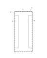
- FIG. 3 is a diagram showing the first surface formed in the process shown in FIG.
- FIG. 4 is a diagram for explaining the manufacturing process of the optical filter, showing the process of forming a film on the second surface of the substrate.
- FIG. 5 is a diagram showing the second surface formed in the process shown in FIG.
- FIG. 6 is a diagram showing an example of a process of forming a film on the first surface of the substrate according to the modification.
- FIG. 7 is a diagram showing an example of a process of forming a film on the second surface of the substrate according to the modification.
- FIG. 1 is a plan view of an optical filter according to one embodiment of the invention.
- FIG. 2 is a diagram for explaining the manufacturing process of the optical filter, showing the process of forming a film on the
- FIG. 8 is a diagram showing another example of the process of forming a film on the second surface of the substrate according to the modification.
- FIG. 9 is a cross-sectional view showing an example of an optical product with an optical filter.
- FIG. 10 is an enlarged view of part A in FIG.
- FIG. 11 is a diagram showing an example of another optical product.
- FIG. 1 is a plan view of the optical filter 1, showing the optical filter 1 viewed in the thickness direction of the substrate 10 (hereinafter also simply referred to as "thickness direction").
- the optical filter 1 has at least a first optical film 11 and a second optical film 13 on the entire surface including the edge (outer edge) of the substrate 10 when viewed in the thickness direction of the substrate 10 . Either one is formed.
- the first optical film 11 and the second optical film 13 are ultraviolet reflecting films or ultraviolet absorbing films, that is, films having an ultraviolet shielding function is shown.
- the first and second optical films of the present invention are not limited to ultraviolet shielding films.
- the first and second optical films may be, for example, a film having a visible light shielding function such as a visible light reflecting film or a visible light absorbing film, or a film having an infrared light shielding function such as an infrared reflecting film or an infrared absorbing film. or a film having an electromagnetic wave shielding effect or a heater function, such as a transparent conductive film.
- the substrate 10 in the optical filter 1 has a first surface 10A (principal surface) and a second surface 10B (back surface) opposite to the first surface 10A in the thickness direction, and is rectangular in plan view in the thickness direction. It is a rectangular parallelepiped flat plate having a shape.
- the “thickness direction (of the substrate)” means a direction that intersects the surface on which a film is formed and that is along any normal direction of the surface on which the film is formed.
- the substrate 10 may have a single-layer structure or a multi-layer structure.
- the material of the substrate is not particularly limited, and may be either an organic material or an inorganic material as long as it is a transparent material that transmits visible light. Also, a plurality of different materials may be used in combination.
- glass and crystalline materials are preferable.
- glass include soda lime glass, borosilicate glass, alkali-free glass, quartz glass, and aluminosilicate glass.
- alkali metal ions with a small ionic radius e.g., Li ions, Na ions
- alkali ions with a larger ionic radius e.g., Li ions are Na ions or K ions, and Na ions are K ions.
- Crystal materials include birefringent crystals such as quartz, lithium niobate, and sapphire.
- transparent resin materials examples include acrylic, polyethylene terephthalate, and polycarbonate.
- the thickness of the substrate is preferably 0.1 mm or more and 5 mm or less, more preferably 2 mm or more and 4 mm or less, from the viewpoints of reducing warping when forming a dielectric multilayer film, reducing the height of optical elements, and suppressing cracking.
- FIGS. 2 and 4 are diagrams for explaining the manufacturing process of the optical filter 1.
- FIG. 2 shows the process of forming a film on the first surface 10A of the substrate 10
- FIG. 4 shows the second surface 10B of the substrate 10.
- 3 and 5 show the first surface 10A deposited in the process shown in FIG. 2 and the second surface 10B deposited in the process shown in FIG. 4, respectively.
- the substrate 10 is prepared.
- the substrate 10 has a flat plate shape (rectangular parallelepiped shape), but the shape of the substrate is not limited to a flat plate shape, and may be a block shape or a film shape. Further, the shape of the substrate when viewed from above in the thickness direction may be a disc shape or the like. Furthermore, the two opposing surfaces of the substrate may not be parallel to each other, and at least one of the surfaces may be curved.
- Films are formed on both surfaces (first surface 10A and second surface 10B) of the prepared substrate 10 by a deposition method such as vacuum deposition or sputtering.
- a deposition method such as vacuum deposition or sputtering.
- FIG. 2 while a portion of the outer periphery of the substrate 10 is supported by a rectangular parallelepiped first jig 31, a well-known film formation source 20 arranged below the substrate 10 is applied to the upper first film.
- a film forming material is deposited on the first surface 10A to form the first optical film 11 on the first surface 10A of the substrate 10 .
- a pair of first jigs 31 are arranged along the long sides of the substrate 10 .
- the portion of the first surface 10A supported by the first jig 31 is, as shown in FIG. 3, the exposed portion 12 where the first optical film 11 is not formed.
- the first optical film 11 formed on the first surface 10A has an H shape as shown in FIG.
- the substrate 10 is turned upside down, and as shown in FIG. 4, film formation is performed while a second jig 32 having a rectangular parallelepiped shape supports a part of the outer periphery of the substrate 10 that is different from the part described above.
- a deposition material is deposited from the source 20 onto the upper second surface 10B to form the second optical film 13 on the second surface 10B of the substrate 10 .
- a pair of second jigs 32 are arranged along the short sides of the substrate 10 .
- the portion of the second surface 10B supported by the second jig 32 is, as shown in FIG. 5, an exposed portion 14 where the second optical film 13 is not formed.
- the second optical film 13 formed on the second surface 10B has a rectangular shape as shown in FIG.
- the second optical film 13 is formed at least on a portion 15 corresponding to the exposed portion 12 on the second surface 10B when viewed from above in the thickness direction.
- the optical filter 1 manufactured as described above includes a substrate 10 having a first surface 10A and a second surface 10B opposite to the first surface 10A in the thickness direction, and a second surface 10B formed on the first surface 10A. 1 optical film 11 and a second optical film 13 formed on the second surface 10B.
- the first surface 10A has an exposed portion 12 where the first optical film 11 is not formed.
- the second optical film 13 is formed at least on a portion 15 corresponding to the exposed portion 12 on the second surface 10B when viewed from above in the thickness direction of the substrate 10 .
- the shape of the first optical film 11 is different from the shape of the first surface 10A
- the shape of the second optical film 13 is different from the shape of the second surface 10B.
- the shape of the first optical film 11 is different from the shape of the second optical film 13 .
- the shape of the first optical film 11 and the second optical film 13 superimposed is at least one of the shape of the first surface 10A and the shape of the second surface 10B. matches.
- the light incident on the optical filter 1 is blocked by either the first optical film 11 or the second optical film 13 . Therefore, when the optical filter 1 is attached to the housing of the optical product via an adhesive, the adhesive provided at the end of the optical filter 1 is not exposed to ultraviolet rays. Therefore, since it is not necessary to apply the black ceramic to the outer peripheral portion of the substrate 10 for protecting the adhesive, high-temperature firing accompanying the application of the black ceramic is not performed, and warping of the substrate due to high temperature is prevented. In addition, since the film is formed by the deposit-up method, the surface of the substrate or the film is not contaminated during film formation. Furthermore, since there is no need to cut the substrate after film formation, cutting does not affect the film.
- the shapes of the first and second optical films formed on the substrate 10 are not limited to the shapes shown in FIGS.
- the shape of the first and second optical films can be changed by changing the shape and support location of the jig that supports the substrate 10 .
- FIG. 6 is a view showing an example of a process of forming a film on the first surface 10A of the substrate 10 according to the modification
- FIG. 7 is a process of forming a film on the second surface 10B of the substrate 10 according to the modification. It is a figure which shows an example.
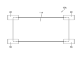
- FIG. 8 is a diagram showing another example of the process of forming a film on the second surface 10B of the substrate 10 according to the modification. 6 to 8 are diagrams of the substrate 10 viewed from below (the side where the film formation source 20 is arranged).
- the first optical film 11A is formed on the first surface 10A while the four corners (part of the outer periphery) of the substrate 10 are supported by the rectangular parallelepiped third jigs 33, respectively.
- the portion of the first surface 10A supported by the third jig 33 is an exposed portion where the first optical film 11A is not formed.
- the first optical film 11A formed on the first surface 10A has an X shape as shown in FIG.
- the substrate 10 After forming the first optical film 11A on the first surface 10A as shown in FIG. 6, the substrate 10 is turned over and the second optical film 13A is formed on the second surface 10B as shown in FIG.
- the second optical film 13A is formed on the second surface 10B while the long sides of the substrate 10 are supported by the rectangular parallelepiped fourth jigs 34, respectively.
- a portion of the second surface 10B supported by the fourth jig 34 is an exposed portion where the second optical film 13A is not formed.
- the second optical film 13A formed on the second surface 10B has an H shape as shown in FIG.
- the second optical film 13A is formed at least at a portion 15-1 corresponding to the exposed portion of the first surface 10A on the second surface 10B when viewed from above in the thickness direction of the substrate 10. As shown in FIG.
- An optical film 13B may be formed.
- the second optical film 13B is formed on the second surface 10B while the short sides of the substrate 10 are supported by fifth rectangular parallelepiped jigs 35, respectively. A portion of the second surface 10B supported by the fifth jig 35 is an exposed portion where the second optical film 13B is not formed.
- the second optical film 13B formed on the second surface 10B has an H shape as shown in FIG.
- the second optical film 13B is formed at least at a portion 15-2 on the second surface 10B corresponding to the exposed portion on the first surface 10A when viewed from above in the thickness direction of the substrate 10. As shown in FIG.
- the incident light is either the first optical film 11A or the second optical films 13A and 13B. is shielded by
- FIG. 9 is a cross-sectional view of an optical product 40 having the optical filter 1
- FIG. 10 is an enlarged view of part A of FIG.
- the optical product 40 includes a box-shaped housing 41 with an open top, a sensor-mounted substrate 42 mounted on the bottom of the housing 41, and the housing 41. and an optical filter 1 placed in the aperture.
- the sensor is, for example, an optical sensor that detects infrared rays or visible rays.
- the optical product 40 is, for example, a LiDAR (Light Detection And Ranging), an image sensor module, or an in-vehicle camera.
- the first optical film 11 is formed on the side of the substrate 10 exposed to the outside, and the second optical film 13 is formed on the side facing the housing 41. .
- the optical filter 1 is adhered to the housing 41 by an adhesive 43 such as a polyurethane adhesive, which is placed on the second optical film 13 .
- the first optical film 11 is not formed on the edge of the substrate 10, but the second optical film 13 is formed on the edge of the substrate 10, so that the second optical film 13 shields the ultraviolet rays. , the adhesive 43 is protected.
- the optical product 40 may also include a functional layer 44 such as a light shielding film between the second optical film 13 and the adhesive 43, as shown in FIG. Further, the optical product 40 has functional layers such as a water-repellent layer, an antistatic layer, an antifogging layer, and a low-reflection layer on the outside of the first optical film 11 (the surface opposite to the surface on which the substrate 10 is provided). You may prepare. Note that the functional layer may be provided between the first optical film 11 or the second optical film 13 and the substrate 10 . Also, the optical product 40 may include a modified first optical film 11A and second optical films 13A and 13B instead of the first optical film 11 and the second optical film 13 .
- the present invention is not limited to the above-described embodiments, and can be modified, improved, etc. as appropriate.
- the material, shape, size, numerical value, form, number, location, etc. of each component in the above-described embodiment are arbitrary and not limited as long as the present invention can be achieved.
- the shape of the first optical film is different from the shape of the first surface
- the shape of the second optical film is different from the shape of the second surface
- the shape of the first optical film is different from the shape of the second optical film
- a shape obtained by overlapping the first optical film and the second optical film coincides with at least one of the shape of the first surface and the shape of the second surface.
- the substrate is a flat plate having a rectangular shape in plan view in the thickness direction, the first surface has an exposed portion (12) where the first optical film is not formed on each long side of the rectangle;
- the optical filter according to any one of [1] to [3] above, wherein the substrate is made of glass.
- the optical filter according to any one of [1] to [3] above, wherein the substrate is made of a crystal material.
- the optical filter according to any one of [1] to [3] above, wherein the substrate is made of a transparent resin material.
- An optical product comprising the optical filter according to any one of [1] to [8] above.
- the substrate is prevented from warping, and the functional film is formed up to the edge of the substrate.
- the optical product of the present invention includes this optical filter. It is useful for applications such as modules and information acquisition devices such as in-vehicle cameras.
Landscapes
- Physics & Mathematics (AREA)
- General Physics & Mathematics (AREA)
- Optics & Photonics (AREA)
- Optical Filters (AREA)
Priority Applications (2)
| Application Number | Priority Date | Filing Date | Title |
|---|---|---|---|
| JP2023552799A JP7800554B2 (ja) | 2021-10-06 | 2022-09-22 | 光学フィルタ及び光学製品 |
| CN202280066876.9A CN118056143A (zh) | 2021-10-06 | 2022-09-22 | 滤光器及光学制品 |
Applications Claiming Priority (2)
| Application Number | Priority Date | Filing Date | Title |
|---|---|---|---|
| JP2021-165062 | 2021-10-06 | ||
| JP2021165062 | 2021-10-06 |
Publications (1)
| Publication Number | Publication Date |
|---|---|
| WO2023058472A1 true WO2023058472A1 (ja) | 2023-04-13 |
Family
ID=85804209
Family Applications (1)
| Application Number | Title | Priority Date | Filing Date |
|---|---|---|---|
| PCT/JP2022/035538 Ceased WO2023058472A1 (ja) | 2021-10-06 | 2022-09-22 | 光学フィルタ及び光学製品 |
Country Status (3)
| Country | Link |
|---|---|
| JP (1) | JP7800554B2 (https=) |
| CN (1) | CN118056143A (https=) |
| WO (1) | WO2023058472A1 (https=) |
Citations (4)
| Publication number | Priority date | Publication date | Assignee | Title |
|---|---|---|---|---|
| JP2004295015A (ja) * | 2003-03-28 | 2004-10-21 | Nidec Copal Corp | Ndフィルタ及びその製造方法 |
| JP2013167701A (ja) * | 2012-02-14 | 2013-08-29 | Seiko Epson Corp | 光学フィルターデバイス、及び光学フィルターデバイスの製造方法 |
| JP2019139165A (ja) * | 2018-02-14 | 2019-08-22 | キヤノン電子株式会社 | Ndフィルタ、光源角度測定装置並びに人工衛星 |
| JP2020056874A (ja) * | 2018-10-01 | 2020-04-09 | キヤノン電子株式会社 | 光学フィルタ及び光学装置 |
-
2022
- 2022-09-22 JP JP2023552799A patent/JP7800554B2/ja active Active
- 2022-09-22 WO PCT/JP2022/035538 patent/WO2023058472A1/ja not_active Ceased
- 2022-09-22 CN CN202280066876.9A patent/CN118056143A/zh active Pending
Patent Citations (4)
| Publication number | Priority date | Publication date | Assignee | Title |
|---|---|---|---|---|
| JP2004295015A (ja) * | 2003-03-28 | 2004-10-21 | Nidec Copal Corp | Ndフィルタ及びその製造方法 |
| JP2013167701A (ja) * | 2012-02-14 | 2013-08-29 | Seiko Epson Corp | 光学フィルターデバイス、及び光学フィルターデバイスの製造方法 |
| JP2019139165A (ja) * | 2018-02-14 | 2019-08-22 | キヤノン電子株式会社 | Ndフィルタ、光源角度測定装置並びに人工衛星 |
| JP2020056874A (ja) * | 2018-10-01 | 2020-04-09 | キヤノン電子株式会社 | 光学フィルタ及び光学装置 |
Also Published As
| Publication number | Publication date |
|---|---|
| JP7800554B2 (ja) | 2026-01-16 |
| CN118056143A (zh) | 2024-05-17 |
| JPWO2023058472A1 (https=) | 2023-04-13 |
Similar Documents
| Publication | Publication Date | Title |
|---|---|---|
| CN110133788B (zh) | 偏光片、显示面板及显示装置 | |
| JP6034785B2 (ja) | 光学部材 | |
| US8233219B2 (en) | Optical multilayer thin-film filters and methods for manufacturing same | |
| US10792886B2 (en) | Decorative film and electronic device including the same | |
| KR101650065B1 (ko) | 광학 필터 부재 및 이것을 구비한 촬상장치 | |
| KR101908541B1 (ko) | 투명 기판 | |
| JP2021033039A (ja) | 液晶装置、液晶装置の製造方法、および電子機器 | |
| CN102305937B (zh) | 闪烁体封装结构 | |
| CN1270195C (zh) | 液晶板用防尘基片及其制造方法 | |
| US20130286480A1 (en) | Retardation plate and electronic apparatus | |
| KR102502417B1 (ko) | 영상 표시 장치, 와이어 그리드 편광판 및 그의 제조 방법, 와이어 그리드 편광판의 관측 방법, 그리고 와이어 그리드 편광판의 편광축 방향의 추정 방법 | |
| KR20150141145A (ko) | 광학 소자 | |
| US20190196265A1 (en) | Display device | |
| WO2005059610A1 (ja) | 光学フィルタ | |
| JP7800554B2 (ja) | 光学フィルタ及び光学製品 | |
| JP2004126530A (ja) | 反射防止膜付き基板の製造方法 | |
| CN110506307B (zh) | 图像显示装置的制造方法及通过该制造方法所得的图像显示装置 | |
| JP2010091828A (ja) | 液晶光学素子とその製造方法 | |
| KR102856597B1 (ko) | 플렉시블 몰드의 제조 방법, 플렉시블 몰드용의 기재, 및 광학 부품의 제조 방법 | |
| CN105487305A (zh) | 一种lcd红外光阀器件及其制作方法 | |
| CN103376481A (zh) | 光学镜片及其制作方法 | |
| EP3373308B1 (en) | Radiation image conversion panel, method for producing radiation image conversion panel, radiation image sensor, and method for producing radiation image sensor | |
| KR102066411B1 (ko) | 디스플레이 패널 | |
| US20130020461A1 (en) | Rearview mirror with monitor | |
| JP2008070828A (ja) | 赤外線遮蔽フィルタ |
Legal Events
| Date | Code | Title | Description |
|---|---|---|---|
| 121 | Ep: the epo has been informed by wipo that ep was designated in this application |
Ref document number: 22878343 Country of ref document: EP Kind code of ref document: A1 |
|
| WWE | Wipo information: entry into national phase |
Ref document number: 2023552799 Country of ref document: JP |
|
| WWE | Wipo information: entry into national phase |
Ref document number: 202280066876.9 Country of ref document: CN |
|
| NENP | Non-entry into the national phase |
Ref country code: DE |
|
| 122 | Ep: pct application non-entry in european phase |
Ref document number: 22878343 Country of ref document: EP Kind code of ref document: A1 |