WO2023058472A1 - 光学フィルタ及び光学製品 - Google Patents
光学フィルタ及び光学製品 Download PDFInfo
- Publication number
- WO2023058472A1 WO2023058472A1 PCT/JP2022/035538 JP2022035538W WO2023058472A1 WO 2023058472 A1 WO2023058472 A1 WO 2023058472A1 JP 2022035538 W JP2022035538 W JP 2022035538W WO 2023058472 A1 WO2023058472 A1 WO 2023058472A1
- Authority
- WO
- WIPO (PCT)
- Prior art keywords
- optical
- film
- substrate
- optical film
- shape
- Prior art date
Links
- 230000003287 optical effect Effects 0.000 title claims abstract description 87
- 239000012788 optical film Substances 0.000 claims abstract description 120
- 239000000758 substrate Substances 0.000 claims abstract description 88
- 239000010408 film Substances 0.000 claims abstract description 63
- 239000000463 material Substances 0.000 claims description 16
- 239000000853 adhesive Substances 0.000 claims description 13
- 230000001070 adhesive effect Effects 0.000 claims description 13
- 239000011521 glass Substances 0.000 claims description 11
- 239000002346 layers by function Substances 0.000 claims description 7
- 239000011347 resin Substances 0.000 claims description 4
- 229920005989 resin Polymers 0.000 claims description 4
- 239000002178 crystalline material Substances 0.000 claims description 3
- 238000000034 method Methods 0.000 description 17
- 238000010586 diagram Methods 0.000 description 11
- 238000000151 deposition Methods 0.000 description 10
- 230000008021 deposition Effects 0.000 description 9
- 230000004048 modification Effects 0.000 description 9
- 238000012986 modification Methods 0.000 description 9
- 230000015572 biosynthetic process Effects 0.000 description 8
- 238000004519 manufacturing process Methods 0.000 description 6
- 239000000919 ceramic Substances 0.000 description 5
- 239000010410 layer Substances 0.000 description 5
- 239000013078 crystal Substances 0.000 description 3
- 238000005520 cutting process Methods 0.000 description 3
- 150000002500 ions Chemical class 0.000 description 3
- 229910001415 sodium ion Inorganic materials 0.000 description 3
- VYPSYNLAJGMNEJ-UHFFFAOYSA-N Silicium dioxide Chemical compound O=[Si]=O VYPSYNLAJGMNEJ-UHFFFAOYSA-N 0.000 description 2
- 229910010272 inorganic material Inorganic materials 0.000 description 2
- 239000011147 inorganic material Substances 0.000 description 2
- 229910001416 lithium ion Inorganic materials 0.000 description 2
- 230000002093 peripheral effect Effects 0.000 description 2
- -1 that is Substances 0.000 description 2
- NIXOWILDQLNWCW-UHFFFAOYSA-N acrylic acid group Chemical group C(C=C)(=O)O NIXOWILDQLNWCW-UHFFFAOYSA-N 0.000 description 1
- 239000003513 alkali Substances 0.000 description 1
- 229910001413 alkali metal ion Inorganic materials 0.000 description 1
- 239000005354 aluminosilicate glass Substances 0.000 description 1
- 239000005388 borosilicate glass Substances 0.000 description 1
- 239000006059 cover glass Substances 0.000 description 1
- 238000005336 cracking Methods 0.000 description 1
- 238000001514 detection method Methods 0.000 description 1
- 230000002542 deteriorative effect Effects 0.000 description 1
- 230000000694 effects Effects 0.000 description 1
- 238000010304 firing Methods 0.000 description 1
- GQYHUHYESMUTHG-UHFFFAOYSA-N lithium niobate Chemical compound [Li+].[O-][Nb](=O)=O GQYHUHYESMUTHG-UHFFFAOYSA-N 0.000 description 1
- 239000000203 mixture Substances 0.000 description 1
- 239000011368 organic material Substances 0.000 description 1
- 239000002245 particle Substances 0.000 description 1
- 229920000515 polycarbonate Polymers 0.000 description 1
- 239000004417 polycarbonate Substances 0.000 description 1
- 229920000139 polyethylene terephthalate Polymers 0.000 description 1
- 239000005020 polyethylene terephthalate Substances 0.000 description 1
- 229920002635 polyurethane Polymers 0.000 description 1
- 239000004814 polyurethane Substances 0.000 description 1
- 239000010453 quartz Substances 0.000 description 1
- 239000005871 repellent Substances 0.000 description 1
- 229910052594 sapphire Inorganic materials 0.000 description 1
- 239000010980 sapphire Substances 0.000 description 1
- 239000002356 single layer Substances 0.000 description 1
- 239000005361 soda-lime glass Substances 0.000 description 1
- 238000004544 sputter deposition Methods 0.000 description 1
- 239000012780 transparent material Substances 0.000 description 1
- 238000001771 vacuum deposition Methods 0.000 description 1
Images


Classifications
-
- B—PERFORMING OPERATIONS; TRANSPORTING
- B32—LAYERED PRODUCTS
- B32B—LAYERED PRODUCTS, i.e. PRODUCTS BUILT-UP OF STRATA OF FLAT OR NON-FLAT, e.g. CELLULAR OR HONEYCOMB, FORM
- B32B7/00—Layered products characterised by the relation between layers; Layered products characterised by the relative orientation of features between layers, or by the relative values of a measurable parameter between layers, i.e. products comprising layers having different physical, chemical or physicochemical properties; Layered products characterised by the interconnection of layers
- B32B7/02—Physical, chemical or physicochemical properties
- B32B7/023—Optical properties
-
- G—PHYSICS
- G02—OPTICS
- G02B—OPTICAL ELEMENTS, SYSTEMS OR APPARATUS
- G02B5/00—Optical elements other than lenses
- G02B5/20—Filters
- G02B5/22—Absorbing filters
-
- G—PHYSICS
- G02—OPTICS
- G02B—OPTICAL ELEMENTS, SYSTEMS OR APPARATUS
- G02B5/00—Optical elements other than lenses
- G02B5/20—Filters
- G02B5/26—Reflecting filters
-
- G—PHYSICS
- G02—OPTICS
- G02B—OPTICAL ELEMENTS, SYSTEMS OR APPARATUS
- G02B5/00—Optical elements other than lenses
- G02B5/20—Filters
- G02B5/28—Interference filters
Definitions
- the present invention relates to optical filters and optical products.
- a glass substrate with an antireflection film formed on its surface is sometimes used as a cover glass for sensors such as image sensors, and is adhered to the housing via an adhesive provided on the outer periphery.
- a material prepared by adjusting a composition containing black ceramic particles (hereinafter referred to as black ceramic) is applied to the outer peripheral portion of the glass substrate in order to prevent the adhesive from deteriorating due to ultraviolet rays.
- black ceramic when applied to a glass substrate, it is fired at a high temperature of, for example, about 600 degrees, which may warp the substrate and make it difficult to adhere to the housing.
- the antireflection film As a countermeasure, it is conceivable to give the antireflection film a UV shielding function.
- a deposition source is placed below the substrate and a deposition material is deposited upward from the deposition source, it is necessary to hold the edge of the substrate. A film cannot be formed on the portion where the ultraviolet ray shielding function cannot be imparted to the portion.
- a deposition source is arranged above the substrate and the deposition material is deposited downward from the deposition source, for example, the deposition material adheres to the inner wall of the chamber of the deposition apparatus. The film material may flake off and contaminate the substrate surface or film surface.
- the present invention has been made in view of the circumstances described above, and its object is to provide an optical filter and an optical product in which a functional film is formed up to the edge of a substrate without impairing the quality of the substrate or the functional film. to do.
- an optical filter and an optical product according to the present invention are characterized by the following (1) to (9).
- a substrate having a first surface and a second surface opposite to the first surface in the thickness direction; a first optical film formed on the first surface; a second optical film formed on the second surface; The first surface has an exposed portion where the first optical film is not formed,
- the shape of the first optical film is different from the shape of the first surface
- the shape of the second optical film is different from the shape of the second surface
- the shape of the first optical film is different from the shape of the second optical film
- a shape obtained by overlapping the first optical film and the second optical film coincides with at least one of the shape of the first surface and the shape of the second surface.
- an optical filter and an optical product in which the functional film is formed up to the edge of the substrate without impairing the quality of the substrate or the functional film.
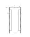
- FIG. 1 is a plan view of an optical filter according to one embodiment of the invention.
- FIG. 2 is a diagram for explaining the manufacturing process of the optical filter, showing the process of forming a film on the first surface of the substrate.
- FIG. 3 is a diagram showing the first surface formed in the process shown in FIG.
- FIG. 4 is a diagram for explaining the manufacturing process of the optical filter, showing the process of forming a film on the second surface of the substrate.
- FIG. 5 is a diagram showing the second surface formed in the process shown in FIG.
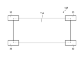
- FIG. 6 is a diagram showing an example of a process of forming a film on the first surface of the substrate according to the modification.
- FIG. 7 is a diagram showing an example of a process of forming a film on the second surface of the substrate according to the modification.
- FIG. 1 is a plan view of an optical filter according to one embodiment of the invention.
- FIG. 2 is a diagram for explaining the manufacturing process of the optical filter, showing the process of forming a film on the
- FIG. 8 is a diagram showing another example of the process of forming a film on the second surface of the substrate according to the modification.
- FIG. 9 is a cross-sectional view showing an example of an optical product with an optical filter.
- FIG. 10 is an enlarged view of part A in FIG.
- FIG. 11 is a diagram showing an example of another optical product.
- FIG. 1 is a plan view of the optical filter 1, showing the optical filter 1 viewed in the thickness direction of the substrate 10 (hereinafter also simply referred to as "thickness direction").
- the optical filter 1 has at least a first optical film 11 and a second optical film 13 on the entire surface including the edge (outer edge) of the substrate 10 when viewed in the thickness direction of the substrate 10 . Either one is formed.
- the first optical film 11 and the second optical film 13 are ultraviolet reflecting films or ultraviolet absorbing films, that is, films having an ultraviolet shielding function is shown.
- the first and second optical films of the present invention are not limited to ultraviolet shielding films.
- the first and second optical films may be, for example, a film having a visible light shielding function such as a visible light reflecting film or a visible light absorbing film, or a film having an infrared light shielding function such as an infrared reflecting film or an infrared absorbing film. or a film having an electromagnetic wave shielding effect or a heater function, such as a transparent conductive film.
- the substrate 10 in the optical filter 1 has a first surface 10A (principal surface) and a second surface 10B (back surface) opposite to the first surface 10A in the thickness direction, and is rectangular in plan view in the thickness direction. It is a rectangular parallelepiped flat plate having a shape.
- the “thickness direction (of the substrate)” means a direction that intersects the surface on which a film is formed and that is along any normal direction of the surface on which the film is formed.
- the substrate 10 may have a single-layer structure or a multi-layer structure.
- the material of the substrate is not particularly limited, and may be either an organic material or an inorganic material as long as it is a transparent material that transmits visible light. Also, a plurality of different materials may be used in combination.
- glass and crystalline materials are preferable.
- glass include soda lime glass, borosilicate glass, alkali-free glass, quartz glass, and aluminosilicate glass.
- alkali metal ions with a small ionic radius e.g., Li ions, Na ions
- alkali ions with a larger ionic radius e.g., Li ions are Na ions or K ions, and Na ions are K ions.
- Crystal materials include birefringent crystals such as quartz, lithium niobate, and sapphire.
- transparent resin materials examples include acrylic, polyethylene terephthalate, and polycarbonate.
- the thickness of the substrate is preferably 0.1 mm or more and 5 mm or less, more preferably 2 mm or more and 4 mm or less, from the viewpoints of reducing warping when forming a dielectric multilayer film, reducing the height of optical elements, and suppressing cracking.
- FIGS. 2 and 4 are diagrams for explaining the manufacturing process of the optical filter 1.
- FIG. 2 shows the process of forming a film on the first surface 10A of the substrate 10
- FIG. 4 shows the second surface 10B of the substrate 10.
- 3 and 5 show the first surface 10A deposited in the process shown in FIG. 2 and the second surface 10B deposited in the process shown in FIG. 4, respectively.
- the substrate 10 is prepared.
- the substrate 10 has a flat plate shape (rectangular parallelepiped shape), but the shape of the substrate is not limited to a flat plate shape, and may be a block shape or a film shape. Further, the shape of the substrate when viewed from above in the thickness direction may be a disc shape or the like. Furthermore, the two opposing surfaces of the substrate may not be parallel to each other, and at least one of the surfaces may be curved.
- Films are formed on both surfaces (first surface 10A and second surface 10B) of the prepared substrate 10 by a deposition method such as vacuum deposition or sputtering.
- a deposition method such as vacuum deposition or sputtering.
- FIG. 2 while a portion of the outer periphery of the substrate 10 is supported by a rectangular parallelepiped first jig 31, a well-known film formation source 20 arranged below the substrate 10 is applied to the upper first film.
- a film forming material is deposited on the first surface 10A to form the first optical film 11 on the first surface 10A of the substrate 10 .
- a pair of first jigs 31 are arranged along the long sides of the substrate 10 .
- the portion of the first surface 10A supported by the first jig 31 is, as shown in FIG. 3, the exposed portion 12 where the first optical film 11 is not formed.
- the first optical film 11 formed on the first surface 10A has an H shape as shown in FIG.
- the substrate 10 is turned upside down, and as shown in FIG. 4, film formation is performed while a second jig 32 having a rectangular parallelepiped shape supports a part of the outer periphery of the substrate 10 that is different from the part described above.
- a deposition material is deposited from the source 20 onto the upper second surface 10B to form the second optical film 13 on the second surface 10B of the substrate 10 .
- a pair of second jigs 32 are arranged along the short sides of the substrate 10 .
- the portion of the second surface 10B supported by the second jig 32 is, as shown in FIG. 5, an exposed portion 14 where the second optical film 13 is not formed.
- the second optical film 13 formed on the second surface 10B has a rectangular shape as shown in FIG.
- the second optical film 13 is formed at least on a portion 15 corresponding to the exposed portion 12 on the second surface 10B when viewed from above in the thickness direction.
- the optical filter 1 manufactured as described above includes a substrate 10 having a first surface 10A and a second surface 10B opposite to the first surface 10A in the thickness direction, and a second surface 10B formed on the first surface 10A. 1 optical film 11 and a second optical film 13 formed on the second surface 10B.
- the first surface 10A has an exposed portion 12 where the first optical film 11 is not formed.
- the second optical film 13 is formed at least on a portion 15 corresponding to the exposed portion 12 on the second surface 10B when viewed from above in the thickness direction of the substrate 10 .
- the shape of the first optical film 11 is different from the shape of the first surface 10A
- the shape of the second optical film 13 is different from the shape of the second surface 10B.
- the shape of the first optical film 11 is different from the shape of the second optical film 13 .
- the shape of the first optical film 11 and the second optical film 13 superimposed is at least one of the shape of the first surface 10A and the shape of the second surface 10B. matches.
- the light incident on the optical filter 1 is blocked by either the first optical film 11 or the second optical film 13 . Therefore, when the optical filter 1 is attached to the housing of the optical product via an adhesive, the adhesive provided at the end of the optical filter 1 is not exposed to ultraviolet rays. Therefore, since it is not necessary to apply the black ceramic to the outer peripheral portion of the substrate 10 for protecting the adhesive, high-temperature firing accompanying the application of the black ceramic is not performed, and warping of the substrate due to high temperature is prevented. In addition, since the film is formed by the deposit-up method, the surface of the substrate or the film is not contaminated during film formation. Furthermore, since there is no need to cut the substrate after film formation, cutting does not affect the film.
- the shapes of the first and second optical films formed on the substrate 10 are not limited to the shapes shown in FIGS.
- the shape of the first and second optical films can be changed by changing the shape and support location of the jig that supports the substrate 10 .
- FIG. 6 is a view showing an example of a process of forming a film on the first surface 10A of the substrate 10 according to the modification
- FIG. 7 is a process of forming a film on the second surface 10B of the substrate 10 according to the modification. It is a figure which shows an example.
- FIG. 8 is a diagram showing another example of the process of forming a film on the second surface 10B of the substrate 10 according to the modification. 6 to 8 are diagrams of the substrate 10 viewed from below (the side where the film formation source 20 is arranged).
- the first optical film 11A is formed on the first surface 10A while the four corners (part of the outer periphery) of the substrate 10 are supported by the rectangular parallelepiped third jigs 33, respectively.
- the portion of the first surface 10A supported by the third jig 33 is an exposed portion where the first optical film 11A is not formed.
- the first optical film 11A formed on the first surface 10A has an X shape as shown in FIG.
- the substrate 10 After forming the first optical film 11A on the first surface 10A as shown in FIG. 6, the substrate 10 is turned over and the second optical film 13A is formed on the second surface 10B as shown in FIG.
- the second optical film 13A is formed on the second surface 10B while the long sides of the substrate 10 are supported by the rectangular parallelepiped fourth jigs 34, respectively.
- a portion of the second surface 10B supported by the fourth jig 34 is an exposed portion where the second optical film 13A is not formed.
- the second optical film 13A formed on the second surface 10B has an H shape as shown in FIG.
- the second optical film 13A is formed at least at a portion 15-1 corresponding to the exposed portion of the first surface 10A on the second surface 10B when viewed from above in the thickness direction of the substrate 10. As shown in FIG.
- An optical film 13B may be formed.
- the second optical film 13B is formed on the second surface 10B while the short sides of the substrate 10 are supported by fifth rectangular parallelepiped jigs 35, respectively. A portion of the second surface 10B supported by the fifth jig 35 is an exposed portion where the second optical film 13B is not formed.
- the second optical film 13B formed on the second surface 10B has an H shape as shown in FIG.
- the second optical film 13B is formed at least at a portion 15-2 on the second surface 10B corresponding to the exposed portion on the first surface 10A when viewed from above in the thickness direction of the substrate 10. As shown in FIG.
- the incident light is either the first optical film 11A or the second optical films 13A and 13B. is shielded by
- FIG. 9 is a cross-sectional view of an optical product 40 having the optical filter 1
- FIG. 10 is an enlarged view of part A of FIG.
- the optical product 40 includes a box-shaped housing 41 with an open top, a sensor-mounted substrate 42 mounted on the bottom of the housing 41, and the housing 41. and an optical filter 1 placed in the aperture.
- the sensor is, for example, an optical sensor that detects infrared rays or visible rays.
- the optical product 40 is, for example, a LiDAR (Light Detection And Ranging), an image sensor module, or an in-vehicle camera.
- the first optical film 11 is formed on the side of the substrate 10 exposed to the outside, and the second optical film 13 is formed on the side facing the housing 41. .
- the optical filter 1 is adhered to the housing 41 by an adhesive 43 such as a polyurethane adhesive, which is placed on the second optical film 13 .
- the first optical film 11 is not formed on the edge of the substrate 10, but the second optical film 13 is formed on the edge of the substrate 10, so that the second optical film 13 shields the ultraviolet rays. , the adhesive 43 is protected.
- the optical product 40 may also include a functional layer 44 such as a light shielding film between the second optical film 13 and the adhesive 43, as shown in FIG. Further, the optical product 40 has functional layers such as a water-repellent layer, an antistatic layer, an antifogging layer, and a low-reflection layer on the outside of the first optical film 11 (the surface opposite to the surface on which the substrate 10 is provided). You may prepare. Note that the functional layer may be provided between the first optical film 11 or the second optical film 13 and the substrate 10 . Also, the optical product 40 may include a modified first optical film 11A and second optical films 13A and 13B instead of the first optical film 11 and the second optical film 13 .
- the present invention is not limited to the above-described embodiments, and can be modified, improved, etc. as appropriate.
- the material, shape, size, numerical value, form, number, location, etc. of each component in the above-described embodiment are arbitrary and not limited as long as the present invention can be achieved.
- the shape of the first optical film is different from the shape of the first surface
- the shape of the second optical film is different from the shape of the second surface
- the shape of the first optical film is different from the shape of the second optical film
- a shape obtained by overlapping the first optical film and the second optical film coincides with at least one of the shape of the first surface and the shape of the second surface.
- the substrate is a flat plate having a rectangular shape in plan view in the thickness direction, the first surface has an exposed portion (12) where the first optical film is not formed on each long side of the rectangle;
- the optical filter according to any one of [1] to [3] above, wherein the substrate is made of glass.
- the optical filter according to any one of [1] to [3] above, wherein the substrate is made of a crystal material.
- the optical filter according to any one of [1] to [3] above, wherein the substrate is made of a transparent resin material.
- An optical product comprising the optical filter according to any one of [1] to [8] above.
- the substrate is prevented from warping, and the functional film is formed up to the edge of the substrate.
- the optical product of the present invention includes this optical filter. It is useful for applications such as modules and information acquisition devices such as in-vehicle cameras.
Landscapes
- Physics & Mathematics (AREA)
- General Physics & Mathematics (AREA)
- Optics & Photonics (AREA)
- Optical Filters (AREA)
Abstract
基板又は機能膜の品質を損なうことなく、基板の端部まで機能膜が形成された、光学フィルタ及び光学製品を提供することを目的とする。光学フィルタは、第1面と、前記第1面と厚み方向で反対側の第2面と、を有する基板と、前記第1面に形成される第1の光学膜と、前記第2面に形成される第2の光学膜と、を備え、前記第1面は、前記第1の光学膜が形成されていない露出部を有し、前記第2の光学膜は、少なくとも、前記厚み方向に平面視して、前記第2面における前記露出部に対応する箇所に形成される。
Description
本発明は、光学フィルタ及び光学製品に関する。
表面に反射防止膜が形成されたガラス基板は、イメージセンサ等のセンサ用カバーガラスとして用いられることがあり、外周部に設けられた接着剤を介して筐体に接着される。このガラス基板の外周部には、接着剤が紫外線により劣化することを防ぐため、黒色のセラミック粒子を含む組成物を調整した材料(以下、黒色セラミックという)が付与されている。
しかしながら、ガラス基板に黒色セラミックを付与する際、例えば約600度の高温で焼成を行うため、基板が反り、筐体への接着が困難な場合がある。
この対策として、反射防止膜に紫外線遮へい機能を持たせることが考えられる。しかし、基板の下方に成膜源を配置して、成膜源から上方に向けて成膜材料を蒸着するデポアップ方式で成膜しようとすると、基板の端部を保持する必要があり、保持される箇所には膜を形成できず、この箇所には紫外線遮へい機能を付与できない。一方、基板の上方に成膜源を配置して、成膜源から下方に向けて成膜材料を蒸着するデポダウン方式で成膜しようとすると、例えば、成膜装置のチャンバ内側壁に付着した成膜材料が剥がれ落ちて、基板表面又は膜表面を汚染する場合がある。
また、大型の基板(大板)に成膜した後に、膜が形成された大板を所定サイズに切断することで、端部まで膜が形成された基板を製造し得る。しかし、成膜後に切断されることによる、膜の品質等への影響が懸念される。
本発明は、上述した事情に鑑みてなされたものであり、その目的は、基板又は機能膜の品質を損なうことなく、基板の端部まで機能膜が形成された、光学フィルタ及び光学製品を提供することにある。
前述した目的を達成するために、本発明に係る光学フィルタ及び光学製品は、下記(1)から(9)を特徴としている。
(1)第1面と、前記第1面と厚み方向で反対側の第2面と、を有する基板と、
前記第1面に形成される第1の光学膜と、
前記第2面に形成される第2の光学膜と、を備え、
前記第1面は、前記第1の光学膜が形成されていない露出部を有し、
前記第2の光学膜は、少なくとも、前記厚み方向に平面視して、前記第2面における前記露出部に対応する箇所に形成される、光学フィルタ。
(2)前記第1の光学膜の形状は、前記第1面の形状とは異なり、
前記第2の光学膜の形状は、前記第2面の形状とは異なり、
前記第1の光学膜の形状は、前記第2の光学膜の形状とは異なり、
前記厚み方向の平面視において、前記第1の光学膜と前記第2の光学膜とを重ね合わせた形状は、前記第1面の形状および前記第2面の形状の少なくともいずれか一方と一致する、上記(1)に記載の光学フィルタ。
(3)前記基板は、ガラスからなる、上記(1)又は(2)に記載の光学フィルタ。
(4)前記基板は、結晶材料からなる、上記(1)又は(2)に記載の光学フィルタ。
(5)前記基板は、透明樹脂材料からなる、上記(1)又は(2)に記載の光学フィルタ。
(6)前記第1の光学膜又は前記第2の光学膜は、紫外線吸収膜又は紫外線反射膜である、上記(1)から(5)のいずれか一に記載の光学フィルタ。
(7)前記第1の光学膜又は前記第2の光学膜の少なくとも一部に機能層を備えた、上記(1)から(6)のいずれか一に記載の光学フィルタ。
(8)上記(1)から(7)のいずれか一に記載の光学フィルタを備えた、光学製品。
(9)前記第1の光学膜又は前記第2の光学膜に、接着剤を備えた、上記(8)に記載の光学製品。
本発明によれば、基板又は機能膜の品質を損なうことなく、基板の端部まで機能膜が形成された、光学フィルタ及び光学製品を提供できる。
以上、本発明について簡潔に説明した。更に、以下に説明される発明を実施するための形態(以下、「実施形態」という。)を添付の図面を参照して通読することにより、本発明の詳細は更に明確化されるであろう。
本発明に関する具体的な実施形態について、各図を参照しながら以下に説明する。
<光学フィルタ>
図1を参照して、本発明の一実施形態に係る光学フィルタ1について説明する。
図1は、光学フィルタ1の平面図であり、基板10の厚み方向(以下、単に「厚み方向」ともいう)に視た光学フィルタ1を示す。図1に示すように、光学フィルタ1は、基板10の厚み方向に視て、基板10の端部(外縁部)を含む全面に、第1の光学膜11及び第2の光学膜13の少なくともいずれか一方が形成されている。本実施形態では、第1の光学膜11及び第2の光学膜13が、紫外線反射膜又は紫外線吸収膜である、すなわち紫外線遮へい機能を有する膜である例を示す。尚、本発明の第1、第2の光学膜は、紫外線遮へい膜に限定されない。第1、第2の光学膜は、例えば、可視光線反射膜又は可視光線吸収膜といった可視光線遮へい機能を有する膜であってもよいし、赤外線反射膜又は赤外線吸収膜といった赤外線遮へい機能を有する膜であってもよいし、透明導電膜といった、電磁波遮蔽効果やヒーター機能を有する膜であってもよい。
<基板>
光学フィルタ1における基板10は、第1面10A(主面)と、第1面10Aと厚み方向で反対側の第2面10B(裏面)と、を有し、厚み方向に平面視して矩形形状を有する、直方体形状の平板である。本開示において、「(基板の)厚み方向」は、成膜される面と交わる方向であって、成膜される面におけるいずれかの法線方向に沿う方向を意味する。
光学フィルタ1における基板10は、第1面10A(主面)と、第1面10Aと厚み方向で反対側の第2面10B(裏面)と、を有し、厚み方向に平面視して矩形形状を有する、直方体形状の平板である。本開示において、「(基板の)厚み方向」は、成膜される面と交わる方向であって、成膜される面におけるいずれかの法線方向に沿う方向を意味する。
基板10は、単層構造であっても、複層構造であってもよい。また基板の材質としては可視光線を透過する透明性材料であれば、有機材料でも無機材料でもよく、特に制限されない。また、異なる複数の材料を複合して用いてもよい。
透明性無機材料としては、ガラスや結晶材料が好ましい。
ガラスとしては、ソーダライムガラス、ホウケイ酸ガラス、無アルカリガラス、石英ガラス、アルミノシリケートガラス等が挙げられる。
ガラスとしては、ガラス転移点以下の温度で、イオン交換により、ガラス板主面に存在するイオン半径が小さいアルカリ金属イオン(例えば、Liイオン、Naイオン)を、イオン半径のより大きいアルカリイオン(例えば、Liイオンに対してはNaイオンまたはKイオンであり、Naイオンに対してはKイオンである。)に交換して得られる化学強化ガラスを使用してもよい。
ガラスとしては、ソーダライムガラス、ホウケイ酸ガラス、無アルカリガラス、石英ガラス、アルミノシリケートガラス等が挙げられる。
ガラスとしては、ガラス転移点以下の温度で、イオン交換により、ガラス板主面に存在するイオン半径が小さいアルカリ金属イオン(例えば、Liイオン、Naイオン)を、イオン半径のより大きいアルカリイオン(例えば、Liイオンに対してはNaイオンまたはKイオンであり、Naイオンに対してはKイオンである。)に交換して得られる化学強化ガラスを使用してもよい。
結晶材料としては、水晶、ニオブ酸リチウム、サファイア等の複屈折性結晶が挙げられる。
透明樹脂材料としては、アクリル、ポリエチレンテレフタレート、ポリカーボネート等が挙げられる。
また基板の厚さは、誘電体多層膜成膜時の反り低減、光学素子低背化、割れ抑制の観点から、0.1mm以上5mm以下が好ましく、より好ましくは2mm以上4mm以下である。
<光学フィルタの製造方法>
図2から図4を参照して、光学フィルタ1の製造方法について説明する。図2及び図4は、光学フィルタ1の製造工程を説明するための図であり、図2は基板10の第1面10Aに成膜する工程を示し、図4は基板10の第2面10Bに成膜する工程を示す。図3及び図5は、図2に示す工程で成膜された第1面10A、及び図4に示す工程で成膜された第2面10Bをそれぞれ示す。
図2から図4を参照して、光学フィルタ1の製造方法について説明する。図2及び図4は、光学フィルタ1の製造工程を説明するための図であり、図2は基板10の第1面10Aに成膜する工程を示し、図4は基板10の第2面10Bに成膜する工程を示す。図3及び図5は、図2に示す工程で成膜された第1面10A、及び図4に示す工程で成膜された第2面10Bをそれぞれ示す。
まず、基板10を準備する。本実施形態では、基板10が平板形状(直方体形状)を有するが、基板の形状は平板形状に限定されず、ブロック状、フィルム状でもよい。また、基板を厚み方向に平面視した形状は円板形状等であってもよい。さらに、基板の対向する二面が、互いに平行でなくてもよく、少なくともいずれか一方の面が湾曲していてもよい。
準備した基板10に対して、真空蒸着やスパッタリング等の成膜方法により、デポアップ方式で両面(第1面10A及び第2面10B)にそれぞれ成膜する。
図2に示すように、基板10の外周部の一部を、直方体形状の第1の治具31で支持しながら、基板10の下方に配置された公知の成膜源20から、上方の第1面10Aに成膜材料を蒸着させ、基板10の第1面10Aに第1の光学膜11を形成する。一対の第1の治具31は、基板10の長辺に沿ってそれぞれ配置される。第1面10Aにおける第1の治具31で支持された箇所は、図3に示すように、第1の光学膜11が形成されていない露出部12とされる。第1面10Aに形成された第1の光学膜11は、図3に示すようにH字状となる。
図2に示すように、基板10の外周部の一部を、直方体形状の第1の治具31で支持しながら、基板10の下方に配置された公知の成膜源20から、上方の第1面10Aに成膜材料を蒸着させ、基板10の第1面10Aに第1の光学膜11を形成する。一対の第1の治具31は、基板10の長辺に沿ってそれぞれ配置される。第1面10Aにおける第1の治具31で支持された箇所は、図3に示すように、第1の光学膜11が形成されていない露出部12とされる。第1面10Aに形成された第1の光学膜11は、図3に示すようにH字状となる。
続いて、基板10を反転させて、図4に示すように、基板10の外周部の上記一部と異なる他の一部を、直方体形状の第2の治具32で支持しながら、成膜源20から、上方の第2面10Bに成膜材料を蒸着させ、基板10の第2面10Bに第2の光学膜13を形成する。一対の第2の治具32は、基板10の短辺に沿ってそれぞれ配置される。第2面10Bにおける第2の治具32で支持された箇所は、図5に示すように、第2の光学膜13が形成されていない露出部14とされる。第2面10Bに形成された第2の光学膜13は、図5に示すように矩形状となる。第2の光学膜13は、厚み方向に平面視して、第2面10Bにおける、露出部12に対応する箇所15に、少なくとも形成される。
上述したように製造された光学フィルタ1は、第1面10Aと、第1面10Aと厚み方向で反対側の第2面10Bと、を有する基板10と、第1面10Aに形成される第1の光学膜11と、第2面10Bに形成される第2の光学膜13と、を備える。第1面10Aは、第1の光学膜11が形成されていない露出部12を有する。第2の光学膜13は、少なくとも、基板10の厚み方向に平面視して、第2面10Bにおける、露出部12に対応する箇所15に形成される。
言い換えれば、厚み方向に視た平面視において、第1の光学膜11の形状は第1面10Aの形状とは異なり、第2の光学膜13の形状は第2面10Bの形状とは異なり、第1の光学膜11の形状は第2の光学膜13の形状とは異なる。また、厚み方向に視た平面視において、第1の光学膜11と第2の光学膜13とを重ね合わせた形状は、第1面10Aの形状および第2面10Bの形状の少なくともいずれか一方と一致する。
このため、光学フィルタ1に入射する光は、第1の光学膜11及び第2の光学膜13のいずれかによって遮へいされる。したがって、光学製品の筐体に、接着剤を介して光学フィルタ1を取り付けた場合、光学フィルタ1の端部に配置された接着剤が紫外線に曝されることがない。よって、接着剤を保護するための黒色セラミックを基板10の外周部に付与する必要がないことから、黒色セラミック付与に伴う高温での焼成が行われず、高温による基板の反り発生が防止される。また、デポアップ方式で成膜するため、成膜時に基板表面又は膜表面が汚染されることがない。さらに、成膜後に基板を切断する必要がないため、切断による膜への影響はない。
<変形例に係る第1の光学膜、第2の光学膜>
基板10に形成される第1及び第2の光学膜の形状は、図1から図5に示す形状に限定されない。基板10を支持する治具の形状及び支持箇所を変更することにより、第1及び第2の光学膜の形状を変更できる。
基板10に形成される第1及び第2の光学膜の形状は、図1から図5に示す形状に限定されない。基板10を支持する治具の形状及び支持箇所を変更することにより、第1及び第2の光学膜の形状を変更できる。
以下、図6から図8を参照して、変形例に係る第1の光学膜11A、第2の光学膜13A、13Bについて説明する。図6は、変形例に係る、基板10の第1面10Aに成膜する工程の一例を示す図であり、図7は、変形例に係る、基板10の第2面10Bに成膜する工程の一例を示す図である。図8は、変形例に係る、基板10の第2面10Bに成膜する工程の他の例を示す図である。図6から図8は、基板10を下方側(成膜源20が配置される側)から視た図である。
図6に示すように、基板10の四隅(外周部の一部)を、直方体形状の第3の治具33でそれぞれ支持しながら、第1面10Aに第1の光学膜11Aを形成する。第1面10Aにおける第3の治具33で支持された箇所は、第1の光学膜11Aが形成されていない露出部とされる。第1面10Aに形成された第1の光学膜11Aは、図6に示すようにX字状となる。
図6に示すように第1面10Aに第1の光学膜11Aを形成した後、基板10を反転させて、図7に示すように第2面10Bに第2の光学膜13Aを形成する。
図7に示すように、基板10の長辺を、直方体形状の第4の治具34でそれぞれ支持しながら、第2面10Bに第2の光学膜13Aを形成する。第2面10Bにおける第4の治具34で支持された箇所は、第2の光学膜13Aが形成されていない露出部とされる。第2面10Bに形成された第2の光学膜13Aは、図7に示すようにH字状となる。第2の光学膜13Aは、少なくとも、基板10の厚み方向に平面視して、第2面10Bにおいて、第1面10Aにおける露出部に対応する箇所15-1に形成される。
他の成膜例として、図6に示すように第1面10Aに第1の光学膜11Aを形成した後、基板10を反転させて、図8に示すように第2面10Bに第2の光学膜13Bを形成してもよい。
図8に示すように、基板10の短辺を、直方体形状の第5の治具35でそれぞれ支持しながら、第2面10Bに第2の光学膜13Bを形成する。第2面10Bにおける第5の治具35で支持された箇所は、第2の光学膜13Bが形成されていない露出部とされる。第2面10Bに形成された第2の光学膜13Bは、図8に示すようにH字状となる。第2の光学膜13Bは、少なくとも、基板10の厚み方向に平面視して、第2面10Bにおいて、第1面10Aにおける露出部に対応する箇所15-2に形成される。
したがって、変形例の第1の光学膜11A及び第2の光学膜13A、13Bを備えた光学フィルタ1によっても、入射する光は第1の光学膜11A及び第2の光学膜13A、13Bのいずれかによって遮へいされる。
<光学製品>
図9から図11を参照して、上述した光学フィルタ1を備えた光学製品40について説明する。
図9から図11を参照して、上述した光学フィルタ1を備えた光学製品40について説明する。
図9は、光学フィルタ1を備えた光学製品40の断面図であり、図10は、図9のA部分を拡大して示す図である。
図9に示すように、光学製品40は、上面が開放された箱型の筐体41と、センサを搭載し、筐体41の底面に配置された、センサ付基板42と、筐体41の開口部に配置された光学フィルタ1と、を備える。尚、センサは図示を省略するが、例えば、赤外線又は可視光線を検出する光センサである。光学製品40は、例えば、LiDAR(Light Detection And Ranging)、イメージセンサモジュール、車載カメラである。
図9に示すように、光学製品40は、上面が開放された箱型の筐体41と、センサを搭載し、筐体41の底面に配置された、センサ付基板42と、筐体41の開口部に配置された光学フィルタ1と、を備える。尚、センサは図示を省略するが、例えば、赤外線又は可視光線を検出する光センサである。光学製品40は、例えば、LiDAR(Light Detection And Ranging)、イメージセンサモジュール、車載カメラである。
図10に示すように、光学フィルタ1は、基板10における、外部に露出する側に第1の光学膜11が形成され、筐体41に面する側に第2の光学膜13が形成される。光学フィルタ1は、第2の光学膜13上に配置された、ポリウレタン接着剤等の接着剤43によって、筐体41に接着される。第1の光学膜11は基板10の端部に形成されていないが、第2の光学膜13が基板10の端部に形成されているため、第2の光学膜13によって紫外線が遮へいされて、接着剤43が保護される。
また、光学製品40は、図11に示すように、第2の光学膜13と接着剤43との間に、遮光膜等の機能層44を備えてもよい。また、光学製品40は、第1の光学膜11の外側(基板10が設けられた面と反対側の面)に撥水層、帯電防止層、防曇層、低反射層等の機能層を備えてもよい。尚、機能層は、第1の光学膜11又は第2の光学膜13と基板10との間に設けられてもよい。また、光学製品40は、第1の光学膜11及び第2の光学膜13に代えて、変形例の第1の光学膜11A及び第2の光学膜13A、13Bを備えてもよい。
尚、本発明は、前述した実施形態に限定されるものではなく、適宜、変形、改良、等が可能である。その他、前述した実施形態における各構成要素の材質、形状、寸法、数値、形態、数、配置箇所、等は本発明を達成できるものであれば任意であり、限定されない。
ここで、上述した本発明の実施形態に係る光学フィルタ及び光学製品の特徴をそれぞれ以下[1]から[10]に簡潔に纏めて列記する。
[1]第1面(10A)と、前記第1面と厚み方向で反対側の第2面(10B)と、を有する基板(10)と、
前記第1面に形成される第1の光学膜(11)と、
前記第2面に形成される第2の光学膜(13)と、を備え、
前記第1面は、前記第1の光学膜が形成されていない露出部(12)を有し、
前記第2の光学膜は、少なくとも、前記厚み方向に平面視して、前記第2面における前記露出部に対応する箇所(15)に形成される、光学フィルタ(1)。
[2]前記第1の光学膜の形状は、前記第1面の形状とは異なり、
前記第2の光学膜の形状は、前記第2面の形状とは異なり、
前記第1の光学膜の形状は、前記第2の光学膜の形状とは異なり、
前記厚み方向の平面視において、前記第1の光学膜と前記第2の光学膜とを重ね合わせた形状は、前記第1面の形状および前記第2面の形状の少なくともいずれか一方と一致する、上記[1]に記載の光学フィルタ。
[3]前記基板は、前記厚み方向の平面視において矩形形状を有する平板であり、
前記第1面は、前記矩形の各長辺において、前記第1の光学膜が形成されていない露出部(12)を有し、
前記第2面は、前記矩形の各短辺において、前記第2の光学膜が形成されていない露出部(14)を有する、上記[2]に記載の光学フィルタ。
[4]前記基板は、ガラスからなる、上記[1]から[3]のいずれか一に記載の光学フィルタ。
[5]前記基板は、結晶材料からなる、上記[1]から[3]のいずれか一に記載の光学フィルタ。
[6]前記基板は、透明樹脂材料からなる、上記[1]から[3]のいずれか一に記載の光学フィルタ。
[7]前記第1の光学膜又は前記第2の光学膜は、紫外線吸収膜又は紫外線反射膜である、上記[1]から[6]のいずれか一に記載の光学フィルタ。
[8]前記第1の光学膜又は前記第2の光学膜の少なくとも一部に機能層を備えた、上記
[1]から[7]のいずれか一に記載の光学フィルタ。
[9]上記[1]から[8]のいずれか一に記載の光学フィルタを備えた、光学製品。
[10]前記第1の光学膜又は前記第2の光学膜に、接着剤を備えた、上記[9]に記載の光学製品。
以上、図面を参照しながら各種の実施の形態について説明したが、本発明はかかる例に限定されないことは言うまでもない。当業者であれば、特許請求の範囲に記載された範疇内において、各種の変更例又は修正例に想到し得ることは明らかであり、それらについても当然に本発明の技術的範囲に属するものと了解される。また、発明の趣旨を逸脱しない範囲において、上記実施の形態における各構成要素を任意に組み合わせてもよい。
なお、本出願は、2021年10月6日出願の日本特許出願(特願2021-165062)に基づくものであり、その内容は本出願の中に参照として援用される。
本発明の光学フィルタは、基板の反りが防止され、かつ、基板の端部まで機能膜が形成され、本発明の光学製品は、この光学フィルタを備えることから、例えば、屋外で使用されるセンサーモジュールや、車載カメラ等の情報取得装置の用途に有用である。
1 光学フィルタ
10 基板
10A 第1面
10B 第2面
11、11A 第1の光学膜
12、14 露出部
13、13A、13B 第2の光学膜
15 第2面における露出部に対応する箇所
20 成膜源
31 第1の治具
32 第2の治具
33 第3の治具
34 第4の治具
35 第5の治具
40 光学製品
41 筐体
42 センサ付基板
43 接着剤
44 機能層
10 基板
10A 第1面
10B 第2面
11、11A 第1の光学膜
12、14 露出部
13、13A、13B 第2の光学膜
15 第2面における露出部に対応する箇所
20 成膜源
31 第1の治具
32 第2の治具
33 第3の治具
34 第4の治具
35 第5の治具
40 光学製品
41 筐体
42 センサ付基板
43 接着剤
44 機能層
Claims (9)
- 第1面と、前記第1面と厚み方向で反対側の第2面と、を有する基板と、
前記第1面に形成される第1の光学膜と、
前記第2面に形成される第2の光学膜と、を備え、
前記第1面は、前記第1の光学膜が形成されていない露出部を有し、
前記第2の光学膜は、少なくとも、前記厚み方向に平面視して、前記第2面における前記露出部に対応する箇所に形成される、光学フィルタ。 - 前記第1の光学膜の形状は、前記第1面の形状とは異なり、
前記第2の光学膜の形状は、前記第2面の形状とは異なり、
前記第1の光学膜の形状は、前記第2の光学膜の形状とは異なり、
前記厚み方向の平面視において、前記第1の光学膜と前記第2の光学膜とを重ね合わせた形状は、前記第1面の形状および前記第2面の形状の少なくともいずれか一方と一致する、請求項1に記載の光学フィルタ。 - 前記基板は、ガラスからなる、請求項1又は2に記載の光学フィルタ。
- 前記基板は、結晶材料からなる、請求項1又は2に記載の光学フィルタ。
- 前記基板は、透明樹脂材料からなる、請求項1又は2に記載の光学フィルタ。
- 前記第1の光学膜又は前記第2の光学膜は、紫外線吸収膜又は紫外線反射膜である、請求項1から5のいずれか一項に記載の光学フィルタ。
- 前記第1の光学膜又は前記第2の光学膜の少なくとも一部に機能層を備えた、請求項1から6のいずれか一項に記載の光学フィルタ。
- 請求項1から7のいずれか一項に記載の光学フィルタを備えた、光学製品。
- 前記第1の光学膜又は前記第2の光学膜に、接着剤を備えた、請求項8に記載の光学製品。
Priority Applications (1)
| Application Number | Priority Date | Filing Date | Title |
|---|---|---|---|
| CN202280066876.9A CN118056143A (zh) | 2021-10-06 | 2022-09-22 | 滤光器及光学制品 |
Applications Claiming Priority (2)
| Application Number | Priority Date | Filing Date | Title |
|---|---|---|---|
| JP2021165062 | 2021-10-06 | ||
| JP2021-165062 | 2021-10-06 |
Publications (1)
| Publication Number | Publication Date |
|---|---|
| WO2023058472A1 true WO2023058472A1 (ja) | 2023-04-13 |
Family
ID=85804209
Family Applications (1)
| Application Number | Title | Priority Date | Filing Date |
|---|---|---|---|
| PCT/JP2022/035538 WO2023058472A1 (ja) | 2021-10-06 | 2022-09-22 | 光学フィルタ及び光学製品 |
Country Status (2)
| Country | Link |
|---|---|
| CN (1) | CN118056143A (ja) |
| WO (1) | WO2023058472A1 (ja) |
Citations (4)
| Publication number | Priority date | Publication date | Assignee | Title |
|---|---|---|---|---|
| JP2004295015A (ja) * | 2003-03-28 | 2004-10-21 | Nidec Copal Corp | Ndフィルタ及びその製造方法 |
| JP2013167701A (ja) * | 2012-02-14 | 2013-08-29 | Seiko Epson Corp | 光学フィルターデバイス、及び光学フィルターデバイスの製造方法 |
| JP2019139165A (ja) * | 2018-02-14 | 2019-08-22 | キヤノン電子株式会社 | Ndフィルタ、光源角度測定装置並びに人工衛星 |
| JP2020056874A (ja) * | 2018-10-01 | 2020-04-09 | キヤノン電子株式会社 | 光学フィルタ及び光学装置 |
-
2022
- 2022-09-22 CN CN202280066876.9A patent/CN118056143A/zh active Pending
- 2022-09-22 WO PCT/JP2022/035538 patent/WO2023058472A1/ja active Application Filing
Patent Citations (4)
| Publication number | Priority date | Publication date | Assignee | Title |
|---|---|---|---|---|
| JP2004295015A (ja) * | 2003-03-28 | 2004-10-21 | Nidec Copal Corp | Ndフィルタ及びその製造方法 |
| JP2013167701A (ja) * | 2012-02-14 | 2013-08-29 | Seiko Epson Corp | 光学フィルターデバイス、及び光学フィルターデバイスの製造方法 |
| JP2019139165A (ja) * | 2018-02-14 | 2019-08-22 | キヤノン電子株式会社 | Ndフィルタ、光源角度測定装置並びに人工衛星 |
| JP2020056874A (ja) * | 2018-10-01 | 2020-04-09 | キヤノン電子株式会社 | 光学フィルタ及び光学装置 |
Also Published As
| Publication number | Publication date |
|---|---|
| CN118056143A (zh) | 2024-05-17 |
Similar Documents
| Publication | Publication Date | Title |
|---|---|---|
| CN110133788B (zh) | 偏光片、显示面板及显示装置 | |
| JP6034785B2 (ja) | 光学部材 | |
| US8233219B2 (en) | Optical multilayer thin-film filters and methods for manufacturing same | |
| US10792886B2 (en) | Decorative film and electronic device including the same | |
| KR101650065B1 (ko) | 광학 필터 부재 및 이것을 구비한 촬상장치 | |
| US20130286480A1 (en) | Retardation plate and electronic apparatus | |
| KR101908541B1 (ko) | 투명 기판 | |
| CN1270195C (zh) | 液晶板用防尘基片及其制造方法 | |
| JP2008070828A (ja) | 赤外線遮蔽フィルタ | |
| CN110506307B (zh) | 图像显示装置的制造方法及通过该制造方法所得的图像显示装置 | |
| KR20150141145A (ko) | 광학 소자 | |
| US20190196265A1 (en) | Display device | |
| WO2023058472A1 (ja) | 光学フィルタ及び光学製品 | |
| WO2005059610A1 (ja) | 光学フィルタ | |
| CN113054138A (zh) | 一种盖板及其制备方法、显示装置 | |
| JP2004126530A (ja) | 反射防止膜付き基板の製造方法 | |
| KR102502417B1 (ko) | 영상 표시 장치, 와이어 그리드 편광판 및 그의 제조 방법, 와이어 그리드 편광판의 관측 방법, 그리고 와이어 그리드 편광판의 편광축 방향의 추정 방법 | |
| EP3373308B1 (en) | Radiation image conversion panel, method for producing radiation image conversion panel, radiation image sensor, and method for producing radiation image sensor | |
| US20130020461A1 (en) | Rearview mirror with monitor | |
| US3709765A (en) | Product and process involving optical thin film filters protected against deterioration from humidity | |
| WO2022127036A1 (zh) | 显示装置及偏光片 | |
| KR20190121128A (ko) | 디스플레이 패널 | |
| KR101791111B1 (ko) | 액정표시장치 및 그 제조 장비 | |
| CN105487305A (zh) | 一种lcd红外光阀器件及其制作方法 | |
| JP2003167327A (ja) | ペリクル |
Legal Events
| Date | Code | Title | Description |
|---|---|---|---|
| 121 | Ep: the epo has been informed by wipo that ep was designated in this application |
Ref document number: 22878343 Country of ref document: EP Kind code of ref document: A1 |
|
| WWE | Wipo information: entry into national phase |
Ref document number: 2023552799 Country of ref document: JP |