WO2023054389A1 - 半導体装置および半導体装置の製造方法 - Google Patents
半導体装置および半導体装置の製造方法 Download PDFInfo
- Publication number
- WO2023054389A1 WO2023054389A1 PCT/JP2022/036006 JP2022036006W WO2023054389A1 WO 2023054389 A1 WO2023054389 A1 WO 2023054389A1 JP 2022036006 W JP2022036006 W JP 2022036006W WO 2023054389 A1 WO2023054389 A1 WO 2023054389A1
- Authority
- WO
- WIPO (PCT)
- Prior art keywords
- resin
- wiring
- layer
- semiconductor device
- sealing
- Prior art date
- Legal status (The legal status is an assumption and is not a legal conclusion. Google has not performed a legal analysis and makes no representation as to the accuracy of the status listed.)
- Ceased
Links
Images









Classifications
-
- H—ELECTRICITY
- H10—SEMICONDUCTOR DEVICES; ELECTRIC SOLID-STATE DEVICES NOT OTHERWISE PROVIDED FOR
- H10P—GENERIC PROCESSES OR APPARATUS FOR THE MANUFACTURE OR TREATMENT OF DEVICES COVERED BY CLASS H10
- H10P52/00—Grinding, lapping or polishing of wafers, substrates or parts of devices
-
- H—ELECTRICITY
- H10—SEMICONDUCTOR DEVICES; ELECTRIC SOLID-STATE DEVICES NOT OTHERWISE PROVIDED FOR
- H10W—GENERIC PACKAGES, INTERCONNECTIONS, CONNECTORS OR OTHER CONSTRUCTIONAL DETAILS OF DEVICES COVERED BY CLASS H10
- H10W70/00—Package substrates; Interposers; Redistribution layers [RDL]
- H10W70/60—Insulating or insulated package substrates; Interposers; Redistribution layers
-
- H—ELECTRICITY
- H10—SEMICONDUCTOR DEVICES; ELECTRIC SOLID-STATE DEVICES NOT OTHERWISE PROVIDED FOR
- H10W—GENERIC PACKAGES, INTERCONNECTIONS, CONNECTORS OR OTHER CONSTRUCTIONAL DETAILS OF DEVICES COVERED BY CLASS H10
- H10W70/00—Package substrates; Interposers; Redistribution layers [RDL]
- H10W70/60—Insulating or insulated package substrates; Interposers; Redistribution layers
- H10W70/62—Insulating or insulated package substrates; Interposers; Redistribution layers characterised by their interconnections
- H10W70/65—Shapes or dispositions of interconnections
-
- H—ELECTRICITY
- H10—SEMICONDUCTOR DEVICES; ELECTRIC SOLID-STATE DEVICES NOT OTHERWISE PROVIDED FOR
- H10W—GENERIC PACKAGES, INTERCONNECTIONS, CONNECTORS OR OTHER CONSTRUCTIONAL DETAILS OF DEVICES COVERED BY CLASS H10
- H10W72/00—Interconnections or connectors in packages
- H10W72/20—Bump connectors, e.g. solder bumps or copper pillars; Dummy bumps; Thermal bumps
-
- H—ELECTRICITY
- H10—SEMICONDUCTOR DEVICES; ELECTRIC SOLID-STATE DEVICES NOT OTHERWISE PROVIDED FOR
- H10W—GENERIC PACKAGES, INTERCONNECTIONS, CONNECTORS OR OTHER CONSTRUCTIONAL DETAILS OF DEVICES COVERED BY CLASS H10
- H10W74/00—Encapsulations, e.g. protective coatings
-
- H—ELECTRICITY
- H10—SEMICONDUCTOR DEVICES; ELECTRIC SOLID-STATE DEVICES NOT OTHERWISE PROVIDED FOR
- H10W—GENERIC PACKAGES, INTERCONNECTIONS, CONNECTORS OR OTHER CONSTRUCTIONAL DETAILS OF DEVICES COVERED BY CLASS H10
- H10W74/00—Encapsulations, e.g. protective coatings
- H10W74/01—Manufacture or treatment
-
- H—ELECTRICITY
- H10—SEMICONDUCTOR DEVICES; ELECTRIC SOLID-STATE DEVICES NOT OTHERWISE PROVIDED FOR
- H10W—GENERIC PACKAGES, INTERCONNECTIONS, CONNECTORS OR OTHER CONSTRUCTIONAL DETAILS OF DEVICES COVERED BY CLASS H10
- H10W74/00—Encapsulations, e.g. protective coatings
- H10W74/01—Manufacture or treatment
- H10W74/014—Manufacture or treatment using batch processing
-
- H—ELECTRICITY
- H10—SEMICONDUCTOR DEVICES; ELECTRIC SOLID-STATE DEVICES NOT OTHERWISE PROVIDED FOR
- H10W—GENERIC PACKAGES, INTERCONNECTIONS, CONNECTORS OR OTHER CONSTRUCTIONAL DETAILS OF DEVICES COVERED BY CLASS H10
- H10W74/00—Encapsulations, e.g. protective coatings
- H10W74/01—Manufacture or treatment
- H10W74/019—Manufacture or treatment using temporary auxiliary substrates
-
- H—ELECTRICITY
- H10—SEMICONDUCTOR DEVICES; ELECTRIC SOLID-STATE DEVICES NOT OTHERWISE PROVIDED FOR
- H10W—GENERIC PACKAGES, INTERCONNECTIONS, CONNECTORS OR OTHER CONSTRUCTIONAL DETAILS OF DEVICES COVERED BY CLASS H10
- H10W74/00—Encapsulations, e.g. protective coatings
- H10W74/10—Encapsulations, e.g. protective coatings characterised by their shape or disposition
- H10W74/131—Encapsulations, e.g. protective coatings characterised by their shape or disposition the semiconductor body being only partially enclosed
- H10W74/141—Encapsulations, e.g. protective coatings characterised by their shape or disposition the semiconductor body being only partially enclosed the encapsulations being on at least the sidewalls of the semiconductor body
-
- H—ELECTRICITY
- H10—SEMICONDUCTOR DEVICES; ELECTRIC SOLID-STATE DEVICES NOT OTHERWISE PROVIDED FOR
- H10W—GENERIC PACKAGES, INTERCONNECTIONS, CONNECTORS OR OTHER CONSTRUCTIONAL DETAILS OF DEVICES COVERED BY CLASS H10
- H10W74/00—Encapsulations, e.g. protective coatings
- H10W74/40—Encapsulations, e.g. protective coatings characterised by their materials
-
- H—ELECTRICITY
- H10—SEMICONDUCTOR DEVICES; ELECTRIC SOLID-STATE DEVICES NOT OTHERWISE PROVIDED FOR
- H10W—GENERIC PACKAGES, INTERCONNECTIONS, CONNECTORS OR OTHER CONSTRUCTIONAL DETAILS OF DEVICES COVERED BY CLASS H10
- H10W90/00—Package configurations
- H10W90/701—Package configurations characterised by the relative positions of pads or connectors relative to package parts
- H10W90/721—Package configurations characterised by the relative positions of pads or connectors relative to package parts of bump connectors
- H10W90/724—Package configurations characterised by the relative positions of pads or connectors relative to package parts of bump connectors between a chip and a stacked insulating package substrate, interposer or RDL
Definitions
- the present disclosure relates to a semiconductor device and a method for manufacturing a semiconductor device.
- a semiconductor device includes a semiconductor element having an element surface, an element back surface opposite to the element surface, and an element side surface connecting the element surface and the element back surface, and facing the element back surface.
- a conductive portion provided at a position and having a wiring portion on which the semiconductor element is mounted; and a sealing resin for sealing the semiconductor element and the conductive portion, wherein the wiring portion faces the back surface of the element.
- a wiring surface and a wiring back surface opposite to the wiring surface; the conductive portion has a terminal portion extending from the wiring back surface in a direction opposite to the semiconductor element; , the element rear surface, the element side surface, and the wiring surface, and the element surface is exposed without being covered with the sealing resin.
- a method for manufacturing a semiconductor device includes: a semiconductor element having an element surface, an element back surface opposite to the element surface, and an element side surface connecting the element surface and the element back surface;
- a method for manufacturing a semiconductor device comprising: a conductive portion including a wiring portion provided at a position facing the semiconductor element and including a wiring portion on which the semiconductor element is mounted; and a sealing resin for sealing the semiconductor element and the conductive portion,
- the wiring portion has a wiring surface facing the element back surface and a wiring back surface opposite to the wiring surface, and the conductive portion extends from the wiring back surface in a direction opposite to the semiconductor element.
- the method for manufacturing the semiconductor device includes covering the element surface, the element back surface, and the element side surface of the semiconductor element, and the wiring surface of the wiring section, and forming a part of the sealing resin. forming a resin layer forming a portion; and grinding the resin layer so that the element surface is exposed from the resin layer.
- the heat dissipation performance of the semiconductor device can be improved.
- FIG. 1 is a perspective view of one embodiment of a semiconductor device.
- 2 is a plan view of the semiconductor device of FIG. 1.
- FIG. 3 is a back view of the semiconductor device of FIG. 1.
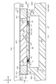
- FIG. 4 is a cross-sectional view of the semiconductor device of FIG. 3 taken along line F4-F4.
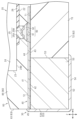
- FIG. 5 is an enlarged view of the conductive portion and its periphery of the semiconductor device of FIG.
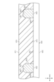
- FIG. 6 is a schematic cross-sectional view showing manufacturing steps of an embodiment of a method for manufacturing a semiconductor device.
- FIG. 7 is a schematic cross-sectional view showing the manufacturing process following FIG.
- FIG. 8 is a schematic cross-sectional view showing a manufacturing process following FIG.
- FIG. 9 is a schematic cross-sectional view showing a manufacturing process following FIG.
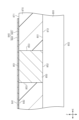
- FIG. 10 is an enlarged view of a portion of FIG. 9.
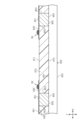
- FIG. FIG. 11 is a schematic cross-sectional view showing the manufacturing process following FIG. 12 is an enlarged view of a portion of FIG. 11.
- FIG. 13A and 13B are schematic cross-sectional views showing the manufacturing process following FIG. 14A and 14B are schematic cross-sectional views showing the manufacturing process following FIG. 15A and 15B are schematic cross-sectional views showing the manufacturing process following FIG.
- FIG. 16 is a schematic cross-sectional view showing the manufacturing process following FIG. 17A and 17B are schematic cross-sectional views showing the manufacturing process following FIG.
- FIG. 18 is a schematic cross-sectional view showing the manufacturing process following FIG.
- FIG. 19 is a schematic cross-sectional view showing the manufacturing process following FIG.
- FIG. 20 is a schematic cross-sectional view showing the manufacturing process following FIG.
- FIG. 21 is an enlarged view of the conductive portion and its surroundings of the semiconductor device of the modification.
- the semiconductor device 10 includes a semiconductor element 20, a conductive portion 30 electrically connected to the semiconductor element 20, and a sealing resin 60 sealing the semiconductor element 20 and the conductive portion 30. and have.
- the semiconductor device 10 is a device surface-mounted on a circuit board (not shown) of various electronic devices. That is, the semiconductor device 10 has a surface mount type package structure.
- the semiconductor device 10 of the present embodiment is a fan-out type semiconductor device in which the terminal portion 50 mounted on the circuit board of the conductive portion 30 is located outside the semiconductor element 20. is.
- the sealing resin 60 constitutes the side surface of the semiconductor device 10.
- the shape of the sealing resin 60 is a substantially rectangular flat plate shape. That is, the shape of the semiconductor device 10 is a substantially rectangular plate shape.
- the thickness direction of the sealing resin 60 is defined as the Z direction.
- the direction along one side of the semiconductor device 10 orthogonal to the Z direction is defined as the X direction
- the direction orthogonal to the X and Z directions is defined as the Y direction.
- the Y direction is also a direction along one side of the semiconductor device 10 when viewed from the Z direction.
- the shape of the sealing resin 60 viewed from the Z direction is square. That is, the shape of the semiconductor device 10 viewed from the Z direction is square.
- the shape of the sealing resin 60 (the shape of the semiconductor device 10) can be arbitrarily changed.
- the shape of the sealing resin 60 (the shape of the semiconductor device 10) viewed from the Z direction may be a rectangle whose X-direction side is longer than its Y-direction side, or whose Y-direction side is longer than the Y-direction side. It may have a rectangular shape longer than the direction side.
- the sealing resin 60 has a resin surface 61 and a resin back surface 62 opposite to the resin surface 61 .
- the sealing resin 60 has four resin side surfaces 63 connecting the resin front surface 61 and the resin back surface 62 in the Z direction. It can be said that the resin surface 61 , the resin back surface 62 , and the four resin side surfaces 63 constitute the outer surface of the semiconductor device 10 .
- the sealing resin 60 has a flat substrate portion 70 and a sealing portion 80 formed on the substrate portion 70 .
- the substrate portion 70 is a support member on which the semiconductor element 20 is mounted and which serves as a base of the semiconductor device 10 .
- the substrate portion 70 is made of an insulating material.
- the substrate portion 70 is made of, for example, black epoxy resin. Any material can be used to form the substrate portion 70 .
- the substrate portion 70 constitutes a portion of the sealing resin 60 closer to the resin back surface 62 .
- the substrate portion 70 has a substrate surface 71 facing the same side as the resin surface 61 and a substrate back surface 72 opposite to the substrate surface 71 .
- the substrate back surface 72 constitutes the resin back surface 62 .
- the substrate section 70 has four substrate side surfaces 73 connecting the substrate front surface 71 and the substrate back surface 72 in the Z direction. The four substrate side surfaces 73 form a portion of the four resin side surfaces 63 that is closer to the resin back surface 62 .
- the sealing portion 80 is a sealing member that seals the semiconductor element 20 .
- the sealing portion 80 is made of an insulating material.
- the sealing portion 80 is made of, for example, black epoxy resin. Any material can be used to form the sealing portion 80 .
- the material forming the substrate portion 70 and the sealing portion 80 may contain, for example, a filler that improves heat dissipation performance.
- both the substrate portion 70 and the sealing portion 80 are made of black epoxy resin.
- the content ratio of the filler contained in the epoxy resin forming the substrate portion 70 and the sealing portion 80 is different from each other. Thereby, an interface is formed at the boundary between the substrate portion 70 and the sealing portion 80 .
- the sealing portion 80 constitutes a portion of the sealing resin 60 near the resin surface 61 .
- the sealing portion 80 has a sealing surface 81 forming the resin surface 61 and a sealing back surface 82 opposite to the sealing surface 81 .
- the sealing surface 81 constitutes the resin surface 61 .
- the sealing back surface 82 is in contact with the substrate front surface 71 of the substrate section 70 . Therefore, the interface between the substrate portion 70 and the sealing portion 80 is formed by the sealing back surface 82 of the sealing portion 80 and the substrate surface 71 of the substrate portion 70 .
- the sealing portion 80 also has four sealing side surfaces 83 connecting the sealing front surface 81 and the sealing back surface 82 in the Z direction. Each sealing side surface 83 is formed so as to be flush with the substrate side surface 73 facing the same side.
- Each encapsulation side 83 is continuous with a substrate side 73 facing the same side.
- the four sealing side surfaces 83 form a portion of the resin side surface 63 that is closer to the resin surface 61 . That is, the resin side surface 63 is composed of the substrate side surface 73 and the sealing side surface 83 .
- the sealing portion 80 has an inwardly recessed stepped portion 84 on each sealing side surface 83 .
- the stepped portion 84 divides the sealing portion 80 into a first sealing portion 85 and a second sealing portion 86 .
- the first sealing portion 85 is a portion of the sealing portion 80 closer to the sealing surface 81
- the second sealing portion 86 is a portion of the sealing portion 80 closer to the sealing back surface 82 .
- the first sealing portion 85 is the portion from the step portion 84 to the sealing surface 81
- the second sealing portion 86 is the portion from the step portion 84 to the sealing back surface 82 .
- the second sealing portion 86 is a portion recessed inward from the first sealing portion 85 .
- the stepped portion 84 is provided at a position overlapping the semiconductor element 20 when viewed from the direction orthogonal to the Z direction. Therefore, both the first sealing portion 85 and the second sealing portion 86 have portions overlapping the semiconductor element 20 when viewed from the direction perpendicular to the Z direction. In particular, the first sealing portion 85 is provided so as to entirely overlap the semiconductor element 20 when viewed from the direction orthogonal to the Z direction.
- the semiconductor element 20 sealed in the sealing portion 80 is an integrated circuit (IC: Integrated Circuit) such as LSI (Large Scale Integration). Also, the semiconductor element 20 may be a discrete semiconductor element such as a voltage control element such as an LDO (Low Drop Out), an amplification element such as an operational amplifier, a diode, and various sensors.
- IC integrated circuit
- LDO Low Drop Out
- amplification element such as an operational amplifier
- diode a diode
- the semiconductor element 20 is formed in a flat plate shape.
- the shape of the semiconductor element 20 viewed from the Z direction is a square.
- the shape of the semiconductor element 20 viewed from the Z direction can be arbitrarily changed.
- the shape of the semiconductor element 20 viewed from the Z direction may be a rectangular shape in which the X direction is the long side direction and the Y direction is the short side direction, or the X direction is the short side direction and the Y direction. may be rectangular in the long side direction.
- the semiconductor element 20 has an element front surface 21 and an element back surface 22 opposite to the element front surface 21 .
- the element surface 21 faces the same side as the resin surface 61 .
- the resin surface 61 faces the same side as the element surface 21 .
- the element back surface 22 faces the same side as the resin back surface 62 . It can also be said that the element back surface 22 faces the substrate front surface 71 of the substrate section 70 .
- the semiconductor element 20 also has four element side surfaces 23 connecting the element front surface 21 and the element back surface 22 in the Z direction.
- the conductive portion 30 has a wiring portion 40 and a terminal portion 50. As shown in FIGS. In this embodiment, the wiring portion 40 and the terminal portion 50 are provided separately.
- the conductive portion 30 is formed by plating.
- the wiring part 40 is a part where the semiconductor element 20 is mounted.
- the wiring portion 40 is formed on the substrate portion 70 .
- the wiring portion 40 is formed on the substrate surface 71 of the substrate portion 70 . Since the substrate surface 71 of the substrate portion 70 is a plane orthogonal to the Z direction, it can be said that the wiring portion 40 extends in a direction orthogonal to the Z direction. In other words, it can be said that the wiring portion 40 is not bent in the Z direction.
- the wiring part 40 is provided at a position facing the element back surface 22 of the semiconductor element 20 .
- a plurality of wiring portions 40 (12 pieces in this embodiment) are provided. As viewed in the Z direction, each wiring portion 40 extends from a position facing the device back surface 22 of the semiconductor device 20 to the outside of the semiconductor device 20 . That is, it can be said that each wiring part 40 has a protruding part protruding from the semiconductor element 20 when viewed in the Z direction.
- each wiring portion 40 has a wiring surface 41 facing the element back surface 22 of the semiconductor element 20 and a wiring back surface 42 opposite to the wiring surface 41 .
- the wiring rear surface 42 is in contact with the substrate front surface 71 of the substrate portion 70 .
- three wiring portions 40 are provided corresponding to each of the four resin side surfaces 63 of the sealing resin 60 . More specifically, when viewed from the Z direction, the plurality of wiring portions 40 provided in the vicinity of the resin side surface 63 extending in the Y direction of the sealing resin 60 among the plurality of wiring portions 40 are aligned in the X direction. They are arranged apart from each other in the Y direction. These wiring portions 40 extend along the X direction and have portions protruding in the X direction with respect to the semiconductor element 20 when viewed from the Z direction.
- the plurality of wiring portions 40 provided in the vicinity of the resin side surface 63 extending in the X direction of the sealing resin 60 among the plurality of wiring portions 40 are arranged in the X direction while being aligned in the Y direction. arranged apart from each other. These wiring portions 40 extend along the Y direction and have protruding portions protruding in the Y direction with respect to the semiconductor element 20 when viewed from the Z direction.
- each wiring section 40 has a metal layer 43 and a main wiring layer 44 .
- the metal layer 43 is formed as a seed layer forming the main wiring layer 44 .
- Metal layer 43 is made of a material containing titanium (Ti), for example.
- the metal layer 43 includes a Ti layer and a copper (Cu) layer in contact with the Ti layer.
- the metal layer 43 is formed on the substrate surface 71 of the substrate portion 70 . More specifically, a Ti layer is formed on the substrate surface 71 . A Cu layer is laminated on the Ti layer. Thereby, a metal layer 43 is formed on the substrate surface 71 .
- the metal layer 43 constitutes the wiring back surface 42 .
- the main wiring layer 44 is laminated on the metal layer 43 . More specifically, the main wiring layer 44 is laminated on the Cu layer of the metal layer 43 . That is, it can be said that each wiring portion 40 is configured by a laminated structure of the metal layer 43 and the main wiring layer 44 .
- the main wiring layer 44 is made of, for example, Cu or an alloy containing Cu.
- the main wiring layer 44 constitutes the wiring surface 41 .
- Each wiring part 40 extends to the resin side surface 63 corresponding to each wiring part 40 when viewed from the Z direction.
- Each wiring portion 40 is exposed from the resin side surface 63 corresponding to each wiring portion 40 . That is, each wiring portion 40 has a wiring exposed side surface 45 exposed from the resin side surface 63 corresponding to each wiring portion 40 . It can be said that the wiring exposed side surface 45 is exposed from the sealing side surface 83 of the sealing portion 80 .
- the wiring exposed side surface 45 is formed so as to be flush with the sealing side surface 83 of the sealing portion 80 . In other words, the wiring exposed side surface 45 is formed so as to be flush with the resin side surface 63 of the sealing resin 60 .
- the resin side surface 63 corresponding to the wiring portion 40 is the resin side surface 63 closest to the wiring portion 40 . It can also be said that the resin side surface 63 corresponding to the wiring portion 40 is the resin side surface 63 on which the wiring exposed side surface 45 of the wiring portion 40 is formed.
- the terminal portion 50 extends from the wiring back surface 42 of the wiring portion 40 in the direction opposite to the semiconductor element 20 . It can also be said that the terminal portion 50 extends from the metal layer 43 of the wiring portion 40 in the direction opposite to the semiconductor element 20 . The terminal portion 50 is in contact with the wiring portion 40 . More specifically, the terminal portion 50 is in contact with the metal layer 43 .
- a plurality of (12 in this embodiment) terminal portions 50 are provided.
- a plurality of terminal portions 50 are provided corresponding to a plurality of wiring portions 40 .
- the shape of the terminal portion 50 viewed from the Z direction is a square.
- the length LP (see FIG. 4) of each side of the terminal portion 50 is, for example, 100 ⁇ m or more and 200 ⁇ m or less.
- the length LP of each side of the terminal portion 50 is, for example, 200 ⁇ m when viewed from the Z direction.
- the shape of the terminal portion 50 viewed from the Z direction can be arbitrarily changed.
- the shape of the terminal portion 50 viewed from the Z direction may be a rectangular shape having long sides and short sides.
- the terminal portion 50 is provided on the outer peripheral edge of the resin rear surface 62 of the sealing resin 60 (substrate rear surface 72 of the substrate portion 70).
- the plurality of terminal portions 50 provided near the resin side surface 63 extending in the Y direction of the sealing resin 60 among the plurality of terminal portions 50 are aligned in the X direction and separated from each other in the Y direction.
- the plurality of terminal portions 50 provided near the resin side surface 63 extending in the X direction of the sealing resin 60 among the plurality of terminal portions 50 are aligned in the Y direction and separated from each other in the X direction. are arranged as
- each terminal portion 50 has a terminal surface 51 in contact with the wiring rear surface 42 of the wiring portion 40 and a terminal rear surface 52 opposite to the terminal surface 51 .
- the terminal rear surface 52 corresponds to the "tip surface of the terminal portion".
- each terminal portion 50 has four terminal side surfaces 53 connecting the terminal surface 51 and the terminal back surface 52 in the Z direction.
- Each terminal portion 50 is provided so as to pass through the substrate portion 70 in the Z direction. Therefore, the terminal rear surface 52 of each terminal portion 50 is exposed in the Z direction from the substrate rear surface 72 of the substrate portion 70 . Further, one terminal side surface 53 of the four terminal side surfaces 53 of each terminal portion 50 is exposed from the substrate side surface 73 (see FIG. 3) of the substrate portion 70 . In other words, it can be said that each terminal portion 50 is exposed to both the resin back surface 62 and the resin side surface 63 of the sealing resin 60 .
- the terminal side surface 53 exposed from the substrate side surface 73 is referred to as "terminal exposed side surface 53A". Therefore, it can be said that each terminal portion 50 has a terminal exposed side surface 53 ⁇ /b>A exposed from the resin side surface 63 .
- the terminal exposed side surface 53A extends over the entire substrate side surface 73 of the substrate portion 70 in the Z direction.
- the terminal exposed side surface 53A is formed so as to be flush with the substrate side surface 73 of the substrate portion 70 .
- the terminal exposed side surface 53A is formed so as to be flush with the resin side surface 63 of the sealing resin 60 .
- the shape of the terminal exposed side surface 53A viewed from the resin side surface 63 where the terminal exposed side surface 53A is exposed is a rectangular shape in which the Z direction is the short side and the surface direction of the resin side surface 63 perpendicular to the Z direction is the long side. Shape.
- the terminal exposed side surface 53A is arranged at a position overlapping the wire exposed side surface 45 of the wiring portion 40 connected to the terminal portion 50 when viewed from the Z direction. Therefore, the terminal exposed side surface 53A is connected to the wiring exposed side surface 45 in the Z direction.
- Each terminal portion 50 has a portion overlapping the semiconductor element 20 when viewed from the Z direction.
- the end portion of each terminal portion 50 closer to the semiconductor element 20 is provided at a position overlapping the semiconductor element 20 when viewed in the Z direction.
- the end portion of each terminal portion 50 closer to the semiconductor element 20 is arranged outside the electrode pads 25 of the semiconductor element 20 when viewed in the Z direction.
- Each terminal portion 50 is provided with an external electrode portion 54 made of a plating layer.
- the external electrode portion 54 is a portion that is in contact with the conductive bonding material.
- the external electrode portion 54 includes a plurality of metal layers stacked together. These metal layers are, for example, a nickel (Ni) layer, a palladium (Pd) layer, and a gold (Au) layer.
- the external electrode portion 54 is provided so as to cover the entire terminal rear surface 52 of the terminal portion 50 and the entire terminal exposed side surface 53A. That is, in this embodiment, the semiconductor device 10 can be said to have a wettable flank package. As shown in FIG. 3, the external electrode portion 54 is provided so as to protrude from the terminal back surface 52 of the terminal portion 50 in both the X direction and the Y direction. That is, the area of the external electrode portion 54 as viewed in the Z direction is larger than the area of the terminal rear surface 52 of the terminal portion 50 . Although not shown, the external electrode portion 54 is provided so as to protrude from the terminal exposed side surface 53A of the terminal portion 50 in both the X direction (Y direction) and the Z direction. Further, the external electrode portion 54 is provided so as to cover the wiring exposed side surface 45 of the wiring portion 40 .
- the semiconductor element 20 has an element substrate 24 , electrode pads 25 and an insulating film 26 . Both the electrode pads 25 and the insulating film 26 are provided on the element substrate 24 .
- the element substrate 24 is a semiconductor substrate, and is made of a material containing silicon (Si), for example.
- the element substrate 24 is a Si substrate.
- the element substrate 24 has a front surface 24A and a back surface 24B.
- the front surface 24A of the element substrate 24 faces the same side as the element front surface 21 of the semiconductor element 20
- the back surface 24B faces the same side as the element back surface 22 of the semiconductor element 20 .
- the surface 24A of the element substrate 24 constitutes the element surface 21 of the semiconductor element 20 .
- the back surface 24B indicates the surface on which functional elements (transistors, etc.) of the semiconductor element 20 are built.
- a plurality of (12 in this embodiment) electrode pads 25 are provided. As shown in FIG. 3 , three electrode pads 25 are provided corresponding to the four device side surfaces 23 . When viewed from the Z direction, the plurality of electrode pads 25 provided in the vicinity of the element side surface 23 extending in the Y direction of the semiconductor element 20 among the plurality of electrode pads 25 are aligned in the X direction and separated from each other in the Y direction. are arranged as follows. Further, when viewed from the Z direction, the plurality of electrode pads 25 provided in the vicinity of the device side surface 23 extending in the X direction of the semiconductor device 20 among the plurality of electrode pads 25 are aligned in the Y direction with each other in the X direction. are spaced apart.
- the electrode pad 25 has a conductor portion 25A and a barrier layer 25B.
- 25 A of conductor parts are formed with the material containing Cu, for example.
- the conductor portion 25A is provided so as to protrude from the back surface 24B of the element substrate 24 .
- Barrier layer 25B includes, for example, a Ni layer.
- the barrier layer 25B is laminated on the conductor portion 25A so as to cover the tip surface of the conductor portion 25A.
- the barrier layer 25B can prevent the conductor portion 25A from penetrating into a joint portion 90 (solder layer 92) described later. Note that the configuration of the barrier layer 25B can be arbitrarily changed.
- the barrier layer 25B may be composed of a Ni layer, a Pd layer, and an Au layer stacked together.
- the insulating film 26 is provided so as to cover the back surface 24B of the element substrate 24 while exposing the electrode pads 25 .
- the insulating film 26 covers the peripheral edge of the electrode pad 25 .
- the insulating film 26 covers the outer peripheral portion of the electrode pad 25 and exposes the inner peripheral portion of the electrode pad 25 as a connection terminal.
- the insulating film 26 is made of a material containing polyimide resin, for example. Note that the material forming the insulating film 26 can be arbitrarily changed. In one example, the insulating film 26 may be made of a material containing silicon nitride (SiN).
- the semiconductor element 20 is connected to the wiring surface 41 of the wiring portion 40 by a conductive joint portion 90 .
- the joint portion 90 is provided between the semiconductor element 20 and the wiring portion 40 .
- the semiconductor element 20 and the wiring portion 40 are electrically connected by the junction portion 90 .
- the joint portion 90 joins the electrode pad 25 of the semiconductor element 20 and the wiring portion 40 .
- the joint 90 has a barrier layer 91 and a solder layer 92.
- the barrier layer 91 is made of a material containing Ni.
- the barrier layer 91 is formed on the wiring surface 41 of the wiring portion 40 .
- the barrier layer 91 is formed on the wiring surface 41 of the wiring portion 40 at a position facing the electrode pad 25 of the semiconductor element 20 in the Z direction.
- the thickness of barrier layer 91 (the dimension of barrier layer 91 in the Z direction) is, for example, 3 ⁇ m or more and 5 ⁇ m or less.
- the solder layer 92 is laminated on the barrier layer 91.
- the solder layer 92 is made of tin (Sn) or an alloy containing Sn. Alloys containing Sn include, for example, tin-silver (Ag) alloys and tin-antimony (Sb) alloys. In this embodiment, the solder layer 92 is thicker than the barrier layer 91 .
- the solder layer 92 is in contact with the barrier layer 25B of the electrode pad 25 of the semiconductor element 20. Thereby, the solder layer 92 and the electrode pad 25 are joined. Therefore, the electrode pads 25 of the semiconductor element 20 are connected to the joints 90 . Thus, the semiconductor element 20 is mounted on the wiring portion 40 .
- the element surface 21 of the semiconductor element 20 is exposed from the sealing resin 60 without being covered with the sealing resin 60 .
- the entire element surface 21 of the semiconductor element 20 is exposed from the sealing resin 60 without being covered with the sealing resin 60 .
- the semiconductor element 20 is arranged in the center of the sealing resin 60 when viewed from the Z direction. It can be said that each element side surface 23 of the semiconductor element 20 is arranged apart from each resin side surface 63 of the sealing resin 60 in the X direction or the Y direction. Therefore, it can be said that the element surface 21 of the semiconductor element 20 is surrounded by the resin surface 61 of the sealing resin 60 when viewed from the Z direction. Therefore, the shape of the resin surface 61 viewed from the Z direction is a rectangular frame shape.
- the area of the element surface 21 of the semiconductor element 20 is larger than the area of the resin surface 61 of the sealing resin 60 .
- the area of the element surface 21 of the semiconductor element 20 is not more than twice the area of the resin surface 61 of the sealing resin 60 .
- the ratio of the area of the element surface 21 of the semiconductor element 20 to the total area of the area of the element surface 21 of the semiconductor element 20 and the area of the resin surface 61 of the sealing resin 60 is 0.6 or more and 0.7 or less. good too.
- the area of the element surface 21 of the semiconductor element 20 is about 1.5 times the area of the resin surface 61 of the sealing resin 60 . That is, in the present embodiment, the ratio of the area of the element surface 21 of the semiconductor element 20 to the total area of the area of the element surface 21 of the semiconductor element 20 and the area of the resin surface 61 of the sealing resin 60 is about 0.6. is.
- the sealing resin 60 covers the element rear surface 22 and the four element side surfaces 23 of the semiconductor element 20.
- the semiconductor element 20 is arranged closer to the resin surface 61 than the substrate portion 70 is.
- the sealing portion 80 covers the element rear surface 22 and the four element side surfaces 23 of the semiconductor element 20 .
- the sealing resin 60 covers the wiring surface 41 of the wiring section 40 . More specifically, the wiring surface 41 of the wiring portion 40 is covered with the sealing resin 60 (sealing portion 80) except for the region where the bonding portion 90 is provided. Therefore, the wiring surface 41 of the wiring portion 40 is not exposed from the sealing resin 60 . In addition, the sealing resin 60 covers the wiring side surfaces of the wiring portion 40 other than the wiring exposed side surface 45 .
- the thickness of the sealing portion 80 is thicker than the thickness of the substrate portion 70 .
- the thickness of the substrate portion 70 is thinner than the thickness of the semiconductor element 20 .
- the stepped portion 84 of the sealing portion 80 of the sealing resin 60 is provided at a position overlapping the semiconductor element 20 when viewed from the direction perpendicular to the Z direction.
- the thickness of the first sealing portion 85 of the sealing resin 60 is thinner than the thickness of the second sealing portion 86 .
- the thickness of the first sealing portion 85 is thinner than the thickness of the semiconductor element 20 .
- the thickness of the first sealing portion 85 is thinner than the thickness of the substrate portion 70 .
- the thickness of the semiconductor device 10 is thinner than 450 ⁇ m. In this embodiment, the thickness of the semiconductor device 10 is approximately 350 ⁇ m.
- the thickness of the semiconductor device 10 can be defined by the distance between the Z-direction outer surface of the external electrode portion 54 and the resin surface 61 of the sealing resin 60 .
- the method of manufacturing the semiconductor device 10 includes a step of preparing a semiconductor wafer 800.
- the semiconductor wafer 800 is made of, for example, a Si single crystal material.
- a semiconductor wafer 800 has a wafer front surface 801 and a wafer back surface 802 facing opposite sides in the Z direction.
- the method of manufacturing the semiconductor device 10 includes a step of forming terminal pillars 850 on the wafer surface 801 of the semiconductor wafer 800 .
- the terminal pillar 850 constitutes the terminal portion 50 (see FIG. 4) of the semiconductor device 10 .
- the terminal pillar 850 is made of Cu or an alloy containing Cu, for example.
- the thickness of the terminal pillar 850 shown in FIG. 6 is thicker than the thickness of the terminal portion 50 .
- Terminal pillar 850 is formed, for example, in the shape of a quadrangular prism.
- Terminal pillar 850 has a top surface 851 facing the same side as wafer surface 801 of semiconductor wafer 800 and a bottom surface 852 facing away from top surface 851 .
- the terminal pillar 850 is formed, for example, by electrolytic plating. More specifically, in the method of manufacturing the semiconductor device 10, the steps of forming the terminal pillar 850 include, for example, a step of forming a seed layer, a step of forming a mask for the seed layer by photolithography, and a step of contacting the seed layer. forming a plated metal. That is, the terminal pillar 850 is configured by a layered structure of the seed layer and the plating metal.
- the seed layer is formed on the wafer surface 801 of the semiconductor wafer 800 by sputtering, for example.
- the seed layer is covered with, for example, a photosensitive resist layer, and the resist layer is exposed and developed to form a mask having openings.
- the plating metal is deposited on the surface of the seed layer exposed from the mask by electroplating using the seed layer as a conductive path. Terminal pillars 850 are formed through these steps. After forming the terminal pillars 850, the mask is removed. Note that FIG. 6 does not separately show the seed layer and plating metal of the terminal pillar 850 for convenience.
- the method of manufacturing the semiconductor device 10 includes a step of forming a first resin layer 870.
- the first resin layer 870 is formed so as to be in contact with the wafer surface 801 of the semiconductor wafer 800 and seal the entire terminal pillar 850 .
- the first resin layer 870 constitutes the substrate portion 70 (see FIG. 4) of the sealing resin 60 of the semiconductor device 10 .
- the first resin layer 870 is made of black epoxy resin, for example.
- the thickness of the first resin layer 870 shown in FIG. 7 is thicker than the thickness of the substrate section 70 .
- the first resin layer 870 has an upper surface 871 and a lower surface 872 facing opposite to each other in the thickness direction (Z direction).
- the upper surface 871 is the surface facing the same side as the wafer surface 801 of the semiconductor wafer 800 .
- the lower surface 872 faces the same side as the wafer rear surface 802 of the semiconductor wafer 800 and is in contact with the wafer front surface 801 of the semiconductor wafer 800 .
- the method for manufacturing the semiconductor device 10 includes a step of grinding both the first resin layer 870 and the terminal pillars 850 .
- the step of grinding both the first resin layer 870 and the terminal pillars 850 part of the first resin layer 870 and the terminal pillars 850 are ground.
- the first resin layer 870 is ground from the upper surface 871 toward the lower surface 872 .
- the terminal pillar 850 is exposed from the upper surface 871 of the first resin layer 870 after grinding.
- the upper surface 851 of the terminal pillar 850 exposed from the upper surface 871 of the first resin layer 870 constitutes the terminal surface 51 (see FIG. 4) of the terminal portion 50 .
- the top surface 851 of the terminal pillar 850 after grinding constitutes the terminal surface 51 of the terminal portion 50 .
- the thickness of the first resin layer 870 becomes equal to the thickness of the substrate portion 70 of the sealing resin 60 .
- All the terminal side surfaces 853 of the terminal pillar 850 are covered with the first resin layer 870 .
- a lower surface 852 of terminal pillar 850 is covered by wafer surface 801 of semiconductor wafer 800 .
- the method of manufacturing the semiconductor device 10 includes a step of forming a rewiring layer 840.
- the rewiring layer 840 constitutes the wiring portion 40 (see FIG. 4) of the semiconductor device 10 .
- the rewiring layer 840 is formed on both the top surface 871 of the first resin layer 870 and the top surface 851 of the terminal pillar 850 .
- the rewiring layer 840 has a wiring surface 841 and a wiring back surface 842 that face opposite sides in the thickness direction (Z direction) of the rewiring layer 840 .
- the wiring surface 841 faces the same side as the upper surface 871 of the first resin layer 870 .
- the wiring back surface 842 faces the same side as the bottom surface 872 of the first resin layer 870 and is in contact with both the top surface 871 of the first resin layer 870 and the top surface 851 of the terminal pillar 850 .
- the rewiring layer 840 has a metal layer 843 and a main wiring layer 844 .
- the process of forming the rewiring layer 840 includes a process of forming the metal layer 843, a process of forming a mask on the metal layer 843 by photolithography, and a process of forming the main wiring layer 844 in contact with the metal layer 843. and removing a portion of metal layer 843 .
- the metal layer 843 is formed by sputtering, for example.
- Metal layer 843 includes, for example, a Ti layer and a Cu layer.
- a Ti layer is formed on both the upper surface 871 of the first resin layer 870 and the upper surface 851 of the terminal pillar 850, and a Cu layer is formed in contact with the Ti layer.
- the metal layer 843 is covered with, for example, a photosensitive resist layer, and the resist layer is exposed and developed to form a mask having openings.
- the openings of the mask correspond to the locations where the wiring portions 40 are formed.
- the plating metal is deposited on the surface of the metal layer 843 exposed from the opening of the mask by, for example, electroplating using the metal layer 843 as a conductive path, thereby forming the main wiring layer 844. to form After that, the mask is removed.
- a mask is formed on the main wiring layer 844 and the metal layer 843 by photolithography. More specifically, for example, the main wiring layer 844 and the portion of the metal layer 843 that overlaps with the main wiring layer 844 when viewed from the Z direction are covered with a resist layer having photosensitivity, and the resist layer is exposed and developed to form an opening. forming a mask with The opening of the mask is the portion of the metal layer 843 that is not overlapped with the main wiring layer 844 when viewed from the Z direction. Subsequently, the metal layer 843 exposed through the openings in the mask is removed. Through these steps, a plurality of rewiring layers 840 corresponding to the plurality of wiring portions 40 are formed.
- the method of manufacturing the semiconductor device 10 includes a step of forming the junction 90 in the rewiring layer 840. As shown in FIGS. As shown in FIG. 12, joint 90 includes barrier layer 91 and solder layer 892 .
- the barrier layer 91 is formed on the wiring surface 841 .
- Barrier layer 91 is formed, for example, by electroplating using rewiring layer 840 as a conductive path.
- an alloy containing Sn is deposited as a plating metal on the barrier layer 91 by electroplating.
- a solder layer 892 is thereby formed.
- the solder layer 892 is melted by a reflow process to smooth the rough surface of the solder layer 892 . This smoothing can suppress the generation of voids when the solder layer 892 and the solder layer of the semiconductor element 820 (see FIG. 13) are joined together.
- the solder layer 892 shown in FIGS. 11 and 12 shows the state after reflow treatment.
- the method of manufacturing the semiconductor device 10 includes a step of mounting the semiconductor element 820 on the rewiring layer 840 .
- the semiconductor element 820 is mounted by flip chip bonding (FCB).
- the semiconductor element 820 constitutes the semiconductor element 20 (see FIG. 4).
- the thickness of semiconductor element 820 is greater than the thickness of semiconductor element 20 .
- the semiconductor element 820 has an element front surface 821 , an element back surface 822 opposite to the element front surface 821 , and four element side surfaces 823 connecting the element front surface 821 and the element back surface 822 .
- the element surface 821 is a surface facing the same side as the upper surface 871 of the first resin layer 870 .
- the element rear surface 822 is a surface facing the upper surface 871 of the first resin layer 870, and is a surface on which the electrode pads 25 are formed.
- an alloy containing Sn is deposited as a plating metal on the barrier layer 25B (see FIG. 5) of each electrode pad 25 of the semiconductor element 820 by electrolytic plating, for example.
- a solder layer (not shown) is formed.
- This solder layer is made of the same material as the solder layer 892 (see FIG. 12) of the joint 90, for example.
- the surface of the solder layer of the semiconductor element 820 is smoothed by reflow treatment.
- solder layer of the semiconductor element 820 is mounted on the bonding portion 90 using, for example, a flip chip bonder.
- the semiconductor element 820 is temporarily attached to the joint portion 90 .
- the solder layer 892 of the joint 90 and the solder layer of the semiconductor element 820 are brought into a liquid state by reflow treatment, and then the solder layer 892 and the solder layer of the semiconductor element 820 are solidified by cooling.
- the semiconductor element 820 is bonded to the bonding portion 90 . Therefore, the solder layer 92 of the joint 90 is composed of the solder layer 892 and the solder layer of the semiconductor element 820 .
- the method for manufacturing the semiconductor device 10 includes a step of forming a second resin layer 880 covering the upper surface 871 of the first resin layer 870 and the semiconductor element 820.
- the second resin layer 880 constitutes the sealing portion 80 (see FIG. 4) of the sealing resin 60 .
- the second resin layer 880 is made of black epoxy resin.
- a sealing resin 890 is composed of the first resin layer 870 and the second resin layer 880 .
- the sealing resin 890 constitutes the sealing resin 60 .
- the second resin layer 880 corresponds to the "resin layer".
- the second resin layer 880 is formed by compression molding, for example. Thereby, the second resin layer 880 is formed so as to seal the semiconductor element 820 . Therefore, the second resin layer 880 has an element cover portion 883 that covers the element surface 821 of the semiconductor element 820 .
- the second resin layer 880 has a resin surface 881 facing the same side as the element surface 821 of the semiconductor element 820 and a resin back surface 882 opposite to the resin surface 881 .
- the second resin layer 880 covers the rewiring layer 840 and is in contact with the top surface 871 of the first resin layer 870 . That is, the second resin layer 880 seals both the semiconductor element 820 and the rewiring layer 840 . More specifically, the second resin layer 880 covers the element surface 821 , the element back surface 822 and the element side surface 823 of the semiconductor element 820 and the wiring surface 841 of the rewiring layer 840 .
- the manufacturing method of the semiconductor device 10 includes a step of removing the semiconductor wafer 800.
- semiconductor wafer 800 is removed by grinding, for example.
- both the lower surface 872 of the first resin layer 870 and the lower surface 852 of the terminal pillar 850 are ground.
- the seed layer of terminal pillar 850 may be removed.
- the method for removing the semiconductor wafer 800 can be arbitrarily changed.
- a separation film may be formed in advance and the semiconductor wafer 800 may be removed by a separation method. After separating the semiconductor wafer 800, both the lower surface 872 of the first resin layer 870 and the lower surface 852 of the terminal pillar 850 may be ground.
- the step of removing the semiconductor wafer 800 is a step performed between the step of forming the second resin layer 880 and the step of exposing the terminal side surfaces 853 of the terminal pillars 850 described later (see FIG. 16). It can also be said that the step of removing the semiconductor wafer 800 is a step that is performed immediately after the step of forming the second resin layer 880 .
- the method of manufacturing the semiconductor device 10 includes a step of exposing the terminal side surfaces 853 of the terminal pillars 850 .
- the step of exposing the terminal side surface 853 of the terminal pillar 850 is a step performed after the step of forming the second resin layer 880 . This step exposes one of the four terminal sides 853 of the terminal pillar 850 .
- This exposed terminal side surface 853 becomes the terminal exposed side surface 853A.
- the method for manufacturing the semiconductor device 10 also includes a step of exposing the side surface of the rewiring layer 840 . In this process, the wiring exposed side surface 845 is formed in the rewiring layer 840 .
- the dicing tape 900 is attached to the resin surface 881 of the second resin layer 880 .
- a dicing blade is used to cut the first resin layer 870 from the lower surface 872 side toward the dicing tape 900 .
- the first resin layer 870 is cut, and a portion of the second resin layer 880 in the thickness direction is cut (half-cut).
- grooves 884 are formed in the second resin layer 880 .
- the groove 884 is formed with the thickness direction of the second resin layer 880 from the resin rear surface 882 of the second resin layer 880 as the depth direction.
- the inner surface of the groove 884 constitutes the sealing side surface 83 (both see FIG. 4) of the sealing portion 80 of the sealing resin 60 .
- a bottom surface 884A of the groove 884 is provided so as to be closer to the element back surface 822 with respect to the element surface 821 of the semiconductor element 820 .
- the terminal side surface 853 of the terminal pillar 850 is exposed by cutting the first resin layer 870 . That is, the terminal pillar 850 is formed with a terminal exposed side surface 853A. At this time, a portion of the terminal pillar 850 is cut by the dicing blade. In this manner, the terminal pillar 850 and the first resin layer 870 are simultaneously cut by the dicing blade. As a result, the terminal exposed side surface 853A of the terminal pillar 850 and the resin side surface of the first resin layer 870 are flush with each other. It can be said that cutting traces are formed on both the terminal exposed side surface 853A and the resin side surface of the first resin layer 870 .
- the substrate portion 70 and the terminal portion 50 of the sealing resin 60 are formed by cutting the first resin layer 870 and cutting a part of the terminal pillar 850 .
- the resin side surface of the first resin layer 870 corresponds to the substrate side surface 73 of the substrate portion 70 (see FIG. 3) and the resin side surface 63 of the sealing resin 60 (see FIG. 4). That is, it can be said that cutting traces are formed on both the terminal exposed side surface 53A of the terminal portion 50 and the substrate side surface 73 of the substrate portion 70 (resin side surface 63 of the sealing resin 60).
- the rewiring layer 840 is cut. At this time, the wiring side surface of the rewiring layer 840 is exposed from the groove 884 .
- the wiring side surface of the rewiring layer 840 exposed from the groove 884 is the wiring exposed side surface 845 .
- the rewiring layer 840 and the second resin layer 880 are simultaneously cut by the dicing blade. As a result, the wiring exposed side surface 845 of the rewiring layer 840 and the inner surface of the groove 884 of the second resin layer 880 are flush with each other. Cutting traces are formed on both the wiring exposed side surface 845 and the resin side surface of the second resin layer 880 .
- the wiring portion 40 is formed by cutting the rewiring layer 840 . Therefore, the wiring exposed side surface 845 of the rewiring layer 840 corresponds to the wiring exposed side surface 45 of the wiring portion 40 .
- the inner surface of the groove 884 corresponds to the sealing side surface 83 (see FIG. 4) of the sealing portion 80 and the resin side surface 63 of the sealing resin 60 .
- cutting traces are formed on both the wiring exposed side surface 45 of the wiring portion 40 and the sealing side surface 83 of the sealing portion 80 (resin side surface 63 of the sealing resin 60).
- the terminal exposed side surface 853A of the terminal pillar 850, the resin side surface of the first resin layer 870, the wiring exposed side surface 845 of the rewiring layer 840, and the inner surface of the groove 884 of the second resin layer 880 are flush with each other. That is, the terminal exposed side surface 53A of the terminal portion 50, the substrate side surface 73 of the substrate portion 70, the wiring exposed side surface 45 of the wiring portion 40, and the sealing side surface 83 of the sealing portion 80 are flush with each other.
- the method of manufacturing the semiconductor device 10 includes a step of forming a plating layer 854.
- the plating layer 854 is made of plating metal.
- the plated layer 854 corresponds to the external electrode portion 54 (see FIG. 4).
- the plating layer 854 is formed by depositing plating metals such as Ni, Pd and Au in this order by, for example, an electroless plating method.
- a terminal exposed side surface 853A and a lower surface 852 which are portions of the terminal pillar 850 exposed from the first resin layer 870, and a wiring exposed side surface 845, which is a portion of the rewiring layer 840 exposed from the second resin layer 880, are formed.
- a plating layer 854 is formed to cover the .
- the method for manufacturing the semiconductor device 10 includes a step of grinding the second resin layer 880.
- the step of grinding the second resin layer 880 is a step performed after the step of forming the plating layer 854 . More specifically, the step of grinding the second resin layer 880 is a step performed between the step of forming the plated layer 854 and the step of cutting the second resin layer 880 (see FIG. 20), which will be described later. be.
- a back grind tape 920 is attached to the lower surface 872 side of the first resin layer 870, as shown in FIG. More specifically, the back grind tape 920 is attached to the portion of the plating layer 854 that covers the bottom surface 852 of the terminal pillar 850 . Note that the back grind tape 920 may be attached to the lower surface 872 of the first resin layer 870 .
- the second resin layer 880 is ground so as to remove the element cover portion 883 (see FIG. 14) of the second resin layer 880.
- the second resin layer 880 is ground from the resin surface 881 side of the second resin layer 880 .
- the second resin layer 880 and the semiconductor element 820 are ground.
- the thickness of the second resin layer 880 becomes equal to the thickness of the sealing portion 80
- the thickness of the semiconductor element 820 becomes equal to the thickness of the semiconductor element 20 .
- the semiconductor element 20 is formed.
- the element surface 821 of the semiconductor element 820 is exposed from the second resin layer 880 in the thickness direction (Z direction) of the second resin layer 880 .
- the step of grinding the second resin layer 880 includes a step of grinding the second resin layer 880 so that the element surface 821 of the semiconductor element 820 is exposed from the second resin layer 880 .
- the ground resin surface 881 of the second resin layer 880 corresponds to the resin surface 61 of the sealing resin 60
- the bottom surface 884A of the groove 884 is arranged at a position spaced apart from the resin surface 881 of the second resin layer 880 ground in the step of grinding the second resin layer 880 in the direction toward the resin back surface 882. ing. Further, the bottom surface 884A of the groove 884 is arranged at a position closer to the resin surface 881 than the resin back surface 882 is.
- the method for manufacturing the semiconductor device 10 includes a step of cutting the second resin layer 880 through the grooves 884 .
- the step of cutting the second resin layer 880 is a step performed after the step of grinding the second resin layer 880 .
- a dicing tape 910 is attached to the second resin layer 880 .
- a dicing blade narrower than the dicing blade used in the step of exposing the terminal side surface 853 of the terminal pillar 850 is used to cut from the groove 884 of the second resin layer 880 to the dicing tape 910. By doing so, the second resin layer 880 is cut.
- the stepped portion 84 is formed by cutting from the groove 884 of the second resin layer 880 to the dicing tape 910 with a narrow dicing blade. That is, the bottom surface 884A of the groove 884 constitutes a part of the stepped portion 84, and the stepped portion 84 is formed by cutting from the bottom surface 884A of the groove 884 toward the dicing tape 910 with a dicing blade. Thereby, the sealing portion 80 having the first sealing portion 85 and the second sealing portion 86 is formed. Through the above steps, the semiconductor device 10 is manufactured.
- the heat sink when a heat sink is attached to the semiconductor device 10 , the heat sink can be attached directly to the element surface 21 of the semiconductor element 20 . Therefore, the heat of the semiconductor element 20 is efficiently transferred to the heat sink as compared with the configuration in which the sealing resin 60 is interposed between the heat sink and the semiconductor element 20 . That is, the heat dissipation performance of the semiconductor element 20 is improved.
- the semiconductor device 10 includes a semiconductor element 20 having an element front surface 21, an element back surface 22 opposite to the element front surface 21, and an element side surface 23 connecting the element front surface 21 and the element back surface 22, and facing the element back surface 22.
- a conductive portion 30 having a wiring portion 40 provided at a position where the semiconductor element 20 is mounted, and a sealing resin 60 sealing the semiconductor element 20 and the conductive portion 30 are provided.
- the wiring portion 40 has a wiring surface 41 facing the element back surface 22 and a wiring back surface 42 opposite to the wiring surface 41 .
- the conductive portion 30 has a terminal portion 50 extending from the wiring back surface 42 in the direction opposite to the semiconductor element 20 .
- the sealing resin 60 covers the element back surface 22 , the element side surface 23 and the wiring surface 41 .
- the element surface 21 is exposed without being covered with the sealing resin 60 .
- the heat of the semiconductor element 20 is directly emitted from the element surface 21 to the outside of the semiconductor device 10, compared to the configuration in which the element surface 21 of the semiconductor element 20 is covered with the sealing resin 60. easier to be Therefore, the heat dissipation performance of the semiconductor device 10 can be improved.
- the thickness of the sealing resin 60 can be reduced compared to the structure in which the element surface 21 of the semiconductor element 20 is covered with the sealing resin 60 . Therefore, the height of the semiconductor device 10 can be reduced.
- the sealing resin 60 has a resin surface 61 facing the same side as the element surface 21 of the semiconductor element 20 .
- the area of the element surface 21 of the semiconductor element 20 is larger than the area of the resin surface 61 .
- the heat of the semiconductor element 20 is more easily released to the outside of the semiconductor device 10 than the configuration in which the area of the element surface 21 of the semiconductor element 20 is smaller than the area of the resin surface 61 . Therefore, the heat dissipation performance of the semiconductor device 10 can be further improved.
- the resin surface 61 of the sealing resin 60 is formed so as to be flush with the element surface 21 of the semiconductor element 20 .
- the sealing resin 60 is formed by compression molding. Cutting traces are formed on both the resin surface 61 and the element surface 21 .
- the sealing resin 60 (second It is necessary to grind the resin layer 880), and the step of grinding the second resin layer 880 is complicated.
- the sealing resin 60 includes a resin surface 61 facing the same side as the element surface 21 of the semiconductor element 20, a resin back surface 62 opposite to the resin surface 61, and a resin connecting the resin surface 61 and the resin back surface 62. a side surface 63; The terminal portion 50 is exposed from both the resin back surface 62 and the resin side surface 63 .
- the conductive bonding material is also in contact with the portion of the terminal portion 50 exposed from the resin side surface 63 . Therefore, the mounting state of the semiconductor device 10 on the circuit board can be visually confirmed based on the conductive bonding material in contact with the portion of the terminal portion 50 exposed from the resin side surface 63 .
- the increased exposed area of the terminal portion 50 with respect to the sealing resin 60 facilitates heat dissipation from the terminal portion 50 . Therefore, the heat of the semiconductor element 20 is easily released to the outside of the semiconductor device 10 through the wiring portion 40 and the terminal portion 50 . Therefore, the heat dissipation performance of the semiconductor device 10 can be further improved.
- the wiring portion 40 extends in a direction perpendicular to the thickness direction (Z direction) of the sealing resin 60 . According to this configuration, since the position of the wiring part 40 in the Z direction is less likely to vary, the position of the semiconductor element 20 in the Z direction does not vary, and the semiconductor element 20 is mounted on the wiring part 40 . It is possible to suppress both the inclination of the element 20 with respect to the direction orthogonal to the Z direction.
- the wiring portion 40 has a wiring exposed side surface 45 exposed from the resin side surface 63 of the sealing resin 60 .
- the conductive bonding material is bonded to both the terminal exposed side surface 53A and the wiring exposed side surface 45. , the height of the conductive bonding material is increased. Therefore, it becomes easy to visually recognize the mounting state of the semiconductor device 10 on the circuit board.
- the heat of the semiconductor element 20 is easily released to the outside of the semiconductor device 10 through the wiring portion 40 . Therefore, the heat dissipation performance of the semiconductor device 10 can be further improved.
- Distance between element side surface 23 of semiconductor element 20 and resin side surface 63 of sealing resin 60 corresponding to element side surface 23 (sealing side surface 83 of second sealing portion 86 of sealing portion 80) D is smaller than the length LP of one side of the terminal rear surface 52 of the terminal portion 50 .
- the semiconductor device 10 when the semiconductor device 10 is mounted on the circuit board, the area of the terminal rear surface 52 of the terminal portion 50, which becomes the mounting surface to be mounted on the land of the circuit board, is secured, and the area of the terminal rear surface 52 is secured in the direction orthogonal to the Z direction. , the semiconductor device 10 can be miniaturized.
- the method for manufacturing the semiconductor device 10 covers the element front surface 821, the element back surface 822, and the element side surface 823 of the semiconductor element 820, and the wiring surface 841 of the rewiring layer 840, and constitutes a part of the sealing resin 60. and grinding the second resin layer 880 so that the element surface 821 is exposed from the second resin layer 880 .
- the heat of the semiconductor element 20 is transferred from the element surface 21 to the semiconductor device 10, compared to the configuration in which the element surface 21 of the semiconductor element 20, which is a semiconductor element after grinding, is covered with the second resin layer 880. Easier to be released directly to the outside. Therefore, the heat dissipation performance of the semiconductor device 10 can be improved.
- the thickness of the second resin layer 880 can be reduced compared to the configuration in which the element surface 21 of the semiconductor element 20, which is the semiconductor element after grinding, is covered with the second resin layer 880. Therefore, the height of the semiconductor device 10 can be reduced.
- the second resin layer 880 is formed by compression molding. In the step of grinding the second resin layer 880, both the second resin layer 880 and the semiconductor element 820 are ground.
- the semiconductor element 820 since it is not necessary to avoid grinding the semiconductor element 820 when grinding the resin surface 881 of the second resin layer 880, the semiconductor element 820 can be ground from the resin surface 881 of the second resin layer 880 formed by compression molding.
- the structure in which the element surface 821 (the element surface 21 of the semiconductor element 20) is exposed can be easily manufactured.
- Transfer molding forms the second resin layer 880 by flowing resin into a mold cavity. The inflow of resin may cause the semiconductor element 820 to be displaced with respect to the rewiring layer 840 .
- the resin forming the second resin layer 880 does not flow, so the semiconductor element 820 may be displaced from the rewiring layer 840. can be suppressed.
- the method of manufacturing the semiconductor device 10 is a step after the step of forming the second resin layer 880, in which the grooves 884 whose depth direction is the thickness direction of the second resin layer 880 are formed in the second resin layer 880. exposing the terminal side 853 of the terminal pillar 850 by forming on 880 and forming a plating layer 854 on the exposed terminal side 853 of the terminal pillar 850 . The step of grinding the second resin layer 880 is performed after the step of forming the plating layer 854 on the exposed terminal side surface 853 of the terminal pillar 850 .
- the plating layer 854 is not formed on the exposed terminal side surface 853 of the terminal pillar 850 while the thickness of the second resin layer 880 is reduced. In other words, it is possible to prevent the second resin layer 880 from being transported to the apparatus for forming the plating layer 854 in a state where the second resin layer 880 is thinned.
- the second resin layer 880 has a resin surface 881 facing the same side as the element surface 821 of the semiconductor element 820 and a resin back surface 882 opposite to the resin surface 881 .
- the groove 884 is formed with the thickness direction of the second resin layer 880 from the resin back surface 882 as the depth direction.
- the resin surface 881 of the second resin layer 880 is ground.
- the bottom surface 884A of the groove 884 is arranged at a position spaced apart from the resin front surface 881 ground in the step of grinding the second resin layer 880 in the direction toward the resin back surface 882 . Further, the bottom surface 884A of the groove 884 is arranged at a position closer to the resin surface 881 than the resin back surface 882 is.
- the second resin layer 880 is not cut by the grooves 884 even after the resin surface 881 of the second resin layer 880 is ground. Therefore, when manufacturing a plurality of semiconductor devices 10 at the same time, after the step of grinding the resin surface 881 of the second resin layer 880, the device (dicing device) used in the step of cutting the second resin layer 880 includes: This makes it easier to transport the assembly including the second resin layer 880 .
- the method of manufacturing the semiconductor device 10 includes steps of preparing a semiconductor wafer 800, forming terminal pillars 850 on a wafer surface 801 of the semiconductor wafer 800, and sealing the terminal pillars 850 on the wafer surface 801. and forming a first resin layer 870 . Both the second resin layer 880 and the rewiring layer 840 are formed on the top surface 871 of the first resin layer 870 .
- the wiring surface 841 of the rewiring layer 840 is covered with the second resin layer 880 .
- another conductive portion is not formed on the wiring surface 841 of the rewiring layer 840 .
- the method of manufacturing the semiconductor device 10 includes a step of removing the semiconductor wafer 800 .
- the step of removing the semiconductor wafer 800 is performed between the step of forming the second resin layer 880 and the step of exposing the terminal side surface 53 of the terminal portion 50 . It can be said that the step of removing the semiconductor wafer 800 is performed immediately after the step of forming the second resin layer 880 .
- the semiconductor wafer 800 may warp when the second resin layer 880 is formed. Therefore, by removing the semiconductor wafer 800 immediately after forming the second resin layer 880 , it is possible to suppress the warp of the semiconductor wafer 800 from affecting the second resin layer 880 . In addition, it is possible to reduce the number of times an assembly including the semiconductor wafer 800 is transported while the semiconductor wafer 800 is warped.
- the whetstone of the grinding device used in the step of grinding the second resin layer 880 grinds only the resin material and does not grind the metal material. Therefore, the amount of wear of the grindstone of the grinding device can be reduced. Therefore, reduction in the life of the grindstone can be suppressed.
- the area of the element surface 21 of the semiconductor element 20 may be equal to the area of the resin surface 61 of the sealing resin 60 .
- the difference between the area of the element surface 21 of the semiconductor element 20 and the area of the resin surface 61 of the sealing resin 60 is, for example, within 10% of the area of the element surface 21 of the semiconductor element 20, the It can be said that the area of the element surface 21 is equal to the area of the resin surface 61 of the sealing resin 60 .
- the area of the element surface 21 of the semiconductor element 20 may be smaller than the area of the resin surface 61 of the sealing resin 60 .
- the element surface 21 of the semiconductor element 20 and the resin surface 61 of the sealing resin 60 may not be flush with each other.
- the semiconductor element 20 may protrude from the resin surface 61 of the sealing resin 60 .
- the semiconductor element 20 may have the element surface 21 and a portion of the element side surface 23 near the element surface 21 exposed from the sealing resin 60 .
- the heat dissipation performance of the semiconductor element 20 can be enhanced.
- the element surface 21 of the semiconductor element 20 may be arranged closer to the resin back surface 62 than the resin surface 61 of the sealing resin 60 .
- the semiconductor device 10 is provided with a recess.
- the element surface 21 of the semiconductor element 20 constitutes the bottom surface of the recessed portion of the semiconductor device 10 .
- both the wiring portions 40 and the terminal portions 50 arranged on both sides in the Y direction with respect to the semiconductor element 20 may be omitted.
- the wiring portion 40 and the terminal portion 50 are arranged on both sides of the semiconductor element 20 in the X direction.
- both the wiring portions 40 and the terminal portions 50 arranged on both sides of the semiconductor element 20 in the X direction may be omitted.
- the wiring portion 40 and the terminal portion 50 are arranged on both sides of the semiconductor element 20 in the Y direction.
- the terminal portion 50 may be arranged outside the semiconductor element 20 when viewed from the Z direction. That is, the terminal portion 50 may not have a portion overlapping the semiconductor element 20 when viewed from the Z direction.
- the shape of the wiring portion 40 viewed from a direction orthogonal to the Z direction can be arbitrarily changed.
- the wiring part 40 may extend in a direction different from the direction perpendicular to the Z direction.
- the wiring part 40 may have a portion bent in the Z direction.
- the wiring part 40 is not limited to the configuration extending in the direction perpendicular to the Z direction.
- the shape of the wiring portion 40 viewed from the Z direction is not limited to a linear shape, and can be arbitrarily changed.
- the shape of the wiring portion 40 viewed from the Z direction may include a bent portion or may extend in a curved shape.
- the shape of the terminal portion 50 viewed from the Z direction can be arbitrarily changed.
- the shape of some of the plurality of terminal portions 50 viewed from the Z direction may be different from the shape of the remaining terminal portions 50 viewed from the Z direction.
- the wiring part 40 may be provided so as not to be exposed from the resin side surface 63 of the sealing resin 60 .
- the terminal exposed side surface 53A of the terminal portion 50 does not have to be flush with the resin side surface 63 of the sealing resin 60 .
- the terminal portion 50 may protrude from the resin side surface 63 of the sealing resin 60 .
- a portion of the terminal surface 51 of the terminal portion 50 , a portion of each of the two terminal side surfaces 53 of the four terminal side surfaces 53 other than the terminal exposed side surface 53 A, and the terminal rear surface 52 are exposed from the sealing resin 60 . ing.
- the terminal portion 50 may be provided so as not to be exposed from the resin side surface 63 of the sealing resin 60 .
- the wiring part 40 and the terminal part 50 were separately formed among the electric conduction parts 30 in the said embodiment, it is not restricted to this.
- the wiring portion 40 and the terminal portion 50 may be integrally formed.
- the wiring portion 40 does not include the metal layer 43 . That is, the main wiring layer 44 and the terminal portion 50 are formed as a single member.
- the sealing resin 60 is formed without dividing the substrate portion 70 and the sealing portion 80 (see FIG. 4 for both). That is, in the example shown in FIG. 21, the interface between the substrate portion 70 and the sealing portion 80 is not formed in the sealing resin 60 . That is, the substrate portion 70 and the sealing portion 80 are formed as a single member.
- the stepped portion 84 may be omitted from the sealing portion 80 of the sealing resin 60 .
- the division between the first sealing portion 85 and the second sealing portion 86 may be omitted.
- the thickness of the substrate portion 70 and the thickness of the sealing portion 80 of the sealing resin 60 can be changed arbitrarily. In one example, the thickness of the substrate portion 70 may be equal to the thickness of the sealing portion 80 , or the thickness of the substrate portion 70 may be greater than the thickness of the sealing portion 80 .
- the second resin layer 880 may be formed by a molding method other than compression molding. In one example, in the step of forming the second resin layer 880, the second resin layer 880 may be formed by transfer molding.
- the order of the steps of grinding the second resin layer 880 in the manufacturing method of the semiconductor device 10 can be arbitrarily changed.
- the step of grinding the second resin layer 880 may be performed immediately after the step of forming the second resin layer 880 .
- a step of grinding the second resin layer 880 may be performed between the step of forming the grooves 884 in the second resin layer 880 and the step of forming the plating layer 854 in the terminal portion 50 .
- the semiconductor element 820 may not be ground. That is, in the step of grinding the second resin layer 880, only the second resin layer 880 may be ground. In this case, semiconductor element 820 corresponds to semiconductor element 20 of semiconductor device 10 .
- the order of the steps for removing the semiconductor wafer 800 can be arbitrarily changed.
- the step of removing the semiconductor wafer 800 may be performed after the step of exposing the terminal side surface 53 of the terminal portion 50 or after the step of forming the external electrode portion 54 .
- a first member is formed on a second member means that in some embodiments the first member may be placed directly on the second member in contact with the second member, but in other implementations the first member may be disposed directly on the second member. It is contemplated that the configuration allows the first member to be positioned over the second member without contacting the second member. That is, the term “on” does not exclude structures in which another member is formed between the first member and the second member.
- the z-direction as used in this disclosure is not necessarily vertical, nor does it need to be perfectly aligned with vertical.
- the various structures according to this disclosure are not limited to the z-direction "top” and “bottom” described herein being the vertical “top” and “bottom”.
- the x-direction may be vertical, or the y-direction may be vertical.
- References herein to "at least one of A and B" should be understood to mean “A only, or B only, or both A and B.”
- the wiring part (40) has a wiring surface (41) facing the element back surface (22) and a wiring back surface (42) opposite to the wiring surface (41),
- the conductive portion (30) has a terminal portion (50) extending from the back surface of the wiring (42) in a direction opposite to the semiconductor element (20),
- the sealing resin (60) covers the element rear surface (22), the element side surface (23), and the wiring surface (41), A semiconductor device (10) in which the element surface (21) is exposed without being covered with the sealing resin (60).
- the sealing resin (60) has a resin surface (61) facing the same side as the element surface (21) of the semiconductor element (20), The semiconductor device according to appendix 1, wherein the area of the element surface (21) of the semiconductor element (20) is larger than the area of the resin surface (61).
- the sealing resin (60) has a resin surface (61) facing the same side as the element surface (21) of the semiconductor element (20), 3.
- Appendix 4 The semiconductor device according to appendix 3, wherein cutting marks are formed on both the element surface (21) of the semiconductor element (20) and the resin surface (61) of the sealing resin (60).
- the sealing resin (60) has a resin surface (61) facing the same side as the element surface (21) of the semiconductor element (20) and a resin back surface (62) opposite to the resin surface (61). and a resin side surface (63) connecting the resin front surface (61) and the resin back surface (62), 5.
- the terminal portion (50) has a terminal exposed side surface (53A) exposed from the resin side surface (63), The semiconductor device according to appendix 5, wherein the terminal exposed side surface (53A) is formed to be flush with the resin side surface (63).
- the wiring part (40) has a wiring exposed side surface (45) exposed from the resin side surface (63), 7.
- a conductive junction (90) for electrically connecting the semiconductor element (20) and the wiring part (40) is provided between the semiconductor element (20) and the wiring part (40). and 8.
- the sealing resin (60) is a substrate portion (70) formed in a flat plate shape; a sealing portion (80) formed on the substrate portion (70) for sealing the semiconductor element (20); has The substrate part (70) has a substrate surface (71) facing the same side as the element surface (21) of the semiconductor element (20), The semiconductor device according to appendix 9, wherein the wiring portion (40) is formed on the substrate surface (71).
- a method for manufacturing a semiconductor device (10) comprising The wiring part (840) has a wiring surface (841) facing the element back surface (822) and a wiring back surface (842) opposite to the wiring surface (841),
- the conductive portion (830) has a terminal portion (850) extending from the back surface of the wiring (842) in a direction opposite to the semiconductor element (820),
- the method for manufacturing the semiconductor device (10) comprises: covering the element surface (821), the element back surface (822), the element side surface (823) of the semiconductor element (820), and the wiring surface (841) of the wiring part (840), and sealing the forming a resin layer (880) forming part of the resin (890); grinding the resin layer (880) so that the element surface
- a groove (884) having a depth direction in the thickness direction (Z direction) of the resin layer (880) is formed in the resin layer (880).
- the resin layer (880) has a resin surface (881) facing the same side as the element surface (821) of the semiconductor element (820) and a resin back surface (882) opposite to the resin surface (881). , has The groove (884) is formed with the thickness direction (Z direction) of the resin layer (880) as the depth direction from the resin back surface (882), In the step of grinding the resin layer (880), the resin layer (880) is ground from the resin surface (881) side, The bottom surface (884A) of the groove (884) is arranged at a position spaced apart from the resin surface (881) ground in the step of grinding the resin layer (880) in a direction toward the resin back surface (882). 15. The method of manufacturing a semiconductor device according to appendix 14.
- Appendix 17 providing a semiconductor wafer (800); a step of forming a terminal pillar (850) constituting the terminal portion (850) on the wafer surface (801) of the semiconductor wafer (800); forming a first resin layer (870) on the wafer surface (800) to seal the terminal pillars (850); including 17.
- Second sealing portion 90 Joint portion 91 Barrier layer 92 Solder layer 800 Semiconductor wafer 801 Wafer surface 802 Wafer back surface 820 Semiconductor Element 821 Element surface 822 Element back surface 823 Element side surface 840 Rewiring layer 841 Wiring surface 842 Wiring back surface 843 Metal layer 844 Main wiring layer 845 Wiring exposed side surface 850 Terminal pillar 851 Top surface 852 Bottom surface 853 Terminal side surface 853A Terminal exposed side surface 854 Plating layer 870 First resin layer 871 Top surface 872 Bottom surface 880 Second resin layer 881 Resin surface 882 Resin back surface 883 Element cover portion 884 Groove 884A Bottom surface 890...
- Encapsulation resin 892 Solder layer 900... Dicing tape 910. Dicing tape 920... Back grind tape D... Distance between element side surface of semiconductor element and resin side surface of sealing resin facing this element side surface LP... Terminal length of one side of the back of the terminal
Landscapes
- Structures Or Materials For Encapsulating Or Coating Semiconductor Devices Or Solid State Devices (AREA)
- Physics & Mathematics (AREA)
- Geometry (AREA)
Priority Applications (4)
| Application Number | Priority Date | Filing Date | Title |
|---|---|---|---|
| CN202280065664.9A CN118160086A (zh) | 2021-10-01 | 2022-09-27 | 半导体装置和半导体装置的制造方法 |
| JP2023551549A JPWO2023054389A1 (https=) | 2021-10-01 | 2022-09-27 | |
| DE112022004729.1T DE112022004729T5 (de) | 2021-10-01 | 2022-09-27 | Halbleiterbauteil und verfahren zur herstellung eines halbleiterbauteils |
| US18/616,773 US20240234233A1 (en) | 2021-10-01 | 2024-03-26 | Semiconductor device and method for producing semiconductor device |
Applications Claiming Priority (2)
| Application Number | Priority Date | Filing Date | Title |
|---|---|---|---|
| JP2021162803 | 2021-10-01 | ||
| JP2021-162803 | 2021-10-01 |
Related Child Applications (1)
| Application Number | Title | Priority Date | Filing Date |
|---|---|---|---|
| US18/616,773 Continuation US20240234233A1 (en) | 2021-10-01 | 2024-03-26 | Semiconductor device and method for producing semiconductor device |
Publications (1)
| Publication Number | Publication Date |
|---|---|
| WO2023054389A1 true WO2023054389A1 (ja) | 2023-04-06 |
Family
ID=85782765
Family Applications (1)
| Application Number | Title | Priority Date | Filing Date |
|---|---|---|---|
| PCT/JP2022/036006 Ceased WO2023054389A1 (ja) | 2021-10-01 | 2022-09-27 | 半導体装置および半導体装置の製造方法 |
Country Status (5)
| Country | Link |
|---|---|
| US (1) | US20240234233A1 (https=) |
| JP (1) | JPWO2023054389A1 (https=) |
| CN (1) | CN118160086A (https=) |
| DE (1) | DE112022004729T5 (https=) |
| WO (1) | WO2023054389A1 (https=) |
Citations (3)
| Publication number | Priority date | Publication date | Assignee | Title |
|---|---|---|---|---|
| JP2002184913A (ja) * | 2001-10-22 | 2002-06-28 | Seiko Epson Corp | 半導体装置の製造方法 |
| JP2020027850A (ja) * | 2018-08-10 | 2020-02-20 | ローム株式会社 | 半導体装置および半導体装置の製造方法 |
| JP2021086848A (ja) * | 2019-11-25 | 2021-06-03 | ローム株式会社 | 半導体装置 |
-
2022
- 2022-09-27 JP JP2023551549A patent/JPWO2023054389A1/ja active Pending
- 2022-09-27 DE DE112022004729.1T patent/DE112022004729T5/de active Pending
- 2022-09-27 CN CN202280065664.9A patent/CN118160086A/zh active Pending
- 2022-09-27 WO PCT/JP2022/036006 patent/WO2023054389A1/ja not_active Ceased
-
2024
- 2024-03-26 US US18/616,773 patent/US20240234233A1/en active Pending
Patent Citations (3)
| Publication number | Priority date | Publication date | Assignee | Title |
|---|---|---|---|---|
| JP2002184913A (ja) * | 2001-10-22 | 2002-06-28 | Seiko Epson Corp | 半導体装置の製造方法 |
| JP2020027850A (ja) * | 2018-08-10 | 2020-02-20 | ローム株式会社 | 半導体装置および半導体装置の製造方法 |
| JP2021086848A (ja) * | 2019-11-25 | 2021-06-03 | ローム株式会社 | 半導体装置 |
Also Published As
| Publication number | Publication date |
|---|---|
| US20240234233A1 (en) | 2024-07-11 |
| CN118160086A (zh) | 2024-06-07 |
| DE112022004729T5 (de) | 2024-07-11 |
| JPWO2023054389A1 (https=) | 2023-04-06 |
Similar Documents
| Publication | Publication Date | Title |
|---|---|---|
| CN101276809B (zh) | 半导体器件及其制造方法 | |
| JP7051508B2 (ja) | 半導体装置および半導体装置の製造方法 | |
| JP4093818B2 (ja) | 半導体装置の製造方法 | |
| JP2017152646A (ja) | 電子部品、電子装置及び電子機器 | |
| JP2004119863A (ja) | 回路装置およびその製造方法 | |
| US10985083B2 (en) | Semiconductor device and method for manufacturing the same | |
| JP7406973B2 (ja) | 半導体装置 | |
| JP2019050302A (ja) | 半導体装置 | |
| JP2004158595A (ja) | 回路装置、回路モジュールおよび回路装置の製造方法 | |
| CN100376030C (zh) | 电路装置及其制造方法 | |
| US11869844B2 (en) | Semiconductor device | |
| WO2023054389A1 (ja) | 半導体装置および半導体装置の製造方法 | |
| US12610836B2 (en) | Semiconductor device | |
| JP7382167B2 (ja) | 電子装置、および電子装置の製造方法 | |
| US10930615B2 (en) | Semiconductor device and method of manufacturing semiconductor device | |
| US12500129B2 (en) | Semiconductor device and method of manufacturing semiconductor device | |
| JP7729841B2 (ja) | 半導体装置 | |
| JP2021086848A (ja) | 半導体装置 | |
| JP7416607B2 (ja) | 半導体装置 | |
| US20240297107A1 (en) | Semiconductor device | |
| JP2023041023A (ja) | 半導体装置 | |
| JP2023053641A (ja) | 半導体装置および半導体装置の製造方法 | |
| JP7269756B2 (ja) | 半導体装置および半導体装置の製造方法 | |
| JP7254602B2 (ja) | 半導体装置、および半導体装置の製造方法 | |
| JP2023092306A (ja) | 半導体装置 |
Legal Events
| Date | Code | Title | Description |
|---|---|---|---|
| 121 | Ep: the epo has been informed by wipo that ep was designated in this application |
Ref document number: 22876255 Country of ref document: EP Kind code of ref document: A1 |
|
| WWE | Wipo information: entry into national phase |
Ref document number: 2023551549 Country of ref document: JP |
|
| WWE | Wipo information: entry into national phase |
Ref document number: 202280065664.9 Country of ref document: CN |
|
| WWE | Wipo information: entry into national phase |
Ref document number: 112022004729 Country of ref document: DE |
|
| 122 | Ep: pct application non-entry in european phase |
Ref document number: 22876255 Country of ref document: EP Kind code of ref document: A1 |