WO2023054199A1 - 発光装置及び照明装置 - Google Patents
発光装置及び照明装置 Download PDFInfo
- Publication number
- WO2023054199A1 WO2023054199A1 PCT/JP2022/035505 JP2022035505W WO2023054199A1 WO 2023054199 A1 WO2023054199 A1 WO 2023054199A1 JP 2022035505 W JP2022035505 W JP 2022035505W WO 2023054199 A1 WO2023054199 A1 WO 2023054199A1
- Authority
- WO
- WIPO (PCT)
- Prior art keywords
- substrate
- light
- wavelength conversion
- conversion member
- light emitting
- Prior art date
- Legal status (The legal status is an assumption and is not a legal conclusion. Google has not performed a legal analysis and makes no representation as to the accuracy of the status listed.)
- Ceased
Links
Images






Classifications
-
- H—ELECTRICITY
- H10—SEMICONDUCTOR DEVICES; ELECTRIC SOLID-STATE DEVICES NOT OTHERWISE PROVIDED FOR
- H10H—INORGANIC LIGHT-EMITTING SEMICONDUCTOR DEVICES HAVING POTENTIAL BARRIERS
- H10H20/00—Individual inorganic light-emitting semiconductor devices having potential barriers, e.g. light-emitting diodes [LED]
- H10H20/80—Constructional details
- H10H20/85—Packages
- H10H20/851—Wavelength conversion means
-
- F—MECHANICAL ENGINEERING; LIGHTING; HEATING; WEAPONS; BLASTING
- F21—LIGHTING
- F21S—NON-PORTABLE LIGHTING DEVICES; SYSTEMS THEREOF; VEHICLE LIGHTING DEVICES SPECIALLY ADAPTED FOR VEHICLE EXTERIORS
- F21S2/00—Systems of lighting devices, not provided for in main groups F21S4/00 - F21S10/00 or F21S19/00, e.g. of modular construction
-
- F—MECHANICAL ENGINEERING; LIGHTING; HEATING; WEAPONS; BLASTING
- F21—LIGHTING
- F21V—FUNCTIONAL FEATURES OR DETAILS OF LIGHTING DEVICES OR SYSTEMS THEREOF; STRUCTURAL COMBINATIONS OF LIGHTING DEVICES WITH OTHER ARTICLES, NOT OTHERWISE PROVIDED FOR
- F21V9/00—Elements for modifying spectral properties, polarisation or intensity of the light emitted, e.g. filters
- F21V9/30—Elements containing photoluminescent material distinct from or spaced from the light source
- F21V9/32—Elements containing photoluminescent material distinct from or spaced from the light source characterised by the arrangement of the photoluminescent material
-
- H—ELECTRICITY
- H10—SEMICONDUCTOR DEVICES; ELECTRIC SOLID-STATE DEVICES NOT OTHERWISE PROVIDED FOR
- H10H—INORGANIC LIGHT-EMITTING SEMICONDUCTOR DEVICES HAVING POTENTIAL BARRIERS
- H10H20/00—Individual inorganic light-emitting semiconductor devices having potential barriers, e.g. light-emitting diodes [LED]
- H10H20/80—Constructional details
- H10H20/85—Packages
- H10H20/8506—Containers
-
- H—ELECTRICITY
- H10—SEMICONDUCTOR DEVICES; ELECTRIC SOLID-STATE DEVICES NOT OTHERWISE PROVIDED FOR
- H10H—INORGANIC LIGHT-EMITTING SEMICONDUCTOR DEVICES HAVING POTENTIAL BARRIERS
- H10H20/00—Individual inorganic light-emitting semiconductor devices having potential barriers, e.g. light-emitting diodes [LED]
- H10H20/80—Constructional details
- H10H20/85—Packages
- H10H20/851—Wavelength conversion means
- H10H20/8514—Wavelength conversion means characterised by their shape, e.g. plate or foil
-
- H—ELECTRICITY
- H10—SEMICONDUCTOR DEVICES; ELECTRIC SOLID-STATE DEVICES NOT OTHERWISE PROVIDED FOR
- H10H—INORGANIC LIGHT-EMITTING SEMICONDUCTOR DEVICES HAVING POTENTIAL BARRIERS
- H10H20/00—Individual inorganic light-emitting semiconductor devices having potential barriers, e.g. light-emitting diodes [LED]
- H10H20/80—Constructional details
- H10H20/85—Packages
- H10H20/851—Wavelength conversion means
- H10H20/8515—Wavelength conversion means not being in contact with the bodies
-
- H—ELECTRICITY
- H10—SEMICONDUCTOR DEVICES; ELECTRIC SOLID-STATE DEVICES NOT OTHERWISE PROVIDED FOR
- H10H—INORGANIC LIGHT-EMITTING SEMICONDUCTOR DEVICES HAVING POTENTIAL BARRIERS
- H10H20/00—Individual inorganic light-emitting semiconductor devices having potential barriers, e.g. light-emitting diodes [LED]
- H10H20/80—Constructional details
- H10H20/85—Packages
- H10H20/852—Encapsulations
- H10H20/853—Encapsulations characterised by their shape
-
- H—ELECTRICITY
- H10—SEMICONDUCTOR DEVICES; ELECTRIC SOLID-STATE DEVICES NOT OTHERWISE PROVIDED FOR
- H10H—INORGANIC LIGHT-EMITTING SEMICONDUCTOR DEVICES HAVING POTENTIAL BARRIERS
- H10H20/00—Individual inorganic light-emitting semiconductor devices having potential barriers, e.g. light-emitting diodes [LED]
- H10H20/80—Constructional details
- H10H20/85—Packages
- H10H20/855—Optical field-shaping means, e.g. lenses
- H10H20/856—Reflecting means
-
- H—ELECTRICITY
- H10—SEMICONDUCTOR DEVICES; ELECTRIC SOLID-STATE DEVICES NOT OTHERWISE PROVIDED FOR
- H10H—INORGANIC LIGHT-EMITTING SEMICONDUCTOR DEVICES HAVING POTENTIAL BARRIERS
- H10H20/00—Individual inorganic light-emitting semiconductor devices having potential barriers, e.g. light-emitting diodes [LED]
- H10H20/80—Constructional details
- H10H20/85—Packages
- H10H20/857—Interconnections, e.g. lead-frames, bond wires or solder balls
-
- H—ELECTRICITY
- H10—SEMICONDUCTOR DEVICES; ELECTRIC SOLID-STATE DEVICES NOT OTHERWISE PROVIDED FOR
- H10W—GENERIC PACKAGES, INTERCONNECTIONS, CONNECTORS OR OTHER CONSTRUCTIONAL DETAILS OF DEVICES COVERED BY CLASS H10
- H10W90/00—Package configurations
-
- F—MECHANICAL ENGINEERING; LIGHTING; HEATING; WEAPONS; BLASTING
- F21—LIGHTING
- F21Y—INDEXING SCHEME ASSOCIATED WITH SUBCLASSES F21K, F21L, F21S and F21V, RELATING TO THE FORM OR THE KIND OF THE LIGHT SOURCES OR OF THE COLOUR OF THE LIGHT EMITTED
- F21Y2115/00—Light-generating elements of semiconductor light sources
- F21Y2115/10—Light-emitting diodes [LED]
Definitions
- the present disclosure relates to light emitting devices and lighting devices.
- An optoelectronic device in which a light-emitting semiconductor chip and a conversion member for wavelength conversion are arranged on a support (see, for example, Patent Document 1).
- a light-emitting device includes a substrate having a first surface, a light-emitting element positioned on the first surface of the substrate and emitting excitation light, and at least an edge of the first surface of the substrate. and a wavelength conversion member that contacts the entire portion.
- the wavelength conversion member has a portion extending outward beyond at least a portion of the end portion of the first surface of the substrate in plan view of the first surface of the substrate.
- a lighting device includes the light emitting device and a mounting board on which the light emitting device is mounted.
- FIG. 1 is a plan view showing a configuration example of a light emitting device according to one embodiment
- FIG. FIG. 2 is a cross-sectional view taken along the line AA of FIG. 1
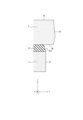
- 4 is a cross-sectional view showing a configuration example of a substrate
- FIG. 3 is an enlarged view of a portion enclosed by a broken line in FIG. 2
- FIG. FIG. 4 is a cross-sectional view showing a configuration example in which the upper surface of the wavelength conversion member is concave
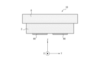
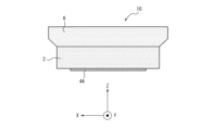
- FIG. 4 is a cross-sectional view showing a configuration example in which the corners of the wavelength conversion member are chamfered
- It is an example of a cross-sectional view by a cross section along the YZ plane.
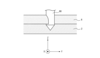
- FIG. 10 is a diagram showing a wavelength conversion member that is compressed and deformed by the side surface of a blade during dicing; It is a perspective view showing an example of composition of a lighting installation concerning one embodiment.
- the light-emitting device 10 includes an element substrate 2, a light-emitting element 3, and a wavelength conversion member 6.
- FIG. The light emitting element 3 is positioned on the side of the element substrate 2 in the positive direction of the Z axis.
- the wavelength conversion member 6 is located on the side of the element substrate 2 and the light emitting element 3 in the positive direction of the Z axis.
- the element substrate 2 has a first surface 2A facing the positive direction of the Z axis and a second surface 2B facing the negative direction of the Z axis.
- the side of the element substrate 2 in the positive direction of the Z axis is also referred to as the front side.
- the side of the element substrate 2 in the negative direction of the Z axis is also referred to as the back side.
- the element substrate 2 further includes a side surface 2C intersecting the first surface 2A and the second surface 2B.
- the side surface 2C of the element substrate 2 is also called a substrate side surface.
- the first surface 2A has sides that intersect with the side surface 2C.
- a side of the first surface 2A or a region within a predetermined distance from the side is also referred to as an end portion 2D of the first surface 2A.
- the element substrate 2 includes a first electrode 41 and a second electrode 42 on the first surface 2A on the front side.
- the first electrode 41 is located on the positive direction side of the X-axis with respect to the second electrode 42 .
- Two of each of the first electrodes 41 and the second electrodes 42 are positioned side by side along the Y-axis.
- the first electrode 41 and the second electrode 42 located on the positive direction side of the Y-axis are electrically connected.
- a first electrode 41 and a second electrode 42 positioned on the negative side of the Y-axis are electrically connected. That is, the element substrate 2 has two electrodes to which the first electrode 41 and the second electrode 42 are connected.
- the element substrate 2 has two rear surface electrodes 44 on the second surface 2B on the rear surface side.
- the two electrodes located on the front side and the two back electrodes 44 located on the back side are electrically connected to each other by wiring penetrating through the element substrate 2 .
- one electrode positioned on the front side in the positive direction of the Y axis and one rear surface electrode 44 positioned on the rear surface side in the positive direction of the Y axis are electrically connected.
- one electrode positioned on the front side in the negative direction of the Y axis and one rear surface electrode 44 positioned on the rear surface side in the negative direction of the Y axis are electrically connected.
- the element substrate 2 further includes a reflecting member 43 extending over a portion of the first surface 2A on the front side where the electrodes are not located.
- the reflecting member 43 extends to the edge 2D of the first surface 2A.
- the reflecting member 43 is positioned so as to surround the light emitting elements 3 .
- the light emitting element 3 is electrically connected to the first electrode 41 .
- the light emitting element 3 operates by power supplied from the back electrode 44 to the first electrode 41 .
- the light emitting element 3 emits light having a peak wavelength in a wavelength range of, for example, 360 nm or more and 430 nm or less.
- the wavelength range of 360 nm to 430 nm is also referred to as the violet light range.
- the wavelength conversion member 6 converts the light incident on the wavelength conversion member 6 from the light emitting element 3 into light having a peak wavelength in a wavelength range of 360 nm or more and 780 nm or less, for example, and emits the converted light.
- a wavelength region of 360 nm or more and 950 nm or less is also called a visible light region.
- the wavelength conversion member 6 emits a peak wavelength region in the visible light region by being excited by the light emitted by the light emitting element 3 .
- the light emitted by the light emitting element 3 is also called excitation light.
- the light emitting element 3 included in the light emitting device 10 is also called an excitation light emitting element.
- the light emitting device 10 may further include an electronic component 7.
- Electronic component 7 may be, for example, a Schottky diode.
- the electronic component 7 is electrically connected to the second electrodes 42 .
- the electronic component 7 is configured to be able to control the voltage between two electrodes located on the surface side.
- the first electrode 41 and the second electrode 42 are connected by a connecting conductor 45 .
- the element substrate 2 is also simply called a substrate.
- the element substrate 2 may be made of, for example, an insulating material.
- the element substrate 2 may be made of, for example, a ceramic material such as aluminum oxide (alumina) or mullite, a glass ceramic material, or a composite material obtained by mixing a plurality of these materials.
- the element substrate 2 may be formed of a polymer resin material or the like in which metal oxide fine particles are dispersed, the thermal expansion of which can be adjusted.
- the element substrate 2 may be configured including aluminum nitride or silicon carbide. Thereby, the thermal conductivity of the element substrate 2 can be improved, and the heat dissipation performance of the light emitting device 10 can be improved.
- the element substrate 2 is made of aluminum nitride.
- the first electrode 41, the second electrode 42, the back electrode 44, and the wiring penetrating the element substrate 2 may be made of a conductive material such as tungsten, molybdenum, manganese, or copper.
- the reflecting member 43 may be made of, for example, a material obtained by adding a white material such as titanium oxide to a silicone resin-based material.
- the reflecting member 43 is not limited to this example, and may be formed such that the reflectance of the reflecting member 43 is higher than the reflectance of the first surface 2A.
- the light emitting element 3 is an LED (Light Emitting Diode).
- An LED emits light to the outside by recombination of electrons and holes in a PN junction in which a P-type semiconductor and an N-type semiconductor are joined.
- the light-emitting elements 3 are not limited to LEDs, and may be other light-emitting devices.
- the light emitting element 3 is mounted on the first surface 2A of the element substrate 2.
- the light emitting element 3 is electrically connected to the first electrode 41 arranged on the first surface 2A of the element substrate 2 via, for example, brazing material or solder.
- Two of the first electrodes 41 are installed as one set so as to be connected to the positive and negative electrodes of the light emitting element 3 .
- the light-emitting element 3 is positioned on the first electrode 41 so as to cover at least a portion of the first electrode 41 in plan see-through of the first surface 2A of the element substrate 2 .
- the light-emitting element 3 may be larger than the first electrode 41 in planar see-through.
- the light emitting element 3 may be mounted on the element substrate 2 by flip chip bonding.
- the first electrode 41 and the brazing material, solder, or the like are positioned so as to be covered with the light emitting element 3 in plan view of the first surface 2A.
- the excitation light emitted from the light emitting element 3 or the illumination light converted by the wavelength conversion member 6 is transmitted to the first electrode 41 and the brazing material. Or, it becomes difficult to enter solder or the like.
- excitation light or illumination light is less likely to be absorbed by the first electrode 41 and the brazing material or solder.
- the luminous efficiency of the light emitting device 10 can be further enhanced.
- the light emitting element 3 when the light emitting element 3 is mounted on the element substrate 2 by wire bonding, at least part of the wire is not covered with the light emitting element 3 . In this case excitation light or illumination light can be absorbed in the wire.
- the light-emitting element 3 is mounted on the element substrate 2 by flip-chip bonding, so excitation light or illumination light is less likely to be absorbed than wire-bonding as in the comparative example. As a result, the luminous efficiency of the light emitting device 10 can be further enhanced.
- the number of light emitting elements 3 mounted on the first surface 2A of the element substrate 2 is one in FIG. 1 and the like, it is not particularly limited, and may be two or more. When the number of light emitting elements 3 is two or more, the respective light emitting elements 3 are positioned so as not to overlap each other in plan view of the first surface 2A.
- the light-emitting element 3 may include a translucent substrate and an optical semiconductor layer formed on the translucent substrate.
- the translucent substrate includes a material on which an optical semiconductor layer can be grown using, for example, metal-organic vapor phase epitaxy or chemical vapor deposition such as molecular beam epitaxy.
- the translucent substrate may be made of, for example, sapphire, gallium nitride, aluminum nitride, zinc oxide, zinc selenide, silicon carbide, silicon (Si), zirconium diboride, or the like.
- the thickness of the translucent substrate may be, for example, 50 ⁇ m or more and 1000 ⁇ m or less.
- the optical semiconductor layer may include a first semiconductor layer formed on the translucent substrate, a light emitting layer formed on the first semiconductor layer, and a second semiconductor layer formed on the light emitting layer.
- the first semiconductor layer, the light-emitting layer, and the second semiconductor layer are, for example, group III nitride semiconductors, group III-V semiconductors such as gallium phosphide or gallium arsenide, or group III semiconductors such as gallium nitride, aluminum nitride, or indium nitride. It may be formed of a nitride semiconductor or the like.
- the thickness of the first semiconductor layer may be, for example, 1 ⁇ m or more and 5 ⁇ m or less.
- the thickness of the light-emitting layer may be, for example, 25 nm or more and 150 nm or less.
- the thickness of the second semiconductor layer may be, for example, 50 nm or more and 600 nm or less.
- the wavelength converting member 6 is positioned on the first surface 2A of the element substrate 2. As shown in FIG. The wavelength conversion member 6 seals the light emitting element 3 by filling the space above the light emitting element 3 .
- the wavelength conversion member 6 may be formed by applying a paste on the first surface 2A of the element substrate 2 and then curing the paste.
- the wavelength conversion member 6 may be formed by being stuck on the first surface 2A of the element substrate 2 in the form of a sheet and then cured.
- the excitation light emitted from the light emitting element 3 directly enters the wavelength conversion member 6 .
- the wavelength conversion member 6 converts the incident excitation light into light having a peak wavelength within a wavelength range of, for example, 360 nm or more and 780 nm or less, and emits the converted light.
- the wavelength conversion member 6 may include a translucent member having translucency and a phosphor.
- the light-transmitting member may be made of, for example, a light-transmitting insulating resin material such as fluorine resin, silicone resin, acrylic resin, or epoxy resin, or a light-transmitting glass material.
- the refractive index of the translucent member may be set to 1.4 or more and 1.6 or less, for example.
- the phosphor is contained inside the translucent member.
- the phosphor may be dispersed substantially uniformly inside the translucent member.
- the phosphor converts incident excitation light into light having various peak wavelengths.
- the phosphor may convert the excitation light into spectrally specified light, ie, blue light, with a peak wavelength in the wavelength region of, for example, 400 nm to 500 nm.
- the phosphor is , for example, BaMgAl10O17 :Eu, or (Sr , Ca,Ba) 10 ( PO4 ) 6Cl2 :Eu, (Sr,Ba) 10 ( PO4 ) 6Cl2 :Eu and other materials.
- the phosphor may convert the excitation light into spectrally specified light, ie, blue-green light, with a peak wavelength in the wavelength region of, for example, 450 nm to 550 nm.
- the phosphor may include materials such as (Sr, Ba, Ca) 5 (PO 4 ) 3 Cl:Eu, Sr 4 Al 14 O 25 :Eu, for example.
- the phosphor may convert the excitation light into spectrally specified light, green light, with a peak wavelength in, for example, the 500 nm to 600 nm wavelength region.
- the phosphor is, for example, SrSi 2 (O, Cl) 2 N 2 :Eu, (Sr, Ba, Mg) 2 SiO 4 :Eu 2+ , or ZnS:Cu, Al, Zn 2 SiO 4 :Mn, or the like. may contain materials of
- the phosphor may convert the excitation light into spectrally specified light, ie, red light, having a peak wavelength in the wavelength region of, for example, 600 nm to 700 nm.
- the phosphor may include materials such as, for example, Y2O2S :Eu, Y2O3 :Eu, SrCaClAlSiN3 : Eu ⁇ 2+> , CaAlSiN3 :Eu, or CaAlSi(ON) 3 :Eu. .
- the phosphor may convert the excitation light into spectrally specified light, ie, near-infrared light, with a peak wavelength in the wavelength region of, for example, 680 nm to 800 nm.
- Near-infrared light may include light in the wavelength region from 680 to 2500 nm.
- the phosphor may include a material such as 3Ga 5 O 12 :Cr, for example.
- the combination of types of phosphors contained in the wavelength conversion member 6 is not particularly limited.
- the phosphor is not limited to the materials described above, and may include various other materials.
- the excitation light incident on the wavelength conversion member 6 from the light emitting element 3 is converted into light having different peak wavelengths depending on the phosphor.
- the peak wavelength of the converted light may fall within the visible light region.
- the converted light can have multiple peak wavelengths.
- the phosphors include a material that emits blue fluorescence, a material that emits blue-green fluorescence, and a material that emits green fluorescence
- the converted light will have blue, blue-green, and green wavelengths, respectively. It has a peak wavelength.
- the phosphor contains only one material, the converted light will have the peak wavelength of that material.
- the phosphor is not limited to these examples, and may include various combinations of materials.
- the color of light emitted from the wavelength conversion member 6 is determined based on the type of material contained in the phosphor. That is, the converted light can have different spectra.
- the light emitting device 10 can emit light having various spectra depending on the combination of materials contained in the phosphor.
- the light emitting device 10 emits light having, for example, the spectrum of direct sunlight from the sun, the spectrum of sunlight that reaches a predetermined depth in the sea, the spectrum of light emitted from a candle flame, or the spectrum of fluorescent light. can.
- the light emitting device 10 can emit light with various colors.
- the light emitting device 10 can emit light having various color temperatures.
- the wavelength conversion member 6 is positioned on the first surface 2A of the element substrate 2, and extends to the side where the first surface 2A intersects the side surface 2C in plan view of the first surface 2A.
- the wavelength converting member 6 contacts at least part of the first surface 2A.
- the wavelength converting member 6 is in contact with the first surface 2A via the reflecting member 43 in the portion where the reflecting member 43 is located on the first surface 2A.
- the wavelength converting member 6 may be in direct contact with the first surface 2A of the element substrate 2 or may be in contact with the first surface 2A via the reflecting member 43 .
- the wavelength conversion member 6 contacts at least the entire end portion 2D of the first surface 2A.
- the entire end portion 2D of the first surface 2A corresponds to the entire circumference of the side where the first surface 2A intersects the side surface 2C.
- the excitation light reflected by the first surface 2A or the reflecting member 43 always passes through the wavelength converting member 6 by the wavelength converting member 6 coming into contact with the end portion 2D of the first surface 2A.
- the wavelength conversion member 6 has a portion extending outward beyond at least a portion of the end portion 2D of the first surface 2A in a plan view of the first surface 2A. Since the wavelength conversion member 6 has a portion extending outward from the end portion 2D of the first surface 2A, the length of the excitation light passing through the wavelength conversion member 6 can be increased. As a result, the conversion efficiency of excitation light can be enhanced.
- the shape of the first surface 2A of the element substrate 2 may be rectangular.
- the shape of the first surface 2A is not limited to a rectangle and may be another polygon.
- the shape of the first surface 2A may be a figure having curved sides such as a circle or an ellipse.
- the wavelength conversion member 6 may spread outside each side of the first surface 2A of the element substrate 2 .
- the three-dimensional shape of the wavelength conversion member 6 may be rectangular parallelepiped. Thereby, the length of the excitation light passing through the wavelength conversion member 6 can be increased. As a result, the conversion efficiency of excitation light can be enhanced.
- the entire outer edge of the wavelength conversion member 6 may be positioned outside the sides of the element substrate 2 .
- the wavelength conversion member 6 has a top surface 6A facing the positive direction of the Z axis, a bottom surface 6B facing the negative direction of the Z axis, and side surfaces 6C intersecting the top surface 6A and the bottom surface 6B.
- the side surface 6C is also referred to as a wavelength conversion member side surface.
- the shape of the side surface of the wavelength conversion member may be convex toward the outside of the wavelength conversion member 6 in a cross-sectional view of at least one plane that intersects the first surface 2A of the element substrate 2 . Due to the convex shape of the side surface of the wavelength conversion member, the distance through which the excitation light passes through the wavelength conversion member 6 can be lengthened. As a result, the conversion efficiency of excitation light can be enhanced.
- the shape of both sides of the portion where the wavelength conversion member 6 spreads outward from the end portion 2D of the first surface 2A of the element substrate 2 may be different when the element substrate 2 is viewed in cross section.
- the shape of both sides of the portion of the wavelength conversion member 6 extending outward from the end portion 2D of the first surface 2A of the element substrate 2 is , the center line passing through the center of the wavelength conversion member 6 and extending in the stacking direction of the element substrate 2 and the wavelength conversion member 6 may be asymmetrical.
- the length by which the wavelength conversion member 6 protrudes outward may be different.
- the shape of 6 C of side surfaces of the wavelength conversion member 6 may differ.
- the surface roughness of the side surface 6C of the wavelength conversion member 6 may be made larger than the surface roughness of the side surface 2C of the element substrate 2 (substrate side surface).
- a mechanical external pressure is applied to the light emitting device 10 from the outside, the impact can be softened and the possibility of damage can be reduced.
- contact It may be appropriately selected according to the standard according to the size, material, etc. by the method of the formula or the method of the non-contact type.
- a scanning method using a stylus can be used
- non-contact type for example, an optical interference method, an image synthesizing method by focal point movement, a confocal method, or the like can be used.
- the reflecting member 43 has a side surface 43C continuing from the side surface 2C of the element substrate 2.
- 43 C of side surfaces of the reflecting member 43 are also called a reflecting member side surface.
- the side surface of the reflecting member inclines toward the wavelength converting member 6 from the side where the first surface 2A of the element substrate 2 intersects with the side surface 2C. In other words, the side surface of the reflecting member is inclined so as to enter the inside of the first surface 2A of the element substrate 2 as the distance from the first surface 2A of the element substrate 2 increases.
- the inclination of the side surface of the reflecting member increases the probability that the excitation light emitted from the bottom surface 6B of the wavelength converting member 6 is reflected by the side surface of the reflecting member and enters the bottom surface 6B of the wavelength converting member 6 .
- the conversion efficiency of excitation light can be enhanced.
- the upper surface 6A of the wavelength converting member 6 may be concave.
- the wavelength conversion member 6 in a plan view of the first surface 2A of the element substrate 2, the wavelength conversion member 6 has a concave surface that is recessed in a direction approaching the first surface 2A of the element substrate 2 at least in a portion that overlaps with the light emitting element 3. you can Since the upper surface 6A of the wavelength conversion member 6 is concave, the direction of illumination light emitted from the upper surface 6A of the wavelength conversion member 6 tends to be concentrated at the center of the concave surface.
- a chamfered shape may be provided at the corner where the bottom surface 6B and the side surface 6C intersect in the portion of the wavelength conversion member 6 that extends outward from the end portion 2D of the first surface 2A of the element substrate 2.
- the portion of the wavelength conversion member 6 that extends outward from the end 2D of the first surface 2A of the element substrate 2 is the element substrate in a cross-sectional view taken along at least one plane that intersects the first surface 2A of the element substrate 2.
- 2 may have a chamfered shape at the corners on the side closer to the first surface 2A.
- the chamfering shape may be C chamfering 6D as shown in FIG. 6 or may be R chamfering.
- the chamfered shape of the corners of the wavelength conversion member 6 may differ depending on the cross-sectional view direction. As shown in FIG. 7A, in a cross-sectional view of the light emitting device 10 along the YZ plane, the wavelength converting member 6 does not have chamfered corners. On the other hand, as shown in FIG. 7B, in a cross-sectional view of the light emitting device 10 along the ZX plane, the wavelength conversion member 6 has chamfered corners.
- the length of the portion of the wavelength conversion member 6 extending outward from the end 2D of the first surface 2A of the element substrate 2 is the same cross section. It may be 1% or more and 5% or less of the visual length of the element substrate 2 . By controlling the length in this way, the size of the light emitting device 10 can be controlled. If it is 1% or more, it is possible to reduce the risk of the element substrate 2 being directly impacted and damaged when mechanical external pressure is applied to the light emitting device 10 from the outside.
- the weight of the wavelength conversion member 6 itself can reduce the possibility that the portion extending outward from the element substrate 2 hangs down and deforms.
- the length here means, for example, the maximum length of the portion of the wavelength conversion member 6 extending outward from the end portion 2D of the element substrate 2 in the direction along the first surface 2A.
- the area of the light emitting element 3 may be made wider than the area of the first electrode 41.
- the light emitting element 3 may cover the entire first electrode 41 .
- the area of the electronic component 7 may be larger than the area of the second electrode 42 in plan view of the first surface 2A of the element substrate 2 .
- the electronic component 7 may cover the entire second electrode 42 . At least part of the wiring connecting the first electrode 41 and the second electrode 42 may be covered with the light emitting element 3 or the electronic component 7, or may be exposed in a plan view of the first surface 2A of the element substrate 2. good.
- the wavelength conversion member 6 can be configured in various shapes. By controlling the shape of the wavelength conversion member 6, the conversion efficiency of excitation light in the wavelength conversion member 6 or the luminous efficiency of the light emitting device 10 can be enhanced.
- a plurality of light emitting devices 10 according to this embodiment are formed on a wafer, for example, and are manufactured by dividing the wafer by dicing.
- the shape of the side surface 6C of the wavelength conversion member 6 or the side surface 2C of the element substrate 2 can be controlled by dicing conditions.
- Dicing is performed by inserting the disk-shaped blade 80 toward the object while rotating. As shown in FIG. 8A, the wavelength converting member 6 can be dragged in the direction of rotation of the dicing blade 80 . After the blade 80 passes through the wavelength conversion member 6, the wavelength conversion member 6 that has been dragged in the rotational direction of the blade 80 returns to its original position. On the other hand, since the element substrate 2 has a larger elastic modulus than the wavelength conversion member 6 , it is less likely to be dragged in the rotating direction of the blade 80 . As a result, the width of the portion of the wavelength conversion member 6 cut by dicing can be narrower than the width of the portion of the element substrate 2 cut by dicing.
- the dicing blade 80 can advance while pressing the wavelength converting member 6 with the side surface of the blade 80 when cutting the wavelength converting member 6 .
- the wavelength conversion member 6 is compressed in the normal direction of the side surface of the blade 80 .
- the wavelength conversion member 6 pressed by the side surface of the blade 80 returns to its original position.
- the element substrate 2 has a larger elastic modulus than the wavelength conversion member 6 , it is less likely to be dragged in the rotating direction of the blade 80 .
- the width of the portion of the wavelength conversion member 6 cut by dicing can be narrower than the width of the portion of the element substrate 2 cut by dicing.
- the wavelength conversion member 6 By narrowing the width of the cut portion of the wavelength conversion member 6 by dicing, the wavelength conversion member 6 is formed to have a portion extending outward from the end portion 2D of the first surface 2A of the element substrate 2.
- the difference between the width of the portion of the wavelength converting member 6 cut by dicing and the width of the portion of the element substrate 2 cut by dicing is due to the difference between the elastic modulus of the wavelength converting member 6 and the elastic modulus of the element substrate 2.
- the length of the portion where the wavelength conversion member 6 spreads outward from the end 2D of the first surface 2A of the element substrate 2 can be controlled by the difference between the elastic modulus of the wavelength conversion member 6 and the elastic modulus of the element substrate 2 . Since the elastic modulus of the wavelength converting member 6 is smaller than the elastic modulus of the element substrate 2 , the wavelength converting member 6 can be controlled to have a portion extending outward from the end 2D of the first surface 2A of the element substrate 2. .
- the dicing conditions include the rotational speed of the dicing blade 80, the speed at which the blade 80 is inserted into the wavelength conversion member 6 and the element substrate 2, the shape of the blade 80, and the like.
- the shape of the blade 80 is specified by, for example, the diameter, width or surface roughness of the blade 80 .
- Dicing conditions are also specified by which direction, the X-axis direction or the Y-axis direction, is cut first to cut out the light-emitting devices 10 from the wafer.
- the shape of the side surface 2C of the wavelength conversion member 6, the shape of the side surface 43C of the reflecting member 43, or the shape of the side surface 2C of the element substrate 2 can be controlled.
- the surface roughness of the side surface 6C of the wavelength conversion member 6 or the surface roughness of the side surface 2C of the element substrate 2 can be controlled.
- the convex shape of the side surface 6C of the wavelength conversion member 6 can be controlled.
- the chamfered shape of the corner of the wavelength conversion member 6 on the side closer to the first surface 2A of the element substrate 2 can be controlled.
- an illumination device 100 includes at least one light emitting device 10, and emits light emitted by the light emitting device 10 as illumination light.
- the intensity of light emitted by each light emitting device 10 may be controlled independently, or may be controlled in association with each other.
- the spectrum of the light emitted by each light emitting device 10 may be the same or different.
- the illumination device 100 may control the spectrum of light obtained by synthesizing the light emitted by each light emitting device 10 by controlling the intensity of the light emitted by each light emitting device 10 in association with each other.
- the illumination device 100 may emit synthetic light as illumination light.
- the illumination device 100 may select at least some of the plurality of light emitting devices 10 to emit illumination light.
- the lighting device 100 may further include a mounting board 110 on which the light emitting device 10 is mounted.
- the illumination device 100 may further include a housing 120 having a groove-shaped portion that accommodates the mounting plate 110 and a pair of end plates 130 closing the ends of the housing 120 on the short side.
- the number of light emitting devices 10 mounted on mounting board 110 may be one, or two or more.
- the light-emitting devices 10 may be mounted on the mounting board 110 so as to be arranged in a line, or may be mounted so as to be arranged in a grid pattern or a houndstooth pattern.
- the light-emitting device 10 is not limited to these patterns, and may be mounted on the mounting board 110 in various arrangement patterns.
- the mounting board 110 may include a circuit board having a wiring pattern.
- a circuit board may include, for example, a printed circuit board such as a rigid board, a flexible board, or a rigid-flexible board.
- the circuit board may include a drive circuit that controls the light emitting device 10 .
- the mounting board 110 has a function of dissipating the heat generated by the light emitting device 10 to the outside.
- the mounting board 110 may be made of, for example, a metal material such as aluminum, copper, or stainless steel, an organic resin material, or a composite material containing these materials.
- the mounting board 110 may have an elongated rectangular shape in plan view.
- the shape of the mounting board 110 is not limited to this and may be other various shapes.
- the lighting device 100 may further include a lid portion 140 that seals the mounting plate 110 and the light emitting device 10 housed inside the housing 120 .
- Lid portion 140 may transmit illumination light emitted from light emitting device 10 to the outside of lighting device 100 by being made of a translucent material.
- the lid portion 140 may be made of, for example, a resin material such as acrylic resin, glass, or the like.
- the lid portion 140 may have an elongated rectangular shape in plan view. The shape of the lid portion 140 is not limited to this and may be other various shapes.
- the lighting device 100 may further include a sealing member between the lid portion 140 and the housing 120 . By doing so, it becomes difficult for water, dust, or the like to enter the inside of the housing 120 . As a result, the reliability of lighting device 100 can be improved regardless of the environment in which lighting device 100 is installed.
- the lighting device 100 may further include a moisture absorbent inside the housing 120 .
- Descriptions such as “first” and “second” in this disclosure are identifiers for distinguishing the configurations. Configurations that are differentiated in descriptions such as “first” and “second” in this disclosure may interchange the numbers in that configuration.
- the first side 2A can exchange the identifiers “first” and “second” with the second side 23.
- FIG. The exchange of identifiers is done simultaneously.
- the configurations are still distinct after the exchange of identifiers.
- Identifiers may be deleted. Configurations from which identifiers have been deleted are distinguished by codes.
- the description of identifiers such as “first” and “second” in this disclosure should not be used as a basis for interpreting the order of the configuration or the existence of lower numbered identifiers.
- X-axis, Y-axis, and Z-axis are provided for convenience of explanation and may be interchanged with each other.
- Configurations according to the present disclosure have been described using a Cartesian coordinate system formed by X, Y, and Z axes.
- the positional relationship of each configuration according to the present disclosure is not limited to an orthogonal relationship.
Landscapes
- Physics & Mathematics (AREA)
- Spectroscopy & Molecular Physics (AREA)
- Engineering & Computer Science (AREA)
- General Engineering & Computer Science (AREA)
- Led Device Packages (AREA)
- Fastening Of Light Sources Or Lamp Holders (AREA)
Priority Applications (3)
| Application Number | Priority Date | Filing Date | Title |
|---|---|---|---|
| EP22876066.6A EP4411844A4 (en) | 2021-09-28 | 2022-09-22 | LIGHT-EMITTING DEVICE AND LIGHTING DEVICE |
| JP2023551433A JP7661513B2 (ja) | 2021-09-28 | 2022-09-22 | 発光装置及び照明装置 |
| JP2025061285A JP2025092709A (ja) | 2021-09-28 | 2025-04-02 | 発光装置及び照明装置 |
Applications Claiming Priority (2)
| Application Number | Priority Date | Filing Date | Title |
|---|---|---|---|
| JP2021-158465 | 2021-09-28 | ||
| JP2021158465 | 2021-09-28 |
Publications (1)
| Publication Number | Publication Date |
|---|---|
| WO2023054199A1 true WO2023054199A1 (ja) | 2023-04-06 |
Family
ID=85782611
Family Applications (1)
| Application Number | Title | Priority Date | Filing Date |
|---|---|---|---|
| PCT/JP2022/035505 Ceased WO2023054199A1 (ja) | 2021-09-28 | 2022-09-22 | 発光装置及び照明装置 |
Country Status (3)
| Country | Link |
|---|---|
| EP (1) | EP4411844A4 (https=) |
| JP (2) | JP7661513B2 (https=) |
| WO (1) | WO2023054199A1 (https=) |
Citations (12)
| Publication number | Priority date | Publication date | Assignee | Title |
|---|---|---|---|---|
| JP2002368286A (ja) * | 2001-06-11 | 2002-12-20 | Citizen Electronics Co Ltd | 発光ダイオード及びその製造方法 |
| WO2010044240A1 (ja) * | 2008-10-15 | 2010-04-22 | 株式会社小糸製作所 | 発光モジュール、発光モジュールの製造方法、および灯具ユニット |
| JP2011077551A (ja) * | 2010-12-29 | 2011-04-14 | Panasonic Electric Works Co Ltd | 発光装置 |
| JP2011258657A (ja) * | 2010-06-07 | 2011-12-22 | Toshiba Corp | 半導体発光装置および半導体発光装置の製造方法 |
| JP2012503876A (ja) * | 2008-09-25 | 2012-02-09 | コーニンクレッカ フィリップス エレクトロニクス エヌ ヴィ | コーティングされた発光デバイス及び発光デバイスをコーティングする方法 |
| JP2012528018A (ja) * | 2009-05-28 | 2012-11-12 | コーニンクレッカ フィリップス エレクトロニクス エヌ ヴィ | Lumiramic(登録商標)プレートレットのバレル研磨 |
| JP2013105877A (ja) * | 2011-11-14 | 2013-05-30 | Koito Mfg Co Ltd | 発光装置 |
| JP2016530725A (ja) * | 2013-08-20 | 2016-09-29 | コーニンクレッカ フィリップス エヌ ヴェKoninklijke Philips N.V. | 発光デバイス、基板及び方法 |
| JP2017063086A (ja) * | 2015-09-24 | 2017-03-30 | 株式会社小糸製作所 | 発光モジュール |
| JP2017224867A (ja) * | 2017-09-28 | 2017-12-21 | 日亜化学工業株式会社 | 発光装置及びその製造方法 |
| JP2019050359A (ja) | 2017-08-02 | 2019-03-28 | オスラム オプト セミコンダクターズ ゲゼルシャフト ミット ベシュレンクテル ハフツングOsram Opto Semiconductors GmbH | 発光半導体チップおよびオプトエレクトロニクスデバイス |
| JP2020061543A (ja) * | 2018-10-04 | 2020-04-16 | 日亜化学工業株式会社 | 発光装置 |
Family Cites Families (5)
| Publication number | Priority date | Publication date | Assignee | Title |
|---|---|---|---|---|
| JP2004071908A (ja) * | 2002-08-07 | 2004-03-04 | Matsushita Electric Works Ltd | 発光装置 |
| JP2008078225A (ja) * | 2006-09-19 | 2008-04-03 | Matsushita Electric Ind Co Ltd | 発光装置 |
| DE102010041236A1 (de) * | 2010-09-23 | 2012-03-29 | Osram Ag | Optoelektronisches Halbleiterbauelement |
| JP6850265B2 (ja) * | 2015-06-24 | 2021-03-31 | シーバラ アイピー アイ ビー.ブイ. | 蛍光体セラミック |
| JP2017079311A (ja) * | 2015-10-22 | 2017-04-27 | 豊田合成株式会社 | 発光装置の製造方法 |
-
2022
- 2022-09-22 WO PCT/JP2022/035505 patent/WO2023054199A1/ja not_active Ceased
- 2022-09-22 EP EP22876066.6A patent/EP4411844A4/en active Pending
- 2022-09-22 JP JP2023551433A patent/JP7661513B2/ja active Active
-
2025
- 2025-04-02 JP JP2025061285A patent/JP2025092709A/ja active Pending
Patent Citations (12)
| Publication number | Priority date | Publication date | Assignee | Title |
|---|---|---|---|---|
| JP2002368286A (ja) * | 2001-06-11 | 2002-12-20 | Citizen Electronics Co Ltd | 発光ダイオード及びその製造方法 |
| JP2012503876A (ja) * | 2008-09-25 | 2012-02-09 | コーニンクレッカ フィリップス エレクトロニクス エヌ ヴィ | コーティングされた発光デバイス及び発光デバイスをコーティングする方法 |
| WO2010044240A1 (ja) * | 2008-10-15 | 2010-04-22 | 株式会社小糸製作所 | 発光モジュール、発光モジュールの製造方法、および灯具ユニット |
| JP2012528018A (ja) * | 2009-05-28 | 2012-11-12 | コーニンクレッカ フィリップス エレクトロニクス エヌ ヴィ | Lumiramic(登録商標)プレートレットのバレル研磨 |
| JP2011258657A (ja) * | 2010-06-07 | 2011-12-22 | Toshiba Corp | 半導体発光装置および半導体発光装置の製造方法 |
| JP2011077551A (ja) * | 2010-12-29 | 2011-04-14 | Panasonic Electric Works Co Ltd | 発光装置 |
| JP2013105877A (ja) * | 2011-11-14 | 2013-05-30 | Koito Mfg Co Ltd | 発光装置 |
| JP2016530725A (ja) * | 2013-08-20 | 2016-09-29 | コーニンクレッカ フィリップス エヌ ヴェKoninklijke Philips N.V. | 発光デバイス、基板及び方法 |
| JP2017063086A (ja) * | 2015-09-24 | 2017-03-30 | 株式会社小糸製作所 | 発光モジュール |
| JP2019050359A (ja) | 2017-08-02 | 2019-03-28 | オスラム オプト セミコンダクターズ ゲゼルシャフト ミット ベシュレンクテル ハフツングOsram Opto Semiconductors GmbH | 発光半導体チップおよびオプトエレクトロニクスデバイス |
| JP2017224867A (ja) * | 2017-09-28 | 2017-12-21 | 日亜化学工業株式会社 | 発光装置及びその製造方法 |
| JP2020061543A (ja) * | 2018-10-04 | 2020-04-16 | 日亜化学工業株式会社 | 発光装置 |
Non-Patent Citations (1)
| Title |
|---|
| See also references of EP4411844A4 |
Also Published As
| Publication number | Publication date |
|---|---|
| JP2025092709A (ja) | 2025-06-19 |
| EP4411844A4 (en) | 2025-03-05 |
| JP7661513B2 (ja) | 2025-04-14 |
| EP4411844A1 (en) | 2024-08-07 |
| JPWO2023054199A1 (https=) | 2023-04-06 |
Similar Documents
| Publication | Publication Date | Title |
|---|---|---|
| JP5521325B2 (ja) | 発光装置及びその製造方法 | |
| TWI345842B (en) | Semiconductor light emitting device, method of manufacturing the same, and lighting apparatus and display apparatus using the same | |
| US11791441B2 (en) | Support structures for light emitting diode packages | |
| CN113039653B (zh) | 发光二极管封装 | |
| JP6015734B2 (ja) | 発光装置 | |
| US11101411B2 (en) | Solid-state light emitting devices including light emitting diodes in package structures | |
| JP5644967B2 (ja) | 発光装置及びその製造方法 | |
| JP6575828B2 (ja) | 発光装置及び発光モジュール | |
| JP2011222642A (ja) | 発光装置 | |
| JP5678462B2 (ja) | 発光装置 | |
| JP7661513B2 (ja) | 発光装置及び照明装置 | |
| JP2026503026A (ja) | 発光ダイオードデバイスの側壁配置および関連する方法 | |
| JP4947569B2 (ja) | 半導体発光素子及びその製造方法 | |
| JP7583816B2 (ja) | 発光装置及び照明装置 | |
| JP7483936B2 (ja) | 発光装置及び照明装置 | |
| JP5034342B2 (ja) | 発光装置 | |
| EP4618153A1 (en) | Light source module | |
| WO2022004564A1 (ja) | 発光装置及び照明装置 | |
| JP2008166311A (ja) | 半導体発光素子及び半導体発光装置 | |
| KR20190110356A (ko) | 반도체 소자 패키지 | |
| KR20220104656A (ko) | 발광 장치 | |
| JP2022010198A (ja) | 半導体発光装置 | |
| JP2020181999A (ja) | 半導体発光装置 |
Legal Events
| Date | Code | Title | Description |
|---|---|---|---|
| 121 | Ep: the epo has been informed by wipo that ep was designated in this application |
Ref document number: 22876066 Country of ref document: EP Kind code of ref document: A1 |
|
| WWE | Wipo information: entry into national phase |
Ref document number: 2023551433 Country of ref document: JP |
|
| NENP | Non-entry into the national phase |
Ref country code: DE |
|
| ENP | Entry into the national phase |
Ref document number: 2022876066 Country of ref document: EP Effective date: 20240429 |