WO2023048150A1 - 結晶膜の製造方法および結晶膜 - Google Patents
結晶膜の製造方法および結晶膜 Download PDFInfo
- Publication number
- WO2023048150A1 WO2023048150A1 PCT/JP2022/035038 JP2022035038W WO2023048150A1 WO 2023048150 A1 WO2023048150 A1 WO 2023048150A1 JP 2022035038 W JP2022035038 W JP 2022035038W WO 2023048150 A1 WO2023048150 A1 WO 2023048150A1
- Authority
- WO
- WIPO (PCT)
- Prior art keywords
- crystal
- plane
- film
- oxide
- substrate
- Prior art date
- Legal status (The legal status is an assumption and is not a legal conclusion. Google has not performed a legal analysis and makes no representation as to the accuracy of the status listed.)
- Ceased
Links
Images


Classifications
-
- C—CHEMISTRY; METALLURGY
- C23—COATING METALLIC MATERIAL; COATING MATERIAL WITH METALLIC MATERIAL; CHEMICAL SURFACE TREATMENT; DIFFUSION TREATMENT OF METALLIC MATERIAL; COATING BY VACUUM EVAPORATION, BY SPUTTERING, BY ION IMPLANTATION OR BY CHEMICAL VAPOUR DEPOSITION, IN GENERAL; INHIBITING CORROSION OF METALLIC MATERIAL OR INCRUSTATION IN GENERAL
- C23C—COATING METALLIC MATERIAL; COATING MATERIAL WITH METALLIC MATERIAL; SURFACE TREATMENT OF METALLIC MATERIAL BY DIFFUSION INTO THE SURFACE, BY CHEMICAL CONVERSION OR SUBSTITUTION; COATING BY VACUUM EVAPORATION, BY SPUTTERING, BY ION IMPLANTATION OR BY CHEMICAL VAPOUR DEPOSITION, IN GENERAL
- C23C16/00—Chemical coating by decomposition of gaseous compounds, without leaving reaction products of surface material in the coating, i.e. chemical vapour deposition [CVD] processes
- C23C16/04—Coating on selected surface areas, e.g. using masks
-
- C—CHEMISTRY; METALLURGY
- C23—COATING METALLIC MATERIAL; COATING MATERIAL WITH METALLIC MATERIAL; CHEMICAL SURFACE TREATMENT; DIFFUSION TREATMENT OF METALLIC MATERIAL; COATING BY VACUUM EVAPORATION, BY SPUTTERING, BY ION IMPLANTATION OR BY CHEMICAL VAPOUR DEPOSITION, IN GENERAL; INHIBITING CORROSION OF METALLIC MATERIAL OR INCRUSTATION IN GENERAL
- C23C—COATING METALLIC MATERIAL; COATING MATERIAL WITH METALLIC MATERIAL; SURFACE TREATMENT OF METALLIC MATERIAL BY DIFFUSION INTO THE SURFACE, BY CHEMICAL CONVERSION OR SUBSTITUTION; COATING BY VACUUM EVAPORATION, BY SPUTTERING, BY ION IMPLANTATION OR BY CHEMICAL VAPOUR DEPOSITION, IN GENERAL
- C23C16/00—Chemical coating by decomposition of gaseous compounds, without leaving reaction products of surface material in the coating, i.e. chemical vapour deposition [CVD] processes
- C23C16/22—Chemical coating by decomposition of gaseous compounds, without leaving reaction products of surface material in the coating, i.e. chemical vapour deposition [CVD] processes characterised by the deposition of inorganic material, other than metallic material
- C23C16/30—Deposition of compounds, mixtures or solid solutions, e.g. borides, carbides, nitrides
- C23C16/40—Oxides
-
- C—CHEMISTRY; METALLURGY
- C30—CRYSTAL GROWTH
- C30B—SINGLE-CRYSTAL GROWTH; UNIDIRECTIONAL SOLIDIFICATION OF EUTECTIC MATERIAL OR UNIDIRECTIONAL DEMIXING OF EUTECTOID MATERIAL; REFINING BY ZONE-MELTING OF MATERIAL; PRODUCTION OF A HOMOGENEOUS POLYCRYSTALLINE MATERIAL WITH DEFINED STRUCTURE; SINGLE CRYSTALS OR HOMOGENEOUS POLYCRYSTALLINE MATERIAL WITH DEFINED STRUCTURE; AFTER-TREATMENT OF SINGLE CRYSTALS OR A HOMOGENEOUS POLYCRYSTALLINE MATERIAL WITH DEFINED STRUCTURE; APPARATUS THEREFOR
- C30B23/00—Single-crystal growth by condensing evaporated or sublimed materials
- C30B23/02—Epitaxial-layer growth
- C30B23/04—Pattern deposit, e.g. by using masks
-
- C—CHEMISTRY; METALLURGY
- C30—CRYSTAL GROWTH
- C30B—SINGLE-CRYSTAL GROWTH; UNIDIRECTIONAL SOLIDIFICATION OF EUTECTIC MATERIAL OR UNIDIRECTIONAL DEMIXING OF EUTECTOID MATERIAL; REFINING BY ZONE-MELTING OF MATERIAL; PRODUCTION OF A HOMOGENEOUS POLYCRYSTALLINE MATERIAL WITH DEFINED STRUCTURE; SINGLE CRYSTALS OR HOMOGENEOUS POLYCRYSTALLINE MATERIAL WITH DEFINED STRUCTURE; AFTER-TREATMENT OF SINGLE CRYSTALS OR A HOMOGENEOUS POLYCRYSTALLINE MATERIAL WITH DEFINED STRUCTURE; APPARATUS THEREFOR
- C30B29/00—Single crystals or homogeneous polycrystalline material with defined structure characterised by the material or by their shape
- C30B29/10—Inorganic compounds or compositions
- C30B29/16—Oxides
-
- H—ELECTRICITY
- H10—SEMICONDUCTOR DEVICES; ELECTRIC SOLID-STATE DEVICES NOT OTHERWISE PROVIDED FOR
- H10P—GENERIC PROCESSES OR APPARATUS FOR THE MANUFACTURE OR TREATMENT OF DEVICES COVERED BY CLASS H10
- H10P14/00—Formation of materials, e.g. in the shape of layers or pillars
- H10P14/60—Formation of materials, e.g. in the shape of layers or pillars of insulating materials
Definitions
- the present invention relates to a crystalline film manufacturing method and a crystalline film useful for semiconductor devices.
- Patent Documents 10 and 11 describe that ELO crystal growth is performed using a PSS substrate to obtain a crystal film having a surface area of 9 ⁇ m 2 or more and a dislocation density of 5 ⁇ 10 6 cm ⁇ 2 .
- Patent Document 12 describes that after performing ELO crystal growth, a film and a substrate are separated using a separation sacrificial layer.
- Patent Documents 1 to 12 are all publications relating to patents or patent applications filed by the present applicants, and are still under investigation.
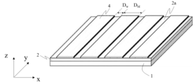
- the means for forming the convex portion may be known means, for example, known patterning processing means such as photolithography, electron beam lithography, laser patterning, nanoimprinting, and subsequent etching (e.g., dry etching, wet etching, etc.). etc.
- the convex portions are preferably stripe-shaped or dot-shaped, and more preferably dot-shaped.
- it is preferable that the formation of the convex portion is performed by forming a mask layer on the crystal substrate.
- the concave portion is not particularly limited, it may be made of the same material as the convex portion, or may be a substrate.
- the recess is preferably a void layer provided on the surface of the substrate.
- the means for forming the concave portion the same means as the means for forming the convex portion can be used.
- the void layer can be formed on the surface of the substrate by forming grooves in the substrate by a known groove processing means.
- the void layer can be preferably formed by, for example, forming a mask layer by sputtering, and then patterning using known patterning processing means such as photolithography.
- the groove width, groove depth, terrace width and the like of the void layer are not particularly limited as long as they do not interfere with the object of the present invention, and can be appropriately set.
- the “main component” means that the crystalline metal oxide is the atomic ratio of the first oxide crystal or It means that the content is preferably 50% or more, more preferably 70% or more, still more preferably 90% or more, and may be 100%, based on the total components of the second oxide crystal.
- a crystal film having a corundum structure can be obtained by performing the film formation using a substrate containing a corundum structure as the substrate.
- the crystalline metal oxide may be single crystal or polycrystal, but is preferably single crystal in the embodiment of the present invention.
- the upper limit of the thickness of the crystal film is not particularly limited. Although the lower limit of the thickness of the crystal film is not particularly limited, it is preferably 3 ⁇ m, more preferably 10 ⁇ m, and most preferably 20 ⁇ m.
- the n + -type region 970a may be formed using, for example, a known patterning method, a known film formation method, or a known impurity introduction method.
- Examples of the electrode 980a include metal materials selected from the group consisting of Al, Ti, Pt, Ru, Au, and alloys thereof.
- the Schottky electrode 1020 may be a metal material selected from the group consisting of Ni, Pt, Au, and alloys thereof.
- Ohmic electrode 1030 can be a metal material selected from the group consisting of Ti, In, and alloys thereof.
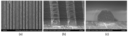
- the dislocations extending from the windows intersect the crystal meeting planes reach the crystal film surface in one ELO growth. It can be seen that, unlike the conventional ELO, a high dislocation density region is not formed on the crystal film surface. Further, from the planar TEM image of the obtained film, it was found that the dislocation density of the obtained crystal film was 7.3 ⁇ 10 5 /cm 2 in an area of at least 50 ⁇ m 2 (low dislocation density region). .
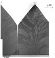
- the direction perpendicular to the plane of FIG. 9 (the a-axis direction) represents the direction of the a-axis projected onto the crystal growth plane (the plane perpendicular to the r-axis).
Landscapes
- Chemical & Material Sciences (AREA)
- Engineering & Computer Science (AREA)
- Materials Engineering (AREA)
- Metallurgy (AREA)
- Organic Chemistry (AREA)
- Crystallography & Structural Chemistry (AREA)
- General Chemical & Material Sciences (AREA)
- Chemical Kinetics & Catalysis (AREA)
- Mechanical Engineering (AREA)
- Inorganic Chemistry (AREA)
- Crystals, And After-Treatments Of Crystals (AREA)
Priority Applications (1)
| Application Number | Priority Date | Filing Date | Title |
|---|---|---|---|
| JP2022563129A JPWO2023048150A1 (https=) | 2021-09-22 | 2022-09-20 |
Applications Claiming Priority (2)
| Application Number | Priority Date | Filing Date | Title |
|---|---|---|---|
| JP2021-154914 | 2021-09-22 | ||
| JP2021154914 | 2021-09-22 |
Publications (1)
| Publication Number | Publication Date |
|---|---|
| WO2023048150A1 true WO2023048150A1 (ja) | 2023-03-30 |
Family
ID=85719487
Family Applications (1)
| Application Number | Title | Priority Date | Filing Date |
|---|---|---|---|
| PCT/JP2022/035038 Ceased WO2023048150A1 (ja) | 2021-09-22 | 2022-09-20 | 結晶膜の製造方法および結晶膜 |
Country Status (3)
| Country | Link |
|---|---|
| JP (1) | JPWO2023048150A1 (https=) |
| TW (1) | TW202319352A (https=) |
| WO (1) | WO2023048150A1 (https=) |
Citations (4)
| Publication number | Priority date | Publication date | Assignee | Title |
|---|---|---|---|---|
| JP2019151922A (ja) * | 2018-02-28 | 2019-09-12 | 株式会社Flosfia | 積層体および半導体装置 |
| CN110534555A (zh) * | 2019-08-26 | 2019-12-03 | 西安电子科技大学 | 基于r面Al2O3图形衬底的β-Ga2O3薄膜制作方法 |
| WO2020217563A1 (ja) * | 2019-04-24 | 2020-10-29 | 日本碍子株式会社 | 半導体膜 |
| WO2021153609A1 (ja) * | 2020-01-27 | 2021-08-05 | 株式会社Flosfia | 半導体装置および半導体装置の製造方法 |
-
2022
- 2022-09-20 JP JP2022563129A patent/JPWO2023048150A1/ja active Pending
- 2022-09-20 WO PCT/JP2022/035038 patent/WO2023048150A1/ja not_active Ceased
- 2022-09-21 TW TW111135729A patent/TW202319352A/zh unknown
Patent Citations (4)
| Publication number | Priority date | Publication date | Assignee | Title |
|---|---|---|---|---|
| JP2019151922A (ja) * | 2018-02-28 | 2019-09-12 | 株式会社Flosfia | 積層体および半導体装置 |
| WO2020217563A1 (ja) * | 2019-04-24 | 2020-10-29 | 日本碍子株式会社 | 半導体膜 |
| CN110534555A (zh) * | 2019-08-26 | 2019-12-03 | 西安电子科技大学 | 基于r面Al2O3图形衬底的β-Ga2O3薄膜制作方法 |
| WO2021153609A1 (ja) * | 2020-01-27 | 2021-08-05 | 株式会社Flosfia | 半導体装置および半導体装置の製造方法 |
Also Published As
| Publication number | Publication date |
|---|---|
| JPWO2023048150A1 (https=) | 2023-03-30 |
| TW202319352A (zh) | 2023-05-16 |
Similar Documents
| Publication | Publication Date | Title |
|---|---|---|
| JP7480937B2 (ja) | 結晶膜、半導体装置および結晶膜の製造方法 | |
| JP7166522B2 (ja) | 結晶膜の製造方法 | |
| CN109423690B (zh) | 用于制造结晶膜的方法 | |
| JP6945119B2 (ja) | 結晶性積層構造体およびその製造方法 | |
| JP7163540B2 (ja) | 結晶膜の製造方法 | |
| JP2016100593A (ja) | 結晶性積層構造体 | |
| JP7659153B2 (ja) | 結晶性積層構造体および半導体装置 | |
| JP7530054B2 (ja) | 結晶膜の製造方法 | |
| WO2023048150A1 (ja) | 結晶膜の製造方法および結晶膜 | |
| US11804519B2 (en) | Crystalline multilayer structure, semiconductor device, and method of manufacturing crystalline structure | |
| US20220189769A1 (en) | Crystal film, semiconductor device including crystal film, and method of producing crystal film | |
| JP7649944B2 (ja) | 結晶性積層構造体の製造方法 | |
| WO2021066156A1 (ja) | 結晶性積層構造体および半導体装置 | |
| JP7598113B2 (ja) | 結晶膜の成長方法および結晶性酸化物膜 | |
| US11694894B2 (en) | Crystalline film containing a crystalline metal oxide and method for manufacturing the same under partial pressure | |
| JP2025126924A (ja) | 結晶膜 | |
| JP7344426B2 (ja) | 結晶性積層構造体 | |
| JP2021080127A (ja) | 剥離方法および結晶性酸化物膜の製造方法 |
Legal Events
| Date | Code | Title | Description |
|---|---|---|---|
| WWE | Wipo information: entry into national phase |
Ref document number: 2022563129 Country of ref document: JP |
|
| 121 | Ep: the epo has been informed by wipo that ep was designated in this application |
Ref document number: 22872902 Country of ref document: EP Kind code of ref document: A1 |
|
| NENP | Non-entry into the national phase |
Ref country code: DE |
|
| 122 | Ep: pct application non-entry in european phase |
Ref document number: 22872902 Country of ref document: EP Kind code of ref document: A1 |