WO2023048150A1 - Method for producing crystal film, and crystal film - Google Patents
Method for producing crystal film, and crystal film Download PDFInfo
- Publication number
- WO2023048150A1 WO2023048150A1 PCT/JP2022/035038 JP2022035038W WO2023048150A1 WO 2023048150 A1 WO2023048150 A1 WO 2023048150A1 JP 2022035038 W JP2022035038 W JP 2022035038W WO 2023048150 A1 WO2023048150 A1 WO 2023048150A1
- Authority
- WO
- WIPO (PCT)
- Prior art keywords
- crystal
- plane
- film
- oxide
- substrate
- Prior art date
Links
- 239000013078 crystal Substances 0.000 title claims abstract description 318
- 238000004519 manufacturing process Methods 0.000 title claims abstract description 36
- 239000000758 substrate Substances 0.000 claims abstract description 122
- 239000004065 semiconductor Substances 0.000 claims abstract description 32
- 238000000034 method Methods 0.000 claims description 40
- 229910052593 corundum Inorganic materials 0.000 claims description 20
- 239000010431 corundum Substances 0.000 claims description 19
- GYHNNYVSQQEPJS-UHFFFAOYSA-N Gallium Chemical compound [Ga] GYHNNYVSQQEPJS-UHFFFAOYSA-N 0.000 claims description 16
- 229910052733 gallium Inorganic materials 0.000 claims description 16
- 239000010408 film Substances 0.000 description 154
- 239000007789 gas Substances 0.000 description 111
- 239000002184 metal Substances 0.000 description 48
- 229910052751 metal Inorganic materials 0.000 description 46
- 229910052760 oxygen Inorganic materials 0.000 description 24
- QVGXLLKOCUKJST-UHFFFAOYSA-N atomic oxygen Chemical compound [O] QVGXLLKOCUKJST-UHFFFAOYSA-N 0.000 description 22
- 239000001301 oxygen Substances 0.000 description 22
- 239000002994 raw material Substances 0.000 description 21
- 230000015572 biosynthetic process Effects 0.000 description 19
- 239000000463 material Substances 0.000 description 17
- 239000002019 doping agent Substances 0.000 description 16
- 229910052594 sapphire Inorganic materials 0.000 description 15
- 239000010980 sapphire Substances 0.000 description 15
- VEXZGXHMUGYJMC-UHFFFAOYSA-N Hydrochloric acid Chemical compound Cl VEXZGXHMUGYJMC-UHFFFAOYSA-N 0.000 description 13
- 239000010936 titanium Substances 0.000 description 13
- XOYLJNJLGBYDTH-UHFFFAOYSA-M chlorogallium Chemical compound [Ga]Cl XOYLJNJLGBYDTH-UHFFFAOYSA-M 0.000 description 12
- 229910052736 halogen Inorganic materials 0.000 description 12
- 150000002367 halogens Chemical class 0.000 description 12
- 229910001507 metal halide Inorganic materials 0.000 description 12
- 150000005309 metal halides Chemical class 0.000 description 12
- 229910052719 titanium Inorganic materials 0.000 description 12
- 229910005191 Ga 2 O 3 Inorganic materials 0.000 description 11
- 238000010586 diagram Methods 0.000 description 11
- 238000006243 chemical reaction Methods 0.000 description 10
- 238000000825 ultraviolet detection Methods 0.000 description 10
- 229910052782 aluminium Inorganic materials 0.000 description 9
- 150000004820 halides Chemical class 0.000 description 9
- 239000000470 constituent Substances 0.000 description 8
- 229910052732 germanium Inorganic materials 0.000 description 8
- IXCSERBJSXMMFS-UHFFFAOYSA-N hydrogen chloride Substances Cl.Cl IXCSERBJSXMMFS-UHFFFAOYSA-N 0.000 description 8
- 229910000041 hydrogen chloride Inorganic materials 0.000 description 8
- 229910052738 indium Inorganic materials 0.000 description 8
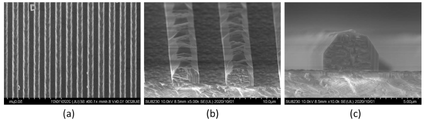
- 238000001878 scanning electron micrograph Methods 0.000 description 8
- 240000004050 Pentaglottis sempervirens Species 0.000 description 7
- 235000004522 Pentaglottis sempervirens Nutrition 0.000 description 7
- AJNVQOSZGJRYEI-UHFFFAOYSA-N digallium;oxygen(2-) Chemical compound [O-2].[O-2].[O-2].[Ga+3].[Ga+3] AJNVQOSZGJRYEI-UHFFFAOYSA-N 0.000 description 7
- 229910001195 gallium oxide Inorganic materials 0.000 description 7
- APFVFJFRJDLVQX-UHFFFAOYSA-N indium atom Chemical compound [In] APFVFJFRJDLVQX-UHFFFAOYSA-N 0.000 description 7
- 229910044991 metal oxide Inorganic materials 0.000 description 7
- 150000004706 metal oxides Chemical class 0.000 description 7
- 238000000206 photolithography Methods 0.000 description 7
- 229910052710 silicon Inorganic materials 0.000 description 7
- UPWPDUACHOATKO-UHFFFAOYSA-K gallium trichloride Chemical compound Cl[Ga](Cl)Cl UPWPDUACHOATKO-UHFFFAOYSA-K 0.000 description 6
- 230000002140 halogenating effect Effects 0.000 description 6
- 150000002739 metals Chemical class 0.000 description 6
- 239000003595 mist Substances 0.000 description 6
- 238000000059 patterning Methods 0.000 description 6
- BASFCYQUMIYNBI-UHFFFAOYSA-N platinum Chemical compound [Pt] BASFCYQUMIYNBI-UHFFFAOYSA-N 0.000 description 6
- PXHVJJICTQNCMI-UHFFFAOYSA-N Nickel Chemical compound [Ni] PXHVJJICTQNCMI-UHFFFAOYSA-N 0.000 description 5
- RTAQQCXQSZGOHL-UHFFFAOYSA-N Titanium Chemical compound [Ti] RTAQQCXQSZGOHL-UHFFFAOYSA-N 0.000 description 5
- 229910045601 alloy Inorganic materials 0.000 description 5
- 239000000956 alloy Substances 0.000 description 5
- XAGFODPZIPBFFR-UHFFFAOYSA-N aluminium Chemical compound [Al] XAGFODPZIPBFFR-UHFFFAOYSA-N 0.000 description 5
- 239000003795 chemical substances by application Substances 0.000 description 5
- 230000000052 comparative effect Effects 0.000 description 5
- GNPVGFCGXDBREM-UHFFFAOYSA-N germanium atom Chemical compound [Ge] GNPVGFCGXDBREM-UHFFFAOYSA-N 0.000 description 5
- 229910000039 hydrogen halide Inorganic materials 0.000 description 5
- 239000012433 hydrogen halide Substances 0.000 description 5
- 239000007769 metal material Substances 0.000 description 5
- 239000000203 mixture Substances 0.000 description 5
- 229910052697 platinum Inorganic materials 0.000 description 5
- 238000012545 processing Methods 0.000 description 5
- 238000004544 sputter deposition Methods 0.000 description 5
- 229910052720 vanadium Inorganic materials 0.000 description 5
- GPPXJZIENCGNKB-UHFFFAOYSA-N vanadium Chemical compound [V]#[V] GPPXJZIENCGNKB-UHFFFAOYSA-N 0.000 description 5
- 238000000927 vapour-phase epitaxy Methods 0.000 description 5
- 239000011800 void material Substances 0.000 description 5
- 229910052726 zirconium Inorganic materials 0.000 description 5
- CPELXLSAUQHCOX-UHFFFAOYSA-N Hydrogen bromide Chemical compound Br CPELXLSAUQHCOX-UHFFFAOYSA-N 0.000 description 4
- XEEYBQQBJWHFJM-UHFFFAOYSA-N Iron Chemical compound [Fe] XEEYBQQBJWHFJM-UHFFFAOYSA-N 0.000 description 4
- 229910004298 SiO 2 Inorganic materials 0.000 description 4
- XUIMIQQOPSSXEZ-UHFFFAOYSA-N Silicon Chemical compound [Si] XUIMIQQOPSSXEZ-UHFFFAOYSA-N 0.000 description 4
- 238000003917 TEM image Methods 0.000 description 4
- ATJFFYVFTNAWJD-UHFFFAOYSA-N Tin Chemical compound [Sn] ATJFFYVFTNAWJD-UHFFFAOYSA-N 0.000 description 4
- 239000012159 carrier gas Substances 0.000 description 4
- 238000005229 chemical vapour deposition Methods 0.000 description 4
- 238000005530 etching Methods 0.000 description 4
- 238000005498 polishing Methods 0.000 description 4
- 239000010703 silicon Substances 0.000 description 4
- 229910052718 tin Inorganic materials 0.000 description 4
- 229910018072 Al 2 O 3 Inorganic materials 0.000 description 3
- KRHYYFGTRYWZRS-UHFFFAOYSA-N Fluorane Chemical compound F KRHYYFGTRYWZRS-UHFFFAOYSA-N 0.000 description 3
- QCWXUUIWCKQGHC-UHFFFAOYSA-N Zirconium Chemical compound [Zr] QCWXUUIWCKQGHC-UHFFFAOYSA-N 0.000 description 3
- 230000005540 biological transmission Effects 0.000 description 3
- 150000001875 compounds Chemical class 0.000 description 3
- 238000002309 gasification Methods 0.000 description 3
- 238000005658 halogenation reaction Methods 0.000 description 3
- -1 hydrogen halides Chemical class 0.000 description 3
- XMBWDFGMSWQBCA-UHFFFAOYSA-N hydrogen iodide Chemical compound I XMBWDFGMSWQBCA-UHFFFAOYSA-N 0.000 description 3
- 229910052741 iridium Inorganic materials 0.000 description 3
- GKOZUEZYRPOHIO-UHFFFAOYSA-N iridium atom Chemical compound [Ir] GKOZUEZYRPOHIO-UHFFFAOYSA-N 0.000 description 3
- 229910052759 nickel Inorganic materials 0.000 description 3
- 229910052758 niobium Inorganic materials 0.000 description 3
- 239000010955 niobium Substances 0.000 description 3
- GUCVJGMIXFAOAE-UHFFFAOYSA-N niobium atom Chemical compound [Nb] GUCVJGMIXFAOAE-UHFFFAOYSA-N 0.000 description 3
- 229910052703 rhodium Inorganic materials 0.000 description 3
- 239000010948 rhodium Substances 0.000 description 3
- MHOVAHRLVXNVSD-UHFFFAOYSA-N rhodium atom Chemical compound [Rh] MHOVAHRLVXNVSD-UHFFFAOYSA-N 0.000 description 3
- 239000000126 substance Substances 0.000 description 3
- 238000001771 vacuum deposition Methods 0.000 description 3
- XKRFYHLGVUSROY-UHFFFAOYSA-N Argon Chemical compound [Ar] XKRFYHLGVUSROY-UHFFFAOYSA-N 0.000 description 2
- IJGRMHOSHXDMSA-UHFFFAOYSA-N Atomic nitrogen Chemical compound N#N IJGRMHOSHXDMSA-UHFFFAOYSA-N 0.000 description 2
- WKBOTKDWSSQWDR-UHFFFAOYSA-N Bromine atom Chemical compound [Br] WKBOTKDWSSQWDR-UHFFFAOYSA-N 0.000 description 2
- OKTJSMMVPCPJKN-UHFFFAOYSA-N Carbon Chemical compound [C] OKTJSMMVPCPJKN-UHFFFAOYSA-N 0.000 description 2
- VYZAMTAEIAYCRO-UHFFFAOYSA-N Chromium Chemical compound [Cr] VYZAMTAEIAYCRO-UHFFFAOYSA-N 0.000 description 2
- YCKRFDGAMUMZLT-UHFFFAOYSA-N Fluorine atom Chemical compound [F] YCKRFDGAMUMZLT-UHFFFAOYSA-N 0.000 description 2
- KDLHZDBZIXYQEI-UHFFFAOYSA-N Palladium Chemical compound [Pd] KDLHZDBZIXYQEI-UHFFFAOYSA-N 0.000 description 2
- 229910004541 SiN Inorganic materials 0.000 description 2
- VYPSYNLAJGMNEJ-UHFFFAOYSA-N Silicium dioxide Chemical compound O=[Si]=O VYPSYNLAJGMNEJ-UHFFFAOYSA-N 0.000 description 2
- 229910010413 TiO 2 Inorganic materials 0.000 description 2
- GDTBXPJZTBHREO-UHFFFAOYSA-N bromine Substances BrBr GDTBXPJZTBHREO-UHFFFAOYSA-N 0.000 description 2
- 229910052794 bromium Inorganic materials 0.000 description 2
- 229910052799 carbon Inorganic materials 0.000 description 2
- 229910052804 chromium Inorganic materials 0.000 description 2
- 239000011651 chromium Substances 0.000 description 2
- 229910017052 cobalt Inorganic materials 0.000 description 2
- 239000010941 cobalt Substances 0.000 description 2
- GUTLYIVDDKVIGB-UHFFFAOYSA-N cobalt atom Chemical compound [Co] GUTLYIVDDKVIGB-UHFFFAOYSA-N 0.000 description 2
- 239000010432 diamond Substances 0.000 description 2
- 229910003460 diamond Inorganic materials 0.000 description 2
- 229910052731 fluorine Inorganic materials 0.000 description 2
- 239000011737 fluorine Substances 0.000 description 2
- 229910052737 gold Inorganic materials 0.000 description 2
- 239000010931 gold Substances 0.000 description 2
- 229910052735 hafnium Inorganic materials 0.000 description 2
- 230000026030 halogenation Effects 0.000 description 2
- 238000010438 heat treatment Methods 0.000 description 2
- 239000001257 hydrogen Substances 0.000 description 2
- 229910052739 hydrogen Inorganic materials 0.000 description 2
- 229910000042 hydrogen bromide Inorganic materials 0.000 description 2
- 229910000043 hydrogen iodide Inorganic materials 0.000 description 2
- 239000012535 impurity Substances 0.000 description 2
- 239000011261 inert gas Substances 0.000 description 2
- 239000012212 insulator Substances 0.000 description 2
- 229910052742 iron Inorganic materials 0.000 description 2
- 238000005259 measurement Methods 0.000 description 2
- 150000001247 metal acetylides Chemical class 0.000 description 2
- 229910001510 metal chloride Inorganic materials 0.000 description 2
- 150000004767 nitrides Chemical class 0.000 description 2
- 229910052757 nitrogen Inorganic materials 0.000 description 2
- 239000012071 phase Substances 0.000 description 2
- 238000002360 preparation method Methods 0.000 description 2
- 239000010409 thin film Substances 0.000 description 2
- 238000002233 thin-film X-ray diffraction Methods 0.000 description 2
- ZCYVEMRRCGMTRW-UHFFFAOYSA-N 7553-56-2 Chemical compound [I] ZCYVEMRRCGMTRW-UHFFFAOYSA-N 0.000 description 1
- CPELXLSAUQHCOX-UHFFFAOYSA-M Bromide Chemical compound [Br-] CPELXLSAUQHCOX-UHFFFAOYSA-M 0.000 description 1
- KZBUYRJDOAKODT-UHFFFAOYSA-N Chlorine Chemical compound ClCl KZBUYRJDOAKODT-UHFFFAOYSA-N 0.000 description 1
- ZAMOUSCENKQFHK-UHFFFAOYSA-N Chlorine atom Chemical compound [Cl] ZAMOUSCENKQFHK-UHFFFAOYSA-N 0.000 description 1
- JMASRVWKEDWRBT-UHFFFAOYSA-N Gallium nitride Chemical compound [Ga]#N JMASRVWKEDWRBT-UHFFFAOYSA-N 0.000 description 1
- UFHFLCQGNIYNRP-UHFFFAOYSA-N Hydrogen Chemical compound [H][H] UFHFLCQGNIYNRP-UHFFFAOYSA-N 0.000 description 1
- KJTLSVCANCCWHF-UHFFFAOYSA-N Ruthenium Chemical compound [Ru] KJTLSVCANCCWHF-UHFFFAOYSA-N 0.000 description 1
- BQCADISMDOOEFD-UHFFFAOYSA-N Silver Chemical compound [Ag] BQCADISMDOOEFD-UHFFFAOYSA-N 0.000 description 1
- 230000002159 abnormal effect Effects 0.000 description 1
- PNEYBMLMFCGWSK-UHFFFAOYSA-N aluminium oxide Inorganic materials [O-2].[O-2].[O-2].[Al+3].[Al+3] PNEYBMLMFCGWSK-UHFFFAOYSA-N 0.000 description 1
- 229910052786 argon Inorganic materials 0.000 description 1
- 230000004888 barrier function Effects 0.000 description 1
- 150000001649 bromium compounds Chemical class 0.000 description 1
- 229910052801 chlorine Inorganic materials 0.000 description 1
- 239000000460 chlorine Substances 0.000 description 1
- 150000001805 chlorine compounds Chemical class 0.000 description 1
- 229910052681 coesite Inorganic materials 0.000 description 1
- 239000004020 conductor Substances 0.000 description 1
- 238000005336 cracking Methods 0.000 description 1
- 229910052906 cristobalite Inorganic materials 0.000 description 1
- 230000007547 defect Effects 0.000 description 1
- 238000000151 deposition Methods 0.000 description 1
- 238000001312 dry etching Methods 0.000 description 1
- 238000000609 electron-beam lithography Methods 0.000 description 1
- 238000000407 epitaxy Methods 0.000 description 1
- 238000011156 evaluation Methods 0.000 description 1
- 150000002222 fluorine compounds Chemical class 0.000 description 1
- PCHJSUWPFVWCPO-UHFFFAOYSA-N gold Chemical compound [Au] PCHJSUWPFVWCPO-UHFFFAOYSA-N 0.000 description 1
- CJNBYAVZURUTKZ-UHFFFAOYSA-N hafnium(IV) oxide Inorganic materials O=[Hf]=O CJNBYAVZURUTKZ-UHFFFAOYSA-N 0.000 description 1
- 229910000040 hydrogen fluoride Inorganic materials 0.000 description 1
- 239000012770 industrial material Substances 0.000 description 1
- 239000011810 insulating material Substances 0.000 description 1
- 238000011835 investigation Methods 0.000 description 1
- 150000004694 iodide salts Chemical class 0.000 description 1
- PNDPGZBMCMUPRI-UHFFFAOYSA-N iodine Chemical compound II PNDPGZBMCMUPRI-UHFFFAOYSA-N 0.000 description 1
- 239000011630 iodine Substances 0.000 description 1
- 229910052740 iodine Inorganic materials 0.000 description 1
- 230000001788 irregular Effects 0.000 description 1
- 239000007788 liquid Substances 0.000 description 1
- 239000007791 liquid phase Substances 0.000 description 1
- 230000008018 melting Effects 0.000 description 1
- 238000002844 melting Methods 0.000 description 1
- 239000012528 membrane Substances 0.000 description 1
- 150000002736 metal compounds Chemical class 0.000 description 1
- 238000002488 metal-organic chemical vapour deposition Methods 0.000 description 1
- 229910000510 noble metal Inorganic materials 0.000 description 1
- 230000003287 optical effect Effects 0.000 description 1
- 238000000879 optical micrograph Methods 0.000 description 1
- 229910052763 palladium Inorganic materials 0.000 description 1
- 230000000737 periodic effect Effects 0.000 description 1
- 230000000704 physical effect Effects 0.000 description 1
- 229910021420 polycrystalline silicon Inorganic materials 0.000 description 1
- 238000001552 radio frequency sputter deposition Methods 0.000 description 1
- 229910052707 ruthenium Inorganic materials 0.000 description 1
- 238000000926 separation method Methods 0.000 description 1
- 239000000377 silicon dioxide Substances 0.000 description 1
- 235000012239 silicon dioxide Nutrition 0.000 description 1
- 229910052814 silicon oxide Inorganic materials 0.000 description 1
- 229910052709 silver Inorganic materials 0.000 description 1
- 239000004332 silver Substances 0.000 description 1
- 239000007787 solid Substances 0.000 description 1
- 239000007921 spray Substances 0.000 description 1
- 229910052682 stishovite Inorganic materials 0.000 description 1
- 229910052723 transition metal Inorganic materials 0.000 description 1
- 150000003624 transition metals Chemical class 0.000 description 1
- 229910052905 tridymite Inorganic materials 0.000 description 1
- 239000012808 vapor phase Substances 0.000 description 1
- 230000008016 vaporization Effects 0.000 description 1
- 238000009834 vaporization Methods 0.000 description 1
- 238000001947 vapour-phase growth Methods 0.000 description 1
- 238000001039 wet etching Methods 0.000 description 1
- 229910001845 yogo sapphire Inorganic materials 0.000 description 1
- 229910052984 zinc sulfide Inorganic materials 0.000 description 1
Images


Classifications
-
- C—CHEMISTRY; METALLURGY
- C23—COATING METALLIC MATERIAL; COATING MATERIAL WITH METALLIC MATERIAL; CHEMICAL SURFACE TREATMENT; DIFFUSION TREATMENT OF METALLIC MATERIAL; COATING BY VACUUM EVAPORATION, BY SPUTTERING, BY ION IMPLANTATION OR BY CHEMICAL VAPOUR DEPOSITION, IN GENERAL; INHIBITING CORROSION OF METALLIC MATERIAL OR INCRUSTATION IN GENERAL
- C23C—COATING METALLIC MATERIAL; COATING MATERIAL WITH METALLIC MATERIAL; SURFACE TREATMENT OF METALLIC MATERIAL BY DIFFUSION INTO THE SURFACE, BY CHEMICAL CONVERSION OR SUBSTITUTION; COATING BY VACUUM EVAPORATION, BY SPUTTERING, BY ION IMPLANTATION OR BY CHEMICAL VAPOUR DEPOSITION, IN GENERAL
- C23C16/00—Chemical coating by decomposition of gaseous compounds, without leaving reaction products of surface material in the coating, i.e. chemical vapour deposition [CVD] processes
- C23C16/04—Coating on selected surface areas, e.g. using masks
-
- C—CHEMISTRY; METALLURGY
- C23—COATING METALLIC MATERIAL; COATING MATERIAL WITH METALLIC MATERIAL; CHEMICAL SURFACE TREATMENT; DIFFUSION TREATMENT OF METALLIC MATERIAL; COATING BY VACUUM EVAPORATION, BY SPUTTERING, BY ION IMPLANTATION OR BY CHEMICAL VAPOUR DEPOSITION, IN GENERAL; INHIBITING CORROSION OF METALLIC MATERIAL OR INCRUSTATION IN GENERAL
- C23C—COATING METALLIC MATERIAL; COATING MATERIAL WITH METALLIC MATERIAL; SURFACE TREATMENT OF METALLIC MATERIAL BY DIFFUSION INTO THE SURFACE, BY CHEMICAL CONVERSION OR SUBSTITUTION; COATING BY VACUUM EVAPORATION, BY SPUTTERING, BY ION IMPLANTATION OR BY CHEMICAL VAPOUR DEPOSITION, IN GENERAL
- C23C16/00—Chemical coating by decomposition of gaseous compounds, without leaving reaction products of surface material in the coating, i.e. chemical vapour deposition [CVD] processes
- C23C16/22—Chemical coating by decomposition of gaseous compounds, without leaving reaction products of surface material in the coating, i.e. chemical vapour deposition [CVD] processes characterised by the deposition of inorganic material, other than metallic material
- C23C16/30—Deposition of compounds, mixtures or solid solutions, e.g. borides, carbides, nitrides
- C23C16/40—Oxides
-
- C—CHEMISTRY; METALLURGY
- C30—CRYSTAL GROWTH
- C30B—SINGLE-CRYSTAL GROWTH; UNIDIRECTIONAL SOLIDIFICATION OF EUTECTIC MATERIAL OR UNIDIRECTIONAL DEMIXING OF EUTECTOID MATERIAL; REFINING BY ZONE-MELTING OF MATERIAL; PRODUCTION OF A HOMOGENEOUS POLYCRYSTALLINE MATERIAL WITH DEFINED STRUCTURE; SINGLE CRYSTALS OR HOMOGENEOUS POLYCRYSTALLINE MATERIAL WITH DEFINED STRUCTURE; AFTER-TREATMENT OF SINGLE CRYSTALS OR A HOMOGENEOUS POLYCRYSTALLINE MATERIAL WITH DEFINED STRUCTURE; APPARATUS THEREFOR
- C30B23/00—Single-crystal growth by condensing evaporated or sublimed materials
- C30B23/02—Epitaxial-layer growth
- C30B23/04—Pattern deposit, e.g. by using masks
-
- C—CHEMISTRY; METALLURGY
- C30—CRYSTAL GROWTH
- C30B—SINGLE-CRYSTAL GROWTH; UNIDIRECTIONAL SOLIDIFICATION OF EUTECTIC MATERIAL OR UNIDIRECTIONAL DEMIXING OF EUTECTOID MATERIAL; REFINING BY ZONE-MELTING OF MATERIAL; PRODUCTION OF A HOMOGENEOUS POLYCRYSTALLINE MATERIAL WITH DEFINED STRUCTURE; SINGLE CRYSTALS OR HOMOGENEOUS POLYCRYSTALLINE MATERIAL WITH DEFINED STRUCTURE; AFTER-TREATMENT OF SINGLE CRYSTALS OR A HOMOGENEOUS POLYCRYSTALLINE MATERIAL WITH DEFINED STRUCTURE; APPARATUS THEREFOR
- C30B29/00—Single crystals or homogeneous polycrystalline material with defined structure characterised by the material or by their shape
- C30B29/10—Inorganic compounds or compositions
- C30B29/16—Oxides
-
- H—ELECTRICITY
- H01—ELECTRIC ELEMENTS
- H01L—SEMICONDUCTOR DEVICES NOT COVERED BY CLASS H10
- H01L21/00—Processes or apparatus adapted for the manufacture or treatment of semiconductor or solid state devices or of parts thereof
- H01L21/02—Manufacture or treatment of semiconductor devices or of parts thereof
- H01L21/02104—Forming layers
- H01L21/02107—Forming insulating materials on a substrate
Definitions
- the present invention relates to a crystalline film manufacturing method and a crystalline film useful for semiconductor devices.
- Patent Documents 10 and 11 describe that ELO crystal growth is performed using a PSS substrate to obtain a crystal film having a surface area of 9 ⁇ m 2 or more and a dislocation density of 5 ⁇ 10 6 cm ⁇ 2 .
- Patent Document 12 describes that after performing ELO crystal growth, a film and a substrate are separated using a separation sacrificial layer.
- Patent Documents 1 to 12 are all publications relating to patents or patent applications filed by the present applicants, and are still under investigation.
- the means for forming the convex portion may be known means, for example, known patterning processing means such as photolithography, electron beam lithography, laser patterning, nanoimprinting, and subsequent etching (e.g., dry etching, wet etching, etc.). etc.
- the convex portions are preferably stripe-shaped or dot-shaped, and more preferably dot-shaped.
- it is preferable that the formation of the convex portion is performed by forming a mask layer on the crystal substrate.
- the concave portion is not particularly limited, it may be made of the same material as the convex portion, or may be a substrate.
- the recess is preferably a void layer provided on the surface of the substrate.
- the means for forming the concave portion the same means as the means for forming the convex portion can be used.
- the void layer can be formed on the surface of the substrate by forming grooves in the substrate by a known groove processing means.
- the void layer can be preferably formed by, for example, forming a mask layer by sputtering, and then patterning using known patterning processing means such as photolithography.
- the groove width, groove depth, terrace width and the like of the void layer are not particularly limited as long as they do not interfere with the object of the present invention, and can be appropriately set.
- the “main component” means that the crystalline metal oxide is the atomic ratio of the first oxide crystal or It means that the content is preferably 50% or more, more preferably 70% or more, still more preferably 90% or more, and may be 100%, based on the total components of the second oxide crystal.
- a crystal film having a corundum structure can be obtained by performing the film formation using a substrate containing a corundum structure as the substrate.
- the crystalline metal oxide may be single crystal or polycrystal, but is preferably single crystal in the embodiment of the present invention.
- the upper limit of the thickness of the crystal film is not particularly limited. Although the lower limit of the thickness of the crystal film is not particularly limited, it is preferably 3 ⁇ m, more preferably 10 ⁇ m, and most preferably 20 ⁇ m.
- the n + -type region 970a may be formed using, for example, a known patterning method, a known film formation method, or a known impurity introduction method.
- Examples of the electrode 980a include metal materials selected from the group consisting of Al, Ti, Pt, Ru, Au, and alloys thereof.
- the Schottky electrode 1020 may be a metal material selected from the group consisting of Ni, Pt, Au, and alloys thereof.
- Ohmic electrode 1030 can be a metal material selected from the group consisting of Ti, In, and alloys thereof.
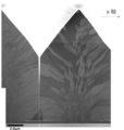
- the dislocations extending from the windows intersect the crystal meeting planes reach the crystal film surface in one ELO growth. It can be seen that, unlike the conventional ELO, a high dislocation density region is not formed on the crystal film surface. Further, from the planar TEM image of the obtained film, it was found that the dislocation density of the obtained crystal film was 7.3 ⁇ 10 5 /cm 2 in an area of at least 50 ⁇ m 2 (low dislocation density region). .
- the direction perpendicular to the plane of FIG. 9 (the a-axis direction) represents the direction of the a-axis projected onto the crystal growth plane (the plane perpendicular to the r-axis).
Abstract
Provided are a crystal film having excellent crystal quality, and a method for producing a high-quality crystal film with reduced dislocation, that are useful in semiconductor devices or the like. A method for producing a crystal film that includes forming uneven portions composed of recesses or protrusions on a crystal growth plane of a crystal substrate, either directly or with another layer interposed therebetween, and then forming a crystal film, wherein the crystal growth plane is inclined at an angle of less than 90 degrees from the c-plane, and the uneven portions are arranged along a direction parallel to the line of intersection of the crystal growth plane and the c-plane.
Description
本発明は、半導体装置に有用な結晶膜の製造方法および結晶膜に関する。
The present invention relates to a crystalline film manufacturing method and a crystalline film useful for semiconductor devices.
高耐圧、低損失および高耐熱を実現できる次世代のスイッチング素子として、バンドギャップの大きな酸化ガリウム(Ga2O3)を用いた半導体装置が注目されており、インバータなどの電力用半導体装置への適用が期待されている。また、広いバンドギャップからLEDやセンサー等の受発光装置としての幅広い応用も期待されている。特に、酸化ガリウムの中でもコランダム構造を有するα―Ga2O3等は、非特許文献1によると、インジウムやアルミニウムをそれぞれ、あるいは組み合わせて混晶とすることによりバンドギャップ制御することが可能であり、InAlGaO系半導体として極めて魅力的な材料系統を構成している。ここでInAlGaO系半導体とはInXAlYGaZO3(0≦X≦2、0≦Y≦2、0≦Z≦2、X+Y+Z=1.5~2.5)を示し(特許文献9等)、酸化ガリウムを内包する同一材料系統として俯瞰することができる。
Semiconductor devices using gallium oxide (Ga 2 O 3 ), which has a large bandgap, are attracting attention as next-generation switching elements that can achieve high withstand voltage, low loss, and high heat resistance, and are being applied to power semiconductor devices such as inverters. Application is expected. In addition, due to its wide bandgap, it is expected to be widely applied as light emitting and receiving devices such as LEDs and sensors. In particular, among gallium oxides, α-Ga 2 O 3 and the like, which have a corundum structure, can be controlled by forming a mixed crystal of indium and aluminum, respectively, or by combining them, according to Non-Patent Document 1. , constitutes an extremely attractive material system as an InAlGaO-based semiconductor. Here, the InAlGaO-based semiconductor indicates In X Al Y Ga ZO 3 (0≦X≦2, 0≦Y≦2, 0≦Z≦2, X+Y+Z=1.5 to 2.5) (Patent Document 9 etc.) can be viewed as the same material system including gallium oxide.
しかしながら、酸化ガリウムは、最安定相がβガリア構造であるので、特殊な成膜法を用いなければ、準安定相であるコランダム構造の結晶膜を成膜することが困難であり、例えば、ヘテロエピタキシャル成長等に結晶成長条件が制約されることも多く、そのため、転位密度が高くなる傾向がある。また、コランダム構造の結晶膜に限らず、成膜レートや結晶品質の向上、クラックや異常成長の抑制、ツイン抑制、反りによる基板の割れ等においてもまだまだ課題が数多く存在している。このような状況下、現在、コランダム構造を有する結晶性半導体の成膜について、いくつか検討がなされている。
However, since the most stable phase of gallium oxide is the β-gallia structure, it is difficult to form a crystalline film with a corundum structure, which is a metastable phase, unless a special film formation method is used. Crystal growth conditions are often restricted to epitaxial growth and the like, so the dislocation density tends to be high. In addition to the corundum structure crystal film, there are still many problems to be solved in improving the film formation rate and crystal quality, suppressing cracks and abnormal growth, suppressing twinning, and cracking the substrate due to warping. Under such circumstances, some studies are currently being conducted on film formation of a crystalline semiconductor having a corundum structure.
特許文献1には、ガリウム又はインジウムの臭化物又はヨウ化物を用いて、ミストCVD法により、酸化物結晶薄膜を製造する方法が記載されている。特許文献2~4には、コランダム型結晶構造を有する下地基板上に、コランダム型結晶構造を有する半導体層と、コランダム型結晶構造を有する絶縁膜とが積層された多層構造体が記載されている。また、特許文献5~7のように、ELO基板やボイド形成を用いて、ミストCVDによる成膜も検討されている。
特許文献8には、少なくとも、ガリウム原料と酸素原料とを用いて、ハライド気相成長法(HVPE法)により、コランダム構造を有する酸化ガリウムを成膜することが記載されている。また、特許文献10および11には、PSS基板を用いて、ELO結晶成長を行い、表面積は9μm2以上であり、転位密度が5×106cm-2の結晶膜を得ることが記載されている。また、特許文献12には、ELO結晶成長を行った後に剥離犠牲層を用いて膜と基板とを剥離することが記載されている。
なお、特許文献1~12はいずれも本出願人らによる特許または特許出願に関する公報であり、現在も検討が進められている。Patent Document 1 describes a method for producing an oxide crystal thin film by mist CVD using bromide or iodide of gallium or indium. Patent Documents 2 to 4 describe a multilayer structure in which a semiconductor layer having a corundum-type crystal structure and an insulating film having a corundum-type crystal structure are laminated on an underlying substrate having a corundum-type crystal structure. . Further, as in Patent Documents 5 to 7, film formation by mist CVD using an ELO substrate or void formation is being studied.
Patent Document 8 describes forming a film of gallium oxide having a corundum structure by a halide vapor phase epitaxy method (HVPE method) using at least a gallium source and an oxygen source. Further,Patent Documents 10 and 11 describe that ELO crystal growth is performed using a PSS substrate to obtain a crystal film having a surface area of 9 μm 2 or more and a dislocation density of 5×10 6 cm −2 . there is Further, Patent Document 12 describes that after performing ELO crystal growth, a film and a substrate are separated using a separation sacrificial layer.
Incidentally,Patent Documents 1 to 12 are all publications relating to patents or patent applications filed by the present applicants, and are still under investigation.
特許文献8には、少なくとも、ガリウム原料と酸素原料とを用いて、ハライド気相成長法(HVPE法)により、コランダム構造を有する酸化ガリウムを成膜することが記載されている。また、特許文献10および11には、PSS基板を用いて、ELO結晶成長を行い、表面積は9μm2以上であり、転位密度が5×106cm-2の結晶膜を得ることが記載されている。また、特許文献12には、ELO結晶成長を行った後に剥離犠牲層を用いて膜と基板とを剥離することが記載されている。
なお、特許文献1~12はいずれも本出願人らによる特許または特許出願に関する公報であり、現在も検討が進められている。
Patent Document 8 describes forming a film of gallium oxide having a corundum structure by a halide vapor phase epitaxy method (HVPE method) using at least a gallium source and an oxygen source. Further,
Incidentally,
本発明は、半導体装置等に有用な、転位が低減された高品質な結晶膜の製造方法および結晶品質に優れた結晶膜を提供することを目的とする。
An object of the present invention is to provide a method for manufacturing a high-quality crystalline film with reduced dislocations and a crystalline film with excellent crystal quality, which are useful for semiconductor devices and the like.
本発明者らは、上記目的を達成すべく鋭意検討した結果、結晶基板の結晶成長面上に、直接または他の層を介して、凹部または凸部からなる凹凸部を形成し、ついで、エピタキシャル膜を成膜して結晶性積層構造体を製造する方法において、前記結晶成長面が、c面から90度未満の角度で傾いた面であり、前記凹凸部が、前記結晶成長面とc面との交線と平行な方向に沿って配置されている製造方法を用いてエピタキシャル膜(結晶膜)を成膜すると、コランダム構造を有する結晶性酸化物半導体を主成分として含む結晶性酸化物膜であって、転位密度が1.0×10⁶/cm2以下であり、表面積が50μm2以上である結晶膜が得られることを知見し、このような結晶膜の製造方法および得られた結晶膜が上記した従来の問題を一挙に解決し得ることを見出した。
As a result of intensive studies to achieve the above object, the inventors of the present invention formed an uneven portion composed of concave portions or convex portions directly or via another layer on the crystal growth surface of the crystal substrate, and then epitaxially In the method of forming a film to manufacture a crystalline multilayer structure, the crystal growth plane is a plane inclined at an angle of less than 90 degrees from the c-plane, and the irregularities are formed between the crystal growth plane and the c-plane. When an epitaxial film (crystalline film) is formed using a manufacturing method arranged along a direction parallel to the line of intersection with and a crystal film having a dislocation density of 1.0×10 6 /cm 2 or less and a surface area of 50 μm 2 or more. We have found that the membrane can solve the above-mentioned conventional problems at once.
また、本発明者らは、上記知見を得た後、さらに検討を重ねて本発明を完成させるに至った。
In addition, after obtaining the above findings, the inventors conducted further studies and completed the present invention.
すなわち、本発明は、以下の発明に関する。
[1] 結晶基板の結晶成長面上に、直接または他の層を介して、凹部または凸部からなる凹凸部を形成し、ついで、結晶膜を成膜する結晶膜の製造方法であって、前記結晶成長面が、c面から90度未満の角度で傾いた面であり、前記凹凸部が、前記結晶成長面とc面との交線と平行な方向に沿って配置されていることを特徴とする結晶膜の製造方法。
[2] 前記結晶基板がコランダム構造を有する前記[1]記載の製造方法。
[3] 前記結晶成長面が、c面からa面またはm面の方向に90度未満の角度で傾いた面である前記[2]記載の製造方法。
[4] 前記交線がm軸またはa軸と平行である前記[2]または[3]に記載の製造方法。
[5] 前記結晶成長面が{10-1n}面、{-101n}面、{11-2m}面および{-1-12m}面(n、mは1以上の自然数)のいずれかである前記[2]~[4]のいずれかに記載の製造方法。
[6] 前記結晶成長面がr面である前記[2]~[5]のいずれかに記載の製造方法。
[7] 前記凹凸部が、m軸またはa軸に沿って配置されている前記[2]~[6]のいずれかに記載の製造方法。
[8] 前記凹凸部がa軸に沿って配置されている前記[2]~[7]のいずれかに記載の製造方法。
[9] コランダム構造を有する結晶性酸化物半導体を主成分として含む結晶膜であって、転位密度が1.0×10⁶/cm2以下である低転位領域を有し、該低転位領域の面積が50μm2以上であることを特徴とする結晶膜。
[10] 主面がr面である前記[9]記載の結晶膜。
[11] 第1の酸化物結晶と、該第1の酸化物結晶上に隣接して配置されている第2の酸化物結晶とを少なくも含む結晶膜であって、前記第1の酸化物結晶と前記第2の酸化物結晶との会合面が前記結晶膜表面と垂直な方向に対して傾斜していることを特徴とする結晶膜。
[12] 特定の方向に延びる転位線を含む第1の酸化物結晶と、前記第1の酸化物結晶上に隣接して配置されている第2の酸化物結晶とを少なくとも含む結晶膜であって、前記第1の酸化物結晶と前記第2の酸化物結晶との界面が前記転位線と交差していることを特徴とする結晶膜。
[13] 前記第1の酸化物結晶および/または前記第2の酸化物結晶がコランダム構造を有する前記[11]または[12]に記載の結晶膜。
[14] 前記第1の酸化物結晶および前記第2の酸化物結晶の主成分が同一である前記[11]~[13]のいずれかに記載の結晶膜。
[15] 前記第1の酸化物結晶および/または前記第2の酸化物結晶が、ガリウムを少なくとも含む前記[11]~[14]のいずれかに記載の結晶膜。
[16] 前記結晶膜表面が、c面から90度未満の角度で傾いた面である前記[9]~[15]のいずれかに記載の結晶膜。
[17] 電極および半導体層を少なくとも含む半導体装置であって、前記半導体層が、前記[9]~[16]のいずれかに記載の結晶膜を含むことを特徴とする半導体装置。 Specifically, the present invention relates to the following inventions.
[1] A method for producing a crystalline film by forming an uneven portion composed of concave portions or convex portions on a crystal growth surface of a crystalline substrate directly or via another layer, and then forming a crystalline film, comprising: The crystal growth plane is a plane inclined at an angle of less than 90 degrees from the c-plane, and the irregularities are arranged along a direction parallel to the line of intersection between the crystal growth plane and the c-plane. A method for producing a crystalline film characterized by:
[2] The manufacturing method according to [1], wherein the crystal substrate has a corundum structure.
[3] The production method according to [2] above, wherein the crystal growth plane is inclined from the c-plane toward the a-plane or the m-plane at an angle of less than 90 degrees.
[4] The manufacturing method according to [2] or [3], wherein the line of intersection is parallel to the m-axis or the a-axis.
[5] The crystal growth plane is any one of {10-1n} plane, {-101n} plane, {11-2m} plane and {-1-12m} plane (n and m are natural numbers of 1 or more). The production method according to any one of [2] to [4].
[6] The manufacturing method according to any one of [2] to [5], wherein the crystal growth plane is an r-plane.
[7] The manufacturing method according to any one of [2] to [6], wherein the uneven portion is arranged along the m-axis or the a-axis.
[8] The manufacturing method according to any one of [2] to [7], wherein the uneven portion is arranged along the a-axis.
[9] A crystalline film containing, as a main component, a crystalline oxide semiconductor having a corundum structure, having a low dislocation region with a dislocation density of 1.0×10 6 /cm 2 or less, wherein the low dislocation region is A crystalline film having an area of 50 μm 2 or more.
[10] The crystal film according to [9] above, wherein the main surface is an r-plane.
[11] A crystal film containing at least a first oxide crystal and a second oxide crystal arranged adjacently on the first oxide crystal, wherein the first oxide A crystal film, wherein a meeting plane between the crystal and the second oxide crystal is inclined with respect to a direction perpendicular to the surface of the crystal film.
[12] A crystal film including at least a first oxide crystal including dislocation lines extending in a specific direction and a second oxide crystal disposed adjacently on the first oxide crystal. A crystal film, wherein an interface between said first oxide crystal and said second oxide crystal intersects said dislocation line.
[13] The crystalline film according to [11] or [12], wherein the first oxide crystal and/or the second oxide crystal have a corundum structure.
[14] The crystal film according to any one of [11] to [13], wherein the first oxide crystal and the second oxide crystal have the same main component.
[15] The crystal film according to any one of [11] to [14], wherein the first oxide crystal and/or the second oxide crystal contain at least gallium.
[16] The crystalline film according to any one of [9] to [15], wherein the crystalline film surface is inclined at an angle of less than 90 degrees from the c-plane.
[17] A semiconductor device comprising at least an electrode and a semiconductor layer, wherein the semiconductor layer comprises the crystalline film according to any one of [9] to [16].
本発明の結晶膜の製造方法は、転位が低減された高品質の結晶膜を、簡単且つ容易に得ることができる。
The method for producing a crystalline film of the present invention can simply and easily obtain a high-quality crystalline film with reduced dislocations.
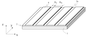
本発明の実施態様における結晶膜の製造方法は、結晶基板の結晶成長面上に、直接または他の層を介して、凹部または凸部からなる凹凸部を形成し、ついで、結晶膜を成膜する結晶膜の製造方法であって、前記結晶面が、c面から90度未満の角度で傾いた面であり、前記凹凸部が、前記結晶成長面とc面との交線と平行な方向に沿って配置して成膜を行うことを特長とする。ここで、c面は、{0001}面をいう。また、前記結晶成長面とは、前記結晶基板のうち、前記結晶膜が成膜される側の面(表面)をいう。
The method for producing a crystalline film according to an embodiment of the present invention comprises forming an uneven portion composed of concave portions or convex portions directly or via another layer on a crystal growth surface of a crystalline substrate, and then forming a crystalline film. wherein the crystal plane is inclined at an angle of less than 90 degrees from the c-plane, and the uneven portion is parallel to the intersection line between the crystal growth plane and the c-plane. It is characterized in that film formation is performed by arranging along the Here, the c plane refers to the {0001} plane. Further, the crystal growth surface refers to the surface (surface) of the crystal substrate on which the crystal film is formed.
(結晶基板)
前記結晶基板は、前記結晶基板の結晶成長面の少なくとも一部に結晶物を含む基板であれば、特に限定されず、公知の基板であってよい。本発明の実施態様においては、前記結晶基板が、結晶物を主成分として含む基板であるのが好ましい。前記結晶基板は、絶縁体基板であってもよいし、導電性基板であってもよいし、半導体基板であってもよい。また、前記結晶基板は、単結晶基板であってもよいし、多結晶基板であってもよい。本発明の実施態様においては、前記結晶基板が、単結晶基板であるのが好ましい。前記結晶基板としては、例えば、コランダム構造を有する結晶物を主成分として含む基板、またはβ-ガリア構造を有する結晶物を主成分として含む基板、六方晶構造を有する結晶物を主成分として含む基板などが挙げられる。本発明の実施態様においては、前記結晶基板が、{11-20}面(a面)または{10-10}面(m面)を含む結晶構造を有するのが好ましい。{11-20}面(a面)または{10-10}面(m面)を含む結晶構造としては、例えば、コランダム構造または六方晶構造(例えば、ε型構造、ウルツ鉱型構造等)等が挙げられる。なお、前記「主成分」とは、基板中の組成比で、前記結晶物を50%以上含むものをいい、好ましくは70%以上含むものであり、より好ましくは90%以上含むものである。 (crystal substrate)
The crystal substrate is not particularly limited as long as it contains crystals on at least part of the crystal growth surface of the crystal substrate, and may be a known substrate. In an embodiment of the present invention, it is preferable that the crystalline substrate is a substrate containing a crystalline substance as a main component. The crystal substrate may be an insulator substrate, a conductive substrate, or a semiconductor substrate. Further, the crystal substrate may be a single crystal substrate or a polycrystalline substrate. In an embodiment of the present invention, the crystal substrate is preferably a single crystal substrate. As the crystal substrate, for example, a substrate containing a crystal having a corundum structure as a main component, a substrate containing a crystal having a β-gallia structure as a main component, or a crystal having a hexagonal crystal structure as a main component. etc. In an embodiment of the present invention, the crystal substrate preferably has a crystal structure including a {11-20} plane (a-plane) or a {10-10} plane (m-plane). The crystal structure containing the {11-20} plane (a plane) or the {10-10} plane (m plane) includes, for example, a corundum structure or a hexagonal crystal structure (e.g., ε-type structure, wurtzite structure, etc.). is mentioned. The above-mentioned "main component" refers to a substrate containing 50% or more, preferably 70% or more, and more preferably 90% or more of the crystalline substance in terms of composition ratio in the substrate.
コランダム構造を有する結晶物を主成分として含む基板としては、例えば、サファイア基板、α型酸化ガリウム基板などが挙げられる。前記β-ガリア構造を有する結晶物を主成分として含む基板としては、例えば、β-Ga2O3基板、またはβ-Ga2O3とAl2O3とを含む混晶体基板などが挙げられる。なお、β-Ga2O3とAl2O3とを含む混晶体基板としては、例えば、Al2O3が原子比で0%より多くかつ60%以下含まれる混晶体基板などが好適な例として挙げられる。また、前記六方晶構造を有する基板としては、例えば、SiC基板、ZnO基板、GaN基板またはAlN基板などが挙げられる。その他の結晶基板の例示としては、例えば、Si基板などが挙げられる。
Examples of the substrate containing a crystal having a corundum structure as a main component include a sapphire substrate and an α-type gallium oxide substrate. Examples of the substrate containing the crystal having the β-gallia structure as a main component include a β-Ga 2 O 3 substrate and a mixed crystal substrate containing β-Ga 2 O 3 and Al 2 O 3 . . As the mixed crystal substrate containing β-Ga 2 O 3 and Al 2 O 3 , for example, a mixed crystal substrate containing more than 0% and 60% or less of Al 2 O 3 in atomic ratio is a suitable example. It is mentioned as. Moreover, examples of the substrate having the hexagonal crystal structure include a SiC substrate, a ZnO substrate, a GaN substrate, and an AlN substrate. Examples of other crystal substrates include, for example, Si substrates.
本発明の実施態様においては、前記結晶基板が、サファイア基板であるのが好ましい。前記サファイア基板としては、例えば、c面サファイア基板、m面サファイア基板、a面サファイア基板、r面サファイア基板などが挙げられる。本発明の実施態様においては、前記結晶基板が、r面サファイア基板であるのが好ましい。また、前記サファイア基板はオフ角を有していてもよい。前記オフ角は、特に限定されないが、好ましくは0°~15°である。なお、前記結晶基板の厚さは、特に限定されないが、好ましくは、50~2000μmであり、より好ましくは200~800μmである。
In an embodiment of the present invention, the crystal substrate is preferably a sapphire substrate. Examples of the sapphire substrate include a c-plane sapphire substrate, an m-plane sapphire substrate, an a-plane sapphire substrate, and an r-plane sapphire substrate. In an embodiment of the present invention, the crystal substrate is preferably an r-plane sapphire substrate. Moreover, the sapphire substrate may have an off angle. Although the off angle is not particularly limited, it is preferably 0° to 15°. Although the thickness of the crystal substrate is not particularly limited, it is preferably 50 to 2000 μm, more preferably 200 to 800 μm.
(凹凸部)
本発明においては、前記結晶基板上に、直接または他の層を介して、凹部または凸部からなる凹凸部を形成し、ついで、該凹凸部上に前記結晶膜を形成する。前記凹凸部は、前記結晶基板の結晶成長面上に直接形成されてもよいし、前記結晶基板の結晶成長面上に他の層(例えば、バッファ層等)を介して形成されてもよい。前記凹凸部は、凹部または凸部からなるものであれば特に限定されず、凹部からなる凹凸部であってもよいし、凸部からなる凹凸部であってもよい。また、前記凹凸部は、規則的な凹部または凸部から形成されていてもよいし、不規則な凹部または凸部から形成されていてもよい。本発明においては、前記凹凸部が周期的に形成されているのが好ましく、周期的かつ規則的にパターン化されているのがより好ましい。前記凹凸部の形状としては、特に限定されず、例えば、ストライプ状、ドット状、メッシュ状またはランダム状などが挙げられるが、本発明においては、ドット状またはストライプ状が好ましい。また、凹凸部が周期的かつ規則的にパターン化されている場合には、前記凹凸部のパターン形状が、三角形、四角形(例えば正方形、長方形若しくは台形等)、五角形若しくは六角形等の多角形状、円状、楕円状などの形状であるのが好ましい。前記凹凸部の凹部または凸部の断面形状としては、特に限定されないが、例えば、コの字型、U字型、逆U字型、波型、または三角形、四角形(例えば正方形、長方形若しくは台形等)、五角形若しくは六角形などの多角形等が挙げられる。 (Uneven part)
In the present invention, an uneven portion composed of concave portions or convex portions is formed directly or via another layer on the crystal substrate, and then the crystal film is formed on the uneven portion. The uneven portion may be formed directly on the crystal growth surface of the crystal substrate, or may be formed on the crystal growth surface of the crystal substrate via another layer (for example, a buffer layer or the like). The concave-convex portion is not particularly limited as long as it is formed of concave portions or convex portions. Further, the uneven portion may be formed from regular recesses or protrusions, or may be formed from irregular recesses or protrusions. In the present invention, the irregularities are preferably formed periodically, and more preferably patterned periodically and regularly. The shape of the uneven portion is not particularly limited, and examples thereof include stripes, dots, meshes, random shapes, etc. In the present invention, dots or stripes are preferable. Further, when the uneven portion is patterned periodically and regularly, the pattern shape of the uneven portion is a polygonal shape such as a triangle, a quadrangle (for example, a square, a rectangle, or a trapezoid), a pentagon, or a hexagon, A shape such as circular or elliptical is preferred. The cross-sectional shape of the concave portion or convex portion of the uneven portion is not particularly limited, but may be, for example, a U-shape, a U-shape, an inverted U-shape, a wave shape, a triangle, a quadrangle (e.g., a square, a rectangle, a trapezoid, etc.). ), polygons such as pentagons or hexagons.
前記凸部の構成材料は、特に限定されず、公知の材料であってよい。絶縁体材料であってもよいし、導電体材料であってもよいし、半導体材料であってもよい。また、前記構成材料は、非晶であってもよいし、単結晶であってもよいし、多結晶であってもよい。前記凸部の構成材料としては、例えば、Si、Ge、Ti、Zr、Hf、Ta、Sn等の酸化物、窒化物または炭化物、カーボン、ダイヤモンド、金属、これらの混合物などが挙げられる。より具体的には、SiO2、SiNまたは多結晶シリコンを主成分として含むSi含有化合物、前記結晶性酸化物の結晶成長温度よりも高い融点を有する金属(例えば、白金、金、銀、パラジウム、ロジウム、イリジウム、ルテニウムなどの貴金属等)などが挙げられる。本発明の実施態様においては、前記凸部の構成材料が、SiO2またはTiO2であるのが好ましい。なお、前記構成材料の含有量は、凸部中、組成比で、50%以上が好ましく、70%以上がより好ましく、90%以上が最も好ましい。
A constituent material of the convex portion is not particularly limited, and may be a known material. It may be an insulator material, a conductor material, or a semiconductor material. Further, the constituent material may be amorphous, single crystal, or polycrystalline. Examples of materials for forming the projections include oxides, nitrides or carbides of Si, Ge, Ti, Zr, Hf, Ta, Sn, carbon, diamond, metals, and mixtures thereof. More specifically, a Si-containing compound containing SiO 2 , SiN or polycrystalline silicon as a main component, a metal having a melting point higher than the crystal growth temperature of the crystalline oxide (e.g., platinum, gold, silver, palladium, Noble metals such as rhodium, iridium, ruthenium, etc.). In an embodiment of the present invention, it is preferable that the constituent material of the projections is SiO 2 or TiO 2 . The content of the constituent material is preferably 50% or more, more preferably 70% or more, and most preferably 90% or more in terms of composition ratio in the convex portion.
前記凸部の形成手段としては、公知の手段であってよく、例えば、フォトリソグラフィー、電子ビームリソグラフィー、レーザーパターニング、ナノインプリント、その後のエッチング(例えばドライエッチングまたはウェットエッチング等)などの公知のパターニング加工手段などが挙げられる。本発明においては、前記凸部がストライプ状またはドット状であるのが好ましく、ドット状であるのがより好ましい。また、本発明においては、
本発明の実施態様においては、前記凸部の形成を、前記結晶基板上にマスク層を形成することにより行うのが好ましい。マスク層は、例えば、真空蒸着法、CVD法またはスパッタリング法等の公知の成膜手段によってマスク層の構成材料を成膜した後、上記した公知のパターグ加工手段によって加工することにより好適に形成することができる。前記マスク層の構成材料としては、前記凸部の構成材料として例示した材料等が挙げられる。本発明においては、前記マスク層を用いて結晶膜を製造する場合、多結晶を少なくとも前記マスク層上に形成するのが、より厚膜且つより大面積の前記結晶性酸化物層を得ることができるので、好ましい。 The means for forming the convex portion may be known means, for example, known patterning processing means such as photolithography, electron beam lithography, laser patterning, nanoimprinting, and subsequent etching (e.g., dry etching, wet etching, etc.). etc. In the present invention, the convex portions are preferably stripe-shaped or dot-shaped, and more preferably dot-shaped. Moreover, in the present invention,
In an embodiment of the present invention, it is preferable that the formation of the convex portion is performed by forming a mask layer on the crystal substrate. The mask layer is suitably formed by, for example, forming a film of the constituent material of the mask layer by known film forming means such as vacuum deposition, CVD, or sputtering, and then processing the film by the above-described known pattern processing means. be able to. Examples of the constituent material of the mask layer include the materials exemplified as the constituent material of the convex portion. In the present invention, when a crystalline film is produced using the mask layer, polycrystals are formed at least on the mask layer to obtain a thicker and larger-area crystalline oxide layer. It is preferable because it can be done.
前記凹部は、特に限定されないが、上記凸部の構成材料と同様のものであってもよいし、基板であってもよい。本発明においては、前記凹部が、基板の表面上に設けられた空隙層であるのが好ましい。前記凹部の形成手段としては、前記凸部の形成手段と同様の手段を用いることができる。前記空隙層は、公知の溝加工手段により、基板に溝を設けることで、前記基板の表面上に形成することができる。本発明においては、前記空隙層を、例えば、スパッタリングによりマスク層を設けた後、ついで、フォトリソグラフィー等の公知のパターンニング加工手段を用いてパターニング加工することにより、好適に形成することができる。空隙層の溝幅、溝深さ、テラス幅等は、本発明の目的を阻害しない限り、特に限定されず、適宜に設定することができる。
Although the concave portion is not particularly limited, it may be made of the same material as the convex portion, or may be a substrate. In the present invention, the recess is preferably a void layer provided on the surface of the substrate. As the means for forming the concave portion, the same means as the means for forming the convex portion can be used. The void layer can be formed on the surface of the substrate by forming grooves in the substrate by a known groove processing means. In the present invention, the void layer can be preferably formed by, for example, forming a mask layer by sputtering, and then patterning using known patterning processing means such as photolithography. The groove width, groove depth, terrace width and the like of the void layer are not particularly limited as long as they do not interfere with the object of the present invention, and can be appropriately set.
前記結晶成長面は、c面から90度未満の角度で傾いた面であれば、本発明の目的を阻害しない限り、特に限定されない。本発明の実施態様においては、c面からa面またはm面の方向に90度未満の角度で傾いた面であるのが好ましい。前記結晶成長面のc面からの傾きの角度は、特に限定されない。本発明の実施態様においては、前記結晶成長面がc面から25°以上(90度未満)傾いた面であるのが好ましい。前記結晶成長面としては、例えば、{10-1n}面、{-101n}面、{11-2m}面または{-1-12m}面(n、mは1以上の自然数)等が挙げられる。本発明の実施態様においては、前記結晶成長面が、r面({-1012}面)、d面({-1014}面)、η面({10-12})面、R面({10-14}面)、S面({10-11})面またはn面({11-23}面)であるの好ましく、r面であるのがより好ましい。なお、前記結晶成長面は、オフ角(例えば、0°~15°)を有していてもよい。また、前記凹凸部は、前記結晶成長面とc面との交線と平行な方向に沿って配置されているものであれば、本発明の目的を阻害しない限り、特に限定されない。本発明の実施態様においては、前記交線がm軸またはa軸と平行であるのが好ましい。上記したような好ましい結晶成長面と、前記凹凸部の好ましい配置の方向とを組合わせることにより、表面に高転位密度領域を有しない高品質な結晶膜をより容易に得ることができる。なお、本明細書において表される「平行」とは、平行または略平行(±10°以内)の方向の場合も含む。また、「方向に沿って配置されている」とは、特定の方向に平行または略平行(±10°以内)の方向に沿って配置されることをいう。
The crystal growth plane is not particularly limited as long as it is a plane inclined at an angle of less than 90 degrees from the c-plane, as long as it does not hinder the object of the present invention. In an embodiment of the present invention, it is preferable that the surface is tilted from the c-plane toward the a-plane or the m-plane at an angle of less than 90 degrees. The inclination angle of the crystal growth plane from the c-plane is not particularly limited. In an embodiment of the present invention, the crystal growth plane is preferably a plane inclined by 25° or more (less than 90°) from the c-plane. Examples of the crystal growth plane include {10-1n} plane, {-101n} plane, {11-2m} plane and {-1-12m} plane (n and m are natural numbers of 1 or more). . In an embodiment of the present invention, the crystal growth plane is the r plane ({-1012} plane), the d plane ({-1014} plane), the η plane ({10-12}) plane, the R plane ({10 −14} plane), S plane ({10-11}) plane or n plane ({11-23} plane), more preferably r plane. The crystal growth surface may have an off angle (eg, 0° to 15°). Moreover, the irregularities are not particularly limited as long as they are arranged along a direction parallel to the line of intersection between the crystal growth plane and the c-plane, as long as the object of the present invention is not hindered. In an embodiment of the present invention, the line of intersection is preferably parallel to the m-axis or the a-axis. By combining the preferred crystal growth plane and the preferred arrangement direction of the irregularities as described above, it is possible to more easily obtain a high-quality crystal film that does not have a high dislocation density region on the surface. The term “parallel” used in this specification also includes parallel or substantially parallel (within ±10°) directions. Also, "arranged along a direction" means arranged along a direction parallel or substantially parallel (within ±10°) to a specific direction.
前記凹凸部は、上述のとおり、前記結晶成長面とc面との交線に平行な方向に沿って配置される。本発明の実施態様においては、前記結晶成長面が{10-1n}面または{-101n}面(nは1以上の自然数)である場合、である場合、前記凹凸部がa軸に沿って配置されるのが好ましい。また、前記結晶成長面が{11-2m}面または{-1-12m}面(mは1以上の自然数)である場合、前記凹凸部がm軸に沿って配置されるのが好ましい。
As described above, the irregularities are arranged along a direction parallel to the line of intersection between the crystal growth plane and the c-plane. In an embodiment of the present invention, when the crystal growth plane is a {10-1n} plane or a {-101n} plane (n is a natural number of 1 or more), the uneven portion is formed along the a-axis is preferably located. Further, when the crystal growth plane is the {11-2m} plane or the {-1-12m} plane (m is a natural number of 1 or more), the irregularities are preferably arranged along the m-axis.
以下、本発明の好ましい態様において用いられる結晶基板(凹凸部を含む)の例を、図面を用いて説明する。図2は、本発明の実施態様における結晶基板の結晶成長面上に設けられた凹凸部の一態様を示す。図2の凹凸部は、結晶基板1と、マスク層4とから構成されている。マスク層4は、結晶基板1の結晶成長面上にストライプ状に形成されており、マスク層4によって、凹部(溝)1aがストライプ状に形成されている。なお、マスク層4は、フォトリソグラフィー等の公知の手段を用いて形成することができる。また、マスク層4の構成材料としては、例えば、Si、Ge、Ti、例えば、Si、Ge、Ti、Zr、Hf、Ta、Sn、Al等の酸化物、窒化物または炭化物、カーボン、ダイヤモンド、金属、またはこれらの混合物等が挙げられる。本発明においては、前記マスク層4が、遷移金属の金属酸化物を含む場合、前記マスク層4が周期律表第4族金属を含むのが好ましく、Tiを含むのがより好ましい。また、本発明の実施態様においては、前記マスク層4が、SiO2またはTiO2を含むのが好ましい。
Hereinafter, examples of the crystal substrate (including uneven portions) used in preferred embodiments of the present invention will be described with reference to the drawings. FIG. 2 shows one aspect of the irregularities provided on the crystal growth surface of the crystal substrate in the embodiment of the present invention. The uneven portion in FIG. 2 is composed of a crystal substrate 1 and a mask layer 4 . The mask layer 4 is formed in stripes on the crystal growth surface of the crystal substrate 1, and the mask layer 4 forms recesses (grooves) 1a in stripes. The mask layer 4 can be formed using known means such as photolithography. The constituent material of the mask layer 4 includes, for example, Si, Ge, Ti, oxides, nitrides or carbides of Si, Ge, Ti, Zr, Hf, Ta, Sn, Al, etc., carbon, diamond, metals, mixtures thereof, and the like. In the present invention, when the mask layer 4 contains a metal oxide of a transition metal, the mask layer 4 preferably contains a Group 4 metal of the periodic table, more preferably Ti. Moreover, in the embodiment of the present invention, the mask layer 4 preferably contains SiO 2 or TiO 2 .
凹凸部の凸部(マスク層)の幅および高さ、間隔、凹部の幅および深さ、間隔などは特に限定されないが、本発明の実施態様においては、前記凸部(マスク層)の幅が約1μm~約1mmの範囲内であるのが好ましく、約5μm~約300μmの範囲内であるのがより好ましく、約10μm~約100μmの範囲内であるの最も好ましい。また、本発明の実施態様においては、前記凸部(マスク層)の高さが、約1nm~約1μmの範囲内であるのが好ましく、約5nm~約1μmの範囲内であるのより好ましく、約10nm~約100nmの範囲内であるのが最も好ましい。また、前記凸部(マスク層)の間隔は、約10nm~約300μmの範囲内であるのが好ましく、約100nm~約100μmの範囲内であるのがより好ましく、約1μm~約50μmの範囲内であるのが最も好ましい。また、本発明の実施態様においては、前記凹部の幅が、約10nm~約300μmであるのが好ましく、約100nm~約100μmであるのがより好ましく、約1μm~約50μmであるのが最も好ましい。また、本発明においては、前記凹部の深さが、約1nm~約1mmであるのが好ましく、約10nm~約300μmであるのがより好ましく、約20nm~約100μmであるのが最も好ましい。また、前記凹部の間隔は、約1μm~約1mmの範囲内であるのが好ましく、約5μm~約300μmの範囲内であるのがより好ましく、約10μm~約100μmの範囲内であるのが最も好ましい。前記凹凸部をこれら好ましいものとすることにより、より優れた前記結晶性積層構造体をより容易に得ることができる。なお、前記凹凸部は前記結晶基板上に直接形成されていてもよいし、他の層を介して設けられていてもよい。
The width, height and spacing of the protrusions (mask layer) of the protrusions and recesses, the width and depth of the recesses, the spacing and the like are not particularly limited. It is preferably in the range of about 1 μm to about 1 mm, more preferably in the range of about 5 μm to about 300 μm, and most preferably in the range of about 10 μm to about 100 μm. In an embodiment of the present invention, the height of the convex portion (mask layer) is preferably in the range of about 1 nm to about 1 μm, more preferably in the range of about 5 nm to about 1 μm, Most preferably it is in the range of about 10 nm to about 100 nm. Further, the interval between the convex portions (mask layer) is preferably in the range of about 10 nm to about 300 μm, more preferably in the range of about 100 nm to about 100 μm, and in the range of about 1 μm to about 50 μm. is most preferred. Further, in an embodiment of the present invention, the width of the recess is preferably about 10 nm to about 300 μm, more preferably about 100 nm to about 100 μm, most preferably about 1 μm to about 50 μm. . Further, in the present invention, the depth of the recess is preferably about 1 nm to about 1 mm, more preferably about 10 nm to about 300 μm, most preferably about 20 nm to about 100 μm. Also, the distance between the recesses is preferably in the range of about 1 μm to about 1 mm, more preferably in the range of about 5 μm to about 300 μm, most preferably in the range of about 10 μm to about 100 μm. preferable. By making the concave and convex portions preferable, a more excellent crystalline laminated structure can be obtained more easily. The uneven portion may be formed directly on the crystal substrate, or may be provided via another layer.
本発明においては、前記結晶基板上に応力緩和層等を含むバッファ層を設けてもよく、バッファ層を設ける場合には、バッファ層上に前記凹凸部を形成してもよい。また、本発明においては、前記結晶基板が、表面の一部または全部に、バッファ層を有しているのが好ましい。前記バッファ層の形成手段は、特に限定されず、公知の手段であってよい。前記形成手段としては、例えば、スプレー法、ミストCVD法、ミスト・エピタキシー法、HVPE法、MBE法、MOCVD法、MOVPE法、パルス成長法、ALD法またはスパッタリング法等が挙げられる。本発明においては、前記バッファ層が、ミストCVD法により形成されているのが、前記バッファ層上に形成される前記結晶膜の膜質をより優れたものとでき、特に、チルト等の結晶欠陥を抑制できるため、好ましい。
In the present invention, a buffer layer including a stress relieving layer and the like may be provided on the crystal substrate, and when the buffer layer is provided, the uneven portion may be formed on the buffer layer. Further, in the present invention, it is preferable that the crystal substrate has a buffer layer on part or all of its surface. A means for forming the buffer layer is not particularly limited, and may be a known means. Examples of the forming means include spray method, mist CVD method, mist epitaxy method, HVPE method, MBE method, MOCVD method, MOVPE method, pulse growth method, ALD method and sputtering method. In the present invention, the buffer layer is formed by the mist CVD method, so that the film quality of the crystal film formed on the buffer layer can be improved, and in particular, crystal defects such as tilt can be eliminated. It is preferable because it can be suppressed.
図3は、表面にバッファ層を介してマスク層が形成されている結晶基板を模式的に示す図である。図3の結晶基板1は、表面にバッファ層2を介してストライプ状の複数の窓を有するマスク層4が形成されており、前記マスク層の複数の窓2aは、線状に配置されている。本発明の実施態様においては、前記結晶基板1の結晶成長面が、c面から90度未満の角度で傾いた面であり、前記凹凸部(マスク層4)が、前記結晶成長面とc面との交線と平行な方向に沿って配置されている。ここで、前記結晶成長面は、図3のz軸方向と垂直な面であって、前記結晶基板1のバッファ層2が形成されている側の面である。すなわち、図3に示す実施形態においては、図3のz軸方向に垂直な面(結晶成長面)が、c面から90度未満の角度で傾いた面となる。前記結晶成長面としては、例えば、{10-1n}面、{-101n}面、{11-2m}面または{-1-12m}面(n、mは1以上の自然数)等が挙げられる。本発明の実施態様においては、前記結晶成長面が、r面、d面、η面、R面、S面またはn面であるの好ましく、r面であるのがより好ましい。また、前記凹凸部(マスク4)は、前記結晶成長面とc面との交線と平行な方向、すなわち、図3のy軸方向に沿って配置されている。図3のy軸方向は、例えば、m軸(m軸を結晶成長面上に投影した方向)またはa軸方向(a軸を結晶成長面上に投影した方向)である。
FIG. 3 is a diagram schematically showing a crystal substrate on which a mask layer is formed via a buffer layer. A mask layer 4 having a plurality of striped windows is formed on the surface of the crystal substrate 1 of FIG. 3 with a buffer layer 2 interposed therebetween. . In the embodiment of the present invention, the crystal growth plane of the crystal substrate 1 is a plane inclined at an angle of less than 90 degrees from the c-plane, and the uneven portion (mask layer 4) is located between the crystal growth plane and the c-plane. are arranged along the direction parallel to the line of intersection with Here, the crystal growth surface is a surface perpendicular to the z-axis direction in FIG. 3 and is the surface of the crystal substrate 1 on which the buffer layer 2 is formed. That is, in the embodiment shown in FIG. 3, the plane (crystal growth plane) perpendicular to the z-axis direction in FIG. 3 is inclined at an angle of less than 90 degrees from the c-plane. Examples of the crystal growth plane include {10-1n} plane, {-101n} plane, {11-2m} plane and {-1-12m} plane (n and m are natural numbers of 1 or more). . In an embodiment of the present invention, the crystal growth plane is preferably r-plane, d-plane, η-plane, R-plane, S-plane or n-plane, more preferably r-plane. Moreover, the irregularities (mask 4) are arranged in a direction parallel to the line of intersection between the crystal growth plane and the c-plane, that is, along the y-axis direction in FIG. The y-axis direction in FIG. 3 is, for example, the m-axis (the direction in which the m-axis is projected onto the crystal growth surface) or the a-axis direction (the direction in which the a-axis is projected onto the crystal growth surface).
前記窓の幅DWは、本発明の目的を阻害しない限り、特に限定されない。本発明の実施態様においては、前記窓の幅が、約10nm~約300μmの範囲内であるのが好ましく、約100nm~約100μmの範囲内であるのがより好ましく、約1μm~約50μmの範囲内であるのが最も好ましい。また、前記マスクの幅DMは、本発明の目的を阻害しない限り、特に限定されない。本発明の実施態様においては、前記マスクの幅DMが、約1μm~約1mmの範囲内であるのが好ましく、約5μm~約300μmの範囲内であるのがより好ましく、約10μm~約100μmの範囲内であるのが最も好ましい。なお、前記窓の幅DWは、前記マスクの幅DMよりも小さいのが好ましい。前記窓の幅および前記マスクの幅をこのような好ましい範囲内の値に設定することにより、前記結晶膜の品質をより優れたものとすることができる。
The width DW of the window is not particularly limited as long as it does not hinder the object of the present invention. In embodiments of the present invention, the width of said window is preferably in the range of about 10 nm to about 300 μm, more preferably in the range of about 100 nm to about 100 μm, and in the range of about 1 μm to about 50 μm. Most preferably within. Also, the width DM of the mask is not particularly limited as long as it does not interfere with the object of the present invention. In embodiments of the present invention, the width D M of the mask is preferably in the range of about 1 μm to about 1 mm, more preferably in the range of about 5 μm to about 300 μm, and more preferably in the range of about 10 μm to about 100 μm. is most preferably in the range of The width DW of the window is preferably smaller than the width DM of the mask. By setting the width of the window and the width of the mask to values within such preferable ranges, the quality of the crystal film can be made more excellent.
図4は、本発明の他の実施態様における、表面にバッファ層を介してマスクが形成されている基板を模式的に示す斜視図である。図4の結晶基板1は、表面にバッファ層2を介してドット状(円状)の複数の窓を有するマスク4が形成されており、前記マスクの複数の窓2aは、線状に配置されている。本発明の実施態様においては、前記結晶基板1の結晶成長面が、c面から90度未満の角度で傾いた面であり、前記凹凸部(マスク層4)が、前記結晶成長面とc面との交線と平行な方向に沿って配置されている。ここで、前記結晶成長面は、図4のz軸方向と垂直な面であって、前記結晶基板1のバッファ層2が形成されている側の面である。すなわち、図4に示す実施形態においては、図4のz軸方向に垂直な面(結晶成長面)が、c面から90度未満の角度で傾いた面となる。前記結晶成長面としては、例えば、{10-1n}面、{-101n}面、{11-2m}面または{-1-12m}面(n、mは1以上の自然数)等が挙げられる。本発明の実施態様においては、前記結晶成長面が、r面、d面、η面、R面、S面またはn面であるの好ましく、r面であるのがより好ましい。また、前記凹凸部(窓部2a)は、前記結晶成長面とc面との交線と平行な方向、すなわち、図4のy軸方向に沿って配置されている。図4のy軸方向は、例えば、m軸(m軸を結晶成長面上に投影した方向)またはa軸方向(a軸を結晶成長面上に投影した方向)である。前記のドット状の複数の窓は、隣接する列と各ドットの位置が半周期ずれるような配置であってもよい。また、前記ドットの平面形状は、円状に限定されず、例えば、略矩形状であってもよい。また、同じ列内の隣接するドット同士の間隔と、隣接する列同士の間隔との大小関係も、特に限定されない。本発明の実施態様においては、同じ列内の隣接するドット同士の間隔が、隣接する列同士の間隔よりも小さいのが好ましい。
FIG. 4 is a perspective view schematically showing a substrate having a mask formed on its surface via a buffer layer in another embodiment of the present invention. A mask 4 having a plurality of dot-shaped (circular) windows is formed on the surface of the crystal substrate 1 of FIG. 4 with a buffer layer 2 interposed therebetween. ing. In the embodiment of the present invention, the crystal growth plane of the crystal substrate 1 is a plane inclined at an angle of less than 90 degrees from the c-plane, and the uneven portion (mask layer 4) is located between the crystal growth plane and the c-plane. are arranged along the direction parallel to the line of intersection with Here, the crystal growth surface is a surface perpendicular to the z-axis direction in FIG. 4 and is the surface of the crystal substrate 1 on which the buffer layer 2 is formed. That is, in the embodiment shown in FIG. 4, the plane (crystal growth plane) perpendicular to the z-axis direction in FIG. 4 is a plane inclined at an angle of less than 90 degrees from the c-plane. Examples of the crystal growth plane include {10-1n} plane, {-101n} plane, {11-2m} plane and {-1-12m} plane (n and m are natural numbers of 1 or more). . In an embodiment of the present invention, the crystal growth plane is preferably r-plane, d-plane, η-plane, R-plane, S-plane or n-plane, more preferably r-plane. The irregularities (windows 2a) are arranged along the direction parallel to the line of intersection between the crystal growth plane and the c-plane, that is, along the y-axis direction in FIG. The y-axis direction in FIG. 4 is, for example, the m-axis (the direction in which the m-axis is projected onto the crystal growth surface) or the a-axis direction (the direction in which the a-axis is projected onto the crystal growth surface). The plurality of dot-shaped windows may be arranged such that the position of each dot in adjacent rows is shifted by half a cycle. Moreover, the planar shape of the dots is not limited to a circular shape, and may be, for example, a substantially rectangular shape. Also, the size relationship between the interval between adjacent dots in the same row and the interval between adjacent rows is not particularly limited. In embodiments of the present invention, the spacing between adjacent dots in the same column is preferably smaller than the spacing between adjacent columns.
本発明の実施態様においては、前記結晶基板の結晶成長面上に、直接または他の層を介して、前記凹凸部を形成した後、結晶膜を成膜する。前記結晶膜の成膜方法は、特に限定されず、公知の方法であってよい。前記結晶膜の成膜方法としては、例えば、HVPE法、ミストCVD法またはMOCVD法等が挙げられる。本発明の実施態様においては、前記結晶膜をHVPE法を用いて成膜するのが好ましい。
In an embodiment of the present invention, a crystal film is formed after forming the irregularities on the crystal growth surface of the crystal substrate directly or via another layer. A method for forming the crystal film is not particularly limited, and may be a known method. Examples of the method for forming the crystal film include HVPE method, mist CVD method, MOCVD method, and the like. In the embodiment of the present invention, it is preferable to form the crystal film using the HVPE method.
以下、前記結晶膜を成膜させる方法として、HVPE法を用いる場合を例として、本発明の実施態様をより詳細に説明する。前記HVPE法は、具体的には、例えば、図1に示す成膜装置を用いて、金属を含む金属源をガス化して金属ハロゲン化物ガスとし、ついで、前記金属ハロゲン化物ガスと、酸素含有原料ガスとを反応室の前記結晶基板に供給して成膜するのが好ましい。本発明の実施態様においては、反応性ガスを前記結晶基板上に供給し、前記成膜を前記反応性ガスの流通下で行うのも好ましい。
Hereinafter, the embodiment of the present invention will be described in more detail, taking as an example the case of using the HVPE method as the method for forming the crystal film. Specifically, for example, the HVPE method uses the film forming apparatus shown in FIG. It is preferable to form a film by supplying a gas to the crystal substrate in the reaction chamber. In an embodiment of the present invention, it is also preferable that a reactive gas is supplied onto the crystal substrate and the film formation is performed while the reactive gas is flowing.
(金属源)
前記金属源は、金属を含んでおり、ガス化が可能なものであれば、特に限定されず、金属単体であってもよいし、金属化合物であってもよい。前記金属としては、例えば、ガリウム、アルミニウム、インジウム、鉄、クロム、バナジウム、チタン、ロジウム、ニッケル、コバルトおよびイリジウム等から選ばれる1種または2種以上の金属等が挙げられる。本発明の実施態様においては、前記金属が、ガリウム、アルミニウムおよびインジウムから選らばれる1種または2種以上の金属であるのが好ましく、ガリウムであるのがより好ましく、前記金属源が、ガリウム単体であるのが最も好ましい。また、前記金属源は、気体であってもよいし、液体であってもよいし、固体であってもよい。 (metal source)
The metal source is not particularly limited as long as it contains a metal and can be gasified, and may be an elemental metal or a metal compound. Examples of the metal include one or more metals selected from gallium, aluminum, indium, iron, chromium, vanadium, titanium, rhodium, nickel, cobalt and iridium. In an embodiment of the present invention, the metal is preferably one or more metals selected from gallium, aluminum and indium, more preferably gallium, and the metal source is gallium alone. Most preferably. Also, the metal source may be gas, liquid, or solid.
前記ガス化の手段は、本発明の目的を阻害しない限り、特に限定されず、公知の手段であってよい。本発明の実施態様においては、前記ガス化の手段が、前記金属源をハロゲン化することにより行われるのが好ましい。前記ハロゲン化に用いるハロゲン化剤は、前記金属源をハロゲン化できさえすれば、特に限定されず、公知のハロゲン化剤であってよい。前記ハロゲン化剤としては、例えば、ハロゲンまたはハロゲン化水素等が挙げられる。前記ハロゲンとしては、例えば、フッ素、塩素、臭素、またはヨウ素等が挙げられる。また、ハロゲン化水素としては、例えば、フッ化水素、塩化水素、臭化水素、ヨウ化水素等が挙げられる。本発明の実施態様においては、前記ハロゲン化に、ハロゲン化水素を用いるのが好ましく、塩化水素を用いるのがより好ましい。本発明の実施態様においては、前記ガス化を、前記金属源に、ハロゲン化剤として、ハロゲンまたはハロゲン化水素を供給して、前記金属源とハロゲンまたはハロゲン化水素とをハロゲン化金属の気化温度以上で反応させてハロゲン化金属とすることにより行うのが好ましい。前記ハロゲン化反応温度は、特に限定されないが、本発明の実施態様においては、例えば、前記金属源がガリウムであり、前記ハロゲン化剤が、HClである場合には、900℃以下が好ましく、700℃以下がより好ましく、400℃~700℃であるのが最も好ましい。前記金属ハロゲン化物ガスは、前記金属源の金属のハロゲン化物を含むガスであれば、特に限定されない。前記金属ハロゲン化物ガスとしては、例えば、前記金属のハロゲン化物(フッ化物、塩化物、臭化物、ヨウ化物など)等が挙げられる。
The means for gasification is not particularly limited as long as it does not hinder the object of the present invention, and may be known means. In an embodiment of the present invention, said means for gasification is preferably carried out by halogenating said metal source. The halogenating agent used for the halogenation is not particularly limited as long as it can halogenate the metal source, and may be a known halogenating agent. Examples of the halogenating agent include halogens and hydrogen halides. Examples of the halogen include fluorine, chlorine, bromine, iodine, and the like. Hydrogen halides include, for example, hydrogen fluoride, hydrogen chloride, hydrogen bromide, and hydrogen iodide. In the embodiment of the present invention, hydrogen halide is preferably used for the halogenation, and hydrogen chloride is more preferably used. In an embodiment of the present invention, the gasification is performed by supplying a halogen or hydrogen halide as a halogenating agent to the metal source, and the metal source and the halogen or hydrogen halide are heated to the vaporization temperature of the metal halide. It is preferable to carry out by reacting as described above to form a metal halide. The halogenation reaction temperature is not particularly limited. °C or less is more preferred, and 400°C to 700°C is most preferred. The metal halide gas is not particularly limited as long as it contains a metal halide of the metal source. Examples of the metal halide gas include halides of the metals (fluorides, chlorides, bromides, iodides, etc.).
本発明の実施態様においては、金属を含む金属源をガス化して金属ハロゲン化物ガスとした後、前記金属ハロゲン化物ガスと、前記酸素含有原料ガスとを、前記反応室内の基板上に供給する。また、本発明の実施態様においては、反応性ガスを前記基板上に供給する。前記結晶層の形成温度は、特に限定されないが、本発明の実施態様においては、例えば、前記金属源がガリウムであり、前記ハロゲン化剤が、HClである場合には、900℃以下が好ましく、700℃以下がより好ましく、400℃~700℃であるのが最も好ましい。前記酸素含有原料ガスとしては、例えば、O2ガス、CO2ガス、NOガス、NO2ガス、N2Oガス、H2OガスまたはO3ガスから選ばれる1種または2種以上のガスである。本発明の実施態様においては、前記酸素含有原料ガスが、O2、H2OおよびN2Oからなる群から選ばれる1種または2種以上のガスであるのが好ましく、O2を含むのがより好ましい。前記反応性ガスは、通常、金属ハロゲン化物ガスおよび酸素含有原料ガスとは異なる反応性のガスであり、不活性ガスは含まれない。前記反応性ガスとしては、特に限定されないが、例えば、エッチングガス等が挙げられる。前記エッチングガスは、本発明の目的を阻害しない限り、特に限定されず、公知のエッチングガスであってよい。本発明の実施態様においては、前記反応性ガスが、ハロゲンガス(例えば、フッ素ガス、塩素ガス、臭素ガスまたはヨウ素ガス等)、ハロゲン化水素ガス(例えば、フッ酸ガス、塩酸ガス、臭化水素ガスまたはヨウ化水素ガス等)、水素ガスまたはこれら2種以上の混合ガス等であるのが好ましく、ハロゲン化水素ガスを含むのが好ましく、塩化水素を含むのが最も好ましい。なお、前記金属ハロゲン化物ガス、前記酸素含有原料ガス、前記反応性ガスは、キャリアガスを含んでいてもよい。前記キャリアガスとしては、例えば、窒素やアルゴン等の不活性ガス等が挙げられる。また、前記金属ハロゲン化物ガスの分圧は特に限定されないが、本発明の実施態様においては、0.5Pa~1kPaであるのが好ましく、5Pa~0.5kPaであるのがより好ましい。前記酸素含有原料ガスの分圧は、特に限定されないが、本発明の実施態様においては、前記金属ハロゲン化物ガスの分圧の0.5倍~100倍であるのが好ましく、1倍~20倍であるのがより好ましい。前記反応性ガスの分圧も、特に限定されないが、本発明の実施態様においては、前記金属ハロゲン化物ガスの分圧の0.1倍~5倍であるのが好ましく、0.2倍~3倍であるのがより好ましい。
In an embodiment of the present invention, after gasifying a metal source containing a metal into a metal halide gas, the metal halide gas and the oxygen-containing source gas are supplied onto the substrate in the reaction chamber. Also, in embodiments of the present invention, a reactive gas is supplied onto the substrate. The formation temperature of the crystal layer is not particularly limited, but in an embodiment of the present invention, for example, when the metal source is gallium and the halogenating agent is HCl, the temperature is preferably 900° C. or less, 700°C or less is more preferable, and 400°C to 700°C is most preferable. The oxygen-containing raw material gas is, for example, one or more gases selected from O2 gas, CO2 gas, NO gas, NO2 gas, N2O gas, H2O gas and O3 gas. be. In an embodiment of the present invention, the oxygen-containing raw material gas is preferably one or more gases selected from the group consisting of O 2 , H 2 O and N 2 O. is more preferred. The reactive gas is usually a reactive gas different from the metal halide gas and the oxygen-containing raw material gas, and does not contain an inert gas. Examples of the reactive gas include, but are not limited to, an etching gas. The etching gas is not particularly limited as long as it does not interfere with the object of the present invention, and may be a known etching gas. In an embodiment of the present invention, the reactive gas is a halogen gas (e.g., fluorine gas, chlorine gas, bromine gas, iodine gas, etc.), hydrogen halide gas (e.g., hydrofluoric acid gas, hydrochloric acid gas, hydrogen bromide gas or hydrogen iodide gas, etc.), hydrogen gas or a mixture of two or more of these, preferably containing hydrogen halide gas, and most preferably containing hydrogen chloride. In addition, the metal halide gas, the oxygen-containing raw material gas, and the reactive gas may contain a carrier gas. Examples of the carrier gas include inert gases such as nitrogen and argon. Although the partial pressure of the metal halide gas is not particularly limited, it is preferably 0.5 Pa to 1 kPa, more preferably 5 Pa to 0.5 kPa, in the embodiment of the present invention. The partial pressure of the oxygen-containing raw material gas is not particularly limited, but in the embodiment of the present invention, it is preferably 0.5 to 100 times, more preferably 1 to 20 times, the partial pressure of the metal halide gas. is more preferable. The partial pressure of the reactive gas is also not particularly limited, but in the embodiment of the present invention, it is preferably 0.1 to 5 times, more preferably 0.2 to 3 times, the partial pressure of the metal halide gas. Double is more preferable.
本発明の実施態様においては、さらに、ドーパント含有原料ガスを前記基板に供給するのも好ましい。前記ドーパント含有原料ガスは、ドーパントを含んでいれば、特に限定されない。前記ドーパントも、特に限定されないが、本発明の実施態様においては、前記ドーパントが、ゲルマニウム、ケイ素、チタン、ジルコニウム、バナジウム、ニオブおよびスズから選ばれる1種または2種以上の元素を含むのが好ましく、ゲルマニウム、ケイ素、またはスズを含むのがより好ましく、ゲルマニウムを含むのが最も好ましい。このようにドーパント含有原料ガスを用いることにより、得られる膜の導電率を容易に制御することができる。前記ドーパント含有原料ガスは、前記ドーパントを化合物(例えば、ハロゲン化物、酸化物等)の形態で有するのが好ましく、ハロゲン化物の形態で有するのがより好ましい。前記ドーパント含有原料ガスの分圧は、特に限定されないが、本発明の実施態様においては、前記金属含有原料ガスの分圧の1×10⁻⁷倍~0.1倍であるのが好ましく、2.5×10⁻⁶倍~7.5×10⁻²倍であるのがより好ましい。なお、本発明の実施態様においては、前記ドーパント含有原料ガスを、前記反応性ガスとともに前記基板上に供給するのが好ましい。
In embodiments of the present invention, it is also preferred to supply a dopant-containing source gas to the substrate. The dopant-containing raw material gas is not particularly limited as long as it contains a dopant. The dopant is also not particularly limited, but in the embodiment of the present invention, the dopant preferably contains one or more elements selected from germanium, silicon, titanium, zirconium, vanadium, niobium and tin. , germanium, silicon, or tin, most preferably germanium. By using the dopant-containing source gas in this manner, the conductivity of the resulting film can be easily controlled. The dopant-containing source gas preferably contains the dopant in the form of a compound (eg, halide, oxide, etc.), more preferably in the form of a halide. The partial pressure of the dopant-containing source gas is not particularly limited, but in the embodiment of the present invention, it is preferably 1×10 −7 to 0.1 times the partial pressure of the metal-containing source gas. It is more preferably 0.5×10 −6 times to 7.5×10 −2 times. In addition, in the embodiment of the present invention, it is preferable to supply the dopant-containing raw material gas onto the substrate together with the reactive gas.
上記した本発明の実施態様にかかる製造方法によれば、例えば、コランダム構造を有する結晶性酸化物半導体を主成分として含む結晶膜であって、転位密度が1.0×106/cm2以下である低転位領域を有し、該低転位領域の面積が50μm2以上であることを特徴とする結晶膜を得ることができる。また、上記した好ましい製造方法によれば、コランダム構造を有する結晶性酸化物半導体を主成分として含む結晶膜であって、転位密度が1.0×106/cm2以下であり、表面積が50μm2以上である結晶膜を得ることができる。前記転位密度は、貫通転位の密度をいい、表面(平面)TEM観察あるいはエッチピット観察によって測定できるものをいう。前記表面積は、通常、表面(平面)TEM(透過電子顕微鏡)像、SEM像、あるいは光学顕微鏡像から求められる面積をいう。本発明の実施態様においては、前記表面積が100μm2以上であるのが好ましい。前記結晶膜の主面は、c面から90度未満の角度で傾いた面であるのが好ましく、{10-1n}面、{-101n}面、{11-2m}面および{-1-12m}面(n、mは1以上の自然数)のいずれかであるのがより好ましく、r面であるのが最も好ましい。このような好ましい主面とすることにより、表面に高転位密度領域を有さない高品質な結晶膜を得ることができる。また、上記した本発明の実施態様にかかる製造方法によれば、例えば、第1の酸化物結晶と、該第1の酸化物結晶上に隣接して配置されている第2の酸化物結晶とを少なくも含む結晶膜であって、前記第1の酸化物結晶と前記第2の酸化物結晶との会合面が前記結晶膜表面と垂直な方向に対して傾斜していることを特長とする結晶膜を得ることができる。前記傾斜の角度は、特に限定されないが、本発明の実施態様においては、5°~75°であるのが好ましく、20°~60°であるのがより好ましい。さらに、上記した本発明の実施態様に係る製造方法によれば、特定の方向に延びる転位線を含む第1の酸化物結晶と、前記第1の酸化物結晶上に隣接して配置されている第2の酸化物結晶とを少なくとも含む結晶膜であって、前記第1の酸化物結晶と前記第2の酸化物結晶との界面が前記転位線と交差していることを特長とする結晶膜を得ることができる。ここで、転位線は、通常貫通転位の転位線をいう。また、転位線の向き等は、TEM(透過顕微鏡:Transmission Electron Microscope)観察法によって求められる。
According to the manufacturing method according to the embodiment of the present invention described above, for example, a crystal film containing, as a main component, a crystalline oxide semiconductor having a corundum structure, and having a dislocation density of 1.0×10 6 /cm 2 or less. It is possible to obtain a crystal film characterized by having a low dislocation region having a surface area of 50 μm 2 or more. Further, according to the preferred manufacturing method described above, the crystalline film containing as a main component a crystalline oxide semiconductor having a corundum structure has a dislocation density of 1.0×10 6 /cm 2 or less and a surface area of 50 μm. It is possible to obtain a crystalline film with a number of 2 or more. The dislocation density refers to the density of threading dislocations, which can be measured by surface (planar) TEM observation or etch pit observation. The surface area usually refers to an area obtained from a surface (planar) TEM (transmission electron microscope) image, SEM image, or optical microscope image. In an embodiment of the present invention, said surface area is preferably 100 μm 2 or more. The main plane of the crystal film is preferably a plane inclined at an angle of less than 90 degrees from the c-plane, such as {10-1n} plane, {-101n} plane, {11-2m} plane and {-1- 12m} plane (where n and m are natural numbers of 1 or more), and most preferably r plane. By using such a preferred main surface, it is possible to obtain a high-quality crystal film that does not have a high dislocation density region on the surface. Further, according to the manufacturing method according to the embodiment of the present invention described above, for example, the first oxide crystal and the second oxide crystal arranged adjacently on the first oxide crystal wherein the interface between the first oxide crystal and the second oxide crystal is inclined with respect to the direction perpendicular to the surface of the crystal film A crystalline film can be obtained. Although the angle of inclination is not particularly limited, it is preferably 5° to 75°, more preferably 20° to 60°, in the embodiment of the present invention. Furthermore, according to the above-described manufacturing method according to the embodiment of the present invention, the first oxide crystal including dislocation lines extending in a specific direction is arranged adjacently on the first oxide crystal. and a second oxide crystal, wherein the interface between the first oxide crystal and the second oxide crystal intersects the dislocation line. can be obtained. Here, the dislocation lines usually refer to dislocation lines of threading dislocations. Also, the directions of dislocation lines and the like can be determined by a TEM (Transmission Electron Microscope) observation method.
図13(a)は、本発明の実施態様にかかる結晶膜を模式的に示す図である。図13(a)の結晶膜10は、特定に方向に延びる転位線6を含む第1の酸化物結晶5aと、第1の酸化物結晶5a上に隣接して配置されている第2の酸化物結晶5bとを含む。また、図13の結晶膜10においては、前記第1の酸化物結晶5aと前記第2の酸化物結晶5bとの界面7が、前記転位線6と交差している。このような構成によれば、前記転位線6は結晶膜10の表面まで到達しないため、結晶膜10の表面付近に高転位密度領域の無い高品質な結晶膜10を得ることができる。また、図13(b)は、本発明の実施態様にかかる結晶膜の他の例を模式的に示す図である。図13(b)の結晶膜20は、第1の酸化物結晶5aと、前記第1の酸化物結晶5a上に隣接して配置されている第2の酸化物結晶5bとを少なくとも含む。また、図13(b)の結晶膜20は、第1の酸化物結晶5aと第2の酸化物結晶5bとの会合面7が結晶膜20の表面と垂直な方向に対して傾斜している。前記結晶膜の表面とは、通常、平坦化させた後の結晶膜20の表面をいう。なお、図13(b)の結晶膜20は、その表面がCMP(Chemical Mechanical Polishing)等の公知の方法を用いて研磨等されて平坦化されているのが好ましい。また、図13(b)に示すとおり、第1の酸化物結晶5aと第2の酸化物結晶5bとの会合面7は、結晶膜20の表面まで到達していないものであってもよい。また、本発明の実施態様においては、図13において、転位線6やマスク4、結晶基板(図示しない)等は研磨などの公知の方法によって結晶膜から取り除かれていてもよい。
FIG. 13(a) is a diagram schematically showing a crystal film according to an embodiment of the present invention. The crystal film 10 of FIG. 13(a) includes a first oxide crystal 5a including dislocation lines 6 extending in a specific direction, and a second oxide crystal 5a adjacently arranged on the first oxide crystal 5a. and crystal 5b. In the crystal film 10 of FIG. 13, the interface 7 between the first oxide crystal 5a and the second oxide crystal 5b intersects the dislocation line 6. As shown in FIG. With such a configuration, the dislocation lines 6 do not reach the surface of the crystal film 10, so that a high-quality crystal film 10 without a high dislocation density region near the surface of the crystal film 10 can be obtained. Also, FIG. 13(b) is a diagram schematically showing another example of the crystal film according to the embodiment of the present invention. The crystal film 20 of FIG. 13(b) includes at least a first oxide crystal 5a and a second oxide crystal 5b arranged adjacently on the first oxide crystal 5a. In the crystal film 20 of FIG. 13B, the meeting plane 7 between the first oxide crystal 5a and the second oxide crystal 5b is inclined with respect to the direction perpendicular to the surface of the crystal film 20. . The surface of the crystal film generally refers to the surface of the crystal film 20 after being flattened. The surface of the crystal film 20 shown in FIG. 13(b) is preferably planarized by polishing using a known method such as CMP (Chemical Mechanical Polishing). Further, as shown in FIG. 13B, the meeting surface 7 between the first oxide crystal 5a and the second oxide crystal 5b may not reach the surface of the crystal film 20. FIG. 13, the dislocation lines 6, the mask 4, the crystal substrate (not shown), etc. may be removed from the crystal film by a known method such as polishing.
前記第1の酸化物結晶および/または前記第2の酸化物結晶は、通常、結晶性金属酸化物を主成分として含む。前記結晶性金属酸化物としては、例えば、アルミニウム、ガリウム、インジウム、鉄、クロム、バナジウム、チタン、ロジウム、ニッケル、コバルトおよびイリジウム等から選ばれる1種または2種以上の金属を含む金属酸化物などが挙げられる。本発明においては、前記結晶性金属酸化物が、インジウム、アルミニウムおよびガリウムから選ばれる1種または2種以上の元素を含有するのが好ましく、少なくともインジウムまたは/およびガリウムを含んでいるのがより好ましく、結晶性酸化ガリウムまたはその混晶であるのが最も好ましい。なお、本発明の実施形態における第1の酸化物結晶または第2の酸化物結晶において、「主成分」とは、前記結晶性金属酸化物が、原子比で、前記第1の酸化物結晶または第2の酸化物結晶の全成分に対し、好ましくは50%以上、より好ましくは70%以上、更に好ましくは90%以上含まれることを意味し、100%であってもよいことを意味する。本発明の実施形態においては、通常、前記基板として、コランダム構造を含む基板を用いて、前記成膜を行うことにより、コランダム構造を有する結晶膜を得ることができる。前記結晶性金属酸化物は、単結晶であってもよいし、多結晶であってもよいが、本発明の実施形態においては、単結晶であるのが好ましい。また、前記結晶膜の厚さの上限は特に限定されない。前記結晶膜の厚さの下限も特に限定されないが、3μmであるのが好ましく、10μmであるのがより好ましく、20μmであるのが最も好ましい。
The first oxide crystal and/or the second oxide crystal usually contain a crystalline metal oxide as a main component. Examples of the crystalline metal oxide include metal oxides containing one or more metals selected from aluminum, gallium, indium, iron, chromium, vanadium, titanium, rhodium, nickel, cobalt, iridium, and the like. is mentioned. In the present invention, the crystalline metal oxide preferably contains one or more elements selected from indium, aluminum and gallium, and more preferably contains at least indium and/or gallium. , crystalline gallium oxide or mixed crystals thereof. In addition, in the first oxide crystal or the second oxide crystal in the embodiment of the present invention, the “main component” means that the crystalline metal oxide is the atomic ratio of the first oxide crystal or It means that the content is preferably 50% or more, more preferably 70% or more, still more preferably 90% or more, and may be 100%, based on the total components of the second oxide crystal. In the embodiment of the present invention, a crystal film having a corundum structure can be obtained by performing the film formation using a substrate containing a corundum structure as the substrate. The crystalline metal oxide may be single crystal or polycrystal, but is preferably single crystal in the embodiment of the present invention. Moreover, the upper limit of the thickness of the crystal film is not particularly limited. Although the lower limit of the thickness of the crystal film is not particularly limited, it is preferably 3 μm, more preferably 10 μm, and most preferably 20 μm.
本発明の実施態様にかかる結晶膜(結晶性積層構造体)は、特に、電極と半導体層とを少なくとも含む半導体装置に好適に用いることができ、とりわけ、パワーデバイスに有用である。本発明においては、前記結晶膜が半導体膜であり、前記半導体層として前記半導体膜が用いられているのが好ましい。前記積層構造体を用いて形成される半導体装置としては、MISやHEMT等のトランジスタやTFT、半導体‐金属接合を利用したショットキーバリアダイオード、他のP層と組み合わせたPN又はPINダイオード、受発光素子が挙げられる。本発明においては、前記結晶膜をそのまま半導体装置等に用いてもよいし、前記基板等から剥離したり、マスク層や高転位密度領域を含む結晶層を除去したりする等の公知の手段を用いた後に、半導体装置等に適用してもよい。
The crystalline film (crystalline laminated structure) according to the embodiment of the present invention can be suitably used in a semiconductor device including at least an electrode and a semiconductor layer, and is particularly useful in power devices. In the present invention, it is preferable that the crystal film is a semiconductor film, and the semiconductor film is used as the semiconductor layer. Examples of semiconductor devices formed using the laminated structure include transistors and TFTs such as MIS and HEMT, Schottky barrier diodes using semiconductor-metal junctions, PN or PIN diodes combined with other P layers, light receiving and emitting element. In the present invention, the crystal film may be used as it is for a semiconductor device or the like, or known means such as peeling from the substrate or the like, or removing a mask layer or a crystal layer containing a high dislocation density region may be used. After being used, it may be applied to a semiconductor device or the like.
図14は、本発明の実施態様にかかる結晶膜または結晶性酸化物膜(以下、単に「結晶膜」ともいう)を備えたトランジスタを示す模式図である。トランジスタ900は、少なくとも本発明の実施態様にかかる結晶膜910と、結晶膜910の一方の主面の一部に形成されたソース920と、ソース920と対向して形成されたドレイン930と、ソース920とドレイン930との間に形成されたチャネル940と、チャネル940上に形成された絶縁膜950と、絶縁膜950上に形成されたゲート電極960とを備える。
FIG. 14 is a schematic diagram showing a transistor provided with a crystalline film or a crystalline oxide film (hereinafter also simply referred to as "crystalline film") according to an embodiment of the present invention. The transistor 900 includes at least a crystal film 910 according to an embodiment of the present invention, a source 920 formed on a portion of one main surface of the crystal film 910, a drain 930 formed opposite to the source 920, and a source A channel 940 formed between 920 and a drain 930 , an insulating film 950 formed on the channel 940 , and a gate electrode 960 formed on the insulating film 950 are provided.
結晶膜910は、好ましくは、本発明の実施態様に係るα-Ga2O3またはその混晶を含む単結晶膜である。本発明の実施態様においては、結晶膜910がn型の導電性を示すのが好ましい。また、結晶膜の厚さは、例えば、0.1μm以上10μm以下である。
Crystalline film 910 is preferably a single crystal film comprising α-Ga 2 O 3 or mixed crystals thereof according to embodiments of the present invention. In embodiments of the present invention, the crystalline film 910 preferably exhibits n-type conductivity. Also, the thickness of the crystal film is, for example, 0.1 μm or more and 10 μm or less.
ソース920は、結晶膜910の一部にドーパント元素を高濃度に導入されたn+型領域970aと、n+領域970a上に形成された電極980aとを備える。前記ドーパントとしては、例えば、スズ、ゲルマニウム、ケイ素、チタン、ジルコニウム、バナジウム、ニオブまたはこれらの2種以上の元素等のn型ドーパント等が挙げられる。また、n+型領域970aのキャリア濃度は、例えば、1×10¹⁵/cm3以上1×1020/cm3以下の範囲内である。なお、n+型領域970aは、例えば、公知のパターニング方法および公知の成膜方法あるいは公知の不純物導入方法を用いて形成してもよい。前記電極980aとしては、例えば、Al、Ti、Pt、Ru、Auおよびこれらの合金からなる群から選択される金属材料等が挙げられる。
The source 920 includes an n+ type region 970a in which a dopant element is introduced into a part of the crystal film 910 at a high concentration, and an electrode 980a formed on the n+ region 970a. Examples of the dopant include n-type dopants such as tin, germanium, silicon, titanium, zirconium, vanadium, niobium, or two or more of these elements. Further, the carrier concentration of the n+ type region 970a is, for example, within the range of 1×10 15 /cm 3 or more and 1×10 20 /cm 3 or less. The n + -type region 970a may be formed using, for example, a known patterning method, a known film formation method, or a known impurity introduction method. Examples of the electrode 980a include metal materials selected from the group consisting of Al, Ti, Pt, Ru, Au, and alloys thereof.
ドレイン930は、結晶膜910の一部にドーパント元素を高濃度に導入したn+型領域970bと、n+型領域970b上に形成された電極980bとを備える。n+型領域970aと同様に、前記ドーパントとしては、例えば、スズ、ゲルマニウム、ケイ素、チタン、ジルコニウム、バナジウム、ニオブまたはこれらの2種以上の元素等のn型ドーパント等が挙げられる。また、n+型領域970bのキャリア濃度は、例えば、1×10¹⁵/cm3以上1×1020/cm3以下の範囲内である。なお、n+型領域970bは、例えば、公知のパターニング方法および公知の成膜方法あるいは公知の不純物導入方法を用いて形成してもよい。前記電極980bとしては、例えば、Al、Ti、Pt、Ru、Auおよびこれらの合金からなる群から選択される金属材料等が挙げられる。
The drain 930 includes an n + -type region 970b in which a dopant element is introduced into a portion of the crystal film 910 at a high concentration, and an electrode 980b formed on the n + -type region 970b. As with n+ type region 970a, the dopant may include, for example, an n-type dopant such as tin, germanium, silicon, titanium, zirconium, vanadium, niobium, or two or more of these elements. Also, the carrier concentration of the n+ type region 970b is, for example, within the range of 1×10 15 /cm 3 or more and 1×10 20 /cm 3 or less. The n + -type region 970b may be formed using, for example, a known patterning method, a known film formation method, or a known impurity introduction method. Examples of the electrode 980b include metal materials selected from the group consisting of Al, Ti, Pt, Ru, Au, and alloys thereof.
絶縁膜950は、Al2O3、SiO2、HfO2、SiN、および、SiONからなる群から選択される絶縁材料である。ゲート電極960としては、例えば、Al、Ti、Pt、Ru、Au、およびこれらの合金からなる群から選択される金属材料である。絶縁膜950の厚さは、例えば、1nm以上100nm以下である。
The insulating film 950 is an insulating material selected from the group consisting of Al2O3 , SiO2 , HfO2 , SiN , and SiON. The gate electrode 960 is, for example, a metal material selected from the group consisting of Al, Ti, Pt, Ru, Au, and alloys thereof. The thickness of the insulating film 950 is, for example, 1 nm or more and 100 nm or less.
このようなトランジスタ900の製造方法について説明する。トランジスタ900は、既存のLSI製造プロセスによって製造される。例えば、トランジスタ900は、実施の形態1で得たα-Ga2O3単結晶910上に、フォトリソグラフィ技術を用いて、エピタキシャル成長等によりn+領域970aおよび970bを形成し、次いで、気相エピタキシャル成長法、液相エピタキシャル成長法、ハライド気相成長法、有機金属化学気相蒸着法(MOCVD)等の既存の成長技術を用いて、絶縁膜950を形成し、次いで、真空蒸着、スパッタリング等の既存の電極形成技術により、電極980aおよび980bならびにゲート電極960を形成することによって製造される。
A method for manufacturing such a transistor 900 will be described. Transistor 900 is manufactured by an existing LSI manufacturing process. For example, the transistor 900 is produced by forming n+ regions 970a and 970b by epitaxial growth or the like using a photolithography technique on the α-Ga 2 O 3 single crystal 910 obtained in Embodiment 1, followed by vapor phase epitaxial growth. , liquid phase epitaxial growth method, halide vapor phase growth method, metal organic chemical vapor deposition (MOCVD), etc., is used to form the insulating film 950, and then the existing electrodes such as vacuum deposition, sputtering, etc. It is manufactured by forming electrodes 980a and 980b and gate electrode 960 by forming techniques.
図示しないが、n型半導体として本発明の実施態様にかかる結晶膜を用いて、pn接合(ヘテロ接合であってもよい)を形成し、ダイオードを製造することができる。
Although not shown, a diode can be manufactured by forming a pn junction (which may be a heterojunction) using the crystal film according to the embodiment of the present invention as an n-type semiconductor.
図15は、本発明の実施態様に係る結晶膜を備えた紫外線検出素子を示す模式図である。
FIG. 15 is a schematic diagram showing an ultraviolet detection element provided with a crystal film according to an embodiment of the present invention.
図15(A)および(B)に示されるように、紫外線検出素子1000a、1000bは、少なくとも、本発明の結晶膜1010と、結晶膜1010上に形成されたショットキー電極1020と、結晶膜1010に形成されたオーミック電極1030とを備える。詳細には、図15(A)の紫外線検出素子1000aによれば、ショットキー電極1020は、α-Ga2O3単結晶1010の一方の主面上に形成され、オーミック電極1030は、結晶膜1010のもう一方の主面(図15では裏面)上に形成される。一方、図15(B)の紫外線検出素子1000bによれば、後述するように、サファイア基板1040上に結晶膜1010が位置するので、ショットキー電極1020およびオーミック電極1030は、いずれも結晶膜1010の同一の主面上に形成される。
As shown in FIGS. 15A and 15B, the ultraviolet detection elements 1000a and 1000b include at least the crystal film 1010 of the present invention, the Schottky electrode 1020 formed on the crystal film 1010, and the crystal film 1010. and an ohmic electrode 1030 formed on the Specifically, according to the ultraviolet detection element 1000a of FIG. 15A, the Schottky electrode 1020 is formed on one main surface of the α-Ga 2 O 3 single crystal 1010, and the ohmic electrode 1030 is formed on the crystal film. It is formed on the other main surface of 1010 (back surface in FIG. 15). On the other hand, according to the ultraviolet detection element 1000b of FIG. 15B, the crystal film 1010 is positioned on the sapphire substrate 1040, as will be described later. They are formed on the same main surface.
結晶膜1010は、好ましくは、本発明の実施態様に係るα-Ga2O3またはその混晶を含む単結晶膜である。本発明の実施態様においては、結晶膜1010がn型の導電性を示すのが好ましい。また、結晶膜の厚さは、例えば、0.1μm以上10μm以下である。
Crystalline film 1010 is preferably a single crystal film comprising α-Ga 2 O 3 or mixed crystals thereof according to embodiments of the present invention. In embodiments of the present invention, the crystalline film 1010 preferably exhibits n-type conductivity. Also, the thickness of the crystal film is, for example, 0.1 μm or more and 10 μm or less.
ショットキー電極1020は、Ni、Pt、Au、および、これらの合金からなる群から選択される金属材料であってもよい。オーミック電極1030は、Ti、In、および、これらの合金からなる群から選択される金属材料でありうる。
The Schottky electrode 1020 may be a metal material selected from the group consisting of Ni, Pt, Au, and alloys thereof. Ohmic electrode 1030 can be a metal material selected from the group consisting of Ti, In, and alloys thereof.
このような紫外線検出素子1000の製造方法について説明する。紫外線検出素子1000は、既存の大規模集積回路(LSI)製造プロセスによって製造される。例えば、紫外線検出素子1000は、本発明の実施態様における結晶膜1010の主面および裏面にそれぞれショットキー電極1020およびオーミック電極1030を、真空蒸着、スパッタリング等の既存の金属膜製膜技術とフォトリソグラフィとにより形成することによって製造される。紫外線検出素子1000bも、同様に、サファイア基板1040上に形成されたα-Ga2O3単結晶1010の主面に、ショットキー電極1020およびオーミック電極1030を上述の金属膜成膜技術とフォトリソグラフィとにより形成すればよい。
A method for manufacturing such an ultraviolet detection element 1000 will be described. The ultraviolet detection element 1000 is manufactured by an existing large scale integrated circuit (LSI) manufacturing process. For example, the ultraviolet light detecting element 1000 is formed by forming the Schottky electrode 1020 and the ohmic electrode 1030 on the main surface and the back surface of the crystal film 1010 according to the embodiment of the present invention, respectively, by using existing metal film forming techniques such as vacuum deposition and sputtering and photolithography. Manufactured by forming by Similarly, the ultraviolet detection element 1000b is formed on the main surface of the α-Ga 2 O 3 single crystal 1010 formed on the sapphire substrate 1040, and the Schottky electrode 1020 and the ohmic electrode 1030 are formed by the above metal film deposition technique and photolithography. It can be formed by
以下、本発明の実施例を説明するが、本発明はこれらに限定されるものではない。
Examples of the present invention will be described below, but the present invention is not limited to these.
(実施例1)
1.バッファ層の形成
1-1.HVPE装置
図1を用いて、本実施例で用いたハライド気相成長(HVPE)装置50を説明する。HVPE装置50は、反応室51と、金属源57を加熱するヒータ52aおよび基板ホルダ56に固定されている基板を加熱するヒータ52bとを備え、さらに、反応室51内に、酸素含有原料ガス供給管55bと、反応性ガス供給管54bと、基板を設置する基板ホルダ56とを備えている。そして、反応性ガス供給管54b内には、金属含有原料ガス供給管53bが備えられており、二重管構造を形成している。なお、酸素含有原料ガス供給管55bは、酸素含有原料ガス供給源55aと接続されており、酸素含有原料ガス供源55aから酸素含有原料ガス供給管55bを介して、酸素含有原料ガスが基板ホルダ56に固定されている基板に供給可能なように、酸素含有原料ガスの流路を構成している。また、反応性ガス供給管54bは、反応性ガスが基板ホルダ56に固定されている基板に供給可能なように、反応性ガスの流路を構成している。金属含有原料ガス供給管53bは、ハロゲン含有原料ガス供給管53aと接続されており、ハロゲン含有原料ガスが金属源に供給されて金属含有原料ガスとなり金属含有原料ガス排出部59が設けられている。 (Example 1)
1. Formation of buffer layer 1-1. HVPE Apparatus A halide vapor phase epitaxy (HVPE)apparatus 50 used in this example will be described with reference to FIG. The HVPE apparatus 50 includes a reaction chamber 51, a heater 52a for heating a metal source 57, and a heater 52b for heating a substrate fixed to a substrate holder 56. Further, the reaction chamber 51 is supplied with an oxygen-containing source gas. It has a pipe 55b, a reactive gas supply pipe 54b, and a substrate holder 56 on which a substrate is placed. A metal-containing raw material gas supply pipe 53b is provided in the reactive gas supply pipe 54b to form a double pipe structure. The oxygen-containing source gas supply pipe 55b is connected to the oxygen-containing source gas supply source 55a, and the oxygen-containing source gas is supplied from the oxygen-containing source gas source 55a through the oxygen-containing source gas supply pipe 55b to the substrate holder. A flow path for an oxygen-containing raw material gas is configured so that it can be supplied to the substrate fixed to 56 . Further, the reactive gas supply pipe 54 b constitutes a flow path for reactive gas so that the reactive gas can be supplied to the substrate fixed to the substrate holder 56 . The metal-containing raw material gas supply pipe 53b is connected to the halogen-containing raw material gas supply pipe 53a, and the halogen-containing raw material gas is supplied to the metal source to become the metal-containing raw material gas. .
1.バッファ層の形成
1-1.HVPE装置
図1を用いて、本実施例で用いたハライド気相成長(HVPE)装置50を説明する。HVPE装置50は、反応室51と、金属源57を加熱するヒータ52aおよび基板ホルダ56に固定されている基板を加熱するヒータ52bとを備え、さらに、反応室51内に、酸素含有原料ガス供給管55bと、反応性ガス供給管54bと、基板を設置する基板ホルダ56とを備えている。そして、反応性ガス供給管54b内には、金属含有原料ガス供給管53bが備えられており、二重管構造を形成している。なお、酸素含有原料ガス供給管55bは、酸素含有原料ガス供給源55aと接続されており、酸素含有原料ガス供源55aから酸素含有原料ガス供給管55bを介して、酸素含有原料ガスが基板ホルダ56に固定されている基板に供給可能なように、酸素含有原料ガスの流路を構成している。また、反応性ガス供給管54bは、反応性ガスが基板ホルダ56に固定されている基板に供給可能なように、反応性ガスの流路を構成している。金属含有原料ガス供給管53bは、ハロゲン含有原料ガス供給管53aと接続されており、ハロゲン含有原料ガスが金属源に供給されて金属含有原料ガスとなり金属含有原料ガス排出部59が設けられている。 (Example 1)
1. Formation of buffer layer 1-1. HVPE Apparatus A halide vapor phase epitaxy (HVPE)
1-2.成膜準備
金属含有原料ガス供給管53b内にガリウム(Ga)金属源57(純度99.99999%以上)を配置し、反応室51内の基板ホルダ56上に、基板として、r面((-1012)面)サファイア基板を設置した。その後、ヒータ52aおよび52bを作動させて反応室51内の温度を520℃まで昇温させた 1-2. Film formation preparation A gallium (Ga) metal source 57 (purity of 99.99999% or more) is placed in the metal-containing raw materialgas supply pipe 53b, and an r-plane ((- 1012) plane) A sapphire substrate was placed. After that, the heaters 52a and 52b were operated to raise the temperature in the reaction chamber 51 to 520°C.
金属含有原料ガス供給管53b内にガリウム(Ga)金属源57(純度99.99999%以上)を配置し、反応室51内の基板ホルダ56上に、基板として、r面((-1012)面)サファイア基板を設置した。その後、ヒータ52aおよび52bを作動させて反応室51内の温度を520℃まで昇温させた 1-2. Film formation preparation A gallium (Ga) metal source 57 (purity of 99.99999% or more) is placed in the metal-containing raw material
金属含有原料ガス供給管53b内部に配置したガリウム(Ga)金属57に、ハロゲン含有原料ガス供給源53aから、塩化水素(HCl)ガス(純度99.999%以上)を供給した。Ga金属と塩化水素(HCl)ガスとの化学反応によって、塩化ガリウム(GaCl/GaCl3)を生成した。得られた塩化ガリウム(GaCl/GaCl3)と、酸素含有原料ガス供給源55aから供給されるO2ガス(純度99.99995%以上)とを、それぞれ金属含有原料供給管53bおよび酸素含有原料ガス供給管55bを通して前記基板上まで供給した。そして、塩化ガリウム(GaCl/GaCl3)およびO2ガスを基板上で大気圧下、520℃にて反応させて、基板上に成膜した。なお、成膜時間は10分であった。なお、キャリアガスとしてN2ガスを用いた。ここで、ハロゲン含有原料ガス供給源53aから供給されるHClガスの分圧を100Pa、酸素含有原料ガス供給源55から供給されるO2ガスの分圧を1kPaに、それぞれ維持した。また、反応性ガス供給菅から供給されるHClガスの分圧を100Paとした。得られた膜につき、薄膜用XRD回折装置を用いて、15度から95度の角度で2θ/ωスキャンを行うことによって、膜の同定を行った。測定は、CuKα線を用いて行った。その結果、得られた膜は、α―Ga2O3であった。
Hydrogen chloride (HCl) gas (purity of 99.999% or higher) was supplied from the halogen-containing source gas supply source 53a to the gallium (Ga) metal 57 arranged inside the metal-containing source gas supply pipe 53b. A chemical reaction between Ga metal and hydrogen chloride (HCl) gas produced gallium chloride (GaCl/GaCl 3 ). The obtained gallium chloride (GaCl/GaCl 3 ) and O 2 gas (purity of 99.99995% or more) supplied from the oxygen-containing source gas supply source 55a are fed to the metal-containing source supply pipe 53b and the oxygen-containing source gas, respectively. It was supplied onto the substrate through the supply pipe 55b. Gallium chloride (GaCl/GaCl 3 ) and O 2 gas were reacted on the substrate at 520° C. under atmospheric pressure to form a film on the substrate. The film formation time was 10 minutes. Note that N2 gas was used as a carrier gas. Here, the partial pressure of the HCl gas supplied from the halogen-containing raw material gas supply source 53a was maintained at 100 Pa, and the partial pressure of the O 2 gas supplied from the oxygen-containing raw material gas supply source 55 was maintained at 1 kPa. Also, the partial pressure of the HCl gas supplied from the reactive gas supply pipe was set to 100 Pa. The obtained film was identified by 2θ/ω scanning at an angle of 15 to 95 degrees using a thin film XRD diffractometer. The measurement was performed using CuKα rays. The resulting film was α-Ga 2 O 3 .
2.マスク形成
上記1.で得られたバッファ層付きのサファイア基板上にRFスパッタリングおよびフォトリソグラフィを用いて、マスク層としてSiO2(厚さ40nm)を形成した。なお、マスクパターンは、窓幅2.5μm、マスク幅7.5μmとし、結晶成長面(r面)とc面との交線に平行な方向(a軸方向)に沿ったストライプパターンとした。 2.Mask formation 1 above. RF sputtering and photolithography were used to form SiO 2 (40 nm thick) as a mask layer on the sapphire substrate with the buffer layer obtained in . The mask pattern had a window width of 2.5 μm and a mask width of 7.5 μm, and was a striped pattern along a direction (a-axis direction) parallel to the line of intersection between the crystal growth plane (r-plane) and the c-plane.
上記1.で得られたバッファ層付きのサファイア基板上にRFスパッタリングおよびフォトリソグラフィを用いて、マスク層としてSiO2(厚さ40nm)を形成した。なお、マスクパターンは、窓幅2.5μm、マスク幅7.5μmとし、結晶成長面(r面)とc面との交線に平行な方向(a軸方向)に沿ったストライプパターンとした。 2.
3.結晶膜の成長
3-1.HVPE装置
結晶膜の成膜には、図1に示すハライド気相成長(HVPE)装置50を用いた。 3. Crystal film growth 3-1. HVPE Apparatus A halide vapor phase epitaxy (HVPE)apparatus 50 shown in FIG. 1 was used for forming the crystal film.
3-1.HVPE装置
結晶膜の成膜には、図1に示すハライド気相成長(HVPE)装置50を用いた。 3. Crystal film growth 3-1. HVPE Apparatus A halide vapor phase epitaxy (HVPE)
3-2.成膜準備
金属含有原料ガス供給管53b内部にガリウム(Ga)金属源57(純度99.99999%以上)を配置し、反応室51内の基板ホルダ56上に、基板として、上記2.で得られたサファイア基板を設置した。その後、ヒータ52aおよび52bを作動させて反応室51内の温度を520℃にまで昇温させた。 3-2. Preparation for Film Formation A gallium (Ga) metal source 57 (with a purity of 99.99999% or more) is placed inside the metal-containing raw materialgas supply pipe 53b, and the above 2. film is placed on the substrate holder 56 in the reaction chamber 51 as a substrate. The sapphire substrate obtained in 1 was installed. After that, the heaters 52a and 52b were operated to raise the temperature in the reaction chamber 51 to 520.degree.
金属含有原料ガス供給管53b内部にガリウム(Ga)金属源57(純度99.99999%以上)を配置し、反応室51内の基板ホルダ56上に、基板として、上記2.で得られたサファイア基板を設置した。その後、ヒータ52aおよび52bを作動させて反応室51内の温度を520℃にまで昇温させた。 3-2. Preparation for Film Formation A gallium (Ga) metal source 57 (with a purity of 99.99999% or more) is placed inside the metal-containing raw material
3-3.成膜
金属含有原料ガス供給管53b内部に配置したガリウム(Ga)金属57に、ハロゲン含有原料ガス供給源53aから、塩化水素(HCl)ガス(純度99.999%以上)を供給した。Ga金属と塩化水素(HCl)ガスとの化学反応によって、塩化ガリウム(GaCl/GaCl3)を生成した。得られた塩化ガリウム(GaCl/GaCl3)と、酸素含有原料ガス供給源55aから供給されるO2ガス(純度99.99995%以上)とを、それぞれ金属含有原料供給管53bおよび酸素含有原料ガス供給管55bを通して前記基板上まで供給した。そして、塩化ガリウム(GaCl/GaCl3)およびO2ガスを基板上で大気圧下、520℃にて反応させて、基板上に成膜した。ここで、ハロゲン含有原料ガス供給源53aから供給されるHClガスの分圧を100Pa、酸素含有原料ガス供給源55から供給されるO2ガスの分圧を1kPaに、それぞれ維持した。また、反応性ガス供給菅から供給されるHClガスの分圧を100Paとした。なお、キャリアガスとしてN2ガスを用いた。得られた膜につき、薄膜用XRD回折装置を用いて、15度から95度の角度で2θ/ωスキャンを行うことによって、膜の同定を行った。測定は、CuKα線を用いて行った。その結果、得られた膜は、α―Ga2O3であった。 3-3. Film Formation Hydrogen chloride (HCl) gas (purity of 99.999% or more) was supplied from the halogen-containing sourcegas supply source 53a to the gallium (Ga) metal 57 arranged inside the metal-containing source gas supply pipe 53b. A chemical reaction between Ga metal and hydrogen chloride (HCl) gas produced gallium chloride (GaCl/GaCl 3 ). The obtained gallium chloride (GaCl/GaCl 3 ) and O 2 gas (purity of 99.99995% or more) supplied from the oxygen-containing source gas supply source 55a are fed to the metal-containing source supply pipe 53b and the oxygen-containing source gas, respectively. It was supplied onto the substrate through the supply pipe 55b. Gallium chloride (GaCl/GaCl 3 ) and O 2 gas were reacted on the substrate at 520° C. under atmospheric pressure to form a film on the substrate. Here, the partial pressure of the HCl gas supplied from the halogen-containing raw material gas supply source 53a was maintained at 100 Pa, and the partial pressure of the O 2 gas supplied from the oxygen-containing raw material gas supply source 55 was maintained at 1 kPa. Also, the partial pressure of the HCl gas supplied from the reactive gas supply pipe was set to 100 Pa. Note that N2 gas was used as a carrier gas. The obtained film was identified by 2θ/ω scanning at an angle of 15 to 95 degrees using a thin film XRD diffractometer. The measurement was performed using CuKα rays. The resulting film was α-Ga 2 O 3 .
金属含有原料ガス供給管53b内部に配置したガリウム(Ga)金属57に、ハロゲン含有原料ガス供給源53aから、塩化水素(HCl)ガス(純度99.999%以上)を供給した。Ga金属と塩化水素(HCl)ガスとの化学反応によって、塩化ガリウム(GaCl/GaCl3)を生成した。得られた塩化ガリウム(GaCl/GaCl3)と、酸素含有原料ガス供給源55aから供給されるO2ガス(純度99.99995%以上)とを、それぞれ金属含有原料供給管53bおよび酸素含有原料ガス供給管55bを通して前記基板上まで供給した。そして、塩化ガリウム(GaCl/GaCl3)およびO2ガスを基板上で大気圧下、520℃にて反応させて、基板上に成膜した。ここで、ハロゲン含有原料ガス供給源53aから供給されるHClガスの分圧を100Pa、酸素含有原料ガス供給源55から供給されるO2ガスの分圧を1kPaに、それぞれ維持した。また、反応性ガス供給菅から供給されるHClガスの分圧を100Paとした。なお、キャリアガスとしてN2ガスを用いた。得られた膜につき、薄膜用XRD回折装置を用いて、15度から95度の角度で2θ/ωスキャンを行うことによって、膜の同定を行った。測定は、CuKα線を用いて行った。その結果、得られた膜は、α―Ga2O3であった。 3-3. Film Formation Hydrogen chloride (HCl) gas (purity of 99.999% or more) was supplied from the halogen-containing source
(評価)
得られた結晶膜の成膜開始から15分間後、30分間後、1時間後および2時間後のSEM(Scanning Electron Microscope)像をそれぞれ図5~8に示す。図5~図8の(a)が上面図、(b)が鳥観図、(c)が断面図をそれぞれ示す。図5~図8から明らかなように、窓部から成長した結晶が、隣の窓部から成長した結晶を覆うように成長して結晶膜表面が波形状となっていることが分かる。また、図9に得られた膜(2時間成長後)の断面TEM(Transmission Electron Microscope)像を示す。図9から明らかなように、窓部から伸びた転位線が結晶の会合面と交差しているため、1回のELO成長でもって基板側の結晶成長面から伸びる転位が結晶膜表面に到達するのを防ぐことができ、従来のELOと異なり、高転位密度領域が結晶膜表面に形成されないことが分かる。さらに、得られた膜の平面TEM像から、得られた結晶膜の転位密度が、少なくとも50μm2以上の面積(低転位密度領域)において7.3×10⁵/cm2であることが分かった。図9の紙面垂直方向(a軸方向)は、a軸を結晶成長面(r軸と垂直な面)に投影した方向を表す。なお、得られた結晶膜表面をCMP等の公知の方法によって研磨することにより、第1の酸化物結晶と該第1の酸化物結晶上に隣接して配置されている第2の酸化物結晶とを少なくとも含む結晶膜であって、前記第1の酸化物結晶と前記第2の酸化物結晶との会合面が前記結晶膜表面と垂直な方向に対して傾斜している結晶膜を得ることができる。 (evaluation)
SEM (Scanning Electron Microscope) images of the obtained crystal film 15 minutes, 30 minutes, 1 hour and 2 hours after the start of film formation are shown in FIGS. 5 to 8, respectively. 5 to 8, (a) is a top view, (b) is a bird's-eye view, and (c) is a cross-sectional view. As is clear from FIGS. 5 to 8, the crystal grown from the window grows to cover the crystal grown from the adjacent window, and the crystal film surface has a wavy shape. Further, FIG. 9 shows a cross-sectional TEM (Transmission Electron Microscope) image of the film obtained (after growing for 2 hours). As is clear from FIG. 9, since the dislocation lines extending from the windows intersect the crystal meeting planes, the dislocations extending from the crystal growth surface on the substrate side reach the crystal film surface in one ELO growth. It can be seen that, unlike the conventional ELO, a high dislocation density region is not formed on the crystal film surface. Further, from the planar TEM image of the obtained film, it was found that the dislocation density of the obtained crystal film was 7.3×10 5 /cm 2 in an area of at least 50 μm 2 (low dislocation density region). . The direction perpendicular to the plane of FIG. 9 (the a-axis direction) represents the direction of the a-axis projected onto the crystal growth plane (the plane perpendicular to the r-axis). By polishing the obtained crystal film surface by a known method such as CMP, the first oxide crystal and the second oxide crystal arranged adjacently on the first oxide crystal are formed. wherein a meeting plane between said first oxide crystal and said second oxide crystal is inclined with respect to a direction perpendicular to said crystal film surface. can be done.
(比較例1)
基板上へのマスクの形成を、マスクパターンが、結晶成長面(r面)とc面との交線に平行な方向(a軸方向)に垂直な方向に沿ったストライプパターンとしたこと以外は、実施例1と同様にして、結晶性積層構造体を得た。得られた結晶性積層構造体の結晶膜の30分間後及び2時間後のSEM像をそれぞれ図10、図11に示す。また、得られた結晶膜の断面TEM像を図12に示す。図10~図12から明らかなように、本比較例においては、従来のELOと同様に、窓部から成長した結晶は、隣の窓部から成長した結晶を覆うことなく結晶成長が行われていることが分かる。なお、図12におけるa軸方向は、a軸を結晶成長面に投影した方向を示している。 (Comparative example 1)
Except for forming a mask on the substrate, the mask pattern is a stripe pattern along a direction (a-axis direction) parallel to the intersection line between the crystal growth plane (r-plane) and the c-plane. A crystalline laminated structure was obtained in the same manner as in Example 1. SEM images of the crystal film of the obtained crystalline laminated structure after 30 minutes and 2 hours are shown in FIGS. 10 and 11, respectively. A cross-sectional TEM image of the obtained crystal film is shown in FIG. As is clear from FIGS. 10 to 12, in this comparative example, as in the conventional ELO, the crystal grown from the window was grown without covering the crystal grown from the adjacent window. I know there is. Note that the a-axis direction in FIG. 12 indicates the direction of the a-axis projected onto the crystal growth plane.
本発明の積層構造体は、半導体(例えば化合物半導体電子デバイス等)、電子部品・電気機器部品、光学・電子写真関連装置、工業部材などあらゆる分野に用いることができるが、特に、半導体装置等に有用である。
The laminated structure of the present invention can be used in all fields such as semiconductors (e.g., compound semiconductor electronic devices), electronic parts/electrical equipment parts, optical/electrophotographic equipment, and industrial materials. Useful.
1 基板(サファイア基板)
1a 凹部(結晶成長面)
2 バッファ層
2a バッファ層表面(凹部)
4 マスク層(凸部)
5a 第1の酸化物結晶
5b 第2の酸化物結晶
6 転位線
7 会合面(界面)
10 結晶膜
20 結晶膜
50 ハライド気相成長(HVPE)装置
51 反応室
52a ヒータ
52b ヒータ
53a ハロゲン含有原料ガス供給源
53b 金属含有原料ガス供給管
54a 反応性ガス供給源
54b 反応性ガス供給管
55a 酸素含有原料ガス供給源
55b 酸素含有原料ガス供給管
56 基板ホルダ
57 金属源
58 保護シート
59 ガス排出部
900 トランジスタ
920 ソース
930 ドレイン
940 チャネル
950 絶縁膜
960 ゲート電極
970a n+領域
970b n+領域
980a 電極
980b 電極
1000a 紫外線検出素子
1000b 紫外線検出素子
1020 ショットキー電極
1030 オーミック電極 1 substrate (sapphire substrate)
1a recess (crystal growth surface)
2buffer layer 2a buffer layer surface (recess)
4 mask layer (convex part)
5afirst oxide crystal 5b second oxide crystal 6 dislocation line 7 meeting plane (interface)
Reference Signs List 10 crystal film 20 crystal film 50 halide vapor phase epitaxy (HVPE) apparatus 51 reaction chamber 52a heater 52b heater 53a halogen-containing raw material gas supply source 53b metal-containing raw material gas supply pipe 54a reactive gas supply source 54b reactive gas supply pipe 55a oxygen Containing source gas supply source 55b Oxygen-containing source gas supply pipe 56 Substrate holder 57 Metal source 58 Protection sheet 59 Gas discharge part 900 Transistor 920 Source 930 Drain 940 Channel 950 Insulating film 960 Gate electrode 970a n+ region 970b n+ region 980a Electrode 980b Electrode 1000a UV detection element 1000b UV detection element 1020 Schottky electrode 1030 Ohmic electrode
1a 凹部(結晶成長面)
2 バッファ層
2a バッファ層表面(凹部)
4 マスク層(凸部)
5a 第1の酸化物結晶
5b 第2の酸化物結晶
6 転位線
7 会合面(界面)
10 結晶膜
20 結晶膜
50 ハライド気相成長(HVPE)装置
51 反応室
52a ヒータ
52b ヒータ
53a ハロゲン含有原料ガス供給源
53b 金属含有原料ガス供給管
54a 反応性ガス供給源
54b 反応性ガス供給管
55a 酸素含有原料ガス供給源
55b 酸素含有原料ガス供給管
56 基板ホルダ
57 金属源
58 保護シート
59 ガス排出部
900 トランジスタ
920 ソース
930 ドレイン
940 チャネル
950 絶縁膜
960 ゲート電極
970a n+領域
970b n+領域
980a 電極
980b 電極
1000a 紫外線検出素子
1000b 紫外線検出素子
1020 ショットキー電極
1030 オーミック電極 1 substrate (sapphire substrate)
1a recess (crystal growth surface)
2
4 mask layer (convex part)
5a
Claims (17)
- 結晶基板の結晶成長面上に、直接または他の層を介して、凹部または凸部からなる凹凸部を形成し、ついで、結晶膜を成膜する結晶膜の製造方法であって、
前記結晶成長面が、c面から90度未満の角度で傾いた面であり、前記凹凸部が、前記結晶成長面とc面との交線と平行な方向に沿って配置されていることを特徴とする結晶膜の製造方法。 A method for producing a crystal film by forming an uneven portion composed of concave portions or convex portions on a crystal growth surface of a crystal substrate directly or via another layer, and then forming a crystal film, the method comprising the steps of:
The crystal growth plane is a plane inclined at an angle of less than 90 degrees from the c-plane, and the irregularities are arranged along a direction parallel to the line of intersection between the crystal growth plane and the c-plane. A method for producing a crystalline film characterized by: - 前記結晶基板がコランダム構造を有する請求項1記載の製造方法。 The manufacturing method according to claim 1, wherein the crystal substrate has a corundum structure.
- 前記結晶成長面が、c面からa面またはm面の方向に90度未満の角度で傾いた面である請求項2記載の製造方法。 The manufacturing method according to claim 2, wherein the crystal growth plane is inclined from the c-plane toward the a-plane or the m-plane at an angle of less than 90 degrees.
- 前記交線がm軸またはa軸と平行である請求項2または3に記載の製造方法。 The manufacturing method according to claim 2 or 3, wherein the line of intersection is parallel to the m-axis or the a-axis.
- 前記結晶成長面が{10-1n}面、{-101n}面、{11-2m}面および{-1-12m}面(n、mは1以上の自然数)のいずれかである請求項2~4のいずれかに記載の製造方法。 2. The crystal growth plane is any of {10-1n} plane, {-101n} plane, {11-2m} plane and {-1-12m} plane (n and m are natural numbers of 1 or more). 5. The production method according to any one of -4.
- 前記結晶成長面がr面である請求項2~5のいずれかに記載の製造方法。 The manufacturing method according to any one of claims 2 to 5, wherein the crystal growth plane is the r-plane.
- 前記凹凸部が、m軸またはa軸に沿って配置されている請求項2~6のいずれかに記載の製造方法。 The manufacturing method according to any one of claims 2 to 6, wherein the irregularities are arranged along the m-axis or the a-axis.
- 前記凹凸部がa軸に沿って配置されている請求項2~7のいずれかに記載の製造方法。 The manufacturing method according to any one of claims 2 to 7, wherein the concave and convex portions are arranged along the a-axis.
- コランダム構造を有する結晶性酸化物半導体を主成分として含む結晶膜であって、転位密度が1.0×10⁶/cm2以下である低転位領域を有し、該低転位領域の面積が50μm2以上であることを特徴とする結晶膜。 A crystalline film containing, as a main component, a crystalline oxide semiconductor having a corundum structure, having a low dislocation region with a dislocation density of 1.0×10 6 /cm 2 or less, the low dislocation region having an area of 50 μm 2 or more.
- 主面がr面である請求項9記載の結晶膜。 The crystal film according to claim 9, wherein the main surface is the r-plane.
- 第1の酸化物結晶と、該第1の酸化物結晶上に隣接して配置されている第2の酸化物結晶とを少なくも含む結晶膜であって、前記第1の酸化物結晶と前記第2の酸化物結晶との会合面が前記結晶膜表面と垂直な方向に対して傾斜していることを特徴とする結晶膜。 A crystal film including at least a first oxide crystal and a second oxide crystal arranged adjacently on the first oxide crystal, wherein the first oxide crystal and the A crystal film, wherein a plane of association with the second oxide crystal is inclined with respect to a direction perpendicular to the surface of the crystal film.
- 特定の方向に延びる転位線を含む第1の酸化物結晶と、前記第1の酸化物結晶上に隣接して配置されている第2の酸化物結晶とを少なくとも含む結晶膜であって、前記第1の酸化物結晶と前記第2の酸化物結晶との界面が前記転位線と交差していることを特徴とする結晶膜。 A crystal film including at least a first oxide crystal including dislocation lines extending in a specific direction and a second oxide crystal adjacently arranged on the first oxide crystal, A crystal film, wherein an interface between the first oxide crystal and the second oxide crystal intersects the dislocation line.
- 前記第1の酸化物結晶および/または前記第2の酸化物結晶がコランダム構造を有する請求項11または12に記載の結晶膜。 The crystal film according to claim 11 or 12, wherein said first oxide crystal and/or said second oxide crystal have a corundum structure.
- 前記第1の酸化物結晶および前記第2の酸化物結晶の主成分が同一である請求項11~13のいずれかに記載の結晶膜。 The crystal film according to any one of claims 11 to 13, wherein the main components of the first oxide crystal and the second oxide crystal are the same.
- 前記第1の酸化物結晶および/または前記第2の酸化物結晶が、ガリウムを少なくとも含む請求項11~14のいずれかに記載の結晶膜。 The crystal film according to any one of claims 11 to 14, wherein the first oxide crystal and/or the second oxide crystal contain at least gallium.
- 前記結晶膜表面が、c面から90度未満の角度で傾いた面である請求項9~15のいずれかに記載の結晶膜。 The crystal film according to any one of claims 9 to 15, wherein the crystal film surface is inclined at an angle of less than 90 degrees from the c-plane.
- 電極および半導体層を少なくとも含む半導体装置であって、前記半導体層が、請求項9~16のいずれかに記載の結晶膜を含むことを特徴とする半導体装置。
A semiconductor device comprising at least an electrode and a semiconductor layer, wherein the semiconductor layer comprises the crystalline film according to any one of claims 9 to 16.
Applications Claiming Priority (2)
| Application Number | Priority Date | Filing Date | Title |
|---|---|---|---|
| JP2021-154914 | 2021-09-22 | ||
| JP2021154914 | 2021-09-22 |
Publications (1)
| Publication Number | Publication Date |
|---|---|
| WO2023048150A1 true WO2023048150A1 (en) | 2023-03-30 |
Family
ID=85719487
Family Applications (1)
| Application Number | Title | Priority Date | Filing Date |
|---|---|---|---|
| PCT/JP2022/035038 WO2023048150A1 (en) | 2021-09-22 | 2022-09-20 | Method for producing crystal film, and crystal film |
Country Status (2)
| Country | Link |
|---|---|
| TW (1) | TW202319352A (en) |
| WO (1) | WO2023048150A1 (en) |
Citations (4)
| Publication number | Priority date | Publication date | Assignee | Title |
|---|---|---|---|---|
| JP2019151922A (en) * | 2018-02-28 | 2019-09-12 | 株式会社Flosfia | Laminate and semiconductor device |
| CN110534555A (en) * | 2019-08-26 | 2019-12-03 | 西安电子科技大学 | Based on the face r Al2O3β-the Ga of graph substrate2O3Film manufacturing method |
| WO2020217563A1 (en) * | 2019-04-24 | 2020-10-29 | 日本碍子株式会社 | Semiconductor film |
| WO2021153609A1 (en) * | 2020-01-27 | 2021-08-05 | 株式会社Flosfia | Semiconductor device and method for producing semiconductor device |
-
2022
- 2022-09-20 WO PCT/JP2022/035038 patent/WO2023048150A1/en active Application Filing
- 2022-09-21 TW TW111135729A patent/TW202319352A/en unknown
Patent Citations (4)
| Publication number | Priority date | Publication date | Assignee | Title |
|---|---|---|---|---|
| JP2019151922A (en) * | 2018-02-28 | 2019-09-12 | 株式会社Flosfia | Laminate and semiconductor device |
| WO2020217563A1 (en) * | 2019-04-24 | 2020-10-29 | 日本碍子株式会社 | Semiconductor film |
| CN110534555A (en) * | 2019-08-26 | 2019-12-03 | 西安电子科技大学 | Based on the face r Al2O3β-the Ga of graph substrate2O3Film manufacturing method |
| WO2021153609A1 (en) * | 2020-01-27 | 2021-08-05 | 株式会社Flosfia | Semiconductor device and method for producing semiconductor device |
Also Published As
| Publication number | Publication date |
|---|---|
| TW202319352A (en) | 2023-05-16 |
Similar Documents
| Publication | Publication Date | Title |
|---|---|---|
| US10460934B2 (en) | Crystalline film, semiconductor device including crystalline film, and method for producing crystalline film | |
| CN109423690B (en) | Method for manufacturing crystalline film | |
| JP6945119B2 (en) | Crystalline laminated structure and its manufacturing method | |
| JP6478020B2 (en) | SUBSTRATE FOR CRYSTAL GROWING, CRYSTALLINE LAMINATED STRUCTURE, METHOD FOR PRODUCING THEM, AND EPITAXIAL GROWTH METHOD | |
| JP7166522B2 (en) | Crystalline film manufacturing method | |
| JP2016100593A (en) | Crystalline laminate structure | |
| CN109423693B (en) | Method for manufacturing crystalline film | |
| JP2019048766A (en) | α-Ga 2O3 SINGLE CRYSTAL, METHOD FOR MANUFACTURING THE SAME AND SEMICONDUCTOR ELEMENT USING α-Ga2O3 SINGLE CRYSTAL | |
| WO2023048150A1 (en) | Method for producing crystal film, and crystal film | |
| JP2021172555A (en) | Production method of crystal film | |
| US11694894B2 (en) | Crystalline film containing a crystalline metal oxide and method for manufacturing the same under partial pressure | |
| US11804519B2 (en) | Crystalline multilayer structure, semiconductor device, and method of manufacturing crystalline structure | |
| WO2021066156A1 (en) | Crystalline laminate structure and semiconductor device | |
| US20220189769A1 (en) | Crystal film, semiconductor device including crystal film, and method of producing crystal film | |
| JP7453609B2 (en) | Peeling method and crystalline oxide film manufacturing method | |
| JP2022047720A (en) | Method for growing crystal film and crystalline oxide film | |
| JP2021172552A (en) | Crystal film | |
| JP2021172554A (en) | Method for manufacturing crystalline laminated structure | |
| JP7344426B2 (en) | crystalline laminated structure | |
| JP2021172553A (en) | Crystalline laminated structure and semiconductor device | |
| WO2021246527A1 (en) | Production method for semiconductor device |
Legal Events
| Date | Code | Title | Description |
|---|---|---|---|
| WWE | Wipo information: entry into national phase |
Ref document number: 2022563129 Country of ref document: JP |
|
| 121 | Ep: the epo has been informed by wipo that ep was designated in this application |
Ref document number: 22872902 Country of ref document: EP Kind code of ref document: A1 |