WO2023042804A1 - プラズマ処理装置及びプラズマ処理方法 - Google Patents
プラズマ処理装置及びプラズマ処理方法 Download PDFInfo
- Publication number
- WO2023042804A1 WO2023042804A1 PCT/JP2022/034085 JP2022034085W WO2023042804A1 WO 2023042804 A1 WO2023042804 A1 WO 2023042804A1 JP 2022034085 W JP2022034085 W JP 2022034085W WO 2023042804 A1 WO2023042804 A1 WO 2023042804A1
- Authority
- WO
- WIPO (PCT)
- Prior art keywords
- substrate
- plasma
- chamber
- plasma processing
- substrate support
- Prior art date
- Legal status (The legal status is an assumption and is not a legal conclusion. Google has not performed a legal analysis and makes no representation as to the accuracy of the status listed.)
- Ceased
Links
Images



Classifications
-
- H—ELECTRICITY
- H01—ELECTRIC ELEMENTS
- H01J—ELECTRIC DISCHARGE TUBES OR DISCHARGE LAMPS
- H01J37/00—Discharge tubes with provision for introducing objects or material to be exposed to the discharge, e.g. for the purpose of examination or processing thereof
- H01J37/32—Gas-filled discharge tubes
- H01J37/32431—Constructional details of the reactor
- H01J37/32697—Electrostatic control
-
- H—ELECTRICITY
- H10—SEMICONDUCTOR DEVICES; ELECTRIC SOLID-STATE DEVICES NOT OTHERWISE PROVIDED FOR
- H10P—GENERIC PROCESSES OR APPARATUS FOR THE MANUFACTURE OR TREATMENT OF DEVICES COVERED BY CLASS H10
- H10P72/00—Handling or holding of wafers, substrates or devices during manufacture or treatment thereof
- H10P72/04—Apparatus for manufacture or treatment
- H10P72/0402—Apparatus for fluid treatment
-
- H—ELECTRICITY
- H01—ELECTRIC ELEMENTS
- H01J—ELECTRIC DISCHARGE TUBES OR DISCHARGE LAMPS
- H01J37/00—Discharge tubes with provision for introducing objects or material to be exposed to the discharge, e.g. for the purpose of examination or processing thereof
- H01J37/32—Gas-filled discharge tubes
- H01J37/32009—Arrangements for generation of plasma specially adapted for examination or treatment of objects, e.g. plasma sources
- H01J37/32082—Radio frequency generated discharge
- H01J37/32174—Circuits specially adapted for controlling the RF discharge
-
- H—ELECTRICITY
- H01—ELECTRIC ELEMENTS
- H01J—ELECTRIC DISCHARGE TUBES OR DISCHARGE LAMPS
- H01J37/00—Discharge tubes with provision for introducing objects or material to be exposed to the discharge, e.g. for the purpose of examination or processing thereof
- H01J37/32—Gas-filled discharge tubes
- H01J37/32431—Constructional details of the reactor
- H01J37/3244—Gas supply means
- H01J37/32449—Gas control, e.g. control of the gas flow
-
- H—ELECTRICITY
- H01—ELECTRIC ELEMENTS
- H01J—ELECTRIC DISCHARGE TUBES OR DISCHARGE LAMPS
- H01J37/00—Discharge tubes with provision for introducing objects or material to be exposed to the discharge, e.g. for the purpose of examination or processing thereof
- H01J37/32—Gas-filled discharge tubes
- H01J37/32431—Constructional details of the reactor
- H01J37/32623—Mechanical discharge control means
- H01J37/32642—Focus rings
-
- H—ELECTRICITY
- H01—ELECTRIC ELEMENTS
- H01J—ELECTRIC DISCHARGE TUBES OR DISCHARGE LAMPS
- H01J37/00—Discharge tubes with provision for introducing objects or material to be exposed to the discharge, e.g. for the purpose of examination or processing thereof
- H01J37/32—Gas-filled discharge tubes
- H01J37/32431—Constructional details of the reactor
- H01J37/32715—Workpiece holder
-
- H—ELECTRICITY
- H01—ELECTRIC ELEMENTS
- H01J—ELECTRIC DISCHARGE TUBES OR DISCHARGE LAMPS
- H01J37/00—Discharge tubes with provision for introducing objects or material to be exposed to the discharge, e.g. for the purpose of examination or processing thereof
- H01J37/32—Gas-filled discharge tubes
- H01J37/32431—Constructional details of the reactor
- H01J37/32733—Means for moving the material to be treated
-
- H—ELECTRICITY
- H01—ELECTRIC ELEMENTS
- H01J—ELECTRIC DISCHARGE TUBES OR DISCHARGE LAMPS
- H01J37/00—Discharge tubes with provision for introducing objects or material to be exposed to the discharge, e.g. for the purpose of examination or processing thereof
- H01J37/32—Gas-filled discharge tubes
- H01J37/32431—Constructional details of the reactor
- H01J37/32798—Further details of plasma apparatus not provided for in groups H01J37/3244 - H01J37/32788; special provisions for cleaning or maintenance of the apparatus
- H01J37/32816—Pressure
-
- H—ELECTRICITY
- H05—ELECTRIC TECHNIQUES NOT OTHERWISE PROVIDED FOR
- H05H—PLASMA TECHNIQUE; PRODUCTION OF ACCELERATED ELECTRICALLY-CHARGED PARTICLES OR OF NEUTRONS; PRODUCTION OR ACCELERATION OF NEUTRAL MOLECULAR OR ATOMIC BEAMS
- H05H1/00—Generating plasma; Handling plasma
- H05H1/24—Generating plasma
- H05H1/46—Generating plasma using applied electromagnetic fields, e.g. high frequency or microwave energy
-
- H—ELECTRICITY
- H10—SEMICONDUCTOR DEVICES; ELECTRIC SOLID-STATE DEVICES NOT OTHERWISE PROVIDED FOR
- H10P—GENERIC PROCESSES OR APPARATUS FOR THE MANUFACTURE OR TREATMENT OF DEVICES COVERED BY CLASS H10
- H10P14/00—Formation of materials, e.g. in the shape of layers or pillars
- H10P14/20—Formation of materials, e.g. in the shape of layers or pillars of semiconductor materials
- H10P14/29—Formation of materials, e.g. in the shape of layers or pillars of semiconductor materials characterised by the substrates
-
- H—ELECTRICITY
- H10—SEMICONDUCTOR DEVICES; ELECTRIC SOLID-STATE DEVICES NOT OTHERWISE PROVIDED FOR
- H10P—GENERIC PROCESSES OR APPARATUS FOR THE MANUFACTURE OR TREATMENT OF DEVICES COVERED BY CLASS H10
- H10P50/00—Etching of wafers, substrates or parts of devices
- H10P50/20—Dry etching; Plasma etching; Reactive-ion etching
- H10P50/24—Dry etching; Plasma etching; Reactive-ion etching of semiconductor materials
- H10P50/242—Dry etching; Plasma etching; Reactive-ion etching of semiconductor materials of Group IV materials
-
- H—ELECTRICITY
- H10—SEMICONDUCTOR DEVICES; ELECTRIC SOLID-STATE DEVICES NOT OTHERWISE PROVIDED FOR
- H10P—GENERIC PROCESSES OR APPARATUS FOR THE MANUFACTURE OR TREATMENT OF DEVICES COVERED BY CLASS H10
- H10P72/00—Handling or holding of wafers, substrates or devices during manufacture or treatment thereof
- H10P72/30—Handling or holding of wafers, substrates or devices during manufacture or treatment thereof for conveying, e.g. between different workstations
- H10P72/33—Handling or holding of wafers, substrates or devices during manufacture or treatment thereof for conveying, e.g. between different workstations into and out of processing chamber
-
- H—ELECTRICITY
- H10—SEMICONDUCTOR DEVICES; ELECTRIC SOLID-STATE DEVICES NOT OTHERWISE PROVIDED FOR
- H10P—GENERIC PROCESSES OR APPARATUS FOR THE MANUFACTURE OR TREATMENT OF DEVICES COVERED BY CLASS H10
- H10P72/00—Handling or holding of wafers, substrates or devices during manufacture or treatment thereof
- H10P72/50—Handling or holding of wafers, substrates or devices during manufacture or treatment thereof for positioning, orientation or alignment
- H10P72/57—Mask-wafer alignment
-
- H—ELECTRICITY
- H10—SEMICONDUCTOR DEVICES; ELECTRIC SOLID-STATE DEVICES NOT OTHERWISE PROVIDED FOR
- H10P—GENERIC PROCESSES OR APPARATUS FOR THE MANUFACTURE OR TREATMENT OF DEVICES COVERED BY CLASS H10
- H10P72/00—Handling or holding of wafers, substrates or devices during manufacture or treatment thereof
- H10P72/70—Handling or holding of wafers, substrates or devices during manufacture or treatment thereof for supporting or gripping
-
- H—ELECTRICITY
- H10—SEMICONDUCTOR DEVICES; ELECTRIC SOLID-STATE DEVICES NOT OTHERWISE PROVIDED FOR
- H10P—GENERIC PROCESSES OR APPARATUS FOR THE MANUFACTURE OR TREATMENT OF DEVICES COVERED BY CLASS H10
- H10P72/00—Handling or holding of wafers, substrates or devices during manufacture or treatment thereof
- H10P72/70—Handling or holding of wafers, substrates or devices during manufacture or treatment thereof for supporting or gripping
- H10P72/72—Handling or holding of wafers, substrates or devices during manufacture or treatment thereof for supporting or gripping using electrostatic chucks
-
- H—ELECTRICITY
- H10—SEMICONDUCTOR DEVICES; ELECTRIC SOLID-STATE DEVICES NOT OTHERWISE PROVIDED FOR
- H10P—GENERIC PROCESSES OR APPARATUS FOR THE MANUFACTURE OR TREATMENT OF DEVICES COVERED BY CLASS H10
- H10P72/00—Handling or holding of wafers, substrates or devices during manufacture or treatment thereof
- H10P72/70—Handling or holding of wafers, substrates or devices during manufacture or treatment thereof for supporting or gripping
- H10P72/76—Handling or holding of wafers, substrates or devices during manufacture or treatment thereof for supporting or gripping using mechanical means, e.g. clamps or pinches
- H10P72/7604—Handling or holding of wafers, substrates or devices during manufacture or treatment thereof for supporting or gripping using mechanical means, e.g. clamps or pinches the wafers being placed on a susceptor, stage or support
- H10P72/7611—Handling or holding of wafers, substrates or devices during manufacture or treatment thereof for supporting or gripping using mechanical means, e.g. clamps or pinches the wafers being placed on a susceptor, stage or support characterised by edge profile or support profile
-
- H—ELECTRICITY
- H10—SEMICONDUCTOR DEVICES; ELECTRIC SOLID-STATE DEVICES NOT OTHERWISE PROVIDED FOR
- H10P—GENERIC PROCESSES OR APPARATUS FOR THE MANUFACTURE OR TREATMENT OF DEVICES COVERED BY CLASS H10
- H10P72/00—Handling or holding of wafers, substrates or devices during manufacture or treatment thereof
- H10P72/70—Handling or holding of wafers, substrates or devices during manufacture or treatment thereof for supporting or gripping
- H10P72/76—Handling or holding of wafers, substrates or devices during manufacture or treatment thereof for supporting or gripping using mechanical means, e.g. clamps or pinches
- H10P72/7604—Handling or holding of wafers, substrates or devices during manufacture or treatment thereof for supporting or gripping using mechanical means, e.g. clamps or pinches the wafers being placed on a susceptor, stage or support
- H10P72/7612—Handling or holding of wafers, substrates or devices during manufacture or treatment thereof for supporting or gripping using mechanical means, e.g. clamps or pinches the wafers being placed on a susceptor, stage or support characterised by lifting arrangements, e.g. lift pins
-
- H—ELECTRICITY
- H01—ELECTRIC ELEMENTS
- H01J—ELECTRIC DISCHARGE TUBES OR DISCHARGE LAMPS
- H01J2237/00—Discharge tubes exposing object to beam, e.g. for analysis treatment, etching, imaging
- H01J2237/32—Processing objects by plasma generation
- H01J2237/33—Processing objects by plasma generation characterised by the type of processing
- H01J2237/334—Etching
- H01J2237/3341—Reactive etching
Definitions
- the plasma generator generates plasma in the chamber by means of an RF signal, and the controller further controls the power of the RF signal to be 50 W or more and 1,000 W or less.
- a plasma processing apparatus for plasma processing a substrate.
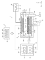
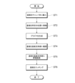
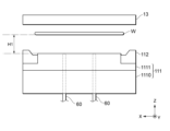
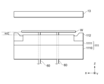
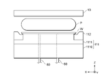
- a plasma processing apparatus includes a chamber, a substrate support provided in the chamber and configured to support a substrate, a plasma generator generating plasma in the chamber, and a substrate support and a substrate in the chamber. and a controller, wherein the controller causes the lifter to move the substrate from a position away from the substrate support toward the substrate support, and during the movement of the substrate, the plasma generator generates plasma in the chamber, and controls the lifter to place the substrate on the substrate support while the plasma is generated in the chamber.
Landscapes
- Physics & Mathematics (AREA)
- Engineering & Computer Science (AREA)
- Plasma & Fusion (AREA)
- Chemical & Material Sciences (AREA)
- Analytical Chemistry (AREA)
- Electromagnetism (AREA)
- Spectroscopy & Molecular Physics (AREA)
- Plasma Technology (AREA)
- Drying Of Semiconductors (AREA)
- Chemical Vapour Deposition (AREA)
Priority Applications (4)
| Application Number | Priority Date | Filing Date | Title |
|---|---|---|---|
| CN202280060608.6A CN117916863A (zh) | 2021-09-14 | 2022-09-12 | 等离子体处理装置和等离子体处理方法 |
| KR1020247011722A KR20240065117A (ko) | 2021-09-14 | 2022-09-12 | 플라스마 처리 장치 및 플라스마 처리 방법 |
| JP2023548462A JPWO2023042804A1 (cg-RX-API-DMAC7.html) | 2021-09-14 | 2022-09-12 | |
| US18/605,369 US12700576B2 (en) | 2021-09-14 | 2024-03-14 | Plasma processing apparatus and plasma processing method |
Applications Claiming Priority (2)
| Application Number | Priority Date | Filing Date | Title |
|---|---|---|---|
| JP2021-149137 | 2021-09-14 | ||
| JP2021149137 | 2021-09-14 |
Related Child Applications (1)
| Application Number | Title | Priority Date | Filing Date |
|---|---|---|---|
| US18/605,369 Continuation US12700576B2 (en) | 2021-09-14 | 2024-03-14 | Plasma processing apparatus and plasma processing method |
Publications (1)
| Publication Number | Publication Date |
|---|---|
| WO2023042804A1 true WO2023042804A1 (ja) | 2023-03-23 |
Family
ID=85602910
Family Applications (1)
| Application Number | Title | Priority Date | Filing Date |
|---|---|---|---|
| PCT/JP2022/034085 Ceased WO2023042804A1 (ja) | 2021-09-14 | 2022-09-12 | プラズマ処理装置及びプラズマ処理方法 |
Country Status (6)
| Country | Link |
|---|---|
| US (1) | US12700576B2 (cg-RX-API-DMAC7.html) |
| JP (1) | JPWO2023042804A1 (cg-RX-API-DMAC7.html) |
| KR (1) | KR20240065117A (cg-RX-API-DMAC7.html) |
| CN (1) | CN117916863A (cg-RX-API-DMAC7.html) |
| TW (1) | TWI923837B (cg-RX-API-DMAC7.html) |
| WO (1) | WO2023042804A1 (cg-RX-API-DMAC7.html) |
Families Citing this family (1)
| Publication number | Priority date | Publication date | Assignee | Title |
|---|---|---|---|---|
| JPWO2023042804A1 (cg-RX-API-DMAC7.html) * | 2021-09-14 | 2023-03-23 |
Citations (4)
| Publication number | Priority date | Publication date | Assignee | Title |
|---|---|---|---|---|
| US20070054504A1 (en) * | 2005-09-07 | 2007-03-08 | Applied Materials, Inc. | Post deposition plasma treatment to increase tensile stress of HDP-CVD SIO2 |
| JP2007220926A (ja) * | 2006-02-17 | 2007-08-30 | Mitsubishi Heavy Ind Ltd | プラズマ処理装置及びプラズマ処理方法 |
| JP2009302285A (ja) * | 2008-06-13 | 2009-12-24 | Shibaura Mechatronics Corp | プラズマ処理装置、プラズマ処理方法、および電子デバイスの製造方法 |
| KR20150131895A (ko) * | 2014-05-16 | 2015-11-25 | 박영소 | 웨이퍼 범프 리플로우 방법 및 장비 |
Family Cites Families (18)
| Publication number | Priority date | Publication date | Assignee | Title |
|---|---|---|---|---|
| US6296735B1 (en) | 1993-05-03 | 2001-10-02 | Unaxis Balzers Aktiengesellschaft | Plasma treatment apparatus and method for operation same |
| US20030000647A1 (en) * | 2001-06-29 | 2003-01-02 | Applied Materials, Inc. | Substrate processing chamber |
| JP6141144B2 (ja) * | 2012-10-02 | 2017-06-07 | 東京エレクトロン株式会社 | 基板処理方法、プログラム、コンピュータ記憶媒体及び基板処理システム |
| US10658222B2 (en) * | 2015-01-16 | 2020-05-19 | Lam Research Corporation | Moveable edge coupling ring for edge process control during semiconductor wafer processing |
| JP7134104B2 (ja) * | 2019-01-09 | 2022-09-09 | 東京エレクトロン株式会社 | プラズマ処理装置およびプラズマ処理装置の載置台 |
| JP2020149859A (ja) | 2019-03-13 | 2020-09-17 | 東京エレクトロン株式会社 | プラズマ処理装置 |
| JP7442349B2 (ja) * | 2020-03-09 | 2024-03-04 | 東京エレクトロン株式会社 | 基板搬送システムおよびロードロックモジュール |
| JP7455012B2 (ja) * | 2020-07-07 | 2024-03-25 | 東京エレクトロン株式会社 | プラズマ処理装置およびプラズマ処理装置の載置台 |
| JP7482746B2 (ja) * | 2020-10-19 | 2024-05-14 | 東京エレクトロン株式会社 | 基板処理装置、基板処理システム、及びメンテナンス方法 |
| KR102580583B1 (ko) * | 2021-08-10 | 2023-09-21 | 피에스케이 주식회사 | 기판 처리 장치 |
| JPWO2023042804A1 (cg-RX-API-DMAC7.html) * | 2021-09-14 | 2023-03-23 | ||
| JP7715467B2 (ja) * | 2022-05-26 | 2025-07-30 | 東京エレクトロン株式会社 | 基板処理装置及びリング部材の位置合わせ方法 |
| KR20250084933A (ko) * | 2022-09-30 | 2025-06-11 | 도쿄엘렉트론가부시키가이샤 | 기판 처리 시스템 |
| KR102760072B1 (ko) * | 2022-10-07 | 2025-01-24 | 도쿄엘렉트론가부시키가이샤 | 기판 처리 시스템 및 엣지 링의 장착 방법 |
| JPWO2024095840A1 (cg-RX-API-DMAC7.html) * | 2022-10-31 | 2024-05-10 | ||
| KR102916370B1 (ko) * | 2023-09-29 | 2026-01-23 | 도쿄엘렉트론가부시키가이샤 | 플라스마 처리 장치 및 플라스마 처리 방법 |
| KR20260065588A (ko) * | 2023-09-29 | 2026-05-08 | 도쿄엘렉트론가부시키가이샤 | 플라스마 처리 장치 및 기판 처리 시스템 |
| CN222320176U (zh) * | 2023-12-21 | 2025-01-07 | 中微半导体设备(上海)股份有限公司 | 一种等离子体处理设备 |
-
2022
- 2022-09-12 JP JP2023548462A patent/JPWO2023042804A1/ja active Pending
- 2022-09-12 WO PCT/JP2022/034085 patent/WO2023042804A1/ja not_active Ceased
- 2022-09-12 KR KR1020247011722A patent/KR20240065117A/ko active Pending
- 2022-09-12 CN CN202280060608.6A patent/CN117916863A/zh active Pending
- 2022-09-14 TW TW111134654A patent/TWI923837B/zh active
-
2024
- 2024-03-14 US US18/605,369 patent/US12700576B2/en active Active
Patent Citations (4)
| Publication number | Priority date | Publication date | Assignee | Title |
|---|---|---|---|---|
| US20070054504A1 (en) * | 2005-09-07 | 2007-03-08 | Applied Materials, Inc. | Post deposition plasma treatment to increase tensile stress of HDP-CVD SIO2 |
| JP2007220926A (ja) * | 2006-02-17 | 2007-08-30 | Mitsubishi Heavy Ind Ltd | プラズマ処理装置及びプラズマ処理方法 |
| JP2009302285A (ja) * | 2008-06-13 | 2009-12-24 | Shibaura Mechatronics Corp | プラズマ処理装置、プラズマ処理方法、および電子デバイスの製造方法 |
| KR20150131895A (ko) * | 2014-05-16 | 2015-11-25 | 박영소 | 웨이퍼 범프 리플로우 방법 및 장비 |
Also Published As
| Publication number | Publication date |
|---|---|
| US12700576B2 (en) | 2026-08-04 |
| TW202331918A (zh) | 2023-08-01 |
| CN117916863A (zh) | 2024-04-19 |
| US20240222095A1 (en) | 2024-07-04 |
| KR20240065117A (ko) | 2024-05-14 |
| JPWO2023042804A1 (cg-RX-API-DMAC7.html) | 2023-03-23 |
| TWI923837B (zh) | 2026-05-01 |
Similar Documents
| Publication | Publication Date | Title |
|---|---|---|
| CN102208322B (zh) | 等离子体处理装置和半导体装置的制造方法 | |
| US8440050B2 (en) | Plasma processing apparatus and method, and storage medium | |
| CN108987233B (zh) | 等离子体处理装置和静电吸附方法 | |
| CN109509694B (zh) | 等离子体处理装置和等离子体处理方法 | |
| US10553409B2 (en) | Method of cleaning plasma processing apparatus | |
| JP2010040627A (ja) | プラズマ処理方法及びプラズマ処理装置 | |
| TWI897949B (zh) | 電漿處理裝置及電漿處理方法 | |
| KR102851000B1 (ko) | 에지링의 지지 방법, 플라즈마 처리 장치, 및 기판 처리 시스템 | |
| US20250191877A1 (en) | Plasma processing apparatus and plasma processing method | |
| CN112490103B (zh) | 静电吸附方法和等离子体处理装置 | |
| TW202539303A (zh) | 電漿處理方法及電漿處理裝置 | |
| CN100570818C (zh) | 等离子体处理装置 | |
| US20250226181A1 (en) | Plasma processing apparatus and power supply system | |
| US20240222095A1 (en) | Plasma processing apparatus and plasma processing method | |
| US11664198B2 (en) | Plasma processing apparatus | |
| JP2023004431A (ja) | プラズマ処理装置 | |
| US12482640B2 (en) | Cleaning method, substrate processing method and plasma processing apparatus | |
| CN120380583A (zh) | 等离子体处理装置和控制方法 | |
| US20240347325A1 (en) | Plasma processing apparatus | |
| JP2025024972A (ja) | 基板処理方法及び基板処理装置 | |
| JP2024098708A (ja) | プラズマ処理装置 | |
| US20240339303A1 (en) | Substrate support and plasma processing apparatus | |
| JP2024092751A (ja) | 基板保持方法および基板処理システム | |
| JP2025090149A (ja) | プラズマ処理方法及びプラズマ処理装置 | |
| JP2025034857A (ja) | 基板処理装置およびクリーニング方法 |
Legal Events
| Date | Code | Title | Description |
|---|---|---|---|
| 121 | Ep: the epo has been informed by wipo that ep was designated in this application |
Ref document number: 22869951 Country of ref document: EP Kind code of ref document: A1 |
|
| WWE | Wipo information: entry into national phase |
Ref document number: 2023548462 Country of ref document: JP |
|
| WWE | Wipo information: entry into national phase |
Ref document number: 202280060608.6 Country of ref document: CN |
|
| ENP | Entry into the national phase |
Ref document number: 20247011722 Country of ref document: KR Kind code of ref document: A |
|
| NENP | Non-entry into the national phase |
Ref country code: DE |
|
| 122 | Ep: pct application non-entry in european phase |
Ref document number: 22869951 Country of ref document: EP Kind code of ref document: A1 |