WO2023042615A1 - 半導体装置、および半導体素子の実装構造 - Google Patents
半導体装置、および半導体素子の実装構造 Download PDFInfo
- Publication number
- WO2023042615A1 WO2023042615A1 PCT/JP2022/031725 JP2022031725W WO2023042615A1 WO 2023042615 A1 WO2023042615 A1 WO 2023042615A1 JP 2022031725 W JP2022031725 W JP 2022031725W WO 2023042615 A1 WO2023042615 A1 WO 2023042615A1
- Authority
- WO
- WIPO (PCT)
- Prior art keywords
- wiring
- electrode
- thickness direction
- semiconductor device
- main surface
- Prior art date
- Legal status (The legal status is an assumption and is not a legal conclusion. Google has not performed a legal analysis and makes no representation as to the accuracy of the status listed.)
- Ceased
Links
Images


Classifications
-
- H—ELECTRICITY
- H10—SEMICONDUCTOR DEVICES; ELECTRIC SOLID-STATE DEVICES NOT OTHERWISE PROVIDED FOR
- H10W—GENERIC PACKAGES, INTERCONNECTIONS, CONNECTORS OR OTHER CONSTRUCTIONAL DETAILS OF DEVICES COVERED BY CLASS H10
- H10W74/00—Encapsulations, e.g. protective coatings
-
- H—ELECTRICITY
- H10—SEMICONDUCTOR DEVICES; ELECTRIC SOLID-STATE DEVICES NOT OTHERWISE PROVIDED FOR
- H10D—INORGANIC ELECTRIC SEMICONDUCTOR DEVICES
- H10D30/00—Field-effect transistors [FET]
- H10D30/40—FETs having zero-dimensional [0D], one-dimensional [1D] or two-dimensional [2D] charge carrier gas channels
- H10D30/47—FETs having zero-dimensional [0D], one-dimensional [1D] or two-dimensional [2D] charge carrier gas channels having two-dimensional [2D] charge carrier gas channels, e.g. nanoribbon FETs or high electron mobility transistors [HEMT]
-
- H—ELECTRICITY
- H10—SEMICONDUCTOR DEVICES; ELECTRIC SOLID-STATE DEVICES NOT OTHERWISE PROVIDED FOR
- H10D—INORGANIC ELECTRIC SEMICONDUCTOR DEVICES
- H10D64/00—Electrodes of devices having potential barriers
- H10D64/20—Electrodes characterised by their shapes, relative sizes or dispositions
- H10D64/23—Electrodes carrying the current to be rectified, amplified, oscillated or switched, e.g. sources, drains, anodes or cathodes
- H10D64/251—Source or drain electrodes for field-effect devices
-
- H—ELECTRICITY
- H10—SEMICONDUCTOR DEVICES; ELECTRIC SOLID-STATE DEVICES NOT OTHERWISE PROVIDED FOR
- H10W—GENERIC PACKAGES, INTERCONNECTIONS, CONNECTORS OR OTHER CONSTRUCTIONAL DETAILS OF DEVICES COVERED BY CLASS H10
- H10W42/00—Arrangements for protection of devices
- H10W42/60—Arrangements for protection of devices protecting against electrostatic charges or discharges, e.g. Faraday shields
-
- H—ELECTRICITY
- H10—SEMICONDUCTOR DEVICES; ELECTRIC SOLID-STATE DEVICES NOT OTHERWISE PROVIDED FOR
- H10W—GENERIC PACKAGES, INTERCONNECTIONS, CONNECTORS OR OTHER CONSTRUCTIONAL DETAILS OF DEVICES COVERED BY CLASS H10
- H10W70/00—Package substrates; Interposers; Redistribution layers [RDL]
- H10W70/60—Insulating or insulated package substrates; Interposers; Redistribution layers
- H10W70/611—Insulating or insulated package substrates; Interposers; Redistribution layers for connecting multiple chips together
-
- H—ELECTRICITY
- H10—SEMICONDUCTOR DEVICES; ELECTRIC SOLID-STATE DEVICES NOT OTHERWISE PROVIDED FOR
- H10W—GENERIC PACKAGES, INTERCONNECTIONS, CONNECTORS OR OTHER CONSTRUCTIONAL DETAILS OF DEVICES COVERED BY CLASS H10
- H10W70/00—Package substrates; Interposers; Redistribution layers [RDL]
- H10W70/60—Insulating or insulated package substrates; Interposers; Redistribution layers
- H10W70/62—Insulating or insulated package substrates; Interposers; Redistribution layers characterised by their interconnections
- H10W70/65—Shapes or dispositions of interconnections
- H10W70/658—Shapes or dispositions of interconnections for devices provided for in groups H10D8/00 - H10D48/00
-
- H—ELECTRICITY
- H10—SEMICONDUCTOR DEVICES; ELECTRIC SOLID-STATE DEVICES NOT OTHERWISE PROVIDED FOR
- H10W—GENERIC PACKAGES, INTERCONNECTIONS, CONNECTORS OR OTHER CONSTRUCTIONAL DETAILS OF DEVICES COVERED BY CLASS H10
- H10W70/00—Package substrates; Interposers; Redistribution layers [RDL]
- H10W70/60—Insulating or insulated package substrates; Interposers; Redistribution layers
- H10W70/67—Insulating or insulated package substrates; Interposers; Redistribution layers characterised by their insulating layers or insulating parts
- H10W70/68—Shapes or dispositions thereof
-
- H—ELECTRICITY
- H10—SEMICONDUCTOR DEVICES; ELECTRIC SOLID-STATE DEVICES NOT OTHERWISE PROVIDED FOR
- H10W—GENERIC PACKAGES, INTERCONNECTIONS, CONNECTORS OR OTHER CONSTRUCTIONAL DETAILS OF DEVICES COVERED BY CLASS H10
- H10W72/00—Interconnections or connectors in packages
-
- H—ELECTRICITY
- H10—SEMICONDUCTOR DEVICES; ELECTRIC SOLID-STATE DEVICES NOT OTHERWISE PROVIDED FOR
- H10W—GENERIC PACKAGES, INTERCONNECTIONS, CONNECTORS OR OTHER CONSTRUCTIONAL DETAILS OF DEVICES COVERED BY CLASS H10
- H10W72/00—Interconnections or connectors in packages
- H10W72/071—Connecting or disconnecting
-
- H—ELECTRICITY
- H10—SEMICONDUCTOR DEVICES; ELECTRIC SOLID-STATE DEVICES NOT OTHERWISE PROVIDED FOR
- H10W—GENERIC PACKAGES, INTERCONNECTIONS, CONNECTORS OR OTHER CONSTRUCTIONAL DETAILS OF DEVICES COVERED BY CLASS H10
- H10W72/00—Interconnections or connectors in packages
- H10W72/20—Bump connectors, e.g. solder bumps or copper pillars; Dummy bumps; Thermal bumps
-
- H—ELECTRICITY
- H10—SEMICONDUCTOR DEVICES; ELECTRIC SOLID-STATE DEVICES NOT OTHERWISE PROVIDED FOR
- H10W—GENERIC PACKAGES, INTERCONNECTIONS, CONNECTORS OR OTHER CONSTRUCTIONAL DETAILS OF DEVICES COVERED BY CLASS H10
- H10W74/00—Encapsulations, e.g. protective coatings
- H10W74/10—Encapsulations, e.g. protective coatings characterised by their shape or disposition
- H10W74/111—Encapsulations, e.g. protective coatings characterised by their shape or disposition the semiconductor body being completely enclosed
- H10W74/114—Encapsulations, e.g. protective coatings characterised by their shape or disposition the semiconductor body being completely enclosed by a substrate and the encapsulations
-
- H—ELECTRICITY
- H10—SEMICONDUCTOR DEVICES; ELECTRIC SOLID-STATE DEVICES NOT OTHERWISE PROVIDED FOR
- H10W—GENERIC PACKAGES, INTERCONNECTIONS, CONNECTORS OR OTHER CONSTRUCTIONAL DETAILS OF DEVICES COVERED BY CLASS H10
- H10W90/00—Package configurations
-
- H—ELECTRICITY
- H10—SEMICONDUCTOR DEVICES; ELECTRIC SOLID-STATE DEVICES NOT OTHERWISE PROVIDED FOR
- H10W—GENERIC PACKAGES, INTERCONNECTIONS, CONNECTORS OR OTHER CONSTRUCTIONAL DETAILS OF DEVICES COVERED BY CLASS H10
- H10W72/00—Interconnections or connectors in packages
- H10W72/20—Bump connectors, e.g. solder bumps or copper pillars; Dummy bumps; Thermal bumps
- H10W72/251—Materials
- H10W72/252—Materials comprising solid metals or solid metalloids, e.g. PbSn, Ag or Cu
-
- H—ELECTRICITY
- H10—SEMICONDUCTOR DEVICES; ELECTRIC SOLID-STATE DEVICES NOT OTHERWISE PROVIDED FOR
- H10W—GENERIC PACKAGES, INTERCONNECTIONS, CONNECTORS OR OTHER CONSTRUCTIONAL DETAILS OF DEVICES COVERED BY CLASS H10
- H10W72/00—Interconnections or connectors in packages
- H10W72/20—Bump connectors, e.g. solder bumps or copper pillars; Dummy bumps; Thermal bumps
- H10W72/251—Materials
- H10W72/255—Materials of outermost layers of multilayered bumps, e.g. material of a coating
-
- H—ELECTRICITY
- H10—SEMICONDUCTOR DEVICES; ELECTRIC SOLID-STATE DEVICES NOT OTHERWISE PROVIDED FOR
- H10W—GENERIC PACKAGES, INTERCONNECTIONS, CONNECTORS OR OTHER CONSTRUCTIONAL DETAILS OF DEVICES COVERED BY CLASS H10
- H10W72/00—Interconnections or connectors in packages
- H10W72/20—Bump connectors, e.g. solder bumps or copper pillars; Dummy bumps; Thermal bumps
- H10W72/281—Auxiliary members
- H10W72/287—Flow barriers
-
- H—ELECTRICITY
- H10—SEMICONDUCTOR DEVICES; ELECTRIC SOLID-STATE DEVICES NOT OTHERWISE PROVIDED FOR
- H10W—GENERIC PACKAGES, INTERCONNECTIONS, CONNECTORS OR OTHER CONSTRUCTIONAL DETAILS OF DEVICES COVERED BY CLASS H10
- H10W74/00—Encapsulations, e.g. protective coatings
- H10W74/10—Encapsulations, e.g. protective coatings characterised by their shape or disposition
- H10W74/111—Encapsulations, e.g. protective coatings characterised by their shape or disposition the semiconductor body being completely enclosed
- H10W74/127—Encapsulations, e.g. protective coatings characterised by their shape or disposition the semiconductor body being completely enclosed characterised by arrangements for sealing or adhesion
-
- H—ELECTRICITY
- H10—SEMICONDUCTOR DEVICES; ELECTRIC SOLID-STATE DEVICES NOT OTHERWISE PROVIDED FOR
- H10W—GENERIC PACKAGES, INTERCONNECTIONS, CONNECTORS OR OTHER CONSTRUCTIONAL DETAILS OF DEVICES COVERED BY CLASS H10
- H10W74/00—Encapsulations, e.g. protective coatings
- H10W74/10—Encapsulations, e.g. protective coatings characterised by their shape or disposition
- H10W74/131—Encapsulations, e.g. protective coatings characterised by their shape or disposition the semiconductor body being only partially enclosed
- H10W74/142—Encapsulations, e.g. protective coatings characterised by their shape or disposition the semiconductor body being only partially enclosed the encapsulations exposing the passive side of the semiconductor body
-
- H—ELECTRICITY
- H10—SEMICONDUCTOR DEVICES; ELECTRIC SOLID-STATE DEVICES NOT OTHERWISE PROVIDED FOR
- H10W—GENERIC PACKAGES, INTERCONNECTIONS, CONNECTORS OR OTHER CONSTRUCTIONAL DETAILS OF DEVICES COVERED BY CLASS H10
- H10W90/00—Package configurations
- H10W90/701—Package configurations characterised by the relative positions of pads or connectors relative to package parts
- H10W90/721—Package configurations characterised by the relative positions of pads or connectors relative to package parts of bump connectors
- H10W90/724—Package configurations characterised by the relative positions of pads or connectors relative to package parts of bump connectors between a chip and a stacked insulating package substrate, interposer or RDL
Definitions
- the present disclosure relates to a semiconductor device including a flip-mounted semiconductor element and a mounting structure for the semiconductor element.
- Patent Literature 1 discloses an example of a semiconductor device including a semiconductor element (HEMT) with a horizontal structure.
- a semiconductor element has a first electrode and a second electrode.
- the semiconductor element is mounted on the die pad.
- the first electrode and the second electrode are electrically connected to a plurality of terminal leads located around the die pad via wires.
- the semiconductor element shown in Patent Document 1 may be flip-chip mounted on a wiring board or the like.
- the distance between the first electrode and the second electrode may be shortened in order to reduce the size of the semiconductor element.
- the distance between the first electrode and the second electrode is shortened, the distance between the wirings to which the semiconductor elements are electrically connected becomes smaller.
- the withstand voltage of the wiring board or the like on which the semiconductor element is mounted is lowered. Therefore, even when miniaturization of a semiconductor device is attempted, a measure for suppressing a decrease in withstand voltage of a wiring board or the like is desired.
- one object of the present disclosure is to provide a semiconductor device capable of suppressing a decrease in dielectric breakdown voltage while miniaturizing the semiconductor element, and a mounting structure of the semiconductor element.
- a semiconductor device provided by a first aspect of the present disclosure includes a substrate having a main surface facing a thickness direction, first wiring and second wiring provided on the main surface, and facing the main surface. and a second electrode facing the main surface and positioned next to the first electrode.
- the first electrode is electrically connected to the first wiring
- the second electrode is electrically connected to the second wiring.
- the substrate includes a first portion, a second portion, and a third portion, and the first portion includes a portion of the main surface and includes the first wiring and the first electrode when viewed in the thickness direction. overlaps with The second portion includes part of the main surface and overlaps the second wiring and the second electrode when viewed in the thickness direction.
- the third portion is positioned between the first portion and the second portion when viewed in the thickness direction.
- the third portion has a first surface, and a normal direction of the first surface intersects the thickness direction.
- a semiconductor device mounting structure provided by a second aspect of the present disclosure includes a substrate having a main surface facing a thickness direction, and first wiring and second wiring provided on the main surface.
- a semiconductor element having a wiring substrate, a first electrode facing the main surface, and a second electrode facing the main surface and positioned next to the first electrode.
- the first electrode is electrically connected to the first wiring
- the second electrode is electrically connected to the second wiring.
- the substrate includes a first portion, a second portion, and a third portion, and the first portion includes a portion of the main surface and includes the first wiring and the first electrode when viewed in the thickness direction. overlaps with The second portion includes part of the main surface and overlaps the second wiring and the second electrode when viewed in the thickness direction.
- the third portion is positioned between the first portion and the second portion when viewed in the thickness direction.
- the third portion has a first surface, and a normal direction of the first surface intersects the thickness direction.
- the semiconductor device and the mounting structure of the semiconductor element according to the present disclosure it is possible to reduce the size of the semiconductor element while suppressing a decrease in dielectric strength voltage.
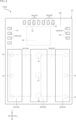
- FIG. 1 is a plan view of a semiconductor device according to a first embodiment of the present disclosure
- FIG. FIG. 2 is a plan view corresponding to FIG. 1 and omits illustration of the sealing resin.
- FIG. 5 is a cross-sectional view along line VV in FIG.
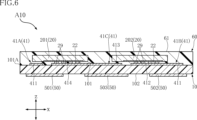
- FIG. 6 is a cross-sectional view taken along line VI-VI of FIG.
- FIG. 7 is a cross-sectional view along line VII-VII of FIG.
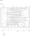
- FIG. 8 is a cross-sectional view along line VIII-VIII of FIG. 9 is a partially enlarged view of FIG. 3.
- FIG. 3 is a plan view corresponding to FIG. 1 and omits illustration of the sealing resin.
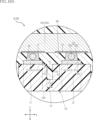
- FIG. 10A is a partially enlarged view of FIG. 8.
- FIG. 10B is a partially enlarged cross-sectional view corresponding to FIG. 10A, showing another configuration of the substrate.
- FIG. 11 is a partially enlarged cross-sectional view of a modification of the semiconductor device shown in FIG.
- FIG. 12 is a cross-sectional view of a semiconductor device according to a second embodiment of the present disclosure; 13 is a partially enlarged view of FIG. 12.
- FIG. FIG. 14 is a cross-sectional view of a semiconductor device according to a third embodiment of the present disclosure; 15 is a partially enlarged view of FIG. 14.
- FIG. 16 is a partially enlarged cross-sectional view of a modification of the semiconductor device shown in FIG. 14.
- FIG. 17 is a plan view of a semiconductor device according to a fourth embodiment of the present disclosure
- FIG. 18 is a cross-sectional view taken along line XVIII-XVIII in FIG. 17.
- FIG. 19 is a cross-sectional view along line XIX-XIX in FIG. 17.
- FIG. 20 is a plan view of a mounting structure of a semiconductor element according to the first embodiment of the present disclosure
- FIG. 21 is a cross-sectional view taken along line XXI-XXI of FIG. 20.
- FIG. 22 is a cross-sectional view along line XXII-XXII of FIG. 20.
- FIG. 23 is a cross-sectional view taken along line XXIII-XXIII of FIG. 20.
- FIG. 24 is a partially enlarged view of FIG. 23.
- FIG. FIG. 25 is a plan view of a semiconductor device mounting structure according to a second embodiment of the present disclosure; 26 is a cross-sectional view along line XXVI-XXVI of FIG. 25.
- FIG. 25 is a plan view of a semiconductor device mounting structure according to a second embodiment of the present disclosure.
- 26 is a cross-sectional view along line XXVI-XXVI of FIG. 25.
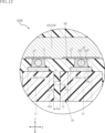
- the semiconductor device A10 includes a substrate 10, a semiconductor element 20, a bonding layer 29, an IC 30, a plurality of wirings 41, a plurality of interconnecting wirings 42, a plurality of terminals 50, and a sealing resin 60.
- the semiconductor device A10 is of a resin package type that is surface-mounted on a wiring board.
- the semiconductor device A10 converts DC power supplied to the semiconductor device A10 from the outside into AC power by the semiconductor element 20 .
- the converted AC power is supplied to an object to be driven such as a motor.
- FIG. 2 omits illustration of the sealing resin 60 for convenience of understanding.
- FIG. 3 shows the semiconductor element 20 and the IC 30 transparently with respect to FIG. In FIG. 3, the transmitted semiconductor element 20 and IC 30 are indicated by an imaginary line (double-dot chain line).
- the thickness direction of the substrate 10 is called "thickness direction z" for convenience.
- a direction perpendicular to the thickness direction z is called a “first direction x”.
- a direction orthogonal to both the thickness direction z and the first direction x is called a "second direction y”.
- the semiconductor device A10 has a rectangular shape when viewed in the thickness direction z.
- the substrate 10 supports a plurality of wirings 41, a plurality of connecting wirings 42 and a plurality of terminals 50, as shown in FIGS.
- the substrate 10 has electrical insulation.
- the substrate 10 is made of a material containing resin.
- An example of the resin is an epoxy resin.
- the substrate 10 has a main surface 101 and a back surface 102.
- the main surface 101 faces the thickness direction z.
- the back surface 102 faces the opposite side in the thickness direction z.
- the back surface 102 is exposed to the outside of the semiconductor device A10.
- the rear surface 102 faces the wiring board.
- the semiconductor element 20 faces the main surface 101 of the substrate 10, as shown in FIGS.
- the semiconductor element 20 is a transistor (switching element) mainly used for power conversion.
- the semiconductor element 20 is made of a material containing a nitride semiconductor.
- the semiconductor element 20 is a HEMT (High Electron Mobility Transistor) made of a material containing gallium nitride (GaN).
- Semiconductor device 20 includes a first device 201 and a second device 202 . The first element 201 and the second element 202 are positioned apart from each other in the first direction x.
- the semiconductor element 20 has a plurality of first electrodes 21, a plurality of second electrodes 22, and two third electrodes .
- a plurality of first electrodes 21 , a plurality of second electrodes 22 and two third electrodes 23 face main surface 101 of substrate 10 .
- the plurality of first electrodes 21 and the plurality of second electrodes 22 extend in the second direction y.
- the plurality of first electrodes 21 and the plurality of second electrodes 22 are arranged alternately along the first direction x.
- a current corresponding to power before being converted by the semiconductor element 20 flows through the plurality of first electrodes 21 . Therefore, the multiple first electrodes 21 correspond to the drain of the semiconductor element 20 .
- a current corresponding to the power converted by the semiconductor element 20 flows through the plurality of second electrodes 22 . Therefore, the multiple second electrodes 22 correspond to the source of the semiconductor element 20 .
- the two third electrodes 23 are located on both sides of the semiconductor element 20 in the second direction y.
- a gate voltage for driving the semiconductor element 20 is applied to one of the two third electrodes 23 .
- the area of the two third electrodes 23 is smaller than the area of each of the plurality of first electrodes 21 and the plurality of second electrodes 22 .
- the shape and arrangement of the plurality of first electrodes 21, the plurality of second electrodes 22, and the two third electrodes 23 in the semiconductor element 20 are examples, and are not limited to these.
- the IC 30 faces the main surface 101 of the substrate 10, as shown in FIGS.
- the IC 30 is a gate driver that applies a gate voltage to the third electrode 23 of the semiconductor element 20 (the first element 201 and the second element 202).
- IC 30 has a plurality of electrodes 31 .
- a plurality of electrodes 31 face main surface 101 .
- a plurality of wirings 41 are provided on the main surface 101 of the substrate 10, as shown in FIGS.
- a composition of the plurality of wirings 41 includes, for example, copper (Cu).
- the multiple wirings 41 include an input wiring 41A, a ground wiring 41B, an output wiring 41C, a first gate wiring 41D, a second gate wiring 41E, a potential wiring 41F and a plurality of control wirings 41G.
- the input wiring 41A and the ground wiring 41B are positioned apart from each other in the first direction x.
- the input wiring 41A and the ground wiring 41B have a first base portion 411 and a plurality of first extension portions 412 .
- the first base 411 extends in the second direction y.
- the plurality of first extending portions 412 extend in the first direction x from the first base portion 411 toward the second base portion 413 of the output wiring 41C, which will be described later.
- the multiple first extensions 412 are arranged along the second direction y.
- the plurality of first electrodes 21 of the first element 201 are individually conductively joined to the plurality of first extending portions 412 of the input wiring 41A via the joining layer 29 .
- the plurality of second electrodes 22 of the second element 202 are electrically connected to the plurality of first extending portions 412 of the ground wiring 41B via the bonding layer 29 .
- the composition of the bonding layer 29 contains tin (Sn).
- bonding layer 29 has metal core 291 and metal layer 292 .
- a metal layer 292 covers the metal core 291 .
- the composition of the metal core 291 contains nickel (Ni).
- the composition of metal layer 292 includes tin.
- the bonding layer 29 is a so-called solder ball.
- the output wiring 41C is located between the first base 411 of the input wiring 41A and the first base 411 of the ground wiring 41B in the first direction x.
- the output wiring 41 ⁇ /b>C has a second base portion 413 and a plurality of second extension portions 414 .
- the second base 413 extends in the second direction y.
- the plurality of second extensions 414 extend in the first direction x from both sides of the second base 413 in the first direction x toward the first base 411 of the input wiring 41A and the first base 411 of the ground wiring 41B. there is The plurality of second extensions 414 are arranged along the second direction y.
- the plurality of second electrodes 22 of the first element 201 are individually conductively joined to the plurality of second extension portions 414 of the output wiring 41C via the joining layer 29 .
- the plurality of first electrodes 21 of the second element 202 are individually conductively joined to the plurality of second extending portions 414 of the output wiring 41C via the joining layer 29 .
- the plurality of first electrodes 21 of the second element 202 are electrically connected to the plurality of second electrodes 22 of the first element 201 .
- one of the two third electrodes 23 of the first element 201 is electrically connected to the first gate wiring 41D via the bonding layer 29.
- one of the two third electrodes 23 of the second element 202 is electrically connected to the second gate wiring 41E via the bonding layer 29.
- FIG. 8 one of the two third electrodes 23 of the first element 201 is electrically connected to the first gate wiring 41D via the bonding layer 29.
- FIG. 2 one of the two third electrodes 23 of the second element 202 is electrically connected to the second gate wiring 41E via the bonding layer 29.
- the potential wiring 41F is connected to the second base portion 413 of the output wiring 41C.
- the potential wiring 41 ⁇ /b>F is used when setting the ground of the gate voltage applied to the third electrode 23 of the first element 201 by the IC 30 .
- the plurality of electrodes 31 of the IC 30 are individually conductively connected to the first gate wiring 41D, the second gate wiring 41E, the potential wiring 41F and the plurality of control wirings 41G. . Accordingly, the IC 30 is electrically connected to the third electrode 23 of the first element 201, the third electrode 23 of the second element 202, and the output wiring 41C.
- the substrate 10 includes a plurality of first parts 11, a plurality of second parts 12 and a plurality of third parts 13. As shown in FIG. The plurality of first portions 11 , the plurality of second portions 12 and the plurality of third portions 13 overlap the semiconductor element 20 when viewed in the thickness direction z. In the subsequent description of the plurality of first parts 11, the plurality of second parts 12, and the plurality of third parts 13, the plurality of first parts 11 and the plurality of second parts overlapping the first elements 201 of the semiconductor element 20 12 and a plurality of third parts 13.
- the plurality of first parts 11 includes part of the major surface 101 of the substrate 10. As shown in FIG. When viewed in the thickness direction z, each of the plurality of first portions 11 overlaps one of the plurality of first electrodes 21 of the first element 201 and one of the plurality of first extending portions 412 of the input wiring 41A. ing. In FIG. 9, regions corresponding to the plurality of first portions 11 are indicated by a plurality of oblique lines.
- the plurality of second parts 12 includes part of the main surface 101 of the substrate 10. As shown in FIGS. When viewed in the thickness direction z, each of the plurality of second portions 12 overlaps one of the plurality of second electrodes 22 of the first element 201 and one of the plurality of second extensions 414 of the output wiring 41C. ing. In FIG. 9, regions corresponding to the plurality of second portions 12 are indicated by a plurality of oblique lines.
- each of the plurality of third portions 13 is formed between one of the plurality of first portions 11 and one of the plurality of second portions 12 positioned next to it when viewed in the thickness direction z. located in between.
- the multiple third portions 13 extend in a direction orthogonal to the thickness direction z.
- the plurality of third portions 13 are positioned away from the peripheral edge 101A of the main surface 101 of the substrate 10 .
- the plurality of third parts 13 includes first ends 13A and second ends 13B.
- the first end 13A and the second end 13B are positioned on both sides in the direction in which the plurality of third portions 13 extend.
- the first end 13A is located between the first edge 412A of the plurality of first extensions 412 of the input wiring 41A and the second base 413 of the output wiring 41C.
- the second end 13B is positioned between the first base portion 411 of the input wiring 41A and the second edges 414A of the plurality of second extensions 414 of the output wiring 41C.
- the multiple third parts 13 have a first surface 131 and a second surface 132 .
- the normal direction m of the first surface 131 intersects the thickness direction z.
- the normal direction m is orthogonal to the thickness direction z. Therefore, the inclination angle ⁇ of the first surface 131 with respect to the main surface 101 of the substrate 10 is 90°.
- the first surface 131 is connected to the principal surface 101 .
- the first surface 131 includes a pair of regions spaced apart from each other. The direction in which the pair of regions separate is the same as the direction in which the first electrode 21 and the second electrode 22 of the first element 201 separate from each other.
- the second surface 132 faces the same side as the main surface 101 in the thickness direction z.
- the second surface 132 is connected to the first surface 131 .
- the first surface 131 and the second surface 132 of the plurality of third portions 13 are arranged on the opposite side of the first element 201 with the main surface 101 of the substrate 10 interposed therebetween in the thickness direction z.
- the plurality of third portions 13 are defined by the first surface 131 and the second surface 132 and have grooves recessed from the main surface 101 .
- a dimension d1 in the thickness direction z of the first surface 131 is larger than a dimension b of the second surface 132 in the direction in which the first electrode 21 and the second electrode 22 of the first element 201 are separated from each other.
- FIG. 10B shows another configuration of the plurality of third parts 13.
- the normal direction m of the first surface 131 intersects the thickness direction z, but is not orthogonal to the thickness direction z.
- the inclination angle ⁇ of the first surface 131 with respect to the main surface 101 of the substrate 10 is 70° or more and 110° or less.
- a more preferable angle of inclination ⁇ is 80° or more and 100° or less.
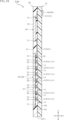
- a plurality of interconnecting wirings 42 are embedded in the substrate 10 as shown in FIGS. Both sides of the plurality of connecting wires 42 in the thickness direction z are exposed from the main surface 101 and the back surface 102 of the substrate 10 .
- Each of the plurality of interconnecting wirings 42 is connected to one of the plurality of wirings 41 other than the first gate wiring 41D, the second gate wiring 41E and the first gate wiring 41D.
- each of the plurality of interconnecting wirings 42 is connected to one of the plurality of terminals 50 . Accordingly, each of the plurality of terminals 50 is electrically connected to any one of the plurality of wirings 41, the input wiring 41A, the ground wiring 41B, the output wiring 41C, and the plurality of control wirings 41G.
- the composition of the plurality of interconnecting wirings 42 includes, for example, copper.
- a plurality of terminals 50 are provided on the rear surface 102 of the substrate 10, as shown in FIGS.
- the semiconductor device A10 is mounted on the wiring board by wire-bonding the plurality of terminals 50 to the wiring board via solder.
- the plurality of terminals 50 includes multiple metal layers.
- the plurality of metal layers are laminated in order of a nickel layer and a gold (Au) layer from the side closer to the back surface 102 .
- the plurality of metal layers may be formed by laminating a nickel layer, a palladium (Pd) layer, and a gold layer in this order from the side near the back surface 102 .
- the plurality of terminals 50 includes an input terminal 501 , a ground terminal 502 , an output terminal 503 and a plurality of control terminals 504 .
- the input terminal 501 is electrically connected to the input wiring 41A.
- the ground terminal 502 is electrically connected to the ground wiring 41B. DC power to be converted by the semiconductor device 20 is input to the input terminal 501 and the ground terminal 502 .
- the input terminal 501 is a positive electrode (P terminal).
- the ground terminal 502 is a negative electrode (N terminal).
- the output terminal 503 is electrically connected to the output wiring 41C.
- the AC power converted by the semiconductor element 20 is output to the output terminal 503 .
- a plurality of control terminals 504 are electrically connected to the IC 30 via a plurality of control wirings 41G. Power for driving the IC 30 is input to one of the plurality of control terminals 504 . An electric signal to the IC 30 is input to one of the plurality of control terminals 504 . Furthermore, an electrical signal from the IC 30 is output from one of the plurality of control terminals 504 .
- the sealing resin 60 covers the semiconductor element 20, the IC 30 and the plurality of wirings 41, as shown in FIGS. As shown in FIG. 10A , the sealing resin 60 is in contact with the main surface 101 of the substrate 10 and the first surface 131 and the second surface 132 of the plurality of third portions 13 of the substrate 10 . Therefore, in the semiconductor device A10, a part of the sealing resin 60 enters the grooves forming part of the plurality of third parts 13. As shown in FIG.
- the sealing resin 60 has electrical insulation. Sealing resin 60 is made of a material containing, for example, black epoxy resin. As shown in FIGS. 1 and 5-8, the sealing resin 60 has a top surface 61. As shown in FIG. The top surface 61 faces the same side as the main surface 101 of the substrate 10 in the thickness direction z.
- the configuration of the plurality of third portions 13 of the substrate 10 of the semiconductor device A11 differs from that of the semiconductor device A10.
- the plurality of third portions 13 further has third surfaces 133 and fourth surfaces 134 .
- the third surface 133 faces the same side as the main surface 101 of the substrate 10 in the thickness direction z.
- the fourth surface 134 faces a direction perpendicular to the thickness direction z and is connected to the third surface 133 and main surface 101 .
- the fourth surface 134 includes a pair of regions spaced apart from each other. The direction in which the pair of regions separate is the same as the direction in which the first electrode 21 and the second electrode 22 of the first element 201 separate from each other.
- each of the plurality of third portions 13 is defined by the first surface 131 and the second surface 132, and is defined by the groove recessed from the main surface 101 of the substrate 10, the third surface 133 and the fourth surface 134. , and grooves recessed from the main surface 101 .
- the third surfaces 133 of the plurality of third portions 13 are located between the main surface 101 of the substrate 10 and the second surface 132 in the thickness direction z. Accordingly, in the plurality of third portions 13, the dimension d2 of the fourth surface 134 in the thickness direction z is smaller than the dimension d1 of the first surface 131 in the thickness direction z. Furthermore, the dimension d2 is larger than the dimension of the third surface 133 in the direction in which the first electrode 21 and the second electrode 22 of the first element 201 are separated from each other.
- the substrate 10 of the semiconductor device A10 includes a first part 11, a second part 12 and a third part 13.
- the first portion 11 includes part of the main surface 101 of the substrate 10 and overlaps the wiring 41 and the first electrode 21 of the semiconductor element 20 when viewed in the thickness direction z.
- the second portion 12 includes part of the main surface 101 and overlaps the wiring 41 and the second electrode 22 of the semiconductor element 20 when viewed in the thickness direction z.
- the third portion 13 is positioned between the first portion 11 and the second portion 12 when viewed in the thickness direction z.
- the third portion 13 has a first surface 131, and the normal direction m of the first surface 131 intersects the thickness direction z.
- the normal direction m and the thickness direction z are orthogonal to each other, but the present disclosure is not limited to this.
- the creepage distance of the substrate 10 from the first portion 11 to the second portion 12 increases.
- the first electrode 21 overlaps the first electrode 21 when viewed in the thickness direction z.
- Shortening of the creepage distance of the substrate 10 from the wiring 41 to the wiring 41 overlapping the second electrode 22 is suppressed. Therefore, according to the semiconductor device A10, it is possible to suppress a decrease in the breakdown voltage of the semiconductor device A10 while miniaturizing the semiconductor element 20.
- the third portion 13 of the substrate 10 has a second surface 132 facing the same side as the main surface 101 of the substrate 10 in the thickness direction z.
- the first surface 131 and the second surface 132 of the third portion 13 are located on the opposite side of the semiconductor element 20 with the main surface 101 interposed therebetween in the thickness direction z.
- the third portion 13 includes a groove defined by the first surface 131 and the second surface 132 and recessed from the main surface 101 .
- the dimension d1 in the thickness direction z of the first surface 131 shown in FIG. 10A is larger than the dimension b of the second surface 132 in the direction in which the first electrode 21 and the second electrode 22 of the semiconductor element 20 separate from each other. .
- the molten bonding layer 29 may overflow the wiring 41 if at least a part of the bonding layer 29 contains solder. In this case, the melted bonding layer 29 flows into the groove forming a part of the third portion 13 of the substrate 10, thereby restricting the spreading of the bonding layer 29. As shown in FIG. Therefore, it is possible to prevent the wiring 41 from being short-circuited due to the bonding layer 29 .
- the third portion 13 of the substrate 10 is located away from the peripheral edge 101A of the main surface 101 of the substrate 10 when viewed in the thickness direction z. As a result, the groove forming part of the third portion 13 is closed by the first surface 131 . With this configuration, it is possible to suppress a decrease in the mechanical strength of the substrate 10 .
- the semiconductor device A10 further includes a bonding layer 29 that electrically connects the wiring 41 and the first electrode 21 and the second electrode 22 of the semiconductor element 20 .
- the bonding layer 29 has a metal core 291 and a metal layer 292 covering the metal core 291 .
- the composition of metal layer 292 includes tin.
- the semiconductor device A10 further includes a sealing resin 60 that covers the semiconductor element 20.
- the sealing resin 60 is in contact with the first surface 131 of the third portion 13 of the substrate 10 .
- the sealing resin 60 functions as a reinforcing member for the substrate 10 .
- the semiconductor device A10 further includes terminals 50 provided on the back surface 102 of the substrate 10 and connecting wirings 42 embedded in the substrate 10 .
- the communication wiring 42 is connected to the wiring 41 and the terminal 50 .
- FIG. 12 A semiconductor device A20 according to the second embodiment of the present disclosure will be described based on FIGS. 12 and 13.
- FIG. In these figures, elements that are the same as or similar to those of the semiconductor device A10 described above are denoted by the same reference numerals, and overlapping descriptions are omitted.
- the position in FIG. 12 is the same as the position in FIG. 8 showing the semiconductor device A10.
- the configuration of the plurality of third portions 13 of the substrate 10 is different from that of the semiconductor device A10.
- the first surfaces 131 of the plurality of third parts 13 are connected to the main surface 101 and the back surface 102 of the substrate 10 . Therefore, the plurality of third portions 13 do not have the second surfaces 132 . Thereby, as shown in FIG. 12, the plurality of third portions 13 are defined by the first surface 131 and have a configuration including slits penetrating the substrate 10 in the thickness direction z.
- the substrate 10 of the semiconductor device A20 includes a first part 11, a second part 12 and a third part 13.
- the first portion 11 includes part of the main surface 101 of the substrate 10 and overlaps the wiring 41 and the first electrode 21 of the semiconductor element 20 when viewed in the thickness direction z.
- the second portion 12 includes part of the main surface 101 and overlaps the wiring 41 and the second electrode 22 of the semiconductor element 20 when viewed in the thickness direction z.
- the third portion 13 is positioned between the first portion 11 and the second portion 12 when viewed in the thickness direction z.
- the third portion 13 has a first surface 131, and the normal direction m of the first surface 131 intersects (or is perpendicular to) the thickness direction z.
- the semiconductor device A20 since the semiconductor device A20 has the same configuration as the semiconductor device A10, the semiconductor device A20 also exhibits the effects of the configuration.
- the first surface 131 of the third portion 13 of the substrate 10 is connected to the main surface 101 and the back surface 102.
- the dimension d1 in the thickness direction z of the first surface 131 is larger than the dimension d1 of the first surface 131 of the semiconductor device A10. Therefore, since the creepage distance of the substrate 10 from the first part 11 to the second part 12 is further increased than in the case of the semiconductor device A10, it is possible to more effectively suppress the deterioration of the breakdown voltage of the semiconductor device A20.
- the third portion 13 of the substrate 10 includes a slit defined by the first surface 131 and penetrating the substrate 10 in the thickness direction z.
- the molten bonding layer 29 may overflow the wiring 41 if at least a part of the bonding layer 29 contains solder.
- the melted bonding layer 29 flows into the slit forming a part of the third portion 13 , thereby restricting the spreading of the bonding layer 29 . Therefore, it is possible to prevent the wiring 41 from being short-circuited due to the bonding layer 29 . Due to the difference in the dimension d1 in the thickness direction z of the first surface 131, this operational effect is greater than that of the semiconductor device A10.
- FIG. 14 A semiconductor device A30 according to the third embodiment of the present disclosure will be described based on FIGS. 14 and 15.
- FIG. In these figures, elements that are the same as or similar to those of the semiconductor device A10 described above are denoted by the same reference numerals, and overlapping descriptions are omitted.
- the position in FIG. 14 is the same as the position in FIG. 8 showing the semiconductor device A10.
- the configuration of the plurality of third portions 13 of the substrate 10 is different from that of the semiconductor device A10.
- the first surface 131 and the second surface 132 of the plurality of third parts 13 are located between the main surface 101 of the substrate 10 and the first element 201 in the thickness direction z.
- the second surface 132 is located on the side opposite to the main surface 101 with the first surface 131 interposed therebetween in the thickness direction z.
- the plurality of third portions 13 are defined by the first surface 131 and the second surface 132 and include ridges projecting from the main surface 101 .
- the plurality of third portions 13 includes projections 14 having first surfaces 131 and second surfaces 132 .
- the protrusion 14 is made of a material that is an insulator.
- the protrusion 14 is bonded to the major surface 101 of the substrate 10 via the adhesive layer 19 .
- a protrusion 14 forms a ridge included in each of the plurality of third portions 13 .
- the plurality of third portions 13 may be integrally molded on the substrate 10 together with the plurality of first portions 11 and the plurality of second portions 12 .
- the height h from the main surface 101 of the substrate 10 to the second surfaces 132 of the plurality of third portions 13 is greater than the thickness t of each of the plurality of wirings 41 . Furthermore, the height h is greater than the dimension b of the second surface 132 in the direction in which the first electrode 21 and the second electrode 22 of the first element 201 are separated from each other.
- the configuration of the plurality of third portions 13 of the substrate 10 of the semiconductor device A31 differs from that of the semiconductor device A30.
- the plurality of third portions 13 further has a third surface 133 , a fourth surface 134 and a fifth surface 135 .
- the third surface 133 and the fifth surface 135 face the same side as the major surface 101 of the substrate 10 in the thickness direction z.
- the third surface 133 is located on the opposite side of the second surface 132 with the fifth surface 135 interposed therebetween.
- the third surface 133 is positioned between the second surface 132 and the fifth surface 135 in the thickness direction z.
- the fourth surface 134 faces a direction perpendicular to the thickness direction z and is connected to the third surface 133 .
- each of the first surface 131 and the fourth surface 134 of the plurality of third parts 13 includes two regions located apart from each other. The direction in which these two regions separate is the same as the direction in which the first electrode 21 and the second electrode 22 of the first element 201 separate from each other. One area of the first surface 131 and one area of the fourth surface 134 are connected to the fifth surface 135 . Accordingly, each of the plurality of third portions 13 is defined by the first surface 131, the second surface 132, and the fifth surface 135, and includes a ridge protruding from the main surface 101 of the substrate 10, the third surface 133, ridges defined by the fourth surface 134 and the fifth surface 135 and protruding from the main surface 101 .
- the substrate 10 of the semiconductor device A30 includes a first portion 11, a second portion 12 and a third portion 13.
- the first portion 11 includes part of the main surface 101 of the substrate 10 and overlaps the wiring 41 and the first electrode 21 of the semiconductor element 20 when viewed in the thickness direction z.
- the second portion 12 includes part of the main surface 101 and overlaps the wiring 41 and the second electrode 22 of the semiconductor element 20 when viewed in the thickness direction z.
- the third portion 13 is positioned between the first portion 11 and the second portion 12 when viewed in the thickness direction z.
- the third portion 13 has a first surface 131, and the normal direction m of the first surface 131 intersects (or is perpendicular to) the thickness direction z.
- the semiconductor device A30 since the semiconductor device A30 has the same configuration as the semiconductor device A10, the semiconductor device A30 also exhibits the effects of the configuration.
- the third portion 13 of the substrate 10 includes a ridge defined by the first surface 131 and the second surface 132 and protruding from the main surface 101 of the substrate 10.
- the molten bonding layer 29 may overflow the wiring 41 if at least a part of the bonding layer 29 contains solder.
- the contact of the melted bonding layer 29 with the first surface 131 restricts the spread of the bonding layer 29 . Therefore, it is possible to prevent the wiring 41 from being short-circuited due to the bonding layer 29 .
- the height h from the main surface 101 to the second surface 132 to be larger than the thickness t of each of the plurality of wirings 41 in order to sufficiently exhibit this effect. .
- the third portion 13 of the substrate 10 forms a ridge projecting from the main surface 101 of the substrate 10 .
- the second surface 132 of the third portion 13 contacts the semiconductor element 20 so that the wiring 41 and the first first surface of the semiconductor element 20 are connected. It becomes possible to secure the space between the electrode 21 and the first electrode 21 .
- the third portion 13 of the substrate 10 further has a third surface 133, a fourth surface 134 and a fifth surface 135.
- the creepage distance of the substrate 10 from the first portion 11 to the second portion 12 is further increased than in the case of the semiconductor device A30, so that it is possible to more effectively suppress the deterioration of the breakdown voltage of the semiconductor device A31. .
- FIG. 17 to 19 A semiconductor device A40 according to the fourth embodiment of the present disclosure will be described based on FIGS. 17 to 19.
- FIG. 17 elements that are the same as or similar to those of the semiconductor device A10 described above are denoted by the same reference numerals, and overlapping descriptions are omitted.
- the configurations of the semiconductor element 20 and the IC 30 are different from those of the semiconductor device A10.
- the semiconductor element 20 (the first element 201 and the second element 202) has an exposed surface .
- the exposed surface 24 faces the same side as the major surface 101 of the substrate 10 in the thickness direction z.
- the exposed surface 24 is exposed from the top surface 61 of the sealing resin 60 .
- the exposed surface 24 is flush with the top surface 61 .
- the IC 30 has an exposed surface 32 as shown in FIGS.
- the exposed surface 32 faces the same side as the major surface 101 of the substrate 10 in the thickness direction z.
- the exposed surface 32 is exposed from the top surface 61 of the sealing resin 60 .
- the exposed surface 32 is flush with the top surface 61 . Therefore, the position of the exposed surface 32 is equal to the position of the exposed surface 24 in the thickness direction z.
- the configuration of the plurality of third portions 13 of the substrate 10 shown in FIG. 19 is the same as the configuration of the plurality of third portions 13 of the semiconductor device A10.
- the configuration of the plurality of third portions 13 can be the same as the configuration of the plurality of third portions 13 of the semiconductor device A20 or the same as the configuration of the plurality of third portions 13 of the semiconductor device A30.
- the substrate 10 of the semiconductor device A40 includes a first part 11, a second part 12 and a third part 13.
- the first portion 11 includes part of the main surface 101 of the substrate 10 and overlaps the wiring 41 and the first electrode 21 of the semiconductor element 20 when viewed in the thickness direction z.
- the second portion 12 includes part of the main surface 101 and overlaps the wiring 41 and the second electrode 22 of the semiconductor element 20 when viewed in the thickness direction z.
- the third portion 13 is positioned between the first portion 11 and the second portion 12 when viewed in the thickness direction z.
- the third portion 13 has a first surface 131, and the normal direction m of the first surface 131 intersects (or is perpendicular to) the thickness direction z.
- the semiconductor device A40 since the semiconductor device A40 has the same configuration as the semiconductor device A10, the semiconductor device A40 also exhibits the effects of the configuration.
- the semiconductor element 20 has an exposed surface 24 exposed from the top surface 61 of the sealing resin 60 .
- the heat generated from the semiconductor element 20 can be efficiently released to the outside when the semiconductor device A40 is used.
- the dimension of the sealing resin 60 in the thickness direction z can be made smaller. This contributes to miniaturization of the semiconductor device A40.
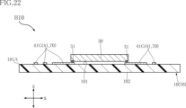
- mounting structure B10 Semiconductor device mounting structure 20 to 24, the semiconductor element mounting structure (hereinafter referred to as "mounting structure B10") according to the first embodiment of the present disclosure will be described.
- elements that are the same as or similar to those of the semiconductor device A10 described above are denoted by the same reference numerals, and overlapping descriptions are omitted.
- the mounting structure B10 includes a wiring board 70, a semiconductor element 20, a bonding layer 29, and an IC30.
- the mounting structure B10 converts DC power supplied to the mounting structure B10 from the outside into AC power by the semiconductor element 20 .
- the converted AC power is supplied to an object to be driven such as a motor.
- the wiring board 70 has the substrate 10 and a plurality of wirings 41.
- the input wiring 41A and the ground wiring 41B are electrically connected to a DC power supply arranged outside the mounting structure B10.
- the output wiring 41C among the plurality of wirings 41 is electrically connected to a drive target such as a motor arranged outside the mounting structure B10.
- a plurality of control wirings 41 ⁇ /b>G among the plurality of wirings 41 are electrically connected to a control circuit (not shown) provided on the wiring substrate 70 .
- An electrical signal for driving the IC 30 is output from the control circuit.
- an electrical signal from the IC 30 is input to the control circuit.
- the substrate 10 includes a plurality of third parts 13.
- the configuration of the plurality of third parts 13 is the same as the configuration of the plurality of third parts 13 of the semiconductor device A10. Therefore, the plurality of third portions 13 are defined by the first surface 131 and the second surface 132 and have grooves recessed from the main surface 101 of the substrate 10 .
- the configuration of the plurality of third portions 13 can be the same as the configuration of the plurality of third portions 13 of the semiconductor device A20 or the same as the configuration of the plurality of third portions 13 of the semiconductor device A30.
- the first surfaces 131 and the second surfaces 132 of the plurality of third portions 13 are exposed to the outside of the mounting structure B10 together with the main surface 101 of the substrate 10. As shown in FIG. 24, the first surfaces 131 and the second surfaces 132 of the plurality of third portions 13 are exposed to the outside of the mounting structure B10 together with the main surface 101 of the substrate 10. As shown in FIG. 24, the first surfaces 131 and the second surfaces 132 of the plurality of third portions 13 are exposed to the outside of the mounting structure B10 together with the main surface 101 of the substrate 10. As shown in FIG.
- the wiring board 70 of the mounting structure B10 has the board 10 and the wiring 41 .
- Substrate 10 includes first portion 11 , second portion 12 and third portion 13 .
- the first portion 11 includes part of the main surface 101 of the substrate 10 and overlaps the wiring 41 and the first electrode 21 of the semiconductor element 20 when viewed in the thickness direction z.
- the second portion 12 includes part of the main surface 101 and overlaps the wiring 41 and the second electrode 22 of the semiconductor element 20 when viewed in the thickness direction z.
- the third portion 13 is positioned between the first portion 11 and the second portion 12 when viewed in the thickness direction z.
- the third portion 13 has a first surface 131, and the normal direction m of the first surface 131 intersects (or is perpendicular to) the thickness direction z.
- the third portion 13 of the substrate 10 includes a groove defined by the first surface 131 and the second surface 132 and recessed from the main surface 101 of the substrate 10 .
- the semiconductor element 20 is electrically connected to the wiring 41 to form the mounting structure B10, if at least a part of the bonding layer 29 contains solder, the molten bonding layer 29 may overflow the wiring 41. be. In this case, the melted bonding layer 29 flows into the groove forming part of the third portion 13, thereby restricting the spread of the bonding layer 29. As shown in FIG. Therefore, it is possible to prevent the wiring 41 from being short-circuited due to the bonding layer 29 .
- the bonding layer 29 contains solder, there is a possibility that part of the flux used to conductively bond the semiconductor element 20 to the wiring 41 adheres to the wiring board 70 .
- the flux contains metal particles containing the same element as the metal element contained in the bonding layer 29 .
- Ion migration causes a short circuit in the wiring 41 . Therefore, by increasing the creepage distance of the substrate 10 from the first portion 11 to the second portion 12, it is possible to suppress the occurrence of ion migration.
- FIGS. 25 and 26 A mounting structure B20 according to the second embodiment of the present disclosure will be described based on FIGS. 25 and 26.
- the mounting structure B20 differs from the mounting structure B10 in that a sealing resin 60 is further provided.
- the sealing resin 60 covers the semiconductor element 20, the IC 30, and part of each of the plurality of wirings 41.
- the material of the sealing resin 60 is the same as the material used for the underfill, for example.
- the sealing resin 60 is in contact with the first surfaces 131 of the plurality of third portions 13 of the substrate 10 .
- part of the sealing resin 60 enters the plurality of grooves forming part of the plurality of third portions 13 .
- the wiring board 70 of the mounting structure B20 has the board 10 and the wiring 41 .
- Substrate 10 includes first portion 11 , second portion 12 and third portion 13 .
- the first portion 11 includes part of the main surface 101 of the substrate 10 and overlaps the wiring 41 and the first electrode 21 of the semiconductor element 20 when viewed in the thickness direction z.
- the second portion 12 includes part of the main surface 101 and overlaps the wiring 41 and the second electrode 22 of the semiconductor element 20 when viewed in the thickness direction z.
- the third portion 13 is positioned between the first portion 11 and the second portion 12 when viewed in the thickness direction z.
- the third portion 13 has a first surface 131, and the normal direction m of the first surface 131 intersects (or is perpendicular to) the thickness direction z. Therefore, even with the mounting structure B20, it is possible to reduce the dielectric strength of the mounting structure B20 while reducing the size of the semiconductor element 20.
- the mounting structure B20 further includes a sealing resin 60 that covers the semiconductor element 20. Thereby, the semiconductor element 20 can be protected from external factors. Furthermore, the sealing resin 60 is in contact with the first surface 131 of the third portion 13 . This makes it possible to more effectively suppress the occurrence of ion migration described above.
- Appendix 1 a substrate having a main surface facing the thickness direction; a first wiring and a second wiring provided on the main surface; a semiconductor element having a first electrode facing the main surface and a second electrode facing the main surface and positioned next to the first electrode;
- the first electrode is conductively joined to the first wiring
- the second electrode is conductively joined to the second wiring
- the substrate includes a first portion, a second portion and a third portion;
- the first portion includes a portion of the main surface and overlaps the first wiring and the first electrode when viewed in the thickness direction;
- the second portion includes a portion of the main surface and overlaps the second wiring and the second electrode when viewed in the thickness direction;
- the third part is positioned between the first part and the second part when viewed in the thickness direction,
- the third part has a first surface,
- the semiconductor device wherein a normal direction of the first surface intersects with the thickness direction.
- Appendix 2 The semiconductor device according to appendix 1, wherein the third part has a second surface facing the same side as the main surface in the thickness direction.
- Appendix 3. The semiconductor device according to appendix 2, wherein the first surface and the second surface are located on the opposite side of the semiconductor element with the main surface interposed therebetween in the thickness direction.
- Appendix 4. The semiconductor device according to appendix 4, wherein the dimension of the first surface in the thickness direction is larger than the dimension of the second surface in the direction in which the first electrode and the second electrode are separated from each other. Appendix 5.
- the third part has a third surface facing the same side as the main surface in the thickness direction and positioned apart from the second surface when viewed in the thickness direction,
- the semiconductor device according to appendix 4 wherein the third surface is located between the main surface and the second surface in the thickness direction.
- Appendix 6. The semiconductor device according to appendix 2, wherein the first surface and the second surface are located between the main surface and the semiconductor element in the thickness direction.
- Appendix 7. has the first surface and the second surface and includes a protrusion made of a material that is an insulator; 7.
- the semiconductor device according to appendix 6, wherein the protrusion is bonded to the main surface.
- the bonding layer has a metal core and a metal layer covering the metal core, 12.
- Appendix 13. Further comprising a sealing resin covering the semiconductor element, 13.
- Appendix 14. further comprising a terminal electrically connected to one of the first wiring and the second wiring;
- the substrate has a back surface facing away from the principal surface in the thickness direction, 14.
- Appendix 15. further comprising a connecting wiring connected to one of the first wiring and the second wiring and the terminal; 15.
- the semiconductor device according to appendix 14, wherein the connecting wiring is embedded in the substrate.
- Appendix 16. further comprising an IC that is electrically connected to one of the first wiring and the second wiring and that drives the semiconductor element;
- the semiconductor device includes a first device and a second device, 16.
- the semiconductor device according to any one of appendices 1 to 15, wherein the first electrode of the second element is electrically connected to the second electrode of the first element. Appendix 17.
- a wiring board having a substrate having a main surface facing a thickness direction, and first wiring and second wiring provided on the main surface; a semiconductor element having a first electrode facing the main surface and a second electrode facing the main surface and positioned next to the first electrode;
- the first electrode is conductively joined to the first wiring
- the second electrode is conductively joined to the second wiring
- the substrate includes a first portion, a second portion and a third portion; the first portion includes a portion of the main surface and overlaps the first wiring and the first electrode when viewed in the thickness direction; the second portion includes a portion of the main surface and overlaps the second wiring and the second electrode when viewed in the thickness direction;
- the third part is positioned between the first part and the second part when viewed in the thickness direction,
- the third part has a first surface,
- Appendix 18. Further comprising a sealing resin covering the semiconductor element, 18.
Landscapes
- Structures Or Materials For Encapsulating Or Coating Semiconductor Devices Or Solid State Devices (AREA)
- Engineering & Computer Science (AREA)
- Microelectronics & Electronic Packaging (AREA)
- Wire Bonding (AREA)
- Structures For Mounting Electric Components On Printed Circuit Boards (AREA)
Priority Applications (4)
| Application Number | Priority Date | Filing Date | Title |
|---|---|---|---|
| JP2023548379A JPWO2023042615A1 (https=) | 2021-09-14 | 2022-08-23 | |
| DE112022003964.7T DE112022003964T5 (de) | 2021-09-14 | 2022-08-23 | Halbleiterbauteil und montagestruktur für ein halbleiterelement |
| CN202280061514.0A CN117957651A (zh) | 2021-09-14 | 2022-08-23 | 半导体装置以及半导体元件的安装结构 |
| US18/430,644 US20240170353A1 (en) | 2021-09-14 | 2024-02-01 | Semiconductor device and mounting structure for semiconductor element |
Applications Claiming Priority (2)
| Application Number | Priority Date | Filing Date | Title |
|---|---|---|---|
| JP2021149234 | 2021-09-14 | ||
| JP2021-149234 | 2021-09-14 |
Related Child Applications (1)
| Application Number | Title | Priority Date | Filing Date |
|---|---|---|---|
| US18/430,644 Continuation US20240170353A1 (en) | 2021-09-14 | 2024-02-01 | Semiconductor device and mounting structure for semiconductor element |
Publications (1)
| Publication Number | Publication Date |
|---|---|
| WO2023042615A1 true WO2023042615A1 (ja) | 2023-03-23 |
Family
ID=85602739
Family Applications (1)
| Application Number | Title | Priority Date | Filing Date |
|---|---|---|---|
| PCT/JP2022/031725 Ceased WO2023042615A1 (ja) | 2021-09-14 | 2022-08-23 | 半導体装置、および半導体素子の実装構造 |
Country Status (6)
| Country | Link |
|---|---|
| US (1) | US20240170353A1 (https=) |
| JP (1) | JPWO2023042615A1 (https=) |
| CN (1) | CN117957651A (https=) |
| DE (1) | DE112022003964T5 (https=) |
| TW (1) | TW202320600A (https=) |
| WO (1) | WO2023042615A1 (https=) |
Citations (5)
| Publication number | Priority date | Publication date | Assignee | Title |
|---|---|---|---|---|
| JP2004247617A (ja) * | 2003-02-17 | 2004-09-02 | Senju Metal Ind Co Ltd | CuまたはCu合金ボールのはんだ付け方法および金属核はんだボール |
| JP2004247611A (ja) * | 2003-02-14 | 2004-09-02 | Matsushita Electric Works Ltd | 半導体素子実装基板、半導体素子実装基板の製造方法 |
| CN109326571A (zh) * | 2018-09-26 | 2019-02-12 | 矽力杰半导体技术(杭州)有限公司 | 芯片封装组件及其制造方法 |
| CN109545754A (zh) * | 2018-11-22 | 2019-03-29 | 京东方科技集团股份有限公司 | 一种芯片的封装结构、封装方法、显示装置 |
| JP2020021932A (ja) * | 2018-07-31 | 2020-02-06 | 三星電子株式会社Samsung Electronics Co.,Ltd. | インターポーザを有する半導体パッケージ |
Family Cites Families (1)
| Publication number | Priority date | Publication date | Assignee | Title |
|---|---|---|---|---|
| JP7312604B2 (ja) | 2019-05-13 | 2023-07-21 | ローム株式会社 | 半導体装置 |
-
2022
- 2022-08-23 WO PCT/JP2022/031725 patent/WO2023042615A1/ja not_active Ceased
- 2022-08-23 DE DE112022003964.7T patent/DE112022003964T5/de active Pending
- 2022-08-23 JP JP2023548379A patent/JPWO2023042615A1/ja active Pending
- 2022-08-23 CN CN202280061514.0A patent/CN117957651A/zh active Pending
- 2022-09-07 TW TW111133885A patent/TW202320600A/zh unknown
-
2024
- 2024-02-01 US US18/430,644 patent/US20240170353A1/en active Pending
Patent Citations (5)
| Publication number | Priority date | Publication date | Assignee | Title |
|---|---|---|---|---|
| JP2004247611A (ja) * | 2003-02-14 | 2004-09-02 | Matsushita Electric Works Ltd | 半導体素子実装基板、半導体素子実装基板の製造方法 |
| JP2004247617A (ja) * | 2003-02-17 | 2004-09-02 | Senju Metal Ind Co Ltd | CuまたはCu合金ボールのはんだ付け方法および金属核はんだボール |
| JP2020021932A (ja) * | 2018-07-31 | 2020-02-06 | 三星電子株式会社Samsung Electronics Co.,Ltd. | インターポーザを有する半導体パッケージ |
| CN109326571A (zh) * | 2018-09-26 | 2019-02-12 | 矽力杰半导体技术(杭州)有限公司 | 芯片封装组件及其制造方法 |
| CN109545754A (zh) * | 2018-11-22 | 2019-03-29 | 京东方科技集团股份有限公司 | 一种芯片的封装结构、封装方法、显示装置 |
Also Published As
| Publication number | Publication date |
|---|---|
| TW202320600A (zh) | 2023-05-16 |
| US20240170353A1 (en) | 2024-05-23 |
| DE112022003964T5 (de) | 2024-05-29 |
| CN117957651A (zh) | 2024-04-30 |
| JPWO2023042615A1 (https=) | 2023-03-23 |
Similar Documents
| Publication | Publication Date | Title |
|---|---|---|
| US20070228556A1 (en) | Power Semiconductor Component with a Power Semiconductor Chip and Method for Producing the Same | |
| JP7649171B2 (ja) | 半導体装置 | |
| JP7845824B2 (ja) | 半導体装置 | |
| US20220301967A1 (en) | Semiconductor device | |
| JP2025142343A (ja) | 半導体装置 | |
| US20220301966A1 (en) | Semiconductor device | |
| WO2023112677A1 (ja) | 半導体装置および半導体装置の製造方法 | |
| WO2022224811A1 (ja) | 半導体装置、および半導体装置の製造方法 | |
| WO2025142335A1 (ja) | 半導体装置 | |
| WO2023042615A1 (ja) | 半導体装置、および半導体素子の実装構造 | |
| WO2022153902A1 (ja) | 半導体装置 | |
| WO2022080081A1 (ja) | 半導体装置 | |
| WO2021200138A1 (ja) | 半導体装置 | |
| WO2023162700A1 (ja) | 半導体装置 | |
| JP7594879B2 (ja) | 半導体装置 | |
| WO2026004740A1 (ja) | 半導体装置および半導体モジュール | |
| WO2025069992A1 (ja) | 半導体装置 | |
| WO2025249259A1 (ja) | 半導体装置 | |
| WO2023199808A1 (ja) | 半導体装置 | |
| WO2025192256A1 (ja) | 半導体装置 | |
| WO2026042579A1 (ja) | 半導体装置 | |
| JP2024027256A (ja) | 半導体装置および半導体素子 | |
| JP2026071337A (ja) | 半導体装置 | |
| WO2023095681A1 (ja) | 半導体装置 | |
| WO2022259809A1 (ja) | 半導体装置 |
Legal Events
| Date | Code | Title | Description |
|---|---|---|---|
| 121 | Ep: the epo has been informed by wipo that ep was designated in this application |
Ref document number: 22869762 Country of ref document: EP Kind code of ref document: A1 |
|
| WWE | Wipo information: entry into national phase |
Ref document number: 2023548379 Country of ref document: JP |
|
| WWE | Wipo information: entry into national phase |
Ref document number: 202280061514.0 Country of ref document: CN |
|
| 122 | Ep: pct application non-entry in european phase |
Ref document number: 22869762 Country of ref document: EP Kind code of ref document: A1 |