WO2023027077A1 - 窒化ガリウム結晶、窒化ガリウム基板及び窒化ガリウム結晶の製造方法 - Google Patents
窒化ガリウム結晶、窒化ガリウム基板及び窒化ガリウム結晶の製造方法 Download PDFInfo
- Publication number
- WO2023027077A1 WO2023027077A1 PCT/JP2022/031744 JP2022031744W WO2023027077A1 WO 2023027077 A1 WO2023027077 A1 WO 2023027077A1 JP 2022031744 W JP2022031744 W JP 2022031744W WO 2023027077 A1 WO2023027077 A1 WO 2023027077A1
- Authority
- WO
- WIPO (PCT)
- Prior art keywords
- main surface
- crystal
- less
- line segment
- area
- Prior art date
- Legal status (The legal status is an assumption and is not a legal conclusion. Google has not performed a legal analysis and makes no representation as to the accuracy of the status listed.)
- Ceased
Links
Images


Classifications
-
- C—CHEMISTRY; METALLURGY
- C30—CRYSTAL GROWTH
- C30B—SINGLE-CRYSTAL GROWTH; UNIDIRECTIONAL SOLIDIFICATION OF EUTECTIC MATERIAL OR UNIDIRECTIONAL DEMIXING OF EUTECTOID MATERIAL; REFINING BY ZONE-MELTING OF MATERIAL; PRODUCTION OF A HOMOGENEOUS POLYCRYSTALLINE MATERIAL WITH DEFINED STRUCTURE; SINGLE CRYSTALS OR HOMOGENEOUS POLYCRYSTALLINE MATERIAL WITH DEFINED STRUCTURE; AFTER-TREATMENT OF SINGLE CRYSTALS OR A HOMOGENEOUS POLYCRYSTALLINE MATERIAL WITH DEFINED STRUCTURE; APPARATUS THEREFOR
- C30B7/00—Single-crystal growth from solutions using solvents which are liquid at normal temperature, e.g. aqueous solutions
- C30B7/10—Single-crystal growth from solutions using solvents which are liquid at normal temperature, e.g. aqueous solutions by application of pressure, e.g. hydrothermal processes
- C30B7/105—Single-crystal growth from solutions using solvents which are liquid at normal temperature, e.g. aqueous solutions by application of pressure, e.g. hydrothermal processes using ammonia as solvent, i.e. ammonothermal processes
-
- C—CHEMISTRY; METALLURGY
- C30—CRYSTAL GROWTH
- C30B—SINGLE-CRYSTAL GROWTH; UNIDIRECTIONAL SOLIDIFICATION OF EUTECTIC MATERIAL OR UNIDIRECTIONAL DEMIXING OF EUTECTOID MATERIAL; REFINING BY ZONE-MELTING OF MATERIAL; PRODUCTION OF A HOMOGENEOUS POLYCRYSTALLINE MATERIAL WITH DEFINED STRUCTURE; SINGLE CRYSTALS OR HOMOGENEOUS POLYCRYSTALLINE MATERIAL WITH DEFINED STRUCTURE; AFTER-TREATMENT OF SINGLE CRYSTALS OR A HOMOGENEOUS POLYCRYSTALLINE MATERIAL WITH DEFINED STRUCTURE; APPARATUS THEREFOR
- C30B29/00—Single crystals or homogeneous polycrystalline material with defined structure characterised by the material or by their shape
- C30B29/10—Inorganic compounds or compositions
- C30B29/40—AIIIBV compounds wherein A is B, Al, Ga, In or Tl and B is N, P, As, Sb or Bi
- C30B29/403—AIII-nitrides
- C30B29/406—Gallium nitride
Definitions
- the present invention mainly relates to gallium nitride crystals.
- GaN crystals have been used as semiconductor materials because they have a large bandgap and the band-to-band transition is of the direct transition type. It is used in various semiconductor devices such as light-emitting elements, electronic elements, and semiconductor sensors on the relatively short wavelength side.
- GaN crystals have come to be used in power semiconductor elements (power devices) and high-frequency power devices in addition to light-emitting device applications. Therefore, the development of GaN crystals that can withstand high voltages and large currents is underway.
- these devices are preferably manufactured using high-quality semiconductor substrates (free-standing substrates) made of the same material and having few crystal defects. It has been extensively researched.
- Liquid phase epitaxy such as ammonothermal method and vapor phase epitaxy such as hydride vapor phase epitaxy (HVPE method) are known as methods for producing GaN crystals.
- the HVPE method is a method in which Ga chloride and NH 3 are introduced into a furnace in a hydrogen stream and thermally decomposed to deposit crystals generated by the thermal decomposition on a substrate.
- the ammonothermal method is a method of producing a desired crystalline material using a nitrogen-containing solvent such as ammonia in a supercritical state and/or subcritical state and a dissolution-precipitation reaction of raw materials.
- GaN crystal growth by the ammonothermal method is advantageous from the viewpoint of reducing manufacturing costs, improving the quality of crystals, and increasing the diameter of the crystals.
- GaN crystals obtained by the ammonothermal method may have specific crystal defects during the growth process, and there is still room for improvement in terms of crystal quality. was found. Under such circumstances, an object of the present invention is to provide a high-quality GaN crystal and GaN substrate with few specific crystal defects.
- the inventors of the present invention have succeeded in producing a GaN crystal in which the occurrence of specific crystal defects is suppressed.
- the present inventors have found that in the ammonothermal method, by using a specific seed crystal and setting the pressure and temperature conditions in the crystal growth process to specific ranges, the occurrence of specific crystal defects is suppressed. We have found that crystals can be obtained, and have completed the present invention.
- Embodiments of the invention include, but are not limited to: [1] Main containing F, the total content of halogen elements other than F is 1/100 or less of the content of F, and the inclination from the (000-1) crystal plane is 0 degrees or more and 10 degrees or less
- a first line segment which is a virtual line segment with a length of 40 mm extending in the first direction on the specific main surface A, and a second direction perpendicular to the first direction on the specific main surface A
- a second line segment which is a virtual line segment with a length of 40 mm, can be drawn.
- a first line segment which is a virtual line segment with a length of 40 mm extending in the first direction on the specific main surface A, and a length extending in the second direction perpendicular to the first direction on the specific main surface A
- a second line segment that is a virtual line segment with a thickness of 40 mm can be drawn, and at least one square region of 20 mm ⁇ 20 mm with a facet growth region density of less than 5 cm ⁇ 2 is found in the specific main surface A
- a first line segment which is a virtual line segment with a length of 40 mm extending in the first direction on the specific main surface A, and a second direction perpendicular to the first direction on the specific main surface A.
- a second line segment which is a virtual line segment with a length of 40 mm, can be drawn, and the ratio of the total area of the facet growth regions to the area of the specific main surface A (total area of the facet growth regions / area) is 40% or less [2]
- the inclination from the (0001) crystal plane, which is the opposite main surface, is 0 degrees or more and 10 degrees or less, and in the condition (A1), any has a main surface 2 where the facet growth region density does not exceed 100 cm ⁇ 2 in a 10 mm ⁇ 10 mm square area of , and in the condition (A3), the ratio of the total area of the facet growth regions to the area of the specific main surface A is 10% or less, the gallium nitride crystal according to [1].
- the main surface 1 has a specific main surface A that simultaneously satisfies the condition (A1) and the condition (A2) or the condition (A3), or the main surface 1 has the condition (A1) or the condition (A3).
- the main surface 1 is a specific main surface A that further satisfies the following condition (B2): [1] to [6] Gallium nitride crystal.
- Main surface 1 with an inclination from the (000-1) crystal plane of 0 degrees or more and 10 degrees or less, and main surface 1 on the opposite side with an inclination from the (0001) crystal plane of 0 degrees or more and 10 degrees or less A gallium nitride crystal having a certain main surface 2, a c-axis direction thickness of 1 mm or more, and an area ratio of the main area 1 to the main area 2 (main area 1/main area 2) of 0.5 or more and 1 or less. .
- [12] Main surface 1 with an inclination from the (000-1) crystal plane of 0 degrees or more and 10 degrees or less, and inclination from the (0001) crystal plane, which is the main surface on the opposite side, of 0 degrees or more and 10 degrees or less Nitriding having a certain main surface 2, having a thickness in the c-axis direction of 1 mm or more, and having an area ratio between the (10-1-1) plane and the (10-1-2) plane satisfying the following relational expression (C): gallium crystal.
- a gallium nitride substrate obtained by slicing the gallium nitride crystal according to any one of [1] to [12].
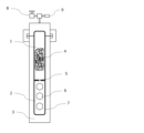
- FIG. 1 is a schematic diagram of a crystal manufacturing apparatus that can be used in one embodiment of the present invention
- FIG. FIG. 4 is a schematic diagram showing an example of a facet growth region in the present disclosure
- FIG. 4 is a schematic diagram showing an example of a method for calculating the facet growth region density in the present disclosure
- the (0001) crystal plane and the (000-1) crystal plane are collectively called the c-plane, the ⁇ 10-10 ⁇ crystal plane is called the m-plane, and the ⁇ 11-20 ⁇ crystal plane is called the a-plane.
- a crystal axis perpendicular to the c-plane is called a c-axis, a crystal axis perpendicular to the m-plane is called an m-axis, and a crystal axis perpendicular to the a-plane is called an a-axis.
- the [0001] direction may be expressed as +c direction
- the [000-1] direction may be expressed as -c direction.
- Gallium nitride according to one embodiment of the present invention, a method for producing the same, and a crystal production apparatus and members used for the production will be described below in detail. The description of the constituent elements described below may be made based on representative embodiments of the present invention, but the present invention is not limited to such embodiments.
- the numerical range represented by "-" means a range including the numerical values before and after "-" as lower and upper limits.
- a first embodiment of the present invention relates to gallium nitride crystals.
- a first aspect of the gallium nitride (GaN) crystal (hereinafter also simply referred to as “GaN crystal”) according to the first embodiment of the present invention is that the inclination from the (000-1) crystal plane is 0 degrees or more and 10 It is a gallium nitride crystal having a main surface 1 of which the degree is less than or equal to the degree, and the main surface 1 is a specific main surface A that satisfies the following condition (A1).
- a first line segment which is a virtual line segment with a length of 40 mm extending in the first direction on the specific main surface A, and a second direction perpendicular to the first direction on the specific main surface A
- a second line segment which is a virtual line segment with a length of 40 mm, can be drawn, and the facet growth region density in any 1 cm ⁇ 1 cm square region on the specific main surface A does not exceed 100 cm ⁇ 2 .
- the GaN crystal of the first aspect preferably has main surface 2 inclined from the (0001) crystal plane, which is the main surface on the opposite side of main surface 1, by 0 degrees or more and 10 degrees or less.
- a second aspect of the GaN crystal according to one embodiment of the present invention has a main surface 1 inclined from the (000-1) crystal plane by 0 degrees or more and 10 degrees or less, and the main surface 1 has the following It is a gallium nitride crystal, which is a specific main surface A that satisfies the condition (A2).
- a first line segment which is a virtual line segment with a length of 40 mm extending in the first direction on the specific main surface A, and a second direction perpendicular to the first direction on the specific main surface A
- a second line segment which is a virtual line segment with a length of 40 mm, can be drawn, and at least one square region of 2 cm ⁇ 2 cm with a facet growth region density of less than 5 cm ⁇ 2 is found in the specific main surface A.
- the GaN crystal of the second embodiment preferably has main surface 2 inclined from the (0001) crystal plane, which is the main surface on the opposite side of main surface 1, by 0 degrees or more and 10 degrees or less.
- a third aspect of the GaN crystal according to one embodiment of the present invention is the principal surface 1 whose inclination from the (000-1) crystal plane is 0 degrees or more and 10 degrees or less, and the opposite principal surface (0001 )
- a gallium nitride crystal having a main surface 2 inclined from the crystal plane by 0 degrees or more and 10 degrees or less, and the main surface 1 being a specific main surface A that satisfies the following condition (A3).
- a first line segment which is a virtual line segment with a length of 40 mm extending in the first direction on the specific main surface A, and a second direction perpendicular to the first direction on the specific main surface A
- a second line segment that is a virtual line segment with a length of 40 mm can be drawn, and the ratio of the area of the facet growth region to the area of the specific main surface A (area of the facet growth region/area of the specific main surface A) is 10% or less.
- the GaN crystal of the third embodiment preferably has main surface 2 inclined from the (0001) crystal plane, which is the main surface on the opposite side of main surface 1, by 0 degrees or more and 10 degrees or less.
- the facet growth region refers to a closed region crystal-grown in a plane orientation different from that of the main surface 1 .
- the plane orientation is not particularly limited, examples thereof include the (10-1-1) plane and the (10-1-2) plane.
- the shape of the faceted growth region is not particularly limited, but typically can be hexagonal or polygonal.
- the facet growth region can typically occur as a pit structure, but the facet growth region in the present disclosure is not limited to the pit structure.
- the concept includes the case where a facet growth region exists on the surface when the pit structure is removed by polishing the main surface. Examples of aspects of faceted growth regions are described.
- the facet growth region is typically observed as a hexagon or polygon on the main surface 1, but when viewed from a cross section perpendicular to the main surface 1, it is observed as a hexagonal or polypyramidal shape. Sometimes.
- the hexagonal or polygonal diameter is typically 5-300 ⁇ m.
- FIG. 2(a) shows an example of such a case.
- the facet growth region may be observed as a shape in which these are integrated on the main surface 1 .
- a plurality of vertexes of hexagonal pyramids or polygonal pyramids can be observed separately.
- the facets described later are used.
- the number of facet growth regions may be counted based on the number of vertices.
- FIG. 2(b) shows an example of such a case.
- the facet growth region density refers to the number of facet growth regions observed in an arbitrary square region on the main surface 1 divided by the area of the square region. Specifically, in (A1) above, the number of facet growth regions observed in a square region of 1 cm ⁇ 1 cm is divided by the area of the square region. In (A2) above, the number of facet growth regions observed in a square region of 2 cm ⁇ 2 cm is divided by the area of the square region.
- the method for observing the number of facet growth regions is not particularly limited as long as the facet growth region can be identified. A method of observing a yellow band bright region in a photoluminescence (PL) image can be used.
- the GaN crystal in the first aspect has a specific primary surface A that satisfies the condition (A1). That is, when an arbitrary square area of 1 cm ⁇ 1 cm is taken on the main surface 1 of the GaN crystal, the facet growth area density in the square area must not exceed 500 cm ⁇ 2 for all square areas.
- the facet growth region density is preferably 100 cm ⁇ 2 or less, more preferably 80 cm ⁇ 2 or less, still more preferably 50 cm ⁇ 2 or less, even more preferably 30 cm ⁇ 2 or less, and particularly preferably 10 cm ⁇ 2 or less. In this case, a GaN substrate having few defects and excellent yield in forming devices can be obtained with good productivity.
- the GaN crystal in the second aspect has a specific primary surface A that satisfies the condition (A2). That is, it is necessary to find at least one square region of 2 cm ⁇ 2 cm with a facet growth region density of less than 5 cm ⁇ 2 on the main surface 1 of the GaN crystal.
- the facet growth region density is preferably less than 4 cm ⁇ 2 , more preferably 3 cm ⁇ 2 or less, and most preferably less than 2 cm ⁇ 2 . In this case, a GaN substrate having few defects and excellent yield in forming devices can be obtained with good productivity.
- the GaN crystal in the third aspect has a specific main surface A that satisfies the condition (A3). That is, the area ratio of the sum of the facet growth regions to the area of the specific main surface A of the GaN crystal (sum of the facet growth regions/the area of the specific main surface A) should be 40% or less.
- the area ratio of the sum of facet growth regions to the area of the specific main surface A is preferably 20% or less, more preferably 10% or less, even more preferably 8% or less, and 6% or less. It is even more preferable that the content be 5% or less, and particularly preferably 5% or less.
- the specific main surface A further satisfies either the condition (A2) or (A3). That is, the GaN crystal preferably has a specific main surface A in which the main surface 1 simultaneously satisfies the condition (A1) and the condition (A2) or the condition (A3). In the GaN crystal in the first aspect, it is particularly preferable that the main surface 1 has a specific main surface A that simultaneously satisfies the conditions (A1), (A2) and (A3).
- the specific main surface A further satisfies the condition (A3). That is, the GaN crystal preferably has a specific main surface A in which the main surface 1 satisfies the conditions (A2) and (A3) at the same time.
- the shape of the GaN crystal is not particularly limited, and may be an amorphous bulk shape or a plate shape. It may be a hexagon or a polygon such as an octagon. Also, the GaN crystal is preferably a GaN single crystal. The structure and characteristics of a plate-like GaN crystal with a circular surface shape will be described below as an example, but the description can be applied to shapes other than this within the applicable range.
- the thickness of the GaN crystal is not particularly limited, but may be 100 ⁇ m or more, 150 ⁇ m or more, 250 ⁇ m or more, 300 ⁇ m or more, 400 ⁇ m or more, 500 ⁇ m or more, 750 ⁇ m or more, 1 mm or more, 2 mm or more, or less than 5 mm or less than 2 mm. , less than 1 mm, less than 750 ⁇ m, less than 500 ⁇ m, less than 400 ⁇ m, less than 300 ⁇ m, less than 250 ⁇ m, and the like. Although there is no particular upper limit to the thickness, it is usually 20 mm or less. If the GaN crystal is in an amorphous bulk, the crystal growth direction preferably satisfies these numerical ranges.
- the diameter of the main surface of the GaN crystal is not particularly limited, but is preferably 45 mm or more, and may be stepwise 50 mm or more, 60 mm or more, 80 mm or more, and 100 mm or more. Typically 45-55 mm (about 2 inches), 95-105 mm (about 4 inches), 145-155 mm (about 6 inches), 195-205 mm (about 8 inches), 295-305 mm (about 12 inches), etc. is.
- the maximum possible length of the surface preferably satisfies these numerical ranges, and the maximum possible length of the surface satisfies these numerical ranges. It is preferred that the minimum length possible on the surface satisfies these numerical ranges.
- the GaN crystal when the GaN crystal is in an amorphous bulk shape, it is preferable that the maximum possible length of the cross section perpendicular to the growth direction of the crystal satisfies these numerical ranges.
- the surface area of the main surface of the GaN crystal is not particularly limited, but is preferably 15 cm 2 or more and less than 50 cm 2 , 50 cm 2 or more and less than 100 cm 2 , 100 cm 2 or more and less than 200 cm 2 , 200 cm 2 or more and less than 350 cm 2 , 350 cm 2 or more and less than 500 cm 2 , 500 cm 2 or more and less than 750 cm 2 , and the like.
- the GaN crystal is in an amorphous bulk, it is preferable that the maximum possible area of the cross section perpendicular to the growth direction of the crystal satisfies these numerical ranges.
- the crystal form of the main surface of the GaN crystal is not particularly limited, and may be, for example, the c-plane, the a-plane, or the m-plane, but the c-plane is particularly preferred.
- the concentration of elements contained as impurities in a GaN crystal is generally measured by SIMS (Secondary Ion Mass Spectrometry).
- the concentration of hydrogen (H) in the GaN crystal is preferably 2 ⁇ 10 19 atoms/cm 3 or less, more preferably 1 ⁇ 10 19 atoms/cm 3 or less, still more preferably 5 ⁇ 10 18 atoms/cm 3 or less, Particularly preferably, it is 1 ⁇ 10 18 atoms/cm 3 or less.
- the GaN crystal of this embodiment is grown by the ammonothermal method, it can contain H (hydrogen) at a concentration of 1 ⁇ 10 17 atoms/cm 3 or higher.
- the concentration of oxygen (O) in the GaN crystal is preferably 2 ⁇ 10 19 atoms/cm 3 or less, more preferably 1 ⁇ 10 19 atoms/cm 3 or less, and even more preferably 5 ⁇ 10 18 atoms/cm 3 . Below, it is particularly preferably 1 ⁇ 10 18 atoms/cm 3 or less. Further, since the GaN crystal of the present embodiment is grown by the ammonothermal method, H (hydrogen) is 1 ⁇ 10 17 atoms/cm 3 or more and O (oxygen) is 1 ⁇ 10 17 atoms/cm 3 or more. concentration.
- the GaN crystal of this embodiment may contain a halogen element in the crystal.
- Halogen elements can be introduced, for example, by mineralizers used in ammonothermal processes.
- a good example of the halogen element that may be included is fluorine (F).
- F When a GaN crystal is grown by an ammonothermal method using a mineralizer containing F, F may be contained at a concentration of 1 ⁇ 10 15 atoms/cm 3 or more, preferably 1 ⁇ 10 18 . It is atoms/cm 3 or less, more preferably 5 ⁇ 10 17 atoms/cm 3 or less, and still more preferably 1 ⁇ 10 17 atoms/cm 3 or less.
- Halogen elements other than fluorine that the GaN crystal may contain include chlorine (Cl), bromine (Br), iodine (I), and the like, but fluorine is the only halogen element substantially contained in the GaN crystal. is preferably Such crystals are obtained, for example, by using only mineralizers containing F as the halogen.
- the crystal contains a halogen element, substantially contains only fluorine, and has a main surface 1 inclined from the (000-1) crystal plane by 0 degrees or more and 10 degrees or less, wherein the main surface A gallium nitride crystal, wherein 1 is a specific main surface A that satisfies at least one of the following conditions (A1) to (A3).
- a first line segment which is a virtual line segment with a length of 40 mm extending in the first direction on the specific main surface A, and a second direction perpendicular to the first direction on the specific main surface A
- a second line segment that is a virtual line segment with a length of 40 mm can be drawn, and the facet growth region density in an arbitrary 10 mm ⁇ 10 mm square region on the specific main surface A does not exceed 500 cm -2 , preferably does not exceed 100 cm -2
- A2 a first line segment that is a virtual line segment with a length of 40 mm extending in the first direction on the specific main surface A, and a first line segment on the specific main surface A in the first direction A 20 mm ⁇ 20 mm square area with a facet growth area density of less than 5 cm ⁇ 2 can be drawn, and a second line segment that is a virtual line segment with a length of 40 mm extending in a second direction perpendicular to the specific main surface At least one found in A (A3) a first
- the fact that the halogen element substantially contained in the GaN crystal is only fluorine means that the total content of halogen elements other than F in the crystal is 1/100 or less of the content of F. say.
- members used in the reaction vessel for example, lining material
- the total content of halogen elements other than F in the crystal is more preferably 1/150 or less, more preferably 1/200 or less of the content of F.
- the main crystal contains F in the crystal, the total content of halogen elements other than F is 1/100 or less of the content of F, and the inclination from the (000-1) crystal plane is 0 degrees or more and 10 degrees or less
- a first line segment which is a virtual line segment with a length of 40 mm extending in the first direction on the specific main surface A, and a second direction perpendicular to the first direction on the specific main surface A
- a second line segment that is a virtual line segment with a length of 40 mm can be drawn, and the facet growth region density in an arbitrary 10 mm ⁇ 10 mm square region on the specific main surface A does not exceed 500 cm -2 , preferably does not exceed 100 cm -2
- A2 a first line segment that is a virtual line segment with a length of 40 mm extending in the first direction on the specific main surface A, and a first line segment on the specific main surface A in the first direction A 20 mm ⁇ 20 mm square area with a facet growth area density of less than 5 cm ⁇ 2 can be drawn, and a second line segment that is a virtual line segment with a length of 40 mm extending in a second direction perpendicular to the specific main surface At least one found in A (A3) a first
- the concentrations of lithium (Li), sodium (Na) and potassium (K) are each 1 ⁇ 10 15 atoms. /cm 3 .
- the Fe concentration can be achieved in the order of 10 15 atoms/cm 3 or less, and the Ni concentration can be achieved in the order of 10 15 atoms/cm 3 or less.
- the dislocation density which is an index of the density of linear defects in the GaN crystal, is not particularly limited, but is preferably 1 ⁇ 10 6 cm ⁇ 2 or less, more preferably 5 ⁇ 10 5 cm ⁇ 2 or less, and more preferably 5 ⁇ 10 5 cm ⁇ 2 or less. It is preferably 1 ⁇ 10 5 cm ⁇ 2 or less, and usually 1 ⁇ 10 2 cm ⁇ 2 or more.
- the dislocation density of the GaN crystal is usually 10 6 cm ⁇ 2 or more.
- the GaN crystal preferably does not have a facet growth region with a diameter of 2 mm or more in the specific main surface A, and more preferably does not have a facet growth region with a diameter of 1.5 mm or more.
- the GaN crystal has a first line segment which is a virtual line segment with a length of 40 mm extending in the first direction on the specific main surface A, and a second direction perpendicular to the first direction on the specific main surface A. It is necessary to be able to draw a second line segment, which is a virtual line segment with a length of 40 mm extending to .
- the specific main surface A preferably further satisfies at least one of the following conditions (B1) and (B2).
- XRC is an X-ray rocking curve (or X-ray diffraction rocking curve), and its FWHM (Full Width at Half Maximum) is an index generally used for crystal quality evaluation.
- the difference between the maximum value and the minimum value of the XRC peak angle referred to in the above condition (B2) simply represents how much the c-axis direction of the GaN single crystal fluctuates on the first line segment.
- At least one of the first line segments that can be drawn on the main surface of the GaN single crystal according to the first embodiment preferably passes through the center (center of gravity) of the main surface, but is not limited. .
- the maximum FWHM is preferably less than 30 arcsec, more preferably less than 20 arcsec.
- the difference between the maximum and minimum values of the XRC peak angles between all measurement points is preferably less than 0.1°, more preferably less than 0.05°.
- the GaN crystal preferably has a radius of curvature in the a-axis direction of 5 m or more, more preferably 10 m or more, even more preferably 20 m or more, and particularly preferably 30 m or more.
- a GaN crystal grown by the ammonothermal method can have a peak at 3140-3200 cm ⁇ 1 in the infrared absorption spectrum.
- a second embodiment of the present invention relates to a gallium nitride (GaN) crystal.
- GaN gallium nitride
- One aspect of the GaN crystal according to the second embodiment of the present invention is the principal surface 1 inclined from the (000-1) crystal plane by 0 degrees or more and 10 degrees or less, and the opposite principal surface (0001 ) has a main surface 2 with an inclination of 0 degrees or more and 10 degrees or less from the crystal plane, a thickness in the c-axis direction of 1 mm or more, and an area ratio between the main area 1 and the main area 2 (main area 1/main area 2 ) is 0.5 or more and 1 or less.
- the area ratio of the main area 1 and the main area 2 (main area 1/main area 2) is preferably 0.6 or more, more preferably 0.7 or more, and still more preferably 0.8 or more. The closer the area ratio between the main area 1 and the main area 2 is to 1, the easier it is to obtain a GaN substrate having a larger area from the GaN crystal, and the productivity of the GaN substrate is improved.
- One aspect of the GaN crystal according to the second embodiment of the present invention is the principal surface 1 inclined from the (000-1) crystal plane by 0 degrees or more and 10 degrees or less, and the opposite principal surface (0001 ) has a main surface 2 inclined from the crystal plane by 0 degrees or more and 10 degrees or less, a thickness in the c-axis direction of 1 mm or more, and the (10-1-1) plane and the (10-1-2) plane It is a gallium nitride crystal whose area ratio satisfies the following relational expression (C). (10-1-2) plane area/ ⁇ (10-1-1) plane area + (10-1-2) plane area ⁇ ⁇ 0.5 (C)
- the area ratio between the (10-1-1) plane and the (10-1-2) plane is preferably less than 0.4, more preferably less than 0.3, and 0.4. Less than 3 is more preferred.
- the same GaN crystal according to the first embodiment can be applied.
- a third embodiment of the present invention relates to a method for manufacturing a GaN crystal.
- the GaN single crystal production method according to the third embodiment can be used, for example, to produce the GaN crystals according to the first and second embodiments described above.
- the method for producing a GaN crystal according to the present embodiment includes a seed preparation step of preparing a GaN seed having a nitrogen-polar surface obtained by liquid phase epitaxy; and a crystal growth step of growing a GaN crystal on the nitrogen-polar surface of the GaN seed by an ammonothermal method at a growth temperature of 600° C. or higher.
- This step is a step of preparing a GaN seed having a nitrogen polar surface obtained by liquid phase epitaxy.
- a typical example of a GaN seed is a C-plane GaN substrate.
- the main surface on the [0001] side is a gallium polar surface
- the main surface on the [000-1] side is a nitrogen polar surface.
- the GaN seed prepared in this step is obtained by liquid phase epitaxy.
- a known technique can be employed as the liquid phase growth method, and examples thereof include the ammonothermal method and the Na flux method. Among them, GaN seeds obtained by the ammonothermal method are preferable, and GaN seeds obtained by the acidic ammonothermal method are particularly preferable.
- a GaN crystal in which the occurrence of specific crystal defects is suppressed can be obtained by using a GaN seed obtained by liquid phase epitaxy as a seed crystal and by satisfying the crystal growth conditions described later. rice field.
- the facet growth region is considered to be generated when defects or the like on the surface of the GaN seed used for growth serve as starting points for facet growth.
- a GaN seed obtained by a liquid phase epitaxy has a lower dislocation density than a GaN seed obtained by, for example, a vapor phase epitaxy, and has fewer defects such as stress concentration portions caused by dislocations. It is thought that there are few defects that can be starting points, and the occurrence of facet growth regions is suppressed.
- the surface (growth surface) of the GaN seed for crystal growth on the GaN seed should have few defects that can serve as starting points for facet growth.
- the dislocation density of the growth surface of the GaN seed is preferably less than 1 ⁇ 10 7 cm ⁇ 2 , more preferably 5 ⁇ 10 6 cm ⁇ 2 or less, and more preferably 1 ⁇ 10 6 cm ⁇ 2 . Below is more preferred, and below 5 ⁇ 10 5 cm ⁇ 2 is even more preferred. A lower dislocation density is more desirable, but the lower limit is usually 1 ⁇ 10 2 cm ⁇ 2 or more. It is desirable that the surface (growth surface) of the GaN seed for crystal growth on the GaN seed should have few defects that can serve as starting points for facet growth.
- the growth surface of the GaN seed does not have a dislocation concentrated region where dislocations are relatively concentrated.
- Dislocation concentrated regions may be formed intentionally. For example, when aiming to reduce dislocations by intentionally concentrating dislocations by forming a specific mask pattern in order to reduce dislocations on the entire crystal surface, a dislocation-concentrated region where dislocations are locally concentrated is formed on the crystal surface. may remain. The presence of dislocation-concentrated regions can generate local stress and serve as starting points for facet growth.
- a specific example of the surface (growth surface) of the GaN seed for crystal growth on the GaN seed is the nitrogen-polar surface of the GaN seed.
- the orientation of the nitrogen-polar surface of the GaN seed is preferably within 2° from [000-1], expressed in the direction of the normal vector. This means that the angle between the normal vector of the nitrogen polar surface and [000-1] is within 2°.
- the orientation of the nitrogen polar surface of the GaN seed is more preferably within 1° from [000-1].
- the area of the nitrogen-polar surface of the GaN seed is 15 cm 2 or more and less than 50 cm 2 , 50 cm 2 or more and less than 100 cm 2 , 100 cm 2 or more and less than 200 cm 2 , 200 cm 2 or more and less than 350 cm 2 , 350 cm 2 or more and less than 500 cm 2 , 500 cm 2 or more and 750 cm 2 . can be less than, and so on.
- the diameter is usually greater than or equal to 45 mm and less than or equal to 305 mm.
- the diameter is preferably 45 mm or more, and can be stepwise 50 mm or more, 60 mm or more, 80 mm or more, and 100 mm or more.
- 45-55 mm about 2 inches
- 95-105 mm about 4 inches
- 145-155 mm about 6 inches
- 195-205 mm about 8 inches
- 295-305 mm about 12 inches
- the GaN seed is a C-plane GaN substrate with a diameter of 50 mm
- its thickness is preferably 300 ⁇ m or more, and the larger the diameter, the larger the preferable lower limit of its thickness.
- the thickness of the GaN seed it is usually 20 mm or less.
- the size of the GaN seed is determined in consideration of the size of the GaN crystal to be grown in the subsequent crystal growth process. For example, when cutting out a C-plane GaN substrate having a size of 45 mm in the [1-100] direction, the [10-10] direction, and the [01-10] direction from a GaN crystal to be grown, the GaN crystal should be grown so that the sizes in the [1-100] direction, [10-10] direction and [01-10] direction are all 45 mm or more.
- the [1-100] direction, the [10-10] 10] direction and [01-10] direction size is preferably 45 mm or more.
- the nitrogen-polar surface of the GaN seed is typically planarized by polishing or grinding.
- the damaged layer introduced by the planarization process is removed from the nitrogen polar surface by CMP (Chemical Mechanical Polishing) and/or etching.
- the dislocation density of the GaN seed is not particularly limited, it is preferably 1 ⁇ 10 6 cm ⁇ 2 or less, more preferably 5 ⁇ 10 5 cm ⁇ 2 or less, and still more preferably 1 ⁇ 10 5 cm ⁇ 2 or less. and is usually 1 ⁇ 10 2 cm ⁇ 2 or more.
- This step is a step of growing a GaN crystal on the nitrogen-polar surface of the GaN seed by the ammonothermal method.
- a GaN crystal is grown on the nitrogen-polar surface of the GaN seed by the ammonothermal method at a growth temperature of 600° C. or higher.
- the nitrogen-containing solvent is placed in a supercritical state and/or Alternatively, it includes a step of growing a GaN crystal on the surface of the GaN seed by controlling it to be in a subcritical state.
- the present inventors have found that a GaN crystal in which the occurrence of specific crystal defects is suppressed can be obtained by using the GaN seed described above and satisfying the crystal growth conditions described above. Although the detailed reason for this is not yet clear, it is speculated as follows. Formation of the facet growth region on the nitrogen polar surface of the GaN crystal is such that the crystal growth speed in the direction of the facet plane is relatively slow compared to the crystal growth speed in the direction of the (000-1) plane, so that the facet growth region is buried. It is thought that it depends on continuing to exist without being cut off. Specifically, it is considered that the growth rate of the facet plane represented by the (10-1-1) plane and the (10-1-2) plane is lower than that of the (000-1) plane.
- the growth rate in the specific facet plane direction can be improved by setting the pressure in the reaction vessel to 200 MPa or lower and the temperature of the crystal growth region to 600° C. or higher, which is higher than conventionally. rice field. It is believed that this reduces the relative difference in crystal growth rate between the (000-1) plane direction and the facet plane direction, thereby suppressing the formation of facet growth regions. It is speculated that the facet growth region density can be dramatically improved by a synergistic effect in combination with the suppressive effect of employing the GaN seed obtained by the liquid phase epitaxy described above. In addition, as will be described later, it is also possible to effectively reduce the facet growth region density by reducing the amount of foreign matter externally adhering to the growth surface of the GaN seed.
- the present inventors have found that a GaN crystal having a large area ratio (main surface 1/main surface 2) between main surface 1 and main surface 2 can be obtained by using the above-described GaN seed and satisfying the above-described crystal growth conditions. I found what I got. Although the detailed reason for this is not yet clear, it is speculated as follows. According to the conventional method, among the facet planes formed around the main surface, the growth rate of the facet plane having a gentler inclination with respect to the c-axis direction (for example, the (10-1-2) plane) has a steeper inclination.
- the growth rate is lower than that of a flat facet plane (for example, the (10-1-1) plane), the area of the gently slanted facet plane expands, and along with this, the main surface on the side of the nitrogen polar surface (main surface 1 ) is thought to have shrunk.
- the crystal growth rate in the direction of the specific facet plane can be improved, so that the expansion of the area of the specific facet plane is suppressed, and the reduction of the area of the main surface 1 is suppressed. It is possible.
- a GaN crystal having a larger area ratio (main surface 1/main surface 2) between main surface 1 and main surface 2 than the conventional one can be obtained.
- the mineralizer is not particularly limited as long as it contains fluorine.
- fluorine-containing mineralizers include ammonium fluoride, hydrogen fluoride, and hydrocarbylammonium fluoride, tetramethylammonium fluoride, tetraethylammonium fluoride, benzyltrimethylammonium fluoride, dipropylammonium fluoride, and alkylammonium salts such as isopropylammonium fluoride, alkylmetal fluorides such as sodium alkylfluoride, alkaline earth metal fluorides, and metal fluorides.
- alkali fluorides, alkaline earth metal fluorides, metal fluorides, ammonium fluoride, and hydrogen fluoride are preferred, and alkali fluorides, ammonium fluoride, and group 13 metal fluorides of the periodic table are more preferred.
- Ammonium fluoride (NH 4 F) and gallium fluoride are particularly preferred. High-quality crystals with good crystallinity tend to be obtained by using mineralizers containing fluorine. More preferably, a mineralizer containing only fluorine as a halogen element is used.
- fluorine-containing mineralizer only a fluorine-containing mineralizer may be used, or a mixture of a fluorine-containing mineralizer and a fluorine-free mineralizer may be used.
- fluorine-free mineralizers include acidic mineralizers composed of halogens other than fluorine and ammonium ions, such as ammonium chloride, ammonium iodide, and ammonium bromide; lithium chloride, lithium bromide, lithium iodide, chloride Neutral mineralizers consisting of alkali metals and halogens such as sodium, sodium bromide, sodium iodide, potassium chloride, potassium bromide, potassium iodide; beryllium chloride, beryllium bromide, beryllium iodide, magnesium chloride, bromide Neutral mineralizers consisting of alkaline earth metals and halogens such as magnesium, magnesium iodide, calcium chloride, calcium bromide, calcium iodide;
- the ratio of the fluorine-containing mineralizer to the total mineralizer is preferably 50 mol% or more, and 60 mol% or more. is more preferable, and 80 mol % or more is even more preferable.
- mineralizers that do not contain fluorine mineralizers that contain halogen other than fluorine are used from the viewpoint of controlling the shape of grown crystals using the orientation dependence of the growth rate of mineralizers and controlling the precipitation of miscellaneous crystals.
- fluorine accounts for preferably 50% or more, more preferably 60% or more, and even more preferably 80% or more of the total halogen in the mineralizer. .
- the mineralizer preferably exhibits negative solubility characteristics in a nitrogen-containing solvent near the temperature at which the GaN crystal is grown.
- ammonium fluoride exhibits a negative solubility characteristic with respect to ammonia in a temperature range of 400° C. or higher. Since it is usually preferable to set the temperature of the crystal growth region to 450° C. or higher, when only ammonium fluoride is used as the mineralizer, ammonium fluoride exhibits negative solubility characteristics at the crystal growth temperature.
- the slope of the solubility curve determined based on each solubility characteristic changes according to the mixing ratio. If the absolute value of the slope of the solubility curve is small, the efficiency of crystal growth will be poor, so the mixing ratio is adjusted so that the solubility curve with an appropriate slope is shown.
- the molar concentration of fluorine contained in the mineralizer with respect to the nitrogen-containing solvent is preferably 0.2 mol% or more, more preferably 0.27 mol% or more, still more preferably 1.0 mol% or more, and particularly preferably 1.5 mol% or more. Also, it is preferably 30 mol % or less, more preferably 20 mol % or less, still more preferably 10 mol % or less, and particularly preferably 2 mol % or less.
- concentration is high, the solubility of the raw material in the nitrogen-containing solvent is improved, and the growth rate tends to increase, which is preferable.
- the concentration is low, the solubility can be maintained at an appropriate level, so spontaneous nucleation can be suppressed, and the degree of supersaturation can be kept low, which facilitates control, which is preferable.
- the pressure inside the reactor during crystal growth is set to 200 MPa or less to grow the crystal.
- the pressure in the reaction vessel is preferably 5 MPa or higher, more preferably 10 MPa or higher, even more preferably 12 MPa or higher, particularly preferably 15 MPa or higher, most preferably 20 MPa or higher. It is preferably 150 MPa or less, more preferably 120 MPa or less, and even more preferably 100 MPa or less.
- the manufacturing method of this embodiment is characterized in that a GaN crystal can be efficiently grown even under a relatively low pressure. If the crystal is grown at a relatively low pressure, the wall thickness of the pressure-resistant container can be reduced, and the energy efficiency can be improved to reduce the cost.
- GaN seed As the GaN seed used in the crystal growth step, one prepared in the GaN seed preparation step described above can be used.
- Nitrogen-containing solvents include solvents that do not impair the stability of the grown GaN crystal.
- the solvent include ammonia, hydrazine, urea, amines (e.g., primary amines such as methylamine, secondary amines such as dimethylamine, tertiary amines such as trimethylamine, and ethylenediamine). diamine), melamine, and the like. These solvents may be used alone or in combination.
- the amount of water and oxygen contained in the solvent is desirably as small as possible, and the content thereof is preferably 1000 ppm or less, more preferably 10 ppm or less, and even more preferably 0.1 ppm or less.
- ammonia is used as a solvent, its purity is usually 99.9% or higher, preferably 99.99% or higher, more preferably 99.999% or higher.
- the raw material a raw material containing elements constituting the GaN crystal to be grown on the seed crystal is used.
- Polycrystalline raw materials for GaN crystals and/or metals to be nitrided are preferred, and gallium nitride and/or metallic gallium are more preferred.
- the polycrystalline raw material does not need to be a complete nitride, and depending on the conditions, it may contain a metal component in which an element of Group 13 of the periodic table is in a metal state (zero valence).
- the crystal is gallium nitride. In some cases, a mixture of gallium nitride and gallium metal is included.
- the method for producing the polycrystalline raw material is not particularly limited.
- a nitride polycrystal produced by reacting a metal or its oxide or hydroxide with ammonia in a reaction vessel in which ammonia gas is passed can be used.
- compounds having a covalent MN bond such as halides, amide compounds, imide compounds, and galazanes can be used as metal compound raw materials with higher reactivity.
- a nitride polycrystal produced by reacting a metal such as Ga with nitrogen at high temperature and high pressure can also be used.
- the amount of water and oxygen contained in the polycrystalline raw material used as the raw material is small.
- the oxygen content in the polycrystalline raw material is usually 10000 ppm or less, preferably 1000 ppm or less, and particularly preferably 1 ppm or less.
- the susceptibility of polycrystalline raw material to oxygen contamination is related to its reactivity with or absorption of moisture. The worse the crystallinity of the polycrystalline raw material is, the more active groups such as NH groups are present on the surface, which may react with water to partially form oxides and hydroxides. For this reason, it is generally preferable to use a polycrystalline raw material having as high a crystallinity as possible.
- reaction vessel A GaN crystal growth reaction is performed in a reaction vessel.
- the reaction vessel means a vessel for producing a GaN crystal in a state in which a nitrogen-containing solvent in a supercritical state and/or a subcritical state can come into direct contact with the inner wall surface of the vessel.
- a capsule placed in a pressure-resistant container, and the like can be mentioned as preferable examples.
- the pressure-resistant part of the reaction vessel is preferably composed of any one of Ni-based alloy, Fe-based alloy, cobalt-based alloy, or a combination of these alloys, and is particularly preferably made of Ni--Fe-based alloy (Ni--Fe It is particularly preferable that the base alloy has an Fe content of 30 to 40% by mass and that Cr, Ti, Al, and Nb are contained as other elements).
- the manner in which the reaction vessel is constructed from these alloys is not particularly limited.
- the reaction vessel may be formed by directly lining or coating the inner surface of the pressure-resistant part with a material having excellent corrosion resistance, or a capsule made of a material having excellent corrosion resistance may be arranged in the pressure-resistant vessel.
- the shape of the reaction vessel can be any shape including cylindrical shape.
- the reaction vessel may be used in an upright position, in a horizontal position, or in an oblique position, but it is particularly preferable to use it in an upright position.
- Platinum group or platinum group alloy can be used for the lining material and capsule as the corrosion resistant part.
- the platinum group includes Pt, Au, Ir, Ru, Rh, Pd, Ag.
- Ag or an alloy containing Ag can be suitably used as the lining material by using a fluorine-containing compound alone as the mineralizer.
- GaN seeds are prepared by controlling the solvent in a supercritical and/or subcritical state in a reaction vessel containing the GaN seed, nitrogen-containing solvent, raw material, and mineralizer prepared in the seed preparation step. ) to grow a GaN crystal on the surface.
- the pressure conditions at this time are as described above.
- the temperature during growth is set to different temperatures in the raw material dissolving region where the raw material is melted and the crystal growth region where the crystal is grown on the seed crystal.
- the temperature of the crystal growth region should be 600° C. or higher. It is more preferably 610° C. or higher. Also, the temperature of the crystal growth region may be higher, but can be preferably set to, for example, 700° C.
- the temperature of the raw material dissolution zone is set higher than the temperature of the crystal growth zone when using mineralizers with negative solubility characteristics. Also, when using a mineralizer with a positive solubility characteristic, the temperature is set lower than the temperature of the crystal growth region.
- the temperature difference between the raw material melting region and the crystal growth region is usually set to 30° C. or higher, preferably 40° C. or higher, and usually set to 150° C. or lower, preferably 120° C. or lower. It is also preferable to etch the surface of the GaN seed by adjusting the solubility at the initial stage of crystal growth. As a result, the surface layer portion of the GaN seed is dissolved, and the damaged layer that can serve as a starting point for facet growth can be removed.
- the crystal By growing the GaN crystal under the conditions described above, the crystal can be grown at a relatively high growth rate.
- the crystal growth rate can be 300 ⁇ m/day or more, 500 ⁇ m/day or more, 700 ⁇ m/day or more, and furthermore It is also possible to make it 900 ⁇ m/day or more.
- Preparation process In addition to the above growth step, there may be a preparatory step prior to the above growth step, in which the GaN seed, the nitrogen-containing solvent, and the raw material are placed in the reaction vessel.
- the method of putting these materials into the reaction vessel is not particularly limited, and examples include a method of placing seed crystals in the lower part of the reaction vessel and starting materials in the upper part of the reaction vessel, and then pouring the nitrogen-containing solvent.
- the surface (growth surface) of the GaN seed for crystal growth on the GaN seed should desirably have few growth-inhibiting factors that can serve as starting points for facet growth.
- crystal defects such as dislocations that are inherent in the GaN seed can be cited as factors that inhibit growth that can serve as starting points for facet growth. It can be a factor inhibiting growth.
- foreign matter include impurities existing on the inner wall of the reaction vessel, fine particles of GaN polycrystals used as raw materials, and the like.
- the direction of the growth surface of the GaN seed when the GaN seed is placed in the reaction vessel should be parallel to the height direction of the reaction vessel or downward. It is preferred to have an angle. In this case, foreign matter can be prevented from adhering to the growth surface of the GaN seed externally, which is desirable from the viewpoint of suppressing facet growth.
- the cleaning method is not particularly limited, foreign matter adhering to the inner wall can be removed by, for example, physical cleaning with a brush or the like, or chemical cleaning with acid, alkali, or the like.
- degassing step of heating and degassing the inside of the reaction vessel before the above-described growth step in order to obtain a high-purity GaN crystal.
- oxygen in the reaction vessel can be reduced and the amount of oxygen impurities contained in the GaN crystal can be adjusted.
- the method of degassing by heating is not particularly limited, and can be carried out by a known method, for example, a method of degassing with a vacuum pump while heating.
- the temperature during heating and degassing is not particularly limited, but the temperature range is preferably 80° C. or higher, more preferably 120° C. or higher, still more preferably 160° C.
- the heat degassing time is preferably 2 hours or longer, more preferably 6 hours or longer, still more preferably 12 hours or longer, preferably 72 hours or shorter, more preferably 48 hours or shorter, and particularly preferably 24 hours or shorter.
- a processing process for processing the GaN crystal may be included after the growth process described above.
- the processing for example, slicing the obtained GaN crystal to obtain only the portion having the desired characteristics is conceivable, and it is most preferable to obtain only the portion that satisfies the aforementioned crystal quality requirements.
- the GaN crystal thus obtained can be used as a GaN substrate, which will be described later.
- GaN substrate gallium nitride substrate obtained by slicing the GaN crystal described above, and a manufacturing method thereof.
- the diameter of the GaN substrate is 50 mm or more, typically 50-55 mm (about 2 inches), 100-105 mm (about 4 inches), 150-155 mm (about 6 inches), etc. Since the GaN substrate is required to have a strength that does not interfere with handling, its thickness is usually 250 ⁇ m or more, and may be increased depending on the diameter.
- the thickness is preferably 250 ⁇ m or more, more preferably 300 ⁇ m or more, and preferably 450 ⁇ m or less, more preferably 400 ⁇ m or less.
- the thickness is preferably 350 ⁇ m or more, more preferably 400 ⁇ m or more, and preferably 750 ⁇ m or less, more preferably 650 ⁇ m or less.
- the thickness is preferably 450 ⁇ m or more, more preferably 550 ⁇ m or more, and preferably 800 ⁇ m or less, more preferably 700 ⁇ m or less.
- GaN substrates can preferably be used in the manufacture of nitride semiconductor devices.
- one or more nitride semiconductor layers are epitaxially grown on the main surface of a GaN substrate to form an epitaxial wafer.
- vapor phase methods such as MOVPE (Metal Organic Vapor Phase Epitaxy), MBE (Molecular Beam Epitaxy), PXD (Pulsed Excitation Deposition), sputtering, and HVPE can be preferably used.
- Epitaxially grown nitride semiconductor layers can be made n-conducting, p-conducting or semi-insulating by doping.
- the GaN seed used for the above-described crystal growth is not particularly limited, and any known seed may be used, and it is preferable to use the above-described GaN substrate, which is another embodiment of the present invention.
- the growth conditions of the above-described GaN crystal manufacturing method can be applied to the growth of the GaN crystal on the GaN seed by the ammonothermal method.
- the thickness of the GaN crystal grown on the GaN seed by the ammonothermal method is 500 ⁇ m or more, preferably 600 ⁇ m or more, 700 ⁇ m or more, 800 ⁇ m or more, or 900 ⁇ m or more. good.
- the conditions for the method of manufacturing the GaN substrate the above conditions for the GaN crystal and the GaN substrate can be applied within the applicable range.
- Examples of nitride semiconductor devices that can be manufactured using a GaN substrate include light-emitting devices such as light-emitting diodes (LEDs) and laser diodes (LDs), rectifiers, bipolar transistors, field-effect transistors, HEMTs (High Electron Mobility Transistors), and the like. Examples include electronic devices, temperature sensors, pressure sensors, radiation sensors, semiconductor sensors such as visible-ultraviolet light detectors, and solar cells. Other uses of GaN substrates include growth of bulk GaN crystals by HVPE, THVPE (Tri-Halide Vapor Phase Epitaxy), OVPE (Oxide Vapor Phase Epitaxy), ammonothermal method, Na flux method, and various other methods. seeds, etc.
- HVPE Light-emitting diodes
- LDs laser diodes
- HEMTs High Electron Mobility Transistors
- Examples include electronic devices, temperature sensors, pressure sensors, radiation sensors, semiconductor sensors such as visible-ultraviolet light detectors, and solar cells
- ⁇ Evaluation method> (1) Calculation of facet growth region density Observation was performed with a digital camera while the nitrogen polar plane of the GaN crystal was grown.
- the facet growth region has a concave shape and a diameter of 100 to several hundred ⁇ m, so that it can be easily observed with the naked eye. Observation may also be performed with a microscope, but since it is necessary to observe a wide area of 10 mm ⁇ 10 mm or more, observation at as low a magnification as possible is suitable. As shown in FIG. 3, the facet growth area is counted by taking an arbitrary 10 mm ⁇ 10 mm area on the nitrogen polar plane and further dividing the area into 1 mm ⁇ 1 mm areas.
- the facet growth region density within the 10 mm.times.10 mm area can be obtained.
- an area of 20 mm ⁇ 20 mm is arbitrarily taken on the nitrogen polar surface, and the area is further divided into areas of 1 mm ⁇ 1 mm. The number of facet growth regions in each area was counted and totaled to obtain the number within a 20 mm ⁇ 20 mm area. Furthermore, by dividing by the area of 4 cm 2 , the facet growth region density within an area of 20 mm ⁇ 20 mm was obtained.
- Example 1 a GaN crystal was grown using the reactor shown in FIG. Crystal growth was carried out using an Ni—Fe-based alloy autoclave (ratio of volume to inner surface area: 2.3 (cm)) with an inner surface lined with Ag as a pressure vessel. The operation of filling the container with the outer wall was performed in an air atmosphere. The inner walls of the pressure vessel were cleaned prior to the filling operation. As for the cleaning method, after dissolving deposits on the inner wall using a heated alkaline solution, the inner wall was rubbed and cleaned with a nylon sponge, and then rinsed with pure water.
- Ni—Fe-based alloy autoclave ratio of volume to inner surface area: 2.3 (cm)
- a hexagonal GaN single crystal (68 mm in the m-axis direction ⁇ 60 mm in the a-axis direction ⁇ 0.6 mm in the c-axis direction) grown by the ammonothermal method was used as a seed crystal.
- the (000-1) plane which is the main surface of the seed crystal, was sliced with a wire saw and then etched with KOH.
- This seed crystal 6 was hung from a molybdenum seed crystal support frame with a tungsten wire having a diameter of 0.2 mm, and placed in the crystal growth zone 2 at the bottom of the autoclave.
- the seed crystal was placed so that the (000-1) plane faces slightly downward.
- the dislocation density of the (000-1) plane of the seed crystal was on the order of 10 4 /cm 2 on average. Also, there was no dislocation concentration region.
- a baffle plate 5 made of molybdenum was installed between the lower crystal growth region 2 and the upper raw material melting region 1 . Furthermore, 5800 g of polycrystalline GaN particles were weighed as raw material 4 and placed in the autoclave upper region (raw material melting region 1). Next, sufficiently dried NH 4 F with a purity of 99.9% as a mineralizer source was weighed so as to be 10 mol % with respect to the ammonia to be filled, and put into a pressure vessel.
- the lid of the autoclave fitted with the valve 8 was closed.
- the conduit was then operated to lead to a vacuum pump via valve 8 attached to the autoclave, and the valve 8 was opened for vacuum degassing.
- the autoclave was cooled with a dry ice methanol solvent, and the valve 8 was once closed.
- the valve 8 was opened again, and the autoclave was continuously filled with NH 3 without exposure to the outside air, and then the valve 8 was closed again.
- the temperature of the autoclave was returned to room temperature, the outer surface was sufficiently dried, and the weight of the autoclave was measured.
- the NH 3 filling amount was confirmed by the value of the mass flow meter and adjusted to a filling rate of 33%.
- the autoclave was housed in an electric furnace composed of heaters divided vertically into two.
- the temperature of the raw material melting region 1 on the outer surface of the autoclave was raised to 588.5° C.
- the temperature of the crystal growth region 2 was raised to 617.4° C. (temperature difference of 28.9° C.). It was held at temperature for 14 days.
- the pressure inside the autoclave was 120 MPa.
- the variation in the control temperature of the outer surface of the autoclave during holding was ⁇ 0.5°C or less.
- the surface of the seed crystal was etched by adjusting the solubility to remove the damaged layer.
- the crystal taken out had a thickness in the c-axis direction of 2.7 mm.
- the ratio of the area of the nitrogen polar face of the crystal to the area of the gallium polar face (nitrogen polar face/gallium polar face) was 0.76.
- the ratio of the area of the (10-1-2) plane to the sum of the areas of the (10-1-1) plane and the (10-1-2) plane was 0.22.
- the nitrogen polar plane was visually flat, and the facet growth region was extremely small.
- the XRC of this crystal was measured and the full width at half maximum (FWHM) was 19 arcsec at 002 reflection.
- FWHM full width at half maximum
- ⁇ scan measurement was performed on a line segment of 50 mm in the a-axis direction at intervals of 5 mm, and ⁇ was ⁇ 0.03°. The radius of curvature was calculated to be 50m.
- the number of facet growth regions on the nitrogen polar plane of this crystal was counted.
- An arbitrary 1 cm ⁇ 1 cm measurement area was measured at five locations, and the respective facet growth region densities were 2 cm ⁇ 2 , 94 cm ⁇ 2 , 2 cm ⁇ 2 , 5 cm ⁇ 2 and 0 cm ⁇ 2 .
- 18 were found. Converted to density, it was 4.5 cm ⁇ 2 .
- the ratio of the total area of the facet growth regions to the area of the main area 1 of the present crystal was 4%.
- Example 1 Crystal growth was carried out under exactly the same conditions as in Example 1 except that a GaN crystal grown by the HVPE method was used as a seed crystal (having a nitrogen polar plane as the main surface and a diameter of 50 mm and a dimension in the c-axis direction of 0.6 mm).
- the dislocation density of the seed crystal was on the order of 10 6 /cm 2 on average. Also, dislocation concentrated regions were present.
- the crystal taken out had a thickness of about 3 mm in the c-axis direction.
- the nitrogen polar plane was visually very uneven, and it was impossible to count the number of individual facet growth regions.
- the XRC of this crystal was measured, and the full width at half maximum (FWHM) was 34 to 47 arcsec for 002 reflection.
- FWHM full width at half maximum
- ⁇ scan measurement was performed on a line segment of 40 mm in the a-axis direction at intervals of 5 mm, and ⁇ was ⁇ 0.6°.
- the radius of curvature was calculated to be 3m.
- the facet growth region on the nitrogen polar plane of this crystal was entirely facet-grown, and the unevenness was severe, so the density could not be counted.
- Example 2 The seed crystals were cut out from crystals grown by the ammonothermal method of exactly the same quality as in Example 1 and of the same size. As for the growth conditions, only the temperature was changed as compared with Example 1. The temperature of the raw material dissolution region 1 on the outer surface of the autoclave was 555.8°C, and the temperature of the crystal growth region 2 was 593.0°C (temperature difference 37.0°C). 2° C.), and after reaching the set temperature, the temperature was maintained for 14 days. The pressure inside the autoclave was 110 MPa. In addition, the variation in the control temperature of the outer surface of the autoclave during holding was ⁇ 0.5°C or less.
- the crystal taken out had a thickness of 2.9 mm in the c-axis direction.
- the ratio of the area of the nitrogen polar plane to the area of the gallium polar plane of the crystal (nitrogen polar plane/gallium polar plane) was 0.46.
- the ratio of the area of the (10-1-2) plane to the sum of the areas of the (10-1-1) plane and the (10-1-2) plane was 0.56.
- the nitrogen polar plane had many flat areas visually, many facet growth regions were observed.
- the XRC of this crystal was measured and the full width at half maximum (FWHM) was 18.5 arcsec for 002 reflection.
- ⁇ scan measurement was performed on a line segment of 60 mm in the a-axis direction at intervals of 5 mm, and ⁇ was ⁇ 0.02°.
- the radius of curvature was calculated to be 240m.
- the number of facet growth regions on the nitrogen polar plane of this crystal was counted. Five arbitrary measurement areas of 1 cm ⁇ 1 cm were measured, and the respective facet growth region densities were 15 cm ⁇ 2 , 863 cm ⁇ 2 , 497 cm ⁇ 2 , 1280 cm ⁇ 2 and 787 cm ⁇ 2 .
- the ratio of the total area of the facet growth regions to the area of the main area 1 of the present crystal was 42%.
- ⁇ Comparative Example 3 Crystal growth was carried out under exactly the same conditions as in Comparative Example 2, except that a GaN crystal grown by HVPE was used as a seed crystal (having a nitrogen polar plane as the main surface and a diameter of 50 mm and a dimension in the c-axis direction of 0.6 mm). The crystal taken out had a thickness of about 3 mm in the c-axis direction. The nitrogen polar plane was visually very uneven, and it was impossible to count the number of individual facet growth regions. The XRC of this crystal was measured, and the full width at half maximum (FWHM) of the 002 reflection showed multiple peaks at 82 to 143 arcsec.
- FWHM full width at half maximum
- ⁇ scan measurement was performed on a line segment of 40 mm in the a-axis direction at intervals of 5 mm, and ⁇ was ⁇ 0.8°.
- the radius of curvature was calculated to be 1 m.
- the facet growth region on the nitrogen polar plane of this crystal was entirely facet-grown, and the unevenness was severe, so the density could not be counted.
- the present disclosure includes the following inventions [B1] to [B15].
- [B1] Main surface 1 with an inclination from the (000-1) crystal plane of 0 degrees or more and 10 degrees or less, and main surface 1 on the opposite side with an inclination from the (0001) crystal plane of 0 degrees or more and 10 degrees or less A gallium nitride crystal having a certain main surface 2, the main surface 1 being a specific main surface A that satisfies the following condition (A1).
- a first line segment which is a virtual line segment with a length of 40 mm extending in the first direction on the specific main surface A, and a second direction perpendicular to the first direction on the specific main surface A
- a second line segment that is a virtual line segment with a length of 40 mm can be drawn, and the facet growth region density in any 1 cm ⁇ 1 cm square region on the specific main surface A does not exceed 100 cm -2 [B2 ]
- a first line segment which is a virtual line segment with a length of 40 mm extending in the first direction on the specific main surface A, and a second direction perpendicular to the first direction on the specific main surface A
- a second line segment which is a virtual line segment with a length of 40 mm, can be drawn, and at least one square region of 20 mm ⁇ 20 mm with a facet growth region density of less than 5 cm ⁇ 2 is found in the specific main surface A.
- [B3] Main surface 1 with an inclination from the (000-1) crystal plane of 0 degrees or more and 10 degrees or less, and main surface 1 on the opposite side with an inclination from the (0001) crystal plane of 0 degrees or more and 10 degrees or less A gallium nitride crystal having a certain main surface 2, the main surface 1 being a specific main surface A that satisfies the following condition (A3).
- a first line segment which is a virtual line segment with a length of 40 mm extending in the first direction on the specific main surface A, and a second direction perpendicular to the first direction on the specific main surface A
- a second line segment which is a virtual line segment with a length of 40 mm, can be drawn, and the ratio of the total area of the facet growth regions to the area of the specific main surface A (total area of the facet growth regions/specific main surface A area) is 10% or less
- [B11] Main surface 1 with an inclination from the (000-1) crystal plane of 0 degrees or more and 10 degrees or less, and main surface 1 on the opposite side with an inclination from the (0001) crystal plane of 0 degrees or more and 10 degrees or less
- a gallium nitride crystal having a certain main surface 2, a c-axis direction thickness of 1 mm or more, and an area ratio of the main area 1 to the main area 2 (main area 1/main area 2) of 0.5 or more and 1 or less.
- [B12] Main surface 1 with an inclination from the (000-1) crystal plane of 0 degrees or more and 10 degrees or less, and main surface 1 on the opposite side with an inclination from the (0001) crystal plane of 0 degrees or more and 10 degrees or less Nitriding having a certain main surface 2, having a thickness in the c-axis direction of 1 mm or more, and having an area ratio between the (10-1-1) plane and the (10-1-2) plane satisfying the following relational expression (C): gallium crystal.
- GaN crystals efficiently manufactured by the manufacturing method of the present disclosure are used not only for blue light emitting diodes (LEDs) and blue semiconductor lasers (LDs) made of nitride-based semiconductors of group 13 elements of the periodic table, but also for power semiconductor devices. (power devices) and GaN substrates for high-frequency power devices. Therefore, the industrial applicability of the present disclosure is extremely high.
Landscapes
- Chemical & Material Sciences (AREA)
- Engineering & Computer Science (AREA)
- Crystallography & Structural Chemistry (AREA)
- Materials Engineering (AREA)
- Metallurgy (AREA)
- Organic Chemistry (AREA)
- Inorganic Chemistry (AREA)
- Crystals, And After-Treatments Of Crystals (AREA)
Priority Applications (5)
| Application Number | Priority Date | Filing Date | Title |
|---|---|---|---|
| KR1020247009295A KR20240051191A (ko) | 2021-08-25 | 2022-08-23 | 질화갈륨 결정, 질화갈륨 기판 및 질화갈륨 결정의 제조 방법 |
| EP22861365.9A EP4394094A4 (en) | 2021-08-25 | 2022-08-23 | GALLIUM NITRIDE CRYSTAL, GALLIUM NITRIDE SUBSTRATE AND METHOD FOR PRODUCING GALLIUM NITRIDE CRYSTAL |
| CN202280057716.8A CN117897521A (zh) | 2021-08-25 | 2022-08-23 | 氮化镓晶体、氮化镓基板及氮化镓晶体的制造方法 |
| JP2023543934A JPWO2023027077A1 (https=) | 2021-08-25 | 2022-08-23 | |
| US18/585,407 US20240191395A1 (en) | 2021-08-25 | 2024-02-23 | Gallium nitride crystal, gallium nitride substrate, and method for producing gallium nitride crystal |
Applications Claiming Priority (2)
| Application Number | Priority Date | Filing Date | Title |
|---|---|---|---|
| JP2021137526 | 2021-08-25 | ||
| JP2021-137526 | 2021-08-25 |
Related Child Applications (1)
| Application Number | Title | Priority Date | Filing Date |
|---|---|---|---|
| US18/585,407 Continuation US20240191395A1 (en) | 2021-08-25 | 2024-02-23 | Gallium nitride crystal, gallium nitride substrate, and method for producing gallium nitride crystal |
Publications (1)
| Publication Number | Publication Date |
|---|---|
| WO2023027077A1 true WO2023027077A1 (ja) | 2023-03-02 |
Family
ID=85322855
Family Applications (1)
| Application Number | Title | Priority Date | Filing Date |
|---|---|---|---|
| PCT/JP2022/031744 Ceased WO2023027077A1 (ja) | 2021-08-25 | 2022-08-23 | 窒化ガリウム結晶、窒化ガリウム基板及び窒化ガリウム結晶の製造方法 |
Country Status (7)
| Country | Link |
|---|---|
| US (1) | US20240191395A1 (https=) |
| EP (1) | EP4394094A4 (https=) |
| JP (1) | JPWO2023027077A1 (https=) |
| KR (1) | KR20240051191A (https=) |
| CN (1) | CN117897521A (https=) |
| TW (1) | TW202314971A (https=) |
| WO (1) | WO2023027077A1 (https=) |
Families Citing this family (1)
| Publication number | Priority date | Publication date | Assignee | Title |
|---|---|---|---|---|
| JP7195431B2 (ja) * | 2019-06-27 | 2022-12-23 | 三菱電機株式会社 | 光半導体装置の製造方法 |
Citations (7)
| Publication number | Priority date | Publication date | Assignee | Title |
|---|---|---|---|---|
| JP2003277182A (ja) | 2002-03-19 | 2003-10-02 | Mitsubishi Chemicals Corp | 窒化物単結晶の製造方法 |
| JP2005008444A (ja) | 2003-06-17 | 2005-01-13 | Mitsubishi Chemicals Corp | 窒化物結晶の製造方法 |
| JP2011068545A (ja) | 2009-01-08 | 2011-04-07 | Mitsubishi Chemicals Corp | 窒化物結晶の製造方法、窒化物結晶およびその製造装置 |
| JP2013038116A (ja) * | 2011-08-04 | 2013-02-21 | Sumitomo Electric Ind Ltd | Iii族窒化物結晶基板の製造方法 |
| JP2013056398A (ja) * | 2011-09-09 | 2013-03-28 | Sumitomo Electric Ind Ltd | ソーワイヤおよびそれを用いたiii族窒化物結晶基板の製造方法 |
| WO2015107813A1 (ja) * | 2014-01-17 | 2015-07-23 | 三菱化学株式会社 | GaN基板、GaN基板の製造方法、GaN結晶の製造方法および半導体デバイスの製造方法 |
| JP2015178438A (ja) * | 2014-02-28 | 2015-10-08 | 三菱化学株式会社 | 窒化ガリウム自立基板、窒化ガリウム結晶及び窒化ガリウム自立基板の生産方法 |
Family Cites Families (6)
| Publication number | Priority date | Publication date | Assignee | Title |
|---|---|---|---|---|
| WO2009149299A1 (en) * | 2008-06-04 | 2009-12-10 | Sixpoint Materials | Methods for producing improved crystallinty group iii-nitride crystals from initial group iii-nitride seed by ammonothermal growth |
| US9589792B2 (en) * | 2012-11-26 | 2017-03-07 | Soraa, Inc. | High quality group-III metal nitride crystals, methods of making, and methods of use |
| EP2660365B1 (en) * | 2010-12-27 | 2023-03-22 | Mitsubishi Chemical Corporation | Method for producing gan semiconductor crystal, and apparatus for crystal production |
| JP6024335B2 (ja) * | 2012-09-21 | 2016-11-16 | 三菱化学株式会社 | 周期表第13属金属窒化物半導体基板の製造方法 |
| WO2014129544A1 (ja) * | 2013-02-22 | 2014-08-28 | 三菱化学株式会社 | 周期表第13族金属窒化物結晶およびその製造方法 |
| KR102426231B1 (ko) * | 2016-08-08 | 2022-07-29 | 미쯔비시 케미컬 주식회사 | 도전성 C면 GaN 기판 |
-
2022
- 2022-08-23 EP EP22861365.9A patent/EP4394094A4/en active Pending
- 2022-08-23 KR KR1020247009295A patent/KR20240051191A/ko active Pending
- 2022-08-23 JP JP2023543934A patent/JPWO2023027077A1/ja active Pending
- 2022-08-23 CN CN202280057716.8A patent/CN117897521A/zh active Pending
- 2022-08-23 WO PCT/JP2022/031744 patent/WO2023027077A1/ja not_active Ceased
- 2022-08-23 TW TW111131668A patent/TW202314971A/zh unknown
-
2024
- 2024-02-23 US US18/585,407 patent/US20240191395A1/en active Pending
Patent Citations (7)
| Publication number | Priority date | Publication date | Assignee | Title |
|---|---|---|---|---|
| JP2003277182A (ja) | 2002-03-19 | 2003-10-02 | Mitsubishi Chemicals Corp | 窒化物単結晶の製造方法 |
| JP2005008444A (ja) | 2003-06-17 | 2005-01-13 | Mitsubishi Chemicals Corp | 窒化物結晶の製造方法 |
| JP2011068545A (ja) | 2009-01-08 | 2011-04-07 | Mitsubishi Chemicals Corp | 窒化物結晶の製造方法、窒化物結晶およびその製造装置 |
| JP2013038116A (ja) * | 2011-08-04 | 2013-02-21 | Sumitomo Electric Ind Ltd | Iii族窒化物結晶基板の製造方法 |
| JP2013056398A (ja) * | 2011-09-09 | 2013-03-28 | Sumitomo Electric Ind Ltd | ソーワイヤおよびそれを用いたiii族窒化物結晶基板の製造方法 |
| WO2015107813A1 (ja) * | 2014-01-17 | 2015-07-23 | 三菱化学株式会社 | GaN基板、GaN基板の製造方法、GaN結晶の製造方法および半導体デバイスの製造方法 |
| JP2015178438A (ja) * | 2014-02-28 | 2015-10-08 | 三菱化学株式会社 | 窒化ガリウム自立基板、窒化ガリウム結晶及び窒化ガリウム自立基板の生産方法 |
Also Published As
| Publication number | Publication date |
|---|---|
| JPWO2023027077A1 (https=) | 2023-03-02 |
| TW202314971A (zh) | 2023-04-01 |
| EP4394094A4 (en) | 2025-08-20 |
| CN117897521A (zh) | 2024-04-16 |
| US20240191395A1 (en) | 2024-06-13 |
| EP4394094A1 (en) | 2024-07-03 |
| KR20240051191A (ko) | 2024-04-19 |
Similar Documents
| Publication | Publication Date | Title |
|---|---|---|
| US12107129B2 (en) | Self-standing GaN substrate, GaN crystal, method for producing GaN single crystal, and method for producing semiconductor device | |
| US11670687B2 (en) | Gallium nitride substrate and manufacturing method of nitride semiconductor crystal | |
| US11371140B2 (en) | Method for producing GaN crystal | |
| JP5888208B2 (ja) | 窒化物結晶の製造方法 | |
| JP6020440B2 (ja) | 窒化物結晶の製造方法 | |
| JP2009126721A (ja) | Iii族窒化物半導体結晶の成長方法、iii族窒化物半導体結晶基板の製造方法およびiii族窒化物半導体結晶基板 | |
| KR101668385B1 (ko) | 육방정 우르차이트 단결정 | |
| JP2014118323A (ja) | 周期表第13族金属窒化物半導体結晶の製造方法及び周期表第13族金属窒化物半導体結晶 | |
| US20240191395A1 (en) | Gallium nitride crystal, gallium nitride substrate, and method for producing gallium nitride crystal | |
| JP6024335B2 (ja) | 周期表第13属金属窒化物半導体基板の製造方法 | |
| JP6187064B2 (ja) | 周期表第13族金属窒化物半導体基板 | |
| US12571123B2 (en) | Gallium nitride crystal, gallium nitride substrate, and method for producing gallium nitride substrate | |
| JP6123421B2 (ja) | Iii族窒化物結晶塊 | |
| WO2023210696A1 (ja) | n型GaN基板及びn型GaN結晶 | |
| JP6192956B2 (ja) | 窒化物単結晶の製造方法 | |
| JP2014047134A (ja) | Iii族窒化物結晶塊 | |
| JP2013184886A (ja) | 窒化物半導体結晶の製造方法および窒化物半導体結晶 |
Legal Events
| Date | Code | Title | Description |
|---|---|---|---|
| 121 | Ep: the epo has been informed by wipo that ep was designated in this application |
Ref document number: 22861365 Country of ref document: EP Kind code of ref document: A1 |
|
| WWE | Wipo information: entry into national phase |
Ref document number: 2023543934 Country of ref document: JP |
|
| WWE | Wipo information: entry into national phase |
Ref document number: 202280057716.8 Country of ref document: CN |
|
| ENP | Entry into the national phase |
Ref document number: 20247009295 Country of ref document: KR Kind code of ref document: A |
|
| WWE | Wipo information: entry into national phase |
Ref document number: 2022861365 Country of ref document: EP |
|
| NENP | Non-entry into the national phase |
Ref country code: DE |
|
| ENP | Entry into the national phase |
Ref document number: 2022861365 Country of ref document: EP Effective date: 20240325 |