WO2023026987A1 - 光学系装置 - Google Patents
光学系装置 Download PDFInfo
- Publication number
- WO2023026987A1 WO2023026987A1 PCT/JP2022/031411 JP2022031411W WO2023026987A1 WO 2023026987 A1 WO2023026987 A1 WO 2023026987A1 JP 2022031411 W JP2022031411 W JP 2022031411W WO 2023026987 A1 WO2023026987 A1 WO 2023026987A1
- Authority
- WO
- WIPO (PCT)
- Prior art keywords
- light
- lens
- optical element
- distance
- irradiation unit
- Prior art date
- Legal status (The legal status is an assumption and is not a legal conclusion. Google has not performed a legal analysis and makes no representation as to the accuracy of the status listed.)
- Ceased
Links
Images










Classifications
-
- G—PHYSICS
- G01—MEASURING; TESTING
- G01S—RADIO DIRECTION-FINDING; RADIO NAVIGATION; DETERMINING DISTANCE OR VELOCITY BY USE OF RADIO WAVES; LOCATING OR PRESENCE-DETECTING BY USE OF THE REFLECTION OR RERADIATION OF RADIO WAVES; ANALOGOUS ARRANGEMENTS USING OTHER WAVES
- G01S7/00—Details of systems according to groups G01S13/00, G01S15/00, G01S17/00
- G01S7/48—Details of systems according to groups G01S13/00, G01S15/00, G01S17/00 of systems according to group G01S17/00
- G01S7/481—Constructional features, e.g. arrangements of optical elements
-
- G—PHYSICS
- G02—OPTICS
- G02B—OPTICAL ELEMENTS, SYSTEMS OR APPARATUS
- G02B3/00—Simple or compound lenses
- G02B3/0006—Arrays
- G02B3/0037—Arrays characterized by the distribution or form of lenses
- G02B3/0056—Arrays characterized by the distribution or form of lenses arranged along two different directions in a plane, e.g. honeycomb arrangement of lenses
-
- H—ELECTRICITY
- H01—ELECTRIC ELEMENTS
- H01S—DEVICES USING THE PROCESS OF LIGHT AMPLIFICATION BY STIMULATED EMISSION OF RADIATION [LASER] TO AMPLIFY OR GENERATE LIGHT; DEVICES USING STIMULATED EMISSION OF ELECTROMAGNETIC RADIATION IN WAVE RANGES OTHER THAN OPTICAL
- H01S5/00—Semiconductor lasers
- H01S5/005—Optical components external to the laser cavity, specially adapted therefor, e.g. for homogenisation or merging of the beams or for manipulating laser pulses, e.g. pulse shaping
-
- H—ELECTRICITY
- H01—ELECTRIC ELEMENTS
- H01S—DEVICES USING THE PROCESS OF LIGHT AMPLIFICATION BY STIMULATED EMISSION OF RADIATION [LASER] TO AMPLIFY OR GENERATE LIGHT; DEVICES USING STIMULATED EMISSION OF ELECTROMAGNETIC RADIATION IN WAVE RANGES OTHER THAN OPTICAL
- H01S5/00—Semiconductor lasers
- H01S5/40—Arrangement of two or more semiconductor lasers, not provided for in groups H01S5/02 - H01S5/30
- H01S5/42—Arrays of surface emitting lasers
- H01S5/423—Arrays of surface emitting lasers having a vertical cavity
Definitions
- the present invention relates to an optical system device.
- Three-dimensional measurement sensors using the time-of-flight (TOF) method are about to be adopted in mobile devices, cars, robots, etc. This measures the distance to an object from the time it takes for the light emitted from the light source to the object to be reflected and returned. If the light from the light source irradiates a predetermined area of the object uniformly, the distance at each irradiated point can be measured and the three-dimensional structure of the object can be detected.
- TOF time-of-flight
- the above sensor system consists of a light irradiation unit that irradiates the object with light, a camera unit that detects the light reflected from each point on the object, and a calculation unit that calculates the distance of the object from the signal received by the camera.
- the unique part of the above system is the light irradiation section consisting of a laser and an optical filter.
- a diffusion filter which shapes the beam by passing the laser light through a microlens array to provide uniform illumination of a controlled area on the target, is a distinctive component of the system.
- TOF has a need for long-distance measurement, and the intensity of the irradiated light must be strong enough to enable long-distance measurement.
- the randomly arranged microlens array is not suitable for long-distance measurement because the uniformity of the irradiated light is high and the intensity is low.
- Non-Patent Document 1 an optical system device using the Lau effect is known as a device that converts incident light into a dot pattern.
- This is composed of a diffraction grating with a predetermined pitch P and a light source. It is placed in A device in which the diffraction grating is replaced with a microlens is also being studied (for example, Patent Document 2).
- an object of the present invention is to provide an optical system device capable of irradiating high-contrast light.
- Another object of the present invention is to provide an optical system device that can be used as a diffuser for irradiating uniform light.
- an optical system device of the present invention has an optical element in which lenses that transmit light of wavelength ⁇ are arranged periodically, and a light source that irradiates a plurality of the lenses with light of wavelength ⁇ . and an irradiation unit, wherein f is the focal length of the lens, n is a natural number of 1 or more, and P is the size of the k-th smallest pitch of the lenses (k is a natural number of 1 or more). k , the distance L 1 between the irradiation unit and the focal position of the optical element for any one or more pitches P k is given by the following equation 1 is characterized by satisfying
- the distance L1 is expressed by the following formula 2 It is preferable to satisfy
- the smallest pitch P1 should preferably satisfy the above formula 1, and preferably the second smallest pitch P2 should also satisfy the above formula 1.
- another optical system device of the present invention includes an optical element in which lenses transmitting light of wavelength ⁇ are arranged periodically, an irradiation unit having a light source for irradiating a plurality of the lenses with light of wavelength ⁇ , and If f is the focal length of the lens, n is a natural number of 1 or more, and Pk is the size of the k-th smallest pitch of the lens (k is a natural number of 1 or more), any one of 1 or more With respect to the pitch Pk , the distance L2 between the irradiation unit and the focal position of the optical element is expressed by the following formula ⁇ is characterized by satisfying
- distance adjusting means for adjusting the distance between the optical element and the irradiation unit.
- the optical system device of the present invention can irradiate high-contrast light.
- FIG. 1 is a schematic cross-sectional view showing an optical system device of the present invention
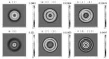
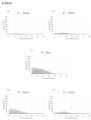
- FIG. It is a figure which shows the light intensity in the far field for every emission mode.
- FIG. 5 is a diagram showing light intensity in the far field for each emission mode classified and synthesized.
- FIG. 10 is a diagram showing the light intensity in the far field of light synthesized by changing the ratio for each light emission mode;
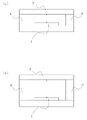
- 1 is a schematic plan view showing an optical element according to the present invention;
- FIG. It is a schematic sectional view showing a conventional optical system device. It is a figure which shows the light distribution in the far field of the irradiation part used for simulation.
- FIG. 4 is a diagram showing how light propagates from a lens used in Simulation 1;
- FIG. 4 is a diagram showing how light propagates from a lens used in Simulation 1;
- FIG. 4 is a diagram showing how light propagates from a lens used in Simulation 1;
- FIG. 4 is a diagram showing optical characteristics based on Simulation 1 (focal length of 20 ⁇ m); FIG. 4 is a diagram showing optical characteristics based on Simulation 1 (focal length of 40 ⁇ m); FIG. 4 is a diagram showing optical characteristics based on Simulation 1 (focal length of 60 ⁇ m);
- FIG. 10 is a diagram showing the state of light when parallel light is incident on the lens (focal length of 20 ⁇ m) used in Simulation 2;
- FIG. 10 is a diagram showing the state of light when parallel light is made incident on the lens (focal length of 40 ⁇ m) used in Simulation 2;
- FIG. 10 is a diagram showing a state of light when parallel light is incident on the lens (focal length of 60 ⁇ m) used in Simulation 2;
- FIG. 10 is a projection diagram due to a difference in ⁇ in Simulation 2 (focal length of 20 ⁇ m).
- FIG. 10 is a projection diagram due to a difference in ⁇ in Simulation 2 (focal length of 40 ⁇ m).
- FIG. 10 is a projection diagram due to a difference in ⁇ in Simulation 2 (focal length of 60 ⁇ m). It is a light distribution due to a difference in ⁇ in simulation 2 (focal length of 20 ⁇ m). It is a light distribution due to a difference in ⁇ in Simulation 2 (focal length of 40 ⁇ m). It is a light distribution due to a difference in ⁇ in simulation 2 (focal length of 60 ⁇ m).
- FIG. 10 is a projection diagram due to a difference in ⁇ in Simulation 2 (focal length of 20 ⁇ m).
- FIG. 10 is a projection diagram due to a difference in ⁇ in Simulation 2 (focal length of 40 ⁇ m).
- FIG. 10 is a diagram showing the maximum light intensity due to the difference in ⁇ in simulation 2 (focal length of 20 ⁇ m);
- FIG. 10 is a diagram showing the maximum light intensity depending on the difference in ⁇ in Simulation 2 (focal length of 40 ⁇ m);
- FIG. 10 is a diagram showing the maximum light intensity depending on the difference in ⁇ in simulation 2 (focal length of 60 ⁇ m); It is a figure explaining the lens of this invention.
- FIG. 11 is a diagram showing the state of light when parallel light is made incident on the lens used in Simulation 3;
- FIG. 10 is a projection diagram due to a difference in ⁇ in Simulation 3 (focal length of 20 ⁇ m). It is light distribution (x-axis direction) by the difference of (delta) in the simulation 3.
- FIG. 11 is a diagram showing the state of light when parallel light is made incident on the lens used in Simulation 3
- FIG. 10 is a projection diagram due to a difference in ⁇ in Simulation 3 (focal length of 20
- FIG. 10 is a diagram showing the maximum light intensity depending on the difference in ⁇ in simulation 3.
- FIG. 4 is a schematic plan view showing the positional relationship between an irradiation unit and an optical element according to the present invention;
- FIG. 4 is a schematic cross-sectional view showing another optical system device of the present invention;
- It is a schematic sectional view showing an optical system device as a diffuser of the present invention.
- 1 is a schematic cross-sectional view showing an optical system device having position adjusting means of the present invention;
- the optical system device of the present invention will be described below.
- the optical system device of the present invention is mainly composed of an irradiation section 1 for irradiating light of wavelength ⁇ and an optical element 2 having periodic lenses 21 .
- the irradiation unit 1 may be of any type as long as it has a light source that irradiates a plurality of lenses 21 with light of wavelength ⁇ . Also, the irradiation unit 1 may be a single light source or a plurality of light sources. Alternatively, a plurality of light sources may be provided by passing light from a single light source through an aperture formed with a plurality of pores. When the irradiation section is composed of a plurality of light sources, the light sources are preferably formed on the same plane.
- a specific example of the irradiation unit 1 is a VCSEL (Vertical Cavity Surface Emitting LASER) that is expected to produce high output with low power.
- a VCSEL has a plurality of light sources 10 capable of irradiating light in a direction perpendicular to a light emitting surface. Further, it is preferable to form a light absorption film on a portion other than the light source because noise due to reflected light does not enter.
- Flash mode Further, it is known that when the light intensity of a VCSEL is increased, the light of the VCSEL includes a plurality of light emission modes such as single mode and multimode. Examples of specific light emission modes are shown in FIG. Of the light emission modes shown in FIG. 2, (2) and (3), (4) and (6), (7) and (9), and (8) and (10), which are rotationally symmetrical to each other, always exist at the same rate. Therefore, by synthesizing these similar modes, they can be grouped into six types of A, B, C, D, E, and F as shown in FIG.
- the light source of the VCSEL has a higher proportion of light emission modes having the maximum intensity at the center of the optical axis among the light emission modes. It is preferable in that the light intensity can be increased and the contrast can be increased. Therefore, the ratio of the mode having the maximum intensity at the center of the optical axis among the emission modes of the light source should be 40% or more, preferably 45% or more, and more preferably 60% or more.
- the emission mode may be adjusted by a conventionally known method such as controlling the current injection path of the emission layer of the VCSEL.
- the optical element 2 is a periodic array of lenses 21 that transmit light of wavelength ⁇ .
- the lens 21 has a focal point at a predetermined distance f (f>0) from the lens 21 .
- the optical element of the present invention can improve the contrast more than the conventional one as the focal length f becomes larger such as 10 ⁇ m or more, 20 ⁇ m or more, 40 ⁇ m or more, or 60 ⁇ m or more.
- the shape of the lens 21 can be freely designed according to the spread pattern of the dots to be irradiated (hereinafter referred to as dot pattern).
- dot pattern For example, if the dot pattern is desired to be circular, the shape of the lens 21 should be a spherical lens. If the dot pattern is desired to be non-circular, the shape of the lens 21 should be an aspherical lens that is appropriately designed.
- Specific lens shapes include, for example, a convex lens, a concave lens, and a saddle-shaped lens that looks like a convex lens or a concave lens depending on the cross section.
- the periodic array includes a square array of square or rectangular lenses 21 in plan view as shown in FIG. are arranged in a hexagonal array.
- the lens 21 may be of any kind as long as it functions as a lens, and for example, a Fresnel lens, a DOE lens, a metalens, or the like can be used. Further, it is preferable that the lens 21 is formed with an antireflection film that prevents the light from the irradiation section from being reflected.
- the irradiation unit 1 and the optical element 2 are arranged so that the optical axis direction of the light source of the irradiation unit 1 and the optical axis direction of the lens 21 of the optical element 2 are aligned.
- n is a natural number of 1 or more
- ⁇ is the wavelength of light incident from the irradiation unit 1
- P is the pitch of the lens 21 of the optical element 2
- L0 is the distance between the irradiation unit 1 and the optical element 2. It has been thought that incident light can be converted into a high-contrast dot pattern when the distance L0 is represented by the following formula A (see FIG. 6).
- the focal length of the optical element is f
- the distance L 0 can be calculated by the following formula B
- the light is more strongly enhanced and a high-contrast dot pattern is produced.
- the light is most intensified when the following formula C is satisfied.
- the distance L1 between the irradiation section 1 and the focal position 9 of the optical element 2 is adjusted so as to satisfy Expression 1 for any two or more pitches Pk .
- diffraction is most affected by the smallest pitch, so it is better for the smallest pitch P 1 to satisfy Equation 1, and more preferably for the second smallest pitch P 2 also Equation 1 Better to fill
- the pitch Pk is too much smaller than the wavelength ⁇ of the light from the light source 10, it is difficult for diffraction to occur.
- the pitch P k especially the pitch P 1 , should be sufficiently larger than the wavelength ⁇ of the light from the light source 10, for example, 5 times or more, preferably 10 times or more.
- the distance L1 between the irradiation unit 1 and the focal position 9 of the optical element 2 is set to the following formula 3, and the light intensity distribution in the far field is simulated when ⁇ is changed variously.
- the lens 21 three types having a diameter of 30 ⁇ m, a refractive index of 1.5, and a focal length f of (a) 20 ⁇ m, (b) 40 ⁇ m, and (c) 60 ⁇ m were used.
- FIG. 8(a) is a diagram showing how light propagates when each lens is irradiated with parallel light as shown in FIG. 8(b).
- n in Formula 3 was set to 2.
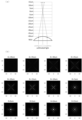
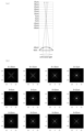
- 9 to 11 show the results of simulation using optical simulation software BeamPROP (manufactured by Synopsys). This simulation is a 2D calculation result that does not consider the depth direction in FIG. 2 for simplicity of calculation.
- the graphs of (a) of FIGS. 9 to 11 show the light intensity distribution when the distance L0 between the irradiation unit 1 and the optical element 2 satisfies the above-mentioned formula A as in the conventional art.
- Graphs in (b) of FIGS. 9 to 11 are light intensity distributions when the distance L1 between the irradiation unit 1 and the focal position 9 of the optical element 2 satisfies the above-mentioned formula 2.
- FIG. Graphs of (c) of FIGS. 9 to 11 show differences in the maximum light intensity of each light intensity distribution with respect to the value of ⁇ .
- the horizontal axis indicates the light distribution angle
- the vertical axis indicates the light intensity in the far field when the power of the light source is set to 1.
- the horizontal axis in (c) of FIGS. 9 to 11 indicates ⁇
- the vertical axis indicates the light intensity of the far field when the power of the light source is set to 1.
- the optical element 2 that satisfies the formula 1 has a clearer peak than the one that satisfies the formula A, and the peak light intensity is also higher. Also, it can be seen that the peak light intensity is maximized when Expression 2 is satisfied.
- the lens surface was rotationally symmetrical, with the same curvature in the x-axis direction and the y-axis direction.
- the lens 21 as shown in FIGS. 12 to 14, three types with focal lengths f of 20 ⁇ m, 40 ⁇ m and 60 ⁇ m were used.
- n in Formula 3 was set to 2.
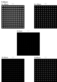
- 15 to 23 show the results of simulation using optical simulation software BeamPROP (manufactured by Synopsys). This simulation is a 3D calculation result in which the depth direction in FIG. 1 is also considered.
- 15 to 17 are projected images 50 cm ahead of the optical element when ⁇ in Equation 3 is varied in three types of lenses.
- 18 to 20 show light intensity distributions when ⁇ in Equation 3 is changed in various ways for three types of lenses.
- 21 to 23 show the maximum light intensity of each light intensity distribution with respect to the value of ⁇ for three types of lenses.
- the horizontal axis indicates the light distribution angle
- the vertical axis indicates the light intensity in the far field when the power of the light source is set to 1.
- the horizontal axis in (c) of FIGS. 18 to 20 indicates ⁇
- the vertical axis indicates the light intensity of the far field when the power of the light source is set to one.
- the optical element 2 that satisfies the formula 1 has a clearer peak than the one that satisfies the formula A, and the peak light intensity is also higher. Also, it can be seen that the peak light intensity is maximized when Expression 2 is satisfied.
- the shape of the lens 21 was a square with a side of 30 ⁇ m in plan view and a height of 16.26 ⁇ m, as shown in FIG. 24(a).
- the lens surface was a non-rotationally symmetrical aspherical surface with different curvatures in the x-axis direction and the y-axis direction.
- FIG. 24B is a projection diagram of the light distribution in the far field when parallel light is incident on the optical element.
- FIG. 24(c) shows the light distribution with respect to the angles in the x-axis direction and the y-axis direction in the far field.
- the focal length f of the lens 21 was 20 ⁇ m as shown in FIG.
- FIG. 25(b) is a projection view of emitted light when parallel light is incident on the lens 21.
- FIG. Although there is a difference in the way light is collected in the x-axis direction and the y-axis direction, the point where the light is most concentrated is the focal position (0 ⁇ m).
- n in Formula 3 is set to 2.
- 26 to 29 show the results of simulation using optical simulation software BeamPROP (manufactured by Synopsys). This simulation is a 3D calculation result in which the depth direction in FIG. 1 is also considered.
- FIG. 26 shows projected images 50 cm ahead from the optical element when ⁇ in Equation 3 is varied.
- FIG. 27 shows light intensity distributions in the x-axis direction when ⁇ in Equation 3 is varied.
- FIG. 28 shows light intensity distributions in the y-axis direction when ⁇ in Equation 3 is varied.
- FIG. 29 shows the maximum light intensity of each light intensity distribution in the x-axis direction and the y-axis direction with respect to the value of ⁇ .
- the horizontal axis indicates the light distribution angle
- the vertical axis indicates the light intensity in the far field when the power of the light source is set to 1.
- the horizontal axis indicates ⁇
- the vertical axis indicates the light intensity of the far field when the power of the light source is 1.
- the optical element 2 that satisfies the formula 3 has a clearer peak than the one that satisfies the formula A, and the peak light intensity is also higher.
- the position where the peak light intensity is maximized is different in the x-axis direction and the y-axis direction, but Equation 3 is satisfied. It can also be seen that there is sufficient light intensity if
- the lens 21 of the optical element 2 may be manufactured in any manner, but can be manufactured using, for example, an imprint method. Specifically, the material of the lens 21 is applied to the substrate 25 with a predetermined film thickness by a well-known method such as a spin coater (application step). Any material can be used as long as it can form the lens 21 that transmits light of wavelength ⁇ , and for example, polydimethylsiloxane (PDMS) can be used.
- PDMS polydimethylsiloxane
- a mold having a reverse pattern of the pattern in which the lenses 21 are arranged periodically is prepared, and the mold is pressed against the material coated on the substrate 25 to transfer the pattern (imprinting process).
- the irradiation unit 1 has a plurality of light sources 10, even if each light source 10 and the optical element 2 are relatively translated, the number of light sources 10 for each lens 21 of the optical element 2 is the same in plan view.
- the irradiating unit regularly illuminates a plurality of light sources m times or 1/m times the period in any of the periodic directions of the lens 21 of the optical element.
- the light sources 10 of the irradiation unit 1 are preferably arranged regularly at a pitch mPk or Pk /m in the direction in which the lenses 21 of the optical element 2 take the pitch Pk .
- the pitch mP 1 or P 1 /m is preferable.
- P 2 ⁇
- the distance L 1 between the irradiation unit 1 and the optical element 2 preferably satisfies the following formula 4, More preferably, the following formula 5 is satisfied.
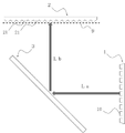
- the distance L1 between the irradiation unit 1 and the focal position 9 of the optical element 2 means a substantial distance (distance of the optical path). Therefore, the distance L1 in the case of FIG. 32 is La+Lb, which is the sum of the distance La from the irradiation unit 1 to the mirror 3 and the distance Lb from the mirror 3 to the focal position 9 of the optical element 2 indicated by the arrow. Thereby, the distance L can be adjusted using the mirror 3 . It is also possible to adjust the direction of the light from the light source.
- optical element 2 according to the present invention can be used not only for irradiating dot patterns, but also for diffuser applications.
- a first method of using the optical element 2 as a diffuser is, as shown in FIG. Prepare Part 6. Then, the distance L2 between the diffuser irradiation section 6 and the focal position 9 of the optical element 2 should not satisfy the formula (1). In other words, the distance L2 should satisfy the following expression ⁇ . As a result, as shown in the simulations 1 to 3 described above, it can be seen that the width of each peak is widened and the unevenness of the light intensity is reduced.
- the distance L 2 is the following formula ⁇ It is better to be close to
- the diffuser formed in this way can be used in combination with the above-described optical system for irradiating the dot pattern.
- the distance and shape of objects at a long distance can be measured by ensuring the intensity of the irradiation light by the dot pattern, and the distance and shape of objects at a short distance can be measured more accurately by irradiating the light of the diffuser. can be measured to
- the optical system device of the present invention may further include distance adjusting means 8 for adjusting the distance between the irradiation section 1 and the optical element 2, as shown in FIG. Thereby, the distance L1 between the irradiation unit 1 and the focal position 9 of the optical element 2 can be easily adjusted. Further, by adjusting the distance L1 between the irradiation unit 1 and the focal position 9 of the optical element 2, the optical system device of the present invention can be used by switching between dot pattern irradiation and diffuser irradiation. As the distance adjusting means 8, for example, a well-known actuator may be used.
Landscapes
- Physics & Mathematics (AREA)
- General Physics & Mathematics (AREA)
- Engineering & Computer Science (AREA)
- Optics & Photonics (AREA)
- Computer Networks & Wireless Communication (AREA)
- Radar, Positioning & Navigation (AREA)
- Remote Sensing (AREA)
- Optical Radar Systems And Details Thereof (AREA)
- Diffracting Gratings Or Hologram Optical Elements (AREA)
- Lenses (AREA)
Priority Applications (3)
| Application Number | Priority Date | Filing Date | Title |
|---|---|---|---|
| CN202280068218.3A CN118103738A (zh) | 2021-08-25 | 2022-08-19 | 光学系统装置 |
| EP22861275.0A EP4394458A4 (en) | 2021-08-25 | 2022-08-19 | OPTICAL SYSTEM DEVICE |
| JP2022563212A JP7418050B2 (ja) | 2021-08-25 | 2022-08-19 | 光学系装置 |
Applications Claiming Priority (2)
| Application Number | Priority Date | Filing Date | Title |
|---|---|---|---|
| JP2021-137560 | 2021-08-25 | ||
| JP2021137560 | 2021-08-25 |
Publications (1)
| Publication Number | Publication Date |
|---|---|
| WO2023026987A1 true WO2023026987A1 (ja) | 2023-03-02 |
Family
ID=85322146
Family Applications (1)
| Application Number | Title | Priority Date | Filing Date |
|---|---|---|---|
| PCT/JP2022/031411 Ceased WO2023026987A1 (ja) | 2021-08-25 | 2022-08-19 | 光学系装置 |
Country Status (4)
| Country | Link |
|---|---|
| EP (1) | EP4394458A4 (https=) |
| JP (1) | JP7418050B2 (https=) |
| CN (1) | CN118103738A (https=) |
| WO (1) | WO2023026987A1 (https=) |
Cited By (3)
| Publication number | Priority date | Publication date | Assignee | Title |
|---|---|---|---|---|
| WO2024029616A1 (ja) | 2022-08-05 | 2024-02-08 | Scivax株式会社 | 光学素子、光学系装置および光学系装置の製造方法 |
| WO2025057909A1 (ja) * | 2023-09-11 | 2025-03-20 | Scivax株式会社 | 光学系装置 |
| WO2025220552A1 (ja) * | 2024-04-16 | 2025-10-23 | Scivax株式会社 | 光学系装置 |
Families Citing this family (2)
| Publication number | Priority date | Publication date | Assignee | Title |
|---|---|---|---|---|
| WO2023090435A1 (ja) * | 2021-11-19 | 2023-05-25 | Scivax株式会社 | 光学系装置および光学素子製造方法 |
| CN115224583B (zh) * | 2022-06-21 | 2026-01-06 | 嘉兴驭光光电科技有限公司 | 基于微透镜阵列的激光投射模组 |
Citations (6)
| Publication number | Priority date | Publication date | Assignee | Title |
|---|---|---|---|---|
| JP2006500621A (ja) | 2002-09-20 | 2006-01-05 | コーニング・インコーポレーテッド | 光線成形及び均一化のためのランダムマイクロレンズアレイ |
| WO2017131585A1 (en) | 2016-01-26 | 2017-08-03 | Heptagon Micro Optics Pte. Ltd. | Multi-mode illumination module and related method |
| JP2018511034A (ja) * | 2015-01-29 | 2018-04-19 | ヘプタゴン・マイクロ・オプティクス・プライベート・リミテッドHeptagon Micro Optics Pte. Ltd. | パターン化された照射を生成するための装置 |
| WO2020222704A1 (en) * | 2019-04-29 | 2020-11-05 | Ams Sensors Asia Pte. Ltd. | Illumination apparatus |
| US11085609B1 (en) * | 2021-02-08 | 2021-08-10 | Himax Technologies Limited | Illumination device |
| WO2021230324A1 (ja) * | 2020-05-13 | 2021-11-18 | Scivax株式会社 | 光学系装置および光学素子製造方法 |
Family Cites Families (1)
| Publication number | Priority date | Publication date | Assignee | Title |
|---|---|---|---|---|
| CN115224583B (zh) * | 2022-06-21 | 2026-01-06 | 嘉兴驭光光电科技有限公司 | 基于微透镜阵列的激光投射模组 |
-
2022
- 2022-08-19 JP JP2022563212A patent/JP7418050B2/ja active Active
- 2022-08-19 EP EP22861275.0A patent/EP4394458A4/en active Pending
- 2022-08-19 CN CN202280068218.3A patent/CN118103738A/zh active Pending
- 2022-08-19 WO PCT/JP2022/031411 patent/WO2023026987A1/ja not_active Ceased
Patent Citations (7)
| Publication number | Priority date | Publication date | Assignee | Title |
|---|---|---|---|---|
| JP2006500621A (ja) | 2002-09-20 | 2006-01-05 | コーニング・インコーポレーテッド | 光線成形及び均一化のためのランダムマイクロレンズアレイ |
| JP2018511034A (ja) * | 2015-01-29 | 2018-04-19 | ヘプタゴン・マイクロ・オプティクス・プライベート・リミテッドHeptagon Micro Optics Pte. Ltd. | パターン化された照射を生成するための装置 |
| WO2017131585A1 (en) | 2016-01-26 | 2017-08-03 | Heptagon Micro Optics Pte. Ltd. | Multi-mode illumination module and related method |
| WO2020222704A1 (en) * | 2019-04-29 | 2020-11-05 | Ams Sensors Asia Pte. Ltd. | Illumination apparatus |
| WO2021230324A1 (ja) * | 2020-05-13 | 2021-11-18 | Scivax株式会社 | 光学系装置および光学素子製造方法 |
| WO2021229848A1 (ja) * | 2020-05-13 | 2021-11-18 | Scivax株式会社 | 光学系装置および光学素子製造方法 |
| US11085609B1 (en) * | 2021-02-08 | 2021-08-10 | Himax Technologies Limited | Illumination device |
Non-Patent Citations (1)
| Title |
|---|
| H. HAMAMLAU ARRAY, ILLUMINATOR, APPLIED OPTICS, vol. 43, no. 14, 10 May 2004 (2004-05-10), pages 2888 - 2894 |
Cited By (3)
| Publication number | Priority date | Publication date | Assignee | Title |
|---|---|---|---|---|
| WO2024029616A1 (ja) | 2022-08-05 | 2024-02-08 | Scivax株式会社 | 光学素子、光学系装置および光学系装置の製造方法 |
| WO2025057909A1 (ja) * | 2023-09-11 | 2025-03-20 | Scivax株式会社 | 光学系装置 |
| WO2025220552A1 (ja) * | 2024-04-16 | 2025-10-23 | Scivax株式会社 | 光学系装置 |
Also Published As
| Publication number | Publication date |
|---|---|
| EP4394458A4 (en) | 2025-08-20 |
| CN118103738A (zh) | 2024-05-28 |
| JP7418050B2 (ja) | 2024-01-19 |
| JPWO2023026987A1 (https=) | 2023-03-02 |
| EP4394458A1 (en) | 2024-07-03 |
Similar Documents
| Publication | Publication Date | Title |
|---|---|---|
| JP7418050B2 (ja) | 光学系装置 | |
| JP7061823B2 (ja) | 光学系装置および光学素子製造方法 | |
| JP7664440B2 (ja) | 光学系 | |
| CN104956179B (zh) | 利用折射或反射光的结构化元件从光源阵列生成结构化光场的光学系统 | |
| KR102026005B1 (ko) | 복합 확산판 | |
| JP7198341B2 (ja) | 構造高さを低くしたレーザー装置 | |
| US20230243482A1 (en) | Microstructures for Transforming Light Having Lambertian Distribution into Batwing Distributions | |
| KR20210118868A (ko) | 확산판 | |
| JP2020106771A (ja) | 回折光学素子およびこれを用いた光学系装置 | |
| JP7623743B2 (ja) | 光学系装置および光学素子製造方法 | |
| WO2024143433A1 (ja) | 光学系装置 | |
| WO2024106359A1 (ja) | 光学系装置および光学素子 | |
| CN120418679A (zh) | 光学系统装置 | |
| JP2024026011A (ja) | 光学系装置および光学素子製造方法 | |
| WO2025220552A1 (ja) | 光学系装置 | |
| TW202613650A (zh) | 光學系統裝置及光學元件 | |
| HK40068505B (zh) | 光学系统 | |
| US20250355146A1 (en) | Optical element and optical system device using same | |
| WO2026063418A1 (ja) | 光学系装置および光学素子 | |
| HK40029699B (zh) | 光学系统 |
Legal Events
| Date | Code | Title | Description |
|---|---|---|---|
| ENP | Entry into the national phase |
Ref document number: 2022563212 Country of ref document: JP Kind code of ref document: A |
|
| 121 | Ep: the epo has been informed by wipo that ep was designated in this application |
Ref document number: 22861275 Country of ref document: EP Kind code of ref document: A1 |
|
| WWE | Wipo information: entry into national phase |
Ref document number: 2022861275 Country of ref document: EP |
|
| NENP | Non-entry into the national phase |
Ref country code: DE |
|
| ENP | Entry into the national phase |
Ref document number: 2022861275 Country of ref document: EP Effective date: 20240325 |
|
| WWE | Wipo information: entry into national phase |
Ref document number: 202280068218.3 Country of ref document: CN |