WO2023026987A1 - Optical system device - Google Patents
Optical system device Download PDFInfo
- Publication number
- WO2023026987A1 WO2023026987A1 PCT/JP2022/031411 JP2022031411W WO2023026987A1 WO 2023026987 A1 WO2023026987 A1 WO 2023026987A1 JP 2022031411 W JP2022031411 W JP 2022031411W WO 2023026987 A1 WO2023026987 A1 WO 2023026987A1
- Authority
- WO
- WIPO (PCT)
- Prior art keywords
- light
- lens
- optical element
- distance
- irradiation unit
- Prior art date
Links
- 230000003287 optical effect Effects 0.000 title claims abstract description 97
- 230000001678 irradiating effect Effects 0.000 claims description 11
- 239000011295 pitch Substances 0.000 abstract description 39
- 238000004088 simulation Methods 0.000 description 36
- 238000009826 distribution Methods 0.000 description 24
- 238000010586 diagram Methods 0.000 description 20
- 238000000034 method Methods 0.000 description 9
- 238000004364 calculation method Methods 0.000 description 6
- 238000005259 measurement Methods 0.000 description 5
- 230000000737 periodic effect Effects 0.000 description 5
- 238000004519 manufacturing process Methods 0.000 description 3
- 239000000463 material Substances 0.000 description 3
- 238000009792 diffusion process Methods 0.000 description 2
- 239000004205 dimethyl polysiloxane Substances 0.000 description 2
- 229920000435 poly(dimethylsiloxane) Polymers 0.000 description 2
- 239000000758 substrate Substances 0.000 description 2
- 230000002194 synthesizing effect Effects 0.000 description 2
- 230000000694 effects Effects 0.000 description 1
- 238000005286 illumination Methods 0.000 description 1
- 238000002347 injection Methods 0.000 description 1
- 239000007924 injection Substances 0.000 description 1
- 230000031700 light absorption Effects 0.000 description 1
- -1 polydimethylsiloxane Polymers 0.000 description 1
- 239000011148 porous material Substances 0.000 description 1
Images


Classifications
-
- G—PHYSICS
- G01—MEASURING; TESTING
- G01S—RADIO DIRECTION-FINDING; RADIO NAVIGATION; DETERMINING DISTANCE OR VELOCITY BY USE OF RADIO WAVES; LOCATING OR PRESENCE-DETECTING BY USE OF THE REFLECTION OR RERADIATION OF RADIO WAVES; ANALOGOUS ARRANGEMENTS USING OTHER WAVES
- G01S7/00—Details of systems according to groups G01S13/00, G01S15/00, G01S17/00
- G01S7/48—Details of systems according to groups G01S13/00, G01S15/00, G01S17/00 of systems according to group G01S17/00
- G01S7/481—Constructional features, e.g. arrangements of optical elements
-
- G—PHYSICS
- G02—OPTICS
- G02B—OPTICAL ELEMENTS, SYSTEMS OR APPARATUS
- G02B3/00—Simple or compound lenses
- G02B3/0006—Arrays
- G02B3/0037—Arrays characterized by the distribution or form of lenses
- G02B3/0056—Arrays characterized by the distribution or form of lenses arranged along two different directions in a plane, e.g. honeycomb arrangement of lenses
-
- H—ELECTRICITY
- H01—ELECTRIC ELEMENTS
- H01S—DEVICES USING THE PROCESS OF LIGHT AMPLIFICATION BY STIMULATED EMISSION OF RADIATION [LASER] TO AMPLIFY OR GENERATE LIGHT; DEVICES USING STIMULATED EMISSION OF ELECTROMAGNETIC RADIATION IN WAVE RANGES OTHER THAN OPTICAL
- H01S5/00—Semiconductor lasers
- H01S5/005—Optical components external to the laser cavity, specially adapted therefor, e.g. for homogenisation or merging of the beams or for manipulating laser pulses, e.g. pulse shaping
-
- H—ELECTRICITY
- H01—ELECTRIC ELEMENTS
- H01S—DEVICES USING THE PROCESS OF LIGHT AMPLIFICATION BY STIMULATED EMISSION OF RADIATION [LASER] TO AMPLIFY OR GENERATE LIGHT; DEVICES USING STIMULATED EMISSION OF ELECTROMAGNETIC RADIATION IN WAVE RANGES OTHER THAN OPTICAL
- H01S5/00—Semiconductor lasers
- H01S5/40—Arrangement of two or more semiconductor lasers, not provided for in groups H01S5/02 - H01S5/30
- H01S5/42—Arrays of surface emitting lasers
- H01S5/423—Arrays of surface emitting lasers having a vertical cavity
Definitions
- the present invention relates to an optical system device.
- Three-dimensional measurement sensors using the time-of-flight (TOF) method are about to be adopted in mobile devices, cars, robots, etc. This measures the distance to an object from the time it takes for the light emitted from the light source to the object to be reflected and returned. If the light from the light source irradiates a predetermined area of the object uniformly, the distance at each irradiated point can be measured and the three-dimensional structure of the object can be detected.
- TOF time-of-flight
- the above sensor system consists of a light irradiation unit that irradiates the object with light, a camera unit that detects the light reflected from each point on the object, and a calculation unit that calculates the distance of the object from the signal received by the camera.
- the unique part of the above system is the light irradiation section consisting of a laser and an optical filter.
- a diffusion filter which shapes the beam by passing the laser light through a microlens array to provide uniform illumination of a controlled area on the target, is a distinctive component of the system.
- TOF has a need for long-distance measurement, and the intensity of the irradiated light must be strong enough to enable long-distance measurement.
- the randomly arranged microlens array is not suitable for long-distance measurement because the uniformity of the irradiated light is high and the intensity is low.
- Non-Patent Document 1 an optical system device using the Lau effect is known as a device that converts incident light into a dot pattern.
- This is composed of a diffraction grating with a predetermined pitch P and a light source. It is placed in A device in which the diffraction grating is replaced with a microlens is also being studied (for example, Patent Document 2).
- an object of the present invention is to provide an optical system device capable of irradiating high-contrast light.
- Another object of the present invention is to provide an optical system device that can be used as a diffuser for irradiating uniform light.
- an optical system device of the present invention has an optical element in which lenses that transmit light of wavelength ⁇ are arranged periodically, and a light source that irradiates a plurality of the lenses with light of wavelength ⁇ . and an irradiation unit, wherein f is the focal length of the lens, n is a natural number of 1 or more, and P is the size of the k-th smallest pitch of the lenses (k is a natural number of 1 or more). k , the distance L 1 between the irradiation unit and the focal position of the optical element for any one or more pitches P k is given by the following equation 1 is characterized by satisfying
- the distance L1 is expressed by the following formula 2 It is preferable to satisfy
- the smallest pitch P1 should preferably satisfy the above formula 1, and preferably the second smallest pitch P2 should also satisfy the above formula 1.
- another optical system device of the present invention includes an optical element in which lenses transmitting light of wavelength ⁇ are arranged periodically, an irradiation unit having a light source for irradiating a plurality of the lenses with light of wavelength ⁇ , and If f is the focal length of the lens, n is a natural number of 1 or more, and Pk is the size of the k-th smallest pitch of the lens (k is a natural number of 1 or more), any one of 1 or more With respect to the pitch Pk , the distance L2 between the irradiation unit and the focal position of the optical element is expressed by the following formula ⁇ is characterized by satisfying
- distance adjusting means for adjusting the distance between the optical element and the irradiation unit.
- the optical system device of the present invention can irradiate high-contrast light.
- FIG. 1 is a schematic cross-sectional view showing an optical system device of the present invention
- FIG. It is a figure which shows the light intensity in the far field for every emission mode.
- FIG. 5 is a diagram showing light intensity in the far field for each emission mode classified and synthesized.
- FIG. 10 is a diagram showing the light intensity in the far field of light synthesized by changing the ratio for each light emission mode;
- 1 is a schematic plan view showing an optical element according to the present invention;
- FIG. It is a schematic sectional view showing a conventional optical system device. It is a figure which shows the light distribution in the far field of the irradiation part used for simulation.
- FIG. 4 is a diagram showing how light propagates from a lens used in Simulation 1;
- FIG. 4 is a diagram showing how light propagates from a lens used in Simulation 1;
- FIG. 4 is a diagram showing how light propagates from a lens used in Simulation 1;
- FIG. 4 is a diagram showing optical characteristics based on Simulation 1 (focal length of 20 ⁇ m); FIG. 4 is a diagram showing optical characteristics based on Simulation 1 (focal length of 40 ⁇ m); FIG. 4 is a diagram showing optical characteristics based on Simulation 1 (focal length of 60 ⁇ m);
- FIG. 10 is a diagram showing the state of light when parallel light is incident on the lens (focal length of 20 ⁇ m) used in Simulation 2;
- FIG. 10 is a diagram showing the state of light when parallel light is made incident on the lens (focal length of 40 ⁇ m) used in Simulation 2;
- FIG. 10 is a diagram showing a state of light when parallel light is incident on the lens (focal length of 60 ⁇ m) used in Simulation 2;
- FIG. 10 is a projection diagram due to a difference in ⁇ in Simulation 2 (focal length of 20 ⁇ m).
- FIG. 10 is a projection diagram due to a difference in ⁇ in Simulation 2 (focal length of 40 ⁇ m).
- FIG. 10 is a projection diagram due to a difference in ⁇ in Simulation 2 (focal length of 60 ⁇ m). It is a light distribution due to a difference in ⁇ in simulation 2 (focal length of 20 ⁇ m). It is a light distribution due to a difference in ⁇ in Simulation 2 (focal length of 40 ⁇ m). It is a light distribution due to a difference in ⁇ in simulation 2 (focal length of 60 ⁇ m).
- FIG. 10 is a projection diagram due to a difference in ⁇ in Simulation 2 (focal length of 20 ⁇ m).
- FIG. 10 is a projection diagram due to a difference in ⁇ in Simulation 2 (focal length of 40 ⁇ m).
- FIG. 10 is a diagram showing the maximum light intensity due to the difference in ⁇ in simulation 2 (focal length of 20 ⁇ m);
- FIG. 10 is a diagram showing the maximum light intensity depending on the difference in ⁇ in Simulation 2 (focal length of 40 ⁇ m);
- FIG. 10 is a diagram showing the maximum light intensity depending on the difference in ⁇ in simulation 2 (focal length of 60 ⁇ m); It is a figure explaining the lens of this invention.
- FIG. 11 is a diagram showing the state of light when parallel light is made incident on the lens used in Simulation 3;
- FIG. 10 is a projection diagram due to a difference in ⁇ in Simulation 3 (focal length of 20 ⁇ m). It is light distribution (x-axis direction) by the difference of (delta) in the simulation 3.
- FIG. 11 is a diagram showing the state of light when parallel light is made incident on the lens used in Simulation 3
- FIG. 10 is a projection diagram due to a difference in ⁇ in Simulation 3 (focal length of 20
- FIG. 10 is a diagram showing the maximum light intensity depending on the difference in ⁇ in simulation 3.
- FIG. 4 is a schematic plan view showing the positional relationship between an irradiation unit and an optical element according to the present invention;
- FIG. 4 is a schematic cross-sectional view showing another optical system device of the present invention;
- It is a schematic sectional view showing an optical system device as a diffuser of the present invention.
- 1 is a schematic cross-sectional view showing an optical system device having position adjusting means of the present invention;
- the optical system device of the present invention will be described below.
- the optical system device of the present invention is mainly composed of an irradiation section 1 for irradiating light of wavelength ⁇ and an optical element 2 having periodic lenses 21 .
- the irradiation unit 1 may be of any type as long as it has a light source that irradiates a plurality of lenses 21 with light of wavelength ⁇ . Also, the irradiation unit 1 may be a single light source or a plurality of light sources. Alternatively, a plurality of light sources may be provided by passing light from a single light source through an aperture formed with a plurality of pores. When the irradiation section is composed of a plurality of light sources, the light sources are preferably formed on the same plane.
- a specific example of the irradiation unit 1 is a VCSEL (Vertical Cavity Surface Emitting LASER) that is expected to produce high output with low power.
- a VCSEL has a plurality of light sources 10 capable of irradiating light in a direction perpendicular to a light emitting surface. Further, it is preferable to form a light absorption film on a portion other than the light source because noise due to reflected light does not enter.
- Flash mode Further, it is known that when the light intensity of a VCSEL is increased, the light of the VCSEL includes a plurality of light emission modes such as single mode and multimode. Examples of specific light emission modes are shown in FIG. Of the light emission modes shown in FIG. 2, (2) and (3), (4) and (6), (7) and (9), and (8) and (10), which are rotationally symmetrical to each other, always exist at the same rate. Therefore, by synthesizing these similar modes, they can be grouped into six types of A, B, C, D, E, and F as shown in FIG.
- the light source of the VCSEL has a higher proportion of light emission modes having the maximum intensity at the center of the optical axis among the light emission modes. It is preferable in that the light intensity can be increased and the contrast can be increased. Therefore, the ratio of the mode having the maximum intensity at the center of the optical axis among the emission modes of the light source should be 40% or more, preferably 45% or more, and more preferably 60% or more.
- the emission mode may be adjusted by a conventionally known method such as controlling the current injection path of the emission layer of the VCSEL.
- the optical element 2 is a periodic array of lenses 21 that transmit light of wavelength ⁇ .
- the lens 21 has a focal point at a predetermined distance f (f>0) from the lens 21 .
- the optical element of the present invention can improve the contrast more than the conventional one as the focal length f becomes larger such as 10 ⁇ m or more, 20 ⁇ m or more, 40 ⁇ m or more, or 60 ⁇ m or more.
- the shape of the lens 21 can be freely designed according to the spread pattern of the dots to be irradiated (hereinafter referred to as dot pattern).
- dot pattern For example, if the dot pattern is desired to be circular, the shape of the lens 21 should be a spherical lens. If the dot pattern is desired to be non-circular, the shape of the lens 21 should be an aspherical lens that is appropriately designed.
- Specific lens shapes include, for example, a convex lens, a concave lens, and a saddle-shaped lens that looks like a convex lens or a concave lens depending on the cross section.
- the periodic array includes a square array of square or rectangular lenses 21 in plan view as shown in FIG. are arranged in a hexagonal array.
- the lens 21 may be of any kind as long as it functions as a lens, and for example, a Fresnel lens, a DOE lens, a metalens, or the like can be used. Further, it is preferable that the lens 21 is formed with an antireflection film that prevents the light from the irradiation section from being reflected.
- the irradiation unit 1 and the optical element 2 are arranged so that the optical axis direction of the light source of the irradiation unit 1 and the optical axis direction of the lens 21 of the optical element 2 are aligned.
- n is a natural number of 1 or more
- ⁇ is the wavelength of light incident from the irradiation unit 1
- P is the pitch of the lens 21 of the optical element 2
- L0 is the distance between the irradiation unit 1 and the optical element 2. It has been thought that incident light can be converted into a high-contrast dot pattern when the distance L0 is represented by the following formula A (see FIG. 6).
- the focal length of the optical element is f
- the distance L 0 can be calculated by the following formula B
- the light is more strongly enhanced and a high-contrast dot pattern is produced.
- the light is most intensified when the following formula C is satisfied.
- the distance L1 between the irradiation section 1 and the focal position 9 of the optical element 2 is adjusted so as to satisfy Expression 1 for any two or more pitches Pk .
- diffraction is most affected by the smallest pitch, so it is better for the smallest pitch P 1 to satisfy Equation 1, and more preferably for the second smallest pitch P 2 also Equation 1 Better to fill
- the pitch Pk is too much smaller than the wavelength ⁇ of the light from the light source 10, it is difficult for diffraction to occur.
- the pitch P k especially the pitch P 1 , should be sufficiently larger than the wavelength ⁇ of the light from the light source 10, for example, 5 times or more, preferably 10 times or more.
- the distance L1 between the irradiation unit 1 and the focal position 9 of the optical element 2 is set to the following formula 3, and the light intensity distribution in the far field is simulated when ⁇ is changed variously.
- the lens 21 three types having a diameter of 30 ⁇ m, a refractive index of 1.5, and a focal length f of (a) 20 ⁇ m, (b) 40 ⁇ m, and (c) 60 ⁇ m were used.
- FIG. 8(a) is a diagram showing how light propagates when each lens is irradiated with parallel light as shown in FIG. 8(b).
- n in Formula 3 was set to 2.
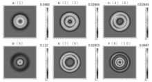
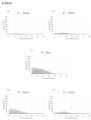
- 9 to 11 show the results of simulation using optical simulation software BeamPROP (manufactured by Synopsys). This simulation is a 2D calculation result that does not consider the depth direction in FIG. 2 for simplicity of calculation.
- the graphs of (a) of FIGS. 9 to 11 show the light intensity distribution when the distance L0 between the irradiation unit 1 and the optical element 2 satisfies the above-mentioned formula A as in the conventional art.
- Graphs in (b) of FIGS. 9 to 11 are light intensity distributions when the distance L1 between the irradiation unit 1 and the focal position 9 of the optical element 2 satisfies the above-mentioned formula 2.
- FIG. Graphs of (c) of FIGS. 9 to 11 show differences in the maximum light intensity of each light intensity distribution with respect to the value of ⁇ .
- the horizontal axis indicates the light distribution angle
- the vertical axis indicates the light intensity in the far field when the power of the light source is set to 1.
- the horizontal axis in (c) of FIGS. 9 to 11 indicates ⁇
- the vertical axis indicates the light intensity of the far field when the power of the light source is set to 1.
- the optical element 2 that satisfies the formula 1 has a clearer peak than the one that satisfies the formula A, and the peak light intensity is also higher. Also, it can be seen that the peak light intensity is maximized when Expression 2 is satisfied.
- the lens surface was rotationally symmetrical, with the same curvature in the x-axis direction and the y-axis direction.
- the lens 21 as shown in FIGS. 12 to 14, three types with focal lengths f of 20 ⁇ m, 40 ⁇ m and 60 ⁇ m were used.
- n in Formula 3 was set to 2.
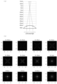
- 15 to 23 show the results of simulation using optical simulation software BeamPROP (manufactured by Synopsys). This simulation is a 3D calculation result in which the depth direction in FIG. 1 is also considered.
- 15 to 17 are projected images 50 cm ahead of the optical element when ⁇ in Equation 3 is varied in three types of lenses.
- 18 to 20 show light intensity distributions when ⁇ in Equation 3 is changed in various ways for three types of lenses.
- 21 to 23 show the maximum light intensity of each light intensity distribution with respect to the value of ⁇ for three types of lenses.
- the horizontal axis indicates the light distribution angle
- the vertical axis indicates the light intensity in the far field when the power of the light source is set to 1.
- the horizontal axis in (c) of FIGS. 18 to 20 indicates ⁇
- the vertical axis indicates the light intensity of the far field when the power of the light source is set to one.
- the optical element 2 that satisfies the formula 1 has a clearer peak than the one that satisfies the formula A, and the peak light intensity is also higher. Also, it can be seen that the peak light intensity is maximized when Expression 2 is satisfied.
- the shape of the lens 21 was a square with a side of 30 ⁇ m in plan view and a height of 16.26 ⁇ m, as shown in FIG. 24(a).
- the lens surface was a non-rotationally symmetrical aspherical surface with different curvatures in the x-axis direction and the y-axis direction.
- FIG. 24B is a projection diagram of the light distribution in the far field when parallel light is incident on the optical element.
- FIG. 24(c) shows the light distribution with respect to the angles in the x-axis direction and the y-axis direction in the far field.
- the focal length f of the lens 21 was 20 ⁇ m as shown in FIG.
- FIG. 25(b) is a projection view of emitted light when parallel light is incident on the lens 21.
- FIG. Although there is a difference in the way light is collected in the x-axis direction and the y-axis direction, the point where the light is most concentrated is the focal position (0 ⁇ m).
- n in Formula 3 is set to 2.
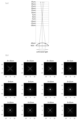
- 26 to 29 show the results of simulation using optical simulation software BeamPROP (manufactured by Synopsys). This simulation is a 3D calculation result in which the depth direction in FIG. 1 is also considered.
- FIG. 26 shows projected images 50 cm ahead from the optical element when ⁇ in Equation 3 is varied.
- FIG. 27 shows light intensity distributions in the x-axis direction when ⁇ in Equation 3 is varied.
- FIG. 28 shows light intensity distributions in the y-axis direction when ⁇ in Equation 3 is varied.
- FIG. 29 shows the maximum light intensity of each light intensity distribution in the x-axis direction and the y-axis direction with respect to the value of ⁇ .
- the horizontal axis indicates the light distribution angle
- the vertical axis indicates the light intensity in the far field when the power of the light source is set to 1.
- the horizontal axis indicates ⁇
- the vertical axis indicates the light intensity of the far field when the power of the light source is 1.
- the optical element 2 that satisfies the formula 3 has a clearer peak than the one that satisfies the formula A, and the peak light intensity is also higher.
- the position where the peak light intensity is maximized is different in the x-axis direction and the y-axis direction, but Equation 3 is satisfied. It can also be seen that there is sufficient light intensity if
- the lens 21 of the optical element 2 may be manufactured in any manner, but can be manufactured using, for example, an imprint method. Specifically, the material of the lens 21 is applied to the substrate 25 with a predetermined film thickness by a well-known method such as a spin coater (application step). Any material can be used as long as it can form the lens 21 that transmits light of wavelength ⁇ , and for example, polydimethylsiloxane (PDMS) can be used.
- PDMS polydimethylsiloxane
- a mold having a reverse pattern of the pattern in which the lenses 21 are arranged periodically is prepared, and the mold is pressed against the material coated on the substrate 25 to transfer the pattern (imprinting process).
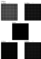
- the irradiation unit 1 has a plurality of light sources 10, even if each light source 10 and the optical element 2 are relatively translated, the number of light sources 10 for each lens 21 of the optical element 2 is the same in plan view.
- the irradiating unit regularly illuminates a plurality of light sources m times or 1/m times the period in any of the periodic directions of the lens 21 of the optical element.
- the light sources 10 of the irradiation unit 1 are preferably arranged regularly at a pitch mPk or Pk /m in the direction in which the lenses 21 of the optical element 2 take the pitch Pk .
- the pitch mP 1 or P 1 /m is preferable.
- P 2 ⁇
- the distance L 1 between the irradiation unit 1 and the optical element 2 preferably satisfies the following formula 4, More preferably, the following formula 5 is satisfied.
- the distance L1 between the irradiation unit 1 and the focal position 9 of the optical element 2 means a substantial distance (distance of the optical path). Therefore, the distance L1 in the case of FIG. 32 is La+Lb, which is the sum of the distance La from the irradiation unit 1 to the mirror 3 and the distance Lb from the mirror 3 to the focal position 9 of the optical element 2 indicated by the arrow. Thereby, the distance L can be adjusted using the mirror 3 . It is also possible to adjust the direction of the light from the light source.
- optical element 2 according to the present invention can be used not only for irradiating dot patterns, but also for diffuser applications.
- a first method of using the optical element 2 as a diffuser is, as shown in FIG. Prepare Part 6. Then, the distance L2 between the diffuser irradiation section 6 and the focal position 9 of the optical element 2 should not satisfy the formula (1). In other words, the distance L2 should satisfy the following expression ⁇ . As a result, as shown in the simulations 1 to 3 described above, it can be seen that the width of each peak is widened and the unevenness of the light intensity is reduced.
- the distance L 2 is the following formula ⁇ It is better to be close to
- the diffuser formed in this way can be used in combination with the above-described optical system for irradiating the dot pattern.
- the distance and shape of objects at a long distance can be measured by ensuring the intensity of the irradiation light by the dot pattern, and the distance and shape of objects at a short distance can be measured more accurately by irradiating the light of the diffuser. can be measured to
- the optical system device of the present invention may further include distance adjusting means 8 for adjusting the distance between the irradiation section 1 and the optical element 2, as shown in FIG. Thereby, the distance L1 between the irradiation unit 1 and the focal position 9 of the optical element 2 can be easily adjusted. Further, by adjusting the distance L1 between the irradiation unit 1 and the focal position 9 of the optical element 2, the optical system device of the present invention can be used by switching between dot pattern irradiation and diffuser irradiation. As the distance adjusting means 8, for example, a well-known actuator may be used.
Landscapes
- Physics & Mathematics (AREA)
- General Physics & Mathematics (AREA)
- Engineering & Computer Science (AREA)
- Optics & Photonics (AREA)
- Computer Networks & Wireless Communication (AREA)
- Radar, Positioning & Navigation (AREA)
- Remote Sensing (AREA)
- Diffracting Gratings Or Hologram Optical Elements (AREA)
- Lenses (AREA)
Abstract
Description
本発明は、光学系装置に関するものである。 The present invention relates to an optical system device.
タイムオブフライト(TOF)法を用いた3次元計測センサが携帯機器、車、ロボット等に採用されようとしている。これは、光源から対象物に照射された光が反射され戻って来るまでの時間から対象物の距離を計測するものである。光源からの光が対象物の所定の領域に均一に照射されていれば、照射されている各点における距離を測定でき対象物の立体構造が検知できることになる。 Three-dimensional measurement sensors using the time-of-flight (TOF) method are about to be adopted in mobile devices, cars, robots, etc. This measures the distance to an object from the time it takes for the light emitted from the light source to the object to be reflected and returned. If the light from the light source irradiates a predetermined area of the object uniformly, the distance at each irradiated point can be measured and the three-dimensional structure of the object can be detected.
上記センサーシステムは対象物に光を照射する光照射部と対象物の各点から反射してきた光を検知するカメラ部及びカメラが受光した信号から対象物の距離を算出する演算部からなる。 The above sensor system consists of a light irradiation unit that irradiates the object with light, a camera unit that detects the light reflected from each point on the object, and a calculation unit that calculates the distance of the object from the signal received by the camera.
カメラ部と演算部は既存のCMOSイメージャとCPUを使用できるため、上記システムの独自の部分はレーザと光学フィルタからなる光照射部となる。特にマイクロレンズアレイにレーザ光を透過させることでビームを整形し、対象物に対して制御された領域での均一な照射を行う拡散フィルタは、上記システムの特徴的な部品となる。 Since the existing CMOS imager and CPU can be used for the camera section and calculation section, the unique part of the above system is the light irradiation section consisting of a laser and an optical filter. In particular, a diffusion filter, which shapes the beam by passing the laser light through a microlens array to provide uniform illumination of a controlled area on the target, is a distinctive component of the system.
ここで、従来の拡散フィルタは、マイクロレンズアレイが周期構造であるために、回折の影響で光強度のむらが生じるという問題があった。そこで、このむらを抑制するために、各レンズをランダムに配置する等の工夫が行われている(例えば、特許文献1)。 Here, conventional diffusion filters have a problem that light intensity unevenness occurs due to the influence of diffraction because the microlens array has a periodic structure. Therefore, in order to suppress this unevenness, measures such as arranging each lens at random have been made (for example, Patent Document 1).
一方、TOFには、遠距離測定のニーズがあり、照射光のインテンシティには、遠距離測定ができるだけの強さが必要となる。しかし、ランダムに配置したマイクロレンズアレイは照射光の均一性が高い分、インテンシティが低くなるため、遠距離測定には不向きである。 On the other hand, TOF has a need for long-distance measurement, and the intensity of the irradiated light must be strong enough to enable long-distance measurement. However, the randomly arranged microlens array is not suitable for long-distance measurement because the uniformity of the irradiated light is high and the intensity is low.
そこで、電力を節減しなおかつ強い光の信号を処理できる方法としてドットパターンを照射し、この光のタイムオブフライトから3次元計測を行うことが検討されている。 Therefore, as a method that can save power and process strong light signals, it is being studied to irradiate a dot pattern and perform three-dimensional measurement from the time-of-flight of this light.
従来、入射した光をドットパターンに変換するものとしては、Lau効果を利用した光学系装置が知られている(例えば、非特許文献1)。これは、所定ピッチPの回折格子と光源で構成されるもので、光源の光の波長をλ、nを1以上の自然数とすると、回折格子と光源の距離L0が下記式Aを満たすように配置したものである。

しかしながら、回折格子をマイクロレンズに置き換えたものでは、ドットパターンのコントラストが低いという問題があった。 However, when the diffraction grating is replaced with microlenses, there is a problem that the contrast of the dot pattern is low.
そこで本発明は、コントラストの高い光を照射することができる光学系装置を提供することを目的とする。また、逆に均一な光を照射するためのディフューザとして利用可能な光学系装置を提供することを目的とする。 Accordingly, an object of the present invention is to provide an optical system device capable of irradiating high-contrast light. Another object of the present invention is to provide an optical system device that can be used as a diffuser for irradiating uniform light.
上記目的を達成するために、本発明の光学系装置は、波長λの光を透過するレンズが周期的に配列された光学素子と、波長λの光を前記レンズの複数に照射する光源を有する照射部と、を具備し、前記レンズの焦点距離をf、nを1以上の自然数とし、前記レンズのピッチのうち小さいものからk番目(kは1以上の自然数)のピッチの大きさをPkとすると、いずれか1以上のピッチPkについて、前記照射部と前記光学素子の焦点位置との距離L1が、下記式1

この場合、前記距離L1が、下記式2

また、最も小さいピッチP1について、前記式1を満たす方がよく、好ましくは、2番目に小さいピッチP2についても、前記式1を満たす方がよい。
Also, the smallest pitch P1 should preferably satisfy the
また、本発明の別の光学系装置は、波長λの光を透過するレンズが周期的に配列された光学素子と、波長λの光を前記レンズの複数に照射する光源を有する照射部と、を具備し、
前記レンズの焦点距離をf、nを1以上の自然数とし、前記レンズのピッチのうち小さいものからk番目(kは1以上の自然数)のピッチの大きさをPkとすると、いずれか1以上のピッチPkについて、前記照射部と前記光学素子の焦点位置との距離L2が、下記式α

If f is the focal length of the lens, n is a natural number of 1 or more, and Pk is the size of the k-th smallest pitch of the lens (k is a natural number of 1 or more), any one of 1 or more With respect to the pitch Pk , the distance L2 between the irradiation unit and the focal position of the optical element is expressed by the following formula α
また、前記光学素子と前記照射部の距離を調節する距離調節手段を具備する方が好ましい。 Further, it is preferable to provide distance adjusting means for adjusting the distance between the optical element and the irradiation unit.
本発明の光学系装置は、コントラストの高い光を照射することができる。 The optical system device of the present invention can irradiate high-contrast light.
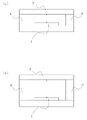
以下に、本発明の光学系装置について説明する。本発明の光学系装置は、図1に示すように、波長λの光を照射する照射部1と、周期的なレンズ21を有する光学素子2と、で主に構成される。
The optical system device of the present invention will be described below. The optical system device of the present invention, as shown in FIG. 1, is mainly composed of an
照射部1は、波長λの光をレンズ21の複数に照射する光源を有するものであればどのようなものでもよい。また、照射部1は、単光源でも複数光源でもよい。また、単光源の光を複数の細孔が形成されたアパーチャーに通すことにより複数光源としたものでもよい。照射部を複数光源で構成する場合には、当該光源は、同一平面上に形成される方が好ましい。照射部1の具体例としては、例えば、少ない電力で高出力が見込めるVCSEL(Vertical Cavity Surface Emitting LASER)を挙げることができる。VCSELは、発光面に垂直な方向に光を照射することができる光源10を複数有するものである。また、光源以外の部分に光吸収膜が形成されている方が反射光によるノイズが入らないため好ましい。
The
[発光モード]
また、VCSELの光強度を大きくする場合、当該VCSELの光には、シングルモードやマルチモード等の複数の発光モードが含まれることが知られている。具体的な発光モードの例を図2に示す。図2に示す発光モードのうち互いに回転対称である(2)と(3)、(4)と(6)、(7)と(9)、(8)と(10)は、必ず同率で存在するため、これらの類似モードをそれぞれ合成すると図3に示すようにA、B、C、D、E、Fの6種類に集約できる。
[Flash mode]
Further, it is known that when the light intensity of a VCSEL is increased, the light of the VCSEL includes a plurality of light emission modes such as single mode and multimode. Examples of specific light emission modes are shown in FIG. Of the light emission modes shown in FIG. 2, (2) and (3), (4) and (6), (7) and (9), and (8) and (10), which are rotationally symmetrical to each other, always exist at the same rate. Therefore, by synthesizing these similar modes, they can be grouped into six types of A, B, C, D, E, and F as shown in FIG.
これら6種類のモードを同じ割合(A:B:C:D:E:F=1:1:1:1:1:1)で合成すると図4(a)に示すようになり、最大強度は0.0271となる。なお、図は、光源のパワーを1としたときの各配光角における遠方界の光強度である。
一方、これら6種類のモードを1種類だけその他のモードの2倍にして合成すると図4(b)に示すように、A:B:C:D:E:F=2:1:1:1:1:1は、最大強度が0.03、A:B:C:D:E:F=1:1:1:2:1:1は、最大強度が0.0389、A:B:C:D:E:F=1:1:1:1:1:2は、最大強度が0.0285となる。すなわち、各モードのうち、最大強度が光軸中心にあるモードA又はD、または、最大強度が光軸中心に近いモードFの割合が増えると、6種類のモードを同じ割合にした場合に比べて、合成後の光の最大強度が大きくなることがわかる。図4(c)は、6種類のモードのうち、更に、モードA、モードD、モードFだけをその他のモードの5倍にして合成したものである。A:B:C:D:E:F=5:1:1:1:1:1は、最大強度が0.0354、A:B:C:D:E:F=1:1:1:5:1:1は、最大強度が0.0608、A:B:C:D:E:F=1:1:1:1:1:5は、最大強度が0.0343となった。すなわち、モードDを5倍にして合成した光(A:B:C:D:E:F=1:1:1:5:1:1)は、特に顕著に合成後の光の最大強度が大きくなった。
Combining these six modes at the same ratio (A:B:C:D:E:F=1:1:1:1:1:1) results in the result shown in FIG. 0.0271. The figure shows the light intensity of the far field at each light distribution angle when the power of the light source is 1. FIG.
On the other hand, if one of these six types of modes is doubled from the other modes and synthesized, A:B:C:D:E:F=2:1:1:1 as shown in FIG. 4(b). :1:1 has a maximum strength of 0.03, A:B:C:D:E:F=1:1:1:2:1:1 has a maximum strength of 0.0389, A:B:C :D:E:F=1:1:1:1:1:2 gives a maximum intensity of 0.0285. That is, when the proportion of mode A or D, whose maximum intensity is at the center of the optical axis, or mode F, whose maximum intensity is near the center of the optical axis, increases, compared to the case where the proportions of the six modes are the same. It can be seen that the maximum intensity of the combined light increases as the number increases. FIG. 4(c) is obtained by synthesizing only mode A, mode D, and mode F out of the six types of modes by multiplying the other modes by 5 times. A:B:C:D:E:F=5:1:1:1:1:1 has a maximum intensity of 0.0354, A:B:C:D:E:F=1:1:1: 5:1:1 has a maximum intensity of 0.0608, and A:B:C:D:E:F=1:1:1:1:1:5 has a maximum intensity of 0.0343. That is, the combined light (A:B:C:D:E:F=1:1:1:5:1:1) obtained by multiplying the mode D by 5 has a particularly remarkable maximum intensity of the combined light. got bigger.
以上のことから、複数の発光モードを有するVCSELを用いる場合には、当該VCSELの光源は、発光モードのうち光軸中心に最大強度を有する発光モードの割合が多い方が、生成されるドットの光強度を大きくすることができ、コントラストも大きくできる点で好ましい。したがって、光源の発光モードのうち光軸中心に最大強度を有するモードの割合は、40%以上、好ましくは45%以上、更に好ましくは60%以上である方がよい。当該発光モードは、VCSELの発光層の電流注入経路をコントロールする等、従来から知られている方法で調整すればよい。 From the above, when a VCSEL having a plurality of light emission modes is used, the light source of the VCSEL has a higher proportion of light emission modes having the maximum intensity at the center of the optical axis among the light emission modes. It is preferable in that the light intensity can be increased and the contrast can be increased. Therefore, the ratio of the mode having the maximum intensity at the center of the optical axis among the emission modes of the light source should be 40% or more, preferably 45% or more, and more preferably 60% or more. The emission mode may be adjusted by a conventionally known method such as controlling the current injection path of the emission layer of the VCSEL.
光学素子2は、波長λの光を透過するレンズ21が周期的に配列されたものである。ここでレンズ21とは、レンズ21から所定の距離f(f>0)離れた位置に焦点を有するものである。本発明の光学素子は、焦点距離fが10μm以上、20μm以上、40μm以上、60μm以上のように大きくなる程、従来のものよりコントラストを向上することができる。
The
レンズ21の形状は、照射したいドットの広がり方のパターン(以下、ドットパターンという)に合わせて自由に設計することができる。たとえば、ドットパターンを円状にしたい場合には、レンズ21の形状を球面レンズにすればよい。また、ドットパターンを非円形にしたい場合には、レンズ21の形状を適切に設計した非球面レンズにすればよい。具体的なレンズ形状としては、例えば、凸レンズや凹レンズの他、断面によって凸レンズや凹レンズに見えるサドル型のレンズなどがある。また、周期配列には、図5(a)に示すような平面視で正方形や長方形のレンズ21を正方配列にするものや、図5(b)に示すような平面視で六角形のレンズ21を六方配列にするものなどが該当する。また、レンズ21は、レンズとして機能すればどのようなものでもよく、例えば、フレネルレンズやDOEレンズ、メタレンズ等を用いることもできる。また、レンズ21には、照射部からの光が反射するのを防止する反射防止膜が形成されている方が好ましい。
The shape of the
照射部1と光学素子2は、照射部1の光源の光軸方向と光学素子2のレンズ21の光軸方向が一致するように配置される。
The
[照射部と光学素子の位置関係]
従来、nを1以上の自然数とし、照射部1から入射する光の波長をλ、光学素子2のレンズ21のピッチをP、照射部1と光学素子2の間の距離をL0とすると、距離L0が下記式Aの場合に入射した光をコントラストの大きなドットパターンに変換できると考えられてきた(図6参照)。

Conventionally, n is a natural number of 1 or more, λ is the wavelength of light incident from the
しかしながら、本発明者等が鋭意研究した結果、光学素子の焦点距離をfとすると、距離L0は、下記式B


式B、式Cを、照射部1と光学素子2の間の距離L0ではなく、図1に示すように、照射部1と光学素子2の焦点位置9との距離L1(L1=L0-f)で表すと、下記式D、式Eとなる。


また、レンズ21には、周期が複数存在する場合がある。例えば、図5(a)に示すように、平面視で正方形のレンズ21を正方配列にした場合には、隣り合うレンズとのピッチP1の他、対角線方向のピッチP2(=√2P1)や、ピッチP3(=√5P1)等種々のピッチが存在する。また、図2(b)に示すように、平面視で正六角形のレンズ21を六方配列にした場合には、隣り合うレンズとのピッチP1の他、ピッチP2(=√3P1)等が存在する。また、平面視で長方形のレンズを規則的に配列する場合のように、レンズ21が異なる周期を複数有する場合もある。この場合には、レンズ21のピッチのうち小さいものからk番目(kは1以上の自然数)のピッチの大きさをPk、係数をa(a≦1)、b(b≦1)とすると、いずれか1以上のピッチPkについて、照射部と光学素子の焦点位置9との距離L1が、下記式F

ここで式Fの係数aはa=1、a=0.5、a=0.3、a=0.1と小さい程好ましい。また、係数bもb=1、b=0.5、b=0.3、b=0.1と小さい程好ましい。式Fの係数が、a=1、b=1の場合、式Fは下記式1となる。

また、距離L1は、a=b=0である下記式2を満たす場合が最も好ましい。

なお、好ましくは、いずれか2以上のピッチPkについて、式1を満たすように、照射部1と光学素子2の焦点位置9との距離L1を調節する方がよい。その場合、回折は、ピッチが最も小さいものの影響が最も大きくなるため、最も小さいピッチP1について、式1を満たす方がよく、更に好ましくは、2番目に小さいピッチP2についても、式1を満たす方がよい。
Preferably, the distance L1 between the
なお、ピッチPkが光源10の光の波長λより小さくなり過ぎると回折を生じ難くなるため、光源10の配光角内に回折を生じるのに十分なレンズ21が含まれている限りにおいて、ピッチPk、特にピッチP1は、光源10の光の波長λより十分に大きい方がよく、例えば5倍以上、好ましくは10倍以上がよい。
If the pitch Pk is too much smaller than the wavelength λ of the light from the
[シミュレーション]
次に、照射部1と光学素子2の焦点位置9との距離L1を下記式3とし、δを種々に変化させた場合の遠方界における光強度分布についてシミュレーションをした。

Next, the distance L1 between the
[シミュレーション1]
照射部1は、波長が940nm(λ=0.94)で、図7に示すようなガウシアン配光である光を照射する単光源とした。光学素子2は、図1に示すように、複数のレンズ21をピッチP1が30μm(P1=30)となるように周期配列したものを用いた。また、レンズ21としては、直径が30μm、屈折率が1.5、焦点距離fが(a)20μm、(b)40μm、(c)60μmとなる3種類を用いた。図8(a)は、各レンズに図8(b)に示すように平行光を照射した際の光の伝搬の様子を示す図である。なお、式3中のnは2とした。図9~図11に光学シミュレーションソフトBeamPROP(Synopsys社製)を用いたシミュレーションの結果を示す。このシミュレーションは、計算を簡単にするために図2における奥行き方向を考慮しない2Dの計算結果である。
[Simulation 1]
The
図9~図11の(a)のグラフは、従来のように、照射部1と光学素子2の間の距離L0が上述した式Aを満たす場合の光強度分布である。また、図9~図11の(b)のグラフは、照射部1と光学素子2の焦点位置9との間の距離L1が上述した式2を満たす場合の光強度分布である。また、図9~図11の(c)のグラフは、δの値に対する各光強度分布の最大光強度の違いを示すものである。なお、図9~図11の(a)(b)における横軸は配光角、縦軸は光源のパワーを1としたときの遠方界の光強度を示す。また、図9~図11の(c)における横軸はδ、縦軸は光源のパワーを1としたときの遠方界の光強度を示す。
The graphs of (a) of FIGS. 9 to 11 show the light intensity distribution when the distance L0 between the
シミュレーションの結果、光学素子2は、式Aを満たすものよりも式1を満たすものの方がきれいなピークが出ており、ピークの光強度も大きいことがわかる。また、式2を満たすときにピークの光強度が最大になることがわかる。
As a result of the simulation, it can be seen that the
[シミュレーション2]
照射部1は、波長が940nm(λ=0.94)で、図7に示すようなガウシアン配光である光を照射する単光源とした。光学素子2は、図1に示すように、複数のレンズ21をピッチP1が30μm(P1=30)で正方配列にしたもので、屈折率は1.5とした。また、レンズ表面は、x軸方向とy軸方向で曲率が同じとなる回転対称のものとした。また、レンズ21としては、図12~図14に示すように、焦点距離fが20μm、40μm、60μmである3種類を用いた。なお、式3中のnは2とした。図15~図23に光学シミュレーションソフトBeamPROP(Synopsys社製)を用いたシミュレーションの結果を示す。このシミュレーションは、図1における奥行き方向も考慮した3Dの計算結果である。
[Simulation 2]
The
図15~図17は、3種類のレンズに対して、式3のδを種々に変化させた場合の光学素子から50cm先の投影像である。また、図18~図20は、3種類のレンズに対して、式3のδを種々に変化させた場合の光強度分布である。また、図21~23は、3種類のレンズに対して、δの値に対する各光強度分布の最大光強度を示すものである。
15 to 17 are projected
なお、図18~20図の(a)(b)における横軸は配光角、縦軸は光源のパワーを1としたときの遠方界の光強度を示す。また、図18~図20の(c)における横軸はδ、縦軸は光源のパワーを1としたときの遠方界の光強度を示す。 18 to 20 (a) and (b), the horizontal axis indicates the light distribution angle, and the vertical axis indicates the light intensity in the far field when the power of the light source is set to 1. The horizontal axis in (c) of FIGS. 18 to 20 indicates δ, and the vertical axis indicates the light intensity of the far field when the power of the light source is set to one.
シミュレーションの結果、光学素子2は、式Aを満たすものよりも式1を満たすものの方がきれいなピークが出ており、ピークの光強度も大きいことがわかる。また、式2を満たすときにピークの光強度が最大になることがわかる。
As a result of the simulation, it can be seen that the
[シミュレーション3]
照射部1は、波長が940nm(λ=0.94)で、図7に示すようなガウシアン配光である光を照射する単光源とした。光学素子2は、図1に示すように、複数のレンズ21をピッチP1が30μm(P1=30)で正方配列にしたもので、屈折率は、1.5とした。また、レンズ21の形状は、図24(a)に示すような、平面視が1辺30μmの正方形で、高さが16.26μmのものとした。また、レンズ表面は、x軸方向とy軸方向で曲率が異なる非回転対称の非球面とした。図24(b)は、当該光学素子に平行光を入射させた際の遠方界における配光分布の投影図である。また、図24(c)は、遠方界におけるx軸方向とy軸方向の角度に対する配光分布である。また、レンズ21の焦点距離fは、図25に示すように、20μmであるものを用いた。図25(b)は、レンズ21に平行光を入射させた際の出射光の投影図である。なお、x軸方向とy軸方向で集光の仕方に違いがあるが、最も集光している点を焦点位置(0μm)としている。また、式3中のnは2とした。図26~図29に光学シミュレーションソフトBeamPROP(Synopsys社製)を用いたシミュレーションの結果を示す。このシミュレーションは、図1における奥行き方向も考慮した3Dの計算結果である。
[Simulation 3]
The
図26は、式3のδを種々に変化させた場合の光学素子から50cm先の投影像である。また、図27は、式3のδを種々に変化させた場合のx軸方向の光強度分布である。また、図28は、式3のδを種々に変化させた場合のy軸方向の光強度分布である。また、図29は、δの値に対するx軸方向およびy軸方向の各光強度分布の最大光強度を示すものである。
FIG. 26 shows projected
なお、図26~28図の横軸は配光角、縦軸は光源のパワーを1としたときの遠方界の光強度を示す。また、図29の横軸はδ、縦軸は光源のパワーを1としたときの遠方界の光強度を示す。 In FIGS. 26 to 28, the horizontal axis indicates the light distribution angle, and the vertical axis indicates the light intensity in the far field when the power of the light source is set to 1. In FIG. 29, the horizontal axis indicates δ, and the vertical axis indicates the light intensity of the far field when the power of the light source is 1. In FIG.
シミュレーションの結果、光学素子2は、式Aを満たすものよりも式3を満たすものの方がきれいなピークが出ており、ピークの光強度も大きいことがわかる。また、x軸方向とy軸方向で曲率が異なる非回転対称のレンズを用いているため、x軸方向とy軸方向ではピークの光強度が最大になる位置は異なるが、式3を満たしていれば、十分な光強度を有することもわかる。
As a result of the simulation, it can be seen that the
[光学素子製造方法]
光学素子の製造方法について説明する。光学素子2のレンズ21は、どのように製造してもよいが、例えば、インプリント法を用いて製造することができる。具体的には、スピンコータ等の周知の方法によって、基板25上にレンズ21の材料を所定の膜厚で塗布する(塗布工程)。材料としては、波長λの光を透過するレンズ21を形成できればどのようなものでもよく、例えばポリジメチルシロキサン(PDMS)を用いることができる。
[Optical element manufacturing method]
A method for manufacturing an optical element will be described. The
次に、レンズ21が周期的に配列されたパターンの反転パターンを有するモールドを用意し、当該モールドを基板25上に塗布した材料に加圧して、パターンを転写する(インプリント工程)。
Next, a mold having a reverse pattern of the pattern in which the
これにより、レンズ21の焦点位置9のばらつきが小さい光学素子を製造することができるため、距離L1の誤差を小さくすることができる。
As a result, it is possible to manufacture an optical element with small variations in the
[照射部のピッチ]
照射部1に複数の光源10を有する場合には、各光源10と光学素子2を相対的に平行移動しても、平面視で、光学素子2の各レンズ21に対する光源10の数が同じになるように配置する必要がある。具体的には、mを1以上の自然数とすると、照射部は、光学素子のレンズ21のいずれかの周期方向に対して、複数の光源を当該周期のm倍又は1/m倍で規則的に配列するとよい。換言すると、照射部1の光源10は、光学素子2のレンズ21がピッチPkをとる方向に対して、ピッチmPk又はPk/mで規則的に配列するとよい。特に、ピッチmP1又はP1/mとするのがよい。図30の(a),(b)は、m=1として、光源10のピッチを光学素子2のレンズ21のピッチP1と等しくしたものである。また、図30(c)は、m=2とし、光源10のピッチを光学素子2のレンズ21のピッチP1の1/2、すなわちP1/2としたものである。また、図30(d)は、m=2とし、光源10のピッチを光学素子2のレンズ21のピッチP1の2倍、すなわち2P1としたものである。
[Pitch of irradiation part]
When the
なお、照射部1が光源10を六方配列としたものである場合には、光学素子のレンズ21の平面形状を長方形とし、当該長方形の短辺と長辺の比をP1:P2=1:√3とし、光源10のピッチをmP1又はP1/mすると、各レンズ21に対する光源10の数が均一になるため好ましい。また、この場合には、最も小さいピッチP1(長方形の短辺の大きさ)と2番目に小さいピッチP2(長方形の長辺の大きさ)について式1を満たすために、P2=√3P1を考慮して、照射部1と光学素子2との距離L1は、下記式4を満たすのが好ましく、


また、照射部1の光は、図31に示すように、直接光学素子2に照射する必要はなく、照射部1の光を反射するミラー3を介して照射してもよい。この場合、照射部1と光学素子2の焦点位置9との距離L1とは実質的な距離(光路の距離)を意味する。したがって、図32の場合の距離L1は、矢印で示す照射部1からミラー3までの距離Laとミラー3から光学素子2の焦点位置9までの距離Lbの和であるLa+Lbとなる。これにより、ミラー3を用いて距離Lを調節することができる。また、光源からの光の方向を調節することも可能である。
Further, the light from the
また、本発明に係る光学素子2は、ドットパターンを照射するために用いることができるだけでなく、ディフューザ用途にも用いることもできる。
In addition, the
光学素子2をディフューザとして用いる第1の方法は、図32に示すように、波長λの光を照射する複数の光源10をドットパターンの照射に利用する照射部1と同一に配列したディフューザ用照射部6を用意する。そして、ディフューザ用照射部6と光学素子2の焦点位置9との距離L2が式1を満たさないようにすればよい。換言すれば、距離L2が下記式αを満たすようにすればよい。

なお、より好ましくは、距離L2が下記式β

このように形成されたディフューザは、上述したドットパターンを照射するための光学系装置と組み合わせて用いることができる。これにより、遠距離の対象物は、ドットパターンによって照射光のインテンシティを担保して距離や形状等を測定し、近距離の対象物はディフューザの光を照射して距離や形状等をより正確に測定することができる。 The diffuser formed in this way can be used in combination with the above-described optical system for irradiating the dot pattern. As a result, the distance and shape of objects at a long distance can be measured by ensuring the intensity of the irradiation light by the dot pattern, and the distance and shape of objects at a short distance can be measured more accurately by irradiating the light of the diffuser. can be measured to
また、本発明の光学系装置は、図33に示すように、照射部1と光学素子2の距離を調節する距離調節手段8を更に有していてもよい。これにより、照射部1と光学素子2の焦点位置9との距離L1を簡単に調節することができる。また、照射部1と光学素子2の焦点位置9との距離L1を調節することにより、本発明の光学系装置をドットパターンの照射とディフューザとしての照射に切り替えて使用することができる。距離調節手段8としては、例えば、周知のアクチュエータを用いればよい。
Further, the optical system device of the present invention may further include distance adjusting means 8 for adjusting the distance between the
1 照射部
2 光学素子
3 ミラー
6 ディフューザ用照射部
8 距離調節手段
9 焦点位置
10 光源
21 レンズ
REFERENCE SIGNS
Claims (6)
波長λの光を前記レンズの複数に照射する光源を有する照射部と、
を具備し、
前記レンズの焦点距離をf、nを1以上の自然数とし、前記レンズのピッチのうち小さいものからk番目(kは1以上の自然数)のピッチの大きさをPkとすると、いずれか1以上のピッチPkについて、前記照射部と前記光学素子の焦点位置との距離L1が、下記式1

an irradiation unit having a light source for irradiating a plurality of the lenses with light of wavelength λ;
and
If f is the focal length of the lens, n is a natural number of 1 or more, and Pk is the size of the k-th smallest pitch of the lens (k is a natural number of 1 or more), any one of 1 or more With respect to the pitch Pk , the distance L1 between the irradiation unit and the focal position of the optical element is given by the following formula 1

波長λの光を前記レンズの複数に照射する光源を有する照射部と、
を具備し、
前記レンズの焦点距離をf、nを1以上の自然数とし、前記レンズのピッチのうち小さいものからk番目(kは1以上の自然数)のピッチの大きさをPkとすると、いずれか1以上のピッチPkについて、前記照射部と前記光学素子の焦点位置との距離L2が、下記式α

an irradiation unit having a light source for irradiating a plurality of the lenses with light of wavelength λ;
and
If f is the focal length of the lens, n is a natural number of 1 or more, and Pk is the size of the k-th smallest pitch of the lens (k is a natural number of 1 or more), any one of 1 or more With respect to the pitch Pk , the distance L2 between the irradiation unit and the focal position of the optical element is expressed by the following formula α
Priority Applications (3)
| Application Number | Priority Date | Filing Date | Title |
|---|---|---|---|
| EP22861275.0A EP4394458A1 (en) | 2021-08-25 | 2022-08-19 | Optical system device |
| CN202280068218.3A CN118103738A (en) | 2021-08-25 | 2022-08-19 | Optical system device |
| JP2022563212A JP7418050B2 (en) | 2021-08-25 | 2022-08-19 | optical system equipment |
Applications Claiming Priority (2)
| Application Number | Priority Date | Filing Date | Title |
|---|---|---|---|
| JP2021137560 | 2021-08-25 | ||
| JP2021-137560 | 2021-08-25 |
Publications (1)
| Publication Number | Publication Date |
|---|---|
| WO2023026987A1 true WO2023026987A1 (en) | 2023-03-02 |
Family
ID=85322146
Family Applications (1)
| Application Number | Title | Priority Date | Filing Date |
|---|---|---|---|
| PCT/JP2022/031411 WO2023026987A1 (en) | 2021-08-25 | 2022-08-19 | Optical system device |
Country Status (4)
| Country | Link |
|---|---|
| EP (1) | EP4394458A1 (en) |
| JP (1) | JP7418050B2 (en) |
| CN (1) | CN118103738A (en) |
| WO (1) | WO2023026987A1 (en) |
Citations (6)
| Publication number | Priority date | Publication date | Assignee | Title |
|---|---|---|---|---|
| JP2006500621A (en) | 2002-09-20 | 2006-01-05 | コーニング・インコーポレーテッド | Random microlens array for beam shaping and homogenization |
| WO2017131585A1 (en) | 2016-01-26 | 2017-08-03 | Heptagon Micro Optics Pte. Ltd. | Multi-mode illumination module and related method |
| JP2018511034A (en) * | 2015-01-29 | 2018-04-19 | ヘプタゴン・マイクロ・オプティクス・プライベート・リミテッドHeptagon Micro Optics Pte. Ltd. | Apparatus for generating patterned illumination |
| WO2020222704A1 (en) * | 2019-04-29 | 2020-11-05 | Ams Sensors Asia Pte. Ltd. | Illumination apparatus |
| US11085609B1 (en) * | 2021-02-08 | 2021-08-10 | Himax Technologies Limited | Illumination device |
| WO2021230324A1 (en) * | 2020-05-13 | 2021-11-18 | Scivax株式会社 | Optical system device and method for producing optical element |
Family Cites Families (1)
| Publication number | Priority date | Publication date | Assignee | Title |
|---|---|---|---|---|
| CN115224583A (en) * | 2022-06-21 | 2022-10-21 | 嘉兴驭光光电科技有限公司 | Laser projection module based on micro-lens array |
-
2022
- 2022-08-19 WO PCT/JP2022/031411 patent/WO2023026987A1/en active Application Filing
- 2022-08-19 JP JP2022563212A patent/JP7418050B2/en active Active
- 2022-08-19 CN CN202280068218.3A patent/CN118103738A/en active Pending
- 2022-08-19 EP EP22861275.0A patent/EP4394458A1/en active Pending
Patent Citations (7)
| Publication number | Priority date | Publication date | Assignee | Title |
|---|---|---|---|---|
| JP2006500621A (en) | 2002-09-20 | 2006-01-05 | コーニング・インコーポレーテッド | Random microlens array for beam shaping and homogenization |
| JP2018511034A (en) * | 2015-01-29 | 2018-04-19 | ヘプタゴン・マイクロ・オプティクス・プライベート・リミテッドHeptagon Micro Optics Pte. Ltd. | Apparatus for generating patterned illumination |
| WO2017131585A1 (en) | 2016-01-26 | 2017-08-03 | Heptagon Micro Optics Pte. Ltd. | Multi-mode illumination module and related method |
| WO2020222704A1 (en) * | 2019-04-29 | 2020-11-05 | Ams Sensors Asia Pte. Ltd. | Illumination apparatus |
| WO2021230324A1 (en) * | 2020-05-13 | 2021-11-18 | Scivax株式会社 | Optical system device and method for producing optical element |
| WO2021229848A1 (en) * | 2020-05-13 | 2021-11-18 | Scivax株式会社 | Optical device and optical element manufacturing method |
| US11085609B1 (en) * | 2021-02-08 | 2021-08-10 | Himax Technologies Limited | Illumination device |
Non-Patent Citations (1)
| Title |
|---|
| H. HAMAMLAU ARRAY, ILLUMINATOR, APPLIED OPTICS, vol. 43, no. 14, 10 May 2004 (2004-05-10), pages 2888 - 2894 |
Also Published As
| Publication number | Publication date |
|---|---|
| JPWO2023026987A1 (en) | 2023-03-02 |
| CN118103738A (en) | 2024-05-28 |
| JP7418050B2 (en) | 2024-01-19 |
| EP4394458A1 (en) | 2024-07-03 |
Similar Documents
| Publication | Publication Date | Title |
|---|---|---|
| WO2021230324A1 (en) | Optical system device and method for producing optical element | |
| KR102544297B1 (en) | Device for generating patterned lighting | |
| KR102026005B1 (en) | Composite diffusion plate | |
| TWI856236B (en) | An illumination system | |
| US8469549B2 (en) | Beam shaper | |
| JP7198341B2 (en) | Laser device with low structural height | |
| US20230243482A1 (en) | Microstructures for Transforming Light Having Lambertian Distribution into Batwing Distributions | |
| KR20210118868A (en) | diffuser plate | |
| JP7623743B2 (en) | Optical system device and optical element manufacturing method | |
| JP2020106771A (en) | Diffraction optical element and optical system device using the same | |
| JP7418050B2 (en) | optical system equipment | |
| CN116224607A (en) | Structured light projector and 3D structured light module | |
| WO2024106359A1 (en) | Optical system device, and optical element | |
| WO2024143498A1 (en) | Optical system device | |
| TWI728307B (en) | Optical device | |
| JP2024026011A (en) | Optical system device and optical element manufacturing method | |
| WO2023032094A1 (en) | Optical element and optical system device using same |
Legal Events
| Date | Code | Title | Description |
|---|---|---|---|
| ENP | Entry into the national phase |
Ref document number: 2022563212 Country of ref document: JP Kind code of ref document: A |
|
| 121 | Ep: the epo has been informed by wipo that ep was designated in this application |
Ref document number: 22861275 Country of ref document: EP Kind code of ref document: A1 |
|
| WWE | Wipo information: entry into national phase |
Ref document number: 2022861275 Country of ref document: EP |
|
| NENP | Non-entry into the national phase |
Ref country code: DE |
|
| ENP | Entry into the national phase |
Ref document number: 2022861275 Country of ref document: EP Effective date: 20240325 |
|
| WWE | Wipo information: entry into national phase |
Ref document number: 202280068218.3 Country of ref document: CN |