WO2023026984A1 - 電子部品 - Google Patents
電子部品 Download PDFInfo
- Publication number
- WO2023026984A1 WO2023026984A1 PCT/JP2022/031394 JP2022031394W WO2023026984A1 WO 2023026984 A1 WO2023026984 A1 WO 2023026984A1 JP 2022031394 W JP2022031394 W JP 2022031394W WO 2023026984 A1 WO2023026984 A1 WO 2023026984A1
- Authority
- WO
- WIPO (PCT)
- Prior art keywords
- pad
- wiring
- electrode
- film
- electronic component
- Prior art date
Links
- 239000011347 resin Substances 0.000 claims abstract description 221
- 229920005989 resin Polymers 0.000 claims abstract description 221
- 230000004888 barrier function Effects 0.000 claims description 160
- 229910052751 metal Inorganic materials 0.000 claims description 106
- 239000002184 metal Substances 0.000 claims description 106
- 230000002093 peripheral effect Effects 0.000 claims description 51
- 230000008018 melting Effects 0.000 claims description 28
- 238000002844 melting Methods 0.000 claims description 28
- 229920001187 thermosetting polymer Polymers 0.000 claims description 4
- 239000012528 membrane Substances 0.000 claims description 2
- 239000004020 conductor Substances 0.000 description 46
- 239000004065 semiconductor Substances 0.000 description 30
- 239000010410 layer Substances 0.000 description 26
- 238000000034 method Methods 0.000 description 26
- 239000011229 interlayer Substances 0.000 description 25
- 239000010949 copper Substances 0.000 description 23
- 238000007747 plating Methods 0.000 description 12
- 239000002356 single layer Substances 0.000 description 12
- 239000000945 filler Substances 0.000 description 11
- 229910045601 alloy Inorganic materials 0.000 description 9
- 239000000956 alloy Substances 0.000 description 9
- 238000005530 etching Methods 0.000 description 9
- 238000004519 manufacturing process Methods 0.000 description 9
- 239000000463 material Substances 0.000 description 7
- 229910052718 tin Inorganic materials 0.000 description 7
- 238000001039 wet etching Methods 0.000 description 7
- ATJFFYVFTNAWJD-UHFFFAOYSA-N Tin Chemical compound [Sn] ATJFFYVFTNAWJD-UHFFFAOYSA-N 0.000 description 6
- 238000005336 cracking Methods 0.000 description 6
- VYPSYNLAJGMNEJ-UHFFFAOYSA-N Silicium dioxide Chemical compound O=[Si]=O VYPSYNLAJGMNEJ-UHFFFAOYSA-N 0.000 description 5
- 238000007772 electroless plating Methods 0.000 description 4
- 239000010931 gold Substances 0.000 description 4
- 239000011159 matrix material Substances 0.000 description 4
- 150000002739 metals Chemical class 0.000 description 4
- 229920001721 polyimide Polymers 0.000 description 4
- 229910052814 silicon oxide Inorganic materials 0.000 description 4
- 229910000679 solder Inorganic materials 0.000 description 4
- 229910016570 AlCu Inorganic materials 0.000 description 3
- 229910000789 Aluminium-silicon alloy Inorganic materials 0.000 description 3
- 239000004642 Polyimide Substances 0.000 description 3
- 229910052581 Si3N4 Inorganic materials 0.000 description 3
- XUIMIQQOPSSXEZ-UHFFFAOYSA-N Silicon Chemical compound [Si] XUIMIQQOPSSXEZ-UHFFFAOYSA-N 0.000 description 3
- 230000001154 acute effect Effects 0.000 description 3
- 238000009713 electroplating Methods 0.000 description 3
- 239000005011 phenolic resin Substances 0.000 description 3
- 229910052710 silicon Inorganic materials 0.000 description 3
- 239000010703 silicon Substances 0.000 description 3
- HQVNEWCFYHHQES-UHFFFAOYSA-N silicon nitride Chemical compound N12[Si]34N5[Si]62N3[Si]51N64 HQVNEWCFYHHQES-UHFFFAOYSA-N 0.000 description 3
- 238000004544 sputter deposition Methods 0.000 description 3
- 239000004094 surface-active agent Substances 0.000 description 3
- 230000015572 biosynthetic process Effects 0.000 description 2
- 230000007423 decrease Effects 0.000 description 2
- 230000009977 dual effect Effects 0.000 description 2
- 239000003822 epoxy resin Substances 0.000 description 2
- 230000005669 field effect Effects 0.000 description 2
- 239000012212 insulator Substances 0.000 description 2
- 238000000465 moulding Methods 0.000 description 2
- 239000002245 particle Substances 0.000 description 2
- 229920000647 polyepoxide Polymers 0.000 description 2
- 239000000758 substrate Substances 0.000 description 2
- KXGFMDJXCMQABM-UHFFFAOYSA-N 2-methoxy-6-methylphenol Chemical compound [CH]OC1=CC=CC([CH])=C1O KXGFMDJXCMQABM-UHFFFAOYSA-N 0.000 description 1
- RYGMFSIKBFXOCR-UHFFFAOYSA-N Copper Chemical compound [Cu] RYGMFSIKBFXOCR-UHFFFAOYSA-N 0.000 description 1
- 229910002601 GaN Inorganic materials 0.000 description 1
- JMASRVWKEDWRBT-UHFFFAOYSA-N Gallium nitride Chemical compound [Ga]#N JMASRVWKEDWRBT-UHFFFAOYSA-N 0.000 description 1
- 229910007637 SnAg Inorganic materials 0.000 description 1
- 229910052782 aluminium Inorganic materials 0.000 description 1
- XAGFODPZIPBFFR-UHFFFAOYSA-N aluminium Chemical compound [Al] XAGFODPZIPBFFR-UHFFFAOYSA-N 0.000 description 1
- 239000003990 capacitor Substances 0.000 description 1
- 239000006229 carbon black Substances 0.000 description 1
- 239000000919 ceramic Substances 0.000 description 1
- 238000004040 coloring Methods 0.000 description 1
- 229910052802 copper Inorganic materials 0.000 description 1
- 230000006866 deterioration Effects 0.000 description 1
- 238000010586 diagram Methods 0.000 description 1
- 229910003460 diamond Inorganic materials 0.000 description 1
- 239000010432 diamond Substances 0.000 description 1
- 230000000694 effects Effects 0.000 description 1
- PCHJSUWPFVWCPO-UHFFFAOYSA-N gold Chemical compound [Au] PCHJSUWPFVWCPO-UHFFFAOYSA-N 0.000 description 1
- 229910052737 gold Inorganic materials 0.000 description 1
- 230000012447 hatching Effects 0.000 description 1
- 239000011810 insulating material Substances 0.000 description 1
- 238000003475 lamination Methods 0.000 description 1
- -1 oxides Substances 0.000 description 1
- 238000002161 passivation Methods 0.000 description 1
- 229920001568 phenolic resin Polymers 0.000 description 1
- 229920006122 polyamide resin Polymers 0.000 description 1
- 229920002577 polybenzoxazole Polymers 0.000 description 1
- 239000009719 polyimide resin Substances 0.000 description 1
- 238000011084 recovery Methods 0.000 description 1
- HBMJWWWQQXIZIP-UHFFFAOYSA-N silicon carbide Chemical compound [Si+]#[C-] HBMJWWWQQXIZIP-UHFFFAOYSA-N 0.000 description 1
- 229910010271 silicon carbide Inorganic materials 0.000 description 1
- 229910052709 silver Inorganic materials 0.000 description 1
- WFKWXMTUELFFGS-UHFFFAOYSA-N tungsten Chemical compound [W] WFKWXMTUELFFGS-UHFFFAOYSA-N 0.000 description 1
- 229910052721 tungsten Inorganic materials 0.000 description 1
- 239000010937 tungsten Substances 0.000 description 1
- 238000007740 vapor deposition Methods 0.000 description 1
Images


Classifications
-
- H—ELECTRICITY
- H01—ELECTRIC ELEMENTS
- H01L—SEMICONDUCTOR DEVICES NOT COVERED BY CLASS H10
- H01L21/00—Processes or apparatus adapted for the manufacture or treatment of semiconductor or solid state devices or of parts thereof
- H01L21/02—Manufacture or treatment of semiconductor devices or of parts thereof
- H01L21/04—Manufacture or treatment of semiconductor devices or of parts thereof the devices having at least one potential-jump barrier or surface barrier, e.g. PN junction, depletion layer or carrier concentration layer
- H01L21/50—Assembly of semiconductor devices using processes or apparatus not provided for in a single one of the subgroups H01L21/06 - H01L21/326, e.g. sealing of a cap to a base of a container
- H01L21/60—Attaching or detaching leads or other conductive members, to be used for carrying current to or from the device in operation
-
- H—ELECTRICITY
- H01—ELECTRIC ELEMENTS
- H01L—SEMICONDUCTOR DEVICES NOT COVERED BY CLASS H10
- H01L2224/00—Indexing scheme for arrangements for connecting or disconnecting semiconductor or solid-state bodies and methods related thereto as covered by H01L24/00
- H01L2224/01—Means for bonding being attached to, or being formed on, the surface to be connected, e.g. chip-to-package, die-attach, "first-level" interconnects; Manufacturing methods related thereto
- H01L2224/10—Bump connectors; Manufacturing methods related thereto
- H01L2224/11—Manufacturing methods
-
- H—ELECTRICITY
- H01—ELECTRIC ELEMENTS
- H01L—SEMICONDUCTOR DEVICES NOT COVERED BY CLASS H10
- H01L2224/00—Indexing scheme for arrangements for connecting or disconnecting semiconductor or solid-state bodies and methods related thereto as covered by H01L24/00
- H01L2224/01—Means for bonding being attached to, or being formed on, the surface to be connected, e.g. chip-to-package, die-attach, "first-level" interconnects; Manufacturing methods related thereto
- H01L2224/10—Bump connectors; Manufacturing methods related thereto
- H01L2224/15—Structure, shape, material or disposition of the bump connectors after the connecting process
- H01L2224/16—Structure, shape, material or disposition of the bump connectors after the connecting process of an individual bump connector
- H01L2224/161—Disposition
- H01L2224/16151—Disposition the bump connector connecting between a semiconductor or solid-state body and an item not being a semiconductor or solid-state body, e.g. chip-to-substrate, chip-to-passive
- H01L2224/16221—Disposition the bump connector connecting between a semiconductor or solid-state body and an item not being a semiconductor or solid-state body, e.g. chip-to-substrate, chip-to-passive the body and the item being stacked
- H01L2224/16245—Disposition the bump connector connecting between a semiconductor or solid-state body and an item not being a semiconductor or solid-state body, e.g. chip-to-substrate, chip-to-passive the body and the item being stacked the item being metallic
-
- H—ELECTRICITY
- H01—ELECTRIC ELEMENTS
- H01L—SEMICONDUCTOR DEVICES NOT COVERED BY CLASS H10
- H01L2224/00—Indexing scheme for arrangements for connecting or disconnecting semiconductor or solid-state bodies and methods related thereto as covered by H01L24/00
- H01L2224/01—Means for bonding being attached to, or being formed on, the surface to be connected, e.g. chip-to-package, die-attach, "first-level" interconnects; Manufacturing methods related thereto
- H01L2224/26—Layer connectors, e.g. plate connectors, solder or adhesive layers; Manufacturing methods related thereto
- H01L2224/31—Structure, shape, material or disposition of the layer connectors after the connecting process
- H01L2224/32—Structure, shape, material or disposition of the layer connectors after the connecting process of an individual layer connector
- H01L2224/321—Disposition
- H01L2224/32151—Disposition the layer connector connecting between a semiconductor or solid-state body and an item not being a semiconductor or solid-state body, e.g. chip-to-substrate, chip-to-passive
- H01L2224/32221—Disposition the layer connector connecting between a semiconductor or solid-state body and an item not being a semiconductor or solid-state body, e.g. chip-to-substrate, chip-to-passive the body and the item being stacked
- H01L2224/32245—Disposition the layer connector connecting between a semiconductor or solid-state body and an item not being a semiconductor or solid-state body, e.g. chip-to-substrate, chip-to-passive the body and the item being stacked the item being metallic
-
- H—ELECTRICITY
- H01—ELECTRIC ELEMENTS
- H01L—SEMICONDUCTOR DEVICES NOT COVERED BY CLASS H10
- H01L2224/00—Indexing scheme for arrangements for connecting or disconnecting semiconductor or solid-state bodies and methods related thereto as covered by H01L24/00
- H01L2224/01—Means for bonding being attached to, or being formed on, the surface to be connected, e.g. chip-to-package, die-attach, "first-level" interconnects; Manufacturing methods related thereto
- H01L2224/42—Wire connectors; Manufacturing methods related thereto
- H01L2224/47—Structure, shape, material or disposition of the wire connectors after the connecting process
- H01L2224/48—Structure, shape, material or disposition of the wire connectors after the connecting process of an individual wire connector
- H01L2224/481—Disposition
- H01L2224/48151—Connecting between a semiconductor or solid-state body and an item not being a semiconductor or solid-state body, e.g. chip-to-substrate, chip-to-passive
- H01L2224/48221—Connecting between a semiconductor or solid-state body and an item not being a semiconductor or solid-state body, e.g. chip-to-substrate, chip-to-passive the body and the item being stacked
- H01L2224/48245—Connecting between a semiconductor or solid-state body and an item not being a semiconductor or solid-state body, e.g. chip-to-substrate, chip-to-passive the body and the item being stacked the item being metallic
- H01L2224/48247—Connecting between a semiconductor or solid-state body and an item not being a semiconductor or solid-state body, e.g. chip-to-substrate, chip-to-passive the body and the item being stacked the item being metallic connecting the wire to a bond pad of the item
-
- H—ELECTRICITY
- H01—ELECTRIC ELEMENTS
- H01L—SEMICONDUCTOR DEVICES NOT COVERED BY CLASS H10
- H01L2224/00—Indexing scheme for arrangements for connecting or disconnecting semiconductor or solid-state bodies and methods related thereto as covered by H01L24/00
- H01L2224/01—Means for bonding being attached to, or being formed on, the surface to be connected, e.g. chip-to-package, die-attach, "first-level" interconnects; Manufacturing methods related thereto
- H01L2224/42—Wire connectors; Manufacturing methods related thereto
- H01L2224/47—Structure, shape, material or disposition of the wire connectors after the connecting process
- H01L2224/48—Structure, shape, material or disposition of the wire connectors after the connecting process of an individual wire connector
- H01L2224/484—Connecting portions
- H01L2224/48463—Connecting portions the connecting portion on the bonding area of the semiconductor or solid-state body being a ball bond
- H01L2224/48465—Connecting portions the connecting portion on the bonding area of the semiconductor or solid-state body being a ball bond the other connecting portion not on the bonding area being a wedge bond, i.e. ball-to-wedge, regular stitch
-
- H—ELECTRICITY
- H01—ELECTRIC ELEMENTS
- H01L—SEMICONDUCTOR DEVICES NOT COVERED BY CLASS H10
- H01L2224/00—Indexing scheme for arrangements for connecting or disconnecting semiconductor or solid-state bodies and methods related thereto as covered by H01L24/00
- H01L2224/73—Means for bonding being of different types provided for in two or more of groups H01L2224/10, H01L2224/18, H01L2224/26, H01L2224/34, H01L2224/42, H01L2224/50, H01L2224/63, H01L2224/71
- H01L2224/732—Location after the connecting process
- H01L2224/73251—Location after the connecting process on different surfaces
- H01L2224/73265—Layer and wire connectors
-
- H—ELECTRICITY
- H01—ELECTRIC ELEMENTS
- H01L—SEMICONDUCTOR DEVICES NOT COVERED BY CLASS H10
- H01L2924/00—Indexing scheme for arrangements or methods for connecting or disconnecting semiconductor or solid-state bodies as covered by H01L24/00
- H01L2924/15—Details of package parts other than the semiconductor or other solid state devices to be connected
- H01L2924/181—Encapsulation
Definitions
- Patent Document 1 discloses an electronic component including electrode pads, polyimide layers and Cu pillars.
- a polyimide layer partially covers the electrode pads.
- Cu pillars are placed over the electrode pads and cover the polyimide layer.
- One embodiment provides an electronic component that can improve reliability.
- One embodiment provides an electronic component including a base resin, a side wall positioned on the base resin, and a pad electrode having an uneven portion formed on a lower end portion of the side wall.
- One embodiment provides an electronic component including a base resin, and a pad electrode having a side wall positioned on the base resin and having a recess portion recessed inward at a lower end portion of the side wall. do.
- a base resin a pad electrode having a side wall positioned on the base resin, and a protruding portion that protrudes outward from a lower end portion of the side wall so as to face the base resin.
- electronic components including:
- an object to be covered an electrode covering the object to be covered and having an upper corner portion formed into a round shape, an organic film covering the upper corner portion of the electrode on the object to be covered, provides electronic components, including:
- an inorganic insulating film, an electrode covering the inorganic insulating film and having an upper corner portion formed into a round shape, a first resin covering the upper corner portion, and an electrode sandwiching the first resin are provided. and a second resin having a portion covering the upper corner portion.
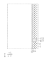
- FIG. 1 is a perspective view showing a package in which electronic components are mounted according to the first embodiment.
- FIG. 2 is a plan view of the package shown in FIG. 1 as viewed from the mounting surface side.
- FIG. 3 is a plan view of the internal structure of the package shown in FIG. 1, viewed from the non-mounting surface side.
- FIG. 4 is a cross-sectional view taken along line IV-IV shown in FIG.
- FIG. 5 is an enlarged view of region V shown in FIG. 6A is an enlarged view of a part of the top wiring shown in FIG. 5.
- FIG. 6B is an enlarged view of a portion of the pad structure shown in FIG. 5.
- FIG. FIG. 7 is a graph showing the relationship between the thickness of the wiring electrode and the stress.
- FIG. 8 is a graph showing the relationship between the thickness of the first metal film and stress.
- FIG. 9 is a graph showing the relationship between the overlap width of the base resin film and the stress.
- FIG. 10 is a graph showing the relationship between the thickness of the underlying resin film and the stress.
- 11A is a cross-sectional view showing an example of a method of manufacturing the package shown in FIG. 1.
- FIG. 11B is a cross-sectional view showing a step after the step of FIG. 11A.
- FIG. 11C is a cross-sectional view showing a step after the step of FIG. 11B.
- FIG. 11D is a cross-sectional view showing a step after the step of FIG. 11C.
- FIG. 11E is a cross-sectional view showing a step after the step of FIG.
- FIG. 11F is a cross-sectional view showing a step after the step of FIG. 11E.
- FIG. 11G is a cross-sectional view showing a step after the step of FIG. 11F.
- FIG. 11H is a cross-sectional view showing a step after the step of FIG. 11G.
- FIG. 11I is a cross-sectional view showing a step after the step of FIG. 11H.
- FIG. 11J is a cross-sectional view showing a step after the step of FIG. 11I.
- FIG. 11K is a cross-sectional view showing a step after the step of FIG. 11J.
- FIG. 11L is a cross-sectional view showing a step after the step of FIG. 11K.
- FIG. 11M is a cross-sectional view showing a step after the step of FIG. 11L.
- FIG. 11N is a cross-sectional view showing a step after the step of FIG. 11M.
- FIG. 11O is a cross-sectional view showing a step after the step of FIG. 11N.
- FIG. 11P is a cross-sectional view showing a step after the step of FIG. 11O.
- FIG. 11Q is a cross-sectional view showing a step after the step of FIG. 11P.
- FIG. 11R is a cross-sectional view showing a step after the step of FIG. 11Q.
- FIG. 11S is a cross-sectional view showing a step after the step of FIG. 11R.
- FIG. 12 is a cross-sectional view corresponding to FIG.
- FIG. 13A is a cross-sectional view showing an example of a manufacturing process of the electronic component shown in FIG. 12.
- FIG. 13B is a cross-sectional view showing a step after the step of FIG. 13A.
- FIG. 13C is a cross-sectional view showing a step after the step of FIG. 13B.
- FIG. 13D is a cross-sectional view showing a step after the step of FIG. 13C.
- FIG. 13E is a cross-sectional view showing a step after the step of FIG. 13D.
- FIG. 13F is a cross-sectional view showing a step after the step of FIG. 13E.
- FIG. 13G is a cross-sectional view showing a step after the step of FIG. 13F.
- FIG. 14 is a cross-sectional view corresponding to FIG. 4 and showing a package in which an electronic component according to the third embodiment is mounted.
- FIG. 15 is an enlarged view of region XV shown in FIG.
- FIG. 1 is a perspective view showing a package 2A mounted with an electronic component 1A according to the first embodiment.
- FIG. 2 is a plan view of the package 2A shown in FIG. 1 as viewed from the mounting surface 4 side.
- FIG. 3 is a plan view of the internal structure of the package 2A shown in FIG. 1 as viewed from the non-mounting surface 5 side.
- FIG. 4 is a cross-sectional view taken along line IV-IV shown in FIG.
- FIG. 5 is an enlarged view of region V shown in FIG.
- FIG. 6A is an enlarged view of a portion of the top wiring 25 shown in FIG.
- FIG. 6B is an enlarged view of a portion of the pad structure 65 shown in FIG. Hatching is omitted in FIGS. 6A and 6B for clarity.
- the package 2A is of the QFN (Quad Flat Non-leaded) type in this embodiment.
- the package 2A includes a hexahedral (rectangular parallelepiped in this embodiment) package body 3 .
- the package body 3 has a mounting surface 4 on one side, a non-mounting surface 5 on the other side, and first to fourth side walls 6A to 6D connecting the mounting surface 4 and the non-mounting surface 5, respectively.
- the mounting surface 4 and the non-mounting surface 5 are each formed in a quadrilateral shape when viewed from the normal direction Z (hereinafter simply referred to as "plan view").
- the first to fourth side walls 6A to 6D extend vertically along the normal direction Z.
- the first side wall 6A and the second side wall 6B extend in the first direction X along the mounting surface 4 and face the second direction Y intersecting (specifically, perpendicular to) the first direction X.
- the third side wall 6C and the fourth side wall 6D extend in the second direction Y and face the first direction X.
- the package body 3 includes a mold resin 7.
- Mold resin 7 includes a matrix resin and a plurality of fillers.
- the matrix resin may contain a thermosetting resin (eg, epoxy resin).
- the matrix resin may be colored with a coloring material such as carbon black. That is, the mold resin 7 may be an opaque resin.
- the multiple fillers are each made of spherical objects made of ceramics, oxides, insulators, etc.
- the plurality of fillers in this form, are each composed of silicon oxide particles (silica particles).
- Mold resin 7 preferably contains a plurality of fillers with different particle sizes.
- the package 2A includes a conductor plate 8 arranged inside the package body 3 .
- the conductor plate 8 may be called a "lead frame".
- the conductor plate 8 in this embodiment includes a die pad portion 9 , at least one (in this embodiment, a plurality of) lead portions 10 , and at least one (in this embodiment, a plurality of) finger portions 11 .
- the number of lead portions 10 is arbitrary.
- the presence or absence of finger portions 11 is optional, and a conductor plate 8 without finger portions 11 may be employed.
- the die pad portion 9 is arranged in the central portion of the package body 3 so as to be exposed from the mounting surface 4 .
- the die pad portion 9 is formed in a polygonal shape (specifically, a rectangular shape) having four sides parallel to the first to fourth side walls 6A to 6D in plan view.
- the planar shape of the die pad portion 9 is arbitrary.
- the die pad portion 9 has a protruding portion 9a protruding toward the first to fourth side walls 6A to 6D at the peripheral edge portion on the non-mounting surface 5 side.
- a plurality of lead portions 10 are arranged on the peripheral portion of the package body 3 with a gap from the die pad portion 9 so as to be exposed from the mounting surface 4 .
- the plurality of lead portions 10 need only be arranged along at least one of the first to fourth side walls 6A to 6D.
- a plurality (seven in this embodiment) of lead portions 10 are arranged along each of the first to fourth sidewalls 6A to 6D and are exposed from the corresponding first to fourth sidewalls 6A to 6D, respectively. ing.
- the plurality of lead portions 10 are each formed in a strip shape extending in a direction perpendicular to the corresponding first to fourth side walls 6A to 6D in plan view.
- the planar shape of the plurality of lead portions 10 is arbitrary.
- the plurality of lead portions 10 has projecting portions 10a projecting toward the die pad portion 9 (projecting portion 9a) at peripheral edge portions on the non-mounting surface 5 side.
- the plurality of finger portions 11 are drawn out from the die pad portion 9 toward the peripheral edges (first to fourth side walls 6A to 6D) of the package body 3 in plan view. That is, the finger portions 11 are fixed to the same potential as the die pad portion 9 . In this embodiment, the plurality of finger portions 11 are pulled out from the four corners of the die pad portion 9 toward the four corners of the package body 3 in plan view, and are exposed from the four corners of the package body 3 .
- the package 2A includes an electronic component 1A arranged inside the package body 3 so as to be electrically connected to the conductor plate 8.
- the electronic component 1A is arranged in a region on the non-mounting surface 5 side with respect to the conductor plate 8 so as not to be exposed from the package body 3 . That is, the entire outer surface of the electronic component 1A is covered with the mold resin 7. As shown in FIG.
- the electronic component 1A is mechanically and electrically connected to the conductor plate 8 by a flip chip connection method in this embodiment.
- the electronic component 1A is arranged inside the package body 3 so as to overlap the entire die pad portion 9, the ends of the plurality of lead portions 10, and the plurality of finger portions 11 in plan view.
- the electronic component 1A is mechanically and electrically connected to the die pad portion 9 and the ends of the plurality of lead portions 10, and is not mechanically connected to the plurality of finger portions 11.
- FIG. A specific structure of the electronic component 1A mounted in the package 2A will be described below.
- the electronic component 1A is a semiconductor device including a semiconductor chip 13 (chip).
- Semiconductor chip 13 may include at least one of silicon and a wide bandgap semiconductor.
- a wide bandgap semiconductor is a semiconductor that has a bandgap that exceeds that of silicon.
- Gallium nitride, silicon carbide, and diamond are examples of wide bandgap semiconductors.
- the semiconductor chip 13 consists of a silicon chip in this form.
- Semiconductor chip 13 may have a laminated structure including a semiconductor substrate and an epitaxial layer.
- the semiconductor chip 13 may have a single layer structure consisting of a semiconductor substrate or an epitaxial layer.
- the semiconductor chip 13 has a first main surface 14 on one side, a second main surface 15 on the other side, and first to fourth side surfaces 16A to 16D connecting the first main surface 14 and the second main surface 15. are doing.
- the first major surface 14 may also be referred to as the "terminal surface” or the “device surface”.
- the second major surface 15 may also be referred to as a "non-terminal surface” or “non-device surface.”
- the first main surface 14 and the second main surface 15 are formed in a square shape in plan view.
- the first side surface 16A and the second side surface 16B extend in the first direction X and face the second direction Y.
- the third side surface 16C and the fourth side surface 16D extend in the second direction Y and face the first direction X.
- the semiconductor chip 13 is disposed on the side of the non-mounting surface 5 with respect to the conductor plate 8 with the first main surface 14 facing the conductor plate 8 .
- the electronic component 1A includes a plurality of device regions 17 partitioned on the first main surface 14.
- multiple device regions 17 are indicated by dashed lines.
- the number and arrangement of the plurality of device regions 17 are arbitrary.
- the plurality of device regions 17 each include functional devices formed using regions inside and outside the semiconductor chip 13 .
- the functional device may include at least one of a semiconductor switching device, a semiconductor rectifying device and a passive device.
- a functional device may include a network of combined at least two of a semiconductor switching device, a semiconductor rectifying device and a passive device.
- the semiconductor switching device may include at least one of MISFET (Metal Insulator Semiconductor Field Effect Transistor), BJT (Bipolar Junction Transistor), IGBT (Insulated Gate Bipolar Junction Transistor) and JFET (Junction Field Effect Transistor) .
- MISFET Metal Insulator Semiconductor Field Effect Transistor
- BJT Bipolar Junction Transistor
- IGBT Insulated Gate Bipolar Junction Transistor
- JFET Joint Field Effect Transistor
- the semiconductor rectifier device may include at least one of a pn junction diode, a pin junction diode, a Zener diode, a Schottky barrier diode and a fast recovery diode.
- Passive devices may include at least one of resistors, capacitors, inductors and fuses.
- the electronic component 1A includes an insulating layer 20 formed on the first main surface 14. That is, the insulating layer 20 is interposed between the conductor plate 8 and the first principal surface 14 . In this embodiment, the insulating layer 20 covers the entire area of the first main surface 14 in plan view, and continues to the peripheral edge (first to fourth side surfaces 16A to 16D) of the semiconductor chip 13 .
- the insulating layer 20 includes a plurality of interlayer insulating films 21 and top insulating films 22 (to be covered).
- the number of layers of the plurality of interlayer insulating films 21 is arbitrary. As an example, the number of layers of the interlayer insulating film 21 may be 2 or more and 25 or less.
- Each of the plurality of interlayer insulating films 21 may have a single layer structure or a laminated structure including at least one of a silicon oxide film and a silicon nitride film.
- the plurality of interlayer insulating films 21 each have a single-layer structure made of a silicon oxide film in this embodiment.
- the top insulating film 22 forms a terminal insulating film of the insulating layer 20 and covers the uppermost interlayer insulating film 21 .
- the top insulating film 22 may be called an "inorganic insulating film” or a "passivation film”.
- the top insulating film 22 may have a single layer structure including at least one of a silicon oxide film and a silicon nitride film.
- the top insulating film 22 preferably contains an insulating material different from at least the uppermost interlayer insulating film 21 .
- the top insulating film 22 has a single-layer structure made of a silicon nitride film in this embodiment.
- Top insulating film 22 has a flat surface extending along first main surface 14 .
- the top insulating film 22 preferably has a thickness at least less than the thickness of the uppermost interlayer insulating film 21 .
- the thickness of the top insulating film 22 is less than the thickness of each interlayer insulating film 21 in this embodiment.
- the electronic component 1A includes a plurality of interlayer wirings 23 arranged within the insulating layer 20 .
- a plurality of interlayer wirings 23 are wiring films arranged on an arbitrary interlayer insulating film 21 in a layer below the top insulating film 22 .
- the routing form of the plurality of interlayer wirings 23 is arbitrary.
- a plurality of interlayer wirings 23 form a multilayer wiring structure 24 (to be covered) together with a plurality of interlayer insulating films 21 .
- the plurality of interlayer wirings 23 may include at least one of an Al-based metal film and a Cu-based metal film.
- the plurality of interlayer wirings 23 are composed of at least one of a pure Al film (an Al film with a purity of 99% or higher), a pure Cu film (a Cu film with a purity of 99% or higher), an AlCu alloy film, an AlSi alloy film, and an AlSiCu alloy film. may contain one.
- the electronic component 1A includes a plurality of top wirings 25 arranged on the insulating layer 20 (specifically, the top insulating film 22).
- a plurality of top wirings 25 form terminal wirings of the multilayer wiring structure 24 respectively.
- the routing form of the plurality of top wirings 25 is arbitrary.
- the plurality of top wirings 25 may be routed in a line shape in a plan view, or may be formed in an island shape.
- the plurality of top wirings 25 may have relatively wide island portions in a plan view and relatively narrow line portions extending in a line form from the island portions.
- the plurality of top wirings 25 each have a thickness exceeding the thickness of the top insulating film 22 . It is preferable that each of the plurality of top wirings 25 has a thickness exceeding the thickness of each interlayer wiring 23 . It is preferable that the plurality of top wirings 25 have a thickness less than the thickness of some of the plurality of fillers contained in the mold resin 7 .
- a plurality of wiring layers have the same configuration except for the arrangement location and routing form. The structure of one top wiring 25 will be specifically described below.
- top wiring 25 includes a wiring barrier film 30 that selectively covers top insulating film 22 .
- the wiring barrier film 30 extends substantially flat along the top insulating film 22 .
- the wiring barrier film 30 is made of a hard metal film having a relatively small coefficient of thermal expansion.
- the thermal expansion coefficient of the wiring barrier film 30 may be 4 ⁇ m/m ⁇ K or more and 9 ⁇ m/m ⁇ K or less.
- the wiring barrier film 30 preferably includes at least one of Ti film, TiN film, Ta film, W film, Mo film, Cr film and Ru film.
- the wiring barrier film 30 preferably contains a Ti-based metal.
- the wiring barrier film 30 may have a laminated structure or a single layer structure including at least one of a Ti film and a TiN film.
- the wiring barrier film 30 may have a laminated structure including a Ti film and a TiN film laminated in this order from the top insulating film 22 side.
- the wiring barrier film 30 has a single-layer structure made of a Ti film in this embodiment.
- the wiring barrier film 30 has a first thickness T1 in the stacking direction.
- the stacking direction is the normal direction Z (same hereafter).
- the first thickness T1 may be 0.01 ⁇ m or more and 0.5 ⁇ m or less.
- the first thickness T1 is preferably 0.05 ⁇ m or more and 0.2 ⁇ m or less.
- the top wiring 25 includes wiring electrodes 31 covering the wiring barrier film 30 .
- the wiring electrode 31 forms the main body of the top wiring 25 .
- the wiring electrode 31 includes a metal film different from the wiring barrier film 30 .
- the wiring electrode 31 specifically includes a low-hardness metal film having a thermal expansion coefficient exceeding that of the wiring barrier film 30 .
- the wiring electrode 31 may include at least one of an Al-based metal film and a Cu-based metal film.
- the wiring electrode 31 is at least one of a pure Al film (an Al film with a purity of 99% or more), a pure Cu film (a Cu film with a purity of 99% or more), an AlCu alloy film, an AlSi alloy film, or an AlSiCu alloy film. may contain
- the wiring electrode 31 is preferably made of a Cu-based metal film.
- the wiring electrode 31 consists of a pure Cu film
- the thermal expansion coefficient of the wiring electrode 31 is about 16.5 ⁇ m/m ⁇ K in this form.
- the wiring electrode 31 has a second thickness T2 (T1 ⁇ T2) that exceeds the first thickness T1 of the wiring barrier film 30 in the stacking direction.
- the second thickness T2 may be 1 ⁇ m or more and 15 ⁇ m or less.
- the wiring electrode 31 covers the entire wiring barrier film 30 in cross-sectional view and plan view.
- the wiring electrode 31 has a peripheral portion projecting outside the wiring barrier film 30 so as to face the top insulating film 22 in the stacking direction.
- the wiring electrode 31 includes a wiring lower surface 32 , a wiring upper surface 33 and wiring sidewalls 34 .
- the wiring lower surface 32 extends substantially flat along the wiring barrier film 30 .
- the wiring upper surface 33 extends substantially flat along the wiring barrier film 30 .
- the wiring sidewall 34 is located on the top insulating film 22 and extends substantially vertically in the stacking direction. "Substantially vertical” also includes a form extending in the stacking direction while curving (meandering).
- the wiring sidewall 34 is positioned outside the wiring barrier film 30 and faces the top insulating film 22 without the wiring barrier film 30 interposed therebetween in the stacking direction.
- the wiring sidewall 34 has a wiring upper end portion 35 on the wiring upper surface 33 side and a wiring lower end portion 36 on the top insulating film 22 side.
- the wiring sidewall 34 has a wiring recess portion 37 recessed inwardly at the wiring lower end portion 36 .
- the wiring recess portion 37 forms an uneven portion (wiring uneven portion) at the wiring lower end portion 36 .
- the wiring recess portion 37 may be recessed inwardly from the wiring upper end portion 35 .
- the wiring recess portion 37 may be recessed in a curved shape.
- the wiring recess portion 37 exposes the peripheral portion of the wiring barrier film 30 .
- the wiring recess portion 37 has an upper end located outside the peripheral edge of the wiring barrier film 30 and a lower end located inside the peripheral edge of the wiring barrier film 30 .
- the wiring recess portion 37 also exposes the top insulating film 22 in this embodiment.
- the wiring recess portion 37 is formed with a space from the intermediate portion of the wiring side wall 34 toward the top insulating film 22 side.
- the wiring recess portion 37 has a first longitudinal width W1 (T1 ⁇ W1) that exceeds the first thickness T1 of the wiring barrier film 30 in the stacking direction.
- the first vertical width W1 may be 0.01 ⁇ m or more and 1 ⁇ m or less.
- the first vertical width W1 is preferably 0.5 ⁇ m or less.
- the wiring recess portion 37 has a first lateral width W2 (T1 ⁇ W2) exceeding the first thickness T1 in the directions perpendicular to the stacking direction (the first direction X and the second direction Y).
- the first width W2 may be 0.01 ⁇ m or more and 1 ⁇ m or less.
- the first width W2 is preferably 0.5 ⁇ m or less.
- the wiring electrode 31 has a wiring upper end corner portion 38 formed in a round shape.
- the wiring upper end corner portion 38 is a corner portion that connects the wiring upper surface 33 and the wiring side wall 34 (the wiring upper end portion 35). That is, the wiring upper end corner portion 38 connects the wiring upper surface 33 and the wiring side wall 34 in an arc shape (curved shape). That is, the wiring upper end corner portion 38 is inclined obliquely downward in an arc shape from the wiring upper surface 33 toward the wiring side wall 34 at the peripheral edge portion of the wiring upper surface 33 .
- the center of curvature of the arc is positioned either inside the wiring electrode 31 or inside the interlayer insulating film 21 (top insulating film 22).
- the wiring top corner portion 38 includes a portion facing the wiring barrier film 30 in the stacking direction and a portion not facing the wiring barrier film 30 .
- the width of the portion of the wiring top corner portion 38 that does not face the wiring barrier film 30 is less than the width of the portion of the wiring top corner portion 38 that faces the wiring barrier film 30 .
- the wiring upper end corner portion 38 has a round start point P1 and a round end point P2.
- the round starting point P1 is positioned on the wiring upper surface 33 side.
- the round end point P2 is located on the wiring side wall 34 side.
- the wiring upper end corner portion 38 has a round width WR in the direction orthogonal to the stacking direction.
- the round width WR is the distance between the round start point P1 and the round end point P2 in the direction orthogonal to the stacking direction.
- the round width WR preferably exceeds the first lateral width W2 of the wiring recess portion 37 (W2 ⁇ WR). Also, the round width WR preferably exceeds the first vertical width W1 of the wiring recess portion 37 (W1 ⁇ WR).
- the round width WR is preferably less than the second thickness T2 of the wiring electrode 31 (WR ⁇ T2).
- the round width WR may be 1 ⁇ m or more and 20 ⁇ m or less.
- a first virtual line L1 and a second virtual line L2 are set in the vicinity of the upper end corner portion 38 of the wiring.
- the first virtual line L ⁇ b>1 is a virtual line extending along the wiring upper surface 33 .
- the second virtual line L2 is a virtual line that connects the round start point P1 and the round end point P2.
- the wiring upper end corner portion 38 is such that the angle ⁇ between the first virtual line L1 and the second virtual line L2 exceeds 0° and is 45° or less. It is preferably formed to belong to the range. In this embodiment, the wiring upper end corner portion 38 is formed so that the angle ⁇ falls within the range of 10° or more and 30° or less.
- the top wiring 25 includes wiring cover electrodes 41 that cover the wiring electrodes 31 .
- the wiring cover electrode 41 includes a conductor different from the wiring electrode 31 and covers the entire wiring electrode 31 in a film form.
- the wiring cover electrode 41 has a third thickness T3 (T3 ⁇ T2) less than the second thickness T2 of the wiring electrode 31 in the stacking direction.
- the third thickness T3 may be 0.55 ⁇ m or more and 11 ⁇ m or less.
- the third thickness T3 is preferably 1.1 ⁇ m or more and 2.5 ⁇ m or less.
- the third thickness T3 preferably has a thickness less than the thickness of some of the multiple fillers contained in the mold resin 7 .
- the wiring cover electrode 41 has a first lower surface 42 , a first upper surface 43 , and a first peripheral wall 44 connecting the first lower surface 42 and the first upper surface 43 .
- the first bottom surface 42 extends along the wiring top surface 33
- the first top surface 43 extends along the wiring top surface 33 .
- the first peripheral wall 44 is a side wall of the wiring cover electrode 41 and extends substantially vertically along the stacking direction. "Substantially vertical" also includes a form extending in the stacking direction while curving (meandering).
- the wiring cover electrode 41 includes a round portion 45 that covers the upper corner portion 38 of the wiring in a film shape so as to curve along the upper corner portion 38 of the wiring. That is, the round portion 45 is formed in a film shape so that the first lower surface 42 and the first upper surface 43 are curved along the wiring upper end corner portion 38 . Further, the round portion 45 is formed so as to incline downward in an arc shape from the wiring upper surface 33 side toward the wiring side wall 34 side. The round portion 45 covers the entire area between the round start point P1 and the round end point P2 at the upper end corner portion 38 of the wiring. The round portion 45 forms a round end portion P2 at the connection portion with the wiring side wall 34 .
- the wiring cover electrode 41 further has a first extending portion 46 extending to a region outside the wiring cover electrode 41 (wiring upper end corner portion 38).
- the first extending portion 46 forms the peripheral portion of the wiring cover electrode 41 and is composed of the first lower surface 42 , the first upper surface 43 and the first peripheral wall 44 .
- the first extending portion 46 is formed in an arc shape continuously extending from the round portion 45 and has a portion located closer to the top insulating film 22 than the wiring upper surface 33 .
- the first extension 46 faces the top insulating film 22 in the stacking direction, and faces the wiring electrode 31 (wiring side wall 34) in the direction perpendicular to the stacking direction.
- the first extended portion 46 has a lower end located between the wiring upper surface 33 and the top insulating film 22 .
- the lower end portion of the first extending portion 46 is formed by the connecting portion of the first lower surface 42 extending in an arc shape and the first peripheral wall 44 extending substantially vertically, and has a sharp shape forming an acute angle in a cross-sectional view.
- the first extending portion 46 has a first extending width W3 in the direction perpendicular to the stacking direction.
- the first extension width W3 preferably exceeds the first vertical width W1 of the wiring recess portion 37 (W1 ⁇ W3).
- the first extension width W3 preferably exceeds the first lateral width W2 of the wiring recess portion 37 (W2 ⁇ W3).
- the first extending width W3 is preferably less than the round width WR (W3 ⁇ WR).
- the first extension width W3 is preferably equal to or less than the third thickness T3 of the wiring cover electrode 41 (W3 ⁇ T3). Of course, the first extension width W3 may exceed the third thickness T3 of the wiring cover electrode 41 (T3 ⁇ W3).
- the wiring cover electrode 41 has a laminated structure in which a plurality of metal films are laminated.
- the wiring cover electrode 41 includes a first metal film 47 and a second metal film 48 laminated in this order from the wiring electrode 31 side.
- the first metal film 47 covers the entire wiring upper surface 33 in a film shape, and forms part of the first lower surface 42 and the first peripheral wall 44 of the wiring cover electrode 41 .
- the first metal film 47 includes a metal film with hardness higher than that of the wiring electrode 31 .
- the first metal film 47 preferably contains a Ni-based metal film.
- the first metal film 47 includes a pure Ni film (a Ni film with a purity of 99% or higher) in this embodiment.
- the first metal film 47 has a fourth thickness T4.
- the fourth thickness T4 may be 0.5 ⁇ m or more and 6 ⁇ m or less.
- the second metal film 48 covers the entire area of the second metal film 48 in a film form, and forms part of the first upper surface 43 and the first peripheral wall 44 of the wiring cover electrode 41 .
- the second metal film 48 preferably contains a Pd-based metal film.
- the second metal film 48 includes a pure Pd film (a Pd film with a purity of 99% or higher) in this embodiment.
- the second metal film 48 has a fifth thickness T5 less than the fourth thickness T4 of the first metal film 47 (T5 ⁇ T4).
- the fifth thickness T5 may be 0.05 ⁇ m or more and 1 ⁇ m or less.
- the fifth thickness T5 is preferably 0.1 ⁇ m or more and 0.5 ⁇ m or less.
- the total value of the fourth thickness T4 and the fifth thickness T5 is the third thickness T3.
- electronic component 1A includes a plurality of via electrodes 50 arranged in insulating layer 20.
- the plurality of via electrodes 50 includes a plurality of first via electrodes 51 arranged within the interlayer insulating film 21 and a plurality of second via electrodes 52 arranged within the top insulating film 22 .
- a plurality of first via electrodes 51 penetrate the corresponding interlayer insulating films 21 so as to electrically connect a plurality of arbitrary interlayer wirings 23 facing each other in the stacking direction.
- a plurality of second via electrodes 52 respectively penetrate the top insulating film 22 and the uppermost interlayer insulating film 21 so as to electrically connect arbitrary interlayer wirings 23 and arbitrary top wirings 25 facing each other in the stacking direction. .
- a plurality of via electrodes 50 are embedded in via holes 53 formed in the insulating layer 20 respectively.
- a plurality of via electrodes 50 each have a laminated structure including a via barrier film 54 and a via body 55 .
- the via barrier film 54 coats the inner wall of the via hole 53 in a film form.
- the via barrier film 54 may contain a Ti-based metal film.
- the via body 55 is embedded in the via hole 53 with the via barrier film 54 interposed therebetween. Via body 55 may include tungsten.
- electronic component 1A includes base resin film 60 (organic film) formed on insulating layer 20. As shown in FIG. That is, the underlying resin film 60 is interposed between the conductor plate 8 and the multilayer wiring structure 24 .
- the underlying resin film 60 has an elastic modulus lower than that of the top insulating film 22 and is relatively soft.
- the underlying resin film 60 is made of a resin material different from the mold resin 7 described above.
- the underlying resin film 60 specifically contains a photosensitive resin (that is, a transparent resin).
- Base resin film 60 may include at least one of an epoxy resin film, a polyimide resin film, a polyamide resin film, a polybenzoxazole resin film, and a phenol resin film.
- the underlying resin film 60 has a single-layer structure made of a phenolic resin film in this embodiment.
- the base resin film 60 is spaced inwardly from the peripheral edge (first to fourth side surfaces 16A to 16D) of the insulating layer 20 in plan view, and exposes the peripheral edge of the insulating layer 20. As shown in FIG.
- the base resin film 60 covers the wiring sidewalls 34 of the wiring electrodes 31 in the regions between the plurality of top wirings 25 on the insulating layer 20 .
- the underlying resin film 60 fills the wiring recess portion 37 at the wiring lower end portion 36 of the wiring side wall 34 .
- the underlying resin film 60 is in contact with the top insulating film 22 , the wiring barrier film 30 and the wiring electrode 31 within the wiring recess portion 37 .
- the base resin film 60 fills the gap between the wiring side wall 34 and the first extending portion 46 of the wiring cover electrode 41 at the wiring upper end portion 35 of the wiring side wall 34 . That is, the underlying resin film 60 is in contact with the wiring sidewall 34 of the wiring electrode 31 and the first lower surface 42 of the wiring cover electrode 41 on the wiring upper end portion 35 side.
- the underlying resin film 60 includes an overlapping portion 61 covering the first upper surface 43 of the wiring cover electrode 41 .
- the overlap portion 61 extends inwardly of the first upper surface 43 from the first peripheral wall 44 .
- the overlapping portion 61 defines a pad opening 62 that partially exposes the wiring cover electrode 41 in the inner portion of the wiring cover electrode 41 .
- the overlap portion 61 covers the wiring upper end corner portion 38 of the wiring electrode 31 with the wiring cover electrode 41 interposed therebetween.
- the overlap portion 61 preferably covers the entire round portion 45 of the wiring cover electrode 41 .
- the overlap portion 61 preferably covers the entire region between the round start portion P1 and the round end portion P2 of the wiring electrode 31 with the wiring cover electrode 41 interposed therebetween.
- the overlap portion 61 has an overlap width WO (WR ⁇ WO) equal to or larger than the round width WR in the direction orthogonal to the stacking direction.
- the overlap width WO may be 1 ⁇ m or more and 40 ⁇ m or less.
- the overlap width WO may exceed the second thickness T2 of the wiring electrode 31 (T2 ⁇ WO), or may be equal to or less than the second thickness T2 (WO ⁇ T2).
- the overlap portion 61 has a sixth thickness T6 in the stacking direction.
- the sixth thickness T6 may be 1 ⁇ m or more and 40 ⁇ m or less.
- the sixth thickness T6 may exceed the third thickness T3 of the wiring cover electrode 41 (T3 ⁇ T6).
- the sixth thickness T6 may exceed the round width WR (WR ⁇ T6).
- the sixth thickness T6 may exceed the second thickness T2 (T2 ⁇ T6) or may be equal to or less than the second thickness T2 (T6 ⁇ T2).
- the sixth thickness T6 preferably has a thickness less than the thickness of some of the multiple fillers contained in the mold resin 7 .
- electronic component 1A has a plurality of pad structures 65 respectively arranged on corresponding top wirings 25 so as to be electrically connected to corresponding top wirings 25.
- a plurality of pad structures 65 are terminal electrodes interposed between the conductor plate 8 and the top wiring 25 to electrically connect the conductor plate 8 and the top wiring 25 .
- a specific structure of one pad structure 65 will be described below.
- the pad structure 65 includes a pad barrier film 70 selectively covering the top wiring 25 .
- the pad barrier film 70 covers the first upper surface 43 of the wiring cover electrode 41 and the overlapping portion 61 of the base resin film 60 in a film form. A portion of the pad barrier film 70 covering the overlap portion 61 is located above a portion of the pad barrier film 70 covering the first upper surface 43 .
- the pad barrier film 70 is made of a hard metal film having a relatively small coefficient of thermal expansion.
- Pad barrier film 70 includes at least one of Ti film, TiN film, Ta film, W film, Mo film, Cr film and Ru film.
- the coefficient of thermal expansion of the pad barrier film 70 may be 4 ⁇ m/m ⁇ K or more and 9 ⁇ m/m ⁇ K or less.
- the pad barrier film 70 preferably contains a Ti-based metal.
- the pad barrier film 70 may have a laminated structure or a single layer structure including at least one of a Ti film and a TiN film.
- the pad barrier film 70 may have a laminated structure including a Ti film and a TiN film laminated in this order from the top wiring 25 side.
- the pad barrier film 70 has a single layer structure made of a Ti film in this embodiment.
- the pad barrier film 70 has a seventh thickness T7 in the stacking direction.
- the seventh thickness T7 may be 0.01 ⁇ m or more and 0.5 ⁇ m or less.
- the seventh thickness T7 is preferably 0.05 ⁇ m or more and 0.2 ⁇ m or less.
- the pad barrier film 70 may have the same material and/or the same thickness as the wiring barrier film 30 .
- the pad structure 65 includes a pad electrode 71 covering the pad barrier film 70 .
- a pad electrode may be referred to as a "terminal electrode”.
- the pad electrode 71 forms the main body of the pad structure 65 and has a columnar shape standing along the stacking direction in a cross-sectional view.
- Pad electrode 71 includes a metal film different from pad barrier film 70 .
- Pad electrode 71 specifically includes a low-hardness metal film having a thermal expansion coefficient exceeding that of pad barrier film 70 .
- the pad electrode 71 may include at least one of an Al-based metal film and a Cu-based metal film.
- the pad electrode 71 is at least one of a pure Al film (an Al film with a purity of 99% or more), a pure Cu film (a Cu film with a purity of 99% or more), an AlCu alloy film, an AlSi alloy film, and an AlSiCu alloy film. may contain
- the pad electrode 71 is preferably made of a Cu-based metal film.
- the pad electrode 71 consists of a pure Cu film in this form.
- the coefficient of thermal expansion of the pad electrode 71 is approximately 16.5 ⁇ m/m ⁇ K in this embodiment.
- the pad electrode 71 has an eighth thickness T8 (T7 ⁇ T8) that exceeds the seventh thickness T7 of the pad barrier film 70 in the stacking direction.
- the eighth thickness T8 is the thickness of the pad electrode 71 with the top wiring 25 (wiring cover electrode 41) as a reference (zero point).
- the eighth thickness T8 exceeds the second thickness T2 of the wiring electrode 31 (T2 ⁇ T8).
- the eighth thickness T8 is preferably less than the thickness of the conductor plate 8.
- the eighth thickness T8 preferably exceeds the sixth thickness T6 of the underlying resin film 60 (overlapping portion 61) (T6 ⁇ T8).
- the eighth thickness T8 may be 10 ⁇ m or more and 100 ⁇ m or less.
- the eighth thickness T8 is preferably 20 ⁇ m or more and 60 ⁇ m or less.
- the eighth thickness T8 preferably has a thickness exceeding the thickness of the plurality of fillers contained in the molding resin 7. As shown in FIG.
- the pad electrode 71 covers the overlapping portion 61 of the base resin film 60 with a space inward from the wiring upper end corner portion 38 of the wiring electrode 31 in plan view. That is, the pad electrode 71 is spaced inwardly from the round portion 45 of the wiring cover electrode 41 and does not face the round portion 45 with the underlying resin film 60 (overlap portion 61) interposed therebetween.
- the pad electrode 71 enters the pad opening 62 from above the underlying resin film 60 (overlapping portion 61 ) and is connected to the wiring cover electrode 41 via the pad barrier film 70 within the pad opening 62 .
- the pad electrode 71 covers the entire pad barrier film 70 in cross-sectional view and plan view.
- the pad electrode 71 has a peripheral portion that protrudes outside the pad barrier film 70 and faces the underlying resin film 60 in the stacking direction.
- the pad electrode 71 includes a pad lower surface 72 , a pad upper surface 73 and pad sidewalls 74 .
- Pad lower surface 72 extends along first upper surface 43 of wiring cover electrode 41 and overlapping portion 61 of underlying resin film 60 .
- a portion of the pad lower surface 72 that covers the overlap portion 61 is located above a portion of the pad lower surface 72 that covers the first upper surface 43 .
- the pad upper surface 73 extends along the overlap portion 61 between the first upper surface 43 of the wiring cover electrode 41 and the underlying resin film 60 .
- a portion of the pad upper surface 73 that covers the first upper surface 43 is recessed toward the wiring cover electrode 41 . That is, the portion of the pad upper surface 73 that covers the overlap portion 61 is located above the portion of the pad upper surface 73 that covers the first upper surface 43 .
- the pad side wall 74 is located on the underlying resin film 60 and extends substantially vertically along the normal direction Z. As shown in FIG. "Substantially vertical" also includes a form extending in the stacking direction while curving (meandering). The pad sidewall 74 is positioned outside the pad barrier film 70 and faces the base resin film 60 in the stacking direction without the pad barrier film 70 interposed therebetween.
- the pad side wall 74 has a pad upper end portion 75 on the pad upper surface 73 side and a pad lower end portion 76 on the underlying resin film 60 side.
- the pad side wall 74 has a pad recess portion 77 recessed inwardly from the pad upper end portion 75 at the pad lower end portion 76 .
- the pad recess portion 77 forms an uneven portion (pad uneven portion) at the pad lower end portion 76 .
- the pad recess portion 77 may be recessed inwardly from the pad upper end portion 75 .
- the pad recess portion 77 may be recessed in a curved shape.
- the pad recess portion 77 exposes the peripheral portion of the pad barrier film 70 .
- the pad recess portion 77 has an upper end located outside the peripheral edge of the pad barrier film 70 and a lower end located inside the peripheral edge of the pad barrier film 70 .
- the pad recess portion 77 also exposes the base resin film 60 .
- the pad recess portion 77 is formed with a space from the intermediate portion of the pad side wall 74 toward the top wiring 25 side.
- the pad recess portion 77 has a second longitudinal width W4 (T7 ⁇ W4) that exceeds the seventh thickness T7 of the pad barrier film 70 in the stacking direction.
- the second vertical width W4 may be 0.01 ⁇ m or more and 1 ⁇ m or less.
- the second vertical width W4 is preferably 0.5 ⁇ m or less.
- the pad recess portion 77 has a second lateral width W5 (T7 ⁇ W5) that exceeds the seventh thickness T7 of the pad barrier film 70 in the direction orthogonal to the stacking direction.
- the second width W5 may be 0.01 ⁇ m or more and 1 ⁇ m or less.
- the second width W5 is preferably 0.5 ⁇ m or less.
- the pad electrode 71 has an angular pad upper corner 78 unlike the wiring upper corner 38 of the wiring electrode 31 .
- Pad upper end corner portion 78 is a corner portion connecting pad upper surface 73 and pad side wall 74 (pad upper end portion 75).
- the pad upper end corner portion 78 may have a sharp shape protruding upward at an acute angle in a cross-sectional view due to the depression.
- the wiring top corner portion 38 faces the base resin film 60 in the stacking direction without the pad barrier film 70 interposed therebetween.
- the pad electrode 71 includes a pad cover electrode 81 covering the pad electrode 71 .
- the pad cover electrode 81 contains a conductor different from the pad electrode 71 and covers the entire area of the pad electrode 71 in a film form.
- the pad cover electrode 81 has a ninth thickness T9 (T9 ⁇ T8) that is less than the eighth thickness T8 of the pad electrode 71 in the stacking direction.
- the ninth thickness T9 may be 0.5 ⁇ m or more and 6 ⁇ m or less.
- the ninth thickness T9 is preferably 1 ⁇ m or more and 5 ⁇ m or less.
- the ninth thickness T9 preferably has a thickness less than the thickness of some of the plurality of fillers contained in the mold resin 7 .
- the pad cover electrode 81 has a second lower surface 82 , a second upper surface 83 , and a second peripheral wall 84 connecting the second lower surface 82 and the second upper surface 83 .
- the second bottom surface 82 extends along the pad top surface 73 and the second top surface 83 extends along the pad top surface 73 .
- the second peripheral wall 84 is a side wall of the pad cover electrode 81 and extends substantially vertically along the stacking direction. "Substantially vertical" also includes a form extending in the stacking direction while curving (meandering).
- the pad cover electrode 81 has a second extending portion 86 extending to a region outside the pad cover electrode 81 (pad top corner portion 78).
- the second extended portion 86 forms the peripheral portion of the pad cover electrode 81 and is composed of the second lower surface 82 , the second upper surface 83 and the second peripheral wall 84 .
- the second extending portion 86 faces the top wiring 25 in the stacking direction.
- the angle formed by the second lower surface 82 of the pad cover electrode 81 and the second peripheral wall 84 exceeds the angle formed by the first lower surface 42 and the first peripheral wall 44 of the wiring cover electrode 41 .
- the second extending portion 86 has a second extending width W6 in the direction perpendicular to the stacking direction.
- the second extension width W6 preferably exceeds the second longitudinal width W4 of the pad recess portion 77 (W4 ⁇ W6).
- the second extension width W6 preferably exceeds the second lateral width W5 of the pad recess portion 77 (W5 ⁇ W6).
- the second extension width W6 is preferably equal to or less than the ninth thickness T9 of the pad cover electrode 81 (W6 ⁇ T9). Of course, the second extension width W6 may exceed the ninth thickness T9 of the pad cover electrode 81 (T9 ⁇ W6).
- the pad cover electrode 81 has a single layer structure consisting of a single third metal film 87 in this form.
- the third metal film 87 covers the entire area of the pad upper surface 73 in a film form, and forms the second lower surface 82 , the second upper surface 83 and the second peripheral wall 84 of the wiring cover electrode 41 .
- the third metal film 87 includes a metal film with hardness higher than that of the pad electrode 71 .
- the third metal film 87 preferably contains a Ni-based metal film.
- the third metal film 87 includes a pure Ni film (a Ni film with a purity of 99% or higher) in this embodiment.
- the pad structure 65 further includes a plurality of low melting point metals 90 each arranged on the corresponding pad electrode 71 so as to be electrically connected to the corresponding pad electrode 71 .
- Low melting point metal 90 is interposed between conductor plate 8 and pad electrode 71 to mechanically and electrically connect conductor plate 8 and pad electrode 71 .
- the low melting point metal 90 is solder in this form.
- the low melting point metal 90 is preferably lead-free solder.
- the low melting point metal 90 is made of solder containing at least one of Sn and Ag in this form. The structure of one low melting point metal 90 is described below.
- the low melting point metal 90 is arranged on the pad upper surface 73 so as to expose the pad sidewalls 74 of the pad electrode 71 .
- the low melting point metal 90 fills the depression of the pad upper surface 73 above the pad cover electrode 81 .
- the low melting point metal 90 covers the entire area of the pad upper surface 73 in this form.
- the low melting point metal 90 covers the second extended portion 86 of the pad cover electrode 81 so as to expose the second peripheral wall 84 of the pad cover electrode 81 .
- the low melting point metal 90 may partially cover the second peripheral wall 84 so as to partially expose the second peripheral wall 84 .
- the low-melting-point metal 90 faces the underlying resin film 60 with the second extended portion 86 interposed therebetween.
- the low-melting-point metal 90 has a bulging portion 91 projecting outside the second extended portion 86 .
- the bulging portion 91 protrudes in an arc shape with the second extending portion 86 as a starting point.
- the bulging portion 91 faces the underlying resin film 60 without the second extending portion 86 interposed therebetween.
- the low melting point metal 90 has a tenth thickness T10 (T9 ⁇ T10) that exceeds the ninth thickness T9 in the stacking direction.
- a tenth thickness T10 is the maximum thickness of the low melting point metal 90 .
- the tenth thickness T10 preferably exceeds the second thickness T2 of the wiring electrode 31 (T2 ⁇ T10).
- the tenth thickness T10 may be equal to or less than the eighth thickness T8 (T10 ⁇ T8) of the pad electrode 71, or may exceed the eighth thickness T8 (T8 ⁇ T10).
- the tenth thickness T ⁇ b>10 is preferably less than the thickness of the conductor plate 8 .
- the tenth thickness T10 preferably has a thickness less than the thickness of some of the plurality of fillers contained in the mold resin 7 .
- electronic component 1A includes top resin 95 that coats bottom resin film 60 .
- the overlying resin 95 is made of a resin material different from that of the underlying resin film 60 .
- the overlying resin 95 has an elastic modulus higher than that of the underlying resin film 60 and a hardness higher than that of the underlying resin film 60 .
- the overlying resin 95 consists of a part of the above-mentioned mold resin 7 in this form.
- the top resin 95 is interposed between the conductor plate 8 and the base resin film 60 and covers the conductor plate 8 , the base resin film 60 , the plurality of pad electrodes 71 and the plurality of low melting point metals 90 . Further, the top resin 95 covers the peripheral portion of the insulating layer 20 exposed from the base resin film 60 .
- the overlying resin 95 covers the pad sidewalls 74 of the pad electrodes 71 in regions between the plurality of pad electrodes 71 on the underlying resin film 60 .
- the overlying resin 95 has a portion covering the top insulating film 22 with the underlying resin film 60 interposed therebetween.
- the overlying resin 95 has a portion covering the wiring upper end corner portion 38 of the wiring electrode 31 with the underlying resin film 60 interposed therebetween.
- the overlying resin 95 fills the pad recess portion 77 at the pad lower end portion 76 of the pad side wall 74 .
- the overlying resin 95 is in contact with the underlying resin film 60 , the pad barrier film 70 and the pad electrode 71 in the pad recess portion 77 .
- the upper base resin 95 is in contact with the pad side wall 74 and the second extending portion 86 (second lower surface 82 ) of the pad cover electrode 81 at the pad upper end portion 75 of the pad side wall 74 .
- the top resin 95 covers the second peripheral wall 84 and the low melting point metal 90 of the pad electrode 71 and does not cover the second upper surface 83 of the pad electrode 71 .
- the electronic component 1A includes the semiconductor chip 13, the multilayer wiring structure 24 (insulating layer 20), the pad structure 65 (a plurality of pad electrodes 71) and a plurality of low melting point metals 90.
- the electronic component 1A is arranged in the package body 3 with the pad structure 65 facing the conductor plate 8.
- a plurality of pad electrodes 71 are joined to corresponding locations (die pad portion 9 or lead portion 10 ) of conductor plate 8 via corresponding low-melting-point metals 90 .
- the electric signal from the conductor plate 8 is applied to the electronic component 1A, and the electric signal from the electronic component 1A is applied to the conductor plate 8.
- FIG. 7 is a graph showing the relationship between the second thickness T2 of the wiring electrode 31 and stress.
- the vertical axis indicates the stress [Mpa]
- the horizontal axis indicates the second thickness T2 [ ⁇ m].
- the graph of FIG. 7 shows the stress when the second thickness T2 is changed from 4 ⁇ m to 14 ⁇ m.
- the stress varies depending on the second thickness T2. Specifically, the stress increases with increasing second thickness T2. Therefore, the smaller the second thickness T2, the better. However, reducing the second thickness T2 increases the resistance value. Therefore, the second thickness T2 is preferably 6 ⁇ m or more and 12 ⁇ m or less. It is particularly preferable that the second thickness T2 is 10 ⁇ m or less. In this case, stress caused by the second thickness T2 can be suppressed to 300 Mpa or less while suppressing an increase in resistance value.
- FIG. 8 is a graph showing the relationship between the fourth thickness T4 of the first metal film 47 and stress.
- the vertical axis indicates the stress [Mpa]
- the horizontal axis indicates the fourth thickness T4 [ ⁇ m].
- the graph of FIG. 8 shows the stress when the fourth thickness T4 is changed from 1 ⁇ m to 5 ⁇ m.
- the stress varies depending on the fourth thickness T4. Specifically, the stress increases as the fourth thickness T4 increases. Therefore, it is preferable that the fourth thickness T4 be as small as possible. However, if the fourth thickness T4 is reduced, the film formability of the first metal film 47 (especially the first extending portion 46) with respect to the wiring electrode 31 is lowered. Therefore, the fourth thickness T4 is preferably 1 ⁇ m or more and 3 ⁇ m or less. In this case, the stress caused by the fourth thickness T4 can be suppressed to 300 Mpa or less while suppressing the deterioration of the film formation properties.
- FIG. 9 is a graph showing the relationship between the overlap width WO of the base resin film 60 and stress.
- the vertical axis indicates the stress [Mpa] and the horizontal axis indicates the overlap width WO [ ⁇ m].
- the graph of FIG. 9 shows the stress when the overlap width WO is varied from 1 ⁇ m to 30 ⁇ m.
- the stress varies depending on the overlap width WO.
- the stress specifically decreases with increasing overlap width WO. Therefore, it is preferable that the overlap width WO is large. Also, by increasing the overlap width WO, the top wiring 25 can be properly protected.
- the overlap width WO is preferably 5 ⁇ m or more. It is particularly preferable that the overlap width WO is 10 ⁇ m or more.
- the stress caused by the overlap width WO can be suppressed to 300 Mpa or less while appropriately protecting the top wiring 25 .
- the overlap width WO is increased too much, the area of the exposed portion (pad opening 62) of the top wiring 25 is reduced.
- the upper limit of the overlap width WO may be 20 ⁇ m or less.
- FIG. 10 is a graph showing the relationship between the sixth thickness T6 of the base resin film 60 and stress.
- the vertical axis indicates the stress [Mpa]
- the horizontal axis indicates the sixth thickness T6 [ ⁇ m].
- the graph of FIG. 10 shows the stress when the sixth thickness T6 is changed from 1 ⁇ m to 30 ⁇ m.
- the stress varies depending on the sixth thickness T6. Specifically, the stress increases with increasing sixth thickness T6. Therefore, it is preferable that the sixth thickness T6 be as small as possible. However, if the sixth thickness T6 is reduced, the protection of the top wiring 25 becomes insufficient. Therefore, the sixth thickness T6 is preferably 5 ⁇ m or more and 15 ⁇ m or less. In this case, the sixth thickness T6 is particularly preferably 10 ⁇ m or less. In these cases, the stress caused by the sixth thickness T6 can be suppressed to 300 Mpa or less while appropriately protecting the top wiring 25 .
- 11A to 11S are cross-sectional views showing an example of a method of manufacturing the package 2A shown in FIG. 11A-11S are cross-sectional views of the region corresponding to FIG.
- a manufacturing method of the package 2A includes a manufacturing process of the electronic component 1A.
- a wafer (not shown) on which a multilayer wiring structure 24 is formed is prepared.
- the outermost surface of the multilayer wiring structure 24 is formed of the top insulating film 22 with the plurality of second via electrodes 52 exposed.
- a first base barrier film 100 and a first seed film 101 are formed on the multilayer interconnection structure 24. Then, as shown in FIG.
- the first base barrier film 100 becomes the base of the wiring barrier film 30 , and the first seed film 101 becomes the base of the wiring electrode 31 .
- the first base barrier film 100 is made of a Ti-based metal film in this embodiment.
- the first seed film 101 is made of a Cu-based metal film (specifically, a pure Cu film) in this embodiment.
- the first base barrier film 100 and the first seed film 101 may each be formed by a sputtering method.
- a first resist mask 102 having a predetermined pattern is formed on first seed film 101.
- the first resist mask 102 has a first opening 103 that exposes a region where the wiring electrode 31 is to be formed.
- wiring electrode 31 is formed on first seed film 101 .
- the wiring electrode 31 is formed so as to be integrated with the first seed film 101 by a plating method (for example, electrolytic plating method).
- the first seed film 101 is immersed in a surfactant-free plating solution.
- the plating solution containing no surfactant By using the plating solution containing no surfactant, the amount of film formation of the wiring electrode 31 in the vicinity of the wall surface of the first opening 103 can be reduced.
- the wiring electrode 31 having the wiring upper end corner portion 38 formed in a round shape is formed.
- the wiring electrode 31 is formed up to a midway height position in the depth direction of the first opening 103 .
- wiring cover electrode 41 is formed on wiring electrode 31 .
- the wiring cover electrode 41 has a laminated structure including a first metal film 47 (Ni-based metal film) and a second metal film 48 (Pd-based metal film).
- First metal film 47 is formed on wiring electrode 31 by a plating method (eg, electroless plating method).
- the second metal film 48 is formed on the first metal film 47 by plating (for example, electroless plating).
- first resist mask 102 is removed.
- portions of the first seed film 101 exposed from the wiring electrodes 31 are removed.
- An unnecessary portion of first seed film 101 may be removed by an etching method (for example, wet etching method).
- the wiring side wall 34 of the wiring electrode 31 is removed by an amount corresponding to the thickness of the first seed film 101 . Therefore, the wiring side wall 34 recedes inwardly from the first peripheral wall 44 of the wiring cover electrode 41 . Thereby, the first extending portion 46 of the wiring cover electrode 41 is formed.
- the portion of the first base barrier film 100 exposed from the wiring electrode 31 is removed.
- An unnecessary portion of the first base barrier film 100 may be removed by an etching method (for example, wet etching method).
- the portion of the first base barrier film 100 located immediately below the wiring electrode 31 is removed by an amount corresponding to the thickness of the first base barrier film 100 . Therefore, the first base barrier film 100 recedes inwardly from the wiring sidewall 34 of the wiring electrode 31 . Thereby, the wiring barrier film 30 is formed.
- a wiring recess portion 37 is formed at the wiring lower end portion 36 of the wiring electrode 31 .
- the wiring recess portion 37 is formed by partially removing the wiring lower end portion 36 of the wiring electrode 31 by an etching method (for example, wet etching method).
- the size and shape of the wiring recess portion 37 are adjusted by adjusting the etching conditions.
- a base resin film 60 is formed on the wiring electrode 31.
- a photosensitive resin that serves as the base of the underlying resin film 60 is applied onto the top insulating film 22 .
- a film-like photosensitive resin may be adhered onto the top insulating film 22 .
- the photosensitive resin is then exposed and developed in a pattern corresponding to pad openings 62 .
- a base resin film 60 having pad openings 62 exposing the wiring electrodes 31 is formed.
- a second base barrier film 104 and a second seed film 105 are formed on the wiring electrode 31 and the base resin film 60. Then, as shown in FIG. The second base barrier film 104 becomes the base of the pad barrier film 70 and the second seed film 105 becomes the base of the pad electrode 71 .
- the second base barrier film 104 is made of a Ti-based metal film in this embodiment.
- the second seed film 105 is made of a Cu-based metal film (specifically, a pure Cu film) in this embodiment.
- the second base barrier film 104 and the second seed film 105 may each be formed by a sputtering method.
- a second resist mask 106 having a predetermined pattern is formed on the second seed film 105. Then, referring to FIG. The second resist mask 106 has a second opening 107 that exposes the region where the pad electrode 71 is to be formed.
- pad electrode 71 is formed on second seed film 105 .
- Pad electrode 71 is formed integrally with second seed film 105 by a plating method (eg, electroplating). In this step, the second seed film 105 is immersed in a plating solution containing a surfactant. The pad electrode 71 is formed up to a midway height position in the thickness direction of the second resist mask 106 .
- a pad cover electrode 81 is formed on the pad electrode 71.
- the pad cover electrode 81 in this embodiment has a single-layer structure made of a third metal film 87 (Ni-based metal film).
- Third metal film 87 is formed on pad electrode 71 by plating (eg, electroless plating).
- a low melting point metal 90 is then formed on the pad cover electrode 81 .
- the low melting point metal 90 includes SnAg in this form.
- Low melting point metal 90 is formed on pad cover electrode 81 by a plating method (eg, electroless plating method).
- the second resist mask 106 is removed.
- portions of second seed film 105 exposed from pad electrode 71 are removed.
- An unnecessary portion of the second seed film 105 may be removed by an etching method (for example, wet etching method).
- the pad sidewalls 74 of the pad electrode 71 are removed by an amount corresponding to the thickness of the second seed film 105 , so that the pad sidewalls 74 recede further inward than the second peripheral wall 84 of the pad cover electrode 81 . .
- the second extending portion 86 of the pad cover electrode 81 is formed.
- the low-melting-point metal 90 covering the second extended portion 86 is thereby formed.
- the portion of the second base barrier film 104 exposed from the pad electrode 71 is removed.
- An unnecessary portion of the second base barrier film 104 may be removed by an etching method (for example, wet etching method).
- a portion of the second base barrier film 104 located immediately below the pad electrode 71 is removed by an amount corresponding to the thickness of the second base barrier film 104, so that the second base barrier film 104 is removed from the pad electrode.
- 71 retreats inwardly from the pad side wall 74 .
- a pad barrier film 70 is formed.
- a pad recess portion 77 is formed at the pad lower end portion 76 of the pad electrode 71 .
- Pad recess portion 77 is formed by partially removing pad lower end portion 76 of pad electrode 71 by an etching method (eg, wet etching method). The size and shape of the pad recess portion 77 are adjusted by adjusting the etching conditions.
- the low-melting-point metal 90 is molded into a hemispherical shape by a reflow process. After that, the wafer (not shown) is selectively cut to cut out a plurality of electronic components 1A. Thus, the electronic component 1A is manufactured.
- the manufacturing process of the package 2A is carried out.
- a conductor plate 8 is prepared separately.
- the electronic component 1A is placed on the conductor plate 8 (the die pad portion 9 and the lead portions 10) with the pad structure 65 facing the conductor plate 8, and mechanically bonded to the conductor plate 8 via the low melting point metal 90. physically and electrically.
- mold resin 7 is supplied so as to seal electronic component 1A and conductor plate 8 .
- the package 2A including the package body 3, the electronic component 1A and the conductor plate 8 is manufactured.
- the electronic component 1A includes the top insulating film 22 (to be covered), the wiring electrode 31 (electrode), and the underlying resin film 60 (resin film).
- the wiring electrode 31 covers the top insulating film 22 and has a wiring top corner portion 38 formed in a round shape.
- the underlying resin film 60 covers the wiring top corners 38 of the wiring electrodes 31 on the top insulating film 22 .
- the stress generated in the vicinity of the upper end corner portion 38 of the wiring due to the temperature rise can be relaxed.
- peeling and cracking of the base resin film 60 caused by the stress can be suppressed. Therefore, the electronic component 1A which can improve reliability can be provided.
- the electronic component 1 ⁇ /b>A includes a wiring cover electrode 41 that includes a conductor different from the wiring electrode 31 and covers the wiring top corner 38 of the wiring electrode 31 .
- the base resin film 60 covers the wiring top end corner portion 38 of the wiring electrode 31 with the wiring cover electrode 41 interposed therebetween. According to this structure, the stress generated in the wiring cover electrode 41 in the vicinity of the upper end corner portion 38 of the wiring can be relaxed. As a result, peeling and cracking of the base resin film 60 due to the stress generated in the wiring cover electrode 41 can be suppressed.
- the wiring cover electrode 41 preferably includes a round portion 45 curved along the wiring upper end corner portion 38 . According to this structure, the stress generated in the wiring cover electrode 41 can be relieved by the round portion 45 . It is preferable that the wiring cover electrode 41 has a first extending portion 46 projecting outward from the wiring upper end corner portion 38 so as to face the top insulating film 22 . According to this structure, the stress generated in the wiring cover electrode 41 in the structure in which the wiring cover electrode 41 has the first extended portion 46 can be relieved by the round portion 45 .
- the first extended portion 46 preferably includes a portion located closer to the top insulating film 22 than the wiring upper surface 33 of the wiring electrode 31 . It is preferable that the underlying resin film 60 exposes the inner portion of the wiring cover electrode 41 .
- the wiring cover electrode 41 preferably includes a first metal film 47 that covers the wiring electrode 31 and contains a Ni-based metal.
- the wiring cover electrode 41 preferably contains a Pd-based metal and includes a second metal film 48 covering the first metal film 47 .
- the wiring cover electrode 41 is preferably thinner than the wiring electrode 31 .
- the wiring electrode 31 preferably has a wiring sidewall 34 located on the top insulating film 22 and has a wiring recess portion 37 recessed inward at a wiring lower end portion 36 of the wiring sidewall 34 .
- the stress generated in the vicinity of the wiring lower end portion 36 of the wiring electrode 31 due to temperature rise can be relieved by the wiring recess portion 37 .
- cracks in the top insulating film 22 caused by the stress can be suppressed.
- the electronic component 1A preferably includes a wiring barrier film 30 covering the top insulating film 22.
- the wiring electrode 31 is preferably formed on the wiring barrier film 30 . According to this structure, the stress applied from the wiring electrode 31 to the top insulating film 22 can be relieved to the wiring barrier film 30 .
- the wiring barrier film 30 preferably has a thermal expansion coefficient lower than that of the wiring electrode 31 .
- the amount of deformation of the wiring barrier film 30 due to thermal expansion can be made smaller than the amount of deformation of the wiring electrode 31 due to thermal expansion.
- the amount of deformation of the wiring barrier film 30 can be appropriately reduced.
- the stress on the top insulating film 22 can be appropriately suppressed.
- the wiring recess portion 37 exposing the wiring barrier film 30, the stress generated in the vicinity of the wiring lower end portion 36 of the wiring electrode 31 can be appropriately suppressed.
- the wiring recess portion 37 may have a width (first vertical width W1) exceeding the thickness of the wiring barrier film 30 .
- the top insulating film 22 preferably includes an inorganic insulating film, and the wiring electrodes 31 preferably cover the inorganic insulating film.
- the electronic component 1A preferably includes pad electrodes 71 arranged on the wiring electrodes 31 so as to be electrically connected to the wiring electrodes 31 .
- the underlying resin film 60 is made of an organic film, it has the property of being elastically deformable more easily than inorganic films such as the top insulating film 22 . Therefore, when the pad electrode 71 covering the base resin film 60 is formed, the stress of the pad electrode 71 can be absorbed by the base resin film 60, so that the stress of the pad electrode 71 does not pose a problem. However, the pad electrode 71 has become thicker (that is, has a lower resistance) according to market demand, and the stress of the pad electrode 71 on the underlying resin film 60 has become unignorable.
- the electronic component 1A includes the base resin film 60 and the pad electrodes 71.
- the pad electrode 71 covers the underlying resin film 60 and has a pad side wall 74 located on the underlying resin film 60 .
- the pad electrode 71 has a pad recess portion 77 recessed inwardly from the pad upper end portion 75 of the pad side wall 74 at the pad lower end portion 76 of the pad side wall 74 .
- the stress generated in the vicinity of the pad lower end portion 76 due to temperature rise can be relieved by the pad recess portion 77 .
- peeling and cracking of the base resin film 60 caused by the stress can be suppressed. Therefore, the electronic component 1A which can improve reliability can be provided.
- the pad electrode 71 is preferably thicker than the underlying resin film 60 (sixth thickness T6).
- the pad recess portion 77 is preferably formed in a portion located closer to the underlying resin film 60 than the intermediate portion of the pad side wall 74 of the pad electrode 71 . According to this structure, the stress in the vicinity of the pad lower end portion 76 can be relieved. Moreover, since the removed portion of the pad electrode 71 can be reduced, it is possible to suppress the resistance of the pad electrode 71 from increasing due to the pad recess portion 77 .
- the electronic component 1A preferably includes a pad barrier film 70 that covers the underlying resin film 60 .
- the pad electrode 71 preferably covers the underlying resin film 60 with the pad barrier film 70 interposed therebetween. According to this structure, the stress applied from the pad electrode 71 to the underlying resin film 60 can be relieved by the pad barrier film 70 .
- the pad barrier film 70 preferably has a coefficient of thermal expansion lower than that of the pad electrode 71 . According to this structure, the amount of deformation of the pad barrier film 70 due to thermal expansion can be made smaller than the amount of deformation of the pad electrode 71 due to thermal expansion. In particular, when the pad barrier film 70 has a rigidity higher than that of the pad electrode 71, the amount of deformation of the pad barrier film 70 can be appropriately reduced.
- the stress on the underlying resin film 60 can be appropriately suppressed.
- the pad recess portion 77 that exposes the pad barrier film 70 by forming the pad recess portion 77 that exposes the pad barrier film 70, the stress generated in the vicinity of the pad lower end portion 76 of the pad electrode 71 can be appropriately suppressed.
- the pad recess portion 77 may have a width (second vertical width W4) exceeding the thickness of the pad barrier film 70 .
- the electronic component 1A preferably includes a top insulating film 22 (inorganic insulating film) and a top wiring 25 (wiring) covering the top insulating film 22 .
- the base resin film 60 preferably covers the top wiring 25 so that the top wiring 25 is partially exposed.
- the pad electrode 71 is connected to the top wiring 25 so as to cover the underlying resin film 60 .
- the pad electrode 71 is preferably erected on the top wiring 25 in a columnar shape. It is preferable that the pad electrode 71 is thicker than the top wiring 25 .
- the underlying resin film 60 preferably has a lower elastic modulus than the top insulating film 22 .
- Electronic component 1 ⁇ /b>A preferably includes wiring barrier film 30 covering top insulating film 22 . In this case, the top wiring 25 preferably covers the top insulating film 22 with the wiring barrier film 30 interposed therebetween.
- the top wiring 25 preferably has a wiring top corner portion 38 formed in a round shape.
- the base resin film 60 covers the upper end corner portion 38 of the wiring. According to this structure, the top wiring 25 can be protected by the base resin film 60 while suppressing peeling and cracking of the base resin film 60 .
- the pad electrode 71 covering the underlying resin film 60 can be formed on the underlying resin film 60 having excellent film-forming properties.
- the pad electrode 71 suppresses peeling and cracking of the base resin film 60 on the top wiring 25 by the pad recess portion 77 . Thereby, the underlying resin film 60 can be properly formed in the structure including the top wiring 25 and the pad electrode 71 . It is preferable that the pad electrode 71 is electrically connected to the top wiring 25 with a space from the upper end corner portion 38 of the wiring. According to this structure, stress caused by the pad electrode 71 can be suppressed from being generated in the vicinity of the wiring upper end corner portion 38 .
- the electronic component 1A preferably includes a conductor different from the top wiring 25 and includes a wiring cover electrode 41 that covers the top wiring 25 .
- the base resin film 60 preferably covers the top wiring 25 with the wiring cover electrode 41 interposed therebetween.
- the pad electrode 71 is electrically connected to the top wiring 25 via the wiring cover electrode 41 .
- the wiring cover electrode 41 preferably has a first extending portion 46 extending outward from the top wiring 25 .
- the electronic component 1A preferably includes a conductor different from the pad electrodes 71 and includes pad cover electrodes 81 that cover the pad electrodes 71 .
- the pad cover electrode 81 preferably has a second extension 86 extending outward from the pad electrode 71 . It is preferable to further include a low melting point metal 90 covering the pad cover electrode 81 .
- the low melting point metal 90 preferably covers the second extending portion 86 of the pad cover electrode 81 . It is preferable that the low-melting-point metal 90 has a bulging portion 91 projecting outward from the pad electrode 71 .
- the electronic component 1A further include an overlying resin 95 that covers the pad sidewalls 74 of the pad electrodes 71 . It is preferable that the overlying resin 95 fills the pad recess portion 77 of the pad electrode 71 .
- the upper resin 95 is preferably in contact with the underlying resin film 60 , the pad barrier film 70 and the pad electrode 71 within the pad recess portion 77 .
- the top wiring 25 preferably contains a Cu-based metal.
- the wiring barrier film 30 preferably contains a Ti-based metal film.
- Pad electrode 71 preferably contains a Cu-based metal.
- the pad barrier film 70 preferably contains a Ti-based metal film.
- the underlying resin film 60 preferably contains a photosensitive resin. It is particularly preferable that the base resin film 60 contains a phenol resin.
- the top resin 95 preferably contains a thermosetting resin.
- the overlying resin 95 preferably contains a matrix resin and a plurality of fillers.
- the pad electrode 71 is preferably configured so as not to be electrically connected to the bonding wire.
- Electronic component 1A may be incorporated in package 2A.
- the package 2A includes a package body 3, a conductor plate 8 and an electronic component 1A.
- the package body 3 includes mold resin 7 .
- the conductor plate 8 is arranged inside the package body 3 so as to be exposed from the package body 3 .
- the electronic component 1A is arranged inside the package body 3 and electrically connected to the conductor plate 8.
- the pad electrode 71 can be appropriately electrically connected to the conductor plate 8 . Therefore, it is possible to provide the package 2A with improved reliability.
- the top resin 95 may be formed of part of the mold resin 7 .
- FIG. 12 corresponds to FIG. 5 and is a cross-sectional view showing an electronic component 1B according to the second embodiment.
- pad electrode 71 has a pad sidewall 74 located on pad barrier film 70 in this embodiment. That is, the pad sidewall 74 is formed with a space from the peripheral portion of the pad barrier film 70 to the inner portion of the pad barrier film 70 .
- the pad sidewalls 74 may be positioned outside the pad barrier film 70 as in the first embodiment.
- the pad electrode 71 has a projecting portion 110 instead of the pad recess portion 77 at the pad lower end portion 76 .
- the protruding portion 110 protrudes from the pad lower end portion 76 toward the outside of the pad electrode 71 to form an uneven portion on the pad lower end portion 76 .
- the projecting portion 110 protrudes outward from the peripheral portion of the pad barrier film 70 along the underlying resin film 60 so as to face the underlying resin film 60 without the pad barrier film 70 interposed therebetween in the stacking direction.
- the projecting portion 110 includes a tip portion located outside the peripheral edge of the pad barrier film 70 and a base portion located inside the peripheral edge of the pad barrier film 70 .
- Protruding portion 110 includes a portion forming a gap between underlying resin film 60 and pad barrier film 70 .
- the projecting portion 110 is formed with a space from the intermediate portion of the pad side wall 74 toward the top wiring 25 side.
- the protruding portion 110 is formed in a tapered shape in which the thickness gradually decreases from the pad side wall 74 toward the tip portion in a cross-sectional view. As a result, the protruding portion 110 has a sharp tip that forms an acute angle.
- the projecting portion 110 includes a portion having a thickness exceeding the seventh thickness T7 of the pad barrier film 70 in the stacking direction. Specifically, the portion of the protruding portion 110 located on the pad barrier film 70 (base end portion on the side of the pad sidewall 74 ) has a thickness exceeding the seventh thickness T7 of the pad barrier film 70 . There is On the other hand, the portion (tip portion) of the projecting portion 110 located outside the pad barrier film 70 has a thickness less than the seventh thickness T7 of the pad barrier film 70 .
- the protruding portion 110 has a protruding width WP exceeding the seventh thickness T7 of the pad barrier film 70 in the direction perpendicular to the stacking direction.
- the protrusion width WP is the width of the protrusion 110 when the pad side wall 74 is used as a reference (zero point).
- the protrusion width WP may be 0.05 ⁇ m or more and 10 ⁇ m or less.
- the protrusion width WP is preferably 0.5 ⁇ m or more and 5 ⁇ m or less.
- the second extending portion 86 of the pad cover electrode 81 faces the projecting portion 110 of the pad electrode 71 in the stacking direction in this embodiment.
- the second extending width W6 of the second extending portion 86 has an extension width less than the projecting width WP of the projecting portion 110 in the direction orthogonal to the stacking direction.
- the second extension width W6 may exceed the protrusion width WP.
- the protruding portion 91 of the low-melting-point metal 90 faces the protruding portion 110 of the pad electrode 71 in the stacking direction in this embodiment.
- the protruding portion 91 of the low-melting-point metal 90 faces the projecting portion 110 without the second extended portion 86 interposed therebetween. If the second extension width W6 of the second extension 86 exceeds the protrusion width WP, the protrusion 91 may face the underlying resin film 60 without the protrusion 110 interposed therebetween.
- the overlying resin 95 covers the pad sidewalls 74 of the pad electrodes 71 as in the first embodiment. In this embodiment, the overlying resin 95 fills the gap between the underlying resin film 60 and the projecting portion 110 at the pad lower end portion 76 and covers the projecting portion 110 . The overlying resin 95 is in contact with the underlying resin film 60 , the pad barrier film 70 and the projecting portion 110 in the gap between the underlying resin film 60 and the projecting portion 110 .
- the top resin 95 sandwiches the projecting portion 110 from above and below the projecting portion 110 from above and below.
- the overlying resin 95 has a portion facing the pad barrier film 70 on the protruding portion 110 and a portion facing the outside of the pad barrier film 70 with the protruding portion 110 interposed therebetween.
- FIGS. 11A to 11J are cross-sectional views showing an example of the manufacturing process of the electronic component 1B shown in FIG. First, referring to FIG. 13A, a second base barrier film 104 and a second seed film 105 are formed through the steps of FIGS. 11A to 11J.
- a second resist mask 106 having a predetermined pattern is formed on the second seed film 105. Then, referring to FIG. 13B, a second resist mask 106 having a predetermined pattern is formed on the second seed film 105. Then, referring to FIG. The second resist mask 106 has a second opening 107 that exposes the region where the pad electrode 71 is to be formed. In this step, the baking conditions (baking temperature, time, etc.) for the second resist mask 106 after exposure are adjusted, and the adhesion of the second resist mask 106 to the second seed film 105 is lowered.
- pad electrode 71 is formed on second seed film 105 .
- Pad electrode 71 is formed integrally with second seed film 105 by a plating method (eg, electroplating). In this step, the second seed film 105 is immersed in a plating solution containing a surfactant.
- a plating method eg, electroplating
- the plating solution is also supplied between the second seed film 105 and the second resist mask 106 at the lower end of the second opening 107 , and the pad electrode 71 is formed between the second seed film 105 and the second resist mask 106 .
- a part grows like a projection.
- the protruding portion 110 of the pad electrode 71 is formed between the second seed film 105 and the second resist mask 106 .
- the pad electrode 71 is formed up to a midway height position in the thickness direction of the second resist mask 106 .
- the pad cover electrode 81 and the low melting point metal 90 are formed on the pad electrode 71 through the same steps as in FIG. 11M.
- second resist mask 106 is removed.
- an unnecessary portion of the second seed film 105 is removed so that the protruding portion 110 remains through a process similar to that of FIG. 11O described above. Thereby, the pad electrode 71 having the projecting portion 110 is formed.
- portions of the second base barrier film 104 exposed from the projecting portions 110 of the pad electrodes 71 are removed.
- An unnecessary portion of the second base barrier film 104 is removed by an etching method (for example, wet etching method).
- the electronic component 1B includes the underlying resin film 60 and the pad electrodes 71 .
- the pad electrode 71 covers the underlying resin film 60 and has a pad side wall 74 located on the underlying resin film 60 .
- the pad electrode 71 has a projecting portion 110 projecting outward from the pad upper end portion 75 of the pad side wall 74 at the pad lower end portion 76 of the pad side wall 74 .
- the stress generated in the vicinity of the lower end portion 76 of the pad due to temperature rise can be relieved by the projecting portion 110 .
- peeling and cracking of the base resin film 60 caused by the stress can be suppressed. Therefore, it is possible to provide the electronic component 1B with improved reliability.
- FIG. 14 is a cross-sectional view showing a package 2B on which an electronic component 1C according to the third embodiment is mounted, corresponding to FIG.
- FIG. 15 is an enlarged view of region XV shown in FIG.
- the electronic component 1 ⁇ /b>C is a device that has the same effect as the first embodiment with respect to the top wiring 25 .
- the electronic components 1A and 1B according to the first and second embodiments were components of the flip chip connection system.
- an electronic component 1C according to the third embodiment is a wire bonding type component.
- the package 2B includes a package body 3, a conductor plate 8, an electronic component 1C, a conductive bonding material 111 and a plurality of wires 112 in this form.
- the package body 3 and the conductor plate 8 are formed in the same form as in the case of the first embodiment.
- the electronic component 1C does not have the pad structure 65. Therefore, the pad opening 62 of the underlying resin film 60 exposes a portion of the top wiring 25 as the pad electrode 113 .
- Electronic component 1 ⁇ /b>C includes main surface electrode 114 covering second main surface 15 of semiconductor chip 13 .
- the principal surface electrode 114 covers the entire second principal surface 15 and extends to the first to fourth side surfaces 16A to 16D.
- the principal surface electrode 114 forms an ohmic contact with the semiconductor chip 13 .
- the principal surface electrode 114 may include at least one of Ti film, Ni film, Pd film, Au film and Ag film.
- the principal surface electrode 114 may include at least a Ti film that directly covers the second principal surface 15, and the presence or absence of the Ni film, the Pd film, the Au film, and the Ag film and the lamination order thereof are arbitrary.
- the main surface electrode 114 may include, for example, a Ti film, a Ni film, a Pd film and an Au film laminated in this order from the second main surface 15 side.
- the main surface electrode 114 is formed by sputtering and/or vapor deposition at any timing before the wafer dicing process in the manufacturing process described above.
- the electronic component 1C is arranged on the conductor plate 8 with the main surface electrode 114 facing the conductor plate 8 (the die pad portion 9 in this embodiment).
- the conductive bonding material 111 is interposed between the principal surface electrode 114 and the conductor plate 8 to mechanically and electrically connect the principal surface electrode 114 and the conductor plate 8 .
- the conductive bonding material 111 may contain at least one of conductive paste and solder.
- the plurality of wires 112 includes at least one of aluminum wires, copper wires and gold wires. Each wire 112 connects the corresponding lead portion 10 to the corresponding pad electrode 113 .
- the mold resin 7 (overlying resin 95 film) covers the plurality of pad electrodes 113 and the plurality of wires 112 on the underlying resin film 60 in this embodiment.
- packages 2A and 2B are SOP (Small Outline Package), DFP (Dual Flat Package), DIP (Dual Inline Package), QFP (Quad Flat Package), SIP (Single Inline Package), SOJ (Small Outline J-leaded Package), TO (Transistor Outline), or various forms similar thereto.
- the package 2A is a wafer level chip size package that does not have the conductor plate 8 and contains the molding resin 7 that covers the outer surfaces of the electronic components 1A and 1B so as to expose the pad structure 65 (the low melting point metal 90).
- the electronic components 1A and 1B have the semiconductor chip 13, the insulating layer (multilayer wiring structure 24), the base resin film 60 and the pad structure 65 so that a part of the pad structure 65 (the low melting point metal 90) is exposed. It may consist of a wafer level chip size package with overlying resin 95 .
- Electrodes related to the following items include “semiconductor devices,” “integrated circuit devices,” “packages,” “electronic component packages,” “semiconductor packages,” “modules,” “electronic component modules,” and “semiconductor modules.” ”, “wafer level chip size package” or the like.
- a pad having a base resin (60), a side wall (74) positioned on the base resin (60), and an uneven portion (77/110) formed at the lower end of the side wall (74)
- An electronic component (1A-1C) comprising an electrode (71).
- [A3] further comprising a pad barrier film (70) covering the underlying resin (60), wherein the pad electrode (71) covers the underlying resin (60) with the pad barrier film (70) interposed therebetween;
- the recess portion (77) has an upper end located outside the peripheral edge of the pad barrier film (70) and a lower end located inside the peripheral edge of the pad barrier film (70). and exposing the peripheral edge of the pad barrier film (70) (1A to 1C) according to A3.
- the uneven portion (77/110) consists of a protruding portion (110) protruding outward at the lower end of the side wall (74) so as to face the base resin (60), Electronic components (1A-1C) as described.
- [A6] further comprising a pad barrier film (70) covering the underlying resin (60), wherein the pad electrode (71) covers the underlying resin (60) with the pad barrier film (70) interposed therebetween;
- the protruding portion (110) has a tip portion located outside the peripheral edge of the pad barrier film (70) and a base portion located inside the peripheral edge of the pad barrier film (70).
- [A10] further includes an inorganic insulating film (22) and a wiring electrode (31) covering the inorganic insulating film (22), and the underlying resin (60) partially covers the wiring electrode (31) Any one of A1 to A9 covering the wiring electrode (31) so as to be exposed, and the pad electrode (71) covering the wiring electrode (31) and the base resin (60) Electronic components (1A-1C) as described.
- the wiring electrode (31) has an upper corner (38) formed in a round shape, and the base resin (60) covers the upper corner (38).
- the electronic component (1A to 1C) according to any one of A12.
- An electronic component (1A-1C) comprising a pad electrode (71) having (77).
- A22 It has a base resin (60) and a side wall (74) positioned on the base resin (60), and faces the base resin (60) at a lower end (76) of the side wall (74).
- an electronic component (1A-1C) comprising: a pad electrode (71) having a protrusion (110) that protrudes outwardly as follows.
- [B2] Further includes a cover electrode (41) covering the upper corner (38) of the electrode (31), the organic film (60) sandwiching the cover electrode (41) and covering the upper corner ( 38), the electronic component (1A-1C) according to B1.
- the cover electrode (41) has an extension (46) extending outward from the upper corner (38) of the electrode (31) so as to face the object to be covered (20, 22, 24).
- the electrode (31) has a side wall (34) located above the object (20, 22, 24) and faces inwardly at a lower end (36) of the side wall (34).
- An electronic component (1A-1C) according to any one of B1-B9, having a recessed portion (37).
- [B11] Further includes a barrier film (30) covering the objects to be covered (20, 22, 24), and the electrodes (31) sandwich the objects to be covered (20, 22, 24) with the barrier film (30) interposed therebetween. ), the electronic component (1A-1C) according to any one of B1-B10.
- [B19] further comprising a cover electrode (41) covering the top corner (38) of the electrode (31) and having a round portion (45) curved along the top corner (38);
- the first resin (60) covers the top corner (38) with the cover electrode (41) interposed therebetween, and the second resin (95) covers the cover electrode (41) and the first resin (60).
- the electronic component (1A to 1C) according to B17 or B18, wherein the upper end corner (38) is covered with the .
- the electrode (31) has a side wall (34) located above the object to be coated (20, 22, 24) and faces inwardly at a lower end (36) of the side wall (34).
- the electronic component (1A-1C) according to any one of B17-B19, having a recessed portion (37), wherein the first resin (60) fills the recessed portion (37).
Abstract
電子部品は、下地樹脂と、前記下地樹脂の上に位置する側壁、および、前記側壁の下端部に形成された凹凸部を有するパッド電極と、を含む。
Description
この出願は、2021年8月26日に日本国特許庁に提出された特願2021-138330号および2021年8月26日に日本国特許庁に提出された特願2021-138331号に対応しており、これらの出願の全開示はここに引用により組み込まれる。本開示は、電子部品に関する。
特許文献1は、電極パッド、ポリイミド層およびCuピラーを含む電子部品を開示している。ポリイミド層は、電極パッドを部分的に被覆している。Cuピラーは電極パッドの上に配置され、ポリイミド層を被覆している。
一実施形態は、信頼性を向上できる電子部品を提供する。
一実施形態は、下地樹脂と、前記下地樹脂の上に位置する側壁、および、前記側壁の下端部に形成された凹凸部を有するパッド電極と、を含む、電子部品を提供する。
一実施形態は、下地樹脂と、前記下地樹脂の上に位置する側壁を有し、前記側壁の下端部において内方に向けて窪んだリセス部を有するパッド電極と、を含む、電子部品を提供する。
一実施形態は、下地樹脂と、前記下地樹脂の上に位置する側壁を有し、前記側壁の下端部において前記下地樹脂に対向するように外方に向けて突出した突出部を有するパッド電極と、を含む、電子部品を提供する。
一実施形態は、被覆対象と、前記被覆対象を被覆し、ラウンド形状に成形された上端角部を有する電極と、前記被覆対象の上で前記電極の前記上端角部を被覆する有機膜と、を含む、電子部品を提供する。
一実施形態は、無機絶縁膜と、前記無機絶縁膜を被覆し、ラウンド形状に成形された上端角部を有する電極と、前記上端角部を被覆する第1樹脂と、前記第1樹脂を挟んで前記上端角部を被覆する部分を有する第2樹脂と、を含む、電子部品を提供する。
上述のまたはさらに他の目的、特徴および効果は、添付図面の参照によって説明される実施形態により明らかにされる。
以下、実施形態が詳細に説明される。添付図面は、模式図であり、必ずしも厳密に図示されたものではなく、縮尺等は必ずしも一致しない。添付図面のうちの平面図を示すものには、構造を明確化するためにハッチングが付されているものがある。添付図面の間で対応する構造には同一の参照符号が付され、重複する説明は省略または簡略化される。説明が省略または簡略化された構造については、省略または簡略化される前になされた説明が適用される。
図1は、第1実施形態に係る電子部品1Aが搭載されたパッケージ2Aを示す斜視図である。図2は、図1に示すパッケージ2Aを実装面4側から見た平面図である。図3は、図1に示すパッケージ2Aの内部構造を非実装面5側から見た平面図である。
図4は、図3に示すIV-IV線に沿う断面図である。図5は、図4に示す領域Vの拡大図である。図6Aは、図5に示すトップ配線25の一部を拡大した図である。図6Bは、図5に示すパッド構造65の一部を拡大した図である。図6Aおよび図6Bでは、明瞭化のためハッチングが省略されている。
図1~図4を参照して、パッケージ2Aは、この形態(this embodiment)では、QFN(Quad Flat Non-leaded)タイプからなる。パッケージ2Aは、六面体形状(この形態では直方体形状)のパッケージ本体3を含む。パッケージ本体3は、一方側の実装面4、他方側の非実装面5、ならびに、実装面4および非実装面5を接続する第1~第4側壁6A~6Dを有している。
実装面4および非実装面5は、それらの法線方向Zから見た平面視(以下、単に「平面視」という。)において四角形状にそれぞれ形成されている。第1~第4側壁6A~6Dは、法線方向Zに沿って鉛直に延びている。第1側壁6Aおよび第2側壁6Bは、実装面4に沿う第1方向Xに延び、第1方向Xに交差(具体的には直交)する第2方向Yに対向している。第3側壁6Cおよび第4側壁6Dは、第2方向Yに延び、第1方向Xに対向している。
パッケージ本体3は、モールド樹脂7を含む。モールド樹脂7は、マトリクス樹脂および複数のフィラーを含む。マトリクス樹脂は、熱硬化性樹脂(たとえばエポキシ樹脂)を含んでいてもよい。マトリクス樹脂は、カーボンブラック等の色材によって着色されていてもよい。つまり、モールド樹脂7は、不透明樹脂であってもよい。
複数のフィラーは、セラミック、酸化物、絶縁体等によって構成された球状物からそれぞれなる。複数のフィラーは、この形態では、酸化シリコン粒子(シリカ粒子)からそれぞれなる。モールド樹脂7は、粒径(particle sizes)の異なる複数のフィラーを含むことが好ましい。
パッケージ2Aは、パッケージ本体3の内部に配置された導体板8を含む。導体板8は、「リードフレーム」と称されてもよい。導体板8は、この形態では、ダイパッド部9、少なくとも1つ(この形態では複数)のリード部10、および、少なくとも1つ(この形態では複数)のフィンガー部11を含む。リード部10の個数は任意である。フィンガー部11の有無は任意であり、フィンガー部11を備えない導体板8が採用されてもよい。
ダイパッド部9は、実装面4から露出するようにパッケージ本体3の中央部に配置されている。ダイパッド部9は、この形態では、平面視において第1~第4側壁6A~6Dに平行な4辺を有する多角形状(具体的には四角形状)に形成されている。ダイパッド部9の平面形状は任意である。ダイパッド部9は、非実装面5側の周縁端部において第1~第4側壁6A~6Dに向けて張り出した張り出し部9aを有している。
複数のリード部10は、実装面4から露出するようにダイパッド部9から間隔を空けてパッケージ本体3の周縁部に配置されている。複数のリード部10は、第1~第4側壁6A~6Dのうちの少なくとも1つに沿って配置されていればよい。この形態では、複数(この形態では7個)のリード部10が、第1~第4側壁6A~6Dのそれぞれに沿って配列され、対応する第1~第4側壁6A~6Dからそれぞれ露出している。
複数のリード部10は、この形態では、平面視において対応する第1~第4側壁6A~6Dに直交する方向に延びる帯状にそれぞれ形成されている。複数のリード部10の平面形状は任意である。複数のリード部10は、非実装面5側の周縁端部においてダイパッド部9(張り出し部9a)側に向けて張り出した張り出し部10aを有している。
複数のフィンガー部11は、平面視においてダイパッド部9からパッケージ本体3の周縁(第1~第4側壁6A~6D)に向けてそれぞれ引き出されている。つまり、複数のフィンガー部11は、ダイパッド部9と同電位に固定されている。複数のフィンガー部11は、この形態では、平面視においてダイパッド部9の四隅からパッケージ本体3の四隅に向けてそれぞれ引き出され、パッケージ本体3の四隅から露出している。
パッケージ2Aは、導体板8に電気的に接続されるようにパッケージ本体3の内部に配置された電子部品1Aを含む。電子部品1Aは、パッケージ本体3から露出しないように導体板8に対して非実装面5側の領域に配置されている。つまり、電子部品1Aの外面の全域は、モールド樹脂7によって被覆されている。電子部品1Aは、この形態では、フリップチップ接続方式によって導体板8に機械的および電気的に接続されている。
電子部品1Aは、この形態では、平面視においてダイパッド部9の全域、複数のリード部10の端部および複数のフィンガー部11に重なるようにパッケージ本体3の内部に配置されている。電子部品1Aは、ダイパッド部9および複数のリード部10の端部に機械的および電気的に接続され、複数のフィンガー部11には機械的に接続されていない。以下、パッケージ2Aに搭載された状態の電子部品1Aの具体的な構造が説明される。
電子部品1Aは、半導体チップ13(チップ)を含む半導体装置である。半導体チップ13は、シリコンおよびワイドバンドギャップ半導体のうちの少なくとも1つを含んでいてもよい。ワイドバンドギャップ半導体は、シリコンのバンドギャップを超えるバンドギャップを有する半導体である。
窒化ガリウム、炭化シリコンおよびダイアモンド等がワイドバンドギャップ半導体として例示される。半導体チップ13は、この形態では、シリコンチップからなる。半導体チップ13は、半導体基板およびエピタキシャル層を含む積層構造を有していてもよい。半導体チップ13は、半導体基板またはエピタキシャル層からなる単層構造を有していてもよい。
半導体チップ13は、一方側の第1主面14、他方側の第2主面15、ならびに、第1主面14および第2主面15を接続する第1~第4側面16A~16Dを有している。第1主面14は、「端子面」または「デバイス面」と称されてもよい。第2主面15は、「非端子面」または「非デバイス面」と称されてもよい。
第1主面14および第2主面15は、平面視において四角形状に形成されている。第1側面16Aおよび第2側面16Bは、第1方向Xに延び、第2方向Yに対向している。第3側面16Cおよび第4側面16Dは、第2方向Yに延び、第1方向Xに対向している。半導体チップ13は、第1主面14を導体板8に対向させた姿勢で、導体板8に対して非実装面5側に配置されている。
電子部品1Aは、第1主面14に区画された複数のデバイス領域17を含む。図4では、複数のデバイス領域17が破線によって示されている。複数のデバイス領域17の個数および配置は任意である。複数のデバイス領域17は、半導体チップ13の内外の領域を利用して形成された機能デバイスをそれぞれ含む。
機能デバイスは、半導体スイッチングデバイス、半導体整流デバイスおよび受動デバイスのうちの少なくとも1つを含んでいてもよい。機能デバイスは、半導体スイッチングデバイス、半導体整流デバイスおよび受動デバイスのうちの少なくとも2つが組み合わされた回路網を含んでいてもよい。
半導体スイッチングデバイスは、MISFET(Metal Insulator Semiconductor Field Effect Transistor)、BJT(Bipolar Junction Transistor)、IGBT(Insulated Gate Bipolar Junction Transistor)およびJFET(Junction Field Effect Transistor)のうちの少なくとも1つを含んでいてもよい。
半導体整流デバイスは、pn接合ダイオード、pin接合ダイオード、ツェナダイオード、ショットキーバリアダイオードおよびファストリカバリーダイオードのうちの少なくとも1つを含んでいてもよい。受動デバイスは、抵抗、コンデンサ、インダクタおよびヒューズのうちの少なくとも1つを含んでいてもよい。
電子部品1Aは、第1主面14の上に形成された絶縁層20を含む。つまり、絶縁層20は、導体板8および第1主面14の間に介在されている。絶縁層20は、この形態では、平面視において第1主面14の全域を被覆し、半導体チップ13の周縁(第1~第4側面16A~16D)に連なっている。絶縁層20は、複数の層間絶縁膜21およびトップ絶縁膜22(被覆対象)を含む。
複数の層間絶縁膜21の積層数は任意である。層間絶縁膜21の積層数は、一例として2以上25以下であってもよい。複数の層間絶縁膜21は、酸化シリコン膜および窒化シリコン膜のうちの少なくとも1つを含む単層構造または積層構造をそれぞれ有していてもよい。複数の層間絶縁膜21は、この形態では、酸化シリコン膜からなる単層構造をそれぞれ有している。
トップ絶縁膜22は、絶縁層20の終端絶縁膜を形成し、最上の層間絶縁膜21を被覆している。トップ絶縁膜22は、「無機絶縁膜」または「パッシベーション膜」と称されてもよい。トップ絶縁膜22は、酸化シリコン膜および窒化シリコン膜のうちの少なくとも1つを含む単層構造を有していてもよい。
トップ絶縁膜22は、少なくとも最上の層間絶縁膜21とは異なる絶縁材料を含むことが好ましい。トップ絶縁膜22は、この形態では、窒化シリコン膜からなる単層構造を有している。トップ絶縁膜22は、第1主面14に沿って延びる平坦面を有している。トップ絶縁膜22は、少なくとも最上の層間絶縁膜21の厚さ未満の厚さを有していることが好ましい。トップ絶縁膜22の厚さは、この形態では、各層間絶縁膜21の厚さ未満である。
電子部品1Aは、絶縁層20内に配置された複数の層間配線23を含む。複数の層間配線23は、トップ絶縁膜22の下層において任意の層間絶縁膜21の上に配置された配線膜である。複数の層間配線23の引き回し形態は任意である。複数の層間配線23は、複数の層間絶縁膜21と共に多層配線構造24(被覆対象)を形成している。
複数の層間配線23は、Al系金属膜およびCu系金属膜のうちの少なくとも1つを含んでいてもよい。複数の層間配線23は、純Al膜(純度が99%以上のAl膜)、純Cu膜(純度が99%以上のCu膜)、AlCu合金膜、AlSi合金膜およびAlSiCu合金膜のうちの少なくとも1つを含んでいてもよい。
電子部品1Aは、絶縁層20(具体的にはトップ絶縁膜22)の上に配置された複数のトップ配線25を含む。複数のトップ配線25は、多層配線構造24の終端配線をそれぞれ形成している。複数のトップ配線25の引き回し形態は任意である。複数のトップ配線25は、平面視においてライン状に引き回されていてもよいし、アイランド状に形成されていてもよい。むろん、複数のトップ配線25は、平面視において比較的幅広のアイランド部、および、アイランド部からライン状に引き出された比較的幅狭のライン部を有していてもよい。
複数のトップ配線25は、トップ絶縁膜22の厚さを超える厚さをそれぞれ有している。複数のトップ配線25は、各層間配線23の厚さを超える厚さをそれぞれ有していることが好ましい。複数のトップ配線25は、モールド樹脂7に含まれる複数のフィラーのうちの一部のフィラーの厚さ未満の厚さを有していることが好ましい。複数の配線層は、配置箇所および引き回し形態を除いて同様の構成を有している。以下では、1つのトップ配線25の構造が具体的に説明される。
図5および図6Aを参照して、トップ配線25は、トップ絶縁膜22を選択的に被覆する配線バリア膜30を含む。配線バリア膜30は、トップ絶縁膜22に沿って略平坦に延びている。配線バリア膜30は、比較的小さい熱膨張率を有する高硬度金属膜からなる。配線バリア膜30の熱膨張率は、4μm/m・K以上9μm/m・K以下であってもよい。
配線バリア膜30は、Ti膜、TiN膜、Ta膜、W膜、Mo膜、Cr膜およびRu膜のうちの少なくとも1つを含むことが好ましい。配線バリア膜30は、Ti系金属を含むことが好ましい。配線バリア膜30は、Ti膜およびTiN膜のうちの少なくとも1つを含む積層構造または単層構造を有していてもよい。配線バリア膜30は、トップ絶縁膜22側からこの順に積層されたTi膜およびTiN膜を含む積層構造を有していてもよい。配線バリア膜30は、この形態では、Ti膜からなる単層構造を有している。
配線バリア膜30は、積層方向に関して、第1厚さT1を有している。積層方向は、法線方向Zである(以下、同じ)。第1厚さT1は、0.01μm以上0.5μm以下であってもよい。第1厚さT1は、0.05μm以上0.2μm以下であることが好ましい。
トップ配線25は、配線バリア膜30を被覆する配線電極31を含む。配線電極31は、トップ配線25の本体を形成している。配線電極31は、配線バリア膜30とは異なる金属膜を含む。配線電極31は、具体的には、配線バリア膜30の熱膨張率を超える熱膨張率を有する低硬度金属膜を含む。
配線電極31は、Al系金属膜およびCu系金属膜のうちの少なくとも1つを含んでいてもよい。配線電極31は、純Al膜(純度が99%以上のAl膜)、純Cu膜(純度が99%以上のCu膜)、AlCu合金膜、AlSi合金膜およびAlSiCu合金膜のうちの少なくとも1つを含んでいてもよい。配線電極31は、Cu系金属膜からなることが好ましい。配線電極31は、この形態では、純Cu膜からなる。
配線電極31の熱膨張率は、この形態では、16.5μm/m・K程度である。配線電極31は、積層方向に関して、配線バリア膜30の第1厚さT1を超える第2厚さT2(T1<T2)を有している。第2厚さT2は、1μm以上15μm以下であってもよい。
配線電極31は、断面視および平面視において配線バリア膜30の全域を被覆している。配線電極31は、この形態では、積層方向にトップ絶縁膜22に対向するように配線バリア膜30外の領域に張り出した周縁部を有している。
配線電極31は、配線下面32、配線上面33および配線側壁34を含む。配線下面32は、配線バリア膜30に沿って略平坦に延びている。配線上面33は、配線バリア膜30に沿って略平坦に延びている。配線側壁34は、トップ絶縁膜22の上に位置し、積層方向に略鉛直に延びている。「略鉛直」は、湾曲(蛇行)しながら積層方向に延びている形態も含む。配線側壁34は、配線バリア膜30外の領域に位置し、積層方向に配線バリア膜30を介さずにトップ絶縁膜22に対向している。
配線側壁34は、配線上面33側の配線上端部35、および、トップ絶縁膜22側の配線下端部36を有している。配線側壁34は、配線下端部36において内方に窪んだ配線リセス部37を有している。配線リセス部37は、配線下端部36において凹凸部(配線凹凸部)を形成している。配線リセス部37は、配線上端部35よりも内方に窪んでいてもよい。配線リセス部37は、湾曲状に窪んでいてもよい。
配線リセス部37は、配線バリア膜30の周縁部を露出させている。配線リセス部37は、具体的には、配線バリア膜30の周縁よりも外方に位置する上端部、および、配線バリア膜30の周縁よりも内方に位置する下端部を有している。配線リセス部37は、この形態では、トップ絶縁膜22も露出させている。配線リセス部37は、配線側壁34の中間部からトップ絶縁膜22側に間隔を空けて形成されている。
配線リセス部37は、積層方向に関して、配線バリア膜30の第1厚さT1を超える第1縦幅W1(T1<W1)を有している。第1縦幅W1は、0.01μm以上1μm以下であってもよい。第1縦幅W1は、0.5μm以下であることが好ましい。配線リセス部37は、積層方向の直交方向(第1方向Xおよび第2方向Y)に関して、第1厚さT1を超える第1横幅W2(T1<W2)を有している。第1横幅W2は、0.01μm以上1μm以下であってもよい。第1横幅W2は、0.5μm以下であることが好ましい。
配線電極31は、ラウンド形状に成形された配線上端角部38を有している。配線上端角部38は、配線上面33および配線側壁34(配線上端部35)を接続する角部である。つまり、配線上端角部38は、配線上面33および配線側壁34を円弧状(湾曲状)に接続している。つまり、配線上端角部38は、配線上面33の周縁部において配線上面33から配線側壁34に向けて円弧状に斜め下り傾斜している。
円弧の曲率中心は、配線電極31の内部および層間絶縁膜21(トップ絶縁膜22)の内部のうちのいずれか一方に位置している。配線上端角部38は、この形態では、積層方向に配線バリア膜30に対向する部分、および、配線バリア膜30に対向しない部分を含む。断面視において、配線上端角部38のうち配線バリア膜30に対向しない部分の幅は、配線上端角部38のうち配線バリア膜30に対向する部分の幅未満である。
配線上端角部38は、ラウンド始点部P1およびラウンド終点部P2を有している。ラウンド始点部P1は、配線上面33側に位置している。ラウンド終点部P2は、配線側壁34側位置している。むろん、ラウンド始点部P1が配線側壁34側に位置し、ラウンド終点部P2が配線上面33側に位置していると定義されてもよい。配線上端角部38は、積層方向の直交方向に関してラウンド幅WRを有している。ラウンド幅WRは、積層方向の直交方向におけるラウンド始点部P1およびラウンド終点部P2の間の距離である。
ラウンド幅WRは、配線リセス部37の第1横幅W2を超えていることが好ましい(W2<WR)。また、ラウンド幅WRは、配線リセス部37の第1縦幅W1を超えていることが好ましい(W1<WR)。ラウンド幅WRは、配線電極31の第2厚さT2未満(WR<T2)であることが好ましい。ラウンド幅WRは、1μm以上20μm以下であってもよい。
図6Aの断面では、配線上端角部38の近傍に第1仮想線L1および第2仮想線L2が設定されている。第1仮想線L1は、配線上面33に沿って延びる仮想線である。第2仮想線L2は、ラウンド始点部P1およびラウンド終点部P2を結ぶ仮想線である。
第1仮想線L1および第2仮想線L2が設定された場合、配線上端角部38は、第1仮想線L1および第2仮想線L2の間の角度θが0°を超えて45°以下の範囲に属するように形成されていることが好ましい。配線上端角部38は、この形態では、前記角度θが10°以上30°以下の範囲に属するように形成されている。
図5および図6Aを参照して、トップ配線25は、配線電極31を被覆する配線カバー電極41を含む。配線カバー電極41は、配線電極31とは異なる導電体を含み、配線電極31の全域を膜状に被覆している。
配線カバー電極41は、積層方向に関して、配線電極31の第2厚さT2未満の第3厚さT3(T3<T2)を有している。第3厚さT3は、0.55μm以上11μm以下であってもよい。第3厚さT3は、1.1μm以上2.5μm以下であることが好ましい。第3厚さT3は、モールド樹脂7に含まれる複数のフィラーのうちの一部のフィラーの厚さ未満の厚さを有していることが好ましい。
配線カバー電極41は、第1下面42、第1上面43、ならびに、第1下面42および第1上面43を接続する第1周壁44を有している。第1下面42は、配線上面33に沿って延び、第1上面43は配線上面33に沿って延びている。第1周壁44は、配線カバー電極41の側壁であり、積層方向に沿って略鉛直に延びている。「略鉛直」は、湾曲(蛇行)しながら積層方向に延びている形態も含む。
配線カバー電極41は、配線上端角部38に沿って湾曲するように配線上端角部38を膜状に被覆するラウンド部45を含む。つまり、ラウンド部45は、第1下面42および第1上面43が配線上端角部38に沿って湾曲するように膜状に形成されている。また、ラウンド部45は、配線上面33側から配線側壁34側に向けて円弧状に下り傾斜するように形成されている。ラウンド部45は、配線上端角部38においてラウンド始点部P1およびラウンド終点部P2の間の全域を被覆している。ラウンド部45は、配線側壁34との接続部においてラウンド終点部P2を形成している。
配線カバー電極41は、さらに、配線カバー電極41(配線上端角部38)外の領域に延在する第1延部46を有している。第1延部46は、配線カバー電極41の周縁部を形成し、第1下面42、第1上面43および第1周壁44によって構成されている。第1延部46は、ラウンド部45から連続的に延びる円弧状に形成され、配線上面33よりもトップ絶縁膜22側に位置する部分を有している。
第1延部46は、積層方向にトップ絶縁膜22に対向し、積層方向の直交方向に配線電極31(配線側壁34)に対向している。第1延部46は、配線上面33およびトップ絶縁膜22の間に位置する下端部を有している。第1延部46の下端部は、円弧状に延びる第1下面42および略鉛直に延びる第1周壁44の接続部によって形成され、断面視において鋭角を成す尖鋭形状を有している。
第1延部46は、積層方向の直交方向に関して、第1延在幅W3を有している。第1延在幅W3は、配線リセス部37の第1縦幅W1を超えていることが好ましい(W1<W3)。また、第1延在幅W3は、配線リセス部37の第1横幅W2を超えていることが好ましい(W2<W3)。第1延在幅W3は、ラウンド幅WR未満(W3<WR)であることが好ましい。第1延在幅W3は、配線カバー電極41の第3厚さT3以下(W3≦T3)であることが好ましい。むろん、第1延在幅W3は、配線カバー電極41の第3厚さT3を超えていてもよい(T3<W3)。
配線カバー電極41は、この形態では、複数の金属膜が積層された積層構造を有している。配線カバー電極41は、配線電極31側からこの順に積層された第1金属膜47および第2金属膜48を含む。第1金属膜47は、配線上面33の全域を膜状に被覆し、配線カバー電極41の第1下面42および第1周壁44の一部を形成している。
第1金属膜47は、配線電極31よりも高硬度の金属膜を含む。第1金属膜47は、Ni系金属膜を含むことが好ましい。第1金属膜47は、この形態では、純Ni膜(純度が99%以上のNi膜)を含む。第1金属膜47は、第4厚さT4を有している。第4厚さT4は、0.5μm以上6μm以下であってもよい。
第2金属膜48は、第2金属膜48の全域を膜状に被覆し、配線カバー電極41の第1上面43および第1周壁44の一部を形成している。第2金属膜48は、Pd系金属膜を含むことが好ましい。第2金属膜48は、この形態では、純Pd膜(純度が99%以上のPd膜)を含む。
第2金属膜48は、第1金属膜47の第4厚さT4未満の第5厚さT5(T5<T4)を有している。第5厚さT5は、0.05μm以上1μm以下であってもよい。第5厚さT5は、0.1μm以上0.5μm以下であることが好ましい。第4厚さT4および第5厚さT5の合計値が、第3厚さT3である。
図4および図5を参照して、電子部品1Aは、絶縁層20内に配置された複数のビア電極50を含む。複数のビア電極50は、層間絶縁膜21内に配置された複数の第1ビア電極51、および、トップ絶縁膜22内に配置された複数の第2ビア電極52を含む。複数の第1ビア電極51は、積層方向に対向する任意の複数の層間配線23を電気的に接続させるように対応する層間絶縁膜21を貫通している。複数の第2ビア電極52は、積層方向に対向する任意の層間配線23および任意のトップ配線25を電気的に接続させるようにトップ絶縁膜22および最上の層間絶縁膜21をそれぞれ貫通している。
複数のビア電極50は、絶縁層20内に形成されたビアホール53にそれぞれ埋設されている。複数のビア電極50は、ビアバリア膜54およびビア本体55を含む積層構造をそれぞれ有している。ビアバリア膜54は、ビアホール53の内壁を膜状に被覆している。ビアバリア膜54は、Ti系金属膜を含んでいてもよい。ビア本体55は、ビアバリア膜54を挟んでビアホール53に埋設されている。ビア本体55は、タングステンを含んでいてもよい。
図4~図6Aを参照して、電子部品1Aは、絶縁層20の上に形成された下地樹脂膜60(有機膜)を含む。つまり、下地樹脂膜60は、導体板8および多層配線構造24の間に介在されている。下地樹脂膜60は、トップ絶縁膜22の弾性率よりも低い弾性率を有し、比較的柔らかい。
下地樹脂膜60は、前述のモールド樹脂7とは異なる樹脂材料からなる。下地樹脂膜60は、具体的には、感光性樹脂(つまり透明樹脂)を含む。下地樹脂膜60は、エポキシ樹脂膜、ポリイミド樹脂膜、ポリアミド樹脂膜、ポリベンゾオキサゾール樹脂膜およびフェノール樹脂膜のうちの少なくとも1つを含んでいてもよい。下地樹脂膜60は、この形態では、フェノール樹脂膜からなる単層構造を有している。
下地樹脂膜60は、平面視において絶縁層20の周縁(第1~第4側面16A~16D)から内方に間隔を空けて形成され、絶縁層20の周縁部を露出させている。下地樹脂膜60は、絶縁層20の上で複数のトップ配線25の間の領域において配線電極31の配線側壁34を被覆している。下地樹脂膜60は、配線側壁34の配線下端部36において配線リセス部37を埋めている。
下地樹脂膜60は、配線リセス部37内においてトップ絶縁膜22、配線バリア膜30および配線電極31に接している。下地樹脂膜60は、配線側壁34の配線上端部35において配線側壁34および配線カバー電極41の第1延部46の間の間隙を埋めている。つまり、下地樹脂膜60は、前記配線上端部35側において配線電極31の配線側壁34および配線カバー電極41の第1下面42に接している。
下地樹脂膜60は、配線カバー電極41の第1上面43を被覆するオーバラップ部61を含む。オーバラップ部61は、第1周壁44から第1上面43の内方に向けて延びている。オーバラップ部61は、配線カバー電極41の内方部において配線カバー電極41を部分的に露出させるパッド開口62を区画している。オーバラップ部61は、配線カバー電極41を挟んで配線電極31の配線上端角部38を被覆している。オーバラップ部61は、配線カバー電極41のラウンド部45の全域を被覆していることが好ましい。
オーバラップ部61は、配線カバー電極41を挟んで配線電極31のラウンド始点部P1およびラウンド終点部P2の間の領域の全域を被覆していることが好ましい。つまり、オーバラップ部61は、積層方向の直交方向に関して、ラウンド幅WR以上のオーバラップ幅WO(WR≦WO)を有していることが好ましい。オーバラップ幅WOは、1μm以上40μm以下であってもよい。オーバラップ幅WOは、配線電極31の第2厚さT2を超えていてもよいし(T2<WO)、第2厚さT2以下(WO≦T2)であってもよい。
オーバラップ部61は、積層方向に関して第6厚さT6を有している。第6厚さT6は、1μm以上40μm以下であってもよい。第6厚さT6は、配線カバー電極41の第3厚さT3を超えていてもよい(T3<T6)。第6厚さT6は、ラウンド幅WRを超えていてもよい(WR<T6)。第6厚さT6は、第2厚さT2を超えていてもよいし(T2<T6)、第2厚さT2以下(T6≦T2)であってもよい。第6厚さT6は、モールド樹脂7に含まれる複数のフィラーのうちの一部のフィラーの厚さ未満の厚さを有していることが好ましい。
図4、図5および図6Bを参照して、電子部品1Aは、対応するトップ配線25に電気的に接続されるように対応するトップ配線25の上にそれぞれ配置された複数のパッド構造65を含む。複数のパッド構造65は、導体板8およびトップ配線25の間に介在され、導体板8およびトップ配線25を電気的に接続させる端子電極である。以下、1つのパッド構造65の具体的な構造が説明される。
パッド構造65は、トップ配線25を選択的に被覆するパッドバリア膜70を含む。パッドバリア膜70は、具体的には、配線カバー電極41の第1上面43および下地樹脂膜60のオーバラップ部61を膜状に被覆している。パッドバリア膜70のうちオーバラップ部61を被覆する部分は、パッドバリア膜70のうち第1上面43を被覆する部分よりも上方に位置している。
パッドバリア膜70は、比較的小さい熱膨張率を有する高硬度金属膜からなる。パッドバリア膜70は、Ti膜、TiN膜、Ta膜、W膜、Mo膜、Cr膜およびRu膜のうちの少なくとも1つを含む。パッドバリア膜70の熱膨張率は、4μm/m・K以上9μm/m・K以下であってもよい。パッドバリア膜70は、Ti系金属を含むことが好ましい。
パッドバリア膜70は、Ti膜およびTiN膜のうちの少なくとも1つを含む積層構造または単層構造を有していてもよい。パッドバリア膜70は、トップ配線25側からこの順に積層されたTi膜およびTiN膜を含む積層構造を有していてもよい。パッドバリア膜70は、この形態では、Ti膜からなる単層構造を有している。
パッドバリア膜70は、積層方向に関して、第7厚さT7を有している。第7厚さT7は、0.01μm以上0.5μm以下であってもよい。第7厚さT7は、0.05μm以上0.2μm以下であることが好ましい。パッドバリア膜70は、配線バリア膜30と同一材料および/または同一厚さを有していてもよい。
パッド構造65は、パッドバリア膜70を被覆するパッド電極71を含む。パッド電極は、「端子電極」と称されてもよい。パッド電極71は、パッド構造65の本体を形成し、断面視において積層方向に沿って立設された柱状形状を有している。パッド電極71は、パッドバリア膜70とは異なる金属膜を含む。パッド電極71は、具体的には、パッドバリア膜70の熱膨張率を超える熱膨張率を有する低硬度金属膜を含む。
パッド電極71は、Al系金属膜およびCu系金属膜のうちの少なくとも1つを含んでいてもよい。パッド電極71は、純Al膜(純度が99%以上のAl膜)、純Cu膜(純度が99%以上のCu膜)、AlCu合金膜、AlSi合金膜およびAlSiCu合金膜のうちの少なくとも1つを含んでいてもよい。パッド電極71は、Cu系金属膜からなることが好ましい。パッド電極71は、この形態では、純Cu膜からなる。パッド電極71の熱膨張率は、この形態では、16.5μm/m・K程度である。
パッド電極71は、積層方向に関して、パッドバリア膜70の第7厚さT7を超える第8厚さT8(T7<T8)を有している。第8厚さT8は、トップ配線25(配線カバー電極41)を基準(零地点)とするパッド電極71の厚さである。第8厚さT8は、配線電極31の第2厚さT2を超えている(T2<T8)。第8厚さT8は、導体板8の厚さ未満であることが好ましい。
第8厚さT8は、下地樹脂膜60(オーバラップ部61)の第6厚さT6を超えている(T6<T8)ことが好ましい。第8厚さT8は、10μm以上100μm以下であってもよい。第8厚さT8は、20μm以上60μm以下であることが好ましい。第8厚さT8は、モールド樹脂7に含まれる複数のフィラーの厚さを超える厚さを有していることが好ましい。
パッド電極71は、平面視において配線電極31の配線上端角部38から内方に間隔を空けて下地樹脂膜60のオーバラップ部61を被覆している。つまり、パッド電極71は、配線カバー電極41のラウンド部45から内方に間隔を空けて形成され、下地樹脂膜60(オーバラップ部61)を挟んでラウンド部45に対向していない。
パッド電極71は、下地樹脂膜60(オーバラップ部61)の上からパッド開口62に入り込み、パッド開口62内においてパッドバリア膜70を介して配線カバー電極41に接続されている。パッド電極71は、断面視および平面視においてパッドバリア膜70の全域を被覆している。パッド電極71は、この形態では、パッドバリア膜70外の領域に張り出し、積層方向に下地樹脂膜60に対向する周縁部を有している。
パッド電極71は、パッド下面72、パッド上面73およびパッド側壁74を含む。パッド下面72は、配線カバー電極41の第1上面43および下地樹脂膜60のオーバラップ部61に沿って延びている。パッド下面72のうちオーバラップ部61を被覆する部分は、パッド下面72のうち第1上面43を被覆する部分よりも上方に位置している。パッド上面73は、配線カバー電極41の第1上面43および下地樹脂膜60のオーバラップ部61に沿って延びている。
パッド上面73のうち第1上面43を被覆する部分は、配線カバー電極41に向けて窪んでいる。つまり、パッド上面73のうちオーバラップ部61を被覆する部分は、パッド上面73のうち第1上面43を被覆する部分よりも上方に位置している。パッド側壁74は、下地樹脂膜60の上に位置し、法線方向Zに沿って略鉛直に延びている。「略鉛直」は、湾曲(蛇行)しながら積層方向に延びている形態も含まれる。パッド側壁74は、パッドバリア膜70外の領域に位置し、積層方向にパッドバリア膜70を介さずに下地樹脂膜60に対向している。
パッド側壁74は、パッド上面73側のパッド上端部75、および、下地樹脂膜60側のパッド下端部76を有している。パッド側壁74は、パッド下端部76においてパッド上端部75よりも内方に向けて窪んだパッドリセス部77を有している。パッドリセス部77は、パッド下端部76において凹凸部(パッド凹凸部)を形成している。パッドリセス部77は、パッド上端部75よりも内方に窪んでいてもよい。パッドリセス部77は、湾曲状に窪んでいてもよい。
パッドリセス部77は、パッドバリア膜70の周縁部を露出させている。パッドリセス部77は、具体的には、パッドバリア膜70の周縁よりも外方に位置する上端部、および、パッドバリア膜70の周縁よりも内方に位置する下端部を有している。パッドリセス部77は、この形態では、下地樹脂膜60も露出させている。パッドリセス部77は、パッド側壁74の中間部からトップ配線25側に間隔を空けて形成されている。
パッドリセス部77は、積層方向に関して、パッドバリア膜70の第7厚さT7を超える第2縦幅W4(T7<W4)を有している。第2縦幅W4は、0.01μm以上1μm以下であってもよい。第2縦幅W4は、0.5μm以下であることが好ましい。パッドリセス部77は、積層方向の直交方向に関して、パッドバリア膜70の第7厚さT7を超える第2横幅W5(T7<W5)を有している。第2横幅W5は、0.01μm以上1μm以下であってもよい。第2横幅W5は、0.5μm以下であることが好ましい。
パッド電極71は、配線電極31の配線上端角部38とは異なり、角張ったパッド上端角部78を有している。パッド上端角部78は、パッド上面73およびパッド側壁74(パッド上端部75)を接続する角部である。パッド上面73の窪みがパッド側壁74に及んでいる場合、パッド上端角部78は、断面視において前記窪みに起因して上方に向けて鋭角に突出した尖鋭形状を有していてもよい。配線上端角部38は、この形態では、積層方向にパッドバリア膜70を介さずに下地樹脂膜60に対向している。
パッド電極71は、パッド電極71を被覆するパッドカバー電極81を含む。パッドカバー電極81は、パッド電極71とは異なる導電体を含み、パッド電極71の全域を膜状に被覆している。
パッドカバー電極81は、積層方向に関して、パッド電極71の第8厚さT8未満の第9厚さT9(T9<T8)を有している。第9厚さT9は、0.5μm以上6μm以下であってもよい。第9厚さT9は、1μm以上5μm以下であることが好ましい。第9厚さT9は、モールド樹脂7に含まれる複数のフィラーのうちの一部のフィラーの厚さ未満の厚さを有していることが好ましい。
パッドカバー電極81は、第2下面82、第2上面83、ならびに、第2下面82および第2上面83を接続する第2周壁84を有している。第2下面82はパッド上面73に沿って延び、第2上面83はパッド上面73に沿って延びている。第2周壁84は、パッドカバー電極81の側壁であり、積層方向に沿って略鉛直に延びている。「略鉛直」は、湾曲(蛇行)しながら積層方向に延びている形態も含まれる。
パッドカバー電極81は、パッドカバー電極81(パッド上端角部78)外の領域に延在する第2延部86を有している。第2延部86は、パッドカバー電極81の周縁部を形成し、第2下面82、第2上面83および第2周壁84によって構成されている。第2延部86は、積層方向にトップ配線25に対向している。パッドカバー電極81の第2下面82および第2周壁84が成す角度は、配線カバー電極41の第1下面42および第1周壁44が成す角度を超えている。
第2延部86は、積層方向の直交方向に関して、第2延在幅W6を有している。第2延在幅W6は、パッドリセス部77の第2縦幅W4を超えていることが好ましい(W4<W6)。また、第2延在幅W6は、パッドリセス部77の第2横幅W5を超えていることが好ましい(W5<W6)。第2延在幅W6は、パッドカバー電極81の第9厚さT9以下(W6≦T9)であることが好ましい。むろん、第2延在幅W6は、パッドカバー電極81の第9厚さT9を超えていてもよい(T9<W6)。
パッドカバー電極81は、この形態では、配線カバー電極41とは異なり、単一の第3金属膜87からなる単層構造を有している。第3金属膜87は、パッド上面73の全域を膜状に被覆し、配線カバー電極41の第2下面82、第2上面83および第2周壁84を形成している。第3金属膜87は、パッド電極71よりも高硬度の金属膜を含む。第3金属膜87は、Ni系金属膜を含むことが好ましい。第3金属膜87は、この形態では、純Ni膜(純度が99%以上のNi膜)を含む。
パッド構造65は、対応するパッド電極71に電気的に接続されるように対応するパッド電極71の上にそれぞれ配置された複数の低融点金属90をさらに含む。低融点金属90は、導体板8およびパッド電極71の間に介在され、導体板8およびパッド電極71を機械的および電気的に接続させている。低融点金属90は、この形態では、半田である。低融点金属90は、鉛フリー半田(Lead-free solder)であることが好ましい。低融点金属90は、この形態では、SnおよびAgのうちの少なくとも1つを含む半田からなる。以下、1つの低融点金属90の構造が説明される。
低融点金属90は、パッド電極71のパッド側壁74を露出させるようにパッド上面73の上に配置されている。低融点金属90は、パッドカバー電極81の上でパッド上面73の窪みを埋めている。低融点金属90は、この形態では、パッド上面73の全域を被覆している。低融点金属90は、パッドカバー電極81の第2周壁84を露出させるようにパッドカバー電極81の第2延部86を被覆している。
低融点金属90は、第2周壁84の一部を露出させるように第2周壁84を部分的に被覆していてもよい。低融点金属90は、この形態では、第2延部86を挟んで下地樹脂膜60に対向している。低融点金属90は、第2延部86外の領域に張り出した膨出部91を有している。膨出部91は、第2延部86を起点に円弧状に張り出している。膨出部91は、第2延部86を介さずに下地樹脂膜60に対向している。
低融点金属90は、積層方向に第9厚さT9を超える第10厚さT10(T9<T10)を有している。第10厚さT10は、低融点金属90の最大厚さである。第10厚さT10は、配線電極31の第2厚さT2を超えている(T2<T10)ことが好ましい。第10厚さT10は、パッド電極71の第8厚さT8以下(T10≦T8)であってもよいし、第8厚さT8を超えていてもよい(T8<T10)。第10厚さT10は、導体板8の厚さ未満であることが好ましい。第10厚さT10は、モールド樹脂7に含まれる複数のフィラーのうちの一部のフィラーの厚さ未満の厚さを有していることが好ましい。
図4、図5および図6Bを参照して、電子部品1Aは、下地樹脂膜60を被覆する上地樹脂95を含む。上地樹脂95は、下地樹脂膜60とは異なる樹脂材料からなる。上地樹脂95は、下地樹脂膜60の弾性率よりも高い弾性率を有し、下地樹脂膜60よりも高硬度である。上地樹脂95は、この形態では、前述のモールド樹脂7の一部からなる。
上地樹脂95は、導体板8および下地樹脂膜60の間に介在され、導体板8、下地樹脂膜60、複数のパッド電極71および複数の低融点金属90を被覆している。また、上地樹脂95は、絶縁層20のうち下地樹脂膜60から露出した周縁部を被覆している。
上地樹脂95は、下地樹脂膜60の上における複数のパッド電極71の間の領域においてパッド電極71のパッド側壁74を被覆している。上地樹脂95は、下地樹脂膜60を挟んでトップ絶縁膜22を被覆する部分を有している。上地樹脂95は、下地樹脂膜60を挟んで配線電極31の配線上端角部38を被覆する部分を有している。上地樹脂95は、パッド側壁74のパッド下端部76においてパッドリセス部77を埋めている。
上地樹脂95は、パッドリセス部77内において下地樹脂膜60、パッドバリア膜70およびパッド電極71に接している。上地樹脂95は、パッド側壁74のパッド上端部75においてパッド側壁74およびパッドカバー電極81の第2延部86(第2下面82)に接している。上地樹脂95は、パッド電極71の第2周壁84および低融点金属90を被覆し、パッド電極71の第2上面83を被覆していない。
このように、電子部品1Aは、半導体チップ13、多層配線構造24(絶縁層20)、パッド構造65(複数のパッド電極71)および複数の低融点金属90を含む。パッケージ2Aでは、電子部品1Aがパッド構造65を導体板8に対向させた姿勢でパッケージ本体3内に配置されている。複数のパッド電極71は、対応する低融点金属90を介して導体板8の対応箇所(ダイパッド部9またはリード部10)に接合されている。これにより、導体板8からの電気信号が電子部品1Aに付与され、電子部品1Aからの電気信号が導体板8に付与される。
以下、図7~図10のグラフを参照して、配線上端角部38近傍において下地樹脂膜60に生じる応力が述べられる。下地樹脂膜60に生じる応力は、具体的には、第1延部46から下地樹脂膜60に加えられる応力である(以下、同じ)。図7は、配線電極31の第2厚さT2と応力の関係を示すグラフである。図7において縦軸は応力[Mpa]を示し、横軸は第2厚さT2[μm]を示している。図7のグラフには、第2厚さT2を4μmから14μmまで変化させたときの応力が示されている。
図7を参照して、応力は、第2厚さT2に依存して変動する。応力は、具体的には、第2厚さT2を増加させると増加する。したがって、第2厚さT2は、小さいほうが好ましい。ただし、第2厚さT2を削減すると、抵抗値が増加する。したがって、第2厚さT2は、6μm以上12μm以下であることが好ましい。第2厚さT2は、10μm以下であることが特に好ましい。この場合、抵抗値の増加を抑制しながら、第2厚さT2に起因する応力を300Mpa以下に抑制できる。
図8は、第1金属膜47の第4厚さT4と応力の関係を示すグラフである。図8において縦軸は応力[Mpa]を示し、横軸は第4厚さT4[μm]を示している。図8のグラフには、第4厚さT4を1μmから5μmまで変化させたときの応力が示されている。
図8を参照して、応力は、第4厚さT4に依存して変動する。応力は、具体的には、第4厚さT4を増加させると増加する。したがって、第4厚さT4は、小さいほうが好ましい。ただし、第4厚さT4を削減すると、配線電極31に対する第1金属膜47(特に第1延部46)の成膜性が低下する。したがって、第4厚さT4は、1μm以上3μm以下であることが好ましい。この場合、成膜性の低下を抑制しながら、第4厚さT4に起因する応力を300Mpa以下に抑制できる。
図9は、下地樹脂膜60のオーバラップ幅WOと応力の関係を示すグラフである。図9において縦軸は応力[Mpa]を示し、横軸はオーバラップ幅WO[μm]を示している。図9のグラフには、オーバラップ幅WOを1μmから30μmまで変化させたときの応力が示されている。
図9を参照して、応力は、オーバラップ幅WOに依存して変動する。応力は、具体的には、オーバラップ幅WOを増加させると低下する。したがって、オーバラップ幅WOは、大きいほうが好ましい。また、オーバラップ幅WOを増加させることによって、トップ配線25を適切に保護できる。オーバラップ幅WOは、5μm以上であることが好ましい。オーバラップ幅WOは、10μm以上であることが特に好ましい。
これらの場合、トップ配線25を適切に保護しながら、オーバラップ幅WOに起因する応力を300Mpa以下に抑制できる。ただし、オーバラップ幅WOを増加させすぎると、トップ配線25の露出部(パッド開口62)の面積が低下する。オーバラップ幅WOの上限値は、一例として、20μm以下であってもよい。
図10は、下地樹脂膜60の第6厚さT6と応力の関係を示すグラフである。図10において縦軸は応力[Mpa]を示し、横軸は第6厚さT6[μm]を示している。図10のグラフには、第6厚さT6を1μmから30μmまで変化させたときの応力が示されている。
図10を参照して、応力は、第6厚さT6に依存して変動する。応力は、具体的には、第6厚さT6を増加させると増加する。したがって、第6厚さT6は、小さいほうが好ましい。ただし、第6厚さT6を削減すると、トップ配線25の保護が不十分になる。したがって、第6厚さT6は、5μm以上15μm以下であることが好ましい。この場合、第6厚さT6は、10μm以下であることが特に好ましい。これらの場合、トップ配線25を適切に保護しながら、第6厚さT6に起因する応力を300Mpa以下に抑制できる。
図11A~図11Sは、図1に示すパッケージ2Aの製造方法の一例を示す断面図である。図11A~図11Sは、図5に対応する領域の断面図である。パッケージ2Aの製造方法は、電子部品1Aの製造工程を含む。
図11Aを参照して、多層配線構造24が形成されたウエハ(図示せず)が用意される。多層配線構造24の最表面は、複数の第2ビア電極52が露出したトップ絶縁膜22によって形成されている。
次に、図11Bを参照して、第1ベースバリア膜100および第1シード膜101が多層配線構造24の上に形成される。第1ベースバリア膜100は配線バリア膜30のベースとなり、第1シード膜101は配線電極31のベースとなる。第1ベースバリア膜100は、この形態では、Ti系金属膜からなる。第1シード膜101は、この形態では、Cu系金属膜(具体的には純Cu膜)からなる。第1ベースバリア膜100および第1シード膜101は、スパッタ法によってそれぞれ形成されてもよい。
次に、図11Cを参照して、所定パターンを有する第1レジストマスク102が第1シード膜101の上に形成される。第1レジストマスク102は、配線電極31を形成すべき領域を露出させる第1開口103を有している。次に、図11Dを参照して、配線電極31が第1シード膜101の上に形成される。配線電極31は、めっき法(たとえば電解めっき法)によって第1シード膜101と一体化するように形成される。
この工程では、界面活性剤無添加のめっき液(Surfactant-free plating solution)に第1シード膜101が浸漬される。界面活性剤無添加のめっき液によれば、第1開口103の壁面近傍における配線電極31の成膜量を低下させることができる。これにより、ラウンド形状に成形された配線上端角部38を有する配線電極31が形成される。配線電極31は、第1開口103の深さ方向途中の高さ位置まで形成される。
次に、図11Eを参照して、配線カバー電極41が配線電極31の上に形成される。配線カバー電極41は、この形態では、第1金属膜47(Ni系金属膜)および第2金属膜48(Pd系金属膜)を含む積層構造を有している。第1金属膜47は、めっき法(たとえば無電解めっき法)によって配線電極31の上に形成される。第2金属膜48は、めっき法(たとえば無電解めっき法)によって第1金属膜47の上に形成される。次に、図11Fを参照して、第1レジストマスク102が除去される。
次に、図11Gを参照して、第1シード膜101のうち配線電極31から露出した部分が除去される。第1シード膜101の不要な部分は、エッチング法(たとえばウエットエッチング法)によって除去されてもよい。この工程では、第1シード膜101の厚さに応じた分だけ配線電極31の配線側壁34が除去される。したがって、配線側壁34が配線カバー電極41の第1周壁44よりも内方に後退する。これにより、配線カバー電極41の第1延部46が形成される。
次に、第1ベースバリア膜100のうち配線電極31から露出した部分が除去される。第1ベースバリア膜100の不要な部分は、エッチング法(たとえばウエットエッチング法)によって除去されてもよい。この工程では、第1ベースバリア膜100の厚さに応じた分だけ、第1ベースバリア膜100において配線電極31の直下に位置する部分が除去される。したがって、第1ベースバリア膜100が配線電極31の配線側壁34よりも内方に後退する。これにより、配線バリア膜30が形成される。
次に、図11Hを参照して、配線リセス部37が配線電極31の配線下端部36に形成される。配線リセス部37は、エッチング法(たとえばウエットエッチング法)によって配線電極31の配線下端部36を部分的に除去することによって形成される。配線リセス部37の大きさや形状は、エッチング条件を調節することによって調整される。
次に、図11Iを参照して、下地樹脂膜60が配線電極31の上に形成される。この工程では、まず、下地樹脂膜60のベースとなる感光性樹脂がトップ絶縁膜22の上に塗布される。むろん、フィルム状の感光性樹脂がトップ絶縁膜22の上に貼着されてもよい。次に、感光性樹脂が、パッド開口62に対応したパターンで露光および現像される。これにより、配線電極31を露出させるパッド開口62を有する下地樹脂膜60が形成される。
次に、図11Jを参照して、第2ベースバリア膜104および第2シード膜105が配線電極31および下地樹脂膜60の上に形成される。第2ベースバリア膜104はパッドバリア膜70のベースとなり、第2シード膜105はパッド電極71のベースとなる。第2ベースバリア膜104は、この形態では、Ti系金属膜からなる。第2シード膜105は、この形態では、Cu系金属膜(具体的には純Cu膜)からなる。第2ベースバリア膜104および第2シード膜105は、スパッタ法によってそれぞれ形成されてもよい。
次に、図11Kを参照して、所定パターンを有する第2レジストマスク106が第2シード膜105の上に形成される。第2レジストマスク106は、パッド電極71を形成すべき領域を露出させる第2開口107を有している。
次に、図11Lを参照して、パッド電極71が第2シード膜105の上に形成される。パッド電極71は、めっき法(たとえば電解めっき法)によって第2シード膜105と一体化するように形成される。この工程では、界面活性剤を含むめっき液に第2シード膜105が浸漬される。パッド電極71は、第2レジストマスク106の厚さ方向途中の高さ位置まで形成される。
次に、図11Mを参照して、パッドカバー電極81がパッド電極71の上に形成される。パッドカバー電極81は、この形態では、第3金属膜87(Ni系金属膜)からなる単層構造を有している。第3金属膜87は、めっき法(たとえば無電解めっき法)によってパッド電極71の上に形成される。次に、低融点金属90がパッドカバー電極81の上に形成される。低融点金属90は、この形態では、SnAgを含む。低融点金属90は、めっき法(たとえば無電解めっき法)によってパッドカバー電極81の上に形成される。
次に、図11Nを参照して、第2レジストマスク106が除去される。次に、図11Oを参照して、第2シード膜105のうちパッド電極71から露出した部分が除去される。第2シード膜105の不要な部分は、エッチング法(たとえばウエットエッチング法)によって除去されてもよい。
この工程では、第2シード膜105の厚さに応じた分だけパッド電極71のパッド側壁74が除去されるため、パッド側壁74がパッドカバー電極81の第2周壁84よりも内方に後退する。これにより、パッドカバー電極81の第2延部86が形成される。また、これにより、第2延部86を被覆する低融点金属90が形成される。
次に、第2ベースバリア膜104のうちパッド電極71から露出した部分が除去される。第2ベースバリア膜104の不要な部分は、エッチング法(たとえばウエットエッチング法)によって除去されてもよい。この工程では、第2ベースバリア膜104の厚さに応じた分だけ、第2ベースバリア膜104においてパッド電極71の直下に位置する部分が除去されるため、第2ベースバリア膜104がパッド電極71のパッド側壁74よりも内方に後退する。これにより、パッドバリア膜70が形成される。
次に、図11Pを参照して、パッドリセス部77がパッド電極71のパッド下端部76に形成される。パッドリセス部77は、エッチング法(たとえばウエットエッチング法)によってパッド電極71のパッド下端部76を部分的に除去することによって形成される。パッドリセス部77の大きさや形状は、エッチング条件を調節することによって調整される。
次に、図11Qを参照して、低融点金属90が、リフロー工程によって半球状に成形される。その後、ウエハ(図示せず)が選択的に切断されて、複数の電子部品1Aが切り出される。これにより、電子部品1Aが製造される。
次に、図11Rを参照して、パッケージ2Aの製造工程が実施される。パッケージ2Aの製造工程では、導体板8が別途用意される。次に、パッド構造65を導体板8に対向させた姿勢で電子部品1Aが導体板8(ダイパッド部9およびリード部10)の上に配置され、低融点金属90を介して導体板8に機械的および電気的にされる。
その後、図11Sを参照して、電子部品1Aおよび導体板8を封止するようにモールド樹脂7が供給される。これにより、パッケージ本体3、電子部品1Aおよび導体板8を含むパッケージ2Aが製造される。
以上、電子部品1Aは、トップ絶縁膜22(被覆対象)、配線電極31(電極)および下地樹脂膜60(樹脂膜)を含む。配線電極31は、トップ絶縁膜22を被覆し、ラウンド形状に成形された配線上端角部38を有している。下地樹脂膜60は、トップ絶縁膜22の上で配線電極31の配線上端角部38を被覆している。
この構造によれば、温度上昇に起因して配線上端角部38の近傍に生じる応力を緩和できる。これにより、当該応力に起因する下地樹脂膜60の剥離やクラックを抑制できる。よって、信頼性を向上できる電子部品1Aを提供できる。
電子部品1Aは、配線電極31とは異なる導電体を含み、配線電極31の配線上端角部38を被覆する配線カバー電極41を含む。この場合、下地樹脂膜60は、配線カバー電極41を挟んで配線電極31の配線上端角部38を被覆している。この構造によれば、配線上端角部38の近傍において配線カバー電極41に生じる応力を緩和できる。これにより、配線カバー電極41に生じる応力に起因する下地樹脂膜60の剥離やクラックを抑制できる。
この場合、配線カバー電極41は、配線上端角部38に沿って湾曲したラウンド部45を含むことが好ましい。この構造によれば、配線カバー電極41に生じる応力をラウンド部45によって緩和できる。配線カバー電極41は、トップ絶縁膜22に対向するように配線上端角部38よりも外方に張り出した第1延部46を有していることが好ましい。この構造によれば、配線カバー電極41が第1延部46を有する構造において配線カバー電極41に生じる応力をラウンド部45によって緩和できる。
第1延部46は、配線電極31の配線上面33よりもトップ絶縁膜22側に位置する部分を含むことが好ましい。下地樹脂膜60は、配線カバー電極41の内方部を露出させていることが好ましい。配線カバー電極41は、配線電極31を被覆するNi系金属を含む第1金属膜47を含むことが好ましい。配線カバー電極41は、Pd系金属を含み、第1金属膜47を被覆する第2金属膜48を含むことが好ましい。配線カバー電極41は、配線電極31よりも薄いことが好ましい。
配線電極31は、トップ絶縁膜22の上に位置する配線側壁34を有し、当該配線側壁34の配線下端部36において内方に向けて窪んだ配線リセス部37を有していることが好ましい。この構造によれば、温度上昇に起因して配線電極31の配線下端部36の近傍に生じる応力を配線リセス部37によって緩和できる。これにより、当該応力に起因するトップ絶縁膜22のクラックを抑制できる。
電子部品1Aは、トップ絶縁膜22を被覆する配線バリア膜30を含むことが好ましい。この場合、配線電極31は、配線バリア膜30の上に形成されていることが好ましい。この構造によれば、配線電極31からトップ絶縁膜22に加えられる応力を配線バリア膜30に緩和できる。この場合、配線バリア膜30は、配線電極31の熱膨張率よりも低い熱膨張率を有していることが好ましい。
この構造によれば、熱膨張に起因する配線バリア膜30の変形量を、熱膨張に起因する配線電極31の変形量よりも小さくすることができる。特に、配線バリア膜30が、配線電極31の剛性率よりも高い剛性率を有している場合、配線バリア膜30の変形量を適切に低減できる。これにより、トップ絶縁膜22に対する応力を適切に抑制できる。この構造において、配線バリア膜30を露出させる配線リセス部37を形成することによって、配線電極31の配線下端部36の近傍に生じる応力を適切に抑制できる。
配線リセス部37は、配線バリア膜30の厚さを超える幅(第1縦幅W1)を有していてもよい。トップ絶縁膜22は無機絶縁膜を含み、配線電極31は無機絶縁膜を被覆していることが好ましい。電子部品1Aは、配線電極31に電気的に接続されるように配線電極31の上に配置されたパッド電極71を含むことが好ましい。
下地樹脂膜60は有機膜からなるところ、トップ絶縁膜22等の無機膜等と比較して弾性変形しやすい性質を有している。したがって、下地樹脂膜60を被覆するパッド電極71を形成した場合には、当該パッド電極71の応力を下地樹脂膜60によって吸収できるため、パッド電極71の応力は問題にならないと考えられていた。しかし、市場の要請によってパッド電極71の厚化(つまり低抵抗化)が進み、下地樹脂膜60に対するパッド電極71の応力が無視できなくなった。
この点、電子部品1Aは、下地樹脂膜60およびパッド電極71を含む。パッド電極71は、下地樹脂膜60を被覆し、下地樹脂膜60の上に位置するパッド側壁74を有している。パッド電極71は、パッド側壁74のパッド下端部76においてパッド側壁74のパッド上端部75よりも内方に窪んだパッドリセス部77を有している。
この構造によれば、温度上昇に起因してパッド下端部76の近傍に生じる応力をパッドリセス部77によって緩和できる。これにより、当該応力に起因する下地樹脂膜60の剥離やクラックを抑制できる。よって、信頼性を向上できる電子部品1Aを提供できる。
パッド電極71は、下地樹脂膜60(第6厚さT6)よりも厚いことが好ましい。パッドリセス部77は、パッド電極71のパッド側壁74の中間部よりも下地樹脂膜60側に位置する部分に形成されていることが好ましい。この構造によれば、パッド下端部76の近傍における応力を緩和できる。また、パッド電極71の除去部を削減できるため、パッドリセス部77に起因するパッド電極71の高抵抗化を抑制できる。
電子部品1Aは、下地樹脂膜60を被覆するパッドバリア膜70を含むことが好ましい。この場合、パッド電極71は、パッドバリア膜70を挟んで下地樹脂膜60を被覆していることが好ましい。この構造によれば、パッド電極71から下地樹脂膜60に加えられる応力をパッドバリア膜70によって緩和できる。
パッドバリア膜70は、パッド電極71の熱膨張率よりも低い熱膨張率を有していることが好ましい。この構造によれば、熱膨張に起因するパッドバリア膜70の変形量を、熱膨張に起因するパッド電極71の変形量よりも小さくすることができる。特に、パッドバリア膜70が、パッド電極71の剛性率よりも高い剛性率を有している場合、パッドバリア膜70の変形量を適切に低減できる。
これにより、下地樹脂膜60に対する応力を適切に抑制できる。また、この構造において、パッドバリア膜70を露出させるパッドリセス部77を形成することによって、パッド電極71のパッド下端部76の近傍に生じる応力を適切に抑制できる。パッドリセス部77は、パッドバリア膜70の厚さを超える幅(第2縦幅W4)を有していてもよい。
電子部品1Aは、トップ絶縁膜22(無機絶縁膜)、および、当該トップ絶縁膜22を被覆するトップ配線25(配線)を含むことが好ましい。この場合、下地樹脂膜60はトップ配線25を部分的に露出させるようにトップ配線25を被覆していることが好ましい。また、パッド電極71は下地樹脂膜60を被覆するようにトップ配線25に接続されていることが好ましい。
パッド電極71は、トップ配線25の上に柱状に立設されていることが好ましい。パッド電極71はトップ配線25よりも厚いことが好ましい。下地樹脂膜60は、トップ絶縁膜22よりも低い弾性率を有していることが好ましい。電子部品1Aは、トップ絶縁膜22を被覆する配線バリア膜30を含むことが好ましい。この場合、トップ配線25は、配線バリア膜30を挟んでトップ絶縁膜22を被覆していることが好ましい。
トップ配線25は、ラウンド形状に成形された配線上端角部38を有していることが好ましい。この場合、下地樹脂膜60は、配線上端角部38を被覆していることが好ましい。この構造によれば、下地樹脂膜60の剥離やクラックを抑制しながら、下地樹脂膜60によってトップ配線25を保護できる。また、成膜性に優れた下地樹脂膜60の上に、当該下地樹脂膜60を被覆するパッド電極71を形成できる。
パッド電極71は、トップ配線25の上において、下地樹脂膜60の剥離やクラックをパッドリセス部77によって抑制する。これにより、トップ配線25およびパッド電極71を備えた構造において下地樹脂膜60を適切に形成できる。パッド電極71は、配線上端角部38から間隔を空けてトップ配線25に電気的に接続されていることが好ましい。この構造によれば、パッド電極71に起因する応力が配線上端角部38の近傍で生じることを抑制できる。
電子部品1Aは、トップ配線25とは異なる導電体を含み、トップ配線25を被覆する配線カバー電極41を含むことが好ましい。この場合、下地樹脂膜60は、配線カバー電極41を挟んでトップ配線25を被覆していることが好ましい。また、パッド電極71は、配線カバー電極41を介してトップ配線25に電気的に接続されていることが好ましい。配線カバー電極41は、トップ配線25の外方に延在する第1延部46を有していることが好ましい。
電子部品1Aは、パッド電極71とは異なる導電体を含み、パッド電極71を被覆するパッドカバー電極81を含むことが好ましい。パッドカバー電極81は、パッド電極71の外方に延在する第2延部86を有していることが好ましい。パッドカバー電極81を被覆する低融点金属90をさらに含むことが好ましい。低融点金属90は、パッドカバー電極81の第2延部86を被覆していることが好ましい。低融点金属90は、パッド電極71の外方に張り出した膨出部91を有していることが好ましい。
電子部品1Aは、パッド電極71のパッド側壁74を被覆する上地樹脂95をさらに含むことが好ましい。上地樹脂95は、パッド電極71のパッドリセス部77を埋めていることが好ましい。この場合、上地樹脂95は、パッドリセス部77内において下地樹脂膜60、パッドバリア膜70およびパッド電極71に接していることが好ましい。
トップ配線25は、Cu系金属を含むことが好ましい。配線バリア膜30は、Ti系金属膜を含むことが好ましい。パッド電極71は、Cu系金属を含むことが好ましい。パッドバリア膜70は、Ti系金属膜を含むことが好ましい。下地樹脂膜60は、感光性樹脂を含むことが好ましい。下地樹脂膜60は、フェノール樹脂を含むことが特に好ましい。上地樹脂95は、熱硬化性樹脂を含むことが好ましい。上地樹脂95は、マトリクス樹脂および複数のフィラーを含むことが好ましい。
パッド電極71は、ボンディングワイヤに電気的に接続されないように構成されていることが好ましい。電子部品1Aは、パッケージ2Aに組み込まれていてもよい。パッケージ2Aは、パッケージ本体3、導体板8および電子部品1Aを含む。パッケージ本体3は、モールド樹脂7を含む。導体板8は、パッケージ本体3から露出するようにパッケージ本体3の内部に配置されている。
電子部品1Aは、パッケージ本体3の内部に配置され、導体板8に電気的に接続されている。このような構造によれば、導体板8に対してパッド電極71を適切に電気的に接続させることができる。よって、信頼性を向上できるパッケージ2Aを提供できる。この場合、上地樹脂95は、モールド樹脂7の一部によって形成されていてもよい。
図12は、図5に対応し、第2実施形態に係る電子部品1Bを示す断面図である。図12を参照して、パッド電極71は、この形態では、パッドバリア膜70の上に位置するパッド側壁74を有している。つまり、パッド側壁74は、パッドバリア膜70の周縁部からパッドバリア膜70の内方部に間隔を空けて形成されている。むろん、パッド側壁74は、第1実施形態の場合と同様、パッドバリア膜70外の領域に位置していてもよい。
パッド電極71は、この形態では、パッド下端部76においてパッドリセス部77に代えて突出部110を有している。突出部110は、パッド下端部76からパッド電極71の外方に向けて突出することにより、パッド下端部76に凹凸部を形成している。突出部110は、積層方向にパッドバリア膜70を介さずに下地樹脂膜60に対向するように下地樹脂膜60に沿ってパッドバリア膜70の周縁部よりも外方に張り出している。
つまり、突出部110は、パッドバリア膜70の周縁よりも外方に位置する先端部、および、パッドバリア膜70の周縁よりも内方に位置する基端部を含む。突出部110は、下地樹脂膜60およびパッドバリア膜70との間で間隙を形成する部分を含む。突出部110は、パッド側壁74の中間部からトップ配線25側に間隔を空けて形成されている。突出部110は、断面視においてパッド側壁74から先端部に向けて厚さが徐々に小さくなる先細り形状に形成されている。これにより、突出部110は、鋭角を成す尖鋭形状の先端部を有している。
突出部110は、積層方向に関してパッドバリア膜70の第7厚さT7を超える厚さを有する部分を含む。具体的には、突出部110のうちパッドバリア膜70の上に位置する部分(パッド側壁74側の基端部)は、パッドバリア膜70の第7厚さT7を超える厚さを有している。一方、突出部110のうちパッドバリア膜70外に位置する部分(先端部)は、パッドバリア膜70の第7厚さT7未満の厚さを有している。
突出部110は、積層方向の直交方向に関してパッドバリア膜70の第7厚さT7を超える突出幅WPを有している。突出幅WPは、パッド側壁74を基準(零地点)とした場合の突出部110の幅である。突出幅WPは、0.05μm以上10μm以下であってもよい。突出幅WPは、0.5μm以上5μm以下であることが好ましい。
パッドカバー電極81の第2延部86は、この形態では、積層方向にパッド電極71の突出部110に対向している。第2延部86の第2延在幅W6は、この形態では、積層方向の直交方向に関して、突出部110の突出幅WP未満の張り出し幅を有している。むろん、第2延在幅W6は、突出幅WPを超えていてもよい。
低融点金属90の膨出部91は、この形態では、積層方向にパッド電極71の突出部110に対向している。低融点金属90の膨出部91は、第2延部86を介さずに突出部110に対向している。第2延部86の第2延在幅W6が突出幅WPを超えている場合、膨出部91は突出部110を介さずに下地樹脂膜60に対向していてもよい。
上地樹脂95は、第1実施形態の場合と同様、パッド電極71のパッド側壁74を被覆している。上地樹脂95は、この形態では、パッド下端部76において下地樹脂膜60および突出部110の間の間隙を埋め、突出部110を被覆している。上地樹脂95は、下地樹脂膜60および突出部110の間の間隙において、下地樹脂膜60、パッドバリア膜70および突出部110に接している。
つまり、上地樹脂95は、突出部110の直上および直下において当該突出部110を上下方向から挟み込んでいる。また、上地樹脂95は、突出部110の上においてパッドバリア膜70に対向する部分、および、突出部110を挟んでパッドバリア膜70外に対向する部分を有している。
図13A~図13Gは、図12に示す電子部品1Bの製造工程の一例を示す断面図である。まず、図13Aを参照して、前述の図11A~図11Jの工程を経て、第2ベースバリア膜104および第2シード膜105が形成される。
次に、図13Bを参照して、所定パターンを有する第2レジストマスク106が第2シード膜105の上に形成される。第2レジストマスク106は、パッド電極71を形成すべき領域を露出させる第2開口107を有している。この工程では、露光後の第2レジストマスク106に対するベーク条件(焼き締め温度や時間等)が調節され、第2シード膜105に対する第2レジストマスク106の密着性が低下されている。
次に、図13Cを参照して、パッド電極71が第2シード膜105の上に形成される。パッド電極71は、めっき法(たとえば電解めっき法)によって第2シード膜105と一体化するように形成される。この工程では、界面活性剤を含むめっき液に第2シード膜105が浸漬される。
この工程では、第2開口107の下端において第2シード膜105および第2レジストマスク106の間にもめっき液が供給され、第2シード膜105および第2レジストマスク106の間にパッド電極71の一部が突起状に成長される。これにより、パッド電極71の突出部110が第2シード膜105および第2レジストマスク106の間に形成される。パッド電極71は、第2レジストマスク106の厚さ方向途中の高さ位置まで形成される。
次に、図13Dを参照して、前述の図11Mと同様の工程を経て、パッドカバー電極81および低融点金属90がパッド電極71の上に形成される。次に、図13Eを参照して、第2レジストマスク106が除去される。次に、図13Fを参照して、前述の図11Oと同様の工程を経て、突出部110が残存するように第2シード膜105の不要な部分が除去される。これにより、突出部110を有するパッド電極71が形成される。
次に、図13Gを参照して、第2ベースバリア膜104のうちパッド電極71の突出部110から露出した部分が除去される。第2ベースバリア膜104の不要な部分は、エッチング法(たとえばウエットエッチング法)によって除去される。
この工程では、第2ベースバリア膜104において突出部110の直下に位置する部分が、第2ベースバリア膜104の厚さに応じた分だけ除去されるため、第2ベースバリア膜104が突出部110よりも内方に後退する。これにより、パッドバリア膜70が形成される。その後の工程は、第1実施形態の場合と同様である。
以上、電子部品1Bは、下地樹脂膜60およびパッド電極71を含む。パッド電極71は、下地樹脂膜60を被覆し、下地樹脂膜60の上に位置するパッド側壁74を有している。パッド電極71は、パッド側壁74のパッド下端部76においてパッド側壁74のパッド上端部75よりも外方に突出した突出部110を有している。
この構造によれば、温度上昇に起因してパッド下端部76の近傍に生じる応力を突出部110によって緩和できる。これにより、当該応力に起因する下地樹脂膜60の剥離やクラックを抑制できる。よって、信頼性を向上できる電子部品1Bを提供できる。
図14は、図4に対応し、第3実施形態に係る電子部品1Cが搭載されたパッケージ2Bを示す断面図である。図15は、図14に示す領域XVの拡大図である。電子部品1Cは、トップ配線25に関して第1実施形態と同様の効果を奏するデバイスである。
第1~第2実施形態に係る電子部品1A、1Bは、フリップチップ接続方式の部品であった。これに対して、第3実施形態に係る電子部品1Cは、ワイヤボンディング接続方式の部品である。パッケージ2Bは、この形態では、パッケージ本体3、導体板8、電子部品1C、導電接合材111および複数のワイヤ112を含む。パッケージ本体3および導体板8は、第1実施形態の場合と同様の形態で形成されている。
電子部品1Cは、パッド構造65を有していない。したがって、下地樹脂膜60のパッド開口62は、トップ配線25の一部をパッド電極113として露出させている。電子部品1Cは、半導体チップ13の第2主面15を被覆する主面電極114を含む。主面電極114は、第2主面15の全域を被覆し、第1~第4側面16A~16Dに連なっている。主面電極114は、半導体チップ13とオーミック接触を形成している。
主面電極114は、Ti膜、Ni膜、Pd膜、Au膜およびAg膜のうちの少なくとも1つを含んでいてもよい。主面電極114は、少なくとも第2主面15を直接被覆するTi膜を含んでいればよく、Ni膜、Pd膜、Au膜およびAg膜の有無や積層順は任意である。
主面電極114は、一例として、第2主面15側からこの順に積層されたTi膜、Ni膜、Pd膜およびAu膜を含んでいてもよい。主面電極114は、前述の製造工程において、ウエハのダイシング工程前の任意のタイミングで、スパッタ法および/または蒸着法によって形成される。
電子部品1Cは、主面電極114を導体板8(この形態ではダイパッド部9)に対向させた姿勢で、導体板8の上に配置される。導電接合材111は、主面電極114および導体板8の間に介在され、主面電極114および導体板8を機械的および電気的に接続させている。導電接合材111は、導電ペーストおよび半田のうちの少なくとも1つを含んでいてもよい。
複数のワイヤ112は、アルミニウムワイヤ、銅ワイヤおよび金ワイヤのうちの少なくとも1つを含む。各ワイヤ112は、対応するリード部10を対応するパッド電極113に接続させている。モールド樹脂7(上地樹脂95膜)は、この形態では、下地樹脂膜60の上において複数のパッド電極113および複数のワイヤ112を被覆している。
前述の実施形態は、さらに他の形態で実施される。たとえば、前述の各実施形態では、パッケージ2A、2Bの一形態としてのQFN(Quad Flat Non-leaded)が示された。しかし、パッケージ2A、2Bは、SOP(Small Outline Package)、DFP(Dual Flat Package)、DIP(Dual Inline Package)、QFP(Quad Flat Package)、SIP(Single Inline Package)、SOJ(Small Outline J-leaded Package)、または、TO(Transistor Outline)、もしくは、これらに類する種々の形態を有していてもよい。
また、パッケージ2Aは、導体板8を有さず、パッド構造65(低融点金属90)を露出させるように電子部品1A、1Bの外面を被覆するモールド樹脂7を含むウエハレベルチップサイズパッケージからなっていてもよい。換言すると、電子部品1A、1Bは、パッド構造65の一部(低融点金属90)を露出させるように、半導体チップ13、絶縁層(多層配線構造24)、下地樹脂膜60およびパッド構造65を被覆する上地樹脂95を含むウエハレベルチップサイズパッケージからなっていてもよい。
この明細書および図面から抽出される特徴例が以下に示される。以下では、信頼性が向上される電子部品が提供される。以下、括弧内の英数字は前述の実施形態における対応構成要素等を表すが、各項目の範囲を実施形態に限定する趣旨ではない。以下の項目に係る「電子部品」は、「半導体装置」、「集積回路装置」、「パッケージ」、「電子部品パッケージ」、「半導体パッケージ」、「モジュール」、「電子部品モジュール」、「半導体モジュール」、「ウエハレベルチップサイズパッケージ」等に置き換えられてもよい。
[A1]下地樹脂(60)と、前記下地樹脂(60)の上に位置する側壁(74)、および、前記側壁(74)の下端部に形成された凹凸部(77/110)を有するパッド電極(71)と、を含む、電子部品(1A~1C)。
[A2]前記凹凸部(77/110)は、前記側壁(74)の下端部おいて内方に向けて窪んだリセス部(77)からなる、A1に記載の電子部品(1A~1C)。
[A3]前記下地樹脂(60)を被覆するパッドバリア膜(70)をさらに含み、前記パッド電極(71)は、前記パッドバリア膜(70)を挟んで前記下地樹脂(60)を被覆している、A2に記載の電子部品(1A~1C)。
[A4]前記リセス部(77)は、前記パッドバリア膜(70)の周縁よりも外方に位置する上端部、および、前記パッドバリア膜(70)の周縁よりも内方に位置する下端部を有し、前記パッドバリア膜(70)の周縁部を露出させている、A3に記載の電子部品(1A~1C)。
[A5]前記凹凸部(77/110)は、前記側壁(74)の下端部において前記下地樹脂(60)に対向するように外方に向けて突出した突出部(110)からなる、A1に記載の電子部品(1A~1C)。
[A6]前記下地樹脂(60)を被覆するパッドバリア膜(70)をさらに含み、前記パッド電極(71)は、前記パッドバリア膜(70)を挟んで前記下地樹脂(60)を被覆している、A5に記載の電子部品(1A~1C)。
[A7]前記突出部(110)は、前記パッドバリア膜(70)の周縁よりも外方に位置する先端部、および、前記パッドバリア膜(70)の周縁よりも内方に位置する基端部を有し、前記下地樹脂(60)および前記パッドバリア膜(70)との間で間隙している、A6に記載の電子部品(1A~1C)。
[A8]前記パッド電極(71)は、ボンディングワイヤ(112)に電気的に接続されない、A1~A7のいずれか一つに記載の電子部品(1A~1C)。
[A9]前記パッド電極(71)は、前記下地樹脂(60)よりも厚い、A1~A8のいずれか一つに記載の電子部品(1A~1C)。
[A10]無機絶縁膜(22)と、前記無機絶縁膜(22)を被覆する配線電極(31)と、をさらに含み、前記下地樹脂(60)は、前記配線電極(31)を部分的に露出させるように前記配線電極(31)を被覆し、前記パッド電極(71)は、前記配線電極(31)および前記下地樹脂(60)を被覆している、A1~A9のいずれか一つに記載の電子部品(1A~1C)。
[A11]前記パッド電極(71)は、前記配線電極(31)よりも厚い、A10に記載の電子部品(1A~1C)。
[A12]前記無機絶縁膜(22)を被覆する配線バリア膜(30)をさらに含み、前記配線電極(31)は、前記配線バリア膜(30)を挟んで前記無機絶縁膜(22)を被覆している、A10またはA11に記載の電子部品(1A~1C)。
[A13]前記配線電極(31)は、ラウンド形状に成形された上端角部(38)を有し、前記下地樹脂(60)は、前記上端角部(38)を被覆している、A10~A12のいずれか一つに記載の電子部品(1A~1C)。
[A14]前記パッド電極(71)は、前記上端角部(38)から間隔を空けて前記配線電極(31)に電気的に接続されている、A13に記載の電子部品(1A~1C)。
[A15]前記配線電極(31)を被覆する配線カバー電極(41)をさらに含み、前記下地樹脂(60)は、前記配線カバー電極(41)を挟んで前記配線電極(31)を被覆し、前記パッド電極(71)は、前記配線カバー電極(41)を介して前記配線電極(31)に電気的に接続されている、A10~A14のいずれか一つに記載の電子部品(1A~1C)。
[A16]前記パッド電極(71)を被覆するパッドカバー電極(81)をさらに含む、A1~A15のいずれか一つに記載の電子部品(1A~1C)。
[A17]前記パッドカバー電極(81)は、前記パッド電極(71)の外方に張り出している、A16に記載の電子部品(1A~1C)。
[A18]前記パッドカバー電極(81)を被覆する低融点金属(90)をさらに含む、A16またはA17に記載の電子部品(1A~1C)。
[A19]前記パッド電極(71)の前記側壁(74)を被覆する上地樹脂(95)をさらに含む、A1~A18のいずれか一つに記載の電子部品(1A~1C)。
[A20]前記下地樹脂(60)は、感光性樹脂からなり、前記上地樹脂(95)は、熱硬化性樹脂からなる、A19に記載の電子部品(1A~1C)。
[A21]下地樹脂(60)と、前記下地樹脂(60)の上に位置する側壁(74)を有し、前記側壁(74)の下端部(76)において内方に向けて窪んだリセス部(77)を有するパッド電極(71)と、を含む、電子部品(1A~1C)。
[A22]下地樹脂(60)と、前記下地樹脂(60)の上に位置する側壁(74)を有し、前記側壁(74)の下端部(76)において前記下地樹脂(60)に対向するように外方に向けて突出した突出部(110)を有するパッド電極(71)と、を含む、電子部品(1A~1C)。
[B1]被覆対象(20、22、24)と、前記被覆対象(20、22、24)を被覆し、ラウンド形状に成形された上端角部(38)を有する電極(31)と、前記被覆対象(20、22、24)の上で前記電極(31)の前記上端角部(38)を被覆する有機膜(60)と、を含む、電子部品(1A~1C)。
[B2]前記電極(31)の前記上端角部(38)を被覆するカバー電極(41)をさらに含み、前記有機膜(60)は、前記カバー電極(41)を挟んで前記上端角部(38)を被覆している、B1に記載の電子部品(1A~1C)。
[B3]前記カバー電極(41)は、前記上端角部(38)に沿って湾曲したラウンド部(45)を含む、B2に記載の電子部品(1A~1C)。
[B4]前記カバー電極(41)は、前記被覆対象(20、22、24)に対向するように前記電極(31)の前記上端角部(38)よりも外方に延びる延部(46)を有している、B2またはB3に記載の電子部品(1A~1C)。
[B5]前記延部(46)は、前記電極(31)の上面よりも前記被覆対象(20、22、24)側に位置する部分を含む、B4に記載の電子部品(1A~1C)。
[B6]前記有機膜(60)は、前記カバー電極(41)の内方部を露出させている、B2~B5のいずれか一つに記載の電子部品(1A~1C)。
[B7]前記カバー電極(41)は、前記電極(31)とは異なる導電体を含む、B2~B6のいずれか一つに記載の電子部品(1A~1C)。
[B8]前記カバー電極(41)は、複数の金属膜が積層された積層構造を有している、B7に記載の電子部品(1A~1C)。
[B9]前記カバー電極(41)は、前記電極(31)よりも薄い、B2~B8のいずれか一つに記載の電子部品(1A~1C)。
[B10]前記電極(31)は、前記被覆対象(20、22、24)の上に位置する側壁(34)を有し、前記側壁(34)の下端部(36)において内方に向けて窪んだリセス部(37)を有している、B1~B9のいずれか一つに記載の電子部品(1A~1C)。
[B11]前記被覆対象(20、22、24)を被覆するバリア膜(30)をさらに含み、前記電極(31)は、前記バリア膜(30)を挟んで前記被覆対象(20、22、24)を被覆している、B1~B10のいずれか一つに記載の電子部品(1A~1C)。
[B12]前記被覆対象(20、22、24)は、無機膜(22)を含み、前記電極(31)は、前記無機膜(22)を被覆している、B1~B11のいずれか一つに記載の電子部品(1A~1C)。
[B13]前記電極(31)に電気的に接続されるように前記有機膜(60)の上に配置されたパッド電極(71)をさらに含む、B1~B12のいずれか一つに記載の電子部品(1A~1C)。
[B14]前記被覆対象は、絶縁層(20)を含み、前記電極(31)は、前記絶縁層(20)を被覆している、B1~B13のいずれか一つに記載の電子部品(1A~1C)。
[B15]前記絶縁層(20)内に配置された配線(23)をさらに含み、前記電極(31)は、前記配線(23)に電気的に接続されている、B14に記載の電子部品(1A~1C)。
[B16]前記電極(31)は、Cu系金属膜からなり、前記有機膜(60)は、感光性樹脂からなる、B1~B15のいずれか一つに記載の電子部品(1A~1C)。
[B17]無機絶縁膜(22)と、前記無機絶縁膜(22)を被覆し、ラウンド形状に成形された上端角部(38)を有する電極(31)と、前記上端角部(38)を被覆する第1樹脂(60)と、前記第1樹脂(60)を挟んで前記上端角部(38)を被覆する部分を有する第2樹脂(95)と、を含む、電子部品(1A~1C)。
[B18]前記第2樹脂(95)は、前記第1樹脂(60)を挟んで前記無機絶縁膜(22)を被覆する部分を有している、B17に記載の電子部品(1A~1C)。
[B19]前記電極(31)の前記上端角部(38)を被覆し、前記上端角部(38)に沿って湾曲したラウンド部(45)を有するカバー電極(41)をさらに含み、前記第1樹脂(60)は、前記カバー電極(41)を挟んで前記上端角部(38)を被覆し、前記第2樹脂(95)は、前記カバー電極(41)および前記第1樹脂(60)を挟んで前記上端角部(38)を被覆している、B17またはB18に記載の電子部品(1A~1C)。
[B20]前記電極(31)は、前記被覆対象(20、22、24)の上に位置する側壁(34)を有し、前記側壁(34)の下端部(36)において内方に向けて窪んだリセス部(37)を有し、前記第1樹脂(60)は、前記リセス部(37)を埋めている、B17~B19のいずれか一つに記載の電子部品(1A~1C)。
以上、実施形態が詳細に説明されたが、これらは技術的内容を明らかにするために用いられた具体例に過ぎず、本発明はこれらの具体例に限定して解釈されるべきではなく、本発明の範囲は添付の請求の範囲によって限定される。
1A 電子部品
1B 電子部品
1C 電子部品
20 絶縁層
22 トップ絶縁膜
23 層間配線
24 多層配線構造
30 配線バリア膜
31 配線電極
34 配線側壁
36 配線下端部
37 配線リセス部
38 配線上端角部
41 配線カバー電極
45 ラウンド部
46 第1延部
60 下地樹脂膜
70 パッドバリア膜
71 パッド電極
74 パッド側壁
76 パッド下端部
77 パッドリセス部
81 パッドカバー電極
90 低融点金属
95 上地樹脂
110 突出部
112 ワイヤ
1B 電子部品
1C 電子部品
20 絶縁層
22 トップ絶縁膜
23 層間配線
24 多層配線構造
30 配線バリア膜
31 配線電極
34 配線側壁
36 配線下端部
37 配線リセス部
38 配線上端角部
41 配線カバー電極
45 ラウンド部
46 第1延部
60 下地樹脂膜
70 パッドバリア膜
71 パッド電極
74 パッド側壁
76 パッド下端部
77 パッドリセス部
81 パッドカバー電極
90 低融点金属
95 上地樹脂
110 突出部
112 ワイヤ
Claims (20)
- 下地樹脂と、
前記下地樹脂の上に位置する側壁、および、前記側壁の下端部に形成された凹凸部を有するパッド電極と、を含む、電子部品。 - 前記凹凸部は、前記側壁の下端部おいて内方に向けて窪んだリセス部からなる、請求項1に記載の電子部品。
- 前記下地樹脂を被覆するパッドバリア膜をさらに含み、
前記パッド電極は、前記パッドバリア膜を挟んで前記下地樹脂を被覆している、請求項2に記載の電子部品。 - 前記リセス部は、前記パッドバリア膜の周縁よりも外方に位置する上端部、および、前記パッドバリア膜の周縁よりも内方に位置する下端部を有し、前記パッドバリア膜の周縁部を露出させている、請求項3に記載の電子部品。
- 前記凹凸部は、前記側壁の下端部において前記下地樹脂に対向するように外方に向けて突出した突出部からなる、請求項1に記載の電子部品。
- 前記下地樹脂を被覆するパッドバリア膜をさらに含み、
前記パッド電極は、前記パッドバリア膜を挟んで前記下地樹脂を被覆している、請求項5に記載の電子部品。 - 前記突出部は、前記パッドバリア膜の周縁よりも外方に位置する先端部、および、前記パッドバリア膜の周縁よりも内方に位置する基端部を有し、前記下地樹脂および前記パッドバリア膜との間で間隙している、請求項6に記載の電子部品。
- 前記パッド電極は、ボンディングワイヤに電気的に接続されない、請求項1~7のいずれか一項に記載の電子部品。
- 前記パッド電極は、前記下地樹脂よりも厚い、請求項1~8のいずれか一項に記載の電子部品。
- 無機絶縁膜と、
前記無機絶縁膜を被覆する配線電極と、をさらに含み、
前記下地樹脂は、前記配線電極を部分的に露出させるように前記配線電極を被覆し、
前記パッド電極は、前記配線電極および前記下地樹脂を被覆している、請求項1~9のいずれか一項に記載の電子部品。 - 前記パッド電極は、前記配線電極よりも厚い、請求項10に記載の電子部品。
- 前記無機絶縁膜を被覆する配線バリア膜をさらに含み、
前記配線電極は、前記配線バリア膜を挟んで前記無機絶縁膜を被覆している、請求項10または11に記載の電子部品。 - 前記配線電極は、ラウンド形状に成形された上端角部を有し、
前記下地樹脂は、前記上端角部を被覆している、請求項10~12のいずれか一項に記載の電子部品。 - 前記パッド電極は、前記上端角部から間隔を空けて前記配線電極に電気的に接続されている、請求項13に記載の電子部品。
- 前記配線電極を被覆する配線カバー電極をさらに含み、
前記下地樹脂は、前記配線カバー電極を挟んで前記配線電極を被覆し、
前記パッド電極は、前記配線カバー電極を介して前記配線電極に電気的に接続されている、請求項10~14のいずれか一項に記載の電子部品。 - 前記パッド電極を被覆するパッドカバー電極をさらに含む、請求項1~15のいずれか一項に記載の電子部品。
- 前記パッドカバー電極は、前記パッド電極の外方に張り出している、請求項16に記載の電子部品。
- 前記パッドカバー電極を被覆する低融点金属をさらに含む、請求項16または17に記載の電子部品。
- 前記パッド電極の前記側壁を被覆する上地樹脂をさらに含む、請求項1~18のいずれか一項に記載の電子部品。
- 前記下地樹脂は、感光性樹脂からなり、
前記上地樹脂は、熱硬化性樹脂からなる、請求項19に記載の電子部品。
Priority Applications (1)
| Application Number | Priority Date | Filing Date | Title |
|---|---|---|---|
| CN202280057726.1A CN117859193A (zh) | 2021-08-26 | 2022-08-19 | 电子部件 |
Applications Claiming Priority (4)
| Application Number | Priority Date | Filing Date | Title |
|---|---|---|---|
| JP2021138331 | 2021-08-26 | ||
| JP2021138330 | 2021-08-26 | ||
| JP2021-138331 | 2021-08-26 | ||
| JP2021-138330 | 2021-08-26 |
Publications (1)
| Publication Number | Publication Date |
|---|---|
| WO2023026984A1 true WO2023026984A1 (ja) | 2023-03-02 |
Family
ID=85322314
Family Applications (1)
| Application Number | Title | Priority Date | Filing Date |
|---|---|---|---|
| PCT/JP2022/031394 WO2023026984A1 (ja) | 2021-08-26 | 2022-08-19 | 電子部品 |
Country Status (1)
| Country | Link |
|---|---|
| WO (1) | WO2023026984A1 (ja) |
Citations (8)
| Publication number | Priority date | Publication date | Assignee | Title |
|---|---|---|---|---|
| JPH0637093A (ja) * | 1992-07-14 | 1994-02-10 | Sanken Electric Co Ltd | バンプ電極の形成方法 |
| JP2008021849A (ja) * | 2006-07-13 | 2008-01-31 | Oki Electric Ind Co Ltd | 半導体装置 |
| US20120040524A1 (en) * | 2010-08-12 | 2012-02-16 | Taiwan Semiconductor Manufacturing Company, Ltd. | Process for making conductive post with footing profile |
| US20120091574A1 (en) * | 2010-10-14 | 2012-04-19 | Taiwan Semiconductor Manufacturing Company, Ltd. | Conductive pillar structure |
| JP2015060947A (ja) * | 2013-09-19 | 2015-03-30 | イビデン株式会社 | 金属ポストを有するプリント配線板及び金属ポストを有するプリント配線板の製造方法 |
| JP2018182273A (ja) * | 2017-04-10 | 2018-11-15 | ルネサスエレクトロニクス株式会社 | 半導体装置 |
| JP2019125709A (ja) * | 2018-01-17 | 2019-07-25 | 新光電気工業株式会社 | 配線基板及びその製造方法と電子部品装置 |
| JP2020167330A (ja) * | 2019-03-29 | 2020-10-08 | ローム株式会社 | 半導体装置および半導体パッケージ |
-
2022
- 2022-08-19 WO PCT/JP2022/031394 patent/WO2023026984A1/ja active Application Filing
Patent Citations (8)
| Publication number | Priority date | Publication date | Assignee | Title |
|---|---|---|---|---|
| JPH0637093A (ja) * | 1992-07-14 | 1994-02-10 | Sanken Electric Co Ltd | バンプ電極の形成方法 |
| JP2008021849A (ja) * | 2006-07-13 | 2008-01-31 | Oki Electric Ind Co Ltd | 半導体装置 |
| US20120040524A1 (en) * | 2010-08-12 | 2012-02-16 | Taiwan Semiconductor Manufacturing Company, Ltd. | Process for making conductive post with footing profile |
| US20120091574A1 (en) * | 2010-10-14 | 2012-04-19 | Taiwan Semiconductor Manufacturing Company, Ltd. | Conductive pillar structure |
| JP2015060947A (ja) * | 2013-09-19 | 2015-03-30 | イビデン株式会社 | 金属ポストを有するプリント配線板及び金属ポストを有するプリント配線板の製造方法 |
| JP2018182273A (ja) * | 2017-04-10 | 2018-11-15 | ルネサスエレクトロニクス株式会社 | 半導体装置 |
| JP2019125709A (ja) * | 2018-01-17 | 2019-07-25 | 新光電気工業株式会社 | 配線基板及びその製造方法と電子部品装置 |
| JP2020167330A (ja) * | 2019-03-29 | 2020-10-08 | ローム株式会社 | 半導体装置および半導体パッケージ |
Similar Documents
| Publication | Publication Date | Title |
|---|---|---|
| US7944048B2 (en) | Chip scale package for power devices and method for making the same | |
| JP2017201659A (ja) | 電子部品およびその製造方法 | |
| TW200929408A (en) | Wafer level chip scale packaging | |
| JP7234432B2 (ja) | 半導体装置 | |
| JP2023054250A (ja) | 半導体装置 | |
| US8587135B2 (en) | Semiconductor device having electrode/film opening edge spacing smaller than bonding pad/electrode edge spacing | |
| JP7319808B2 (ja) | 半導体装置および半導体パッケージ | |
| TW201432857A (zh) | 倒裝晶片封裝結構及其製作方法 | |
| KR20210089657A (ko) | 반도체 장치 | |
| US7687320B2 (en) | Manufacturing method for packaged semiconductor device | |
| US7327030B2 (en) | Apparatus and method incorporating discrete passive components in an electronic package | |
| US9627344B2 (en) | Semiconductor device | |
| US20140361433A1 (en) | Semiconductor device | |
| JP6210482B2 (ja) | 半導体装置および半導体装置の製造方法 | |
| WO2023026984A1 (ja) | 電子部品 | |
| JP7339000B2 (ja) | 半導体装置および半導体パッケージ | |
| CN117859193A (zh) | 电子部件 | |
| JP2016219749A (ja) | 半導体装置および半導体装置の製造方法 | |
| US20070035022A1 (en) | Semiconductor device and method of manufacturing the same | |
| JP6159125B2 (ja) | 半導体装置および半導体装置の製造方法 | |
| US11705399B2 (en) | Terminal configuration and semiconductor device | |
| JP7319075B2 (ja) | 半導体装置および半導体パッケージ | |
| US20230215829A1 (en) | Semiconductor package | |
| JP2016213413A (ja) | 半導体装置 | |
| JP2019135779A (ja) | 半導体装置 |
Legal Events
| Date | Code | Title | Description |
|---|---|---|---|
| 121 | Ep: the epo has been informed by wipo that ep was designated in this application |
Ref document number: 22861272 Country of ref document: EP Kind code of ref document: A1 |
|
| WWE | Wipo information: entry into national phase |
Ref document number: 2023543879 Country of ref document: JP |