WO2023026984A1 - 電子部品 - Google Patents
電子部品 Download PDFInfo
- Publication number
- WO2023026984A1 WO2023026984A1 PCT/JP2022/031394 JP2022031394W WO2023026984A1 WO 2023026984 A1 WO2023026984 A1 WO 2023026984A1 JP 2022031394 W JP2022031394 W JP 2022031394W WO 2023026984 A1 WO2023026984 A1 WO 2023026984A1
- Authority
- WO
- WIPO (PCT)
- Prior art keywords
- pad
- wiring
- electrode
- film
- electronic component
- Prior art date
- Legal status (The legal status is an assumption and is not a legal conclusion. Google has not performed a legal analysis and makes no representation as to the accuracy of the status listed.)
- Ceased
Links
Images


Classifications
-
- H—ELECTRICITY
- H10—SEMICONDUCTOR DEVICES; ELECTRIC SOLID-STATE DEVICES NOT OTHERWISE PROVIDED FOR
- H10W—GENERIC PACKAGES, INTERCONNECTIONS, CONNECTORS OR OTHER CONSTRUCTIONAL DETAILS OF DEVICES COVERED BY CLASS H10
- H10W70/00—Package substrates; Interposers; Redistribution layers [RDL]
- H10W70/60—Insulating or insulated package substrates; Interposers; Redistribution layers
- H10W70/67—Insulating or insulated package substrates; Interposers; Redistribution layers characterised by their insulating layers or insulating parts
- H10W70/69—Insulating materials thereof
- H10W70/695—Organic materials
-
- H—ELECTRICITY
- H10—SEMICONDUCTOR DEVICES; ELECTRIC SOLID-STATE DEVICES NOT OTHERWISE PROVIDED FOR
- H10W—GENERIC PACKAGES, INTERCONNECTIONS, CONNECTORS OR OTHER CONSTRUCTIONAL DETAILS OF DEVICES COVERED BY CLASS H10
- H10W72/00—Interconnections or connectors in packages
- H10W72/071—Connecting or disconnecting
- H10W72/075—Connecting or disconnecting of bond wires
-
- H—ELECTRICITY
- H10—SEMICONDUCTOR DEVICES; ELECTRIC SOLID-STATE DEVICES NOT OTHERWISE PROVIDED FOR
- H10W—GENERIC PACKAGES, INTERCONNECTIONS, CONNECTORS OR OTHER CONSTRUCTIONAL DETAILS OF DEVICES COVERED BY CLASS H10
- H10W72/00—Interconnections or connectors in packages
- H10W72/071—Connecting or disconnecting
-
- H—ELECTRICITY
- H10—SEMICONDUCTOR DEVICES; ELECTRIC SOLID-STATE DEVICES NOT OTHERWISE PROVIDED FOR
- H10W—GENERIC PACKAGES, INTERCONNECTIONS, CONNECTORS OR OTHER CONSTRUCTIONAL DETAILS OF DEVICES COVERED BY CLASS H10
- H10W70/00—Package substrates; Interposers; Redistribution layers [RDL]
- H10W70/40—Leadframes
- H10W70/421—Shapes or dispositions
- H10W70/424—Cross-sectional shapes
-
- H—ELECTRICITY
- H10—SEMICONDUCTOR DEVICES; ELECTRIC SOLID-STATE DEVICES NOT OTHERWISE PROVIDED FOR
- H10W—GENERIC PACKAGES, INTERCONNECTIONS, CONNECTORS OR OTHER CONSTRUCTIONAL DETAILS OF DEVICES COVERED BY CLASS H10
- H10W72/00—Interconnections or connectors in packages
- H10W72/01—Manufacture or treatment
- H10W72/012—Manufacture or treatment of bump connectors, dummy bumps or thermal bumps
- H10W72/01231—Manufacture or treatment of bump connectors, dummy bumps or thermal bumps using blanket deposition
- H10W72/01233—Manufacture or treatment of bump connectors, dummy bumps or thermal bumps using blanket deposition in liquid form, e.g. spin coating, spray coating or immersion coating
- H10W72/01235—Manufacture or treatment of bump connectors, dummy bumps or thermal bumps using blanket deposition in liquid form, e.g. spin coating, spray coating or immersion coating by plating, e.g. electroless plating or electroplating
-
- H—ELECTRICITY
- H10—SEMICONDUCTOR DEVICES; ELECTRIC SOLID-STATE DEVICES NOT OTHERWISE PROVIDED FOR
- H10W—GENERIC PACKAGES, INTERCONNECTIONS, CONNECTORS OR OTHER CONSTRUCTIONAL DETAILS OF DEVICES COVERED BY CLASS H10
- H10W72/00—Interconnections or connectors in packages
- H10W72/01—Manufacture or treatment
- H10W72/012—Manufacture or treatment of bump connectors, dummy bumps or thermal bumps
- H10W72/01251—Changing the shapes of bumps
- H10W72/01255—Changing the shapes of bumps by using masks
-
- H—ELECTRICITY
- H10—SEMICONDUCTOR DEVICES; ELECTRIC SOLID-STATE DEVICES NOT OTHERWISE PROVIDED FOR
- H10W—GENERIC PACKAGES, INTERCONNECTIONS, CONNECTORS OR OTHER CONSTRUCTIONAL DETAILS OF DEVICES COVERED BY CLASS H10
- H10W72/00—Interconnections or connectors in packages
- H10W72/01—Manufacture or treatment
- H10W72/019—Manufacture or treatment of bond pads
- H10W72/01931—Manufacture or treatment of bond pads using blanket deposition
- H10W72/01933—Manufacture or treatment of bond pads using blanket deposition in liquid form, e.g. spin coating, spray coating or immersion coating
- H10W72/01935—Manufacture or treatment of bond pads using blanket deposition in liquid form, e.g. spin coating, spray coating or immersion coating by plating, e.g. electroless plating or electroplating
-
- H—ELECTRICITY
- H10—SEMICONDUCTOR DEVICES; ELECTRIC SOLID-STATE DEVICES NOT OTHERWISE PROVIDED FOR
- H10W—GENERIC PACKAGES, INTERCONNECTIONS, CONNECTORS OR OTHER CONSTRUCTIONAL DETAILS OF DEVICES COVERED BY CLASS H10
- H10W72/00—Interconnections or connectors in packages
- H10W72/01—Manufacture or treatment
- H10W72/019—Manufacture or treatment of bond pads
- H10W72/01951—Changing the shapes of bond pads
- H10W72/01955—Changing the shapes of bond pads by using masks
-
- H—ELECTRICITY
- H10—SEMICONDUCTOR DEVICES; ELECTRIC SOLID-STATE DEVICES NOT OTHERWISE PROVIDED FOR
- H10W—GENERIC PACKAGES, INTERCONNECTIONS, CONNECTORS OR OTHER CONSTRUCTIONAL DETAILS OF DEVICES COVERED BY CLASS H10
- H10W72/00—Interconnections or connectors in packages
- H10W72/20—Bump connectors, e.g. solder bumps or copper pillars; Dummy bumps; Thermal bumps
- H10W72/221—Structures or relative sizes
- H10W72/222—Multilayered bumps, e.g. a coating on top and side surfaces of a bump core
- H10W72/223—Multilayered bumps, e.g. a coating on top and side surfaces of a bump core characterised by the structure of the outermost layers, e.g. multilayered coatings
-
- H—ELECTRICITY
- H10—SEMICONDUCTOR DEVICES; ELECTRIC SOLID-STATE DEVICES NOT OTHERWISE PROVIDED FOR
- H10W—GENERIC PACKAGES, INTERCONNECTIONS, CONNECTORS OR OTHER CONSTRUCTIONAL DETAILS OF DEVICES COVERED BY CLASS H10
- H10W72/00—Interconnections or connectors in packages
- H10W72/20—Bump connectors, e.g. solder bumps or copper pillars; Dummy bumps; Thermal bumps
- H10W72/231—Shapes
- H10W72/234—Cross-sectional shape, i.e. in side view
-
- H—ELECTRICITY
- H10—SEMICONDUCTOR DEVICES; ELECTRIC SOLID-STATE DEVICES NOT OTHERWISE PROVIDED FOR
- H10W—GENERIC PACKAGES, INTERCONNECTIONS, CONNECTORS OR OTHER CONSTRUCTIONAL DETAILS OF DEVICES COVERED BY CLASS H10
- H10W72/00—Interconnections or connectors in packages
- H10W72/20—Bump connectors, e.g. solder bumps or copper pillars; Dummy bumps; Thermal bumps
- H10W72/241—Dispositions, e.g. layouts
- H10W72/242—Dispositions, e.g. layouts relative to the surface, e.g. recessed, protruding
-
- H—ELECTRICITY
- H10—SEMICONDUCTOR DEVICES; ELECTRIC SOLID-STATE DEVICES NOT OTHERWISE PROVIDED FOR
- H10W—GENERIC PACKAGES, INTERCONNECTIONS, CONNECTORS OR OTHER CONSTRUCTIONAL DETAILS OF DEVICES COVERED BY CLASS H10
- H10W72/00—Interconnections or connectors in packages
- H10W72/20—Bump connectors, e.g. solder bumps or copper pillars; Dummy bumps; Thermal bumps
- H10W72/241—Dispositions, e.g. layouts
- H10W72/245—Dispositions, e.g. layouts of outermost layers of multilayered bumps, e.g. bump coating being only on a part of a bump core
-
- H—ELECTRICITY
- H10—SEMICONDUCTOR DEVICES; ELECTRIC SOLID-STATE DEVICES NOT OTHERWISE PROVIDED FOR
- H10W—GENERIC PACKAGES, INTERCONNECTIONS, CONNECTORS OR OTHER CONSTRUCTIONAL DETAILS OF DEVICES COVERED BY CLASS H10
- H10W72/00—Interconnections or connectors in packages
- H10W72/20—Bump connectors, e.g. solder bumps or copper pillars; Dummy bumps; Thermal bumps
- H10W72/251—Materials
- H10W72/252—Materials comprising solid metals or solid metalloids, e.g. PbSn, Ag or Cu
-
- H—ELECTRICITY
- H10—SEMICONDUCTOR DEVICES; ELECTRIC SOLID-STATE DEVICES NOT OTHERWISE PROVIDED FOR
- H10W—GENERIC PACKAGES, INTERCONNECTIONS, CONNECTORS OR OTHER CONSTRUCTIONAL DETAILS OF DEVICES COVERED BY CLASS H10
- H10W72/00—Interconnections or connectors in packages
- H10W72/20—Bump connectors, e.g. solder bumps or copper pillars; Dummy bumps; Thermal bumps
- H10W72/29—Bond pads specially adapted therefor
-
- H—ELECTRICITY
- H10—SEMICONDUCTOR DEVICES; ELECTRIC SOLID-STATE DEVICES NOT OTHERWISE PROVIDED FOR
- H10W—GENERIC PACKAGES, INTERCONNECTIONS, CONNECTORS OR OTHER CONSTRUCTIONAL DETAILS OF DEVICES COVERED BY CLASS H10
- H10W72/00—Interconnections or connectors in packages
- H10W72/50—Bond wires
- H10W72/531—Shapes of wire connectors
- H10W72/536—Shapes of wire connectors the connected ends being ball-shaped
-
- H—ELECTRICITY
- H10—SEMICONDUCTOR DEVICES; ELECTRIC SOLID-STATE DEVICES NOT OTHERWISE PROVIDED FOR
- H10W—GENERIC PACKAGES, INTERCONNECTIONS, CONNECTORS OR OTHER CONSTRUCTIONAL DETAILS OF DEVICES COVERED BY CLASS H10
- H10W72/00—Interconnections or connectors in packages
- H10W72/50—Bond wires
- H10W72/531—Shapes of wire connectors
- H10W72/5363—Shapes of wire connectors the connected ends being wedge-shaped
-
- H—ELECTRICITY
- H10—SEMICONDUCTOR DEVICES; ELECTRIC SOLID-STATE DEVICES NOT OTHERWISE PROVIDED FOR
- H10W—GENERIC PACKAGES, INTERCONNECTIONS, CONNECTORS OR OTHER CONSTRUCTIONAL DETAILS OF DEVICES COVERED BY CLASS H10
- H10W72/00—Interconnections or connectors in packages
- H10W72/50—Bond wires
- H10W72/59—Bond pads specially adapted therefor
-
- H—ELECTRICITY
- H10—SEMICONDUCTOR DEVICES; ELECTRIC SOLID-STATE DEVICES NOT OTHERWISE PROVIDED FOR
- H10W—GENERIC PACKAGES, INTERCONNECTIONS, CONNECTORS OR OTHER CONSTRUCTIONAL DETAILS OF DEVICES COVERED BY CLASS H10
- H10W72/00—Interconnections or connectors in packages
- H10W72/851—Dispositions of multiple connectors or interconnections
- H10W72/874—On different surfaces
- H10W72/884—Die-attach connectors and bond wires
-
- H—ELECTRICITY
- H10—SEMICONDUCTOR DEVICES; ELECTRIC SOLID-STATE DEVICES NOT OTHERWISE PROVIDED FOR
- H10W—GENERIC PACKAGES, INTERCONNECTIONS, CONNECTORS OR OTHER CONSTRUCTIONAL DETAILS OF DEVICES COVERED BY CLASS H10
- H10W72/00—Interconnections or connectors in packages
- H10W72/90—Bond pads, in general
- H10W72/921—Structures or relative sizes of bond pads
- H10W72/923—Bond pads having multiple stacked layers
-
- H—ELECTRICITY
- H10—SEMICONDUCTOR DEVICES; ELECTRIC SOLID-STATE DEVICES NOT OTHERWISE PROVIDED FOR
- H10W—GENERIC PACKAGES, INTERCONNECTIONS, CONNECTORS OR OTHER CONSTRUCTIONAL DETAILS OF DEVICES COVERED BY CLASS H10
- H10W72/00—Interconnections or connectors in packages
- H10W72/90—Bond pads, in general
- H10W72/931—Shapes of bond pads
- H10W72/934—Cross-sectional shape, i.e. in side view
-
- H—ELECTRICITY
- H10—SEMICONDUCTOR DEVICES; ELECTRIC SOLID-STATE DEVICES NOT OTHERWISE PROVIDED FOR
- H10W—GENERIC PACKAGES, INTERCONNECTIONS, CONNECTORS OR OTHER CONSTRUCTIONAL DETAILS OF DEVICES COVERED BY CLASS H10
- H10W72/00—Interconnections or connectors in packages
- H10W72/90—Bond pads, in general
- H10W72/941—Dispositions of bond pads
- H10W72/9415—Dispositions of bond pads relative to the surface, e.g. recessed, protruding
-
- H—ELECTRICITY
- H10—SEMICONDUCTOR DEVICES; ELECTRIC SOLID-STATE DEVICES NOT OTHERWISE PROVIDED FOR
- H10W—GENERIC PACKAGES, INTERCONNECTIONS, CONNECTORS OR OTHER CONSTRUCTIONAL DETAILS OF DEVICES COVERED BY CLASS H10
- H10W72/00—Interconnections or connectors in packages
- H10W72/90—Bond pads, in general
- H10W72/941—Dispositions of bond pads
- H10W72/942—Dispositions of bond pads relative to underlying supporting features, e.g. bond pads, RDLs or vias
-
- H—ELECTRICITY
- H10—SEMICONDUCTOR DEVICES; ELECTRIC SOLID-STATE DEVICES NOT OTHERWISE PROVIDED FOR
- H10W—GENERIC PACKAGES, INTERCONNECTIONS, CONNECTORS OR OTHER CONSTRUCTIONAL DETAILS OF DEVICES COVERED BY CLASS H10
- H10W74/00—Encapsulations, e.g. protective coatings
-
- H—ELECTRICITY
- H10—SEMICONDUCTOR DEVICES; ELECTRIC SOLID-STATE DEVICES NOT OTHERWISE PROVIDED FOR
- H10W—GENERIC PACKAGES, INTERCONNECTIONS, CONNECTORS OR OTHER CONSTRUCTIONAL DETAILS OF DEVICES COVERED BY CLASS H10
- H10W90/00—Package configurations
- H10W90/701—Package configurations characterised by the relative positions of pads or connectors relative to package parts
- H10W90/721—Package configurations characterised by the relative positions of pads or connectors relative to package parts of bump connectors
- H10W90/726—Package configurations characterised by the relative positions of pads or connectors relative to package parts of bump connectors between a chip and a stacked lead frame, conducting package substrate or heat sink
-
- H—ELECTRICITY
- H10—SEMICONDUCTOR DEVICES; ELECTRIC SOLID-STATE DEVICES NOT OTHERWISE PROVIDED FOR
- H10W—GENERIC PACKAGES, INTERCONNECTIONS, CONNECTORS OR OTHER CONSTRUCTIONAL DETAILS OF DEVICES COVERED BY CLASS H10
- H10W90/00—Package configurations
- H10W90/701—Package configurations characterised by the relative positions of pads or connectors relative to package parts
- H10W90/731—Package configurations characterised by the relative positions of pads or connectors relative to package parts of die-attach connectors
- H10W90/736—Package configurations characterised by the relative positions of pads or connectors relative to package parts of die-attach connectors between a chip and a stacked lead frame, conducting package substrate or heat sink
-
- H—ELECTRICITY
- H10—SEMICONDUCTOR DEVICES; ELECTRIC SOLID-STATE DEVICES NOT OTHERWISE PROVIDED FOR
- H10W—GENERIC PACKAGES, INTERCONNECTIONS, CONNECTORS OR OTHER CONSTRUCTIONAL DETAILS OF DEVICES COVERED BY CLASS H10
- H10W90/00—Package configurations
- H10W90/701—Package configurations characterised by the relative positions of pads or connectors relative to package parts
- H10W90/751—Package configurations characterised by the relative positions of pads or connectors relative to package parts of bond wires
- H10W90/756—Package configurations characterised by the relative positions of pads or connectors relative to package parts of bond wires between a chip and a stacked lead frame, conducting package substrate or heat sink
Definitions
- Patent Document 1 discloses an electronic component including electrode pads, polyimide layers and Cu pillars.
- a polyimide layer partially covers the electrode pads.
- Cu pillars are placed over the electrode pads and cover the polyimide layer.
- One embodiment provides an electronic component that can improve reliability.
- One embodiment provides an electronic component including a base resin, a side wall positioned on the base resin, and a pad electrode having an uneven portion formed on a lower end portion of the side wall.
- One embodiment provides an electronic component including a base resin, and a pad electrode having a side wall positioned on the base resin and having a recess portion recessed inward at a lower end portion of the side wall. do.
- a base resin a pad electrode having a side wall positioned on the base resin, and a protruding portion that protrudes outward from a lower end portion of the side wall so as to face the base resin.
- electronic components including:
- an object to be covered an electrode covering the object to be covered and having an upper corner portion formed into a round shape, an organic film covering the upper corner portion of the electrode on the object to be covered, provides electronic components, including:
- an inorganic insulating film, an electrode covering the inorganic insulating film and having an upper corner portion formed into a round shape, a first resin covering the upper corner portion, and an electrode sandwiching the first resin are provided. and a second resin having a portion covering the upper corner portion.
- FIG. 1 is a perspective view showing a package in which electronic components are mounted according to the first embodiment.
- FIG. 2 is a plan view of the package shown in FIG. 1 as viewed from the mounting surface side.
- FIG. 3 is a plan view of the internal structure of the package shown in FIG. 1, viewed from the non-mounting surface side.
- FIG. 4 is a cross-sectional view taken along line IV-IV shown in FIG.
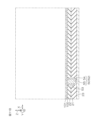
- FIG. 5 is an enlarged view of region V shown in FIG. 6A is an enlarged view of a part of the top wiring shown in FIG. 5.
- FIG. 6B is an enlarged view of a portion of the pad structure shown in FIG. 5.
- FIG. FIG. 7 is a graph showing the relationship between the thickness of the wiring electrode and the stress.
- FIG. 8 is a graph showing the relationship between the thickness of the first metal film and stress.
- FIG. 9 is a graph showing the relationship between the overlap width of the base resin film and the stress.
- FIG. 10 is a graph showing the relationship between the thickness of the underlying resin film and the stress.
- 11A is a cross-sectional view showing an example of a method of manufacturing the package shown in FIG. 1.
- FIG. 11B is a cross-sectional view showing a step after the step of FIG. 11A.
- FIG. 11C is a cross-sectional view showing a step after the step of FIG. 11B.
- FIG. 11D is a cross-sectional view showing a step after the step of FIG. 11C.
- FIG. 11E is a cross-sectional view showing a step after the step of FIG.
- FIG. 11F is a cross-sectional view showing a step after the step of FIG. 11E.
- FIG. 11G is a cross-sectional view showing a step after the step of FIG. 11F.
- FIG. 11H is a cross-sectional view showing a step after the step of FIG. 11G.
- FIG. 11I is a cross-sectional view showing a step after the step of FIG. 11H.
- FIG. 11J is a cross-sectional view showing a step after the step of FIG. 11I.
- FIG. 11K is a cross-sectional view showing a step after the step of FIG. 11J.
- FIG. 11L is a cross-sectional view showing a step after the step of FIG. 11K.
- FIG. 11M is a cross-sectional view showing a step after the step of FIG. 11L.
- FIG. 11N is a cross-sectional view showing a step after the step of FIG. 11M.
- FIG. 11O is a cross-sectional view showing a step after the step of FIG. 11N.
- FIG. 11P is a cross-sectional view showing a step after the step of FIG. 11O.
- FIG. 11Q is a cross-sectional view showing a step after the step of FIG. 11P.
- FIG. 11R is a cross-sectional view showing a step after the step of FIG. 11Q.
- FIG. 11S is a cross-sectional view showing a step after the step of FIG. 11R.
- FIG. 12 is a cross-sectional view corresponding to FIG.
- FIG. 13A is a cross-sectional view showing an example of a manufacturing process of the electronic component shown in FIG. 12.
- FIG. 13B is a cross-sectional view showing a step after the step of FIG. 13A.
- FIG. 13C is a cross-sectional view showing a step after the step of FIG. 13B.
- FIG. 13D is a cross-sectional view showing a step after the step of FIG. 13C.
- FIG. 13E is a cross-sectional view showing a step after the step of FIG. 13D.
- FIG. 13F is a cross-sectional view showing a step after the step of FIG. 13E.
- FIG. 13G is a cross-sectional view showing a step after the step of FIG. 13F.
- FIG. 14 is a cross-sectional view corresponding to FIG. 4 and showing a package in which an electronic component according to the third embodiment is mounted.
- FIG. 15 is an enlarged view of region XV shown in FIG.
- FIG. 1 is a perspective view showing a package 2A mounted with an electronic component 1A according to the first embodiment.
- FIG. 2 is a plan view of the package 2A shown in FIG. 1 as viewed from the mounting surface 4 side.
- FIG. 3 is a plan view of the internal structure of the package 2A shown in FIG. 1 as viewed from the non-mounting surface 5 side.
- FIG. 4 is a cross-sectional view taken along line IV-IV shown in FIG.
- FIG. 5 is an enlarged view of region V shown in FIG.
- FIG. 6A is an enlarged view of a portion of the top wiring 25 shown in FIG.
- FIG. 6B is an enlarged view of a portion of the pad structure 65 shown in FIG. Hatching is omitted in FIGS. 6A and 6B for clarity.
- the package 2A is of the QFN (Quad Flat Non-leaded) type in this embodiment.
- the package 2A includes a hexahedral (rectangular parallelepiped in this embodiment) package body 3 .
- the package body 3 has a mounting surface 4 on one side, a non-mounting surface 5 on the other side, and first to fourth side walls 6A to 6D connecting the mounting surface 4 and the non-mounting surface 5, respectively.
- the mounting surface 4 and the non-mounting surface 5 are each formed in a quadrilateral shape when viewed from the normal direction Z (hereinafter simply referred to as "plan view").
- the first to fourth side walls 6A to 6D extend vertically along the normal direction Z.
- the first side wall 6A and the second side wall 6B extend in the first direction X along the mounting surface 4 and face the second direction Y intersecting (specifically, perpendicular to) the first direction X.
- the third side wall 6C and the fourth side wall 6D extend in the second direction Y and face the first direction X.
- the package body 3 includes a mold resin 7.
- Mold resin 7 includes a matrix resin and a plurality of fillers.
- the matrix resin may contain a thermosetting resin (eg, epoxy resin).
- the matrix resin may be colored with a coloring material such as carbon black. That is, the mold resin 7 may be an opaque resin.
- the multiple fillers are each made of spherical objects made of ceramics, oxides, insulators, etc.
- the plurality of fillers in this form, are each composed of silicon oxide particles (silica particles).
- Mold resin 7 preferably contains a plurality of fillers with different particle sizes.
- the package 2A includes a conductor plate 8 arranged inside the package body 3 .
- the conductor plate 8 may be called a "lead frame".
- the conductor plate 8 in this embodiment includes a die pad portion 9 , at least one (in this embodiment, a plurality of) lead portions 10 , and at least one (in this embodiment, a plurality of) finger portions 11 .
- the number of lead portions 10 is arbitrary.
- the presence or absence of finger portions 11 is optional, and a conductor plate 8 without finger portions 11 may be employed.
- the die pad portion 9 is arranged in the central portion of the package body 3 so as to be exposed from the mounting surface 4 .
- the die pad portion 9 is formed in a polygonal shape (specifically, a rectangular shape) having four sides parallel to the first to fourth side walls 6A to 6D in plan view.
- the planar shape of the die pad portion 9 is arbitrary.
- the die pad portion 9 has a protruding portion 9a protruding toward the first to fourth side walls 6A to 6D at the peripheral edge portion on the non-mounting surface 5 side.
- a plurality of lead portions 10 are arranged on the peripheral portion of the package body 3 with a gap from the die pad portion 9 so as to be exposed from the mounting surface 4 .
- the plurality of lead portions 10 need only be arranged along at least one of the first to fourth side walls 6A to 6D.
- a plurality (seven in this embodiment) of lead portions 10 are arranged along each of the first to fourth sidewalls 6A to 6D and are exposed from the corresponding first to fourth sidewalls 6A to 6D, respectively. ing.
- the plurality of lead portions 10 are each formed in a strip shape extending in a direction perpendicular to the corresponding first to fourth side walls 6A to 6D in plan view.
- the planar shape of the plurality of lead portions 10 is arbitrary.
- the plurality of lead portions 10 has projecting portions 10a projecting toward the die pad portion 9 (projecting portion 9a) at peripheral edge portions on the non-mounting surface 5 side.
- the plurality of finger portions 11 are drawn out from the die pad portion 9 toward the peripheral edges (first to fourth side walls 6A to 6D) of the package body 3 in plan view. That is, the finger portions 11 are fixed to the same potential as the die pad portion 9 . In this embodiment, the plurality of finger portions 11 are pulled out from the four corners of the die pad portion 9 toward the four corners of the package body 3 in plan view, and are exposed from the four corners of the package body 3 .
- the package 2A includes an electronic component 1A arranged inside the package body 3 so as to be electrically connected to the conductor plate 8.
- the electronic component 1A is arranged in a region on the non-mounting surface 5 side with respect to the conductor plate 8 so as not to be exposed from the package body 3 . That is, the entire outer surface of the electronic component 1A is covered with the mold resin 7. As shown in FIG.
- the electronic component 1A is mechanically and electrically connected to the conductor plate 8 by a flip chip connection method in this embodiment.
- the electronic component 1A is arranged inside the package body 3 so as to overlap the entire die pad portion 9, the ends of the plurality of lead portions 10, and the plurality of finger portions 11 in plan view.
- the electronic component 1A is mechanically and electrically connected to the die pad portion 9 and the ends of the plurality of lead portions 10, and is not mechanically connected to the plurality of finger portions 11.
- FIG. A specific structure of the electronic component 1A mounted in the package 2A will be described below.
- the electronic component 1A is a semiconductor device including a semiconductor chip 13 (chip).
- Semiconductor chip 13 may include at least one of silicon and a wide bandgap semiconductor.
- a wide bandgap semiconductor is a semiconductor that has a bandgap that exceeds that of silicon.
- Gallium nitride, silicon carbide, and diamond are examples of wide bandgap semiconductors.
- the semiconductor chip 13 consists of a silicon chip in this form.
- Semiconductor chip 13 may have a laminated structure including a semiconductor substrate and an epitaxial layer.
- the semiconductor chip 13 may have a single layer structure consisting of a semiconductor substrate or an epitaxial layer.
- the semiconductor chip 13 has a first main surface 14 on one side, a second main surface 15 on the other side, and first to fourth side surfaces 16A to 16D connecting the first main surface 14 and the second main surface 15. are doing.
- the first major surface 14 may also be referred to as the "terminal surface” or the “device surface”.
- the second major surface 15 may also be referred to as a "non-terminal surface” or “non-device surface.”
- the first main surface 14 and the second main surface 15 are formed in a square shape in plan view.
- the first side surface 16A and the second side surface 16B extend in the first direction X and face the second direction Y.
- the third side surface 16C and the fourth side surface 16D extend in the second direction Y and face the first direction X.
- the semiconductor chip 13 is disposed on the side of the non-mounting surface 5 with respect to the conductor plate 8 with the first main surface 14 facing the conductor plate 8 .
- the electronic component 1A includes a plurality of device regions 17 partitioned on the first main surface 14.
- multiple device regions 17 are indicated by dashed lines.
- the number and arrangement of the plurality of device regions 17 are arbitrary.
- the plurality of device regions 17 each include functional devices formed using regions inside and outside the semiconductor chip 13 .
- the functional device may include at least one of a semiconductor switching device, a semiconductor rectifying device and a passive device.
- a functional device may include a network of combined at least two of a semiconductor switching device, a semiconductor rectifying device and a passive device.
- the semiconductor switching device may include at least one of MISFET (Metal Insulator Semiconductor Field Effect Transistor), BJT (Bipolar Junction Transistor), IGBT (Insulated Gate Bipolar Junction Transistor) and JFET (Junction Field Effect Transistor) .
- MISFET Metal Insulator Semiconductor Field Effect Transistor
- BJT Bipolar Junction Transistor
- IGBT Insulated Gate Bipolar Junction Transistor
- JFET Joint Field Effect Transistor
- the semiconductor rectifier device may include at least one of a pn junction diode, a pin junction diode, a Zener diode, a Schottky barrier diode and a fast recovery diode.
- Passive devices may include at least one of resistors, capacitors, inductors and fuses.
- the electronic component 1A includes an insulating layer 20 formed on the first main surface 14. That is, the insulating layer 20 is interposed between the conductor plate 8 and the first principal surface 14 . In this embodiment, the insulating layer 20 covers the entire area of the first main surface 14 in plan view, and continues to the peripheral edge (first to fourth side surfaces 16A to 16D) of the semiconductor chip 13 .
- the insulating layer 20 includes a plurality of interlayer insulating films 21 and top insulating films 22 (to be covered).
- the number of layers of the plurality of interlayer insulating films 21 is arbitrary. As an example, the number of layers of the interlayer insulating film 21 may be 2 or more and 25 or less.
- Each of the plurality of interlayer insulating films 21 may have a single layer structure or a laminated structure including at least one of a silicon oxide film and a silicon nitride film.
- the plurality of interlayer insulating films 21 each have a single-layer structure made of a silicon oxide film in this embodiment.
- the top insulating film 22 forms a terminal insulating film of the insulating layer 20 and covers the uppermost interlayer insulating film 21 .
- the top insulating film 22 may be called an "inorganic insulating film” or a "passivation film”.
- the top insulating film 22 may have a single layer structure including at least one of a silicon oxide film and a silicon nitride film.
- the top insulating film 22 preferably contains an insulating material different from at least the uppermost interlayer insulating film 21 .
- the top insulating film 22 has a single-layer structure made of a silicon nitride film in this embodiment.
- Top insulating film 22 has a flat surface extending along first main surface 14 .
- the top insulating film 22 preferably has a thickness at least less than the thickness of the uppermost interlayer insulating film 21 .
- the thickness of the top insulating film 22 is less than the thickness of each interlayer insulating film 21 in this embodiment.
- the electronic component 1A includes a plurality of interlayer wirings 23 arranged within the insulating layer 20 .
- a plurality of interlayer wirings 23 are wiring films arranged on an arbitrary interlayer insulating film 21 in a layer below the top insulating film 22 .
- the routing form of the plurality of interlayer wirings 23 is arbitrary.
- a plurality of interlayer wirings 23 form a multilayer wiring structure 24 (to be covered) together with a plurality of interlayer insulating films 21 .
- the plurality of interlayer wirings 23 may include at least one of an Al-based metal film and a Cu-based metal film.
- the plurality of interlayer wirings 23 are composed of at least one of a pure Al film (an Al film with a purity of 99% or higher), a pure Cu film (a Cu film with a purity of 99% or higher), an AlCu alloy film, an AlSi alloy film, and an AlSiCu alloy film. may contain one.
- the electronic component 1A includes a plurality of top wirings 25 arranged on the insulating layer 20 (specifically, the top insulating film 22).
- a plurality of top wirings 25 form terminal wirings of the multilayer wiring structure 24 respectively.
- the routing form of the plurality of top wirings 25 is arbitrary.
- the plurality of top wirings 25 may be routed in a line shape in a plan view, or may be formed in an island shape.
- the plurality of top wirings 25 may have relatively wide island portions in a plan view and relatively narrow line portions extending in a line form from the island portions.
- the plurality of top wirings 25 each have a thickness exceeding the thickness of the top insulating film 22 . It is preferable that each of the plurality of top wirings 25 has a thickness exceeding the thickness of each interlayer wiring 23 . It is preferable that the plurality of top wirings 25 have a thickness less than the thickness of some of the plurality of fillers contained in the mold resin 7 .
- a plurality of wiring layers have the same configuration except for the arrangement location and routing form. The structure of one top wiring 25 will be specifically described below.
- top wiring 25 includes a wiring barrier film 30 that selectively covers top insulating film 22 .
- the wiring barrier film 30 extends substantially flat along the top insulating film 22 .
- the wiring barrier film 30 is made of a hard metal film having a relatively small coefficient of thermal expansion.
- the thermal expansion coefficient of the wiring barrier film 30 may be 4 ⁇ m/m ⁇ K or more and 9 ⁇ m/m ⁇ K or less.
- the wiring barrier film 30 preferably includes at least one of Ti film, TiN film, Ta film, W film, Mo film, Cr film and Ru film.
- the wiring barrier film 30 preferably contains a Ti-based metal.
- the wiring barrier film 30 may have a laminated structure or a single layer structure including at least one of a Ti film and a TiN film.
- the wiring barrier film 30 may have a laminated structure including a Ti film and a TiN film laminated in this order from the top insulating film 22 side.
- the wiring barrier film 30 has a single-layer structure made of a Ti film in this embodiment.
- the wiring barrier film 30 has a first thickness T1 in the stacking direction.
- the stacking direction is the normal direction Z (same hereafter).
- the first thickness T1 may be 0.01 ⁇ m or more and 0.5 ⁇ m or less.
- the first thickness T1 is preferably 0.05 ⁇ m or more and 0.2 ⁇ m or less.
- the top wiring 25 includes wiring electrodes 31 covering the wiring barrier film 30 .
- the wiring electrode 31 forms the main body of the top wiring 25 .
- the wiring electrode 31 includes a metal film different from the wiring barrier film 30 .
- the wiring electrode 31 specifically includes a low-hardness metal film having a thermal expansion coefficient exceeding that of the wiring barrier film 30 .
- the wiring electrode 31 may include at least one of an Al-based metal film and a Cu-based metal film.
- the wiring electrode 31 is at least one of a pure Al film (an Al film with a purity of 99% or more), a pure Cu film (a Cu film with a purity of 99% or more), an AlCu alloy film, an AlSi alloy film, or an AlSiCu alloy film. may contain
- the wiring electrode 31 is preferably made of a Cu-based metal film.
- the wiring electrode 31 consists of a pure Cu film
- the thermal expansion coefficient of the wiring electrode 31 is about 16.5 ⁇ m/m ⁇ K in this form.
- the wiring electrode 31 has a second thickness T2 (T1 ⁇ T2) that exceeds the first thickness T1 of the wiring barrier film 30 in the stacking direction.
- the second thickness T2 may be 1 ⁇ m or more and 15 ⁇ m or less.
- the wiring electrode 31 covers the entire wiring barrier film 30 in cross-sectional view and plan view.
- the wiring electrode 31 has a peripheral portion projecting outside the wiring barrier film 30 so as to face the top insulating film 22 in the stacking direction.
- the wiring electrode 31 includes a wiring lower surface 32 , a wiring upper surface 33 and wiring sidewalls 34 .
- the wiring lower surface 32 extends substantially flat along the wiring barrier film 30 .
- the wiring upper surface 33 extends substantially flat along the wiring barrier film 30 .
- the wiring sidewall 34 is located on the top insulating film 22 and extends substantially vertically in the stacking direction. "Substantially vertical” also includes a form extending in the stacking direction while curving (meandering).
- the wiring sidewall 34 is positioned outside the wiring barrier film 30 and faces the top insulating film 22 without the wiring barrier film 30 interposed therebetween in the stacking direction.
- the wiring sidewall 34 has a wiring upper end portion 35 on the wiring upper surface 33 side and a wiring lower end portion 36 on the top insulating film 22 side.
- the wiring sidewall 34 has a wiring recess portion 37 recessed inwardly at the wiring lower end portion 36 .
- the wiring recess portion 37 forms an uneven portion (wiring uneven portion) at the wiring lower end portion 36 .
- the wiring recess portion 37 may be recessed inwardly from the wiring upper end portion 35 .
- the wiring recess portion 37 may be recessed in a curved shape.
- the wiring recess portion 37 exposes the peripheral portion of the wiring barrier film 30 .
- the wiring recess portion 37 has an upper end located outside the peripheral edge of the wiring barrier film 30 and a lower end located inside the peripheral edge of the wiring barrier film 30 .
- the wiring recess portion 37 also exposes the top insulating film 22 in this embodiment.
- the wiring recess portion 37 is formed with a space from the intermediate portion of the wiring side wall 34 toward the top insulating film 22 side.
- the wiring recess portion 37 has a first longitudinal width W1 (T1 ⁇ W1) that exceeds the first thickness T1 of the wiring barrier film 30 in the stacking direction.
- the first vertical width W1 may be 0.01 ⁇ m or more and 1 ⁇ m or less.
- the first vertical width W1 is preferably 0.5 ⁇ m or less.
- the wiring recess portion 37 has a first lateral width W2 (T1 ⁇ W2) exceeding the first thickness T1 in the directions perpendicular to the stacking direction (the first direction X and the second direction Y).
- the first width W2 may be 0.01 ⁇ m or more and 1 ⁇ m or less.
- the first width W2 is preferably 0.5 ⁇ m or less.
- the wiring electrode 31 has a wiring upper end corner portion 38 formed in a round shape.
- the wiring upper end corner portion 38 is a corner portion that connects the wiring upper surface 33 and the wiring side wall 34 (the wiring upper end portion 35). That is, the wiring upper end corner portion 38 connects the wiring upper surface 33 and the wiring side wall 34 in an arc shape (curved shape). That is, the wiring upper end corner portion 38 is inclined obliquely downward in an arc shape from the wiring upper surface 33 toward the wiring side wall 34 at the peripheral edge portion of the wiring upper surface 33 .
- the center of curvature of the arc is positioned either inside the wiring electrode 31 or inside the interlayer insulating film 21 (top insulating film 22).
- the wiring top corner portion 38 includes a portion facing the wiring barrier film 30 in the stacking direction and a portion not facing the wiring barrier film 30 .
- the width of the portion of the wiring top corner portion 38 that does not face the wiring barrier film 30 is less than the width of the portion of the wiring top corner portion 38 that faces the wiring barrier film 30 .
- the wiring upper end corner portion 38 has a round start point P1 and a round end point P2.
- the round starting point P1 is positioned on the wiring upper surface 33 side.
- the round end point P2 is located on the wiring side wall 34 side.
- the wiring upper end corner portion 38 has a round width WR in the direction orthogonal to the stacking direction.
- the round width WR is the distance between the round start point P1 and the round end point P2 in the direction orthogonal to the stacking direction.
- the round width WR preferably exceeds the first lateral width W2 of the wiring recess portion 37 (W2 ⁇ WR). Also, the round width WR preferably exceeds the first vertical width W1 of the wiring recess portion 37 (W1 ⁇ WR).
- the round width WR is preferably less than the second thickness T2 of the wiring electrode 31 (WR ⁇ T2).
- the round width WR may be 1 ⁇ m or more and 20 ⁇ m or less.
- a first virtual line L1 and a second virtual line L2 are set in the vicinity of the upper end corner portion 38 of the wiring.
- the first virtual line L ⁇ b>1 is a virtual line extending along the wiring upper surface 33 .
- the second virtual line L2 is a virtual line that connects the round start point P1 and the round end point P2.
- the wiring upper end corner portion 38 is such that the angle ⁇ between the first virtual line L1 and the second virtual line L2 exceeds 0° and is 45° or less. It is preferably formed to belong to the range. In this embodiment, the wiring upper end corner portion 38 is formed so that the angle ⁇ falls within the range of 10° or more and 30° or less.
- the top wiring 25 includes wiring cover electrodes 41 that cover the wiring electrodes 31 .
- the wiring cover electrode 41 includes a conductor different from the wiring electrode 31 and covers the entire wiring electrode 31 in a film form.
- the wiring cover electrode 41 has a third thickness T3 (T3 ⁇ T2) less than the second thickness T2 of the wiring electrode 31 in the stacking direction.
- the third thickness T3 may be 0.55 ⁇ m or more and 11 ⁇ m or less.
- the third thickness T3 is preferably 1.1 ⁇ m or more and 2.5 ⁇ m or less.
- the third thickness T3 preferably has a thickness less than the thickness of some of the multiple fillers contained in the mold resin 7 .
- the wiring cover electrode 41 has a first lower surface 42 , a first upper surface 43 , and a first peripheral wall 44 connecting the first lower surface 42 and the first upper surface 43 .
- the first bottom surface 42 extends along the wiring top surface 33
- the first top surface 43 extends along the wiring top surface 33 .
- the first peripheral wall 44 is a side wall of the wiring cover electrode 41 and extends substantially vertically along the stacking direction. "Substantially vertical" also includes a form extending in the stacking direction while curving (meandering).
- the wiring cover electrode 41 includes a round portion 45 that covers the upper corner portion 38 of the wiring in a film shape so as to curve along the upper corner portion 38 of the wiring. That is, the round portion 45 is formed in a film shape so that the first lower surface 42 and the first upper surface 43 are curved along the wiring upper end corner portion 38 . Further, the round portion 45 is formed so as to incline downward in an arc shape from the wiring upper surface 33 side toward the wiring side wall 34 side. The round portion 45 covers the entire area between the round start point P1 and the round end point P2 at the upper end corner portion 38 of the wiring. The round portion 45 forms a round end portion P2 at the connection portion with the wiring side wall 34 .
- the wiring cover electrode 41 further has a first extending portion 46 extending to a region outside the wiring cover electrode 41 (wiring upper end corner portion 38).
- the first extending portion 46 forms the peripheral portion of the wiring cover electrode 41 and is composed of the first lower surface 42 , the first upper surface 43 and the first peripheral wall 44 .
- the first extending portion 46 is formed in an arc shape continuously extending from the round portion 45 and has a portion located closer to the top insulating film 22 than the wiring upper surface 33 .
- the first extension 46 faces the top insulating film 22 in the stacking direction, and faces the wiring electrode 31 (wiring side wall 34) in the direction perpendicular to the stacking direction.
- the first extended portion 46 has a lower end located between the wiring upper surface 33 and the top insulating film 22 .
- the lower end portion of the first extending portion 46 is formed by the connecting portion of the first lower surface 42 extending in an arc shape and the first peripheral wall 44 extending substantially vertically, and has a sharp shape forming an acute angle in a cross-sectional view.
- the first extending portion 46 has a first extending width W3 in the direction perpendicular to the stacking direction.
- the first extension width W3 preferably exceeds the first vertical width W1 of the wiring recess portion 37 (W1 ⁇ W3).
- the first extension width W3 preferably exceeds the first lateral width W2 of the wiring recess portion 37 (W2 ⁇ W3).
- the first extending width W3 is preferably less than the round width WR (W3 ⁇ WR).
- the first extension width W3 is preferably equal to or less than the third thickness T3 of the wiring cover electrode 41 (W3 ⁇ T3). Of course, the first extension width W3 may exceed the third thickness T3 of the wiring cover electrode 41 (T3 ⁇ W3).
- the wiring cover electrode 41 has a laminated structure in which a plurality of metal films are laminated.
- the wiring cover electrode 41 includes a first metal film 47 and a second metal film 48 laminated in this order from the wiring electrode 31 side.
- the first metal film 47 covers the entire wiring upper surface 33 in a film shape, and forms part of the first lower surface 42 and the first peripheral wall 44 of the wiring cover electrode 41 .
- the first metal film 47 includes a metal film with hardness higher than that of the wiring electrode 31 .
- the first metal film 47 preferably contains a Ni-based metal film.
- the first metal film 47 includes a pure Ni film (a Ni film with a purity of 99% or higher) in this embodiment.
- the first metal film 47 has a fourth thickness T4.
- the fourth thickness T4 may be 0.5 ⁇ m or more and 6 ⁇ m or less.
- the second metal film 48 covers the entire area of the second metal film 48 in a film form, and forms part of the first upper surface 43 and the first peripheral wall 44 of the wiring cover electrode 41 .
- the second metal film 48 preferably contains a Pd-based metal film.
- the second metal film 48 includes a pure Pd film (a Pd film with a purity of 99% or higher) in this embodiment.
- the second metal film 48 has a fifth thickness T5 less than the fourth thickness T4 of the first metal film 47 (T5 ⁇ T4).
- the fifth thickness T5 may be 0.05 ⁇ m or more and 1 ⁇ m or less.
- the fifth thickness T5 is preferably 0.1 ⁇ m or more and 0.5 ⁇ m or less.
- the total value of the fourth thickness T4 and the fifth thickness T5 is the third thickness T3.
- electronic component 1A includes a plurality of via electrodes 50 arranged in insulating layer 20.
- the plurality of via electrodes 50 includes a plurality of first via electrodes 51 arranged within the interlayer insulating film 21 and a plurality of second via electrodes 52 arranged within the top insulating film 22 .
- a plurality of first via electrodes 51 penetrate the corresponding interlayer insulating films 21 so as to electrically connect a plurality of arbitrary interlayer wirings 23 facing each other in the stacking direction.
- a plurality of second via electrodes 52 respectively penetrate the top insulating film 22 and the uppermost interlayer insulating film 21 so as to electrically connect arbitrary interlayer wirings 23 and arbitrary top wirings 25 facing each other in the stacking direction. .
- a plurality of via electrodes 50 are embedded in via holes 53 formed in the insulating layer 20 respectively.
- a plurality of via electrodes 50 each have a laminated structure including a via barrier film 54 and a via body 55 .
- the via barrier film 54 coats the inner wall of the via hole 53 in a film form.
- the via barrier film 54 may contain a Ti-based metal film.
- the via body 55 is embedded in the via hole 53 with the via barrier film 54 interposed therebetween. Via body 55 may include tungsten.
- electronic component 1A includes base resin film 60 (organic film) formed on insulating layer 20. As shown in FIG. That is, the underlying resin film 60 is interposed between the conductor plate 8 and the multilayer wiring structure 24 .
- the underlying resin film 60 has an elastic modulus lower than that of the top insulating film 22 and is relatively soft.
- the underlying resin film 60 is made of a resin material different from the mold resin 7 described above.
- the underlying resin film 60 specifically contains a photosensitive resin (that is, a transparent resin).
- Base resin film 60 may include at least one of an epoxy resin film, a polyimide resin film, a polyamide resin film, a polybenzoxazole resin film, and a phenol resin film.
- the underlying resin film 60 has a single-layer structure made of a phenolic resin film in this embodiment.
- the base resin film 60 is spaced inwardly from the peripheral edge (first to fourth side surfaces 16A to 16D) of the insulating layer 20 in plan view, and exposes the peripheral edge of the insulating layer 20. As shown in FIG.
- the base resin film 60 covers the wiring sidewalls 34 of the wiring electrodes 31 in the regions between the plurality of top wirings 25 on the insulating layer 20 .
- the underlying resin film 60 fills the wiring recess portion 37 at the wiring lower end portion 36 of the wiring side wall 34 .
- the underlying resin film 60 is in contact with the top insulating film 22 , the wiring barrier film 30 and the wiring electrode 31 within the wiring recess portion 37 .
- the base resin film 60 fills the gap between the wiring side wall 34 and the first extending portion 46 of the wiring cover electrode 41 at the wiring upper end portion 35 of the wiring side wall 34 . That is, the underlying resin film 60 is in contact with the wiring sidewall 34 of the wiring electrode 31 and the first lower surface 42 of the wiring cover electrode 41 on the wiring upper end portion 35 side.
- the underlying resin film 60 includes an overlapping portion 61 covering the first upper surface 43 of the wiring cover electrode 41 .
- the overlap portion 61 extends inwardly of the first upper surface 43 from the first peripheral wall 44 .
- the overlapping portion 61 defines a pad opening 62 that partially exposes the wiring cover electrode 41 in the inner portion of the wiring cover electrode 41 .
- the overlap portion 61 covers the wiring upper end corner portion 38 of the wiring electrode 31 with the wiring cover electrode 41 interposed therebetween.
- the overlap portion 61 preferably covers the entire round portion 45 of the wiring cover electrode 41 .
- the overlap portion 61 preferably covers the entire region between the round start portion P1 and the round end portion P2 of the wiring electrode 31 with the wiring cover electrode 41 interposed therebetween.
- the overlap portion 61 has an overlap width WO (WR ⁇ WO) equal to or larger than the round width WR in the direction orthogonal to the stacking direction.
- the overlap width WO may be 1 ⁇ m or more and 40 ⁇ m or less.
- the overlap width WO may exceed the second thickness T2 of the wiring electrode 31 (T2 ⁇ WO), or may be equal to or less than the second thickness T2 (WO ⁇ T2).
- the overlap portion 61 has a sixth thickness T6 in the stacking direction.
- the sixth thickness T6 may be 1 ⁇ m or more and 40 ⁇ m or less.
- the sixth thickness T6 may exceed the third thickness T3 of the wiring cover electrode 41 (T3 ⁇ T6).
- the sixth thickness T6 may exceed the round width WR (WR ⁇ T6).
- the sixth thickness T6 may exceed the second thickness T2 (T2 ⁇ T6) or may be equal to or less than the second thickness T2 (T6 ⁇ T2).
- the sixth thickness T6 preferably has a thickness less than the thickness of some of the multiple fillers contained in the mold resin 7 .
- electronic component 1A has a plurality of pad structures 65 respectively arranged on corresponding top wirings 25 so as to be electrically connected to corresponding top wirings 25.
- a plurality of pad structures 65 are terminal electrodes interposed between the conductor plate 8 and the top wiring 25 to electrically connect the conductor plate 8 and the top wiring 25 .
- a specific structure of one pad structure 65 will be described below.
- the pad structure 65 includes a pad barrier film 70 selectively covering the top wiring 25 .
- the pad barrier film 70 covers the first upper surface 43 of the wiring cover electrode 41 and the overlapping portion 61 of the base resin film 60 in a film form. A portion of the pad barrier film 70 covering the overlap portion 61 is located above a portion of the pad barrier film 70 covering the first upper surface 43 .
- the pad barrier film 70 is made of a hard metal film having a relatively small coefficient of thermal expansion.
- Pad barrier film 70 includes at least one of Ti film, TiN film, Ta film, W film, Mo film, Cr film and Ru film.
- the coefficient of thermal expansion of the pad barrier film 70 may be 4 ⁇ m/m ⁇ K or more and 9 ⁇ m/m ⁇ K or less.
- the pad barrier film 70 preferably contains a Ti-based metal.
- the pad barrier film 70 may have a laminated structure or a single layer structure including at least one of a Ti film and a TiN film.
- the pad barrier film 70 may have a laminated structure including a Ti film and a TiN film laminated in this order from the top wiring 25 side.
- the pad barrier film 70 has a single layer structure made of a Ti film in this embodiment.
- the pad barrier film 70 has a seventh thickness T7 in the stacking direction.
- the seventh thickness T7 may be 0.01 ⁇ m or more and 0.5 ⁇ m or less.
- the seventh thickness T7 is preferably 0.05 ⁇ m or more and 0.2 ⁇ m or less.
- the pad barrier film 70 may have the same material and/or the same thickness as the wiring barrier film 30 .
- the pad structure 65 includes a pad electrode 71 covering the pad barrier film 70 .
- a pad electrode may be referred to as a "terminal electrode”.
- the pad electrode 71 forms the main body of the pad structure 65 and has a columnar shape standing along the stacking direction in a cross-sectional view.
- Pad electrode 71 includes a metal film different from pad barrier film 70 .
- Pad electrode 71 specifically includes a low-hardness metal film having a thermal expansion coefficient exceeding that of pad barrier film 70 .
- the pad electrode 71 may include at least one of an Al-based metal film and a Cu-based metal film.
- the pad electrode 71 is at least one of a pure Al film (an Al film with a purity of 99% or more), a pure Cu film (a Cu film with a purity of 99% or more), an AlCu alloy film, an AlSi alloy film, and an AlSiCu alloy film. may contain
- the pad electrode 71 is preferably made of a Cu-based metal film.
- the pad electrode 71 consists of a pure Cu film in this form.
- the coefficient of thermal expansion of the pad electrode 71 is approximately 16.5 ⁇ m/m ⁇ K in this embodiment.
- the pad electrode 71 has an eighth thickness T8 (T7 ⁇ T8) that exceeds the seventh thickness T7 of the pad barrier film 70 in the stacking direction.
- the eighth thickness T8 is the thickness of the pad electrode 71 with the top wiring 25 (wiring cover electrode 41) as a reference (zero point).
- the eighth thickness T8 exceeds the second thickness T2 of the wiring electrode 31 (T2 ⁇ T8).
- the eighth thickness T8 is preferably less than the thickness of the conductor plate 8.
- the eighth thickness T8 preferably exceeds the sixth thickness T6 of the underlying resin film 60 (overlapping portion 61) (T6 ⁇ T8).
- the eighth thickness T8 may be 10 ⁇ m or more and 100 ⁇ m or less.
- the eighth thickness T8 is preferably 20 ⁇ m or more and 60 ⁇ m or less.
- the eighth thickness T8 preferably has a thickness exceeding the thickness of the plurality of fillers contained in the molding resin 7. As shown in FIG.
- the pad electrode 71 covers the overlapping portion 61 of the base resin film 60 with a space inward from the wiring upper end corner portion 38 of the wiring electrode 31 in plan view. That is, the pad electrode 71 is spaced inwardly from the round portion 45 of the wiring cover electrode 41 and does not face the round portion 45 with the underlying resin film 60 (overlap portion 61) interposed therebetween.
- the pad electrode 71 enters the pad opening 62 from above the underlying resin film 60 (overlapping portion 61 ) and is connected to the wiring cover electrode 41 via the pad barrier film 70 within the pad opening 62 .
- the pad electrode 71 covers the entire pad barrier film 70 in cross-sectional view and plan view.
- the pad electrode 71 has a peripheral portion that protrudes outside the pad barrier film 70 and faces the underlying resin film 60 in the stacking direction.
- the pad electrode 71 includes a pad lower surface 72 , a pad upper surface 73 and pad sidewalls 74 .
- Pad lower surface 72 extends along first upper surface 43 of wiring cover electrode 41 and overlapping portion 61 of underlying resin film 60 .
- a portion of the pad lower surface 72 that covers the overlap portion 61 is located above a portion of the pad lower surface 72 that covers the first upper surface 43 .
- the pad upper surface 73 extends along the overlap portion 61 between the first upper surface 43 of the wiring cover electrode 41 and the underlying resin film 60 .
- a portion of the pad upper surface 73 that covers the first upper surface 43 is recessed toward the wiring cover electrode 41 . That is, the portion of the pad upper surface 73 that covers the overlap portion 61 is located above the portion of the pad upper surface 73 that covers the first upper surface 43 .
- the pad side wall 74 is located on the underlying resin film 60 and extends substantially vertically along the normal direction Z. As shown in FIG. "Substantially vertical" also includes a form extending in the stacking direction while curving (meandering). The pad sidewall 74 is positioned outside the pad barrier film 70 and faces the base resin film 60 in the stacking direction without the pad barrier film 70 interposed therebetween.
- the pad side wall 74 has a pad upper end portion 75 on the pad upper surface 73 side and a pad lower end portion 76 on the underlying resin film 60 side.
- the pad side wall 74 has a pad recess portion 77 recessed inwardly from the pad upper end portion 75 at the pad lower end portion 76 .
- the pad recess portion 77 forms an uneven portion (pad uneven portion) at the pad lower end portion 76 .
- the pad recess portion 77 may be recessed inwardly from the pad upper end portion 75 .
- the pad recess portion 77 may be recessed in a curved shape.
- the pad recess portion 77 exposes the peripheral portion of the pad barrier film 70 .
- the pad recess portion 77 has an upper end located outside the peripheral edge of the pad barrier film 70 and a lower end located inside the peripheral edge of the pad barrier film 70 .
- the pad recess portion 77 also exposes the base resin film 60 .
- the pad recess portion 77 is formed with a space from the intermediate portion of the pad side wall 74 toward the top wiring 25 side.
- the pad recess portion 77 has a second longitudinal width W4 (T7 ⁇ W4) that exceeds the seventh thickness T7 of the pad barrier film 70 in the stacking direction.
- the second vertical width W4 may be 0.01 ⁇ m or more and 1 ⁇ m or less.
- the second vertical width W4 is preferably 0.5 ⁇ m or less.
- the pad recess portion 77 has a second lateral width W5 (T7 ⁇ W5) that exceeds the seventh thickness T7 of the pad barrier film 70 in the direction orthogonal to the stacking direction.
- the second width W5 may be 0.01 ⁇ m or more and 1 ⁇ m or less.
- the second width W5 is preferably 0.5 ⁇ m or less.
- the pad electrode 71 has an angular pad upper corner 78 unlike the wiring upper corner 38 of the wiring electrode 31 .
- Pad upper end corner portion 78 is a corner portion connecting pad upper surface 73 and pad side wall 74 (pad upper end portion 75).
- the pad upper end corner portion 78 may have a sharp shape protruding upward at an acute angle in a cross-sectional view due to the depression.
- the wiring top corner portion 38 faces the base resin film 60 in the stacking direction without the pad barrier film 70 interposed therebetween.
- the pad electrode 71 includes a pad cover electrode 81 covering the pad electrode 71 .
- the pad cover electrode 81 contains a conductor different from the pad electrode 71 and covers the entire area of the pad electrode 71 in a film form.
- the pad cover electrode 81 has a ninth thickness T9 (T9 ⁇ T8) that is less than the eighth thickness T8 of the pad electrode 71 in the stacking direction.
- the ninth thickness T9 may be 0.5 ⁇ m or more and 6 ⁇ m or less.
- the ninth thickness T9 is preferably 1 ⁇ m or more and 5 ⁇ m or less.
- the ninth thickness T9 preferably has a thickness less than the thickness of some of the plurality of fillers contained in the mold resin 7 .
- the pad cover electrode 81 has a second lower surface 82 , a second upper surface 83 , and a second peripheral wall 84 connecting the second lower surface 82 and the second upper surface 83 .
- the second bottom surface 82 extends along the pad top surface 73 and the second top surface 83 extends along the pad top surface 73 .
- the second peripheral wall 84 is a side wall of the pad cover electrode 81 and extends substantially vertically along the stacking direction. "Substantially vertical" also includes a form extending in the stacking direction while curving (meandering).
- the pad cover electrode 81 has a second extending portion 86 extending to a region outside the pad cover electrode 81 (pad top corner portion 78).
- the second extended portion 86 forms the peripheral portion of the pad cover electrode 81 and is composed of the second lower surface 82 , the second upper surface 83 and the second peripheral wall 84 .
- the second extending portion 86 faces the top wiring 25 in the stacking direction.
- the angle formed by the second lower surface 82 of the pad cover electrode 81 and the second peripheral wall 84 exceeds the angle formed by the first lower surface 42 and the first peripheral wall 44 of the wiring cover electrode 41 .
- the second extending portion 86 has a second extending width W6 in the direction perpendicular to the stacking direction.
- the second extension width W6 preferably exceeds the second longitudinal width W4 of the pad recess portion 77 (W4 ⁇ W6).
- the second extension width W6 preferably exceeds the second lateral width W5 of the pad recess portion 77 (W5 ⁇ W6).
- the second extension width W6 is preferably equal to or less than the ninth thickness T9 of the pad cover electrode 81 (W6 ⁇ T9). Of course, the second extension width W6 may exceed the ninth thickness T9 of the pad cover electrode 81 (T9 ⁇ W6).
- the pad cover electrode 81 has a single layer structure consisting of a single third metal film 87 in this form.
- the third metal film 87 covers the entire area of the pad upper surface 73 in a film form, and forms the second lower surface 82 , the second upper surface 83 and the second peripheral wall 84 of the wiring cover electrode 41 .
- the third metal film 87 includes a metal film with hardness higher than that of the pad electrode 71 .
- the third metal film 87 preferably contains a Ni-based metal film.
- the third metal film 87 includes a pure Ni film (a Ni film with a purity of 99% or higher) in this embodiment.
- the pad structure 65 further includes a plurality of low melting point metals 90 each arranged on the corresponding pad electrode 71 so as to be electrically connected to the corresponding pad electrode 71 .
- Low melting point metal 90 is interposed between conductor plate 8 and pad electrode 71 to mechanically and electrically connect conductor plate 8 and pad electrode 71 .
- the low melting point metal 90 is solder in this form.
- the low melting point metal 90 is preferably lead-free solder.
- the low melting point metal 90 is made of solder containing at least one of Sn and Ag in this form. The structure of one low melting point metal 90 is described below.
- the low melting point metal 90 is arranged on the pad upper surface 73 so as to expose the pad sidewalls 74 of the pad electrode 71 .
- the low melting point metal 90 fills the depression of the pad upper surface 73 above the pad cover electrode 81 .
- the low melting point metal 90 covers the entire area of the pad upper surface 73 in this form.
- the low melting point metal 90 covers the second extended portion 86 of the pad cover electrode 81 so as to expose the second peripheral wall 84 of the pad cover electrode 81 .
- the low melting point metal 90 may partially cover the second peripheral wall 84 so as to partially expose the second peripheral wall 84 .
- the low-melting-point metal 90 faces the underlying resin film 60 with the second extended portion 86 interposed therebetween.
- the low-melting-point metal 90 has a bulging portion 91 projecting outside the second extended portion 86 .
- the bulging portion 91 protrudes in an arc shape with the second extending portion 86 as a starting point.
- the bulging portion 91 faces the underlying resin film 60 without the second extending portion 86 interposed therebetween.
- the low melting point metal 90 has a tenth thickness T10 (T9 ⁇ T10) that exceeds the ninth thickness T9 in the stacking direction.
- a tenth thickness T10 is the maximum thickness of the low melting point metal 90 .
- the tenth thickness T10 preferably exceeds the second thickness T2 of the wiring electrode 31 (T2 ⁇ T10).
- the tenth thickness T10 may be equal to or less than the eighth thickness T8 (T10 ⁇ T8) of the pad electrode 71, or may exceed the eighth thickness T8 (T8 ⁇ T10).
- the tenth thickness T ⁇ b>10 is preferably less than the thickness of the conductor plate 8 .
- the tenth thickness T10 preferably has a thickness less than the thickness of some of the plurality of fillers contained in the mold resin 7 .
- electronic component 1A includes top resin 95 that coats bottom resin film 60 .
- the overlying resin 95 is made of a resin material different from that of the underlying resin film 60 .
- the overlying resin 95 has an elastic modulus higher than that of the underlying resin film 60 and a hardness higher than that of the underlying resin film 60 .
- the overlying resin 95 consists of a part of the above-mentioned mold resin 7 in this form.
- the top resin 95 is interposed between the conductor plate 8 and the base resin film 60 and covers the conductor plate 8 , the base resin film 60 , the plurality of pad electrodes 71 and the plurality of low melting point metals 90 . Further, the top resin 95 covers the peripheral portion of the insulating layer 20 exposed from the base resin film 60 .
- the overlying resin 95 covers the pad sidewalls 74 of the pad electrodes 71 in regions between the plurality of pad electrodes 71 on the underlying resin film 60 .
- the overlying resin 95 has a portion covering the top insulating film 22 with the underlying resin film 60 interposed therebetween.
- the overlying resin 95 has a portion covering the wiring upper end corner portion 38 of the wiring electrode 31 with the underlying resin film 60 interposed therebetween.
- the overlying resin 95 fills the pad recess portion 77 at the pad lower end portion 76 of the pad side wall 74 .
- the overlying resin 95 is in contact with the underlying resin film 60 , the pad barrier film 70 and the pad electrode 71 in the pad recess portion 77 .
- the upper base resin 95 is in contact with the pad side wall 74 and the second extending portion 86 (second lower surface 82 ) of the pad cover electrode 81 at the pad upper end portion 75 of the pad side wall 74 .
- the top resin 95 covers the second peripheral wall 84 and the low melting point metal 90 of the pad electrode 71 and does not cover the second upper surface 83 of the pad electrode 71 .
- the electronic component 1A includes the semiconductor chip 13, the multilayer wiring structure 24 (insulating layer 20), the pad structure 65 (a plurality of pad electrodes 71) and a plurality of low melting point metals 90.
- the electronic component 1A is arranged in the package body 3 with the pad structure 65 facing the conductor plate 8.
- a plurality of pad electrodes 71 are joined to corresponding locations (die pad portion 9 or lead portion 10 ) of conductor plate 8 via corresponding low-melting-point metals 90 .
- the electric signal from the conductor plate 8 is applied to the electronic component 1A, and the electric signal from the electronic component 1A is applied to the conductor plate 8.
- FIG. 7 is a graph showing the relationship between the second thickness T2 of the wiring electrode 31 and stress.
- the vertical axis indicates the stress [Mpa]
- the horizontal axis indicates the second thickness T2 [ ⁇ m].
- the graph of FIG. 7 shows the stress when the second thickness T2 is changed from 4 ⁇ m to 14 ⁇ m.
- the stress varies depending on the second thickness T2. Specifically, the stress increases with increasing second thickness T2. Therefore, the smaller the second thickness T2, the better. However, reducing the second thickness T2 increases the resistance value. Therefore, the second thickness T2 is preferably 6 ⁇ m or more and 12 ⁇ m or less. It is particularly preferable that the second thickness T2 is 10 ⁇ m or less. In this case, stress caused by the second thickness T2 can be suppressed to 300 Mpa or less while suppressing an increase in resistance value.
- FIG. 8 is a graph showing the relationship between the fourth thickness T4 of the first metal film 47 and stress.
- the vertical axis indicates the stress [Mpa]
- the horizontal axis indicates the fourth thickness T4 [ ⁇ m].
- the graph of FIG. 8 shows the stress when the fourth thickness T4 is changed from 1 ⁇ m to 5 ⁇ m.
- the stress varies depending on the fourth thickness T4. Specifically, the stress increases as the fourth thickness T4 increases. Therefore, it is preferable that the fourth thickness T4 be as small as possible. However, if the fourth thickness T4 is reduced, the film formability of the first metal film 47 (especially the first extending portion 46) with respect to the wiring electrode 31 is lowered. Therefore, the fourth thickness T4 is preferably 1 ⁇ m or more and 3 ⁇ m or less. In this case, the stress caused by the fourth thickness T4 can be suppressed to 300 Mpa or less while suppressing the deterioration of the film formation properties.
- FIG. 9 is a graph showing the relationship between the overlap width WO of the base resin film 60 and stress.
- the vertical axis indicates the stress [Mpa] and the horizontal axis indicates the overlap width WO [ ⁇ m].
- the graph of FIG. 9 shows the stress when the overlap width WO is varied from 1 ⁇ m to 30 ⁇ m.
- the stress varies depending on the overlap width WO.
- the stress specifically decreases with increasing overlap width WO. Therefore, it is preferable that the overlap width WO is large. Also, by increasing the overlap width WO, the top wiring 25 can be properly protected.
- the overlap width WO is preferably 5 ⁇ m or more. It is particularly preferable that the overlap width WO is 10 ⁇ m or more.
- the stress caused by the overlap width WO can be suppressed to 300 Mpa or less while appropriately protecting the top wiring 25 .
- the overlap width WO is increased too much, the area of the exposed portion (pad opening 62) of the top wiring 25 is reduced.
- the upper limit of the overlap width WO may be 20 ⁇ m or less.
- FIG. 10 is a graph showing the relationship between the sixth thickness T6 of the base resin film 60 and stress.
- the vertical axis indicates the stress [Mpa]
- the horizontal axis indicates the sixth thickness T6 [ ⁇ m].
- the graph of FIG. 10 shows the stress when the sixth thickness T6 is changed from 1 ⁇ m to 30 ⁇ m.
- the stress varies depending on the sixth thickness T6. Specifically, the stress increases with increasing sixth thickness T6. Therefore, it is preferable that the sixth thickness T6 be as small as possible. However, if the sixth thickness T6 is reduced, the protection of the top wiring 25 becomes insufficient. Therefore, the sixth thickness T6 is preferably 5 ⁇ m or more and 15 ⁇ m or less. In this case, the sixth thickness T6 is particularly preferably 10 ⁇ m or less. In these cases, the stress caused by the sixth thickness T6 can be suppressed to 300 Mpa or less while appropriately protecting the top wiring 25 .
- 11A to 11S are cross-sectional views showing an example of a method of manufacturing the package 2A shown in FIG. 11A-11S are cross-sectional views of the region corresponding to FIG.
- a manufacturing method of the package 2A includes a manufacturing process of the electronic component 1A.
- a wafer (not shown) on which a multilayer wiring structure 24 is formed is prepared.
- the outermost surface of the multilayer wiring structure 24 is formed of the top insulating film 22 with the plurality of second via electrodes 52 exposed.
- a first base barrier film 100 and a first seed film 101 are formed on the multilayer interconnection structure 24. Then, as shown in FIG.
- the first base barrier film 100 becomes the base of the wiring barrier film 30 , and the first seed film 101 becomes the base of the wiring electrode 31 .
- the first base barrier film 100 is made of a Ti-based metal film in this embodiment.
- the first seed film 101 is made of a Cu-based metal film (specifically, a pure Cu film) in this embodiment.
- the first base barrier film 100 and the first seed film 101 may each be formed by a sputtering method.
- a first resist mask 102 having a predetermined pattern is formed on first seed film 101.
- the first resist mask 102 has a first opening 103 that exposes a region where the wiring electrode 31 is to be formed.
- wiring electrode 31 is formed on first seed film 101 .
- the wiring electrode 31 is formed so as to be integrated with the first seed film 101 by a plating method (for example, electrolytic plating method).
- the first seed film 101 is immersed in a surfactant-free plating solution.
- the plating solution containing no surfactant By using the plating solution containing no surfactant, the amount of film formation of the wiring electrode 31 in the vicinity of the wall surface of the first opening 103 can be reduced.
- the wiring electrode 31 having the wiring upper end corner portion 38 formed in a round shape is formed.
- the wiring electrode 31 is formed up to a midway height position in the depth direction of the first opening 103 .
- wiring cover electrode 41 is formed on wiring electrode 31 .
- the wiring cover electrode 41 has a laminated structure including a first metal film 47 (Ni-based metal film) and a second metal film 48 (Pd-based metal film).
- First metal film 47 is formed on wiring electrode 31 by a plating method (eg, electroless plating method).
- the second metal film 48 is formed on the first metal film 47 by plating (for example, electroless plating).
- first resist mask 102 is removed.
- portions of the first seed film 101 exposed from the wiring electrodes 31 are removed.
- An unnecessary portion of first seed film 101 may be removed by an etching method (for example, wet etching method).
- the wiring side wall 34 of the wiring electrode 31 is removed by an amount corresponding to the thickness of the first seed film 101 . Therefore, the wiring side wall 34 recedes inwardly from the first peripheral wall 44 of the wiring cover electrode 41 . Thereby, the first extending portion 46 of the wiring cover electrode 41 is formed.
- the portion of the first base barrier film 100 exposed from the wiring electrode 31 is removed.
- An unnecessary portion of the first base barrier film 100 may be removed by an etching method (for example, wet etching method).
- the portion of the first base barrier film 100 located immediately below the wiring electrode 31 is removed by an amount corresponding to the thickness of the first base barrier film 100 . Therefore, the first base barrier film 100 recedes inwardly from the wiring sidewall 34 of the wiring electrode 31 . Thereby, the wiring barrier film 30 is formed.
- a wiring recess portion 37 is formed at the wiring lower end portion 36 of the wiring electrode 31 .
- the wiring recess portion 37 is formed by partially removing the wiring lower end portion 36 of the wiring electrode 31 by an etching method (for example, wet etching method).
- the size and shape of the wiring recess portion 37 are adjusted by adjusting the etching conditions.
- a base resin film 60 is formed on the wiring electrode 31.
- a photosensitive resin that serves as the base of the underlying resin film 60 is applied onto the top insulating film 22 .
- a film-like photosensitive resin may be adhered onto the top insulating film 22 .
- the photosensitive resin is then exposed and developed in a pattern corresponding to pad openings 62 .
- a base resin film 60 having pad openings 62 exposing the wiring electrodes 31 is formed.
- a second base barrier film 104 and a second seed film 105 are formed on the wiring electrode 31 and the base resin film 60. Then, as shown in FIG. The second base barrier film 104 becomes the base of the pad barrier film 70 and the second seed film 105 becomes the base of the pad electrode 71 .
- the second base barrier film 104 is made of a Ti-based metal film in this embodiment.
- the second seed film 105 is made of a Cu-based metal film (specifically, a pure Cu film) in this embodiment.
- the second base barrier film 104 and the second seed film 105 may each be formed by a sputtering method.
- a second resist mask 106 having a predetermined pattern is formed on the second seed film 105. Then, referring to FIG. The second resist mask 106 has a second opening 107 that exposes the region where the pad electrode 71 is to be formed.
- pad electrode 71 is formed on second seed film 105 .
- Pad electrode 71 is formed integrally with second seed film 105 by a plating method (eg, electroplating). In this step, the second seed film 105 is immersed in a plating solution containing a surfactant. The pad electrode 71 is formed up to a midway height position in the thickness direction of the second resist mask 106 .
- a pad cover electrode 81 is formed on the pad electrode 71.
- the pad cover electrode 81 in this embodiment has a single-layer structure made of a third metal film 87 (Ni-based metal film).
- Third metal film 87 is formed on pad electrode 71 by plating (eg, electroless plating).
- a low melting point metal 90 is then formed on the pad cover electrode 81 .
- the low melting point metal 90 includes SnAg in this form.
- Low melting point metal 90 is formed on pad cover electrode 81 by a plating method (eg, electroless plating method).
- the second resist mask 106 is removed.
- portions of second seed film 105 exposed from pad electrode 71 are removed.
- An unnecessary portion of the second seed film 105 may be removed by an etching method (for example, wet etching method).
- the pad sidewalls 74 of the pad electrode 71 are removed by an amount corresponding to the thickness of the second seed film 105 , so that the pad sidewalls 74 recede further inward than the second peripheral wall 84 of the pad cover electrode 81 . .
- the second extending portion 86 of the pad cover electrode 81 is formed.
- the low-melting-point metal 90 covering the second extended portion 86 is thereby formed.
- the portion of the second base barrier film 104 exposed from the pad electrode 71 is removed.
- An unnecessary portion of the second base barrier film 104 may be removed by an etching method (for example, wet etching method).
- a portion of the second base barrier film 104 located immediately below the pad electrode 71 is removed by an amount corresponding to the thickness of the second base barrier film 104, so that the second base barrier film 104 is removed from the pad electrode.
- 71 retreats inwardly from the pad side wall 74 .
- a pad barrier film 70 is formed.
- a pad recess portion 77 is formed at the pad lower end portion 76 of the pad electrode 71 .
- Pad recess portion 77 is formed by partially removing pad lower end portion 76 of pad electrode 71 by an etching method (eg, wet etching method). The size and shape of the pad recess portion 77 are adjusted by adjusting the etching conditions.
- the low-melting-point metal 90 is molded into a hemispherical shape by a reflow process. After that, the wafer (not shown) is selectively cut to cut out a plurality of electronic components 1A. Thus, the electronic component 1A is manufactured.
- the manufacturing process of the package 2A is carried out.
- a conductor plate 8 is prepared separately.
- the electronic component 1A is placed on the conductor plate 8 (the die pad portion 9 and the lead portions 10) with the pad structure 65 facing the conductor plate 8, and mechanically bonded to the conductor plate 8 via the low melting point metal 90. physically and electrically.
- mold resin 7 is supplied so as to seal electronic component 1A and conductor plate 8 .
- the package 2A including the package body 3, the electronic component 1A and the conductor plate 8 is manufactured.
- the electronic component 1A includes the top insulating film 22 (to be covered), the wiring electrode 31 (electrode), and the underlying resin film 60 (resin film).
- the wiring electrode 31 covers the top insulating film 22 and has a wiring top corner portion 38 formed in a round shape.
- the underlying resin film 60 covers the wiring top corners 38 of the wiring electrodes 31 on the top insulating film 22 .
- the stress generated in the vicinity of the upper end corner portion 38 of the wiring due to the temperature rise can be relaxed.
- peeling and cracking of the base resin film 60 caused by the stress can be suppressed. Therefore, the electronic component 1A which can improve reliability can be provided.
- the electronic component 1 ⁇ /b>A includes a wiring cover electrode 41 that includes a conductor different from the wiring electrode 31 and covers the wiring top corner 38 of the wiring electrode 31 .
- the base resin film 60 covers the wiring top end corner portion 38 of the wiring electrode 31 with the wiring cover electrode 41 interposed therebetween. According to this structure, the stress generated in the wiring cover electrode 41 in the vicinity of the upper end corner portion 38 of the wiring can be relaxed. As a result, peeling and cracking of the base resin film 60 due to the stress generated in the wiring cover electrode 41 can be suppressed.
- the wiring cover electrode 41 preferably includes a round portion 45 curved along the wiring upper end corner portion 38 . According to this structure, the stress generated in the wiring cover electrode 41 can be relieved by the round portion 45 . It is preferable that the wiring cover electrode 41 has a first extending portion 46 projecting outward from the wiring upper end corner portion 38 so as to face the top insulating film 22 . According to this structure, the stress generated in the wiring cover electrode 41 in the structure in which the wiring cover electrode 41 has the first extended portion 46 can be relieved by the round portion 45 .
- the first extended portion 46 preferably includes a portion located closer to the top insulating film 22 than the wiring upper surface 33 of the wiring electrode 31 . It is preferable that the underlying resin film 60 exposes the inner portion of the wiring cover electrode 41 .
- the wiring cover electrode 41 preferably includes a first metal film 47 that covers the wiring electrode 31 and contains a Ni-based metal.
- the wiring cover electrode 41 preferably contains a Pd-based metal and includes a second metal film 48 covering the first metal film 47 .
- the wiring cover electrode 41 is preferably thinner than the wiring electrode 31 .
- the wiring electrode 31 preferably has a wiring sidewall 34 located on the top insulating film 22 and has a wiring recess portion 37 recessed inward at a wiring lower end portion 36 of the wiring sidewall 34 .
- the stress generated in the vicinity of the wiring lower end portion 36 of the wiring electrode 31 due to temperature rise can be relieved by the wiring recess portion 37 .
- cracks in the top insulating film 22 caused by the stress can be suppressed.
- the electronic component 1A preferably includes a wiring barrier film 30 covering the top insulating film 22.
- the wiring electrode 31 is preferably formed on the wiring barrier film 30 . According to this structure, the stress applied from the wiring electrode 31 to the top insulating film 22 can be relieved to the wiring barrier film 30 .
- the wiring barrier film 30 preferably has a thermal expansion coefficient lower than that of the wiring electrode 31 .
- the amount of deformation of the wiring barrier film 30 due to thermal expansion can be made smaller than the amount of deformation of the wiring electrode 31 due to thermal expansion.
- the amount of deformation of the wiring barrier film 30 can be appropriately reduced.
- the stress on the top insulating film 22 can be appropriately suppressed.
- the wiring recess portion 37 exposing the wiring barrier film 30, the stress generated in the vicinity of the wiring lower end portion 36 of the wiring electrode 31 can be appropriately suppressed.
- the wiring recess portion 37 may have a width (first vertical width W1) exceeding the thickness of the wiring barrier film 30 .
- the top insulating film 22 preferably includes an inorganic insulating film, and the wiring electrodes 31 preferably cover the inorganic insulating film.
- the electronic component 1A preferably includes pad electrodes 71 arranged on the wiring electrodes 31 so as to be electrically connected to the wiring electrodes 31 .
- the underlying resin film 60 is made of an organic film, it has the property of being elastically deformable more easily than inorganic films such as the top insulating film 22 . Therefore, when the pad electrode 71 covering the base resin film 60 is formed, the stress of the pad electrode 71 can be absorbed by the base resin film 60, so that the stress of the pad electrode 71 does not pose a problem. However, the pad electrode 71 has become thicker (that is, has a lower resistance) according to market demand, and the stress of the pad electrode 71 on the underlying resin film 60 has become unignorable.
- the electronic component 1A includes the base resin film 60 and the pad electrodes 71.
- the pad electrode 71 covers the underlying resin film 60 and has a pad side wall 74 located on the underlying resin film 60 .
- the pad electrode 71 has a pad recess portion 77 recessed inwardly from the pad upper end portion 75 of the pad side wall 74 at the pad lower end portion 76 of the pad side wall 74 .
- the stress generated in the vicinity of the pad lower end portion 76 due to temperature rise can be relieved by the pad recess portion 77 .
- peeling and cracking of the base resin film 60 caused by the stress can be suppressed. Therefore, the electronic component 1A which can improve reliability can be provided.
- the pad electrode 71 is preferably thicker than the underlying resin film 60 (sixth thickness T6).
- the pad recess portion 77 is preferably formed in a portion located closer to the underlying resin film 60 than the intermediate portion of the pad side wall 74 of the pad electrode 71 . According to this structure, the stress in the vicinity of the pad lower end portion 76 can be relieved. Moreover, since the removed portion of the pad electrode 71 can be reduced, it is possible to suppress the resistance of the pad electrode 71 from increasing due to the pad recess portion 77 .
- the electronic component 1A preferably includes a pad barrier film 70 that covers the underlying resin film 60 .
- the pad electrode 71 preferably covers the underlying resin film 60 with the pad barrier film 70 interposed therebetween. According to this structure, the stress applied from the pad electrode 71 to the underlying resin film 60 can be relieved by the pad barrier film 70 .
- the pad barrier film 70 preferably has a coefficient of thermal expansion lower than that of the pad electrode 71 . According to this structure, the amount of deformation of the pad barrier film 70 due to thermal expansion can be made smaller than the amount of deformation of the pad electrode 71 due to thermal expansion. In particular, when the pad barrier film 70 has a rigidity higher than that of the pad electrode 71, the amount of deformation of the pad barrier film 70 can be appropriately reduced.
- the stress on the underlying resin film 60 can be appropriately suppressed.
- the pad recess portion 77 that exposes the pad barrier film 70 by forming the pad recess portion 77 that exposes the pad barrier film 70, the stress generated in the vicinity of the pad lower end portion 76 of the pad electrode 71 can be appropriately suppressed.
- the pad recess portion 77 may have a width (second vertical width W4) exceeding the thickness of the pad barrier film 70 .
- the electronic component 1A preferably includes a top insulating film 22 (inorganic insulating film) and a top wiring 25 (wiring) covering the top insulating film 22 .
- the base resin film 60 preferably covers the top wiring 25 so that the top wiring 25 is partially exposed.
- the pad electrode 71 is connected to the top wiring 25 so as to cover the underlying resin film 60 .
- the pad electrode 71 is preferably erected on the top wiring 25 in a columnar shape. It is preferable that the pad electrode 71 is thicker than the top wiring 25 .
- the underlying resin film 60 preferably has a lower elastic modulus than the top insulating film 22 .
- Electronic component 1 ⁇ /b>A preferably includes wiring barrier film 30 covering top insulating film 22 . In this case, the top wiring 25 preferably covers the top insulating film 22 with the wiring barrier film 30 interposed therebetween.
- the top wiring 25 preferably has a wiring top corner portion 38 formed in a round shape.
- the base resin film 60 covers the upper end corner portion 38 of the wiring. According to this structure, the top wiring 25 can be protected by the base resin film 60 while suppressing peeling and cracking of the base resin film 60 .
- the pad electrode 71 covering the underlying resin film 60 can be formed on the underlying resin film 60 having excellent film-forming properties.
- the pad electrode 71 suppresses peeling and cracking of the base resin film 60 on the top wiring 25 by the pad recess portion 77 . Thereby, the underlying resin film 60 can be properly formed in the structure including the top wiring 25 and the pad electrode 71 . It is preferable that the pad electrode 71 is electrically connected to the top wiring 25 with a space from the upper end corner portion 38 of the wiring. According to this structure, stress caused by the pad electrode 71 can be suppressed from being generated in the vicinity of the wiring upper end corner portion 38 .
- the electronic component 1A preferably includes a conductor different from the top wiring 25 and includes a wiring cover electrode 41 that covers the top wiring 25 .
- the base resin film 60 preferably covers the top wiring 25 with the wiring cover electrode 41 interposed therebetween.
- the pad electrode 71 is electrically connected to the top wiring 25 via the wiring cover electrode 41 .
- the wiring cover electrode 41 preferably has a first extending portion 46 extending outward from the top wiring 25 .
- the electronic component 1A preferably includes a conductor different from the pad electrodes 71 and includes pad cover electrodes 81 that cover the pad electrodes 71 .
- the pad cover electrode 81 preferably has a second extension 86 extending outward from the pad electrode 71 . It is preferable to further include a low melting point metal 90 covering the pad cover electrode 81 .
- the low melting point metal 90 preferably covers the second extending portion 86 of the pad cover electrode 81 . It is preferable that the low-melting-point metal 90 has a bulging portion 91 projecting outward from the pad electrode 71 .
- the electronic component 1A further include an overlying resin 95 that covers the pad sidewalls 74 of the pad electrodes 71 . It is preferable that the overlying resin 95 fills the pad recess portion 77 of the pad electrode 71 .
- the upper resin 95 is preferably in contact with the underlying resin film 60 , the pad barrier film 70 and the pad electrode 71 within the pad recess portion 77 .
- the top wiring 25 preferably contains a Cu-based metal.
- the wiring barrier film 30 preferably contains a Ti-based metal film.
- Pad electrode 71 preferably contains a Cu-based metal.
- the pad barrier film 70 preferably contains a Ti-based metal film.
- the underlying resin film 60 preferably contains a photosensitive resin. It is particularly preferable that the base resin film 60 contains a phenol resin.
- the top resin 95 preferably contains a thermosetting resin.
- the overlying resin 95 preferably contains a matrix resin and a plurality of fillers.
- the pad electrode 71 is preferably configured so as not to be electrically connected to the bonding wire.
- Electronic component 1A may be incorporated in package 2A.
- the package 2A includes a package body 3, a conductor plate 8 and an electronic component 1A.
- the package body 3 includes mold resin 7 .
- the conductor plate 8 is arranged inside the package body 3 so as to be exposed from the package body 3 .
- the electronic component 1A is arranged inside the package body 3 and electrically connected to the conductor plate 8.
- the pad electrode 71 can be appropriately electrically connected to the conductor plate 8 . Therefore, it is possible to provide the package 2A with improved reliability.
- the top resin 95 may be formed of part of the mold resin 7 .
- FIG. 12 corresponds to FIG. 5 and is a cross-sectional view showing an electronic component 1B according to the second embodiment.
- pad electrode 71 has a pad sidewall 74 located on pad barrier film 70 in this embodiment. That is, the pad sidewall 74 is formed with a space from the peripheral portion of the pad barrier film 70 to the inner portion of the pad barrier film 70 .
- the pad sidewalls 74 may be positioned outside the pad barrier film 70 as in the first embodiment.
- the pad electrode 71 has a projecting portion 110 instead of the pad recess portion 77 at the pad lower end portion 76 .
- the protruding portion 110 protrudes from the pad lower end portion 76 toward the outside of the pad electrode 71 to form an uneven portion on the pad lower end portion 76 .
- the projecting portion 110 protrudes outward from the peripheral portion of the pad barrier film 70 along the underlying resin film 60 so as to face the underlying resin film 60 without the pad barrier film 70 interposed therebetween in the stacking direction.
- the projecting portion 110 includes a tip portion located outside the peripheral edge of the pad barrier film 70 and a base portion located inside the peripheral edge of the pad barrier film 70 .
- Protruding portion 110 includes a portion forming a gap between underlying resin film 60 and pad barrier film 70 .
- the projecting portion 110 is formed with a space from the intermediate portion of the pad side wall 74 toward the top wiring 25 side.
- the protruding portion 110 is formed in a tapered shape in which the thickness gradually decreases from the pad side wall 74 toward the tip portion in a cross-sectional view. As a result, the protruding portion 110 has a sharp tip that forms an acute angle.
- the projecting portion 110 includes a portion having a thickness exceeding the seventh thickness T7 of the pad barrier film 70 in the stacking direction. Specifically, the portion of the protruding portion 110 located on the pad barrier film 70 (base end portion on the side of the pad sidewall 74 ) has a thickness exceeding the seventh thickness T7 of the pad barrier film 70 . There is On the other hand, the portion (tip portion) of the projecting portion 110 located outside the pad barrier film 70 has a thickness less than the seventh thickness T7 of the pad barrier film 70 .
- the protruding portion 110 has a protruding width WP exceeding the seventh thickness T7 of the pad barrier film 70 in the direction perpendicular to the stacking direction.
- the protrusion width WP is the width of the protrusion 110 when the pad side wall 74 is used as a reference (zero point).
- the protrusion width WP may be 0.05 ⁇ m or more and 10 ⁇ m or less.
- the protrusion width WP is preferably 0.5 ⁇ m or more and 5 ⁇ m or less.
- the second extending portion 86 of the pad cover electrode 81 faces the projecting portion 110 of the pad electrode 71 in the stacking direction in this embodiment.
- the second extending width W6 of the second extending portion 86 has an extension width less than the projecting width WP of the projecting portion 110 in the direction orthogonal to the stacking direction.
- the second extension width W6 may exceed the protrusion width WP.
- the protruding portion 91 of the low-melting-point metal 90 faces the protruding portion 110 of the pad electrode 71 in the stacking direction in this embodiment.
- the protruding portion 91 of the low-melting-point metal 90 faces the projecting portion 110 without the second extended portion 86 interposed therebetween. If the second extension width W6 of the second extension 86 exceeds the protrusion width WP, the protrusion 91 may face the underlying resin film 60 without the protrusion 110 interposed therebetween.
- the overlying resin 95 covers the pad sidewalls 74 of the pad electrodes 71 as in the first embodiment. In this embodiment, the overlying resin 95 fills the gap between the underlying resin film 60 and the projecting portion 110 at the pad lower end portion 76 and covers the projecting portion 110 . The overlying resin 95 is in contact with the underlying resin film 60 , the pad barrier film 70 and the projecting portion 110 in the gap between the underlying resin film 60 and the projecting portion 110 .
- the top resin 95 sandwiches the projecting portion 110 from above and below the projecting portion 110 from above and below.
- the overlying resin 95 has a portion facing the pad barrier film 70 on the protruding portion 110 and a portion facing the outside of the pad barrier film 70 with the protruding portion 110 interposed therebetween.
- FIGS. 11A to 11J are cross-sectional views showing an example of the manufacturing process of the electronic component 1B shown in FIG. First, referring to FIG. 13A, a second base barrier film 104 and a second seed film 105 are formed through the steps of FIGS. 11A to 11J.
- a second resist mask 106 having a predetermined pattern is formed on the second seed film 105. Then, referring to FIG. 13B, a second resist mask 106 having a predetermined pattern is formed on the second seed film 105. Then, referring to FIG. The second resist mask 106 has a second opening 107 that exposes the region where the pad electrode 71 is to be formed. In this step, the baking conditions (baking temperature, time, etc.) for the second resist mask 106 after exposure are adjusted, and the adhesion of the second resist mask 106 to the second seed film 105 is lowered.
- pad electrode 71 is formed on second seed film 105 .
- Pad electrode 71 is formed integrally with second seed film 105 by a plating method (eg, electroplating). In this step, the second seed film 105 is immersed in a plating solution containing a surfactant.
- a plating method eg, electroplating
- the plating solution is also supplied between the second seed film 105 and the second resist mask 106 at the lower end of the second opening 107 , and the pad electrode 71 is formed between the second seed film 105 and the second resist mask 106 .
- a part grows like a projection.
- the protruding portion 110 of the pad electrode 71 is formed between the second seed film 105 and the second resist mask 106 .
- the pad electrode 71 is formed up to a midway height position in the thickness direction of the second resist mask 106 .
- the pad cover electrode 81 and the low melting point metal 90 are formed on the pad electrode 71 through the same steps as in FIG. 11M.
- second resist mask 106 is removed.
- an unnecessary portion of the second seed film 105 is removed so that the protruding portion 110 remains through a process similar to that of FIG. 11O described above. Thereby, the pad electrode 71 having the projecting portion 110 is formed.
- portions of the second base barrier film 104 exposed from the projecting portions 110 of the pad electrodes 71 are removed.
- An unnecessary portion of the second base barrier film 104 is removed by an etching method (for example, wet etching method).
- the electronic component 1B includes the underlying resin film 60 and the pad electrodes 71 .
- the pad electrode 71 covers the underlying resin film 60 and has a pad side wall 74 located on the underlying resin film 60 .
- the pad electrode 71 has a projecting portion 110 projecting outward from the pad upper end portion 75 of the pad side wall 74 at the pad lower end portion 76 of the pad side wall 74 .
- the stress generated in the vicinity of the lower end portion 76 of the pad due to temperature rise can be relieved by the projecting portion 110 .
- peeling and cracking of the base resin film 60 caused by the stress can be suppressed. Therefore, it is possible to provide the electronic component 1B with improved reliability.
- FIG. 14 is a cross-sectional view showing a package 2B on which an electronic component 1C according to the third embodiment is mounted, corresponding to FIG.
- FIG. 15 is an enlarged view of region XV shown in FIG.
- the electronic component 1 ⁇ /b>C is a device that has the same effect as the first embodiment with respect to the top wiring 25 .
- the electronic components 1A and 1B according to the first and second embodiments were components of the flip chip connection system.
- an electronic component 1C according to the third embodiment is a wire bonding type component.
- the package 2B includes a package body 3, a conductor plate 8, an electronic component 1C, a conductive bonding material 111 and a plurality of wires 112 in this form.
- the package body 3 and the conductor plate 8 are formed in the same form as in the case of the first embodiment.
- the electronic component 1C does not have the pad structure 65. Therefore, the pad opening 62 of the underlying resin film 60 exposes a portion of the top wiring 25 as the pad electrode 113 .
- Electronic component 1 ⁇ /b>C includes main surface electrode 114 covering second main surface 15 of semiconductor chip 13 .
- the principal surface electrode 114 covers the entire second principal surface 15 and extends to the first to fourth side surfaces 16A to 16D.
- the principal surface electrode 114 forms an ohmic contact with the semiconductor chip 13 .
- the principal surface electrode 114 may include at least one of Ti film, Ni film, Pd film, Au film and Ag film.
- the principal surface electrode 114 may include at least a Ti film that directly covers the second principal surface 15, and the presence or absence of the Ni film, the Pd film, the Au film, and the Ag film and the lamination order thereof are arbitrary.
- the main surface electrode 114 may include, for example, a Ti film, a Ni film, a Pd film and an Au film laminated in this order from the second main surface 15 side.
- the main surface electrode 114 is formed by sputtering and/or vapor deposition at any timing before the wafer dicing process in the manufacturing process described above.
- the electronic component 1C is arranged on the conductor plate 8 with the main surface electrode 114 facing the conductor plate 8 (the die pad portion 9 in this embodiment).
- the conductive bonding material 111 is interposed between the principal surface electrode 114 and the conductor plate 8 to mechanically and electrically connect the principal surface electrode 114 and the conductor plate 8 .
- the conductive bonding material 111 may contain at least one of conductive paste and solder.
- the plurality of wires 112 includes at least one of aluminum wires, copper wires and gold wires. Each wire 112 connects the corresponding lead portion 10 to the corresponding pad electrode 113 .
- the mold resin 7 (overlying resin 95 film) covers the plurality of pad electrodes 113 and the plurality of wires 112 on the underlying resin film 60 in this embodiment.
- packages 2A and 2B are SOP (Small Outline Package), DFP (Dual Flat Package), DIP (Dual Inline Package), QFP (Quad Flat Package), SIP (Single Inline Package), SOJ (Small Outline J-leaded Package), TO (Transistor Outline), or various forms similar thereto.
- the package 2A is a wafer level chip size package that does not have the conductor plate 8 and contains the molding resin 7 that covers the outer surfaces of the electronic components 1A and 1B so as to expose the pad structure 65 (the low melting point metal 90).
- the electronic components 1A and 1B have the semiconductor chip 13, the insulating layer (multilayer wiring structure 24), the base resin film 60 and the pad structure 65 so that a part of the pad structure 65 (the low melting point metal 90) is exposed. It may consist of a wafer level chip size package with overlying resin 95 .
- Electrodes related to the following items include “semiconductor devices,” “integrated circuit devices,” “packages,” “electronic component packages,” “semiconductor packages,” “modules,” “electronic component modules,” and “semiconductor modules.” ”, “wafer level chip size package” or the like.
- a pad having a base resin (60), a side wall (74) positioned on the base resin (60), and an uneven portion (77/110) formed at the lower end of the side wall (74)
- An electronic component (1A-1C) comprising an electrode (71).
- [A3] further comprising a pad barrier film (70) covering the underlying resin (60), wherein the pad electrode (71) covers the underlying resin (60) with the pad barrier film (70) interposed therebetween;
- the recess portion (77) has an upper end located outside the peripheral edge of the pad barrier film (70) and a lower end located inside the peripheral edge of the pad barrier film (70). and exposing the peripheral edge of the pad barrier film (70) (1A to 1C) according to A3.
- the uneven portion (77/110) consists of a protruding portion (110) protruding outward at the lower end of the side wall (74) so as to face the base resin (60), Electronic components (1A-1C) as described.
- [A6] further comprising a pad barrier film (70) covering the underlying resin (60), wherein the pad electrode (71) covers the underlying resin (60) with the pad barrier film (70) interposed therebetween;
- the protruding portion (110) has a tip portion located outside the peripheral edge of the pad barrier film (70) and a base portion located inside the peripheral edge of the pad barrier film (70).
- [A10] further includes an inorganic insulating film (22) and a wiring electrode (31) covering the inorganic insulating film (22), and the underlying resin (60) partially covers the wiring electrode (31) Any one of A1 to A9 covering the wiring electrode (31) so as to be exposed, and the pad electrode (71) covering the wiring electrode (31) and the base resin (60) Electronic components (1A-1C) as described.
- the wiring electrode (31) has an upper corner (38) formed in a round shape, and the base resin (60) covers the upper corner (38).
- the electronic component (1A to 1C) according to any one of A12.
- An electronic component (1A-1C) comprising a pad electrode (71) having (77).
- A22 It has a base resin (60) and a side wall (74) positioned on the base resin (60), and faces the base resin (60) at a lower end (76) of the side wall (74).
- an electronic component (1A-1C) comprising: a pad electrode (71) having a protrusion (110) that protrudes outwardly as follows.
- [B2] Further includes a cover electrode (41) covering the upper corner (38) of the electrode (31), the organic film (60) sandwiching the cover electrode (41) and covering the upper corner ( 38), the electronic component (1A-1C) according to B1.
- the cover electrode (41) has an extension (46) extending outward from the upper corner (38) of the electrode (31) so as to face the object to be covered (20, 22, 24).
- the electrode (31) has a side wall (34) located above the object (20, 22, 24) and faces inwardly at a lower end (36) of the side wall (34).
- An electronic component (1A-1C) according to any one of B1-B9, having a recessed portion (37).
- [B11] Further includes a barrier film (30) covering the objects to be covered (20, 22, 24), and the electrodes (31) sandwich the objects to be covered (20, 22, 24) with the barrier film (30) interposed therebetween. ), the electronic component (1A-1C) according to any one of B1-B10.
- [B19] further comprising a cover electrode (41) covering the top corner (38) of the electrode (31) and having a round portion (45) curved along the top corner (38);
- the first resin (60) covers the top corner (38) with the cover electrode (41) interposed therebetween, and the second resin (95) covers the cover electrode (41) and the first resin (60).
- the electronic component (1A to 1C) according to B17 or B18, wherein the upper end corner (38) is covered with the .
- the electrode (31) has a side wall (34) located above the object to be coated (20, 22, 24) and faces inwardly at a lower end (36) of the side wall (34).
- the electronic component (1A-1C) according to any one of B17-B19, having a recessed portion (37), wherein the first resin (60) fills the recessed portion (37).
Landscapes
- Internal Circuitry In Semiconductor Integrated Circuit Devices (AREA)
Priority Applications (4)
| Application Number | Priority Date | Filing Date | Title |
|---|---|---|---|
| JP2023543879A JPWO2023026984A1 (https=) | 2021-08-26 | 2022-08-19 | |
| DE112022004132.3T DE112022004132T5 (de) | 2021-08-26 | 2022-08-19 | Elektronische komponente |
| CN202280057726.1A CN117859193A (zh) | 2021-08-26 | 2022-08-19 | 电子部件 |
| US18/442,283 US20240186196A1 (en) | 2021-08-26 | 2024-02-15 | Electronic component |
Applications Claiming Priority (4)
| Application Number | Priority Date | Filing Date | Title |
|---|---|---|---|
| JP2021138330 | 2021-08-26 | ||
| JP2021-138330 | 2021-08-26 | ||
| JP2021138331 | 2021-08-26 | ||
| JP2021-138331 | 2021-08-26 |
Related Child Applications (1)
| Application Number | Title | Priority Date | Filing Date |
|---|---|---|---|
| US18/442,283 Continuation US20240186196A1 (en) | 2021-08-26 | 2024-02-15 | Electronic component |
Publications (1)
| Publication Number | Publication Date |
|---|---|
| WO2023026984A1 true WO2023026984A1 (ja) | 2023-03-02 |
Family
ID=85322314
Family Applications (1)
| Application Number | Title | Priority Date | Filing Date |
|---|---|---|---|
| PCT/JP2022/031394 Ceased WO2023026984A1 (ja) | 2021-08-26 | 2022-08-19 | 電子部品 |
Country Status (4)
| Country | Link |
|---|---|
| US (1) | US20240186196A1 (https=) |
| JP (1) | JPWO2023026984A1 (https=) |
| DE (1) | DE112022004132T5 (https=) |
| WO (1) | WO2023026984A1 (https=) |
Citations (8)
| Publication number | Priority date | Publication date | Assignee | Title |
|---|---|---|---|---|
| JPH0637093A (ja) * | 1992-07-14 | 1994-02-10 | Sanken Electric Co Ltd | バンプ電極の形成方法 |
| JP2008021849A (ja) * | 2006-07-13 | 2008-01-31 | Oki Electric Ind Co Ltd | 半導体装置 |
| US20120040524A1 (en) * | 2010-08-12 | 2012-02-16 | Taiwan Semiconductor Manufacturing Company, Ltd. | Process for making conductive post with footing profile |
| US20120091574A1 (en) * | 2010-10-14 | 2012-04-19 | Taiwan Semiconductor Manufacturing Company, Ltd. | Conductive pillar structure |
| JP2015060947A (ja) * | 2013-09-19 | 2015-03-30 | イビデン株式会社 | 金属ポストを有するプリント配線板及び金属ポストを有するプリント配線板の製造方法 |
| JP2018182273A (ja) * | 2017-04-10 | 2018-11-15 | ルネサスエレクトロニクス株式会社 | 半導体装置 |
| JP2019125709A (ja) * | 2018-01-17 | 2019-07-25 | 新光電気工業株式会社 | 配線基板及びその製造方法と電子部品装置 |
| JP2020167330A (ja) * | 2019-03-29 | 2020-10-08 | ローム株式会社 | 半導体装置および半導体パッケージ |
Family Cites Families (2)
| Publication number | Priority date | Publication date | Assignee | Title |
|---|---|---|---|---|
| JP7502714B2 (ja) | 2020-03-09 | 2024-06-19 | スズキ株式会社 | 車両用空調装置 |
| JP6782376B1 (ja) | 2020-03-09 | 2020-11-11 | 株式会社Mhiエアロスペースプロダクション | パッセンジャーステップ車 |
-
2022
- 2022-08-19 JP JP2023543879A patent/JPWO2023026984A1/ja active Pending
- 2022-08-19 WO PCT/JP2022/031394 patent/WO2023026984A1/ja not_active Ceased
- 2022-08-19 DE DE112022004132.3T patent/DE112022004132T5/de active Pending
-
2024
- 2024-02-15 US US18/442,283 patent/US20240186196A1/en active Pending
Patent Citations (8)
| Publication number | Priority date | Publication date | Assignee | Title |
|---|---|---|---|---|
| JPH0637093A (ja) * | 1992-07-14 | 1994-02-10 | Sanken Electric Co Ltd | バンプ電極の形成方法 |
| JP2008021849A (ja) * | 2006-07-13 | 2008-01-31 | Oki Electric Ind Co Ltd | 半導体装置 |
| US20120040524A1 (en) * | 2010-08-12 | 2012-02-16 | Taiwan Semiconductor Manufacturing Company, Ltd. | Process for making conductive post with footing profile |
| US20120091574A1 (en) * | 2010-10-14 | 2012-04-19 | Taiwan Semiconductor Manufacturing Company, Ltd. | Conductive pillar structure |
| JP2015060947A (ja) * | 2013-09-19 | 2015-03-30 | イビデン株式会社 | 金属ポストを有するプリント配線板及び金属ポストを有するプリント配線板の製造方法 |
| JP2018182273A (ja) * | 2017-04-10 | 2018-11-15 | ルネサスエレクトロニクス株式会社 | 半導体装置 |
| JP2019125709A (ja) * | 2018-01-17 | 2019-07-25 | 新光電気工業株式会社 | 配線基板及びその製造方法と電子部品装置 |
| JP2020167330A (ja) * | 2019-03-29 | 2020-10-08 | ローム株式会社 | 半導体装置および半導体パッケージ |
Also Published As
| Publication number | Publication date |
|---|---|
| US20240186196A1 (en) | 2024-06-06 |
| JPWO2023026984A1 (https=) | 2023-03-02 |
| DE112022004132T5 (de) | 2024-07-11 |
Similar Documents
| Publication | Publication Date | Title |
|---|---|---|
| US7944048B2 (en) | Chip scale package for power devices and method for making the same | |
| JP2023054250A (ja) | 半導体装置 | |
| JP7234432B2 (ja) | 半導体装置 | |
| JP2017201659A (ja) | 電子部品およびその製造方法 | |
| TW200929408A (en) | Wafer level chip scale packaging | |
| JP7319808B2 (ja) | 半導体装置および半導体パッケージ | |
| KR20210089657A (ko) | 반도체 장치 | |
| TW201432857A (zh) | 倒裝晶片封裝結構及其製作方法 | |
| US8338288B2 (en) | Method of manufacturing semiconductor device | |
| US20140361433A1 (en) | Semiconductor device | |
| US9627344B2 (en) | Semiconductor device | |
| JP6210482B2 (ja) | 半導体装置および半導体装置の製造方法 | |
| US12368122B2 (en) | Semiconductor package | |
| US20250336819A1 (en) | Terminal and semiconductor device | |
| US7687320B2 (en) | Manufacturing method for packaged semiconductor device | |
| WO2023026984A1 (ja) | 電子部品 | |
| JP7339000B2 (ja) | 半導体装置および半導体パッケージ | |
| US7327030B2 (en) | Apparatus and method incorporating discrete passive components in an electronic package | |
| CN117859193A (zh) | 电子部件 | |
| JP2016219749A (ja) | 半導体装置および半導体装置の製造方法 | |
| JP6159125B2 (ja) | 半導体装置および半導体装置の製造方法 | |
| US20250022822A1 (en) | Semiconductor element and semiconductor device | |
| US20250391795A1 (en) | Semiconductor element, semiconductor device | |
| US20250343168A1 (en) | Semiconductor device | |
| JP7740615B2 (ja) | 半導体装置、モノリシックマイクロ波集積回路、半導体パッケージ及び半導体装置の製造方法 |
Legal Events
| Date | Code | Title | Description |
|---|---|---|---|
| 121 | Ep: the epo has been informed by wipo that ep was designated in this application |
Ref document number: 22861272 Country of ref document: EP Kind code of ref document: A1 |
|
| WWE | Wipo information: entry into national phase |
Ref document number: 2023543879 Country of ref document: JP |
|
| WWE | Wipo information: entry into national phase |
Ref document number: 202280057726.1 Country of ref document: CN |
|
| 122 | Ep: pct application non-entry in european phase |
Ref document number: 22861272 Country of ref document: EP Kind code of ref document: A1 |