WO2023026128A1 - 表示装置 - Google Patents
表示装置 Download PDFInfo
- Publication number
- WO2023026128A1 WO2023026128A1 PCT/IB2022/057437 IB2022057437W WO2023026128A1 WO 2023026128 A1 WO2023026128 A1 WO 2023026128A1 IB 2022057437 W IB2022057437 W IB 2022057437W WO 2023026128 A1 WO2023026128 A1 WO 2023026128A1
- Authority
- WO
- WIPO (PCT)
- Prior art keywords
- layer
- light
- pixel
- insulating layer
- display device
- Prior art date
- Legal status (The legal status is an assumption and is not a legal conclusion. Google has not performed a legal analysis and makes no representation as to the accuracy of the status listed.)
- Ceased
Links
Images


Classifications
-
- H—ELECTRICITY
- H10—SEMICONDUCTOR DEVICES; ELECTRIC SOLID-STATE DEVICES NOT OTHERWISE PROVIDED FOR
- H10K—ORGANIC ELECTRIC SOLID-STATE DEVICES
- H10K50/00—Organic light-emitting devices
- H10K50/10—OLEDs or polymer light-emitting diodes [PLED]
- H10K50/19—Tandem OLEDs
-
- H—ELECTRICITY
- H10—SEMICONDUCTOR DEVICES; ELECTRIC SOLID-STATE DEVICES NOT OTHERWISE PROVIDED FOR
- H10K—ORGANIC ELECTRIC SOLID-STATE DEVICES
- H10K59/00—Integrated devices, or assemblies of multiple devices, comprising at least one organic light-emitting element covered by group H10K50/00
- H10K59/10—OLED displays
- H10K59/12—Active-matrix OLED [AMOLED] displays
- H10K59/121—Active-matrix OLED [AMOLED] displays characterised by the geometry or disposition of pixel elements
-
- G—PHYSICS
- G02—OPTICS
- G02B—OPTICAL ELEMENTS, SYSTEMS OR APPARATUS
- G02B5/00—Optical elements other than lenses
- G02B5/20—Filters
-
- G—PHYSICS
- G09—EDUCATION; CRYPTOGRAPHY; DISPLAY; ADVERTISING; SEALS
- G09F—DISPLAYING; ADVERTISING; SIGNS; LABELS OR NAME-PLATES; SEALS
- G09F9/00—Indicating arrangements for variable information in which the information is built-up on a support by selection or combination of individual elements
- G09F9/30—Indicating arrangements for variable information in which the information is built-up on a support by selection or combination of individual elements in which the desired character or characters are formed by combining individual elements
-
- H—ELECTRICITY
- H05—ELECTRIC TECHNIQUES NOT OTHERWISE PROVIDED FOR
- H05B—ELECTRIC HEATING; ELECTRIC LIGHT SOURCES NOT OTHERWISE PROVIDED FOR; CIRCUIT ARRANGEMENTS FOR ELECTRIC LIGHT SOURCES, IN GENERAL
- H05B33/00—Electroluminescent light sources
- H05B33/02—Details
- H05B33/04—Sealing arrangements, e.g. against humidity
-
- H—ELECTRICITY
- H05—ELECTRIC TECHNIQUES NOT OTHERWISE PROVIDED FOR
- H05B—ELECTRIC HEATING; ELECTRIC LIGHT SOURCES NOT OTHERWISE PROVIDED FOR; CIRCUIT ARRANGEMENTS FOR ELECTRIC LIGHT SOURCES, IN GENERAL
- H05B33/00—Electroluminescent light sources
- H05B33/02—Details
- H05B33/06—Electrode terminals
-
- H—ELECTRICITY
- H05—ELECTRIC TECHNIQUES NOT OTHERWISE PROVIDED FOR
- H05B—ELECTRIC HEATING; ELECTRIC LIGHT SOURCES NOT OTHERWISE PROVIDED FOR; CIRCUIT ARRANGEMENTS FOR ELECTRIC LIGHT SOURCES, IN GENERAL
- H05B33/00—Electroluminescent light sources
- H05B33/12—Light sources with substantially two-dimensional [2D] radiating surfaces
- H05B33/14—Light sources with substantially two-dimensional [2D] radiating surfaces characterised by the chemical or physical composition or the arrangement of the electroluminescent material, or by the simultaneous addition of the electroluminescent material in or onto the light source
-
- H—ELECTRICITY
- H05—ELECTRIC TECHNIQUES NOT OTHERWISE PROVIDED FOR
- H05B—ELECTRIC HEATING; ELECTRIC LIGHT SOURCES NOT OTHERWISE PROVIDED FOR; CIRCUIT ARRANGEMENTS FOR ELECTRIC LIGHT SOURCES, IN GENERAL
- H05B33/00—Electroluminescent light sources
- H05B33/12—Light sources with substantially two-dimensional [2D] radiating surfaces
- H05B33/22—Light sources with substantially two-dimensional [2D] radiating surfaces characterised by the chemical or physical composition or the arrangement of auxiliary dielectric or reflective layers
-
- H—ELECTRICITY
- H10—SEMICONDUCTOR DEVICES; ELECTRIC SOLID-STATE DEVICES NOT OTHERWISE PROVIDED FOR
- H10K—ORGANIC ELECTRIC SOLID-STATE DEVICES
- H10K50/00—Organic light-emitting devices
-
- H—ELECTRICITY
- H10—SEMICONDUCTOR DEVICES; ELECTRIC SOLID-STATE DEVICES NOT OTHERWISE PROVIDED FOR
- H10K—ORGANIC ELECTRIC SOLID-STATE DEVICES
- H10K50/00—Organic light-emitting devices
- H10K50/10—OLEDs or polymer light-emitting diodes [PLED]
- H10K50/11—OLEDs or polymer light-emitting diodes [PLED] characterised by the electroluminescent [EL] layers
- H10K50/125—OLEDs or polymer light-emitting diodes [PLED] characterised by the electroluminescent [EL] layers specially adapted for multicolour light emission, e.g. for emitting white light
- H10K50/13—OLEDs or polymer light-emitting diodes [PLED] characterised by the electroluminescent [EL] layers specially adapted for multicolour light emission, e.g. for emitting white light comprising stacked EL layers within one EL unit
-
- H—ELECTRICITY
- H10—SEMICONDUCTOR DEVICES; ELECTRIC SOLID-STATE DEVICES NOT OTHERWISE PROVIDED FOR
- H10K—ORGANIC ELECTRIC SOLID-STATE DEVICES
- H10K59/00—Integrated devices, or assemblies of multiple devices, comprising at least one organic light-emitting element covered by group H10K50/00
-
- H—ELECTRICITY
- H10—SEMICONDUCTOR DEVICES; ELECTRIC SOLID-STATE DEVICES NOT OTHERWISE PROVIDED FOR
- H10K—ORGANIC ELECTRIC SOLID-STATE DEVICES
- H10K59/00—Integrated devices, or assemblies of multiple devices, comprising at least one organic light-emitting element covered by group H10K50/00
- H10K59/10—OLED displays
- H10K59/12—Active-matrix OLED [AMOLED] displays
- H10K59/122—Pixel-defining structures or layers, e.g. banks
-
- H—ELECTRICITY
- H10—SEMICONDUCTOR DEVICES; ELECTRIC SOLID-STATE DEVICES NOT OTHERWISE PROVIDED FOR
- H10K—ORGANIC ELECTRIC SOLID-STATE DEVICES
- H10K59/00—Integrated devices, or assemblies of multiple devices, comprising at least one organic light-emitting element covered by group H10K50/00
- H10K59/10—OLED displays
- H10K59/12—Active-matrix OLED [AMOLED] displays
- H10K59/127—Active-matrix OLED [AMOLED] displays comprising two substrates, e.g. display comprising OLED array and TFT driving circuitry on different substrates
-
- H—ELECTRICITY
- H10—SEMICONDUCTOR DEVICES; ELECTRIC SOLID-STATE DEVICES NOT OTHERWISE PROVIDED FOR
- H10K—ORGANIC ELECTRIC SOLID-STATE DEVICES
- H10K59/00—Integrated devices, or assemblies of multiple devices, comprising at least one organic light-emitting element covered by group H10K50/00
- H10K59/10—OLED displays
- H10K59/12—Active-matrix OLED [AMOLED] displays
- H10K59/131—Interconnections, e.g. wiring lines or terminals
-
- H—ELECTRICITY
- H10—SEMICONDUCTOR DEVICES; ELECTRIC SOLID-STATE DEVICES NOT OTHERWISE PROVIDED FOR
- H10K—ORGANIC ELECTRIC SOLID-STATE DEVICES
- H10K59/00—Integrated devices, or assemblies of multiple devices, comprising at least one organic light-emitting element covered by group H10K50/00
- H10K59/30—Devices specially adapted for multicolour light emission
- H10K59/32—Stacked devices having two or more layers, each emitting at different wavelengths
-
- H—ELECTRICITY
- H10—SEMICONDUCTOR DEVICES; ELECTRIC SOLID-STATE DEVICES NOT OTHERWISE PROVIDED FOR
- H10K—ORGANIC ELECTRIC SOLID-STATE DEVICES
- H10K59/00—Integrated devices, or assemblies of multiple devices, comprising at least one organic light-emitting element covered by group H10K50/00
- H10K59/30—Devices specially adapted for multicolour light emission
- H10K59/35—Devices specially adapted for multicolour light emission comprising red-green-blue [RGB] subpixels
- H10K59/351—Devices specially adapted for multicolour light emission comprising red-green-blue [RGB] subpixels comprising more than three subpixels, e.g. red-green-blue-white [RGBW]
-
- H—ELECTRICITY
- H10—SEMICONDUCTOR DEVICES; ELECTRIC SOLID-STATE DEVICES NOT OTHERWISE PROVIDED FOR
- H10K—ORGANIC ELECTRIC SOLID-STATE DEVICES
- H10K59/00—Integrated devices, or assemblies of multiple devices, comprising at least one organic light-emitting element covered by group H10K50/00
- H10K59/30—Devices specially adapted for multicolour light emission
- H10K59/35—Devices specially adapted for multicolour light emission comprising red-green-blue [RGB] subpixels
- H10K59/352—Devices specially adapted for multicolour light emission comprising red-green-blue [RGB] subpixels the areas of the RGB subpixels being different
-
- H—ELECTRICITY
- H10—SEMICONDUCTOR DEVICES; ELECTRIC SOLID-STATE DEVICES NOT OTHERWISE PROVIDED FOR
- H10K—ORGANIC ELECTRIC SOLID-STATE DEVICES
- H10K59/00—Integrated devices, or assemblies of multiple devices, comprising at least one organic light-emitting element covered by group H10K50/00
- H10K59/30—Devices specially adapted for multicolour light emission
- H10K59/38—Devices specially adapted for multicolour light emission comprising colour filters or colour changing media [CCM]
-
- H—ELECTRICITY
- H10—SEMICONDUCTOR DEVICES; ELECTRIC SOLID-STATE DEVICES NOT OTHERWISE PROVIDED FOR
- H10K—ORGANIC ELECTRIC SOLID-STATE DEVICES
- H10K59/00—Integrated devices, or assemblies of multiple devices, comprising at least one organic light-emitting element covered by group H10K50/00
- H10K59/40—OLEDs integrated with touch screens
-
- H—ELECTRICITY
- H10—SEMICONDUCTOR DEVICES; ELECTRIC SOLID-STATE DEVICES NOT OTHERWISE PROVIDED FOR
- H10K—ORGANIC ELECTRIC SOLID-STATE DEVICES
- H10K59/00—Integrated devices, or assemblies of multiple devices, comprising at least one organic light-emitting element covered by group H10K50/00
- H10K59/80—Constructional details
- H10K59/805—Electrodes
- H10K59/8051—Anodes
-
- H—ELECTRICITY
- H10—SEMICONDUCTOR DEVICES; ELECTRIC SOLID-STATE DEVICES NOT OTHERWISE PROVIDED FOR
- H10K—ORGANIC ELECTRIC SOLID-STATE DEVICES
- H10K59/00—Integrated devices, or assemblies of multiple devices, comprising at least one organic light-emitting element covered by group H10K50/00
- H10K59/80—Constructional details
- H10K59/805—Electrodes
- H10K59/8052—Cathodes
-
- H—ELECTRICITY
- H10—SEMICONDUCTOR DEVICES; ELECTRIC SOLID-STATE DEVICES NOT OTHERWISE PROVIDED FOR
- H10K—ORGANIC ELECTRIC SOLID-STATE DEVICES
- H10K59/00—Integrated devices, or assemblies of multiple devices, comprising at least one organic light-emitting element covered by group H10K50/00
- H10K59/80—Constructional details
- H10K59/8791—Arrangements for improving contrast, e.g. preventing reflection of ambient light
- H10K59/8792—Arrangements for improving contrast, e.g. preventing reflection of ambient light comprising light absorbing layers, e.g. black layers
-
- H—ELECTRICITY
- H10—SEMICONDUCTOR DEVICES; ELECTRIC SOLID-STATE DEVICES NOT OTHERWISE PROVIDED FOR
- H10K—ORGANIC ELECTRIC SOLID-STATE DEVICES
- H10K71/00—Manufacture or treatment specially adapted for the organic devices covered by this subclass
- H10K71/50—Forming devices by joining two substrates together, e.g. lamination techniques
-
- H—ELECTRICITY
- H10—SEMICONDUCTOR DEVICES; ELECTRIC SOLID-STATE DEVICES NOT OTHERWISE PROVIDED FOR
- H10K—ORGANIC ELECTRIC SOLID-STATE DEVICES
- H10K77/00—Constructional details of devices covered by this subclass and not covered by groups H10K10/80, H10K30/80, H10K50/80 or H10K59/80
- H10K77/10—Substrates, e.g. flexible substrates
Definitions
- One embodiment of the present invention relates to a display device.
- One aspect of the present invention relates to an electronic device.
- one aspect of the present invention is not limited to the above technical field.
- Technical fields of one embodiment of the present invention disclosed in this specification and the like include semiconductor devices, display devices, light-emitting devices, power storage devices, memory devices, electronic devices, lighting devices, input devices, input/output devices, and driving methods thereof. , or methods for producing them, can be mentioned as an example.
- a semiconductor device refers to all devices that can function by utilizing semiconductor characteristics.
- Devices that require high-definition display panels include, for example, smartphones, tablet terminals, and notebook computers.
- stationary display devices such as television devices and monitor devices are also required to have higher definition accompanying higher resolution.
- devices that require the highest definition include, for example, devices for virtual reality (VR) or augmented reality (AR).
- VR virtual reality
- AR augmented reality
- Display devices applicable to display panels typically include liquid crystal display devices, organic EL (Electro Luminescence) elements (also referred to as organic EL devices), and light-emitting elements such as LEDs (Light Emitting Diodes). Examples include a light-emitting device provided with the electronic paper, and an electronic paper that performs display by an electrophoretic method or the like.
- organic EL Electro Luminescence
- LEDs Light Emitting Diodes
- the basic structure of an organic EL device is to sandwich a layer containing a light-emitting organic compound between a pair of electrodes. By applying a voltage to this device, light can be obtained from the light-emitting organic compound.
- a display device to which such an organic EL element is applied does not require a backlight, which is required in a liquid crystal display device or the like.
- Patent Document 1 describes an example of a display device using an organic EL element.
- An object of one embodiment of the present invention is to provide a display device with a high aperture ratio.
- An object of one embodiment of the present invention is to provide a display device with high display quality.
- An object of one embodiment of the present invention is to provide a highly reliable display device.
- An object of one embodiment of the present invention is to provide a display device that can easily achieve high definition.
- An object of one embodiment of the present invention is to provide a display device with low power consumption.
- An object of one aspect of the present invention is to at least alleviate at least one of the problems of the prior art.
- One embodiment of the present invention includes a first pixel, a second pixel, a first colored layer, a second colored layer, a first conductive layer, a second conductive layer, and a first conductive layer.
- an insulating layer the first pixel having a first pixel electrode, a first EL layer over the first pixel electrode, and a common electrode over the first EL layer;
- the second pixel has a second pixel electrode, a second EL layer on the second pixel electrode, and a common electrode on the second EL layer, the second pixel having the first
- the first colored layer is arranged to overlap with the first EL layer
- the second colored layer is arranged to overlap with the second EL layer
- the second colored layer is arranged to overlap with the second EL layer.
- the colored layer transmits light in a wavelength range different from that of the first colored layer
- the first conductive layer is disposed on the common electrode
- the first insulating layer is disposed on the first conductive layer.
- a second conductive layer is disposed over the first insulating layer, and one or both of the first conductive layer and the second conductive layer are disposed on the first EL layer and the second conductive layer.
- one side surface of the first EL layer and one side surface of the second EL layer are arranged to face each other.
- the second insulating layer has an inorganic material
- the third insulating layer has an organic material
- part of the second insulating layer and part of the third insulating layer are located between the side edge of the first EL layer and the side edge of the second EL layer.
- another part of the third insulating layer overlaps with part of the top surface of the first EL layer and part of the top surface of the second EL layer with the second insulating layer interposed therebetween.
- one or both of the first conductive layer and the second conductive layer have a region that overlaps with the third insulating layer.
- the side surface of the first conductive layer and the side surface of the second conductive layer are positioned inside the end of the third insulating layer in a cross-sectional view.
- the common electrode is preferably arranged on the third insulating layer.
- the first substrate and the second substrate are provided, the first pixel and the second pixel are arranged on the first substrate, and the second substrate includes the adhesive layer is preferably bonded to the surface of the first substrate on which the first insulating layer and the second conductive layer are arranged.
- the first pixel has a common layer arranged between the first EL layer and the common electrode
- the second pixel has a common layer arranged between the second EL layer and the common electrode. preferably have a common layer that
- the distance between the first pixel electrode and the second pixel electrode is 8 ⁇ m or less.
- the first colored layer and the second colored layer are respectively arranged between the common electrode and the first insulating layer.
- the first colored layer and the second colored layer are respectively arranged on the first insulating layer.
- the first EL layer preferably contains the same material as the second EL layer.
- the first EL layer includes the first light-emitting unit over the first pixel electrode, the first charge-generation layer over the first light-emitting unit, and the first charge-generation layer over the first charge-generation layer.
- the second EL layer includes a third light emitting unit on the second pixel electrode, a second charge generation layer on the third light emitting unit, and a second charge generation layer. and a fourth light emitting unit on the generator layer.
- the first light-emitting unit contains the same material as the third light-emitting unit
- the first charge-generation layer contains the same material as the second charge-generation layer
- the first charge-generation layer contains the same material as the second charge-generation layer.
- the second light emitting unit preferably has the same material as the fourth light emitting unit.
- a display device with a high aperture ratio can be provided.
- a display device with high display quality can be provided.
- a highly reliable display device can be provided.
- a display device that can easily achieve high definition can be provided.
- a display device with low power consumption can be provided.
- at least one of the problems of the prior art can be alleviated.
- FIG. 1A is a top view showing an example of a display device.
- FIG. 1B is a cross-sectional view showing an example of a display device; 2A and 2B are enlarged cross-sectional views showing an example of the display device.
- 3A and 3B are cross-sectional views showing an example of a display device.
- 4A to 4C are cross-sectional views showing examples of display devices.
- 5A and 5B are cross-sectional views showing an example of the display device.
- 6A to 6C are cross-sectional views showing examples of display devices.
- 7A and 7B are cross-sectional views showing an example of a display device.
- 8A to 8C are cross-sectional views showing examples of display devices.
- 9A to 9C are cross-sectional views showing examples of display devices.
- 10A to 10F are cross-sectional views showing examples of display devices.
- 11A to 11F are top views showing examples of pixels.
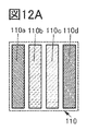
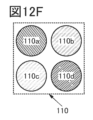
- 12A to 12H are top views showing examples of pixels.
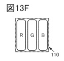
- 13A to 13J are top views showing examples of pixels.
- 14A to 14C are diagrams showing configuration examples of the touch sensor.
- FIG. 15 is a diagram illustrating a configuration example of a touch sensor and pixels.
- 16A and 16B are diagrams illustrating configuration examples of a touch sensor and pixels.
- FIG. 17 is a diagram illustrating a configuration example of a touch sensor and pixels.
- FIG. 18 is a diagram illustrating a configuration example of a touch sensor and pixels.
- FIG. 19 is a perspective view showing an example of a display device.
- FIG. 20 is a cross-sectional view showing an example of a display device.
- 21A and 21B are cross-sectional views showing an example of a display device.
- 22A and 22B are cross-sectional views showing an example of a display device.
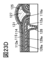
- 23A and 23B are cross-sectional views showing examples of transistors.
- 23C to 23E are cross-sectional views showing examples of display devices.
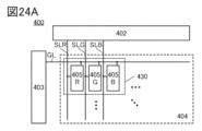
- FIG. 24A is a block diagram showing an example of a display device.
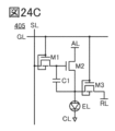
- 24B to 24D are diagrams showing examples of pixel circuits.
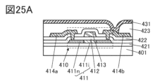
- 25A to 25D are diagrams illustrating examples of transistors.
- 26A and 26B are cross-sectional views showing an example of a display device.
- 27A and 27B are cross-sectional views showing examples of display devices.
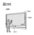
- 28A to 28F are diagrams illustrating examples of electronic devices.
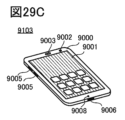
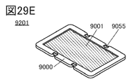
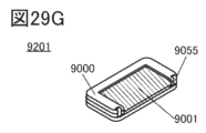
- 29A to 29G are diagrams illustrating examples of electronic devices.
- the display device may be read as an electronic device.
- a device manufactured using a metal mask or FMM may be referred to as a device with an MM (metal mask) structure.
- a device manufactured without using a metal mask or FMM may be referred to as a device with an MML (metal maskless) structure.
- holes or electrons are sometimes referred to as "carriers".
- the hole injection layer or electron injection layer is referred to as a "carrier injection layer”
- the hole transport layer or electron transport layer is referred to as a “carrier transport layer”
- the hole blocking layer or electron blocking layer is referred to as a "carrier It is sometimes called a block layer.
- the carrier injection layer, the carrier transport layer, and the carrier block layer described above may not be clearly distinguished from each other due to their cross-sectional shape, characteristics, or the like.
- one layer may serve as two or three functions of the carrier injection layer, the carrier transport layer, and the carrier block layer.
- One embodiment of the present invention is a display device having a display portion capable of full-color display.
- the display unit has first sub-pixels and second sub-pixels that emit different colors of light.
- the first subpixel has a first light emitting device that emits white light and the second subpixel also has a second light emitting device that emits white light.
- a first colored layer is provided to overlap the first light emitting device in the first subpixel, and a second colored layer is provided to overlap the second light emitting device in the second subpixel.
- the first colored layer and the second colored layer have different wavelength ranges of transmitted light. In this way, full-color display can be performed by using colored layers that transmit different colors of visible light for each sub-pixel.
- the light-emitting device used for each sub-pixel can be formed using the same material, the manufacturing process can be simplified and the manufacturing cost can be reduced. Note that in this specification and the like, sub-pixels are sometimes simply referred to as “pixels”.
- each sub-pixel is formed by a light-emitting device that emits white light, it is not necessary to separate the light-emitting layers in each sub-pixel. Therefore, a layer other than the pixel electrode included in the light-emitting device (for example, a light-emitting layer) can be shared by each sub-pixel.
- a layer other than the pixel electrode included in the light-emitting device for example, a light-emitting layer
- there are also layers with relatively high conductivity and when a layer with high conductivity is provided in common for each sub-pixel, leakage current may occur between the sub-pixels. .
- the display device has a high definition or a high aperture ratio and the distance between pixels becomes small, the leak current becomes a magnitude that cannot be ignored. As a result, the display quality is degraded due to a decrease in luminance, a decrease in contrast, and the like.
- power efficiency, power consumption, etc. deteriorate due to leakage current.
- a light-emitting device in which at least a portion is processed into an island shape by photolithography is used in each sub-pixel.
- the island-shaped portion of the light-emitting device includes a layer containing a light-emitting compound (also referred to as a light-emitting layer) included in the light-emitting device.
- a light-emitting compound also referred to as a light-emitting layer
- an island shape indicates a state in which two or more layers using the same material formed in the same step are physically separated.
- an island-shaped light-emitting layer means that the light-emitting layer is physically separated from an adjacent light-emitting layer.
- a layer including a light-emitting layer (which can be called an EL layer or part of the EL layer) is formed over one surface, and then a mask layer is formed over the EL layer. Then, a resist mask is formed over the mask layer, and the EL layer and the mask layer are processed using the resist mask to form an island-shaped EL layer used for each sub-pixel.
- each mask layer is positioned above at least the light-emitting layer (more specifically, among the layers constituting the EL layer, the layer processed into an island shape), Inside, it has a function of protecting the light-emitting layer.
- the mask layer may be referred to as a sacrificial layer.
- a structure in which a resist mask is formed directly above the light-emitting layer and processed using a photolithography method is conceivable.
- the light-emitting layer may be damaged (damage due to processing (for example, an etching process)), and the reliability may be significantly impaired. Therefore, when a display device of one embodiment of the present invention is manufactured, a functional layer (for example, a carrier block layer, a carrier transport layer, or a carrier injection layer, more specifically a hole block layer) located above the light emitting layer is used. It is preferable to use a method of forming a mask layer or the like on the layer, electron transport layer, or electron injection layer, and processing the light-emitting layer into an island shape. By applying the method, a highly reliable display device can be provided.
- the island-shaped EL layer manufactured by the method for manufacturing a display device of one embodiment of the present invention is not formed using a metal mask having a fine pattern, but the EL layer is formed over the entire surface. It is formed by processing after Therefore, it is possible to realize a high-definition display device or a display device with a high aperture ratio, which has hitherto been difficult to achieve. Furthermore, since the EL layer can be formed separately for each sub-pixel, a display device with extremely vivid, high-contrast, and high-quality display can be realized. Further, by providing the mask layer over the EL layer, damage to the EL layer during the manufacturing process of the display device can be reduced, and the reliability of the light-emitting device can be improved.
- the spacing between adjacent light emitting devices, the spacing between adjacent EL layers, or the spacing between adjacent pixel electrodes is less than 10 ⁇ m, 8 ⁇ m or less, 5 ⁇ m or less, 3 ⁇ m or less, 2 ⁇ m or less, 1.5 ⁇ m or less, 1 ⁇ m or less, or It can be narrowed down to 0.5 ⁇ m or less.
- the interval between adjacent light emitting devices, the interval between adjacent EL layers, or the interval between adjacent pixel electrodes can be reduced to, for example, 500 nm or less, 200 nm or less. Below, it can be narrowed to 100 nm or less, and further to 50 nm or less. As a result, the area of the non-light-emitting region that can exist between the two light-emitting devices can be greatly reduced, and the aperture ratio can be brought close to 100%.
- the aperture ratio is 40% or more, 50% or more, 60% or more, 70% or more, 80% or more, further 90% or more and less than 100%. It can also be realized.
- the reliability of the display device can be improved by increasing the aperture ratio of the display device. More specifically, when the lifetime of a display device using an organic EL device and having an aperture ratio of 10% is used as a reference, the life of the display device has an aperture ratio of 20% (that is, the aperture ratio is twice the reference). The life is about 3.25 times longer, and the life of a display device with an aperture ratio of 40% (that is, the aperture ratio is four times the reference) is about 10.6 times longer. As described above, the current density flowing through the organic EL device can be reduced as the aperture ratio is improved, so that the life of the display device can be extended. Since the aperture ratio of the display device of one embodiment of the present invention can be improved, the display quality of the display device can be improved. Further, as the aperture ratio of the display device is improved, the reliability (especially life) of the display device is significantly improved, which is an excellent effect.
- a layer located below the light-emitting layer (for example, a carrier injection layer or a carrier transport layer, more specifically a hole injection layer, a hole transport layer, etc.) ) is preferably processed into islands in the same pattern as the light-emitting layer.
- a layer located below the light-emitting layer is preferably processed into islands in the same pattern as the light-emitting layer.
- leakage current lateral leakage current, lateral leakage current, or lateral leakage current
- lateral leakage current may occur due to the hole injection layer.
- the hole-injection layer can be processed into an island shape in the same pattern as the light-emitting layer; therefore, lateral leakage current substantially occurs between adjacent subpixels. or the lateral leak current can be made extremely small.
- the pattern of the EL layer itself (which can be said to be a processing size) can also be made much smaller than when a metal mask is used.
- the thickness of the EL layer varies between the center and the edge, so the effective area that can be used as the light emitting region is smaller than the area of the EL layer. Become.
- the manufacturing method described above since a film having a uniform thickness is processed, an island-shaped EL layer can be formed with a uniform thickness. Therefore, almost the entire area of even a fine pattern can be used as a light emitting region. Therefore, a display device having both high definition and high aperture ratio can be manufactured.
- a layer including a light-emitting layer (which can be referred to as an EL layer or part of the EL layer) is formed over one surface
- a mask layer is formed over the EL layer. preferably formed. Then, it is preferable to form an island-shaped EL layer by forming a resist mask over the mask layer and processing the EL layer and the mask layer using the resist mask.
- the EL layer includes at least a light-emitting layer, and preferably consists of a plurality of layers. Specifically, it is preferable to have one or more layers on the light-emitting layer.
- the first layer and the second layer are each the light emitting layer and the carrier blocking layer (hole blocking layer or electron blocking layer) or carrier transporting layer (electron transporting layer or hole transporting layer) on the light emitting layer. ) and preferably.
- the layers included in the EL layer include a light emitting layer, a carrier injection layer (hole injection layer and electron injection layer), a carrier transport layer (hole transport layer and electron transport layer), and a carrier block layer (hole block layer and electron block layer).
- a common electrode which can also be called an upper electrode
- a carrier injection layer and a common electrode can be formed in common for each sub-pixel.
- the carrier injection layer is often a layer with relatively high conductivity among the EL layers. Therefore, the light-emitting device may be short-circuited when the carrier injection layer comes into contact with the side surface of a part of the EL layer formed like an island or the side surface of the pixel electrode. Note that even in the case where the carrier injection layer is provided in an island shape and the common electrode is formed in common for each sub-pixel, the common electrode and the side surface of the EL layer or the side surface of the pixel electrode are in contact with each other, so that light is emitted. The device may short out.
- the display device of one embodiment of the present invention includes an insulating layer covering at least the side surface of the island-shaped light-emitting layer.
- the side surface of the island-shaped light-emitting layer as used herein refers to a surface of the interface between the island-shaped light-emitting layer and another layer that is not parallel to the substrate (or the surface on which the light-emitting layer is formed). Also, it is not necessarily a mathematically exact plane or curved surface.
- the insulating layer preferably functions as a barrier insulating layer against at least one of water and oxygen. Further, the insulating layer preferably has a function of suppressing diffusion of at least one of water and oxygen. In addition, the insulating layer preferably has a function of capturing or fixing at least one of water and oxygen (also referred to as gettering).
- a barrier insulating layer indicates an insulating layer having barrier properties.
- barrier property refers to a function of suppressing diffusion of a corresponding substance (also referred to as low permeability).
- the corresponding substance has a function of capturing or fixing (also called gettering).
- an insulating layer having a function as a barrier insulating layer or a gettering function it is possible to suppress entry of impurities (typically, at least one of water and oxygen) that can diffuse into each light-emitting device from the outside. possible configuration. With such a structure, a highly reliable light-emitting device and a highly reliable display device can be provided.
- impurities typically, at least one of water and oxygen
- a display device of one embodiment of the present invention includes a pixel electrode functioning as an anode, and an island-shaped hole-injection layer, a hole-transport layer, a light-emitting layer, and a hole block provided in this order over the pixel electrode.
- a layer, an electron transport layer, an insulating layer provided to cover each side surface of the hole injection layer, the hole transport layer, the light emitting layer, the hole blocking layer, and the electron transport layer, and the electron transport layer It has an electron injection layer provided thereon and a common electrode provided on the electron injection layer and functioning as a cathode.
- a display device of one embodiment of the present invention includes a pixel electrode functioning as a cathode, and an island-shaped electron-injection layer, an electron-transport layer, a light-emitting layer, and an electron-blocking layer provided in this order over the pixel electrode. , and a hole transport layer, an insulating layer provided to cover each side surface of the electron injection layer, the electron transport layer, the light emitting layer, the electron blocking layer, and the hole transport layer, and on the hole transport layer and a common electrode provided on the hole injection layer and functioning as an anode.
- a hole injection layer or an electron injection layer is often a layer with relatively high conductivity among EL layers.
- the side surfaces of these layers are covered with the insulating layer; therefore, contact with a common electrode or the like can be suppressed. Therefore, short-circuiting of the light-emitting device can be suppressed, and the reliability of the light-emitting device can be improved.
- the insulating layer covering the side surface of the island-shaped EL layer may have a single-layer structure or a laminated structure.
- the insulating layer can be used as a protective insulating layer for the EL layer. Thereby, the reliability of the display device can be improved.
- the first insulating layer is preferably formed using an inorganic insulating material because it is formed in contact with the EL layer.
- an atomic layer deposition (ALD) method which causes less film damage.
- the inorganic insulating layer is formed using a sputtering method, a chemical vapor deposition (CVD) method, or a plasma enhanced CVD (PECVD) method, which has a higher film formation rate than the ALD method. preferably formed. Accordingly, a highly reliable display device can be manufactured with high productivity.
- the second insulating layer is preferably formed using an organic material so as to planarize the concave portion formed in the first insulating layer.
- an aluminum oxide film formed by an ALD method can be used as the first insulating layer, and an organic resin film can be used as the second insulating layer.
- the organic solvent contained in the organic resin film may damage the EL layer.
- an inorganic insulating film such as an aluminum oxide film formed by an ALD method as the first insulating layer, the organic resin film and the side surface of the EL layer are not in direct contact with each other. This can prevent the EL layer from being dissolved by the organic solvent.
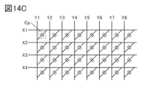
- the display device of one embodiment of the present invention includes a touch sensor that acquires position information of an object that touches or approaches the display surface.
- a touch sensor various systems such as a resistive film system, a capacitance system, an infrared system, an electromagnetic induction system, and a surface acoustic wave system can be adopted.
- a capacitive touch sensor it is preferable to use as the touch sensor.
- the capacitance method includes the surface-type capacitance method and the projection-type capacitance method. Also, the projective capacitance method includes a self-capacitance method, a mutual capacitance method, and the like. It is preferable to use the mutual capacitance method because it enables simultaneous multi-point detection.
- a mutual-capacitance touch sensor can be configured to have a plurality of electrodes to which a pulse potential is applied and a plurality of electrodes to which detection circuits are connected.
- a touch sensor can perform detection using a change in capacitance between electrodes when a finger or the like approaches. It is preferable that the electrodes constituting the touch sensor be arranged closer to the display surface than the light emitting device.
- At least part of the electrode of the touch sensor overlaps the region sandwiched between two adjacent light-emitting devices or the region sandwiched between two adjacent EL layers. Furthermore, it is preferable that at least part of the electrodes of the touch sensor have a region overlapping with an organic resin film provided between two adjacent EL layers. With such a structure, the touch sensor can be provided above the display device without reducing the light emitting area of the light emitting device. Therefore, a display device having both a high aperture ratio and high definition can be provided.
- a metal or alloy material as the conductive layer that functions as the electrode of the touch sensor.
- a non-light-transmitting metal or alloy material can be used for the electrodes of the touch sensor without reducing the aperture ratio of the display device. Touch sensing with high sensitivity can be achieved by using a metal or alloy material with low resistance for the electrodes of the touch sensor.
- a light-transmitting electrode that transmits light emitted by the light-emitting element can be used as the electrode of the touch sensor. At this time, the light-transmitting electrode can be provided so as to overlap with the light-emitting device.
- a light-emitting device can be provided between a pair of substrates.
- a rigid substrate such as a glass substrate may be used, or a flexible film may be used.
- the electrodes of the touch sensor can be formed on the substrate positioned on the display surface side.
- the electrodes of the touch sensor may be formed on another substrate and attached to the display surface side.
- the electrodes of the touch sensor between the pair of substrates.
- a structure in which a protective layer covering the light-emitting device is provided and electrodes of the touch sensor are provided over the protective layer can be employed.
- the number of parts can be reduced, and the manufacturing process can be simplified.
- the display device is particularly suitable for use as a flexible display using a flexible film as a substrate.
- [Configuration example 1 of display device] 1 to 10 show a display device of one embodiment of the present invention.
- FIG. 1A shows a top view of the display device 100.
- the display device 100 has a display section in which a plurality of pixels 110 are arranged, and a connection section 140 outside the display section. A plurality of sub-pixels are arranged in a matrix in the display section.
- FIG. 1A shows sub-pixels of 2 rows and 6 columns, which constitute pixels of 2 rows and 2 columns.
- the connection portion 140 can also be called a cathode contact portion.
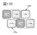
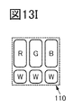
- a stripe arrangement is applied to the pixels 110 shown in FIG. 1A.
- the pixel 110 shown in FIG. 1A is composed of three sub-pixels, sub-pixels 110a, 110b, and 110c.
- the sub-pixels 110a, 110b, 110c each have a light emitting device that emits white light.
- a colored layer 132a, a colored layer 132b, or a colored layer 132c (hereinafter collectively referred to as a colored layer 132 in some cases) overlaps the light-emitting device. is provided.
- the sub-pixels 110a, 110b, and 110c emit light of different colors.
- the sub-pixels 110a, 110b, and 110c include three sub-pixels of red (R), green (G), and blue (B), and three sub-pixels of yellow (Y), cyan (C), and magenta (M). Color sub-pixels and the like are included. Also, the number of types of sub-pixels is not limited to three, and may be four or more.
- the four sub-pixels include R, G, B, and white (W) sub-pixels and R, G, B, and Y sub-pixels.
- the row direction is sometimes called the X direction
- the column direction is sometimes called the Y direction.
- the X and Y directions intersect, for example perpendicularly (see FIG. 1A).
- FIG. 1A shows an example in which sub-pixels of different colors are arranged side by side in the X direction and sub-pixels of the same color are arranged side by side in the Y direction.
- FIG. 1A shows an example in which the connecting portion 140 is positioned below the display portion when viewed from the top
- the connecting portion 140 may be provided at least one of the upper side, the right side, the left side, and the lower side of the display portion when viewed from above, and may be provided so as to surround the four sides of the display portion.
- the shape of the upper surface of the connecting portion 140 may be strip-shaped, L-shaped, U-shaped, frame-shaped, or the like.
- the number of connection parts 140 may be singular or plural.
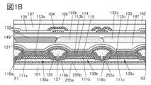
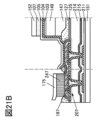
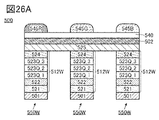
- FIG. 1B and 6C show cross-sectional views between the dashed-dotted line X1-X2 in FIG. 1A.
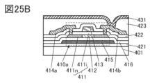
- a layer including a transistor is provided on the substrate 101, insulating layers 255a, 255b, and 255c are provided on the layer including the transistor, and the light emitting device 130a, 130b and 130c are provided, and a protective layer 131 is provided to cover these light emitting devices.
- An insulating layer 125 and an insulating layer 127 on the insulating layer 125 are provided in a region between adjacent light emitting devices. Note that the light emitting devices 130a, 130b, and 130c may be collectively referred to as the light emitting device 130 below.
- the display device 100 can be configured to have one insulating layer 125 and one insulating layer 127, for example.
- the display device 100 may have a plurality of insulating layers 125 separated from each other, and may have a plurality of insulating layers 127 separated from each other.
- a resin layer 147 is provided on the protective layer 131, a colored layer 132 is provided on the resin layer 147, and a resin layer 149 is provided on the colored layer 132.
- the colored layer 132a is provided so as to overlap the light emitting device 130a
- the colored layer 132b is provided so as to overlap the light emitting device 130b
- the colored layer 132c is provided so as to overlap the light emitting device 130c.
- the display device 100 includes an insulating layer 103, a conductive layer 104, an insulating layer 105, a conductive layer 106, an adhesive layer 107, a substrate 102, and is provided.
- a conductive layer 106 is provided on the insulating layer 105 .
- the substrate 102 is attached to the substrate 101 via the adhesive layer 107 .
- the adhesive layer 107 contacts the conductive layer 106 , the insulating layer 105 and the substrate 102 .
- the conductive layer 104 and the conductive layer 106 function as electrodes of the touch sensor.
- a mutual capacitance method is used as a touch sensor method, for example, a pulse potential is applied to one of the conductive layers 104 and 106, and an analog-to-digital (A-D) conversion circuit, sense amplifier, or the like is applied to the other. A detection circuit or the like may be connected.
- a capacitance is formed between the conductive layers 104 and 106 .
- the capacitance changes (specifically, the capacitance decreases). This change in capacitance appears as a change in amplitude of a signal generated in one of the conductive layers 104 and 106 when a pulse potential is applied to the other. Thereby, contact and proximity of a finger or the like can be detected.
- one of the conductive layer 104 and the conductive layer 106 may function as both electrodes of the touch sensor, and the other may function as a connection portion of the electrode of the touch sensor.
- a portion is formed in which the conductive layer 104 and the conductive layer 106 are in contact with each other through an opening formed in the insulating layer 105 .
- the display device of one embodiment of the present invention is a top emission type in which light is emitted in a direction opposite to the substrate over which the light emitting device is formed.
- the present invention is not limited to this. ).
- a stacked structure in which a plurality of transistors are provided on the substrate and an insulating layer is provided to cover these transistors can be applied.
- An insulating layer over a transistor may have a single-layer structure or a stacked-layer structure.
- FIG. 1B and the like among insulating layers over a transistor, an insulating layer 255a, an insulating layer 255b over the insulating layer 255a, and an insulating layer 255c over the insulating layer 255b are shown. These insulating layers may have recesses between adjacent light emitting devices.
- FIG. 1B and the like show an example in which a concave portion is provided in the insulating layer 255c.
- Various inorganic insulating films such as an oxide insulating film, a nitride insulating film, an oxynitride insulating film, and a nitride oxide insulating film can be preferably used as the insulating layer 255a, the insulating layer 255b, and the insulating layer 255c, respectively.
- an oxide insulating film or an oxynitride insulating film such as a silicon oxide film, a silicon oxynitride film, or an aluminum oxide film is preferably used.
- a nitride insulating film or a nitride oxide insulating film such as a silicon nitride film or a silicon nitride oxide film is preferably used. More specifically, a silicon oxide film is preferably used for the insulating layers 255a and 255c, and a silicon nitride film is preferably used for the insulating layer 255b.
- the insulating layer 255b preferably functions as an etching protection film.
- oxynitride refers to a material whose composition contains more oxygen than nitrogen
- nitride oxide refers to a material whose composition contains more nitrogen than oxygen. point to the material.
- silicon oxynitride refers to a material whose composition contains more oxygen than nitrogen
- silicon nitride oxide refers to a material whose composition contains more nitrogen than oxygen. indicates
- a configuration example of a layer including a transistor on the substrate 101 will be described later in Embodiment Modes 4 and 5.
- the light-emitting devices 130a, 130b, and 130c it is preferable to use light-emitting devices such as OLEDs (Organic Light Emitting Diodes) or QLEDs (Quantum-dot Light Emitting Diodes).
- OLEDs Organic Light Emitting Diodes
- QLEDs Quadantum-dot Light Emitting Diodes
- the light-emitting substance included in the light-emitting device include a substance that emits fluorescence (fluorescent material), a substance that emits phosphorescence (phosphorescent material), and a substance that exhibits thermally activated delayed fluorescence (thermally activated delayed fluorescence: TADF) material. ) and the like.
- the light-emitting substance of the light-emitting device not only organic compounds but also inorganic compounds (such as quantum dot materials) can be used as the light-emitting substance of the light-emitting device.
- the TADF material a material in which a singlet excited state and a triplet excited state are in thermal equilibrium may be used. Since such a TADF material has a short luminous lifetime (excitation lifetime), it is possible to suppress a decrease in luminous efficiency in a high-luminance region of a light-emitting device.
- a light-emitting device has an EL layer between a pair of electrodes.
- the EL layer has at least a light-emitting layer.
- one of a pair of electrodes may be referred to as a pixel electrode and the other may be referred to as a common electrode.
- one electrode functions as an anode and the other electrode functions as a cathode.
- the case where the pixel electrode functions as an anode and the common electrode functions as a cathode may be taken as an example.
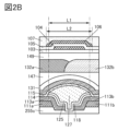
- Each end of the pixel electrode 111a, the pixel electrode 111b, and the pixel electrode 111c preferably has a tapered shape.
- the tapered shapes are also reflected in the first layer 113a, the second layer 113b, and the third layer 113c provided along the side surfaces of the pixel electrodes. .
- the side surface of the pixel electrode coverage of the EL layer provided along the side surface of the pixel electrode can be improved.
- the side surface of the pixel electrode is tapered because foreign matter (eg, dust or particles) in the manufacturing process can be easily removed by a treatment such as cleaning.
- the pixel electrodes 111a, 111b, and 111c may be collectively referred to as the pixel electrode 111 in some cases.
- the tapered shape refers to a shape in which at least a part of the side surface of the structure is inclined with respect to the substrate surface.
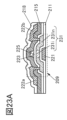
- the light-emitting device 130a includes the pixel electrode 111a on the insulating layer 255c, the island-shaped first layer 113a on the pixel electrode 111a, the common layer 114 on the island-shaped first layer 113a, and the common layer 114 on the common layer 114. and a common electrode 115 .
- the first layer 113a functions as an EL layer including a light-emitting layer.
- the first layer 113a and the common layer 114 can also be collectively called an EL layer.
- the light-emitting device 130b includes the pixel electrode 111b on the insulating layer 255c, the island-shaped second layer 113b on the pixel electrode 111b, the common layer 114 on the island-shaped second layer 113b, and the common layer 114 on the common layer 114. and a common electrode 115 .
- the second layer 113b functions as an EL layer including a light-emitting layer.
- the second layer 113b and the common layer 114 can also be collectively called an EL layer.
- the light-emitting device 130c includes the pixel electrode 111c on the insulating layer 255c, the island-shaped third layer 113c on the pixel electrode 111c, the common layer 114 on the island-shaped third layer 113c, and the common layer 114 on the common layer 114. and a common electrode 115 .
- the third layer 113c functions as an EL layer including a light-emitting layer.
- the third layer 113c and the common layer 114 can also be collectively called an EL layer.
- the first layer 113a, the second layer 113b, and the third layer 113c preferably emit white (W) light.
- the first layer 113a, the second layer 113b, and the third layer 113c are layers including at least a light-emitting layer.
- a colored layer 132a is provided to overlap the first layer 113a
- a colored layer 132b is provided to overlap the second layer 113b
- a colored layer 132c is provided to overlap the third layer 113c. Since the colored layers 132 transmit light in different wavelength ranges, the sub-pixels 110a, 110b, and 110c that emit light of different colors can be formed.
- the structure of the light-emitting device of this embodiment is not particularly limited, and may be a single structure or a tandem structure. A configuration example of the light emitting device will be described later.
- island-shaped layers provided for each light-emitting device are referred to as a first layer 113a, a second layer 113b, and a third layer 113c.
- a layer shared by the light emitting devices is shown as a common layer 114 .
- the first layer 113a, the second layer 113b, and the third layer 113c are processed into an island shape by photolithography. Therefore, each of the first layer 113a, the second layer 113b, and the third layer 113c forms an angle of approximately 90 degrees between the top surface and the side surface at the ends thereof.
- an organic film formed using FMM (Fine Metal Mask) or the like tends to gradually become thinner toward the edge. For example, since the upper surface is formed in a slope shape over a range of 1 ⁇ m or more and 10 ⁇ m or less in the vicinity of the end, the upper surface and the side surface are difficult to distinguish.
- the first layer 113a, the second layer 113b, and the third layer 113c are clearly distinguishable between the top surface and the side surface. Accordingly, in the adjacent first layer 113a and second layer 113b, one side surface of the first layer 113a and one side surface of the second layer 113b are arranged to face each other. Similarly, in the adjacent first layer 113a and third layer 113c, one side surface of the first layer 113a and one side surface of the third layer 113c are arranged to face each other. In the second layer 113b and the third layer 113c, one side surface of the second layer 113b and one side surface of the third layer 113c are arranged to face each other.
- first layer 113a, the second layer 113b, and the third layer 113c are processed into island shapes by a photolithography method, they can be separated from each other. Therefore, a current leakage path (leakage path) can be cut between adjacent EL layers, and leakage current can be suppressed. Accordingly, it is possible to improve luminance, contrast, display quality, power efficiency, power consumption, or the like in a light-emitting device.
- the first layer 113a, the second layer 113b, and the third layer 113c are respectively a hole injection layer, a hole transport layer, a hole blocking layer, a charge generation layer, an electron blocking layer, and an electron transport layer. , and an electron injection layer.
- the first layer 113a, the second layer 113b, and the third layer 113c may have a hole-injection layer, a hole-transport layer, a light-emitting layer, and an electron-transport layer.
- the first layer 113a, the second layer 113b, and the third layer 113c may have an electron injection layer, an electron transport layer, a light emitting layer, and a hole transport layer in this order. good. Further, a hole blocking layer may be provided between the electron transport layer and the light emitting layer. Also, a hole injection layer may be provided on the hole transport layer.
- the first layer 113a, the second layer 113b, and the third layer 113c preferably have a light-emitting layer and a carrier-transporting layer (electron-transporting layer or hole-transporting layer) on the light-emitting layer.
- the surfaces of the first layer 113a, the second layer 113b, and the third layer 113c are exposed during the manufacturing process of the display device. exposure to light can be suppressed, and damage to the light-emitting layer can be reduced. This can improve the reliability of the light emitting device.
- the first layer 113a, the second layer 113b, and the third layer 113c may have a structure including, for example, a first light-emitting unit, a charge generation layer, and a second light-emitting unit.
- the second light-emitting unit preferably has a light-emitting layer and a carrier-transporting layer (electron-transporting layer or hole-transporting layer) on the light-emitting layer. Since the surface of the second light-emitting unit is exposed during the manufacturing process of the display device, by providing the carrier transport layer on the light-emitting layer, the exposure of the light-emitting layer to the outermost surface is suppressed and damage to the light-emitting layer is prevented. can be reduced. This can improve the reliability of the light emitting device.
- the first layer 113a, the second layer 113b, and the third layer 113c should all be capable of emitting white light. Therefore, the first layer 113a, the second layer 113b, and the third layer 113c can have the same structure. Therefore, the first layer 113a, the second layer 113b, and the third layer 113c are formed by stacking films using the same material, and are formed into island-shaped third layers by photolithography. It can be processed into one layer 113a, an island-shaped second layer 113b, and an island-shaped third layer 113c. Thereby, the manufacturing process of the display device can be simplified, and the manufacturing cost can be reduced.
- the common layer 114 has, for example, an electron injection layer or a hole injection layer.
- the common layer 114 may have a laminate of an electron transport layer and an electron injection layer, or may have a laminate of a hole transport layer and a hole injection layer.
- Common layer 114 is shared by light emitting devices 130a, 130b, 130c.
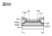
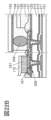
- the common electrode 115 is shared by the light emitting devices 130a, 130b, and 130c. As shown in FIGS. 6A and 6B, the common electrode 115 shared by the plurality of light emitting devices is electrically connected to the conductive layer 123 provided on the connection portion 140. As shown in FIGS. Here, FIGS. 6A and 6B are cross-sectional views along the dashed-dotted line Y1-Y2 in FIG. 1A. 6A and 6B do not show the structure above the protective layer 131, but the resin layer 147, the resin layer 149, the insulating layer 103, the conductive layer 104, the insulating layer 105, the conductive layer 106, and the adhesive layer 107. , and at least one of the substrate 102 can be provided as appropriate. For the conductive layer 123, a conductive layer formed using the same material and in the same process as the pixel electrode 111 is preferably used.
- FIG. 6A shows an example in which a common layer 114 is provided on the conductive layer 123 and the conductive layer 123 and the common electrode 115 are electrically connected through the common layer 114 .
- the common layer 114 may not be provided in the connecting portion 140 .
- conductive layer 123 and common electrode 115 are directly connected.
- a mask also referred to as an area mask or a rough metal mask to distinguish from a fine metal mask
- the common layer 114 and the common electrode 115 are formed into a region where a film is formed. can be changed.
- the protective layer 131 may have a single layer structure or a laminated structure of two or more layers.
- the conductivity of the protective layer 131 does not matter. At least one of an insulating film, a semiconductor film, and a conductive film can be used as the protective layer 131 .
- the protective layer 131 By including an inorganic film in the protective layer 131, deterioration of the light-emitting device is suppressed, such as prevention of oxidation of the common electrode 115 and entry of impurities (moisture, oxygen, etc.) into the light-emitting device. Reliability can be improved.
- inorganic insulating films such as oxide insulating films, nitride insulating films, oxynitride insulating films, and oxynitride insulating films can be used.
- oxide insulating films include silicon oxide films, aluminum oxide films, gallium oxide films, germanium oxide films, yttrium oxide films, zirconium oxide films, lanthanum oxide films, neodymium oxide films, hafnium oxide films, and tantalum oxide films.
- nitride insulating film include a silicon nitride film and an aluminum nitride film.
- the oxynitride insulating film examples include a silicon oxynitride film, an aluminum oxynitride film, and the like.
- the nitride oxide insulating film examples include a silicon nitride oxide film, an aluminum nitride oxide film, and the like.
- the protective layer 131 preferably includes a nitride insulating film or a nitride oxide insulating film, and more preferably includes a nitride insulating film.
- the protective layer 131 includes In—Sn oxide (also referred to as ITO), In—Zn oxide, Ga—Zn oxide, Al—Zn oxide, or indium gallium zinc oxide (In—Ga—Zn oxide).
- ITO In—Sn oxide
- In—Zn oxide Ga—Zn oxide
- Al—Zn oxide Al—Zn oxide
- indium gallium zinc oxide In—Ga—Zn oxide
- An inorganic film containing a material such as IGZO can also be used.
- the inorganic film preferably has a high resistance, and specifically, preferably has a higher resistance than the common electrode 115 .
- the inorganic film may further contain nitrogen.
- the protective layer 131 When the light emitted from the light-emitting device is taken out through the protective layer 131, the protective layer 131 preferably has high transparency to visible light.
- the protective layer 131 preferably has high transparency to visible light.
- ITO, IGZO, and aluminum oxide are preferable because they are inorganic materials with high transparency to visible light.
- the protective layer 131 for example, a stacked structure of an aluminum oxide film and a silicon nitride film over the aluminum oxide film, or a stacked structure of an aluminum oxide film and an IGZO film over the aluminum oxide film, or the like can be used. can be done. By using the stacked-layer structure, impurities (such as water and oxygen) entering the EL layer can be suppressed.
- the protective layer 131 may have an organic film.
- protective layer 131 may have both an organic film and an inorganic film.
- organic materials that can be used for the protective layer 131 include organic insulating materials that can be used for the insulating layer 121 described later.
- the protective layer 131 may have a two-layer structure formed using different film formation methods. Specifically, the first layer of the protective layer 131 may be formed using the ALD method, and the second layer of the protective layer 131 may be formed using the sputtering method.
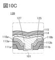
- no insulating layer is provided between the pixel electrode 111a and the first layer 113a to cover the edge of the upper surface of the pixel electrode 111a. Further, no insulating layer is provided between the pixel electrode 111b and the second layer 113b to cover the edge of the upper surface of the pixel electrode 111b. In addition, an insulating layer covering the upper surface edge of the pixel electrode 111c is not provided between the pixel electrode 111c and the third layer 113c. Therefore, the interval between adjacent light emitting devices can be made very narrow. Therefore, a high-definition or high-resolution display device can be obtained.
- the mask layer 118a is positioned on the first layer 113a of the light emitting device 130a, and the mask layer 118b is positioned on the second layer 113b of the light emitting device 130b.
- a mask layer 118c is located on the third layer 113c of the device 130c.
- the mask layer 118a is part of the remaining mask layer provided on the first layer 113a when the first layer 113a is processed.
- the mask layers 118b and 118c are part of the mask layers that were provided when the second layer 113b and the third layer 113c were formed, respectively.
- part of the mask layer used to protect the EL layer may remain during manufacturing.
- the same material may be used for any two or all of the mask layers 118a to 118c, or different materials may be used.
- the mask layer 118a, the mask layer 118b, and the mask layer 118c may be collectively called the mask layer 118 below.
- one edge of mask layer 118a is aligned or nearly aligned with an edge of first layer 113a, and the other edge of mask layer 118a is on top of first layer 113a.
- the other end of the mask layer 118a preferably overlaps with the first layer 113a and the pixel electrode 111a.
- the other end of the mask layer 118a is likely to be formed on the substantially flat surface of the first layer 113a.
- the mask layers 118b and 118c may remain, for example, between the island-shaped EL layer (the first layer 113a, the second layer 113b, or the third layer 113c) and the insulating layer 125. be.
- the mask layer 118 for example, one or more of a metal film, an alloy film, a metal oxide film, a semiconductor film, an organic insulating film, an inorganic insulating film, and the like can be used.
- various inorganic insulating films that can be used for the protective layer 131 can be used.
- inorganic insulating materials such as aluminum oxide, hafnium oxide, and silicon oxide can be used.
- the size relationship between the pixel electrode and the island-shaped EL layer is not particularly limited.
- the pixel electrode 111a and the first layer 113a will be described below as an example. The same applies to the pixel electrode 111b and the second layer 113b, and the pixel electrode 111c and the third layer 113c.
- FIG. 1B and the like show an example in which the end of the first layer 113a is located outside the end of the pixel electrode 111a.
- the first layer 113a is formed to cover the edge of the pixel electrode 111a.
- the aperture ratio can be increased compared to a structure in which the end portion of the island-shaped EL layer is located inside the end portion of the pixel electrode.
- the side surface of the pixel electrode with the EL layer, contact between the pixel electrode and the common electrode 115 (or the common layer 114) can be suppressed, so short-circuiting of the light emitting device can be suppressed. Also, the distance between the light emitting region of the EL layer (that is, the region overlapping with the pixel electrode) and the edge of the EL layer can be increased.
- An edge portion of the first layer 113a, an edge portion of the second layer 113b, and an edge portion of the third layer 113c include portions that may be damaged during the manufacturing process of the display device. By not using the portion as a light-emitting region, variation in characteristics of the light-emitting device can be suppressed, and reliability can be improved.
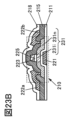
- the side surfaces of the first layer 113a, the second layer 113b, and the third layer 113c are covered with an insulating layer 127 and an insulating layer 125, respectively.
- a part of the upper surface of each of the first layer 113a, the second layer 113b, and the third layer 113c is covered with an insulating layer 127, an insulating layer 125, and a mask layer 118.
- the insulating layer 125 preferably covers at least one side surface of the island-shaped EL layer, and more preferably covers both side surfaces of the island-shaped EL layer.
- the insulating layer 125 can be in contact with each side surface of the island-shaped EL layer.
- FIG. 1B and the like show a configuration in which the end of the pixel electrode 111a is covered with the first layer 113a, and the insulating layer 125 is in contact with the side surface of the first layer 113a.
- the edge of the pixel electrode 111b is covered with the second layer 113b
- the edge of the pixel electrode 111c is covered with the third layer 113c
- the insulating layer 125 is formed on the side surface of the second layer 113b. and the side surface of the third layer 113c.
- the common layer 114 (or the common electrode 115) overlaps the side surfaces of the pixel electrodes 111a, 111b, and 111c, the first layer 113a, the second layer 113b, and the third layer 113c. Contact can be suppressed, and short circuit of the light emitting device can be suppressed. This can improve the reliability of the light emitting device.
- the insulating layer 127 is provided on the insulating layer 125 so as to fill the recesses of the insulating layer 125 .
- the insulating layer 127 overlaps with part of the top surface and the side surface of each of the first layer 113a, the second layer 113b, and the third layer 113c with the insulating layer 125 interposed therebetween (it can also be said to cover the side surface).
- the insulating layer 125 and the insulating layer 127 By providing the insulating layer 125 and the insulating layer 127, a space between adjacent island-shaped layers can be filled; It is possible to reduce unevenness with a large height difference on the formation surface and make it more flat. Therefore, the coverage of the carrier injection layer, the common electrode, and the like can be improved, and the disconnection of the carrier injection layer, the common electrode, and the like can be prevented.
- the common layer 114 and the common electrode 115 are provided on the first layer 113a, the second layer 113b, the third layer 113c, the mask layer 118, the insulating layer 125 and the insulating layer 127.
- a step is caused between a region where the pixel electrode and the EL layer are provided and a region where the pixel electrode and the EL layer are not provided (a region between the light emitting devices). ing. Since the display panel of one embodiment of the present invention includes the insulating layer 125 and the insulating layer 127 , the step can be planarized, and coverage with the common layer 114 and the common electrode 115 can be improved. Therefore, it is possible to suppress poor connection due to disconnection. In addition, it is possible to prevent the common electrode 115 from being locally thinned due to the steps and increasing the electrical resistance.
- the upper surface of the insulating layer 127 preferably has a more flat shape, but may have a convex portion, a convex curved surface, a concave curved surface, or a concave portion.
- the upper surface of the insulating layer 127 preferably has a highly flat and smooth convex shape.
- the insulating layer 125 can be provided so as to be in contact with the island-shaped EL layer. As a result, peeling of the island-shaped EL layer can be prevented. Adhesion between the insulating layer and the EL layer has the effect of fixing or bonding adjacent island-shaped EL layers to each other by the insulating layer. This can improve the reliability of the light emitting device. Moreover, the production yield of the light-emitting device can be increased.
- the insulating layer 125 has a region in contact with the side surface of the island-shaped EL layer and functions as a protective insulating layer for the EL layer.
- impurities oxygen, moisture, and the like
- the display panel can have high reliability.
- the insulating layer 125 can be an insulating layer having an inorganic material.
- an inorganic insulating film such as an oxide insulating film, a nitride insulating film, an oxynitride insulating film, or a nitride oxide insulating film can be used, for example.
- the insulating layer 125 may have a single-layer structure or a laminated structure.
- the oxide insulating film includes a silicon oxide film, an aluminum oxide film, a magnesium oxide film, an indium gallium zinc oxide film, a gallium oxide film, a germanium oxide film, an yttrium oxide film, a zirconium oxide film, a lanthanum oxide film, a neodymium oxide film, and an oxide film.
- a hafnium film, a tantalum oxide film, and the like are included.
- the nitride insulating film include a silicon nitride film and an aluminum nitride film.
- Examples of the oxynitride insulating film include a silicon oxynitride film, an aluminum oxynitride film, and the like.
- the nitride oxide insulating film examples include a silicon nitride oxide film, an aluminum nitride oxide film, and the like.
- aluminum oxide is preferable because it has a high etching selectivity with respect to the EL layer and has a function of protecting the EL layer during formation of the insulating layer 127 described later.
- an inorganic insulating film such as an aluminum oxide film, a hafnium oxide film, or a silicon oxide film formed by an ALD method to the insulating layer 125, the insulating layer 125 has few pinholes and has an excellent function of protecting the EL layer. can be formed.
- the insulating layer 125 may have a layered structure of a film formed by an ALD method and a film formed by a sputtering method.
- the insulating layer 125 may have a laminated structure of, for example, an aluminum oxide film formed by ALD and a silicon nitride film formed by sputtering.
- the insulating layer 125 preferably functions as a barrier insulating layer against at least one of water and oxygen. Further, the insulating layer 125 preferably has a function of suppressing diffusion of at least one of water and oxygen. Further, the insulating layer 125 preferably has a function of capturing or fixing at least one of water and oxygen (also referred to as gettering).
- the insulating layer 125 has a function as a barrier insulating layer or a gettering function to suppress entry of impurities (typically, at least one of water and oxygen) that can diffuse into each light-emitting device from the outside. is possible. With such a structure, a highly reliable light-emitting device and a highly reliable display panel can be provided.
- impurities typically, at least one of water and oxygen
- the insulating layer 125 preferably has a low impurity concentration. Accordingly, it is possible to suppress deterioration of the EL layer due to entry of impurities from the insulating layer 125 into the EL layer. In addition, by reducing the impurity concentration in the insulating layer 125, the barrier property against at least one of water and oxygen can be improved.
- the insulating layer 125 preferably has a sufficiently low hydrogen concentration or carbon concentration, or preferably both.
- Methods for forming the insulating layer 125 include a sputtering method, a CVD method, a pulsed laser deposition (PLD) method, an ALD method, and the like.
- the insulating layer 125 is preferably formed by an ALD method with good coverage.
- the substrate temperature is preferably 60° C. or higher, more preferably 80° C. or higher, more preferably 100° C. or higher, and more preferably 120° C. or higher.
- the substrate temperature is preferably 200° C. or lower, more preferably 180° C. or lower, more preferably 160° C. or lower, more preferably 150° C. or lower, and more preferably 140° C. or lower.
- heat resistant temperature indicators include glass transition point, softening point, melting point, thermal decomposition temperature, and 5% weight loss temperature.
- the heat resistance temperature of the EL layer can be any one of these temperatures, preferably the lowest temperature among them.
- the insulating layer 125 it is preferable to form an insulating film having a thickness of, for example, 3 nm or more, 5 nm or more, or 10 nm or more and 200 nm or less, 150 nm or less, 100 nm or less, or 50 nm or less.
- the insulating layer 127 provided on the insulating layer 125 has a function of flattening unevenness with a large height difference of the insulating layer 125 formed between adjacent light emitting devices. In other words, the presence of the insulating layer 127 has the effect of improving the flatness of the surface on which the common electrode 115 is formed.
- An insulating layer containing an organic material can be suitably used as the insulating layer 127 .
- the organic material it is preferable to use a photosensitive organic resin, and for example, a photosensitive resin composition containing an acrylic resin may be used.
- the viscosity of the material of the insulating layer 127 may be 1 cP or more and 1500 cP or less, preferably 1 cP or more and 12 cP or less. By setting the viscosity of the material of the insulating layer 127 within the above range, the insulating layer 127 having a tapered shape, which will be described later, can be formed relatively easily.
- acrylic resin does not only refer to polymethacrylate esters or methacrylic resins, but may refer to all acrylic polymers in a broad sense.
- the insulating layer 127 only needs to have a tapered side surface as described later, and the organic material that can be used as the insulating layer 127 is not limited to the above.
- acrylic resin, polyimide resin, epoxy resin, imide resin, polyamide resin, polyimideamide resin, silicone resin, siloxane resin, benzocyclobutene-based resin, phenolic resin, and precursors of these resins are applied. sometimes you can.
- an organic material such as polyvinyl alcohol (PVA), polyvinyl butyral, polyvinylpyrrolidone, polyethylene glycol, polyglycerin, pullulan, water-soluble cellulose, or alcohol-soluble polyamide resin can be used in some cases.
- PVA polyvinyl alcohol
- polyvinyl butyral polyvinylpyrrolidone
- polyethylene glycol polyglycerin
- pullulan polyethylene glycol
- polyglycerin polyglycerin
- pullulan polyethylene glycol
- pullulan polyglycerin
- pullulan water-soluble cellulose
- alcohol-soluble polyamide resin water-soluble polyamide resin
- a photoresist can be used as the photosensitive resin in some cases.
- a positive material or a negative material can be used as the photosensitive resin in some cases.
- a material that absorbs visible light may be used for the insulating layer 127 . Since the insulating layer 127 absorbs light emitted from the light emitting device, leakage of light (stray light) from the light emitting device to an adjacent light emitting device via the insulating layer 127 can be suppressed. Thereby, the display quality of the display panel can be improved. In addition, since the display quality can be improved without using a polarizing plate for the display panel, the weight and thickness of the display panel can be reduced.
- Materials that absorb visible light include materials containing pigments such as black, materials containing dyes, light-absorbing resin materials (e.g., polyimide), and resin materials that can be used for color filters (color filter materials ).
- resin materials that can be used for color filters color filter materials
- by mixing color filter materials of three or more colors it is possible to obtain a black or nearly black resin layer.
- the insulating layer 127 is formed using a wet film formation method such as spin coating, dipping, spray coating, inkjet, dispensing, screen printing, offset printing, doctor knife method, slit coating, roll coating, curtain coating, knife coating, or the like. can be formed. In particular, it is preferable to form the insulating layer 127 by spin coating.
- the insulating layer 127 is formed at a temperature lower than the heat-resistant temperature of the EL layer.
- the substrate temperature when forming the insulating layer 127 is typically 200° C. or lower, preferably 180° C. or lower, more preferably 160° C. or lower, more preferably 150° C. or lower, and more preferably 140° C. or lower. .
- the structure of the insulating layer 127 and the like will be described below, taking the structure of the insulating layer 127 between the light emitting device 130a and the light emitting device 130b as an example. The same applies to the insulating layer 127 between the light emitting device 130b and the light emitting device 130c, the insulating layer 127 between the light emitting device 130c and the light emitting device 130a, and the like. In the following description, an end portion of the insulating layer 127 over the second layer 113b may be taken as an example. The same can be said for the edge of the upper insulating layer 127 and the like.
- the insulating layer 127 preferably has a tapered shape with a taper angle ⁇ 1 on the side surface in a cross-sectional view of the display device.
- the taper angle ⁇ 1 is the angle between the side surface of the insulating layer 127 and the substrate surface.
- the angle formed by the side surface of the insulating layer 127 with the upper surface of the flat portion of the insulating layer 125, the upper surface of the flat portion of the second layer 113b, or the upper surface of the flat portion of the pixel electrode 111b is not limited to the substrate surface. good.
- the side surface of the insulating layer 127 is a convex curved surface above the flat portion of the first layer 113a, the second layer 113b, or the third layer 113c, as shown in FIG. 1B. Sometimes refers to the side of the shape part. Further, when the side surface of the insulating layer 127 is tapered, the side surface of the insulating layer 125 and the side surface of the mask layer 118 may also be tapered.
- the taper angle ⁇ 1 of the insulating layer 127 is less than 90°, preferably 60° or less, more preferably 45° or less.
- the upper surface of the insulating layer 127 preferably has a convex shape.
- the convex curved surface shape of the upper surface of the insulating layer 127 is preferably a shape that gently swells toward the center. Further, it is preferable that the convex curved surface portion at the center of the upper surface of the insulating layer 127 has a shape that is smoothly connected to the tapered portion at the end of the side surface.
- the insulating layer 127 is formed in a region between two EL layers (for example, a region between the first layer 113a and the second layer 113b). At this time, at least part of the insulating layer 127 is formed on the side edge of one EL layer (eg, the first layer 113a) and the side edge of the other EL layer (eg, the second layer 113b). It will be placed in a sandwiched position.
- one end of the insulating layer 127 overlaps with the pixel electrode 111a and the other end of the insulating layer 127 overlaps with the pixel electrode 111b.
- the end portion of the insulating layer 127 can be formed on the substantially flat region of the first layer 113a (second layer 113b). Therefore, it becomes relatively easy to process the tapered shape of the insulating layer 127 as described above.
- the display quality of the display device according to one embodiment of the present invention can be improved.
- the display device of this embodiment can reduce the distance between the light emitting devices.
- the distance between light-emitting devices, the distance between EL layers, or the distance between pixel electrodes is less than 10 ⁇ m, 8 ⁇ m or less, 5 ⁇ m or less, 3 ⁇ m or less, 2 ⁇ m or less, 1 ⁇ m or less, 500 nm or less, 200 nm or less, or 100 nm or less.
- the display device of this embodiment has a region where the distance between two adjacent island-shaped EL layers is 1 ⁇ m or less, preferably 0.5 ⁇ m (500 nm) or less, more preferably 0.5 ⁇ m (500 nm) or less. has a region of 100 nm or less.
- one end of the insulating layer 127 overlaps with the pixel electrode 111a and the other end of the insulating layer 127 overlaps with the pixel electrode 111b, but the present invention is not limited to this. .
- the insulating layer 127 may not overlap with the pixel electrodes 111a and 111b.
- FIG. 1B and the like show a configuration in which the edge of the insulating layer 127 substantially matches the edge of the mask layer 118 and the edge of the insulating layer 125
- the present invention is not limited to this.
- the end of the insulating layer 127 may be positioned outside the end of the mask layer 118 and the end of the insulating layer 125 .
- the edge of the mask layer 118 and the edge of the insulating layer 125 may be covered with the insulating layer 127 .
- the end portion of the insulating layer 127 can be smoothly connected to the top surface of the EL layer, and the common layer 114 and the common electrode 115 provided over the insulating layer 127 can be easily covered.
- a colored layer 132a, a colored layer 132b, and a colored layer 132c are provided between the common electrode 115 and the insulating layer 105, in other words, between the light emitting device and the touch sensor. can do.
- the distance between the light emitting device 130 and the colored layer 132 can be shortened. Therefore, it is possible to suppress leakage of light emitted from the light emitting device 130 to adjacent sub-pixels.
- light emitted from the light emitting device 130a overlapping the colored layer 132a can be prevented from entering the colored layer 132b.
- the contrast of the image displayed on the display device can be increased, and the display device with high display quality can be realized.
- the colored layer 132a has a region overlapping with the light emitting device 130a
- the colored layer 132b has a region overlapping with the light emitting device 130b
- the colored layer 132c has a region overlapping with the light emitting device 130c.
- the colored layer 132 a , the colored layer 132 b , and the colored layer 132 c have at least regions overlapping with the light-emitting layers of the respective light-emitting devices 130 .
- the colored layer 132a, the colored layer 132b, and the colored layer 132c have a function of transmitting light in wavelength ranges different from each other.
- the colored layer 132a has a function of transmitting light having an intensity in the red wavelength region
- the colored layer 132b has a function of transmitting light having an intensity in the green wavelength region
- the colored layer 132c has a function of transmitting blue light. It can be configured to have a function of transmitting light having intensity in the wavelength range. Accordingly, the display device 100 can perform full-color display.
- the colored layer 132 is not limited to this, and may have a function of transmitting any one of cyan, magenta, and yellow light.
- the adjacent colored layers 132 preferably have overlapping regions. Specifically, it is preferable to have a region where the adjacent colored layer 132 overlaps in a region that does not overlap with the light emitting device 130 .
- a colored layer 132a is provided overlying part of the colored layer 132b in a region sandwiched between the light emitting devices 130a and 130b. At this time, it is preferable that a portion where the colored layer 132 a and the colored layer 132 b overlap overlap with the insulating layer 127 .
- the colored layers 132 can function as a light shielding layer in the region where the colored layers 132 overlap. Therefore, the light emitted from the light emitting device 130 can be prevented from leaking to adjacent sub-pixels, thereby increasing the contrast of an image displayed on the display device, and realizing a display device with high display quality.
- the colored layer 132 is preferably provided in contact with the upper surface of the resin layer 147 that functions as a planarizing film. Accordingly, the colored layer 132 can be formed on a surface with high flatness, so that unevenness depending on the surface to be formed can be reduced in the colored layer 132 . Therefore, part of the light emitted from the light-emitting device 130 is less likely to be irregularly reflected by the unevenness of the colored layer 132, and the display quality of the display device can be improved. Further, by providing the resin layer 147 on the protective layer 131, even if the protective layer 131 has a defect such as a pinhole, the defect can be filled with the resin layer 147 having high step coverage.
- the resin layer 147 preferably contains an organic insulating material.
- organic insulating material examples include acrylic resins, polyimide resins, epoxy resins, polyamide resins, polyimideamide resins, siloxane resins, benzocyclobutene resins, phenolic resins, and precursors of these resins.
- FIGS. 2A and 2B are enlarged views of a region sandwiched between the first layer 113a and the second layer 113b shown in FIG. 1B. 2A and 2B and the like, the region sandwiched between the first layer 113a and the third layer 113c and the second layer, which are not illustrated in FIGS. The same applies to the region sandwiched between 113b and the third layer 113c.
- the conductive layer 104 is provided on the insulating layer 103 .
- An insulating layer 105 is provided to cover the conductive layer 104 and the insulating layer 103 .
- a conductive layer 106 is provided on the insulating layer 105 .
- the insulating layer 103 is provided on the resin layer 149 provided on the colored layer 132 .
- the conductive layer 106 and the insulating layer 105 are attached to the substrate 102 by an adhesive layer 107 .
- Either or both of the conductive layer 104 and the conductive layer 106 function as electrodes of the touch sensor.
- a touch sensor is configured by a conductive layer 104 and a conductive layer 106 formed with an insulating layer 105 interposed therebetween is shown.
- the thickness of the display device 100 can be made extremely thin.
- the conductive layer 104 and the conductive layer 106 are not provided on the substrate 102 side of the display device 100, the substrates 102 and 101 do not need to be attached with high accuracy, and the manufacturing yield can be increased.
- the substrate 102 may be a substrate having a light-transmitting property, and the degree of freedom in material selection is extremely high.
- FIG. 1B also shows a portion where the conductive layer 104 and the conductive layer 106 overlap. For example, it can be applied to a portion where the conductive layer 104 and the conductive layer 106 intersect. Also, the configuration of a connection portion where the conductive layer 104 and the conductive layer 106 are electrically connected is shown. At the connection portion, the conductive layer 104 and the conductive layer 106 are electrically connected through an opening provided in the insulating layer 105 . The connection portion can be applied to a portion where two island-shaped conductive layers 104 are electrically connected by the conductive layer 106, for example.
- the conductive layer 104 and the conductive layer 106 are provided to avoid the light emitting region of the light emitting device 130a and the light emitting region of the light emitting device 130b. In other words, the conductive layer 104 and the conductive layer 106 overlap with a region sandwiched between two adjacent light emitting devices or a region sandwiched between two adjacent EL layers.
- the conductive layers 104 and 106 have regions overlapping with the insulating layer 127 .
- the length L2 of the conductive layer 106 in the X1-X2 direction is smaller than the length L1 of the insulating layer 127 in the X1-X2 direction.
- the side surface of the conductive layer 104 and the side surface of the conductive layer 106 are preferably positioned inside the side surface of the insulating layer 127 (which can also be called an end portion of the insulating layer 127) in a cross-sectional view.
- the conductive layers 104 and 106 can be provided so as not to interfere with light emission of the light-emitting device. can be provided. Accordingly, a low-resistance conductive material such as a metal or an alloy can be used for the conductive layers 104 and 106 without using a light-transmitting conductive material, so that the sensitivity of the touch sensor can be increased. .
- the display device of one embodiment of the present invention can have both a high aperture ratio and high definition by using the MML structure. Furthermore, by providing the conductive layers 104 and 106 as described above, the touch sensor can be provided while maintaining a high aperture ratio.
- both the conductive layer 104 and the conductive layer 106 overlap the region sandwiched between two adjacent light emitting devices, but this is not the only option.
- Either the conductive layer 104 or the conductive layer 106 may overlap with a region sandwiched between two adjacent light-emitting devices or a region sandwiched between two adjacent EL layers.
- one of the conductive layers 104 and 106 may have a region overlapping with the insulating layer 127 .
- FIG. 2A shows a structure in which the length L2 of the conductive layer 106 in the X1-X2 direction is smaller than the length L1 of the insulating layer 127 in the X1-X2 direction, but the present invention is not limited to this. .
- the length L2 of the conductive layer 106 in the X1-X2 direction is larger than the length L1 of the insulating layer 127 in the X1-X2 direction.
- a structure that does not overlap with the insulating layer 127 can also be employed.
- regions of the conductive layers 104 and 106 which do not overlap with the insulating layer 127 are preferably small in order to prevent the aperture ratio of the display device from being reduced.
- a conductive film containing a metal or an alloy can be used as the conductive layer 104 and the conductive layer 106 .
- the conductive layer 104 and the conductive layer 106 for example, metals such as aluminum, titanium, chromium, nickel, copper, yttrium, zirconium, molybdenum, silver, tantalum, and tungsten, and alloys containing these metals as main components are used. membranes, and the like.
- a film containing these materials can be used as a single layer or as a laminated structure.
- An inorganic insulating film or an organic insulating film can be used as the insulating layer 105 .
- examples thereof include resins such as acrylic resins and epoxy resins, and inorganic insulating materials such as silicon oxide, silicon oxynitride, silicon nitride oxide, silicon nitride, and aluminum oxide.
- the insulating layer 105 may have a single layer structure or a laminated structure.
- the insulating layer 103 preferably contains an inorganic insulating material.
- examples include oxides or nitrides such as silicon oxide, silicon oxynitride, silicon nitride oxide, silicon nitride, aluminum oxide, aluminum oxynitride, and hafnium oxide.
- the resin layer 149 preferably contains an organic insulating material, like the resin layer 147 .
- organic insulating material like the resin layer 147 .
- examples thereof include acrylic resins, polyimide resins, epoxy resins, polyamide resins, polyimideamide resins, siloxane resins, benzocyclobutene resins, phenolic resins, and precursors of these resins.
- the insulating layer 103 By forming the insulating layer 103 on the upper surface of the resin layer 149 that functions as a planarizing film, an insulating film with few defects can be formed as the insulating layer 103 .
- an insulating film with few defects can be formed as the insulating layer 103 .
- it functions as an etching stopper when the conductive layer 104 is processed (etched), and can prevent the resin layer 149 from being scraped.
- FIG. 1B shows an example in which the insulating layer 103 is laminated on the resin layer 149
- the present invention is not limited to this.
- a configuration in which either one of the resin layer 149 and the insulating layer 103 is not provided can also be employed.
- various curable adhesives such as photocurable adhesives such as ultraviolet curable adhesives, reaction curable adhesives, thermosetting adhesives, and anaerobic adhesives can be used.
- These adhesives include epoxy resins, acrylic resins, silicone resins, phenol resins, polyimide resins, imide resins, PVC (polyvinyl chloride) resins, PVB (polyvinyl butyral) resins, EVA (ethylene vinyl acetate) resins, and the like.
- a material with low moisture permeability such as epoxy resin is preferable.
- a two-liquid mixed type resin may be used.
- an adhesive sheet or the like may be used.
- a light shielding layer may be provided on the surface of the substrate 102 on the adhesive layer 107 side.
- various optical members can be arranged outside the substrate 102 .
- optical members include polarizing plates, retardation plates, light diffusion layers (diffusion films, etc.), antireflection layers, light collecting films, and the like.
- an antistatic film that suppresses adhesion of dust, a water-repellent film that prevents adhesion of dirt, a hard coat film that suppresses the occurrence of scratches due to use, a shock absorption layer, etc. Layers may be arranged.
- a glass layer or a silica layer (SiO x layer) as a surface protective layer, because surface contamination and scratching can be suppressed.
- the surface protective layer DLC (diamond-like carbon), aluminum oxide (AlO x ), polyester-based material, polycarbonate-based material, or the like may be used.
- a material having a high visible light transmittance is preferably used for the surface protective layer.
- the substrates 101 and 102 glass, quartz, ceramics, sapphire, resins, metals, alloys, semiconductors, etc. can be used.
- a material that transmits the light is used for the substrate on the side from which the light from the light-emitting device is extracted.
- the flexibility of the display device can be increased.
- polarizing plates may be used as the substrates 101 and 102 .
- polyester resins such as polyethylene terephthalate (PET) and polyethylene naphthalate (PEN), polyacrylonitrile resins, acrylic resins, polyimide resins, polymethyl methacrylate resins, polycarbonate (PC) resins, and polyether resins are used, respectively.
- PES resin Sulfone (PES) resin, polyamide resin (nylon, aramid, etc.), polysiloxane resin, cycloolefin resin, polystyrene resin, polyamideimide resin, polyurethane resin, polyvinyl chloride resin, polyvinylidene chloride resin, polypropylene resin, polytetrafluoroethylene (PTFE) resin, ABS resin, cellulose nanofiber, or the like can be used.
- a flexible glass may be used for the substrates 101 and 102 .
- a substrate having high optical isotropy has small birefringence (it can be said that the amount of birefringence is small).
- the absolute value of the retardation (retardation) value of the substrate with high optical isotropy is preferably 30 nm or less, more preferably 20 nm or less, and even more preferably 10 nm or less.
- Films with high optical isotropy include triacetyl cellulose (TAC, also called cellulose triacetate) films, cycloolefin polymer (COP) films, cycloolefin copolymer (COC) films, and acrylic films.
- TAC triacetyl cellulose
- COP cycloolefin polymer
- COC cycloolefin copolymer
- the film when a film is used as the substrate, the film may absorb water, which may cause shape changes such as wrinkles in the display device. Therefore, it is preferable to use a film having a low water absorption rate as the substrate. For example, it is preferable to use a film with a water absorption of 1% or less, more preferably 0.1% or less, and even more preferably 0.01% or less.
- a conductive film that transmits visible light is used for the electrode on the light extraction side of the pixel electrode and common electrode.
- a conductive film that reflects visible light is preferably used for the electrode on the side from which light is not extracted.
- the display device has a light-emitting device that emits infrared light
- a conductive film that transmits visible light and infrared light is used for the electrode on the side from which light is extracted, and a conductive film is used for the electrode on the side that does not extract light.
- a conductive film that reflects visible light and infrared light is preferably used.
- a conductive film that transmits visible light may also be used for the electrode on the side from which light is not extracted.
- the electrode is preferably arranged between the reflective layer and the EL layer. That is, the light emitted from the EL layer may be reflected by the reflective layer and extracted from the display device.
- indium tin oxide In—Sn oxide, also referred to as ITO
- In—Si—Sn oxide also referred to as ITSO
- indium zinc oxide In—Zn oxide
- In—W -Zn oxide Indium tin oxide
- alloys containing aluminum such as alloys of aluminum, nickel, and lanthanum (Al-Ni-La), alloys of silver and magnesium, and alloys of silver, palladium and copper (Ag-Pd- Cu, also referred to as APC) and other silver-containing alloys.
- aluminum alloys such as alloys of aluminum, nickel, and lanthanum (Al-Ni-La), alloys of silver and magnesium, and alloys of silver, palladium and copper (Ag-Pd- Cu, also referred to as APC) and other silver-containing alloys.
- elements belonging to Group 1 or Group 2 of the periodic table of elements not exemplified above e.g., lithium (Li), cesium (Cs), calcium (Ca), strontium (Sr)), europium (Eu), ytterbium
- Yb rare earth metal
- an alloy containing an appropriate combination thereof, graphene, or the like can be used.
- a micro optical resonator (microcavity) structure is preferably applied to the light emitting device. Therefore, one of the pair of electrodes included in the light-emitting device is preferably an electrode (semi-transmissive/semi-reflective electrode) that is transparent and reflective to visible light, and the other is an electrode that is reflective to visible light ( reflective electrode). Since the light-emitting device has a microcavity structure, the light emitted from the light-emitting layer can be resonated between both electrodes, and the light emitted from the light-emitting device can be enhanced.
- the semi-transmissive/semi-reflective electrode can also have a laminated structure of a reflective electrode and an electrode having transparency to visible light (also referred to as a transparent electrode).
- the light transmittance of the transparent electrode is set to 40% or more.
- the light-emitting device preferably uses an electrode having a transmittance of 40% or more for visible light (light with a wavelength of 400 nm or more and less than 750 nm).
- the visible light reflectance of the semi-transmissive/semi-reflective electrode is 10% or more and 95% or less, preferably 30% or more and 80% or less.
- the visible light reflectance of the reflective electrode is 40% or more and 100% or less, preferably 70% or more and 100% or less.
- the resistivity of these electrodes is preferably 1 ⁇ 10 ⁇ 2 ⁇ cm or less.
- a light-emitting layer is a layer containing a light-emitting material (also called a light-emitting substance).
- the emissive layer can have one or more emissive materials.
- a substance exhibiting emission colors such as blue, purple, violet, green, yellow-green, yellow, orange, and red is used as appropriate.
- White light emission can be obtained from the light-emitting device 130 by forming the light-emitting layer by selecting these light-emitting substances so that they have a complementary color relationship. Note that a substance that emits near-infrared light can also be used as the light-emitting substance.
- Examples of light-emitting substances include fluorescent materials, phosphorescent materials, TADF materials, and quantum dot materials.
- fluorescent materials include pyrene derivatives, anthracene derivatives, triphenylene derivatives, fluorene derivatives, carbazole derivatives, dibenzothiophene derivatives, dibenzofuran derivatives, dibenzoquinoxaline derivatives, quinoxaline derivatives, pyridine derivatives, pyrimidine derivatives, phenanthrene derivatives, and naphthalene derivatives. be done.
- Examples of phosphorescent materials include organometallic complexes (especially iridium complexes) having a 4H-triazole skeleton, 1H-triazole skeleton, imidazole skeleton, pyrimidine skeleton, pyrazine skeleton, or pyridine skeleton, and phenylpyridine derivatives having an electron-withdrawing group.
- organometallic complexes especially iridium complexes
- platinum complexes, rare earth metal complexes, etc. which are used as ligands, can be mentioned.
- the light-emitting layer may contain one or more organic compounds (host material, assist material, etc.) in addition to the light-emitting substance (guest material).
- One or both of a hole-transporting material and an electron-transporting material can be used as the one or more organic compounds.
- Bipolar materials or TADF materials may also be used as one or more organic compounds.
- the light-emitting layer preferably includes, for example, a phosphorescent material and a combination of a hole-transporting material and an electron-transporting material that easily form an exciplex.
- ExTET Exciplex-Triplet Energy Transfer
- a combination that forms an exciplex exhibiting light emission at a wavelength that overlaps with the wavelength of the absorption band on the lowest energy side of the light-emitting substance energy transfer becomes smooth and light emission can be efficiently obtained. With this configuration, high efficiency, low-voltage driving, and long life of the light-emitting device can be realized at the same time.
- the first layer 113a, the second layer 113b, and the third layer 113c each include a substance with a high hole-injection property, a substance with a high hole-transport property, and a hole-blocking material as layers other than the light-emitting layer. , a substance with a high electron-transport property, a substance with a high electron-injection property, an electron-blocking material, a bipolar substance (a substance with high electron-transport property and hole-transport property), or the like.
- Both low-molecular-weight compounds and high-molecular-weight compounds can be used in the light-emitting device, and inorganic compounds may be included.
- Each of the layers constituting the light-emitting device can be formed by a vapor deposition method (including a vacuum vapor deposition method), a transfer method, a printing method, an inkjet method, a coating method, or the like.
- the first layer 113a, the second layer 113b, and the third layer 113c are respectively a hole-injecting layer, a hole-transporting layer, a hole-blocking layer, an electron-blocking layer, an electron-transporting layer, and an electron layer. It may have one or more of the injection layers.
- the common layer 114 one or more of a hole injection layer, a hole transport layer, a hole block layer, an electron block layer, an electron transport layer, and an electron injection layer can be applied.
- a carrier injection layer (hole injection layer or electron injection layer) may be formed as the common layer 114 . Note that the light emitting device need not have the common layer 114 .
- Each of the first layer 113a, the second layer 113b, and the third layer 113c preferably has a light emitting layer and a carrier transport layer on the light emitting layer.
- the hole-injecting layer is a layer that injects holes from the anode into the hole-transporting layer, and contains a material with high hole-injecting properties.
- highly hole-injecting materials include aromatic amine compounds and composite materials containing a hole-transporting material and an acceptor material (electron-accepting material).
- hole-transporting material a material having a high hole-transporting property that can be used for the hole-transporting layer, which will be described later, can be used.
- oxides of metals belonging to groups 4 to 8 in the periodic table can be used.
- specific examples include molybdenum oxide, vanadium oxide, niobium oxide, tantalum oxide, chromium oxide, tungsten oxide, manganese oxide, and rhenium oxide.
- molybdenum oxide is particularly preferred because it is stable even in the atmosphere, has low hygroscopicity, and is easy to handle.
- An organic acceptor material containing fluorine can also be used.
- Organic acceptor materials such as quinodimethane derivatives, chloranil derivatives, and hexaazatriphenylene derivatives can also be used.
- the material with high hole-injection property is a mixture of a metal oxide (typically molybdenum oxide) belonging to Groups 4 to 8 in the periodic table and an organic material. materials may be used.
- the hole-transporting layer is a layer that transports the holes injected from the anode through the hole-injecting layer to the light-emitting layer.
- a hole-transporting layer is a layer containing a hole-transporting material.
- the hole-transporting material a substance having a hole mobility of 1 ⁇ 10 ⁇ 6 cm 2 /Vs or more is preferable. Note that substances other than these can be used as long as they have a higher hole-transport property than electron-transport property.
- hole-transporting materials include ⁇ -electron-rich heteroaromatic compounds (e.g., carbazole derivatives, thiophene derivatives, furan derivatives, etc.), aromatic amines (compounds having an aromatic amine skeleton), and other highly hole-transporting materials. is preferred.
- ⁇ -electron-rich heteroaromatic compounds e.g., carbazole derivatives, thiophene derivatives, furan derivatives, etc.
- aromatic amines compounds having an aromatic amine skeleton
- other highly hole-transporting materials is preferred.
- the electron-transporting layer is a layer that transports electrons injected from the cathode through the electron-injecting layer to the light-emitting layer.
- the electron-transporting layer is a layer containing an electron-transporting material.
- an electron-transporting material a substance having an electron mobility of 1 ⁇ 10 ⁇ 6 cm 2 /Vs or more is preferable. Note that substances other than these substances can be used as long as they have a higher electron-transport property than hole-transport property.
- electron-transporting materials include metal complexes having a quinoline skeleton, metal complexes having a benzoquinoline skeleton, metal complexes having an oxazole skeleton, metal complexes having a thiazole skeleton, oxadiazole derivatives, triazole derivatives, imidazole derivatives, ⁇ -electrons including oxazole derivatives, thiazole derivatives, phenanthroline derivatives, quinoline derivatives with quinoline ligands, benzoquinoline derivatives, quinoxaline derivatives, dibenzoquinoxaline derivatives, pyridine derivatives, bipyridine derivatives, pyrimidine derivatives, and other nitrogen-containing heteroaromatic compounds
- a material having a high electron-transport property such as a deficient heteroaromatic compound can be used.
- the electron injection layer is a layer that injects electrons from the cathode to the electron transport layer, and is a layer that contains a material with high electron injection properties.
- Alkali metals, alkaline earth metals, or compounds thereof can be used as materials with high electron injection properties.
- a composite material containing an electron-transporting material and a donor material (electron-donating material) can also be used as a material with high electron-injecting properties.
- the electron injection layer examples include lithium, cesium, ytterbium, lithium fluoride (LiF), cesium fluoride (CsF), calcium fluoride (CaF x , X is an arbitrary number), and 8-(quinolinolato)lithium (abbreviation: Liq), 2-(2-pyridyl)phenoratritium (abbreviation: LiPP), 2-(2-pyridyl)-3-pyridinolatritium (abbreviation: LiPPy), 4-phenyl-2-(2-pyridyl)pheno Alkali metals such as latolithium (abbreviation: LiPPP), lithium oxide (LiO x ), cesium carbonate, alkaline earth metals, or compounds thereof can be used.
- the electron injection layer may have a laminated structure of two or more layers. As the laminated structure, for example, lithium fluoride can be used for the first layer and ytterbium can be used for the second layer.
- an electron-transporting material may be used as the electron injection layer.
- a compound having a lone pair of electrons and an electron-deficient heteroaromatic ring can be used as the electron-transporting material.
- a compound having at least one of a pyridine ring, diazine ring (pyrimidine ring, pyrazine ring, pyridazine ring), and triazine ring can be used.
- the lowest unoccupied molecular orbital (LUMO) level of the organic compound having an unshared electron pair is preferably -3.6 eV or more and -2.3 eV or less.
- CV cyclic voltammetry
- photoelectron spectroscopy optical absorption spectroscopy
- inverse photoelectron spectroscopy etc. are used to determine the highest occupied molecular orbital (HOMO: Highest Occupied Molecular Orbital) level and LUMO level of an organic compound. can be estimated.
- BPhen 4,7-diphenyl-1,10-phenanthroline
- NBPhen 2,9-di(naphthalen-2-yl)-4,7-diphenyl-1,10-phenanthroline
- HATNA diquinoxalino [2,3-a:2′,3′-c]phenazine
- TmPPPyTz 2,4,6-tris[3′-(pyridin-3-yl)biphenyl-3-yl]-1,3 , 5-triazine
- a charge generation layer (also referred to as an intermediate layer) is provided between two light-emitting units.
- the intermediate layer has a function of injecting electrons into one of the two light-emitting units and holes into the other when a voltage is applied between the pair of electrodes.
- charge generation layer for example, materials applicable to the electron injection layer, such as lithium, can be suitably used.
- a material applicable to the hole injection layer can be preferably used.
- a layer containing a hole-transporting material and an acceptor material (electron-accepting material) can be used as the charge-generating layer.
- a layer containing an electron-transporting material and a donor material can be used for the charge generation layer.
- the thin films (insulating films, semiconductor films, conductive films, etc.) that make up the display device can be formed using a sputtering method, a CVD method, a vacuum deposition method, a PLD method, an ALD method, or the like.
- CVD methods include PECVD and thermal CVD.
- one of the thermal CVD methods is the metal organic CVD (MOCVD) method.
- the thin films (insulating film, semiconductor film, conductive film, etc.) constituting the display device can be applied by spin coating, dipping, spray coating, inkjet, dispensing, screen printing, offset printing, doctor knife method, slit coating, and roll coating. , curtain coating, knife coating, or the like.
- vacuum processes such as vapor deposition and solution processes such as spin coating and inkjet can be used to fabricate light-emitting devices.
- vapor deposition methods include physical vapor deposition (PVD) such as sputtering, ion plating, ion beam vapor deposition, molecular beam vapor deposition, and vacuum vapor deposition, and chemical vapor deposition (CVD).
- PVD physical vapor deposition
- CVD chemical vapor deposition
- the functional layers (hole injection layer, hole transport layer, light emitting layer, electron transport layer, electron injection layer, etc.) included in the EL layer may be formed by a vapor deposition method (vacuum vapor deposition method, etc.), a coating method (dip coating method, die coat method, bar coat method, spin coat method, spray coat method, etc.), printing method (inkjet method, screen (stencil printing) method, offset (lithographic printing) method, flexographic (letterpress printing) method, gravure method, or micro contact method, etc.).
- a vapor deposition method vacuum vapor deposition method, etc.
- a coating method dip coating method, die coat method, bar coat method, spin coat method, spray coat method, etc.
- printing method inkjet method, screen (stencil printing) method, offset (lithographic printing) method, flexographic (letterpress printing) method, gravure method, or micro contact method, etc.
- the thin film when processing the thin film that constitutes the display device, a photolithography method or the like can be used.
- the thin film may be processed by a nanoimprint method, a sandblast method, a lift-off method, or the like.
- an island-shaped thin film may be directly formed by a film formation method using a shielding mask such as a metal mask.
- a photolithography method there are typically the following two methods.
- One is a method of forming a resist mask on a thin film to be processed, processing the thin film by etching or the like, and removing the resist mask.
- the other is a method of forming a thin film having photosensitivity and then exposing and developing the thin film to process the thin film into a desired shape.
- the light used for exposure can be, for example, i-line (wavelength 365 nm), g-line (wavelength 436 nm), h-line (wavelength 405 nm), or a mixture of these.
- ultraviolet rays, KrF laser light, ArF laser light, or the like can also be used.
- extreme ultraviolet (EUV: Extreme Ultra-violet) light or X-rays may be used.
- An electron beam can also be used instead of the light used for exposure. The use of extreme ultraviolet light, X-rays, or electron beams is preferable because extremely fine processing is possible.
- a photomask may not be used when exposure is performed by scanning a beam such as an electron beam.
- a dry etching method, a wet etching method, a sandblasting method, or the like can be used to etch the thin film.
- the island-shaped EL layer is not formed using a metal mask having a fine pattern, but after the EL layer is formed over the entire surface. Formed by processing. Therefore, the size of the island-shaped EL layer and further the size of the sub-pixel can be made smaller than those formed using a metal mask. Therefore, it is possible to realize a high-definition display device or a display device with a high aperture ratio, which has hitherto been difficult to achieve.
- FIGS. 3A to 5B correspond to cross-sectional views along the dashed-dotted line X1-X2 in FIG. 1A. 3A to 5B having the same reference numerals as those of the structure shown in FIG. 1B, the description relating to FIG. 1B and the like can be referred to.
- FIG. 1B shows a configuration in which the colored layer 132 is provided between the light emitting device and the touch sensor
- the present invention is not limited to this.
- a structure in which the colored layer 132 is provided over the touch sensor and at least over the insulating layer 105 may be employed.
- colored layers 132a, 132b, and 132c may be provided between the insulating layer 105 and the conductive layer 106 and the adhesive layer 107.
- the upper surface of the resin layer 147 is in contact with the insulating layer 103 .
- the bottom surface of the colored layer 132 is in contact with the insulating layer 105 or the conductive layer 106
- the top surface of the colored layer 132 is in contact with the adhesive layer 107 .
- a colored layer 132 and a touch sensor can be provided over the resin layer 147 functioning as a planarization film. Since the display device shown in FIG. 3A does not require the resin layer 149, the size of the display device can be reduced.
- colored layers 132a, 132b, and 132c can be provided in contact with the substrate 102.
- the colored layer 132 is provided in contact with the substrate 102 and the adhesive layer 107 . Since the display device shown in FIG. 3B does not require the resin layer 149, the size of the display device can be reduced.
- FIG. 1B shows a configuration in which a touch sensor is provided on the substrate 101 side
- the present invention is not limited to this.
- a substrate 101 may be provided with a display portion
- a substrate 102 may be provided with a touch sensor.
- conductive layer 104 is provided on substrate 102, insulating layer 105 is provided over conductive layer 104, conductive layer 106 is provided on insulating layer 105, and resin layer 148 is provided on conductive layer 106.
- a light shielding layer 108 is provided on the resin layer 148 and a colored layer 132 is provided between each light shielding layer 108 .
- the substrate 102 and the substrate 101 are bonded together by the adhesive layer 122 . Therefore, the adhesive layer 122 is in contact with the protective layer 131 , the light shielding layer 108 and the colored layer 132 .
- the colored layer 132 is preferably provided so as to overlap with part of the light shielding layer 108 .
- the same material as the resin layer 147 can be used for the resin layer 148
- the same material as the adhesive layer 107 can be used for the adhesive layer 122 .
- a light shielding layer 108 is provided on the surface of the substrate 102 on the substrate 101 side. By providing the light shielding layer 108, leakage of light emitted from the light emitting device 130 to adjacent sub-pixels can be suppressed.
- the light shielding layer 108 has an opening at least at a position overlapping with the light emitting device 130 . Further, the light-blocking layer 108 preferably has a region overlapping with the insulating layer 127 like the conductive layers 104 and 106 . In other words, at least part of the light shielding layer 108 overlaps the region sandwiched between two adjacent light emitting devices or the region sandwiched between two adjacent EL layers. By providing the light shielding layer 108 in this manner, the light shielding layer 108 can be provided without lowering the aperture ratio.
- a material that blocks light emitted from the light emitting element can be used as the light shielding layer 108 .
- the light shielding layer 108 preferably absorbs visible light.
- a black matrix can be formed using a metal material, a resin material containing a pigment (such as carbon black) or a dye, or the like.
- the light shielding layer 108 may have a laminated structure in which two or more of red color filters, green color filters, and blue color filters are laminated. Note that a structure in which the light shielding layer 108 is not provided may be employed.
- FIG. 4B shows a configuration in which a display unit and a touch sensor are provided between a pair of substrates 101 and 102, but the present invention is not limited to this.
- a display portion may be provided between the substrates 101 and 120 and a touch sensor may be provided between the substrates 102 and 146 .
- a light-emitting device 130 is provided on a substrate 101 , a protective layer 131 is provided on the light-emitting device 130 , a light-shielding layer 108 is provided on the substrate 120 , and colored light-shielding layers 108 are provided between the light-shielding layers 108 .
- a layer 132 is provided and substrates 101 and 120 are bonded together by an adhesive layer 122 .
- the adhesive layer 122 is in contact with the protective layer 131 , the light shielding layer 108 and the colored layer 132 .
- a conductive layer 104 is provided on the substrate 102 , an insulating layer 105 is provided to cover the conductive layer 104 , a conductive layer 106 is provided on the insulating layer 105 , and the substrate 102 and the substrate 146 are bonded together by an adhesive layer 107 . be done. Also, the substrate 120 and the substrate 102 are bonded together by the adhesive layer 145 . Further, the colored layer 132 is preferably provided so as to overlap with part of the light shielding layer 108 . Note that a material similar to that of the substrate 102 can be used for the substrates 120 and 146 , and a material similar to that of the adhesive layer 107 can be used for the adhesive layer 145 .
- a display section may be provided between the substrates 101 and 120, a touch sensor may be provided on the substrate 102, and the substrates 120 and 102 may be bonded together with an adhesive layer 107.
- the adhesive layer 107 contacts the substrate 120 , the insulating layer 105 and the conductive layer 106 .
- the display device shown in FIG. 5A differs from the display device shown in FIG. 1B in that a translucent conductive film is used as the electrode of the touch sensor.
- the display device shown in FIG. 5A has a conductive layer 104t instead of the conductive layer 104 and a conductive layer 106t instead of the conductive layer 106 in the structure of the display device shown in FIG. 1B.
- the conductive layer 104t and the conductive layer 106t are also provided in a region overlapping with the light emitting device 130 .
- FIG. 5A also shows a connection portion in which an opening is provided in part of the insulating layer 105 and the conductive layer 104t and the conductive layer 106t are electrically connected through the opening.
- the conductive layer 104t and the conductive layer 106t contain a conductive material that transmits visible light.
- a material that transmits at least light emitted from the light-emitting device 130 can be used.
- the conductive layer 104t and the conductive layer 106t have translucency, they can be overlapped with the light-emitting device 130 and the colored layer 132 . Accordingly, the degree of freedom in layout of the conductive layer 104t and the conductive layer 106t that serve as electrodes of the touch sensor can be increased.
- the display device using a translucent conductive film as the electrode of the touch sensor is not limited to the display device shown in FIG. 5A.
- the display device shown in FIG. 4A may have a structure in which light-transmitting conductive layers 104t and 106t are used as the electrodes of the touch sensor.
- either one of the conductive layer 104t and the conductive layer 106t may be replaced with a conductive layer containing metal or alloy.
- the light-transmitting conductive layer can be placed so as to overlap with the light-emitting device 130
- the conductive layer containing a metal or an alloy can be placed so as not to overlap with the light-emitting device 130 .
- FIGS. 7A to 9C correspond to cross-sectional views taken along the dashed-dotted line X1-X2 and cross-sectional views taken along the dashed-dotted line Y1-Y2 in FIG. 1A. 7A to 9C do not show the structure above the protective layer 131.
- FIG. 7A shows an example in which the top surface edge of the pixel electrode 111a and the edge of the first layer 113a are aligned or substantially aligned.
- FIG. 7A shows an example in which the edge of the first layer 113a is located inside the edge of the bottom surface of the pixel electrode 111a.
- FIG. 7B shows an example in which the edge of the first layer 113a is located inside the edge of the upper surface of the pixel electrode 111a.
- the edge of the first layer 113a is located on the pixel electrode 111a.
- the thickness of the first layer 113a is reduced at the edge of the pixel electrode 111a and its vicinity. can be suppressed, and the thickness of the first layer 113a can be made uniform.
- the ends are aligned or substantially aligned, and when the top surface shapes are matched or substantially matched, at least part of the outline overlaps between the stacked layers when viewed from the top.
- the upper layer and the lower layer may be processed with the same mask pattern or partially with the same mask pattern.
- the outlines do not overlap, and the top layer may be located inside the bottom layer, or the top layer may be located outside the bottom layer, and in this case also the edges are roughly aligned, or the shape of the top surface are said to roughly match.
- the end portion of the first layer 113a may have both a portion positioned outside the end portion of the pixel electrode 111a and a portion positioned inside the end portion of the pixel electrode 111a. good.
- the side surfaces of the pixel electrodes 111a, 111b, and 111c, the first layer 113a, the second layer 113b, and the third layer 113c are formed of insulating layers 125 and 113c. covered by 127. Accordingly, the common layer 114 (or the common electrode 115) is prevented from coming into contact with the side surfaces of the pixel electrodes 111a, 111b, 111c, the first layer 113a, the second layer 113b, and the third layer 113c. Device shorts can be suppressed. This can improve the reliability of the light emitting device.
- At least part of the conductive layers 104 and 106 is a region sandwiched between two adjacent light emitting devices or two adjacent light emitting devices. It preferably overlaps with a region sandwiched between two EL layers. Furthermore, at least part of the conductive layers 104 and 106 preferably has a region overlapping with the insulating layer 127 . With such a structure, the touch sensor can be provided while maintaining a high aperture ratio of the display device.
- an insulating layer 121 may be provided to cover the upper surface end portions of the pixel electrodes 111a, 111b, and 111c.
- the first layer 113 a , the second layer 113 b , and the third layer 113 c can have a portion in contact with the pixel electrode and a portion in contact with the insulating layer 121 .
- the insulating layer 121 can have a single-layer structure or a laminated structure using one or both of an inorganic insulating film and an organic insulating film.
- organic insulating materials that can be used for the insulating layer 121 include acrylic resins, epoxy resins, polyimide resins, polyamide resins, polyimideamide resins, polysiloxane resins, benzocyclobutene resins, and phenol resins.
- an inorganic insulating film that can be used for the insulating layer 121 an inorganic insulating film that can be used for the protective layer 131 can be used.
- the insulating layer 121 When an inorganic insulating film is used as the insulating layer 121, impurities are less likely to enter the light-emitting device than when an organic insulating film is used, and the reliability of the light-emitting device can be improved. Furthermore, since the insulating layer 121 can be made thin, it is possible to easily achieve high definition. On the other hand, when an organic insulating film is used as the insulating layer 121, step coverage is higher than when an inorganic insulating film is used, and the effect of the shape of the pixel electrode is reduced. Therefore, short-circuiting of the light emitting device can be prevented. Specifically, when an organic insulating film is used as the insulating layer 121, the shape of the insulating layer 121 can be processed into a tapered shape or the like.
- the insulating layer 121 may not be provided. By not providing the insulating layer 121, the aperture ratio of the sub-pixel can be increased in some cases. Alternatively, the distance between sub-pixels can be reduced, which may increase the definition or resolution of the display.
- the common layer 114 has a region between the first layer 113a and the second layer 113b and a region between the second layer 113b and the third layer 113c. I will show an example that is involved in such as.
- a void 135 may be formed in the region, as shown in FIG. 8B.
- the air gap 135 contains, for example, one or more selected from air, nitrogen, oxygen, carbon dioxide, and Group 18 elements (typically, helium, neon, argon, xenon, krypton, etc.). have. Alternatively, the gap 135 may be filled with resin or the like.
- an insulating layer 125 is provided so as to cover the upper surface of the insulating layer 121 and side surfaces of the first layer 113a, the second layer 113b, and the third layer 113c.
- an insulating layer 127 may be provided over the insulating layer 125 .
- At least part of the conductive layers 104 and 106 is a region sandwiched between two adjacent light emitting devices or two adjacent light emitting devices, as in the above configuration. It preferably overlaps with a region sandwiched between two EL layers. Furthermore, at least part of the conductive layers 104 and 106 preferably has a region overlapping with the insulating layer 121 . With such a structure, the touch sensor can be provided while maintaining a high aperture ratio of the display device.
- FIG. 9A shows an example in which the common layer 114 is provided in contact with the top surface of the insulating layer 255c, the side surfaces and top surfaces of the first layer 113a, the second layer 113b, and the third layer 113c.
- gaps 135 are provided in a region between the first layer 113a and the second layer 113b, a region between the second layer 113b and the third layer 113c, and the like. may have been
- one of the insulating layer 125 and the insulating layer 127 may not be provided.
- the insulating layer 125 by forming the insulating layer 125 with a single-layer structure using an inorganic material, the insulating layer 125 can be used as a protective insulating layer of the EL layer. Thereby, the reliability of the display device can be improved.
- the insulating layer 127 by forming the insulating layer 127 having a single-layer structure using an organic material, the insulating layer 127 can be filled between adjacent island-shaped EL layers to planarize the EL layers. Accordingly, coverage of the common electrode 115 (upper electrode) formed over the island-shaped EL layer and the insulating layer 127 can be improved.
- FIG. 9B shows an example in which the insulating layer 127 is not provided. Note that FIG. 9B shows an example in which the common layer 114 enters the concave portion of the insulating layer 125, but a gap may be formed in this region.
- the insulating layer 125 has a region in contact with the side surface of the island-shaped EL layer and functions as a protective insulating layer for the EL layer.
- impurities oxygen, moisture, and the like
- FIG. 9C shows an example in which the insulating layer 125 is not provided.
- the insulating layer 127 can be in contact with the side surface of the island-shaped EL layer.
- the insulating layer 127 can be provided so as to fill the space between the island-shaped EL layers of each light-emitting device.
- the insulating layer 127 it is preferable to use an organic material that causes less damage to the EL layer.
- the insulating layer 127 is preferably made of an organic material such as polyvinyl alcohol (PVA), polyvinyl butyral, polyvinylpyrrolidone, polyethylene glycol, polyglycerin, pullulan, water-soluble cellulose, or alcohol-soluble polyamide resin.
- the touch sensor can be provided while maintaining a high aperture ratio of the display device.
- 10A to 10F show the cross-sectional structure of the region 139 including the insulating layer 127 and its periphery.
- FIG. 10A shows an example in which the first layer 113a and the second layer 113b have different thicknesses.
- the height of the top surface of the insulating layer 125 matches or substantially matches the height of the top surface of the first layer 113a on the side of the first layer 113a, and the height of the top surface of the second layer 113b on the side of the second layer 113b. Matches or roughly matches height.
- the upper surface of the insulating layer 127 has a gentle slope with a higher surface on the side of the first layer 113a and a lower surface on the side of the second layer 113b.
- the insulating layers 125 and 127 have the same height as the top surface of the adjacent EL layer.
- the top surface may have a flat portion that is aligned with the height of the top surface of any of the adjacent EL layers.
- the top surface of the insulating layer 127 has a region higher than the top surface of the first layer 113a and the top surface of the second layer 113b.
- the upper surface of the insulating layer 127 can be configured to have a shape in which the center and the vicinity thereof bulge in a cross-sectional view, that is, have a convex curved surface.
- the upper surface of the insulating layer 127 has a shape that gently swells toward the center, that is, a convex curved surface, and a shape that is depressed at and near the center, that is, a concave curved surface, in a cross-sectional view.
- the insulating layer 127 has a region higher than the upper surface of the first layer 113a and the upper surface of the second layer 113b.
- the display device has a region where the first layer 113a, the mask layer 118a, the insulating layer 125, and the insulating layer 127 are stacked in this order.
- the display device has a region where the second layer 113b, the mask layer 118b, the insulating layer 125, and the insulating layer 127 are stacked in this order.
- the top surface of the insulating layer 127 has a region lower than the top surface of the first layer 113a and the top surface of the second layer 113b.
- the upper surface of the insulating layer 127 has a shape in which the center and its vicinity are depressed in a cross-sectional view, that is, has a concave curved surface.
- the top surface of the insulating layer 125 has a region higher than the top surface of the first layer 113a and the top surface of the second layer 113b. That is, the insulating layer 125 protrudes from the formation surface of the common layer 114 to form a convex portion.
- the insulating layer 125 for example, when the insulating layer 125 is formed so as to be aligned with or substantially aligned with the height of the mask layer, a shape in which the insulating layer 125 protrudes may be formed as shown in FIG. 10E. be.
- the top surface of the insulating layer 125 has a region lower than the top surface of the first layer 113a and the top surface of the second layer 113b. That is, the insulating layer 125 forms a recess on the surface on which the common layer 114 is formed.
- At least part of the electrode of the touch sensor overlaps with a region sandwiched between two adjacent light-emitting devices or a region sandwiched between two adjacent EL layers. . Furthermore, it is preferable that at least part of the electrodes of the touch sensor have a region overlapping with an organic resin film provided between two adjacent EL layers. With such a structure, the touch sensor can be provided while maintaining a high aperture ratio of the display device. Therefore, a display device having both a high aperture ratio and high definition can be provided.
- the arrangement of sub-pixels includes, for example, a stripe arrangement, an S-stripe arrangement, a matrix arrangement, a delta arrangement, a Bayer arrangement, and a pentile arrangement.
- top surface shapes of sub-pixels include triangles, quadrilaterals (including rectangles and squares), polygons such as pentagons, shapes with rounded corners of these polygons, ellipses, and circles.
- the top surface shape of the sub-pixel corresponds to the top surface shape of the light emitting region of the light emitting device.
- the S-stripe arrangement is applied to the pixels 110 shown in FIG. 11A.
- the pixel 110 shown in FIG. 11A is composed of three sub-pixels, sub-pixels 110a, 110b, and 110c.
- the sub-pixel 110a may be the blue sub-pixel B
- the sub-pixel 110b may be the red sub-pixel R
- the sub-pixel 110c may be the green sub-pixel G.
- the pixel 110 shown in FIG. 11B includes a subpixel 110a having a substantially trapezoidal top surface shape with rounded corners, a subpixel 110b having a substantially triangular top surface shape with rounded corners, and a substantially square or substantially hexagonal top surface shape with rounded corners. and a sub-pixel 110c having Also, the sub-pixel 110a has a larger light emitting area than the sub-pixel 110b.
- the shape and size of each sub-pixel can be determined independently. For example, sub-pixels with more reliable light emitting devices can be smaller in size.
- the sub-pixel 110a may be the green sub-pixel G
- the sub-pixel 110b may be the red sub-pixel R
- the sub-pixel 110c may be the blue sub-pixel B.
- FIG. 11C shows an example in which pixels 124a having sub-pixels 110a and 110b and pixels 124b having sub-pixels 110b and 110c are alternately arranged.
- the sub-pixel 110a may be the red sub-pixel R
- the sub-pixel 110b may be the green sub-pixel G
- the sub-pixel 110c may be the blue sub-pixel B.
- Pixel 124a has two sub-pixels (sub-pixels 110a and 110b) in the upper row (first row) and one sub-pixel (sub-pixel 110c) in the lower row (second row).
- Pixel 124b has one sub-pixel (sub-pixel 110c) in the upper row (first row) and two sub-pixels (sub-pixels 110a and 110b) in the lower row (second row).
- sub-pixel 110a may be red sub-pixel R
- sub-pixel 110b may be green sub-pixel G
- sub-pixel 110c may be blue sub-pixel B, as shown in FIG. 13D.
- FIG. 11D is an example in which each sub-pixel has a substantially rectangular top surface shape with rounded corners
- FIG. 11E is an example in which each sub-pixel has a circular top surface shape.
- FIG. 11F is an example in which sub-pixels of each color are arranged in a zigzag pattern. Specifically, when viewed from above, the positions of the upper sides of two sub-pixels (for example, sub-pixel 110a and sub-pixel 110b or sub-pixel 110b and sub-pixel 110c) aligned in the column direction are shifted.
- sub-pixel 110a may be red sub-pixel R
- sub-pixel 110b may be green sub-pixel G
- sub-pixel 110c may be blue sub-pixel B, as shown in FIG. 13E.
- the top surface shape of the sub-pixel may be a polygonal shape with rounded corners, an elliptical shape, a circular shape, or the like.
- the EL layer is processed into an island shape using a resist mask.
- the resist film formed on the EL layer needs to be cured at a temperature lower than the heat resistance temperature of the EL layer. Therefore, depending on the heat resistance temperature of the EL layer material and the curing temperature of the resist material, curing of the resist film may be insufficient.
- a resist film that is insufficiently hardened may take a shape away from the desired shape during processing.
- the top surface shape of the EL layer may be a polygon with rounded corners, an ellipse, or a circle. For example, when a resist mask having a square top surface is formed, a resist mask having a circular top surface is formed, and the EL layer may have a circular top surface.
- a technique for correcting the mask pattern in advance so that the design pattern and the transfer pattern match.
- OPC Optical Proximity Correction
- a pattern for correction is added to a corner portion of a figure on a mask pattern.
- pixel 110 to which the stripe arrangement shown in FIG. 1A is applied for example, as shown in FIG. 110c can be a blue sub-pixel B;
- the pixel can have four types of sub-pixels.
- a stripe arrangement is applied to the pixels 110 shown in FIGS. 12A to 12C.
- FIG. 12A is an example in which each sub-pixel has a rectangular top surface shape
- FIG. 12B is an example in which each sub-pixel has a top surface shape connecting two semicircles and a rectangle
- FIG. This is an example where the sub-pixel has an elliptical top surface shape.
- a matrix arrangement is applied to the pixels 110 shown in FIGS. 12D to 12F.
- FIG. 12D is an example in which each sub-pixel has a square top surface shape
- FIG. 12E is an example in which each sub-pixel has a substantially square top surface shape with rounded corners
- FIG. which have a circular top shape.
- 12G and 12H show an example in which one pixel 110 is composed of 2 rows and 3 columns.
- the pixel 110 shown in FIG. 12G has three sub-pixels (sub-pixels 110a, 110b, 110c) in the upper row (first row) and one sub-pixel ( sub-pixel 110d).
- pixel 110 has sub-pixel 110a in the left column (first column), sub-pixel 110b in the middle column (second column), and sub-pixel 110b in the right column (third column). It has pixels 110c and sub-pixels 110d over these three columns.
- the pixel 110 shown in FIG. 12H has three sub-pixels (sub-pixels 110a, 110b, 110c) in the upper row (first row) and three sub-pixels 110d in the lower row (second row). have In other words, pixel 110 has sub-pixels 110a and 110d in the left column (first column), sub-pixels 110b and 110d in the center column (second column), and sub-pixels 110b and 110d in the middle column (second column).
- a column (third column) has a sub-pixel 110c and a sub-pixel 110d.
- a pixel 110 shown in FIGS. 12A to 12H is composed of four sub-pixels 110a, 110b, 110c, and 110d.
- the sub-pixels 110a, 110b, 110c, and 110d are sub-pixels with different emission colors.
- As the sub-pixels 110a, 110b, 110c, and 110d four-color sub-pixels of R, G, B, and white (W), four-color sub-pixels of R, G, B, and Y, or R, G, and B , infrared light (IR) sub-pixels, and the like.
- subpixels 110a, 110b, 110c, and 110d can be red, green, blue, and white subpixels, respectively.
- the sub-pixels 110a, 110b, and 110c may be provided with the light-emitting device 130 and the colored layer 132, similarly to the structure shown in FIG. 1B.
- the sub-pixel 110d is provided with the light-emitting device 130 in the same manner, but is not provided with the colored layer 132 . Thereby, the white light of the light emitting device 130 is directly emitted from the sub-pixel 110d.
- the number of sub-pixels is not limited to four, and may be five or more.
- various layouts can be applied to pixels each including subpixels each including a light-emitting device.
- the self-capacitance method is a method of acquiring position information by detecting an increase in the capacitance of an electrode when an object to be detected such as a finger approaches the electrode.
- the mutual capacitance method is a method of acquiring position information by detecting that the capacitance formed at the intersection of the first wiring and the second wiring changes when the object to be sensed approaches.
- FIG. 14A is a schematic top view illustrating an example of a conductive layer forming a touch sensor.
- the touch sensor shown in FIG. 14A has conductive layer 104 and conductive layer 106 .
- the touch sensor includes a plurality of wirings (wirings X1 to X4) extending in the X direction and arranged in the Y direction, and a plurality of wirings (wirings Y1 to Y8) extending in the Y direction and arranged in the X direction.
- wirings X1 to X4 are referred to as wirings Xn
- wirings Y1 to Y8 are referred to as wirings Ym.
- the wiring Xn is formed of the conductive layer 104 .
- the wiring Xn has a shape in which a thin portion elongated in the X direction and a rhombic portion are alternately connected.
- the wiring Ym has a conductive layer 104 and a conductive layer 106 .
- the wiring Ym is composed of a plurality of rhombus-shaped conductive layers 104 and a thin conductive layer 106 that connects the conductive layers 104 and is long in the Y direction.
- the wiring Xn and the wiring Ym intersect at a narrow portion formed by the conductive layer 104 of the wiring Xn and a narrow portion formed by the conductive layer 106 of the wiring Ym.
- the wiring Xn may be formed of the conductive layer 104 and the wiring Ym may be formed of the conductive layer 106, as shown in FIG. 14B.
- 14A and 14B show an example in which there are four wirings Xn and eight wirings Ym. can be set as appropriate.
- FIG. 14C shows a circuit diagram for explaining the configuration of the touch sensor. Since the line Xn and the line Ym are capacitively coupled, a capacitance Cp is formed between them. This capacitance Cp may be referred to as mutual capacitance between the wiring Xn and the wiring Ym.
- the wiring Xn is connected to a circuit to which a pulse potential is supplied
- the wiring Ym is connected to a circuit such as an AD converter circuit or a sense amplifier for acquiring the potential of the wiring Ym.
- a capacitive coupling is formed between the wiring Xn and the wiring Ym
- a pulse potential is generated in the wiring Ym.
- the amplitude of the pulse potential generated on the wiring Ym is proportional to the strength of capacitive coupling between the wiring Xn and the wiring Ym (that is, the magnitude of Cp).
- an object to be detected such as a finger approaches the vicinity of the intersection of the wiring Xn and the wire Ym
- a capacitance is formed between the wire Xn and the object to be detected and between the wire Ym and the object to be detected.
- the strength of capacitive coupling between the wiring Xn and the wiring Ym is relatively reduced. Therefore, when a pulse potential is applied to the wiring Xn, the amplitude of the pulse potential generated in the wiring Ym is reduced.
- a pulse potential generated in the wires Y1 to Y8 when a pulse potential is applied to the wire X1 is obtained.
- a pulse potential is applied to the wiring X2, the wiring X3, and the wiring X4 in this order, and the pulse potentials generated at that time are obtained for the wirings Y1 to Y8. Thereby, the position information of the detected object can be acquired.
- Electrode configuration example 1 More specific examples of top surface shapes of the electrodes of the wiring Xn and the wiring Ym will be described below.
- FIG. 15 shows an enlarged view of region Q in FIG. 14A.
- the region Q is a region including the rhombic portion of the wiring Xn, the rhomboidal portion of the wiring Ym, and their boundaries.
- FIG. 15 shows the top surface shapes of the conductive layer 104X forming the wiring Xn and the conductive layer 104Y forming the wiring Ym.
- the conductive layer 104X and the conductive layer 104Y each have a grid-like top surface shape.
- the conductive layer 104X and the conductive layer 104Y each have a top surface shape with a plurality of openings.
- the conductive layer 104X and the conductive layer 104Y may be formed on different planes, but in particular, the conductive layer 104X and the conductive layer 104Y are formed on the same plane and the same conductive film is processed. It is preferably formed by
- Pixel 110 is shown in FIG. Pixel 110 has sub-pixel 110a, sub-pixel 110b, and sub-pixel 110c.
- the sub-pixel 110a may be a blue sub-pixel B
- the sub-pixel 110b may be a red sub-pixel R
- the sub-pixel 110c may be a green sub-pixel G.
- the conductive layers 104X and 104Y are provided between adjacent sub-pixels in plan view.
- the sub-pixel 110a, the sub-pixel 110b, and the sub-pixel 110c are provided at positions overlapping with openings of the conductive layer 104X or the conductive layer 104Y, respectively.
- an example in which one sub-pixel is provided at a position overlapping with one opening of the conductive layer 104X or the conductive layer 104Y in plan view is shown. Note that the configuration is not limited to this, and a configuration in which a plurality of sub-pixels are provided at positions overlapping with one aperture may be employed.
- the conductive layers 104X and 104Y each have a grid-like upper surface shape formed by a portion extending in the X direction, a portion extending in the Y direction, and intersections of these portions.
- the conductive layer 104X and the conductive layer 104Y are separated from each other by a notch portion Sx provided in a portion of the grid-like conductive layer extending in the X direction and a notch portion Sy provided in a portion extending in the Y direction. It is With such a structure, the distance between the conductive layer 104X and the conductive layer 104Y can be reduced, and the capacitance value therebetween can be increased.
- the notches can be provided at the intersections of the grids, but as shown in FIG. 15, the notches Sx and Sy are arranged at the portions extending in the X direction and the Y direction of the grid, respectively. This is preferable because the patterns of the conductive layers 104X and 104Y can be made more difficult to see when viewed from the display surface side.
- the sub-pixel 110a, the sub-pixel 110b, and the sub-pixel 110c are always surrounded by a part of the conductive layer 104X or the conductive layer 104Y. This makes it difficult to see the patterns of the conductive layers 104X and 104Y when viewed from the display surface side.
- the conductive layer 104X and the conductive layer 104Y each have a grid-like top surface shape with vertically long openings.
- the sub-pixel 110a, the sub-pixel 110b, and the sub-pixel 110c are arranged so as to overlap with one aperture.
- sub-pixels 110a, 110b, and 110c are arranged in the Y direction as in FIG. 1A.
- the positions of the sub-pixel 110a, the sub-pixel 110b, and the sub-pixel 110c are not limited to this, and any two positions can be exchanged.
- the arrangement of pixels and touch sensors of the present invention is not limited to the arrangement shown in FIG.
- the sub-pixel 110a, the sub-pixel 110b, and the sub-pixel 110c may be collectively arranged in one opening of the conductive layer 104X and the conductive layer 104Y. That is, instead of arranging one sub-pixel in each opening of the conductive layer 104X and the conductive layer 104Y, a pixel having a plurality of sub-pixels may be arranged.
- the pixels 110 have the same stripe arrangement as in FIG. 1A, but the arrangement is not limited to this.
- pixels 110 may be arranged in an S-stripe arrangement as shown in FIG. 11A.
- the sub-pixel 110a may be a blue sub-pixel B
- the sub-pixel 110b may be a red sub-pixel R
- the sub-pixel 110c may be a green sub-pixel G.
- the pixel 110 may be configured to have four or more sub-pixels. As shown in FIG. 17, the pixel 110 may have a sub-pixel 110a, a sub-pixel 110b, a sub-pixel 110c, and a sub-pixel 110d. In the display device shown in FIG. 17, pixels 110 are arranged in a matrix as in FIG. 12D. The sub-pixels 110a and the sub-pixels 110b are alternately arranged in the X direction. The sub-pixels 110c and 110d are alternately arranged in the X direction. The sub-pixels 110a and the sub-pixels 110c are alternately arranged in the Y direction. The sub-pixels 110b and 110d are alternately arranged in the Y direction.
- the sub-pixel 110a may be a red sub-pixel R
- the sub-pixel 110b may be a green sub-pixel G
- the sub-pixel 110c may be a blue sub-pixel B
- the sub-pixel 110d may be a white sub-pixel W.
- the positions of the sub-pixel 110a, the sub-pixel 110b, the sub-pixel 110c, and the sub-pixel 110d are not limited to this, and any two of the four can be exchanged.
- FIG. 17 shows an example in which one sub-pixel is provided at a position overlapping with one opening of the conductive layer 104X or the conductive layer 104Y in plan view. Further, in the display device shown in FIG. 17, the opening has a substantially square shape.
- the arrangement direction of the pixels 110 may be inclined by 45 degrees.
- the display device shown in FIG. 18 uses a pentile arrangement as in FIG. 11C.
- a pixel 124a having sub-pixels 110a and 110b and a pixel 124b having sub-pixels 110b and 110c are provided.
- columns in which the pixels 124a are arranged and columns in which the pixels 124b are arranged are alternately arranged.
- the sub-pixel 110a may be a red sub-pixel R
- the sub-pixel 110b may be a green sub-pixel G
- the sub-pixel 110c may be a blue sub-pixel B.
- the green sub-pixel G may be made smaller than the other sub-pixels.
- the arrangement of the conductive layers 104X and 104Y is obtained by tilting the arrangement shown in FIG. 17 by 45 degrees.
- the conductive layer 104X and the conductive layer 104Y have, for example, a grid-like top surface shape obliquely inclined with respect to the contour line of the display portion of the display device or the extending direction of the wiring connected to the pixel.
- the conductive layer 104X and the conductive layer 104Y are separated from each other by a cutout portion Sa provided in a portion extending from the lower left to the upper right of the grid-like conductive layer and a cutout portion Sb provided in a portion extending from the upper left to the lower right. separated.
- the touch sensor As described above, the display quality of the image can be further improved, which is preferable.
- the display device of this embodiment can be a high-resolution display device or a large-sized display device. Therefore, the display device of the present embodiment can be used, for example, in televisions, desktop or notebook personal computers, monitors for computers, digital signage, and relatively large screens such as large game machines such as pachinko machines. It can be used for display portions of digital cameras, digital video cameras, digital photo frames, mobile phones, portable game machines, personal digital assistants, and sound reproducing devices, in addition to electronic devices equipped with
- the display device of this embodiment can be a high-definition display device. Therefore, the display device of the present embodiment includes, for example, wristwatch-type and bracelet-type information terminal devices (wearable devices), VR devices such as head-mounted displays, and eyeglass-type AR devices. It can be used for the display part of wearable devices that can be worn on the head, such as devices for smartphones.
- wearable devices wearable devices
- VR devices such as head-mounted displays
- eyeglass-type AR devices It can be used for the display part of wearable devices that can be worn on the head, such as devices for smartphones.
- FIG. 19 shows a perspective view of the display device 100G
- FIG. 20 shows a cross-sectional view of the display device 100G.
- the display device 100G has a configuration in which a substrate 152 and a substrate 151 are bonded together.
- the substrate 152 is clearly indicated by dashed lines.
- the display device 100G has a display section 162, a connection section 140, a circuit 164, wiring 165, and the like.
- FIG. 19 shows an example in which an IC 173 and an FPC 172 are mounted on the display device 100G. Therefore, the configuration shown in FIG. 19 can also be said to be a display module including the display device 100G, an IC (integrated circuit), and an FPC.
- connection part 140 is provided outside the display part 162 .
- the connection portion 140 can be provided along one side or a plurality of sides of the display portion 162 .
- the number of connection parts 140 may be singular or plural.
- FIG. 19 shows an example in which connecting portions 140 are provided so as to surround the four sides of the display portion.
- the connection part 140 the common electrode of the light emitting device and the conductive layer are electrically connected, and a potential can be supplied to the common electrode.
- a scanning line driving circuit for example, can be used as the circuit 164 .
- the wiring 165 has a function of supplying signals and power to the display section 162 and the circuit 164 .
- the signal and power are input to the wiring 165 from the outside through the FPC 172 or input to the wiring 165 from the IC 173 .
- FIG. 19 shows an example in which an IC 173 is provided on a substrate 151 by a COG (Chip On Glass) method, a COF (Chip On Film) method, or the like.
- a COG Chip On Glass
- COF Chip On Film
- the IC 173 for example, an IC having a scanning line driver circuit or a signal line driver circuit can be applied.
- the display device 100G and the display module may be configured without an IC.
- the IC may be mounted on the FPC by the COF method or the like.
- part of the area including the FPC 172, part of the circuit 164, part of the display part 162, part of the connection part 140, and part of the area including the end of the display device 100G are cut off.
- An example of a cross section is shown.
- a display device 100G shown in FIG. 20 includes a transistor 201 and a transistor 205, light-emitting devices 130R, 130G, and 130B that emit white light, touch sensors, and the like, between substrates 151 and 152.
- FIG. The white light from light emitting device 130R becomes red light through colored layer 132a
- the white light from light emitting device 130G becomes green light through colored layer 132b
- the white light from light emitting device 130B becomes green light through colored layer 132b. It becomes blue light via 132c.
- the light-emitting devices 130R, 130G, and 130B each have the laminated structure shown in FIG. 1B, except for the configuration of the pixel electrodes.
- Embodiment 1 can be referred to for details of the light-emitting device.
- light emitting device 130R corresponds to light emitting device 130a shown in FIG. 1B
- light emitting device 130G corresponds to light emitting device 130b shown in FIG. 1B
- light emitting device 130B corresponds to light emitting device 130c shown in FIG. 1B.
- the colored layers also have the same configuration as in FIG. 1B, and include colored layers 132a, 132b, and 132c.
- the touch sensor also has a structure similar to that in FIG. 1B, and includes a conductive layer 104, a conductive layer 106, an insulating layer 105, and the like.
- the first layer 113a, the second layer 113b, and the third layer 113c are separated and separated from each other. It is possible to suppress the occurrence of crosstalk between them. Therefore, a display device with high definition and high display quality can be realized.
- the light emitting device 130R has a conductive layer 112a, a conductive layer 126a on the conductive layer 112a, and a conductive layer 129a on the conductive layer 126a. All of the conductive layers 112a, 126a, and 129a can be called pixel electrodes, and some of them can be called pixel electrodes.
- the light emitting device 130G has a conductive layer 112b, a conductive layer 126b on the conductive layer 112b, and a conductive layer 129b on the conductive layer 126b.
- the light emitting device 130B has a conductive layer 112c, a conductive layer 126c on the conductive layer 112c, and a conductive layer 129c on the conductive layer 126c.
- the conductive layer 112 a is connected to the conductive layer 222 b included in the transistor 205 through an opening provided in the insulating layer 214 .
- the end of the conductive layer 126a is located outside the end of the conductive layer 112a.
- the end of the conductive layer 126a and the end of the conductive layer 129a are aligned or substantially aligned.
- a conductive layer functioning as a reflective electrode can be used for the conductive layers 112a and 126a
- a conductive layer functioning as a transparent electrode can be used for the conductive layer 129a.
- the conductive layers 112b, 126b, and 129b in the light-emitting device 130G and the conductive layers 112c, 126c, and 129c in the light-emitting device 130B are the same as the conductive layers 112a, 126a, and 129a in the light-emitting device 130R, so detailed description thereof is omitted. .
- Concave portions are formed in the conductive layers 112 a , 112 b , and 112 c so as to cover the openings provided in the insulating layer 214 .
- a layer 128 is embedded in the recess.
- the layer 128 has a function of planarizing the concave portions of the conductive layers 112a, 112b, and 112c.
- Conductive layers 126a, 126b, and 126c electrically connected to the conductive layers 112a, 112b, and 112c are provided over the conductive layers 112a, 112b, and 112c and the layer 128, respectively. Therefore, regions overlapping with the concave portions of the conductive layers 112a, 112b, and 112c can also be used as light emitting regions, and the aperture ratio of pixels can be increased.
- the layer 128 may be an insulating layer or a conductive layer.
- Various inorganic insulating materials, organic insulating materials, and conductive materials can be used as appropriate for layer 128 .
- layer 128 is preferably formed using an insulating material.
- An insulating layer containing an organic material can be suitably used as the layer 128 .
- an acrylic resin, a polyimide resin, an epoxy resin, a polyamide resin, a polyimideamide resin, a siloxane resin, a benzocyclobutene resin, a phenol resin, precursors of these resins, or the like can be applied.
- a photosensitive resin can be used as the layer 128 .
- a positive material or a negative material can be used for the photosensitive resin.
- the layer 128 can be formed only through exposure and development steps, and the influence of dry etching, wet etching, or the like on the surfaces of the conductive layers 112a, 112b, and 112c can be reduced. can. Further, when the layer 128 is formed using a negative photosensitive resin, the layer 128 can be formed using the same photomask (exposure mask) used for forming the opening of the insulating layer 214 in some cases. be.
- FIG. 20 shows an example in which the upper surface of the layer 128 has a flat portion
- the shape of the layer 128 is not particularly limited.
- a variation of layer 128 is shown in Figures 23C-23E.
- the upper surface of the layer 128 can be configured to have a shape in which the center and its vicinity are depressed in a cross-sectional view, that is, a shape having a concave curved surface.
- the upper surface of the layer 128 can be configured to have a shape in which the center and the vicinity thereof bulge in a cross-sectional view, that is, have a convex curved surface.
- the top surface of the layer 128 may have one or both of a convex curved surface and a concave curved surface.
- the number of convex curved surfaces and concave curved surfaces that the upper surface of the layer 128 has is not limited, and may be one or more.
- the height of the top surface of the layer 128 and the height of the top surface of the conductive layer 112a may be the same or substantially the same, or may be different from each other.
- the height of the top surface of layer 128 may be lower or higher than the height of the top surface of conductive layer 112a.
- FIG. 23C can also be said to be an example in which the layer 128 is accommodated inside the recess of the conductive layer 112a.
- the layer 128 may exist outside the recess of the conductive layer 112a, that is, the upper surface of the layer 128 may be wider than the recess.
- the top and side surfaces of the conductive layer 126a and the top and side surfaces of the conductive layer 129a are covered with the first layer 113a.
- the top and side surfaces of the conductive layer 126b and the top and side surfaces of the conductive layer 129b are covered with the second layer 113b.
- the top and side surfaces of the conductive layer 126c and the top and side surfaces of the conductive layer 129c are covered with the third layer 113c. Therefore, the entire regions where the conductive layers 126a, 126b, and 126c are provided can be used as the light-emitting regions of the light-emitting devices 130R, 130G, and 130B, so that the aperture ratio of pixels can be increased.
- the side surfaces of the first layer 113a, the second layer 113b, and the third layer 113c are covered with insulating layers 125 and 127, respectively.
- a mask layer 118a is located between the first layer 113a and the insulating layer 125 .
- a mask layer 118 b is positioned between the second layer 113 b and the insulating layer 125
- a mask layer 118 c is positioned between the third layer 113 c and the insulating layer 125 .
- a common layer 114 is provided over the first layer 113 a , the second layer 113 b , the third layer 113 c , and the insulating layers 125 and 127
- the common electrode 115 is provided over the common layer 114 .
- the common layer 114 and the common electrode 115 are each a series of films commonly provided for a plurality of light emitting devices.
- a protective layer 131 is provided on each of the light emitting devices 130R, 130G, and 130B. By providing the protective layer 131 that covers the light-emitting device, it is possible to prevent impurities such as water from entering the light-emitting device and improve the reliability of the light-emitting device.
- the display device 100G is provided with a resin layer 147, a colored layer 132a, a colored layer 132b, and a colored layer 132 on the protective layer 131. .
- the display device 100G includes a resin layer 149, an insulating layer 103, a conductive layer 104, an insulating layer 105, a conductive layer 106, and a resin layer 149 on the colored layer 132. is provided.
- at least part of the conductive layers 104 and 106 is a region sandwiched between two adjacent light-emitting devices or sandwiched between two adjacent EL layers. It is preferable that the region overlaps with the Furthermore, at least part of the conductive layers 104 and 106 preferably has a region overlapping with the insulating layer 127 . With such a structure, the touch sensor can be provided while maintaining a high aperture ratio of the display device. Note that the description in Embodiment 1 can be referred to for each component of the touch sensor.
- the insulating layer 105 and conductive layer 106 and the substrate 152 are adhered via the adhesive layer 107 .
- a solid sealing structure, a hollow sealing structure, or the like can be applied to sealing the light-emitting device.
- the space between substrates 152 and 151 is filled with an adhesive layer 107 to apply a solid sealing structure.
- the space may be filled with an inert gas (such as nitrogen or argon) to apply a hollow sealing structure.
- the adhesive layer 107 may be provided so as not to overlap the light emitting device. Further, the space may be filled with a resin different from that of the frame-shaped adhesive layer 107 .
- a conductive layer 123 is provided on the insulating layer 214 in the connecting portion 140 .
- the conductive layer 123 includes a conductive film obtained by processing the same conductive film as the conductive layers 112a, 112b, and 112c and a conductive film obtained by processing the same conductive film as the conductive layers 126a, 126b, and 126c. , and a conductive film obtained by processing the same conductive film as the conductive layers 129a, 129b, and 129c.
- the ends of the conductive layer 123 are covered with a mask layer 118 a , an insulating layer 125 and an insulating layer 127 .
- a common layer 114 is provided over the conductive layer 123 , and a common electrode 115 is provided over the common layer 114 .
- the conductive layer 123 and the common electrode 115 are electrically connected through the common layer 114 .
- the common layer 114 may not be formed in the connecting portion 140 . In this case, the conductive layer 123 and the common electrode 115 are directly contacted and electrically connected.
- the display device 100G is of the top emission type. Light emitted by the light emitting device is emitted to the substrate 152 side. A material having high visible light transmittance is preferably used for the substrate 152 .
- the pixel electrode contains a material that reflects visible light, and the counter electrode (common electrode 115) contains a material that transmits visible light.
- the layered structure from the substrate 151 to the insulating layer 214 corresponds to the substrate 101, the layer including the transistor, the insulating layer 255a, the insulating layer 255b, and the insulating layer 255c in the first embodiment.
- Both the transistor 201 and the transistor 205 are formed over the substrate 151 . These transistors can be made with the same material and the same process.
- An insulating layer 211, an insulating layer 213, an insulating layer 215, and an insulating layer 214 are provided on the substrate 151 in this order.
- Part of the insulating layer 211 functions as a gate insulating layer of each transistor.
- Part of the insulating layer 213 functions as a gate insulating layer of each transistor.
- An insulating layer 215 is provided over the transistor.
- An insulating layer 214 is provided over the transistor and functions as a planarization layer. Note that the number of gate insulating layers and the number of insulating layers covering a transistor are not limited, and each may have a single layer or two or more layers.
- a material in which impurities such as water and hydrogen are difficult to diffuse for at least one insulating layer covering the transistor.
- Inorganic insulating films are preferably used for the insulating layer 211, the insulating layer 213, and the insulating layer 215, respectively.
- As the inorganic insulating film for example, a silicon nitride film, a silicon oxynitride film, a silicon oxide film, a silicon oxynitride film, an aluminum oxide film, an aluminum nitride film, or the like can be used.
- a hafnium oxide film, an yttrium oxide film, a zirconium oxide film, a gallium oxide film, a tantalum oxide film, a magnesium oxide film, a lanthanum oxide film, a cerium oxide film, a neodymium oxide film, or the like may be used.
- two or more of the insulating films described above may be laminated and used.
- An organic insulating layer is suitable for the insulating layer 214 that functions as a planarizing layer.
- Materials that can be used for the organic insulating layer include acrylic resins, polyimide resins, epoxy resins, polyamide resins, polyimideamide resins, siloxane resins, benzocyclobutene-based resins, phenolic resins, precursors of these resins, and the like.
- the insulating layer 214 may have a laminated structure of an organic insulating layer and an inorganic insulating layer. The outermost layer of the insulating layer 214 preferably functions as an etching protection layer.
- a recess in the insulating layer 214 can be suppressed when the conductive layer 112a, the conductive layer 126a, or the conductive layer 129a is processed.
- recesses may be provided in the insulating layer 214 when the conductive layers 112a, 126a, 129a, or the like are processed.
- the transistors 201 and 205 include a conductive layer 221 functioning as a gate, an insulating layer 211 functioning as a gate insulating layer, conductive layers 222a and 222b functioning as sources and drains, a semiconductor layer 231, and an insulating layer functioning as a gate insulating layer. It has a layer 213 and a conductive layer 223 that functions as a gate. Here, the same hatching pattern is applied to a plurality of layers obtained by processing the same conductive film.
- the insulating layer 211 is located between the conductive layer 221 and the semiconductor layer 231 .
- the insulating layer 213 is located between the conductive layer 223 and the semiconductor layer 231 .
- the structure of the transistor included in the display device of this embodiment there is no particular limitation on the structure of the transistor included in the display device of this embodiment.
- a planar transistor, a staggered transistor, an inverted staggered transistor, or the like can be used.
- the transistor structure may be either a top-gate type or a bottom-gate type.
- gates may be provided above and below a semiconductor layer in which a channel is formed.
- a structure in which a semiconductor layer in which a channel is formed is sandwiched between two gates is applied to the transistors 201 and 205 .
- a transistor may be driven by connecting two gates and applying the same signal to them.
- the threshold voltage of the transistor may be controlled by applying a potential for controlling the threshold voltage to one of the two gates and applying a potential for driving to the other.
- crystallinity of a semiconductor material used for a transistor there is no particular limitation on the crystallinity of a semiconductor material used for a transistor, and an amorphous semiconductor, a single crystal semiconductor, or a semiconductor having a crystallinity other than a single crystal (a microcrystalline semiconductor, a polycrystalline semiconductor, or a semiconductor having a crystal region in part) can be used. semiconductor) may be used. A single crystal semiconductor or a crystalline semiconductor is preferably used because deterioration in transistor characteristics can be suppressed.
- a semiconductor layer of a transistor preferably includes a metal oxide (also referred to as an oxide semiconductor).
- the display device of this embodiment preferably uses a transistor including a metal oxide for a channel formation region (hereinafter referred to as an OS transistor).
- crystalline oxide semiconductors examples include CAAC (c-axis-aligned crystalline)-OS, nc (nanocrystalline)-OS, and the like.
- a transistor using silicon for a channel formation region may be used.
- silicon examples include monocrystalline silicon, polycrystalline silicon, amorphous silicon, and the like.
- a transistor including low-temperature polysilicon (LTPS) in a semiconductor layer hereinafter also referred to as an LTPS transistor
- the LTPS transistor has high field effect mobility and good frequency characteristics.
- Si transistors such as LTPS transistors
- circuits that need to be driven at high frequencies for example, source driver circuits
- An OS transistor has extremely high field effect mobility compared to a transistor using amorphous silicon.
- an OS transistor has extremely low source-drain leakage current (hereinafter also referred to as an off-state current) in an off state, and can retain charge accumulated in a capacitor connected in series with the transistor for a long time. is possible. Further, by using the OS transistor, power consumption of the display device can be reduced.
- the off current value of the OS transistor per 1 ⁇ m of channel width at room temperature is 1 aA (1 ⁇ 10 ⁇ 18 A) or less, 1 zA (1 ⁇ 10 ⁇ 21 A) or less, or 1 yA (1 ⁇ 10 ⁇ 24 A) or less.
- the off current value of the Si transistor per 1 ⁇ m channel width at room temperature is 1 fA (1 ⁇ 10 ⁇ 15 A) or more and 1 pA (1 ⁇ 10 ⁇ 12 A) or less. Therefore, it can be said that the off-state current of the OS transistor is about ten digits lower than the off-state current of the Si transistor.
- the amount of current flowing through the light emitting device it is necessary to increase the amount of current flowing through the light emitting device.
- the OS transistor when the transistor operates in the saturation region, the OS transistor can reduce the change in the current between the source and the drain with respect to the change in the voltage between the gate and the source compared to the Si transistor. Therefore, by applying an OS transistor as a drive transistor included in a pixel circuit, the current flowing between the source and the drain can be finely determined according to the change in the voltage between the gate and the source. can be controlled. Therefore, the number of gradations in the pixel circuit can be increased.
- the OS transistor flows a more stable current (saturation current) than the Si transistor even when the source-drain voltage gradually increases. be able to. Therefore, by using the OS transistor as the driving transistor, a stable current can be supplied to the light-emitting device even when the current-voltage characteristics of the EL device vary, for example. That is, when the OS transistor operates in the saturation region, even if the source-drain voltage is increased, the source-drain current hardly changes, so that the light emission luminance of the light-emitting device can be stabilized.
- an OS transistor as a driving transistor included in a pixel circuit, it is possible to suppress black floating, increase emission luminance, provide multiple gradations, and suppress variations in light emitting devices. can be planned.
- the semiconductor layer includes, for example, indium and M (M is gallium, aluminum, silicon, boron, yttrium, tin, copper, vanadium, beryllium, titanium, iron, nickel, germanium, zirconium, molybdenum, lanthanum, cerium, neodymium, one or more selected from hafnium, tantalum, tungsten, and magnesium) and zinc.
- M is preferably one or more selected from aluminum, gallium, yttrium, and tin.
- an oxide containing indium (In), gallium (Ga), and zinc (Zn) is preferably used as the semiconductor layer.
- an oxide containing indium, tin, and zinc is preferably used.
- oxides containing indium, gallium, tin, and zinc are preferably used.
- an oxide containing indium (In), aluminum (Al), and zinc (Zn) is preferably used.
- an oxide containing indium (In), aluminum (Al), gallium (Ga), and zinc (Zn) also referred to as IAGZO
- IAGZO is preferably used.
- the atomic ratio of In in the In-M-Zn oxide is preferably equal to or higher than the atomic ratio of M.
- the transistor included in the circuit 164 and the transistor included in the display portion 162 may have the same structure or different structures.
- the plurality of transistors included in the circuit 164 may all have the same structure, or may have two or more types.
- the structures of the plurality of transistors included in the display portion 162 may all be the same, or may be of two or more types.
- All of the transistors in the display portion 162 may be OS transistors, all of the transistors in the display portion 162 may be Si transistors, or some of the transistors in the display portion 162 may be OS transistors and the rest may be Si transistors. good.
- LTPS transistors and OS transistors in the display portion 162
- a display device with low power consumption and high driving capability can be realized.
- a structure in which an LTPS transistor and an OS transistor are combined is sometimes called an LTPO.
- an OS transistor as a transistor or the like that functions as a switch for controlling conduction/non-conduction between wirings, and use an LTPS transistor as a transistor or the like that controls current.
- one of the transistors included in the display portion 162 functions as a transistor for controlling the current flowing through the light emitting device and can also be called a driving transistor.
- One of the source and drain of the driving transistor is electrically connected to the pixel electrode of the light emitting device.
- An LTPS transistor is preferably used as the driving transistor. This makes it possible to increase the current flowing through the light emitting device in the pixel circuit.
- the other transistor included in the display unit 162 functions as a switch for controlling selection and non-selection of pixels, and can also be called a selection transistor.
- the gate of the selection transistor is electrically connected to the gate line, and one of the source and the drain is electrically connected to the source line (signal line).
- An OS transistor is preferably used as the selection transistor.
- the display device of one embodiment of the present invention can have high aperture ratio, high definition, high display quality, and low power consumption.
- the display device of one embodiment of the present invention includes an OS transistor and a light-emitting device with an MML (metal maskless) structure.
- MML metal maskless
- leakage current that can flow through the transistor and leakage current that can flow between adjacent light-emitting devices also referred to as lateral leakage current, side leakage current, or the like
- an observer can observe any one or more of sharpness of the image, sharpness of the image, high saturation, and high contrast ratio. Note that by adopting a structure in which leakage current that can flow in the transistor and lateral leakage current between light-emitting devices are extremely low, light leakage that can occur during black display can be minimized.
- the structure of the OS transistor is not limited to the structure shown in FIG.
- the structure shown in FIGS. 23A and 23B may be used.
- the transistor 209 and the transistor 210 each include a conductive layer 221 functioning as a gate, an insulating layer 211 functioning as a gate insulating layer, a semiconductor layer 231 having a channel formation region 231i and a pair of low-resistance regions 231n, and one of the pair of low-resistance regions 231n.
- a conductive layer 222a connected to a pair of low-resistance regions 231n, a conductive layer 222b connected to the other of a pair of low-resistance regions 231n, an insulating layer 225 functioning as a gate insulating layer, a conductive layer 223 functioning as a gate, and an insulating layer 215 covering the conductive layer 223 have
- the insulating layer 211 is located between the conductive layer 221 and the channel formation region 231i.
- the insulating layer 225 is located at least between the conductive layer 223 and the channel formation region 231i.
- an insulating layer 218 may be provided to cover the transistor.
- the transistor 209 shown in FIG. 23A shows an example in which the insulating layer 225 covers the top surface and side surfaces of the semiconductor layer 231 .
- the conductive layers 222a and 222b are connected to the low-resistance region 231n through openings provided in the insulating layers 225 and 215, respectively.
- One of the conductive layers 222a and 222b functions as a source and the other functions as a drain.
- the insulating layer 225 overlaps the channel formation region 231i of the semiconductor layer 231 and does not overlap the low resistance region 231n.
- the insulating layer 215 is provided to cover the insulating layer 225 and the conductive layer 223, and the conductive layers 222a and 222b are connected to the low resistance regions 231n through openings in the insulating layer 215, respectively.
- a connecting portion 204 is provided in a region of the substrate 151 where the substrate 152 does not overlap.
- the wiring 165 is electrically connected to the FPC 172 via the conductive layer 166 and the connecting layer 242 .
- the conductive layer 166 includes a conductive film obtained by processing the same conductive film as the conductive layers 112a, 112b, and 112c and a conductive film obtained by processing the same conductive film as the conductive layers 126a, 126b, and 126c. , and a conductive film obtained by processing the same conductive film as the conductive layers 129a, 129b, and 129c.
- the conductive layer 166 is exposed on the upper surface of the connecting portion 204 . Thereby, the connecting portion 204 and the FPC 172 can be electrically connected via the connecting layer 242 .
- a light shielding layer may be provided on the substrate 151 side surface of the substrate 152 .
- the light shielding layer can be provided between adjacent light emitting devices, the connection portion 140, the circuit 164, and the like. Also, various optical members can be arranged outside the substrate 152 .
- Materials that can be used for the substrates 101 and 102 can be used for the substrates 151 and 152, respectively.
- connection layer 242 an anisotropic conductive film (ACF: Anisotropic Conductive Film), an anisotropic conductive paste (ACP: Anisotropic Conductive Paste), or the like can be used.
- ACF Anisotropic Conductive Film
- ACP Anisotropic Conductive Paste
- FIG. 20 shows a configuration in which signals and power are supplied from the FPC 172 to the display unit 162 and the like via the connection unit 204 .
- FIG. 21A it is preferable to supply signals and power to the touch sensor or read out signals from the FPC 175 via the connection unit 206 .
- FIG. 21A a configuration in which an IC for a touch sensor is mounted on the FPC 175 can be employed.
- the connecting part 206 is provided in a region of the substrate 151 where the substrate 152 does not overlap.
- the conductive layer 104 provided on the insulating layer 103 is electrically connected to the FPC 175 through the connecting layer 247 .
- the conductive layer 104 functions as wiring electrically connected to the touch sensor.
- An opening is provided in the insulating layer 105 on the upper surface of the connecting portion 206 to expose the conductive layer 104 . Thereby, the connecting portion 206 and the FPC 175 can be electrically connected via the connecting layer 247 .
- the FPC 175 can have the same configuration as the FPC 172. Also, the connection layer 247 can have the same configuration as the connection layer 242 .
- the conductive layer 104 is arranged on the insulating layer 103 to connect the conductive layer 104 and the connection layer 247, but the present invention is not limited to this.
- the conductive layer 104 is dropped onto the insulating layer 214, the conductive layer 104 and the connection layer 247 may be electrically connected.
- the conductive layer 104 is electrically connected to the FPC 175 via the conductive layer 167 and the connecting layer 247.
- the conductive layer 167 is obtained by processing the same conductive film as the conductive layers 112a, 112b, and 112c and by processing the same conductive film as the conductive layers 126a, 126b, and 126c.
- An example of a stacked structure of a conductive film and a conductive film obtained by processing the same conductive film as the conductive layers 129a, 129b, and 129c is shown.
- the conductive layer 167 is exposed on the upper surface of the connecting portion 207 . Thereby, the connecting portion 207 and the FPC 175 can be electrically connected via the connecting layer 247 .
- the laminated structure of the FPC 175, the connection layer 247, and the conductive layer 167 in the connection portion 207 is replaced with the laminated structure of the FPC 172, the connection layer 242, and the conductive layer 166 in the connection portion 204.
- the connection between the FPC 175 and the conductive layer 167 can be performed in the same manner as the connection between the FPC 172 and the conductive layer 166, so that the connection between the FPC 175 and the conductive layer 167 can be performed relatively easily.
- FIG. 21B shows a configuration in which the FPC 172 and the FPC 175 are provided separately, but the present invention is not limited to this.
- the connecting part 204 and the connecting part 207 may be arranged close to each other, and the connection layer 242 and the connection layer 247 and the FPC 172 and the FPC 175 may be integrated.
- the FPC for display and the FPC for the touch sensor can be provided together, so that the mounting area for these can be reduced, and the size of the display device or the electronic device using the display device can be reduced. , and a narrow frame can be achieved.
- the structure of the touch sensor is the same as the structure shown in FIG. 1B, but the present invention is not limited to this, and the touch sensors shown in the previous embodiments can be used as appropriate.
- the touch sensor may have a structure similar to that shown in FIG. 4C.
- a layer including a light-emitting device and a transistor is provided between the substrate 151 and the substrate 120, and a touch sensor is provided over the substrate 152.
- FIG. similarly to the structure shown in FIG.
- the light shielding layer 108, the colored layer 132a, the colored layer 132b, and the colored layer 132c may be provided on the surface of the substrate 120 on the substrate 151 side.
- the substrate 120 and the substrate 151 are bonded together with an adhesive layer 122 .
- the adhesive layer 122 is in contact with the substrate 120 , the light shielding layer 108 , the colored layer 132 a, the colored layer 132 b, the colored layer 132 c, and the protective layer 131 .
- the substrate 120 and the substrate 152 are configured to be bonded together with the adhesive layer 107 .
- the adhesive layer 107 contacts the substrate 120 , the insulating layer 105 and the conductive layer 106 .
- the conductive layer 104 is electrically connected to the conductive layer 167 via the conductive particles 248 at the connection portion 208 shown in FIG. 22B.
- the conductive layer 104 and the conductive layer 167 provided over different substrates can be electrically connected.
- the conductive layer 167 is exposed on the upper surface of the connecting portion 208 .
- the connecting portion 208 and the FPC 175 can be electrically connected via the connecting layer 247 .
- particles such as resin or silica whose surfaces are coated with a metal material may be used. It is preferable to use nickel or gold as the metal material because contact resistance can be reduced. In addition, it is preferable to use particles coated with two or more kinds of metal materials in layers, such as coating nickel with gold.
- One embodiment of the present invention is a display device including a light-emitting device and a pixel circuit.
- the display device can realize a full-color display device, for example, by having three types of light-emitting devices that respectively emit red (R), green (G), and blue (B) light.
- transistors having silicon in a semiconductor layer in which a channel is formed, for all transistors included in pixel circuits that drive light-emitting devices.
- silicon include monocrystalline silicon, polycrystalline silicon, and amorphous silicon.
- a transistor hereinafter also referred to as an LTPS transistor
- LTPS low-temperature polysilicon
- the LTPS transistor has high field effect mobility and good frequency characteristics.
- circuits that need to be driven at high frequencies can be built on the same substrate as the display section. This makes it possible to simplify the external circuit mounted on the display device and reduce the component cost and the mounting cost.
- At least one of the transistors included in the pixel circuit is preferably a transistor including a metal oxide (hereinafter also referred to as an oxide semiconductor) as a semiconductor in which a channel is formed (hereinafter also referred to as an OS transistor).
- OS transistors have much higher field-effect mobility than transistors using amorphous silicon.
- an OS transistor has extremely low source-drain leakage current (hereinafter also referred to as an off-state current) in an off state, and can retain charge accumulated in a capacitor connected in series with the transistor for a long time. is possible. Further, by using the OS transistor, power consumption of the display device can be reduced.
- an OS transistor is preferably used as a transistor that functions as a switch for controlling conduction/non-conduction between wirings
- an LTPS transistor is preferably used as a transistor that controls current.
- one of the transistors provided in the pixel circuit functions as a transistor for controlling the current flowing through the light emitting device and can also be called a driving transistor.
- One of the source and drain of the driving transistor is electrically connected to the pixel electrode of the light emitting device.
- An LTPS transistor is preferably used as the driving transistor. This makes it possible to increase the current flowing through the light emitting device in the pixel circuit.
- the other transistor provided in the pixel circuit functions as a switch for controlling selection/non-selection of the pixel, and can also be called a selection transistor.
- the gate of the selection transistor is electrically connected to the gate line, and one of the source and the drain is electrically connected to the source line (signal line).
- An OS transistor is preferably used as the selection transistor.
- FIG. 24A shows a block diagram of the display device 400.
- the display device 400 includes a display portion 404, a driver circuit portion 402, a driver circuit portion 403, and the like.
- the display unit 404 has a plurality of pixels 430 arranged in a matrix.
- Pixel 430 has sub-pixel 405R, sub-pixel 405G, and sub-pixel 405B.
- Sub-pixel 405R, sub-pixel 405G, and sub-pixel 405B each have a light-emitting device that functions as a display device.
- the pixel 430 is electrically connected to the wiring GL, the wiring SLR, the wiring SLG, and the wiring SLB.
- the wiring SLR, the wiring SLG, and the wiring SLB are each electrically connected to the driver circuit portion 402 .
- the wiring GL is electrically connected to the driver circuit portion 403 .
- the driver circuit portion 402 functions as a source line driver circuit (also referred to as a source driver), and the driver circuit portion 403 functions as a gate line driver circuit (also referred to as a gate driver).
- the wiring GL functions as a gate line
- the wiring SLR, the wiring SLG, and the wiring SLB each function as a source line.
- the sub-pixel 405R has a light-emitting device that emits red light.
- Sub-pixel 405G has a light-emitting device that emits green light.
- Sub-pixel 405B has a light-emitting device that emits blue light. Accordingly, the display device 400 can perform full-color display.
- pixel 430 may have sub-pixels with light-emitting devices that exhibit other colors of light. For example, in addition to the three sub-pixels described above, the pixel 430 may have a sub-pixel having a light-emitting device that emits white light, a sub-pixel that has a light-emitting device that emits yellow light, or the like.
- the wiring GL is electrically connected to the sub-pixels 405R, 405G, and 405B arranged in the row direction (the extending direction of the wiring GL).
- the wiring SLR, the wiring SLG, and the wiring SLB are electrically connected to the sub-pixels 405R, 405G, or 405B (not shown) arranged in the column direction (the direction in which the wiring SLR and the like extend). .
- FIG. 24B shows an example of a circuit diagram of a pixel 405 that can be applied to the sub-pixel 405R, sub-pixel 405G, and sub-pixel 405B.
- Pixel 405 comprises transistor M1, transistor M2, transistor M3, capacitor C1, and light emitting device EL.
- a wiring GL and a wiring SL are electrically connected to the pixel 405 .
- the wiring SL corresponds to one of the wiring SLR, the wiring SLG, and the wiring SLB shown in FIG. 24A.
- the transistor M1 has a gate electrically connected to the wiring GL, one of its source and drain electrically connected to the wiring SL, and the other electrically connected to one electrode of the capacitor C1 and the gate of the transistor M2. be.
- the transistor M2 has one of its source and drain electrically connected to the wiring AL, and the other of its source and drain connected to one electrode of the light-emitting device EL, the other electrode of the capacitor C1, and one of the source and drain of the transistor M3. electrically connected.
- the transistor M3 has a gate electrically connected to the wiring GL and the other of its source and drain electrically connected to the wiring RL.
- the other electrode of the light emitting device EL is electrically connected to the wiring CL.
- a data potential is applied to the wiring SL.
- a selection signal is applied to the wiring GL.
- the selection signal includes a potential that makes the transistor conductive and a potential that makes the transistor non-conductive.
- a reset potential is applied to the wiring RL.
- An anode potential is applied to the wiring AL.
- a cathode potential is applied to the wiring CL.
- the anode potential is higher than the cathode potential.
- the reset potential applied to the wiring RL can be set to a potential such that the potential difference between the reset potential and the cathode potential is smaller than the threshold voltage of the light emitting device EL.
- the reset potential can be a potential higher than the cathode potential, the same potential as the cathode potential, or a potential lower than the cathode potential.
- the transistor M1 and the transistor M3 function as switches.
- the transistor M2 functions as a transistor for controlling the current flowing through the light emitting device EL.
- the transistor M1 functions as a selection transistor and the transistor M2 functions as a driving transistor.
- LTPS transistors it is preferable to apply LTPS transistors to all of the transistors M1 to M3. Alternatively, it is preferable to use an OS transistor for the transistors M1 and M3 and an LTPS transistor for the transistor M2.
- OS transistors may be applied to all of the transistors M1 to M3.
- one or more of the plurality of transistors included in the driver circuit portion 402 and the plurality of transistors included in the driver circuit portion 403 can be an LTPS transistor, and the other transistors can be OS transistors.
- the transistors provided in the display portion 404 can be OS transistors
- the transistors provided in the driver circuit portions 402 and 403 can be LTPS transistors.
- the semiconductor layer includes, for example, indium and M (M is gallium, aluminum, silicon, boron, yttrium, tin, copper, vanadium, beryllium, titanium, iron, nickel, germanium, zirconium, molybdenum, lanthanum, cerium, neodymium, one or more selected from hafnium, tantalum, tungsten, and magnesium) and zinc.
- M is preferably one or more selected from aluminum, gallium, yttrium, and tin.
- an oxide containing indium, gallium, and zinc is preferably used for the semiconductor layer of the OS transistor.
- an oxide containing indium, tin, and zinc is preferably used.
- oxides containing indium, gallium, tin, and zinc are preferably used.
- a transistor using an oxide semiconductor which has a wider bandgap and a lower carrier density than silicon, can achieve extremely low off-current. Therefore, with the small off-state current, charge accumulated in the capacitor connected in series with the transistor can be held for a long time. Therefore, it is preferable to use a transistor including an oxide semiconductor, particularly for the transistor M1 and the transistor M3 which are connected in series to the capacitor C1.
- a transistor including an oxide semiconductor as the transistor M1 and the transistor M3
- the charge held in the capacitor C1 can be prevented from leaking through the transistor M1 or the transistor M3.
- the charge held in the capacitor C1 can be held for a long time, a still image can be displayed for a long time without rewriting the data of the pixel 405 .
- transistors are shown as n-channel transistors in FIG. 24B, p-channel transistors can also be used.
- each transistor included in the pixel 405 is preferably formed side by side over the same substrate.
- a transistor having a pair of gates that overlap with each other with a semiconductor layer interposed therebetween can be used as the transistor included in the pixel 405 .
- a configuration in which the pair of gates are electrically connected to each other and supplied with the same potential has the advantage of increasing the on current of the transistor and improving saturation characteristics.
- a potential for controlling the threshold voltage of the transistor may be applied to one of the pair of gates.
- the stability of the electrical characteristics of the transistor can be improved.
- one gate of the transistor may be electrically connected to a wiring to which a constant potential is applied, or may be electrically connected to its own source or drain.
- a pixel 405 shown in FIG. 24C is an example in which transistors having a pair of gates are applied to the transistor M1 and the transistor M3. A pair of gates of the transistor M1 and the transistor M3 are electrically connected to each other. With such a structure, the period for writing data to the pixel 405 can be shortened.
- a transistor having a pair of gates (hereinafter sometimes referred to as a first gate and a second gate) is applied to the transistor M2 in addition to the transistor M1 and the transistor M3.
- a pair of gates of the transistor M2 are electrically connected.
- FIG. 24D shows the case where the first gate and the second gate of the transistor M2 are electrically connected
- a first gate of the transistor M2 is electrically connected to the other of the source and the drain of the transistor M1 and one electrode of the capacitor C1
- a second gate of the transistor M2 is connected to the other of the source and the drain of the transistor M2, It may be electrically connected to one of the source and drain of the transistor M3, the other electrode of the capacitor C1, and one electrode of the light emitting device EL.
- Transistor configuration example An example of a cross-sectional structure of a transistor that can be applied to the display device will be described below.
- [Configuration example 1] 25A is a cross-sectional view including transistor 410.
- FIG. 25A is a cross-sectional view including transistor 410.
- a transistor 410 is a transistor provided on the substrate 401 and using polycrystalline silicon for a semiconductor layer.
- transistor 410 corresponds to transistor M2 of pixel 405 . That is, FIG. 25A is an example in which one of the source and drain of transistor 410 is electrically connected to the conductive layer 431 of the light emitting device.
- a transistor 410 includes a semiconductor layer 411, an insulating layer 412, a conductive layer 413, and the like.
- the semiconductor layer 411 has a channel formation region 411i and a low resistance region 411n.
- Semiconductor layer 411 comprises silicon.
- Semiconductor layer 411 preferably comprises polycrystalline silicon.
- Part of the insulating layer 412 functions as a gate insulating layer.
- Part of the conductive layer 413 functions as a gate electrode.
- the semiconductor layer 411 can also have a structure containing a metal oxide (also referred to as an oxide semiconductor) exhibiting semiconductor characteristics.
- the transistor 410 can be called an OS transistor.
- the low resistance region 411n is a region containing an impurity element.
- the transistor 410 is an n-channel transistor, phosphorus, arsenic, or the like may be added to the low-resistance region 411n.
- boron, aluminum, or the like may be added to the low resistance region 411n.
- the impurity described above may be added to the channel formation region 411i.
- An insulating layer 421 is provided on the substrate 401 .
- the semiconductor layer 411 is provided over the insulating layer 421 .
- the insulating layer 412 is provided to cover the semiconductor layer 411 and the insulating layer 421 .
- the conductive layer 413 is provided over the insulating layer 412 so as to overlap with the semiconductor layer 411 .
- An insulating layer 422 is provided to cover the conductive layer 413 and the insulating layer 412 .
- a conductive layer 414 a and a conductive layer 414 b are provided over the insulating layer 422 .
- the conductive layers 414 a and 414 b are electrically connected to the low-resistance region 411 n through openings provided in the insulating layers 422 and 412 .
- Part of the conductive layer 414a functions as one of the source and drain electrodes, and part of the conductive layer 414b functions as the other of the source and drain electrodes.
- An insulating layer 423 is provided to cover the conductive layers 414 a , 414 b , and the insulating layer 422 .
- a conductive layer 431 functioning as a pixel electrode is provided on the insulating layer 423 .
- the conductive layer 431 is provided over the insulating layer 423 and is electrically connected to the conductive layer 414 b through an opening provided in the insulating layer 423 .
- an EL layer and a common electrode can be stacked over the conductive layer 431 .
- FIG. 25B shows a transistor 410a with a pair of gate electrodes.
- a transistor 410a illustrated in FIG. 25B is mainly different from FIG. 25A in that a conductive layer 415 and an insulating layer 416 are included.
- the conductive layer 415 is provided on the insulating layer 421 .
- An insulating layer 416 is provided to cover the conductive layer 415 and the insulating layer 421 .
- the semiconductor layer 411 is provided so that at least a channel formation region 411i overlaps with the conductive layer 415 with the insulating layer 416 interposed therebetween.
- part of the conductive layer 413 functions as a first gate electrode and part of the conductive layer 415 functions as a second gate electrode.
- part of the insulating layer 412 functions as a first gate insulating layer, and part of the insulating layer 416 functions as a second gate insulating layer.
- the conductive layer 413 and the conductive layer 413 are electrically conductive in a region (not shown) through openings provided in the insulating layers 412 and 416 .
- the layer 415 may be electrically connected.
- a conductive layer is formed through openings provided in the insulating layers 422, 412, and 416 in a region (not shown).
- the conductive layer 414a or the conductive layer 414b and the conductive layer 415 may be electrically connected.
- the transistor 410 illustrated in FIG. 25A or the transistor 410a illustrated in FIG. 25B can be used.
- the transistor 410a may be used for all the transistors included in the pixel 405
- the transistor 410 may be used for all the transistors, or the transistor 410a and the transistor 410 may be used in combination. .
- FIG. 25C shows a cross-sectional schematic diagram including transistor 410 a and transistor 450 .
- the configuration example 1 can be referred to for the configuration of the transistor 410a. Note that although an example using the transistor 410a is shown here, a structure including the transistors 410 and 450 may be employed, or a structure including all of the transistors 410, 410a, and 450 may be employed.
- a transistor 450 is a transistor in which a metal oxide is applied to a semiconductor layer.
- the configuration shown in FIG. 25C is an example in which, for example, the transistor 450 corresponds to the transistor M1 of the pixel 405 and the transistor 410a corresponds to the transistor M2. That is, FIG. 25C shows an example in which one of the source and the drain of the transistor 410a is electrically connected to the conductive layer 431.
- FIG. 25C shows an example in which one of the source and the drain of the transistor 410a is electrically connected to the conductive layer 431.
- FIG. 25C shows an example in which the transistor 450 has a pair of gates.
- the transistor 450 includes a conductive layer 455, an insulating layer 422, a semiconductor layer 451, an insulating layer 452, a conductive layer 453, and the like.
- a portion of conductive layer 453 functions as a first gate of transistor 450 and a portion of conductive layer 455 functions as a second gate of transistor 450 .
- part of the insulating layer 452 functions as a first gate insulating layer of the transistor 450 and part of the insulating layer 422 functions as a second gate insulating layer of the transistor 450 .
- the conductive layer 455 is provided on the insulating layer 412 .
- An insulating layer 422 is provided to cover the conductive layer 455 .
- the semiconductor layer 451 is provided over the insulating layer 422 .
- the insulating layer 452 is provided to cover the semiconductor layer 451 and the insulating layer 422 .
- the conductive layer 453 is provided over the insulating layer 452 and has regions that overlap with the semiconductor layer 451 and the conductive layer 455 .
- An insulating layer 426 is provided to cover the insulating layer 452 and the conductive layer 453 .
- a conductive layer 454 a and a conductive layer 454 b are provided over the insulating layer 426 .
- the conductive layers 454 a and 454 b are electrically connected to the semiconductor layer 451 through openings provided in the insulating layers 426 and 452 .
- Part of the conductive layer 454a functions as one of the source and drain electrodes, and part of the conductive layer 454b functions as the other of the source and drain electrodes.
- An insulating layer 423 is provided to cover the conductive layers 454 a , 454 b , and the insulating layer 426 .
- the conductive layers 414a and 414b electrically connected to the transistor 410a are preferably formed by processing the same conductive film as the conductive layers 454a and 454b.
- the conductive layer 414a, the conductive layer 414b, the conductive layer 454a, and the conductive layer 454b are formed over the same surface (that is, in contact with the upper surface of the insulating layer 426) and contain the same metal element. showing.
- the conductive layers 414 a and 414 b are electrically connected to the low-resistance region 411 n through the insulating layers 426 , 452 , 422 , and openings provided in the insulating layer 412 . This is preferable because the manufacturing process can be simplified.
- the conductive layer 413 functioning as the first gate electrode of the transistor 410a and the conductive layer 455 functioning as the second gate electrode of the transistor 450 are preferably formed by processing the same conductive film.
- FIG. 25C shows a configuration in which the conductive layer 413 and the conductive layer 455 are formed on the same surface (that is, in contact with the upper surface of the insulating layer 412) and contain the same metal element. This is preferable because the manufacturing process can be simplified.
- the insulating layer 452 functioning as a first gate insulating layer of the transistor 450 covers the edge of the semiconductor layer 451.
- the transistor 450a shown in FIG. It may be processed so that the top surface shape matches or substantially matches that of the layer 453 .
- the upper surface shapes roughly match means that at least a part of the contours overlaps between the laminated layers.
- the upper layer and the lower layer may be processed with the same mask pattern or partially with the same mask pattern. Strictly speaking, however, the contours do not overlap, and the upper layer may be located inside the lower layer, or the upper layer may be located outside the lower layer.
- the transistor 410a corresponds to the transistor M2 and is electrically connected to the pixel electrode
- the present invention is not limited to this.
- the transistor 450 or the transistor 450a may correspond to the transistor M2.
- transistor 410a may correspond to transistor M1, transistor M3, or some other transistor.
- a display device 500 shown in FIGS. 26A and 26B has a plurality of light emitting devices 550W that emit white light.
- a colored layer 545R that transmits red light, a colored layer 545G that transmits green light, or a colored layer 545B that transmits blue light is provided on each light emitting device 550W.
- the colored layer 545R, the colored layer 545G, and the colored layer 545B can be provided so as to overlap with the light-emitting device 550W with the protective layer 540 interposed therebetween.
- the display device 500 corresponds to the display device 100 shown in Embodiment 1, and the colored layer 545R corresponds to the colored layer 132a, the colored layer 545G to the colored layer 132b, and the colored layer 545B to the colored layer 132c.
- the light-emitting device 550W overlapping with the colored layer 545R corresponds to the light-emitting device 130a
- the light-emitting device 550W overlapping with the colored layer 545G corresponds to the light-emitting device 130b
- the light-emitting device 550W overlapping with the colored layer 545B emits light.
- the protective layer 540 corresponds to the protective layer 131, the resin layer 147, and the like.
- a light-emitting device 550W shown in FIG. 26A has a light-emitting unit 512W between a pair of electrodes (electrodes 501 and 502).
- the electrode 501 functions as a pixel electrode and is provided for each light emitting device.
- the electrode 502 functions as a common electrode and is commonly provided for a plurality of light emitting devices.
- the electrode 501 corresponds to the pixel electrode 111 in the display device 100 shown in the first embodiment
- the electrode 502 corresponds to the common electrode 115 in the display device 100 shown in the first embodiment.
- the light emitting device 550W shown in FIG. 26A is a light emitting device having one light emitting unit. Note that, like the light-emitting device 550W shown in FIG. 26A, a structure having one light-emitting unit between a pair of electrodes is referred to as a single structure in this specification.
- a conductive film that transmits visible light is used for the electrode 502 on the light extraction side.
- a conductive film that reflects visible light is preferably used for the electrode 501 on the side from which light is not extracted.
- the light transmittance of the transparent electrode is set to 40% or more.
- the light-emitting device preferably uses an electrode having a transmittance of 40% or more for visible light (light with a wavelength of 400 nm or more and less than 750 nm).
- the visible light reflectance of the semi-transmissive/semi-reflective electrode is 10% or more and 95% or less, preferably 30% or more and 80% or less.
- the visible light reflectance of the reflective electrode is 40% or more and 100% or less, preferably 70% or more and 100% or less.
- the resistivity of these electrodes is preferably 1 ⁇ 10 ⁇ 2 ⁇ cm or less.
- the near-infrared light transmittance or reflectance of these electrodes is similar to the visible light transmittance or reflectance, It is preferable to satisfy the above numerical range.
- the light-emitting units 512W shown in FIG. 26A can each be formed as an island-shaped layer.
- the light-emitting unit 512W includes a layer 521, a layer 522, a light-emitting layer 523Q_1, a light-emitting layer 523Q_2, a light-emitting layer 523Q_3, a layer 524, and the like.
- the light-emitting device 550W has a layer 525 and the like between the light-emitting unit 512W and the electrode 502. FIG.
- FIG. 26A is an example in which the light-emitting unit 512W does not have the layer 525 and the layer 525 is provided in common among the light-emitting devices.
- layer 525 can be referred to as a common layer.
- the layer 525 may be provided for each light emitting device. That is, layer 525 may be included in light emitting unit 512W.
- the layer 521 has, for example, a layer (hole injection layer) containing a highly hole-injecting substance.
- the layer 522 includes, for example, a layer containing a substance with a high hole-transport property (hole-transport layer).
- the layer 524 includes, for example, a layer containing a highly electron-transporting substance (electron-transporting layer).
- the layer 525 includes, for example, a layer containing a highly electron-injecting substance (electron-injection layer).
- the layer 521 may have an electron-injection layer
- the layer 522 may have an electron-transport layer
- the layer 524 may have a hole-transport layer
- the layer 525 may have a hole-injection layer.
- the description of the previous embodiments can be referred to.
- the present invention is not limited to this.
- the layer 521 has a function of both a hole-injection layer and a hole-transport layer, or when the layer 521 has a function of both an electron-injection layer and an electron-transport layer , the layer 522 may be omitted.
- the light-emitting layer 523Q_1, the light-emitting layer 523Q_2, and the light-emitting layer 523Q_3 are layers containing light-emitting substances.
- the emissive layer can have one or more emissive materials.
- a substance exhibiting emission colors such as blue, purple, violet, green, yellow-green, yellow, orange, and red is used as appropriate.
- a substance that emits near-infrared light can be used as the light-emitting substance.
- Examples of light-emitting substances include fluorescent materials, phosphorescent materials, TADF materials, and quantum dot materials. Note that the description of the above embodiment can be referred to for details of the light-emitting substance and the light-emitting layer.
- white light emission can be obtained from the light-emitting device 550W by selecting the light-emitting layers such that the light emission of the light-emitting layers 523Q_1, 523Q_2, and 523Q_3 has a complementary color relationship.
- the light emitting unit 512W has three light emitting layers is shown here, the number of light emitting layers is not limited, and may be, for example, two layers.
- each pixel emits red light, green light, or blue light, and full-color display is performed. It can be performed.
- FIG. 26A and the like show an example in which the colored layer 545R that transmits red light, the colored layer 545G that transmits green light, and the colored layer 545B that transmits blue light are provided, but the present invention is not limited to this. is not limited to
- the visible light transmitted through the colored layer may be at least two colors of visible light different from each other, and may be appropriately selected from red, green, blue, cyan, magenta, yellow, or the like.
- the layers 521, 522, 524, 525, the light-emitting layers 523Q_1, 523Q_2, and 523Q_3 have the same structure (material, film thickness, etc.) in each pixel, the colored layers are not used.
- a full-color display can be performed by providing them as appropriate. Therefore, in the display device according to one embodiment of the present invention, it is not necessary to separately manufacture a light-emitting device for each pixel; thus, manufacturing steps can be simplified and manufacturing costs can be reduced.
- the present invention is not limited to this, and one or more of 521, layer 522, layer 524, layer 525, light emitting layer 523Q_1, light emitting layer 523Q_2, and light emitting layer 523Q_3 has a different structure depending on the pixel. can also
- a light-emitting device 550W shown in FIG. 26B has a structure in which two light-emitting units (light-emitting unit 512Q_1 and light-emitting unit 512Q_2) are stacked via an intermediate layer 531 between a pair of electrodes (electrode 501 and electrode 502).
- the intermediate layer 531 has a function of injecting electrons into one of the light-emitting unit 512Q_1 and the light-emitting unit 512Q_2 and injecting holes into the other when a voltage is applied between the electrode 501 and the electrode 502. .
- the intermediate layer 531 can also be called a charge generation layer.
- a material applicable to an electron injection layer such as lithium fluoride
- a material applicable to the hole injection layer can be preferably used.
- a layer containing a material with high hole-transport properties (hole-transport material) and an acceptor material (electron-accepting material) can be used for the intermediate layer.
- a layer containing a highly electron-transporting material (electron-transporting material) and a donor material can be used for the intermediate layer.
- the light-emitting unit 512Q_1 includes layers 521, 522, a light-emitting layer 523Q_1, a layer 524, and the like.
- the light-emitting unit 512Q_2 includes a layer 522, a light-emitting layer 523Q_2, a layer 524, and the like.
- the light-emitting device 550W has a layer 525 and the like between the light-emitting unit 512Q_2 and the electrode 502. FIG. Note that the layer 525 can also be considered part of the light emitting unit 512Q_2.
- white light emission can be obtained from the light-emitting device 550W by selecting light-emitting layers such that light emitted from the light-emitting layers 523Q_1 and 523Q_2 has a complementary color relationship.
- the light-emitting layers 523Q_1 and 523Q_2 preferably contain light-emitting substances that emit light such as R (red), G (green), B (blue), Y (yellow), and O (orange).
- the light emitted from the light-emitting substances included in the light-emitting layers 523Q_1 and 523Q_2 preferably includes spectral components of two or more of R, G, and B colors.
- the light-emitting device 550W when the light-emitting device 550W has two light-emitting units, one light-emitting unit emits red and green light, and the other light-emitting unit emits blue light, thereby obtaining the light-emitting device 550W that emits white light. .
- the light emitting device 550W that emits white light can be obtained.
- the light-emitting device 550W has three light-emitting units, red light is emitted from any one light-emitting unit, green light is emitted from the other light-emitting unit, and blue light is emitted from the remaining light-emitting unit.
- a light-emitting device 550W that emits white light can be obtained.
- a light-emitting layer emitting blue light is used in the first light-emitting unit
- a light-emitting layer emitting yellow light, yellow-green light, or green light is used in the second light-emitting unit
- a light-emitting layer emitting blue light is used in the third light-emitting unit.
- the first light-emitting unit uses a blue light-emitting layer
- the second light-emitting unit uses a stacked structure of a red light-emitting layer and a yellow, yellow-green, or green light-emitting layer
- a light-emitting layer emitting blue light can be used for the third light-emitting unit.
- a light-emitting layer emitting blue light is used for the first light-emitting unit, and one of the second light-emitting unit and the third light-emitting unit emits red light.
- a yellow-, yellow-green-, or green-emitting layer can be used for the other, and a blue-emitting layer can be used for the fourth light-emitting unit.
- tandem structure A configuration in which a plurality of light-emitting units are connected in series via an intermediate layer 531, such as the light-emitting device 550W shown in FIG. 26B, is referred to herein as a tandem structure.
- a tandem structure it is called a tandem structure, but it is not limited to this, and for example, the tandem structure may be called a stack structure.
- the tandem structure enables a light-emitting device capable of emitting light with high luminance.
- the tandem structure can reduce the current required to obtain the same luminance as compared with the single structure, so that the power consumption of the display device can be reduced and the reliability can be improved.
- each of the light-emitting units 512Q_1 and 512Q_2 has one light-emitting layer
- the number of light-emitting layers in each light-emitting unit does not matter.
- the light emitting units 512Q_1 and 512Q_2 may have different numbers of light emitting layers.
- one light-emitting unit may have two light-emitting layers and the other light-emitting unit may have one light-emitting layer.
- a display device 500 shown in FIG. 27A is an example in which a light-emitting device 550W has a structure in which three light-emitting units are stacked.
- a light-emitting device 550W has a light-emitting unit 512Q_3 laminated on a light-emitting unit 512Q_2 with an intermediate layer 531 interposed therebetween.
- the light-emitting unit 512Q_3 includes a layer 522, a light-emitting layer 523Q_3, a layer 524, and the like.
- a configuration similar to that of the light emitting unit 512Q_2 can be applied to the light emitting unit 512Q_3.
- the number of light emitting units is not particularly limited, and may be two or more.
- FIG. 27B shows an example in which n light emitting units 512Q_1 to 512Q_n (n is an integer of 2 or more) are stacked.
- the luminance obtained from the light-emitting device with the same amount of current can be increased according to the number of stacked layers. Further, by increasing the number of stacked light-emitting units, the current required to obtain the same luminance can be reduced, so the power consumption of the light-emitting device can be reduced according to the number of stacked layers.
- the light-emitting material of the light-emitting layer is not particularly limited.
- the light-emitting layer 523Q_1 included in the light-emitting unit 512Q_1 can include a phosphorescent material
- the light-emitting layer 523Q_2 included in the light-emitting unit 512Q_2 can include a fluorescent material.
- the light-emitting layer 523Q_1 included in the light-emitting unit 512Q_1 can include a fluorescent material
- the light-emitting layer 523Q_2 included in the light-emitting unit 512Q_2 can include a phosphorescent material.
- the configuration of the light emitting unit is not limited to the above.
- the light-emitting layer 523Q_1 included in the light-emitting unit 512Q_1 may include a TADF material
- the light-emitting layer 523Q_2 included in the light-emitting unit 512Q_2 may include either a fluorescent material or a phosphorescent material. good.
- the display device of one embodiment of the present invention may have a structure in which all the light-emitting layers are made of a fluorescent material, or a structure in which all the light-emitting layers are made of a phosphorescent material.
- An electronic device of this embodiment includes the display device of one embodiment of the present invention in a display portion.
- a display device of one embodiment of the present invention can easily achieve high definition and high resolution, and can achieve high display quality. Therefore, it can be used for display portions of various electronic devices. Further, as described in the above embodiment, the display device of one embodiment of the present invention has a high aperture ratio and can be provided with a touch sensor.
- Examples of electronic devices include televisions, desktop or notebook personal computers, monitors for computers, digital signage, large game machines such as pachinko machines, and other electronic devices with relatively large screens. Examples include cameras, digital video cameras, digital photo frames, mobile phones, mobile game machines, mobile information terminals, and sound reproducing devices.
- the display device of one embodiment of the present invention can have high definition, it can be suitably used for an electronic device having a relatively small display portion.
- electronic devices include wristwatch-type and bracelet-type information terminals (wearable devices), VR devices such as head-mounted displays, glasses-type AR devices, and MR (Mixed Reality) devices.
- wearable devices such as wristwatch-type and bracelet-type information terminals (wearable devices), VR devices such as head-mounted displays, glasses-type AR devices, and MR (Mixed Reality) devices.
- a wearable device that can be worn on the head, such as a device is exemplified.
- a display device of one embodiment of the present invention includes HD (1280 ⁇ 720 pixels), FHD (1920 ⁇ 1080 pixels), WQHD (2560 ⁇ 1440 pixels), WQXGA (2560 ⁇ 1600 pixels), 4K (2560 ⁇ 1600 pixels), 3840 ⁇ 2160) and 8K (7680 ⁇ 4320 pixels).
- the resolution it is preferable to set the resolution to 4K, 8K, or higher.
- the pixel density (definition) of the display device of one embodiment of the present invention is preferably 100 ppi or more, preferably 300 ppi or more, more preferably 500 ppi or more, more preferably 1000 ppi or more, more preferably 2000 ppi or more, and 3000 ppi or more.
- the display device can support various screen ratios such as 1:1 (square), 4:3, 16:9, 16:10.
- the electronic device of this embodiment includes sensors (force, displacement, position, velocity, acceleration, angular velocity, number of revolutions, distance, light, liquid, magnetism, temperature, chemical substance, sound, time, hardness, electric field, current, voltage , power, radiation, flow, humidity, gradient, vibration, odor or infrared sensing, detection or measurement).
- the electronic device of this embodiment can have various functions. For example, functions to display various information (still images, moving images, text images, etc.) on the display, touch panel functions, functions to display calendars, dates or times, functions to execute various software (programs), wireless communication function, a function of reading a program or data recorded on a recording medium, and the like.
- An electronic device 6500 shown in FIG. 28A is a mobile information terminal that can be used as a smartphone.
- the electronic device 6500 has a housing 6501, a display unit 6502, a power button 6503, a button 6504, a speaker 6505, a microphone 6506, a camera 6507, a light source 6508, and the like.
- a display portion 6502 has a touch panel function.
- the display device of one embodiment of the present invention can be applied to the display portion 6502 .
- FIG. 28B is a schematic cross-sectional view including the end of the housing 6501 on the microphone 6506 side.
- a light-transmitting protective member 6510 is provided on the display surface side of the housing 6501 .
- a substrate 6517, a battery 6518, and the like are arranged.
- a display device 6511, an optical member 6512, and a touch sensor panel 6513 are fixed to the protective member 6510 with an adhesive layer (not shown).
- a portion of the display device 6511 is folded back in a region outside the display portion 6502, and the FPC 6515 is connected to the folded portion.
- An IC6516 is mounted on the FPC6515.
- the FPC 6515 is connected to terminals provided on the printed circuit board 6517 .
- the flexible display of one embodiment of the present invention can be applied to the display device 6511 . Therefore, an extremely lightweight electronic device can be realized. In addition, since the display device 6511 is extremely thin, a large-capacity battery 6518 can be mounted while the thickness of the electronic device is suppressed. In addition, by folding back part of the display device 6511 and arranging a connection portion with the FPC 6515 on the back side of the pixel portion, an electronic device with a narrow frame can be realized.
- a television set 7100 has a display portion 7000 incorporated in a housing 7101 .
- a configuration in which a housing 7101 is supported by a stand 7103 is shown.
- the display device of one embodiment of the present invention can be applied to the display portion 7000 .
- the operation of the television apparatus 7100 shown in FIG. 28C can be performed using operation switches provided in the housing 7101 and a separate remote controller 7111 .
- the display portion 7000 may be provided with a touch sensor, and the television device 7100 may be operated by touching the display portion 7000 with a finger or the like.
- the remote controller 7111 may have a display section for displaying information output from the remote controller 7111 .
- a channel and a volume can be operated with operation keys or a touch panel provided in the remote controller 7111 , and an image displayed on the display portion 7000 can be operated.
- the television device 7100 is configured to include a receiver, a modem, and the like.
- the receiver can receive general television broadcasts. Also, by connecting to a wired or wireless communication network via a modem, one-way (from the sender to the receiver) or two-way (between the sender and the receiver, or between the receivers, etc.) information communication. is also possible.
- FIG. 28D shows an example of a notebook personal computer.
- a notebook personal computer 7200 has a housing 7211, a keyboard 7212, a pointing device 7213, an external connection port 7214, and the like.
- the display portion 7000 is incorporated in the housing 7211 .
- the display device of one embodiment of the present invention can be applied to the display portion 7000 .
- FIGS. 28E and 28F An example of digital signage is shown in FIGS. 28E and 28F.
- a digital signage 7300 shown in FIG. 28E includes a housing 7301, a display unit 7000, speakers 7303, and the like. Furthermore, it can have an LED lamp, an operation key (including a power switch or an operation switch), connection terminals, various sensors, a microphone, and the like.
- FIG. 28F is a digital signage 7400 attached to a cylindrical post 7401.
- a digital signage 7400 has a display section 7000 provided along the curved surface of a pillar 7401 .
- the display device of one embodiment of the present invention can be applied to the display portion 7000 in FIGS. 28E and 28F.
- the wider the display unit 7000 the more information can be provided at once.
- the wider the display unit 7000 the more conspicuous it is, and the more effective the advertisement can be, for example.
- a touch panel By applying a touch panel to the display unit 7000, not only can images or moving images be displayed on the display unit 7000, but also the user can intuitively operate the display unit 7000, which is preferable. Further, when used for providing information such as route information or traffic information, usability can be enhanced by intuitive operation.
- the digital signage 7300 or digital signage 7400 is preferably capable of cooperating with an information terminal 7311 or 7411 such as a smartphone possessed by the user through wireless communication.
- advertisement information displayed on the display unit 7000 can be displayed on the screen of the information terminal 7311 or the information terminal 7411 .
- display on the display portion 7000 can be switched.
- the digital signage 7300 or the digital signage 7400 can execute a game using the screen of the information terminal 7311 or 7411 as an operation means (controller). This allows an unspecified number of users to simultaneously participate in and enjoy the game.
- the electronic device shown in FIGS. 29A to 29G includes a housing 9000, a display unit 9001, a speaker 9003, operation keys 9005 (including a power switch or an operation switch), connection terminals 9006, sensors 9007 (force, displacement, position, speed , acceleration, angular velocity, number of rotations, distance, light, liquid, magnetism, temperature, chemical substances, sound, time, hardness, electric field, current, voltage, power, radiation, flow rate, humidity, gradient, vibration, smell, or infrared rays , detection or measurement), a microphone 9008, and the like.
- the display device of one embodiment of the present invention can be applied to the display portion 9001 in FIGS. 29A to 29G.
- the electronic devices shown in FIGS. 29A to 29G have various functions. For example, a function to display various information (still images, moving images, text images, etc.) on the display unit, a touch panel function, a calendar, a function to display the date or time, a function to control processing by various software (programs), It can have a wireless communication function, a function of reading and processing programs or data recorded on a recording medium, and the like. Note that the functions of the electronic device are not limited to these, and can have various functions.
- the electronic device may have a plurality of display units.
- the electronic device is equipped with a camera, etc., and has the function of capturing still images or moving images and storing them in a recording medium (external or built into the camera), or the function of displaying the captured image on the display unit, etc. good.
- FIGS. 29A to 29G Details of the electronic devices shown in FIGS. 29A to 29G will be described below.
- FIG. 29A is a perspective view showing a mobile information terminal 9101.
- the mobile information terminal 9101 can be used as a smart phone, for example.
- the portable information terminal 9101 may be provided with a speaker 9003, a connection terminal 9006, a sensor 9007, and the like.
- the mobile information terminal 9101 can display text and image information on its multiple surfaces.
- FIG. 29A shows an example in which three icons 9050 are displayed.
- Information 9051 indicated by a dashed rectangle can also be displayed on another surface of the display portion 9001 . Examples of the information 9051 include notification of incoming e-mail, SNS, telephone call, title of e-mail or SNS, sender name, date and time, remaining battery power, radio wave intensity, and the like.
- an icon 9050 or the like may be displayed at the position where the information 9051 is displayed.
- FIG. 29B is a perspective view showing the mobile information terminal 9102.
- the portable information terminal 9102 has a function of displaying information on three or more sides of the display portion 9001 .
- information 9052, information 9053, and information 9054 are displayed on different surfaces.
- the user can confirm the information 9053 displayed at a position where the mobile information terminal 9102 can be viewed from above the mobile information terminal 9102 while the mobile information terminal 9102 is stored in the chest pocket of the clothes.
- the user can check the display without taking out the portable information terminal 9102 from the pocket, and can determine, for example, whether to receive a call.
- FIG. 29C is a perspective view showing the tablet terminal 9103.
- the tablet terminal 9103 can execute various applications such as mobile phone, e-mail, reading and creating text, playing music, Internet communication, and computer games.
- the tablet terminal 9103 has a display portion 9001, a camera 9002, a microphone 9008, and a speaker 9003 on the front of the housing 9000, operation keys 9005 as operation buttons on the left side of the housing 9000, and connection terminals on the bottom. 9006.
- FIG. 29D is a perspective view showing a wristwatch-type mobile information terminal 9200.
- the mobile information terminal 9200 can be used as a smart watch (registered trademark), for example.
- the display portion 9001 has a curved display surface, and display can be performed along the curved display surface.
- the mobile information terminal 9200 can also make hands-free calls by mutual communication with a headset capable of wireless communication, for example.
- the portable information terminal 9200 can transmit data to and from another information terminal through the connection terminal 9006, and can be charged. Note that the charging operation may be performed by wireless power supply.
- FIGS. 29E to 29G are perspective views showing a foldable personal digital assistant 9201.
- FIG. 29E is a state in which the portable information terminal 9201 is unfolded
- FIG. 29G is a state in which it is folded
- FIG. 29F is a perspective view in the middle of changing from one of FIGS. 29E and 29G to the other.
- the portable information terminal 9201 has excellent portability in the folded state, and has excellent display visibility due to a seamless wide display area in the unfolded state.
- a display portion 9001 included in the portable information terminal 9201 is supported by three housings 9000 connected by hinges 9055 .
- the display portion 9001 can be bent with a curvature radius of 0.1 mm or more and 150 mm or less.
Landscapes
- Physics & Mathematics (AREA)
- Optics & Photonics (AREA)
- Engineering & Computer Science (AREA)
- Microelectronics & Electronic Packaging (AREA)
- General Physics & Mathematics (AREA)
- Manufacturing & Machinery (AREA)
- Geometry (AREA)
- Theoretical Computer Science (AREA)
- Electroluminescent Light Sources (AREA)
- Devices For Indicating Variable Information By Combining Individual Elements (AREA)
Priority Applications (4)
| Application Number | Priority Date | Filing Date | Title |
|---|---|---|---|
| CN202280058019.4A CN117898024A (zh) | 2021-08-27 | 2022-08-10 | 显示装置 |
| JP2023543476A JPWO2023026128A1 (https=) | 2021-08-27 | 2022-08-10 | |
| US18/685,084 US20250133899A1 (en) | 2021-08-27 | 2022-08-10 | Display apparatus |
| KR1020247009012A KR20240055760A (ko) | 2021-08-27 | 2022-08-10 | 표시 장치 |
Applications Claiming Priority (2)
| Application Number | Priority Date | Filing Date | Title |
|---|---|---|---|
| JP2021-138563 | 2021-08-27 | ||
| JP2021138563 | 2021-08-27 |
Publications (1)
| Publication Number | Publication Date |
|---|---|
| WO2023026128A1 true WO2023026128A1 (ja) | 2023-03-02 |
Family
ID=85322329
Family Applications (1)
| Application Number | Title | Priority Date | Filing Date |
|---|---|---|---|
| PCT/IB2022/057437 Ceased WO2023026128A1 (ja) | 2021-08-27 | 2022-08-10 | 表示装置 |
Country Status (5)
| Country | Link |
|---|---|
| US (1) | US20250133899A1 (https=) |
| JP (1) | JPWO2023026128A1 (https=) |
| KR (1) | KR20240055760A (https=) |
| CN (1) | CN117898024A (https=) |
| WO (1) | WO2023026128A1 (https=) |
Families Citing this family (2)
| Publication number | Priority date | Publication date | Assignee | Title |
|---|---|---|---|---|
| TW202226641A (zh) * | 2020-11-26 | 2022-07-01 | 日商索尼集團公司 | 顯示裝置、電子機器及顯示裝置之製造方法 |
| US20240381702A1 (en) * | 2021-09-24 | 2024-11-14 | Semiconductor Energy Laboratory Co., Ltd. | Display apparatus |
Citations (6)
| Publication number | Priority date | Publication date | Assignee | Title |
|---|---|---|---|---|
| JP2012216501A (ja) * | 2011-03-30 | 2012-11-08 | Canon Inc | 有機el表示装置の製造方法 |
| JP2017016655A (ja) * | 2015-06-26 | 2017-01-19 | 三星ディスプレイ株式會社Samsung Display Co.,Ltd. | フレキシブル表示装置 |
| JP2018109963A (ja) * | 2016-12-28 | 2018-07-12 | エルジー ディスプレイ カンパニー リミテッド | 表示装置 |
| JP2019102462A (ja) * | 2017-12-05 | 2019-06-24 | エルジー ディスプレイ カンパニー リミテッド | 電界発光表示装置 |
| WO2020004086A1 (ja) * | 2018-06-25 | 2020-01-02 | ソニーセミコンダクタソリューションズ株式会社 | 有機el素子および有機el素子の製造方法 |
| US20210200365A1 (en) * | 2019-12-27 | 2021-07-01 | Lg Display Co., Ltd. | Touch display panel |
Family Cites Families (1)
| Publication number | Priority date | Publication date | Assignee | Title |
|---|---|---|---|---|
| SG118118A1 (en) | 2001-02-22 | 2006-01-27 | Semiconductor Energy Lab | Organic light emitting device and display using the same |
-
2022
- 2022-08-10 CN CN202280058019.4A patent/CN117898024A/zh active Pending
- 2022-08-10 KR KR1020247009012A patent/KR20240055760A/ko active Pending
- 2022-08-10 US US18/685,084 patent/US20250133899A1/en active Pending
- 2022-08-10 JP JP2023543476A patent/JPWO2023026128A1/ja active Pending
- 2022-08-10 WO PCT/IB2022/057437 patent/WO2023026128A1/ja not_active Ceased
Patent Citations (6)
| Publication number | Priority date | Publication date | Assignee | Title |
|---|---|---|---|---|
| JP2012216501A (ja) * | 2011-03-30 | 2012-11-08 | Canon Inc | 有機el表示装置の製造方法 |
| JP2017016655A (ja) * | 2015-06-26 | 2017-01-19 | 三星ディスプレイ株式會社Samsung Display Co.,Ltd. | フレキシブル表示装置 |
| JP2018109963A (ja) * | 2016-12-28 | 2018-07-12 | エルジー ディスプレイ カンパニー リミテッド | 表示装置 |
| JP2019102462A (ja) * | 2017-12-05 | 2019-06-24 | エルジー ディスプレイ カンパニー リミテッド | 電界発光表示装置 |
| WO2020004086A1 (ja) * | 2018-06-25 | 2020-01-02 | ソニーセミコンダクタソリューションズ株式会社 | 有機el素子および有機el素子の製造方法 |
| US20210200365A1 (en) * | 2019-12-27 | 2021-07-01 | Lg Display Co., Ltd. | Touch display panel |
Also Published As
| Publication number | Publication date |
|---|---|
| KR20240055760A (ko) | 2024-04-29 |
| US20250133899A1 (en) | 2025-04-24 |
| JPWO2023026128A1 (https=) | 2023-03-02 |
| CN117898024A (zh) | 2024-04-16 |
Similar Documents
| Publication | Publication Date | Title |
|---|---|---|
| JP2023008872A (ja) | 表示装置の作製方法 | |
| WO2023026128A1 (ja) | 表示装置 | |
| US20240414997A1 (en) | Display Apparatus | |
| US20240423025A1 (en) | Display apparatus and method for manufacturing display apparatus | |
| WO2023084355A1 (ja) | 表示装置、表示モジュール、及び、電子機器 | |
| JP2023010627A (ja) | 表示装置、及び表示装置の作製方法 | |
| US20240284740A1 (en) | Display apparatus | |
| US20240334796A1 (en) | Display device, method for manufacturing display device, display module, and electronic device | |
| KR20240096876A (ko) | 표시 장치 및 표시 장치의 제작 방법 | |
| WO2023073478A1 (ja) | 表示装置 | |
| WO2023073472A1 (ja) | 表示装置、表示モジュール、電子機器、及び、表示装置の作製方法 | |
| WO2023017357A1 (ja) | 表示装置 | |
| WO2023047230A1 (ja) | 表示装置 | |
| US20240341148A1 (en) | Display apparatus | |
| US20240365597A1 (en) | Display Apparatus And Method For Fabricating Display Apparatus | |
| US20240334747A1 (en) | Display apparatus and method for fabricating display apparatus | |
| US20240268180A1 (en) | Display apparatus, display module, electronic device, and fabrication method of display apparatus | |
| WO2022263964A1 (ja) | 表示装置 | |
| WO2023275653A1 (ja) | 表示装置、及び表示装置の作製方法 | |
| WO2022248962A1 (ja) | 表示装置、表示モジュール、及び、電子機器 | |
| WO2023057851A1 (ja) | 表示装置、及び表示装置の作製方法 | |
| WO2023052907A1 (ja) | 表示装置 | |
| WO2023073477A1 (ja) | 表示装置、表示モジュール、電子機器、及び、表示装置の作製方法 | |
| WO2023126748A1 (ja) | 表示装置 |
Legal Events
| Date | Code | Title | Description |
|---|---|---|---|
| 121 | Ep: the epo has been informed by wipo that ep was designated in this application |
Ref document number: 22860710 Country of ref document: EP Kind code of ref document: A1 |
|
| WWE | Wipo information: entry into national phase |
Ref document number: 2023543476 Country of ref document: JP |
|
| WWE | Wipo information: entry into national phase |
Ref document number: 18685084 Country of ref document: US |
|
| WWE | Wipo information: entry into national phase |
Ref document number: 202280058019.4 Country of ref document: CN |
|
| ENP | Entry into the national phase |
Ref document number: 20247009012 Country of ref document: KR Kind code of ref document: A |
|
| NENP | Non-entry into the national phase |
Ref country code: DE |
|
| 122 | Ep: pct application non-entry in european phase |
Ref document number: 22860710 Country of ref document: EP Kind code of ref document: A1 |
|
| WWP | Wipo information: published in national office |
Ref document number: 18685084 Country of ref document: US |