WO2023013468A1 - 基板処理装置及び基板処理方法 - Google Patents
基板処理装置及び基板処理方法 Download PDFInfo
- Publication number
- WO2023013468A1 WO2023013468A1 PCT/JP2022/028734 JP2022028734W WO2023013468A1 WO 2023013468 A1 WO2023013468 A1 WO 2023013468A1 JP 2022028734 W JP2022028734 W JP 2022028734W WO 2023013468 A1 WO2023013468 A1 WO 2023013468A1
- Authority
- WO
- WIPO (PCT)
- Prior art keywords
- substrate
- wafer
- substrate processing
- processing apparatus
- laser irradiation
- Prior art date
- Legal status (The legal status is an assumption and is not a legal conclusion. Google has not performed a legal analysis and makes no representation as to the accuracy of the status listed.)
- Ceased
Links
Images










Classifications
-
- B—PERFORMING OPERATIONS; TRANSPORTING
- B23—MACHINE TOOLS; METAL-WORKING NOT OTHERWISE PROVIDED FOR
- B23K—SOLDERING OR UNSOLDERING; WELDING; CLADDING OR PLATING BY SOLDERING OR WELDING; CUTTING BY APPLYING HEAT LOCALLY, e.g. FLAME CUTTING; WORKING BY LASER BEAM
- B23K26/00—Working by laser beam, e.g. welding, cutting or boring
- B23K26/02—Positioning or observing the workpiece, e.g. with respect to the point of impact; Aligning, aiming or focusing the laser beam
- B23K26/06—Shaping the laser beam, e.g. by masks or multi-focusing
- B23K26/064—Shaping the laser beam, e.g. by masks or multi-focusing by means of optical elements, e.g. lenses, mirrors or prisms
- B23K26/0648—Shaping the laser beam, e.g. by masks or multi-focusing by means of optical elements, e.g. lenses, mirrors or prisms comprising lenses
-
- B—PERFORMING OPERATIONS; TRANSPORTING
- B23—MACHINE TOOLS; METAL-WORKING NOT OTHERWISE PROVIDED FOR
- B23K—SOLDERING OR UNSOLDERING; WELDING; CLADDING OR PLATING BY SOLDERING OR WELDING; CUTTING BY APPLYING HEAT LOCALLY, e.g. FLAME CUTTING; WORKING BY LASER BEAM
- B23K26/00—Working by laser beam, e.g. welding, cutting or boring
- B23K26/14—Working by laser beam, e.g. welding, cutting or boring using a fluid stream, e.g. a jet of gas, in conjunction with the laser beam; Nozzles therefor
- B23K26/1462—Nozzles; Features related to nozzles
-
- B—PERFORMING OPERATIONS; TRANSPORTING
- B23—MACHINE TOOLS; METAL-WORKING NOT OTHERWISE PROVIDED FOR
- B23K—SOLDERING OR UNSOLDERING; WELDING; CLADDING OR PLATING BY SOLDERING OR WELDING; CUTTING BY APPLYING HEAT LOCALLY, e.g. FLAME CUTTING; WORKING BY LASER BEAM
- B23K26/00—Working by laser beam, e.g. welding, cutting or boring
- B23K26/16—Removal of by-products, e.g. particles or vapours produced during treatment of a workpiece
-
- H—ELECTRICITY
- H10—SEMICONDUCTOR DEVICES; ELECTRIC SOLID-STATE DEVICES NOT OTHERWISE PROVIDED FOR
- H10P—GENERIC PROCESSES OR APPARATUS FOR THE MANUFACTURE OR TREATMENT OF DEVICES COVERED BY CLASS H10
- H10P52/00—Grinding, lapping or polishing of wafers, substrates or parts of devices
-
- H—ELECTRICITY
- H10—SEMICONDUCTOR DEVICES; ELECTRIC SOLID-STATE DEVICES NOT OTHERWISE PROVIDED FOR
- H10P—GENERIC PROCESSES OR APPARATUS FOR THE MANUFACTURE OR TREATMENT OF DEVICES COVERED BY CLASS H10
- H10P72/00—Handling or holding of wafers, substrates or devices during manufacture or treatment thereof
- H10P72/04—Apparatus for manufacture or treatment
- H10P72/0428—Apparatus for mechanical treatment or grinding or cutting
Definitions
- the present disclosure relates to a substrate processing apparatus and a substrate processing method.
- Patent Document 1 discloses a laser processing device.
- a laser processing apparatus includes laser beam irradiation means having a condenser for laser processing a workpiece, and dust discharge means for collecting and discharging dust generated by laser beam irradiation.
- the technology according to the present disclosure appropriately collects dust generated when a substrate is processed by irradiating it with a laser beam.
- One aspect of the present disclosure is a substrate processing apparatus that processes a substrate by irradiating it with a laser beam, comprising: a laser irradiation unit that irradiates the substrate with the laser beam; a dust collection unit that collects dust; and the dust collection unit is provided with an accommodation unit that accommodates at least a part of the laser irradiation unit and that allows the laser irradiation unit to move.
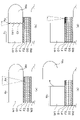
- FIG. 3 is a side view of an example of a stacked wafer being processed in a wafer processing system
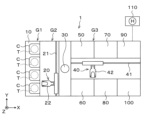
- 1 is a plan view schematically showing the outline of the configuration of a wafer processing system
- FIG. FIG. 2 is an explanatory diagram showing main steps of wafer processing
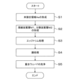
- FIG. 2 is a flow chart showing main steps of wafer processing
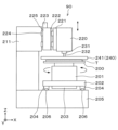
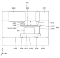
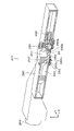
- FIG. 10 is an explanatory diagram showing the appearance of a modified edge layer formed inside the first wafer; It is a top view which shows the outline of a structure of a membrane processing apparatus. It is a side view which shows the outline of a structure of a membrane processing apparatus. It is a side view which shows the outline of a structure of a membrane processing apparatus. It is a side view which shows the outline of a structure of a membrane processing apparatus.
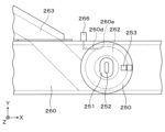
- FIG. 4 is an explanatory diagram showing the flow of atmosphere in the upper dust collection section
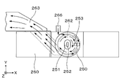
- FIG. 4 is an explanatory diagram showing the flow of atmosphere in the upper dust collection section; It is a side view which shows the outline of a structure of a lower dust collection part. It is a top view which shows the outline of a structure of a lower dust collection part. It is explanatory drawing which shows the case where a lower dust collection part is not provided as a comparative example. It is a perspective view which shows the outline of a structure of a lower dust collection part.
- FIG. 2 is an explanatory diagram showing main steps of membrane processing; FIG. 2 is a flow chart showing main steps of membrane treatment.
- wafers semiconductor substrates having a plurality of devices such as electronic circuits formed on their surfaces are bonded together. For example, thinning a first wafer forming a polymerized wafer and transferring devices formed on the first wafer to a second wafer forming a polymerized wafer.
- the peripheral edge of the wafer is chamfered.
- the peripheral part of the first wafer after thinning and the superimposed wafer after transfer is chamfered. It may have a sharply pointed shape (so-called knife-edge shape). As a result, chipping may occur at the peripheral edge of these wafers, and the wafers may be damaged. Therefore, a so-called edge trim is performed to remove the peripheral portion of the first wafer before processing.
- unnecessary surface films and particles remain on the surface of the second wafer after edge trimming, specifically, on the periphery of the second wafer exposed by removing the first wafer. These surface films and particles may flake off, drop, or scatter during transfer or processing of the polymerized wafers, thereby contaminating the interior of the wafer processing system, the interior of the cassette, or other polymerized wafers. Therefore, after edge trimming, removal of the surface film at the periphery of the second wafer is performed.
- the surface film of the peripheral portion is removed by irradiating it with a laser beam.
- laser light is used in this manner, fine dust is generated by laser processing (ablation processing). If dust adheres to the condensing lens of the laser beam, the processing quality will be degraded. In addition, when dust adheres to the wafer surface, the production yield of product wafers decreases. Furthermore, if dust adheres to the wafer processing equipment, the operating rate will decrease.
- the laser processing apparatus (wafer processing apparatus) disclosed in Patent Document 1 is equipped with dust discharging means for collecting and discharging dust generated during laser processing.
- the dust discharge means is provided at the lower end of the collector, ie the dust discharge means and the collector are integrated. Also, the dust discharging means and the collector are configured to be movable integrally.
- a wafer processing system including a film processing apparatus as a substrate processing apparatus and a wafer processing method as a substrate processing method according to the present embodiment will be described below with reference to the drawings.
- elements having substantially the same functional configuration are denoted by the same reference numerals, thereby omitting redundant description.
- processing is performed on a superimposed wafer T as a substrate in which a first wafer W1 and a second wafer W2 are bonded as shown in FIG. Then, in the wafer processing system 1, the peripheral portion We of the first wafer W1 is removed.
- the surface of the first wafer W1 that is bonded to the second wafer W2 is referred to as a front surface W1a
- the surface opposite to the front surface W1a is referred to as a rear surface W1b.
- the surface on the side bonded to the first wafer W1 is called a front surface W2a, and the surface opposite to the front surface W2a is called a back surface W2b.
- a region radially inward of the peripheral edge portion We to be removed is referred to as a central portion Wc.
- the first wafer W1 is, for example, a semiconductor wafer such as a silicon substrate, and a device layer D1 including a plurality of devices is formed on the surface W1a.
- a bonding film F1 is further formed on the device layer D1, and is bonded to the second wafer W2 via the bonding film F1.
- Examples of the bonding film F1 include oxide films (SiO 2 film, TEOS film), SiC films, SiCN films, adhesives, and the like.
- the peripheral edge portion We of the first wafer W1 is chamfered, and the thickness of the cross section of the peripheral edge portion We decreases toward its tip.
- peripheral edge portion We is a portion to be removed in the edge trim described later, and is, for example, within a range of 0.5 mm to 5 mm in the radial direction from the outer end portion of the first wafer W1.
- a laser absorption layer (not shown) capable of absorbing the laser beam irradiated inside the superposed wafer T when removing the peripheral portion We.
- the bonding film F1 formed on the device layer D1 may be used as a laser absorption layer.
- the second wafer W2 has, for example, the same configuration as the first wafer W1, a device layer D2 and a bonding film F2 are formed on the surface W2a, and the peripheral edge is chamfered.
- the second wafer W2 does not have to be a device wafer on which the device layer D2 is formed, and may be, for example, a support wafer that supports the first wafer W1. In such a case, the second wafer W2 functions as a protective material that protects the device layer D1 of the first wafer W1.
- the device layers D1 and D2 and the bonding films F1 and F2 formed on the first wafer W1 and the second wafer W2 are sometimes referred to as "surface films".
- a plurality of surface films are laminated on the first wafer W1 and the second wafer W2 according to the present embodiment.
- the wafer processing system 1 has a configuration in which a loading/unloading block G1, a transfer block G2, and a processing block G3 are integrally connected.
- the loading/unloading block G1, the transport block G2, and the processing block G3 are arranged side by side in this order from the X-axis negative direction side.
- the loading/unloading block G1 loads/unloads a cassette C capable of accommodating a plurality of superposed wafers T to/from the outside.
- a cassette mounting table 10 is provided in the loading/unloading block G1.
- a plurality of, for example, four cassettes C can be placed in a row on the cassette placing table 10 in the Y-axis direction.
- the number of cassettes C to be placed on the cassette placing table 10 is not limited to that of the present embodiment, and can be arbitrarily determined.
- the transfer block G2 is provided with a wafer transfer device 20 adjacent to the cassette mounting table 10 on the X-axis positive direction side of the cassette mounting table 10 .
- the wafer transfer device 20 is configured to be movable on a transfer path 21 extending in the Y-axis direction.
- the wafer transfer device 20 also has, for example, two transfer arms 22, 22 that hold and transfer the superposed wafer T. As shown in FIG.
- Each transport arm 22 is configured to be movable in the horizontal direction, the vertical direction, around the horizontal axis, and around the vertical axis. Note that the configuration of the transport arm 22 is not limited to the present embodiment, and may take any configuration.
- the wafer transfer device 20 is configured to transfer the overlapped wafers T to the cassette C on the cassette mounting table 10 and the transition device 30, which will be described later.
- the transfer block G2 is provided with a transition device 30 for transferring the overlapped wafer T adjacent to the wafer transfer device 20 on the positive X-axis side of the wafer transfer device 20 .
- the processing block G3 has a wafer transfer device 40, a cleaning device 50, a peripheral removal device 60, an interface reforming device 70, an internal reforming device 80, a film processing device 90 as a substrate processing device, and an inspection device 100. .
- the wafer transfer device 40 is configured to be movable on a transfer path 41 extending in the X-axis direction. Further, the wafer transfer device 40 has, for example, two transfer arms 42, 42 that hold and transfer the superposed wafer T. As shown in FIG. Each transport arm 42 is configured to be movable in the horizontal direction, the vertical direction, around the horizontal axis, and around the vertical axis. Note that the configuration of the transport arm 42 is not limited to this embodiment, and may take any configuration.
- the wafer transfer device 40 is configured to transfer the overlapped wafer T to the transition device 30, the cleaning device 50, the edge removing device 60, the interface reforming device 70, the internal reforming device 80, and the film processing device 90. It is
- the cleaning device 50 cleans the polymerized wafer T.
- the peripheral edge removal device 60 removes the peripheral edge portion We of the first wafer W1, that is, performs edge trimming.
- the interface reforming device 70 irradiates the interface between the first wafer W1 and the second wafer W2 with laser light (interface laser light, eg, CO 2 laser) to form an unbonded area Ae, which will be described later.
- the internal reforming device 80 irradiates the inside of the first wafer W1 with a laser beam (an internal laser beam, for example, a YAG laser), the peripheral edge reforming layer M1 serving as a starting point for peeling of the peripheral edge portion We, and the peripheral edge portion We.
- a laser beam an internal laser beam, for example, a YAG laser
- a divided modified layer M2 is formed as a starting point for breaking into small pieces.
- the film processing apparatus 90 irradiates laser light (film processing laser light, for example, CO 2 laser or IR laser) to the surface film (residual film) exposed at the peripheral portion of the second wafer W2 by the edge trim processing. .
- laser light film processing laser light, for example, CO 2 laser or IR laser
- the inspection apparatus 100 inspects the peripheral edge of the first wafer W1 after forming the unbonded area Ae or the peripheral edge of the second wafer W2 after film processing.
- a controller 110 is provided in the wafer processing system 1 described above.
- the control device 110 is, for example, a computer equipped with a CPU, memory, etc., and has a program storage unit (not shown).
- the program storage unit stores programs for controlling the processing of the superposed wafers T in the wafer processing system 1 .
- the program may be recorded in a computer-readable storage medium H and installed in the control device 110 from the storage medium H. Further, the storage medium H may be temporary or non-temporary.
- a bonding apparatus outside the wafer processing system 1 bonds the first wafer W1 and the second wafer W2 to form a superimposed wafer T in advance.
- a cassette C containing a plurality of superposed wafers T is mounted on the cassette mounting table 10 of the loading/unloading block G1.
- the superposed wafer T in the cassette C is taken out by the wafer transfer device 20 .
- the superposed wafer T taken out from the cassette C is transferred to the wafer transfer device 40 via the transition device 30 and then transferred to the interface modification device 70 .
- the interface modification apparatus 70 as shown in FIG. 3A, the interface (more specifically, the interface) between the first wafer W1 and the device layer D1 is changed while rotating the superposed wafer T (first wafer W1).
- a laser beam (for example, a CO 2 laser having a wavelength of 8.9 ⁇ m to 11 ⁇ m) is irradiated onto the above-described laser absorption layer formed on the substrate) to form an unbonded region Ae (step S1 in FIG. 4).
- the interface between the first wafer W1 and the device layer D1 is modified or separated, and the bonding strength between the first wafer W1 and the second wafer W2 is reduced or eliminated.
- the annular unbonded region Ae and the first wafer W1 and the second wafer W2 are bonded radially inside the unbonded region Ae.
- a junction region Ac is formed.
- edge trimming which will be described later, the peripheral edge portion We of the first wafer W1 to be removed is removed, but the existence of the unbonded region Ae in this way makes it possible to properly remove the peripheral edge portion We. can be done.
- the superposed wafer T on which the unbonded area Ae is formed is next transferred to the internal reforming device 80 by the wafer transfer device 40 .
- the peripheral reformed layer M1 and the divided reformed layers M2 are formed inside the first wafer W1 (step S2 in FIG. 4).
- the modified peripheral layer M1 serves as a base point for removing the peripheral edge portion We in edge trimming, which will be described later.
- the divided modified layer M2 serves as a starting point for dividing the peripheral portion We to be removed into small pieces. Note that in the drawings used for the following description, the illustration of the divided modified layer M2 may be omitted in order to avoid complication of the illustration.
- cracks C1 extend in the thickness direction of the first wafer W1 from the modified peripheral layer M1 formed inside the first wafer W1, as shown in FIG. 3(b).
- the lower end of the crack C1 reaches, for example, the surface W1a of the first wafer W1 or the unbonded area Ae.
- the superposed wafer T in which the modified edge layer M1 and the divided modified layer M2 are formed inside the first wafer W1 is then transferred to the edge removing apparatus 60 by the wafer transfer apparatus 40.
- the peripheral edge removal device 60 removes the peripheral edge portion We of the first wafer W1, that is, edge trim processing is performed (step S3 in FIG. 4).
- the peripheral portion We is separated from the central portion Wc of the first wafer W1 with the modified peripheral layer M1 and the crack C1 as starting points, and the device layer D1 (second wafer W2 ).
- the peripheral portion We to be removed is divided into small pieces with the divided modified layer M2 and the crack C2 as base points.
- a wedge-shaped blade for example, may be inserted into the interface between the first wafer W1 and the second wafer W2 forming the overlapped wafer T.
- edge trimming by applying impact to the peripheral edge portion We of the first wafer W1, the peripheral edge portion We is appropriately peeled off from the modified peripheral edge layer M1 and the crack C1 as a starting point.
- the superposed wafer T from which the peripheral portion We of the first wafer W1 has been removed is then transferred to the film processing apparatus 90 by the wafer transfer apparatus 40.
- the film processing apparatus 90 as shown in FIG. 3(d), processing for removing the surface film on the peripheral portion of the second wafer W2 after the peripheral portion We has been removed (hereinafter sometimes referred to as “film processing”). Yes.) is performed (step S4 in FIG. 4).
- step S4 the surface film on the peripheral portion of the second wafer W2 is removed in order to suppress scattering of the surface film and particles after the removal of the peripheral portion We. That is, for example, the surface film is irradiated with laser light (for example, CO 2 laser) to remove the surface film.
- laser light for example, CO 2 laser
- the superposed wafer T from which the surface film on the peripheral edge of the second wafer W2 has been removed is then transferred to the cleaning device 50 by the wafer transfer device 40.
- the peripheral portion We is removed, and the rear surface W1b and the exposed portion of the first wafer W1 after the film processing are cleaned (step S5 in FIG. 4).
- the back surface W2b of the second wafer W2 may be cleaned together with the back surface W1b of the first wafer W1.
- the superposed wafer T which has undergone all the wafer processing, is transferred to the cassette C on the cassette mounting table 10 by the wafer transfer device 20 via the transition device 30 .
- the wafer transfer device 20 via the transition device 30 .
- the film processing apparatus 90 has a chuck 200 as a substrate holding section that holds the superimposed wafer T on its upper surface.
- the chuck 200 sucks and holds the rear surface W2b of the second wafer W2 in a state in which the first wafer W1 is arranged on the upper side and the second wafer W2 is arranged on the lower side.
- Chuck 200 is supported by slider table 202 via air bearing 201 .
- a rotating portion 203 is provided on the lower surface side of the slider table 202 .
- the rotating part 203 incorporates, for example, a motor as a drive source.
- the chuck 200 is configured to be rotatable about a vertical axis via an air bearing 201 by a rotating portion 203 .
- the slider table 202 is configured to be movable on a rail 206 extending in the Y-axis direction on a base 205 via a moving portion 204 provided on the underside thereof.
- the driving source of the moving unit 204 is not particularly limited, for example, a linear motor is used.
- a macro camera 210 is provided above the chuck 200 .
- the macro camera 210 is supported by a support column 211 .
- Macro camera 210 images the outer edge of second wafer W2.
- the macro camera 210 includes, for example, a coaxial lens, emits infrared light (IR light), and receives reflected light from an object.
- IR light infrared light
- the imaging magnification of the macro camera 210 is 2 times.
- An image captured by macro camera 210 is output to control device 110 .
- the controller 110 calculates the amount of eccentricity between the center of the chuck 200 and the center of the second wafer W2 from the image captured by the macro camera 210 .
- a laser irradiation unit 220 for irradiating the superposed wafer T held by the chuck 200 with laser light.
- the laser irradiation unit 220 is connected to a laser head (not shown) containing a laser oscillator (not shown) that oscillates laser light.
- the laser irradiation section 220 is supported by a support member 221 .
- the laser irradiation unit 220 is configured to be vertically movable by means of a lifting unit 223 along a rail 222 extending in the vertical direction.
- the laser irradiation unit 220 is configured to be movable in the Y-axis direction by a moving unit 225 along a rail 224 extending in the Y-axis direction on the support column 211 .
- the laser irradiation unit 220 irradiates the surface film on the peripheral edge of the second wafer W2 with laser light to remove the surface film.
- the laser irradiation section 220 has a condenser lens 231 and a nozzle 232 .
- the condenser lens 231 collects laser light emitted from the laser oscillator of the laser head and irradiates the laser light onto the peripheral surface film of the second wafer W2.
- the nozzle 232 is provided below the condensing lens 231 .
- the nozzle 232 is a hollow cylindrical member that allows the laser light from the condenser lens 231 to pass therethrough and irradiate the surface film on the peripheral edge of the second wafer W2.
- a first air supply section 233 for supplying gas such as dry air to the inside of the nozzle 232 is provided above the nozzle 232 .
- the first air supply portion 233 communicates with an air supply passage 232 a formed inside the side wall of the nozzle 232 .
- the gas supplied from the first air supply part 233 and the air supply path 232a flows downward through the nozzle 232 and is sprayed onto the surface film of the peripheral edge of the second wafer W2.
- Such gas can prevent dust generated by laser processing from adhering to the condenser lens 231 .
- the membrane processing apparatus 90 has a dust collector 240 for collecting dust.
- the dust collection unit 240 collects fine particles generated during the film processing (during laser processing) in step S4 described above, that is, when the laser beam is irradiated from the laser irradiation unit 220 to the surface film on the peripheral edge of the second wafer W2. collect dust.
- the dust collection section 240 has an upper dust collection section 241 and a lower dust collection section 242 .
- the upper dust collection section 241 is provided above the chuck 200 and directly below the laser irradiation section 220 . As shown in FIGS. 10 and 11, the upper dust collecting section 241 has a sleeve 250 and an exhaust duct 260. As shown in FIGS. The sleeve 250 is provided on the upper surface of the exhaust duct 260 .
- the sleeve 250 has a substantially truncated cone shape whose diameter decreases from the top to the bottom.
- a housing portion 251 that houses a part of the nozzle 232 of the laser irradiation portion 220 is formed in the central portion of the upper surface of the sleeve 250 .
- the nozzle 232 can move up and down with respect to the accommodation portion 251 and enter or exit the accommodation portion 251 .
- the laser head is provided with a power meter (not shown) for checking the output of the laser beam, but the output of the laser beam cannot be measured while the dust collector 240 is exhausting. Therefore, in such a case, the nozzle 232 is withdrawn from the accommodating portion 251 .
- the nozzle 232 is housed in the housing portion 251 .
- the nozzle 232 is movable in the Y-axis direction in the accommodation portion 251 . Further, the nozzle 232 is rotatable at its lower end with its upper end as a base point. Note that the nozzle 232 does not contact the accommodation portion 251 while being accommodated in the accommodation portion 251 .
- the nozzle 232 is movable in the Y-axis direction, and in order to be movable during laser processing, as shown in FIG. You may have Further, an elongated hole 252 is formed in the lower surface of the housing portion 251 for passing the laser beam emitted from the nozzle 232. Even if this elongated hole 252 also has a long axis in the Y-axis direction, good. As will be described later, the moving distance of the nozzle 232 is, for example, 2 mm to 5 mm when performing film processing. Therefore, the length of the long hole 252 in the Y-axis direction is preferably 5 mm or more.
- a second air supply portion 253 is provided to supply gas such as dry air to an intake passage 262, which will be described later. ing.
- the second air supply portion 253 communicates with an air supply passage 250a that penetrates the sleeve 250 from the upper surface to the lower surface.
- the air supply path 250 a is connected to a discharge portion 250 b formed on the lower surface of the sleeve 250 .
- the gas supplied from the discharge section 250 b through the second air supply section 253 and the air supply path 250 a flows out to the intake flow path 262 .
- Such gas blows off fumes generated by laser processing.
- the gas from the second air supply section 253 guides the atmosphere of the intake flow path 262 to the exhaust flow path 263, which will be described later. At this time, the fumes are also guided to the exhaust passage 263 .
- the overlapping wafer T is irradiated with laser light while the overlapping wafer T is being rotated.
- the gas from the second air supply part 253, the air supply path 250a and the discharge part 250b is preferably supplied in the rotation direction of the superposed wafer T. As shown in FIG. In such a case, the atmosphere in the air intake channel 262 can be more reliably guided to the exhaust channel 263 .
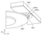
- the exhaust duct 260 is provided extending in the X-axis direction. As shown in FIGS. 11 and 13, an opening 261 is formed below the sleeve 250 on the lower surface 260a of the exhaust duct 260 to allow the laser beam emitted from the nozzle 232 to pass therethrough.
- the lower surface 260a has a substantially circular shape in plan view.
- An intake passage 262 and an exhaust passage 263 are formed inside the exhaust duct 260 .
- the intake channel 262 is a channel formed between the sleeve 250 and the opening 261 .
- the suction flow path 262 sucks the atmosphere between the superposed wafer T held by the chuck 200 and the exhaust duct 260 through the opening 261 .
- the exhaust channel 263 is a channel that communicates with the intake channel 262 and extends in the tangential direction of the superposed wafer T, that is, in the X-axis direction.
- the exhaust passage 263 communicates with an exhaust pipe 264 provided at the end of the exhaust duct 260 on the negative side of the X-axis.
- the exhaust pipe 264 is connected to an exhaust device (not shown) that sucks the internal atmosphere of the exhaust duct 260 .
- a third air supply section 265 for supplying gas such as dry air is provided inside the exhaust duct 260 on the X-axis positive direction side of the accommodation section 251 .
- the third air supply portion 265 communicates with an air supply passage 260b formed through the side wall of the exhaust duct 260 toward the bottom surface.
- the air supply path 260b is connected to a discharge portion 260c formed on the lower surface 260a of the exhaust duct 260 .
- a plurality of discharge portions 260 c are provided around the opening 261 on the lower surface 260 a of the exhaust duct 260 .
- a plurality of ejection portions 260c are provided at equal intervals on a concentric circle with the opening portion 261, that is, the radial distances between each ejection portion 260c and the lower surface 260a are equal. Therefore, the atmosphere between the exhaust duct 260 and the superposed wafer T is uniformly sucked through the opening 261 .
- the gas supplied from the third air supply portion 265, the air supply passage 260b and the discharge portion 260c is ejected downward around the opening 261 to form a so-called air curtain.
- dust generated by laser processing is suppressed from flowing out of the air curtain.
- the gas from the third air supply part 265, the air supply path 260b and the discharge part 260c passes through the opening 261 to the intake flow path 262. flow into In such a case, the dust also flows into the air intake passage 262 through the opening 261, so that the dust can be reliably collected in the exhaust duct 260.
- the number of air supply passages 260b on the lower surface 260a of the exhaust duct 260 is not limited, the greater the number, the higher the effect of the air curtain.
- a fourth air supply section 266 for supplying gas such as dry air is provided on the side surface of the exhaust duct 260 on the positive Y-axis side of the accommodation section 251 .
- the fourth air supply portion 266 communicates with an air supply passage 260 d penetrating from the side wall of the exhaust duct 260 toward the intake passage 262 .
- the air supply path 260 d is connected to a discharge portion 260 e formed on the inner surface of the exhaust duct 260 .
- the air supply passage 260d and the discharge portion 260e are formed in the positive direction of the X-axis with respect to the air intake passage 262, for example.
- the gas supplied from the fourth air supply portion 266, the air supply passage 260d, and the discharge portion 260e flows into the intake passage 262 and forms a swirling flow in the intake passage 262.
- the positions of the air supply passage 260d and the discharge portion 260e are not limited to those of the present embodiment as long as they are positions capable of forming a swirling flow in the intake passage 262.
- the atmosphere between the exhaust duct 260 and the superposed wafer T is sucked into the exhaust duct 260 through the opening 261, and furthermore, the air intake passage 262 and the exhaust flow It flows through passage 263 and is discharged from exhaust pipe 264 . Dust generated by laser processing is also collected along with this airflow.
- the gas from the second air supply part 253 blows off the fumes generated by the laser processing and guides them to the exhaust flow path 263 .
- the gas from the third air supply section 265 suppresses dust from flowing out to the outside.
- the gas from the fourth air supply section 266 forms a swirling flow in the air intake channel 262 , and smoothly guides the atmosphere and dust to the exhaust channel 263 .
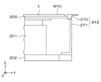
- the lower dust collecting portion 242 has a dust collecting plate 270 and a support member 271.
- the dust collection plate 270 is provided close to the outer circumference of the chuck 200 .
- a gap between the dust collection plate 270 and the outer periphery of the chuck 200 is, for example, 0.5 mm or less. The narrower the gap, the more it is possible to suppress the outflow of dust.
- the height of the upper surface of the dust collection plate 270 is preferably the same as the height of the upper surface of the superposed wafer T (back surface W1b of the first wafer W1) held by the chuck 200. Further, the dust collection plate 270 is supported by a support member 271 on its lower surface. The support member 271 is fixed to the slider table 202 . That is, the lower dust collecting portion 242 is provided integrally with the chuck 200, and the lower dust collecting portion 242 also moves in the Y-axis direction as the chuck 200 moves.
- the dust collection plate 270 has a substantially rectangular shape in plan view, and an end portion 270a on the chuck 200 side is curved along the outer circumference of the chuck 200 .
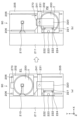
- the Y-axis direction length A of the dust collection plate 270 is greater than the diameter D of the opening 261 of the exhaust duct 260 .
- the X-axis direction length B of the dust collection plate 270 is greater than the radius D/2 of the opening 261 .
- the dust collecting plate 270 is provided so as to overlap the opening 261 in a plan view when arranged below the exhaust duct 260 of the upper dust collecting portion 241 .
- the dust collection plate 270 and the chuck 200 may contact each other.
- the peripheral edge portion of the second wafer W2 is irradiated with laser light during laser processing, in the opening portion 261, the inner side in the radial direction from the end portion of the chuck 200 (overlapped wafer T) is flat. Although it is visually covered with the chuck 200, the outer side in the radial direction is exposed from the end. As a result, the amount of dust sucked is uneven over the entire circumference of the opening 261, and the dust may not be stably collected.
- the dust collection plate 270 is provided so as to overlap the opening 261 in plan view when arranged below the exhaust duct 260 .
- the dust suction amount becomes uniform over the entire circumference of the opening 261, and the dust can be stably collected.
- the chuck 200 is placed at the standby position P1.
- the nozzle 232 is housed in the housing portion 251 of the sleeve 250 .
- the superposed wafer T is loaded into the film processing apparatus 90 and held by the chuck 200 (step T1 in FIG. 21).
- the chuck 200 is moved to the macro alignment position.
- the macro alignment position is the position where the macro camera 210 can image the outer edge of the second wafer W2.
- the macro camera 210 captures an image of the outer edge of the second wafer W2 in the circumferential direction of 360 degrees.
- the captured image is output from macro camera 210 to control device 110 .
- the controller 110 calculates the amount of eccentricity between the center of the chuck 200 and the center of the second wafer W2 from the image of the macro camera 210 . Furthermore, based on the amount of eccentricity, the controller 110 calculates the amount of movement of the chuck 200 so as to correct the Y-axis component of the amount of eccentricity. Then, the position of the chuck 200 is determined so that the center of the second wafer W2m and the center of the chuck 200 are aligned (step T2 of u22).
- the processing position P2 is a position where the end of the peripheral portion of the second wafer W2 in the positive Y-axis direction is arranged directly below the nozzle 232 of the laser irradiation unit 220 .
- the dust collection plate 270 is arranged so as to overlap the opening 261 of the exhaust duct 260 in plan view.
- the nozzle 232 is moved in the negative direction of the X-axis, and a laser beam is emitted from the nozzle 232 to the surface film on the peripheral edge of the second wafer W2. Then, the surface film is irradiated with the laser light in a spiral manner.
- the moving distance of the nozzle 232 is 2 mm to 5 mm, and the peripheral edge of the second wafer W2 to be processed is in the range of 2 mm to 5 mm from the outer edge. That is, by moving the nozzle 232, the processing width of the laser beam is adjusted. Then, the surface film is removed (step T4 in FIG. 21).
- Dust is generated during laser processing in step T4. This dust is collected in the upper dust collecting section 241 . Specifically, as described above, the atmosphere between the exhaust duct 260 and the superimposed wafer T is sucked into the exhaust duct 260 through the opening 261 and further flows through the intake channel 262 and the exhaust channel 263. and discharged from the exhaust pipe 264 . Dust generated by laser processing is also collected along with this airflow.
- the chuck 200 is moved to the standby position P1. Then, the superposed wafer T is unloaded from the film processing apparatus 90 (step T5 in FIG. 21). Thus, a series of film treatments in the film treatment apparatus 90 are completed.
- the laser irradiation unit 220 and the upper dust collection unit 241 are provided separately, compared to the case where they are integrally provided as in the related art, the exhaust of the upper dust collection unit 241 Duct 260 can be enlarged. Therefore, the dust generated during laser processing can be properly and efficiently collected by the upper dust collection part 241 .
- the condenser lens 231 can be made smaller, and the device space can be reduced. In addition, it is easy to change the focal height of the condenser lens 231, and it is possible to shorten the processing time by performing laser processing at a defocused position. Furthermore, by changing the focal height, it is possible to easily deal with variations in the height of the processing point of laser processing due to machine differences and changes in the thickness of the superposed wafer T. FIG.
- the technique of the present disclosure is applied when removing the surface film on the peripheral edge of the second wafer W2, but the technique can also be used for other purposes.
- the present disclosure can be applied.
- Technology can be applied. Even in such a case, when irradiating the peripheral portion with laser light, the same effect as in the above embodiment can be enjoyed.
Landscapes
- Engineering & Computer Science (AREA)
- Physics & Mathematics (AREA)
- Optics & Photonics (AREA)
- Plasma & Fusion (AREA)
- Mechanical Engineering (AREA)
- Laser Beam Processing (AREA)
- Mechanical Treatment Of Semiconductor (AREA)
- Cleaning In General (AREA)
- Cleaning Or Drying Semiconductors (AREA)
Priority Applications (4)
| Application Number | Priority Date | Filing Date | Title |
|---|---|---|---|
| CN202280053193.XA CN117769473A (zh) | 2021-08-06 | 2022-07-26 | 基板处理装置和基板处理方法 |
| KR1020247006512A KR20240038071A (ko) | 2021-08-06 | 2022-07-26 | 기판 처리 장치 및 기판 처리 방법 |
| JP2023540271A JP7588725B2 (ja) | 2021-08-06 | 2022-07-26 | 基板処理装置及び基板処理方法 |
| JP2024197369A JP2025013658A (ja) | 2021-08-06 | 2024-11-12 | 基板処理装置 |
Applications Claiming Priority (2)
| Application Number | Priority Date | Filing Date | Title |
|---|---|---|---|
| JP2021-130301 | 2021-08-06 | ||
| JP2021130301 | 2021-08-06 |
Publications (1)
| Publication Number | Publication Date |
|---|---|
| WO2023013468A1 true WO2023013468A1 (ja) | 2023-02-09 |
Family
ID=85154479
Family Applications (1)
| Application Number | Title | Priority Date | Filing Date |
|---|---|---|---|
| PCT/JP2022/028734 Ceased WO2023013468A1 (ja) | 2021-08-06 | 2022-07-26 | 基板処理装置及び基板処理方法 |
Country Status (5)
| Country | Link |
|---|---|
| JP (2) | JP7588725B2 (https=) |
| KR (1) | KR20240038071A (https=) |
| CN (1) | CN117769473A (https=) |
| TW (1) | TW202326839A (https=) |
| WO (1) | WO2023013468A1 (https=) |
Cited By (1)
| Publication number | Priority date | Publication date | Assignee | Title |
|---|---|---|---|---|
| US20230178374A1 (en) * | 2020-04-02 | 2023-06-08 | Tokyo Electron Limited | Substrate processing method and substrate processing apparatus |
Citations (5)
| Publication number | Priority date | Publication date | Assignee | Title |
|---|---|---|---|---|
| JPH11254169A (ja) * | 1998-03-11 | 1999-09-21 | Mitsubishi Electric Corp | レーザ加工装置 |
| JP2001321979A (ja) * | 2000-05-12 | 2001-11-20 | Matsushita Electric Ind Co Ltd | レーザー穴加工機の加工粉集塵装置 |
| JP2007069249A (ja) * | 2005-09-07 | 2007-03-22 | Disco Abrasive Syst Ltd | レーザー加工装置 |
| JP2007229722A (ja) * | 2006-02-27 | 2007-09-13 | Denso Corp | レーザ加工における飛散物の除去方法および装置 |
| WO2021131711A1 (ja) * | 2019-12-26 | 2021-07-01 | 東京エレクトロン株式会社 | 基板処理方法及び基板処理装置 |
-
2022
- 2022-07-26 WO PCT/JP2022/028734 patent/WO2023013468A1/ja not_active Ceased
- 2022-07-26 CN CN202280053193.XA patent/CN117769473A/zh active Pending
- 2022-07-26 KR KR1020247006512A patent/KR20240038071A/ko active Pending
- 2022-07-26 JP JP2023540271A patent/JP7588725B2/ja active Active
- 2022-07-26 TW TW111127890A patent/TW202326839A/zh unknown
-
2024
- 2024-11-12 JP JP2024197369A patent/JP2025013658A/ja active Pending
Patent Citations (5)
| Publication number | Priority date | Publication date | Assignee | Title |
|---|---|---|---|---|
| JPH11254169A (ja) * | 1998-03-11 | 1999-09-21 | Mitsubishi Electric Corp | レーザ加工装置 |
| JP2001321979A (ja) * | 2000-05-12 | 2001-11-20 | Matsushita Electric Ind Co Ltd | レーザー穴加工機の加工粉集塵装置 |
| JP2007069249A (ja) * | 2005-09-07 | 2007-03-22 | Disco Abrasive Syst Ltd | レーザー加工装置 |
| JP2007229722A (ja) * | 2006-02-27 | 2007-09-13 | Denso Corp | レーザ加工における飛散物の除去方法および装置 |
| WO2021131711A1 (ja) * | 2019-12-26 | 2021-07-01 | 東京エレクトロン株式会社 | 基板処理方法及び基板処理装置 |
Cited By (2)
| Publication number | Priority date | Publication date | Assignee | Title |
|---|---|---|---|---|
| US20230178374A1 (en) * | 2020-04-02 | 2023-06-08 | Tokyo Electron Limited | Substrate processing method and substrate processing apparatus |
| US12381085B2 (en) * | 2020-04-02 | 2025-08-05 | Tokyo Electron Limited | Bonded substrate peripheral laser processing method and substrate processing apparatus thereof |
Also Published As
| Publication number | Publication date |
|---|---|
| CN117769473A (zh) | 2024-03-26 |
| TW202326839A (zh) | 2023-07-01 |
| JP7588725B2 (ja) | 2024-11-22 |
| JP2025013658A (ja) | 2025-01-24 |
| JPWO2023013468A1 (https=) | 2023-02-09 |
| KR20240038071A (ko) | 2024-03-22 |
Similar Documents
| Publication | Publication Date | Title |
|---|---|---|
| JP7720426B2 (ja) | 基板処理方法 | |
| TWI870947B (zh) | 基板處理系統及基板處理方法 | |
| JP7413468B2 (ja) | 基板処理装置及び基板処理方法 | |
| JP6739873B2 (ja) | ウェーハの加工方法 | |
| KR20240073916A (ko) | 처리 방법 및 처리 시스템 | |
| WO2020184178A1 (ja) | 処理装置及び処理方法 | |
| JP2025013658A (ja) | 基板処理装置 | |
| WO2023176519A1 (ja) | 基板処理装置及び基板処理方法 | |
| JP2020072238A (ja) | 基板処理装置及び基板処理方法 | |
| JP7749016B2 (ja) | 基板処理装置及び基板処理方法 | |
| JP2023003476A (ja) | 処理方法及び処理システム | |
| JP2020198367A (ja) | 基板処理システム及び基板処理方法 | |
| JP2024087506A (ja) | 基板処理方法及びウェハ処理システム | |
| KR20260052193A (ko) | 기판 가공 장치 및 기판 가공 방법 |
Legal Events
| Date | Code | Title | Description |
|---|---|---|---|
| 121 | Ep: the epo has been informed by wipo that ep was designated in this application |
Ref document number: 22852892 Country of ref document: EP Kind code of ref document: A1 |
|
| WWE | Wipo information: entry into national phase |
Ref document number: 2023540271 Country of ref document: JP |
|
| WWE | Wipo information: entry into national phase |
Ref document number: 202280053193.X Country of ref document: CN |
|
| ENP | Entry into the national phase |
Ref document number: 20247006512 Country of ref document: KR Kind code of ref document: A |
|
| NENP | Non-entry into the national phase |
Ref country code: DE |
|
| 122 | Ep: pct application non-entry in european phase |
Ref document number: 22852892 Country of ref document: EP Kind code of ref document: A1 |