WO2022270633A1 - 非接触通信媒体 - Google Patents
非接触通信媒体 Download PDFInfo
- Publication number
- WO2022270633A1 WO2022270633A1 PCT/JP2022/025387 JP2022025387W WO2022270633A1 WO 2022270633 A1 WO2022270633 A1 WO 2022270633A1 JP 2022025387 W JP2022025387 W JP 2022025387W WO 2022270633 A1 WO2022270633 A1 WO 2022270633A1
- Authority
- WO
- WIPO (PCT)
- Prior art keywords
- housing
- lid
- communication medium
- fixture
- peripheral surface
- Prior art date
Links
- 238000004891 communication Methods 0.000 title claims abstract description 88
- 238000007789 sealing Methods 0.000 claims description 57
- 230000002093 peripheral effect Effects 0.000 claims description 41
- 239000011810 insulating material Substances 0.000 claims description 25
- 238000013459 approach Methods 0.000 claims description 6
- 238000000034 method Methods 0.000 claims description 5
- 230000035699 permeability Effects 0.000 claims description 3
- 230000005499 meniscus Effects 0.000 claims description 2
- 239000000463 material Substances 0.000 description 49
- 239000002585 base Substances 0.000 description 46
- 239000007788 liquid Substances 0.000 description 27
- 238000012986 modification Methods 0.000 description 22
- 230000004048 modification Effects 0.000 description 22
- 239000007789 gas Substances 0.000 description 19
- 239000000919 ceramic Substances 0.000 description 17
- 229910052751 metal Inorganic materials 0.000 description 16
- 239000002184 metal Substances 0.000 description 16
- 230000001012 protector Effects 0.000 description 15
- 229920006015 heat resistant resin Polymers 0.000 description 14
- 229910052878 cordierite Inorganic materials 0.000 description 9
- JSKIRARMQDRGJZ-UHFFFAOYSA-N dimagnesium dioxido-bis[(1-oxido-3-oxo-2,4,6,8,9-pentaoxa-1,3-disila-5,7-dialuminabicyclo[3.3.1]nonan-7-yl)oxy]silane Chemical compound [Mg++].[Mg++].[O-][Si]([O-])(O[Al]1O[Al]2O[Si](=O)O[Si]([O-])(O1)O2)O[Al]1O[Al]2O[Si](=O)O[Si]([O-])(O1)O2 JSKIRARMQDRGJZ-UHFFFAOYSA-N 0.000 description 9
- -1 PBO Substances 0.000 description 8
- 239000004693 Polybenzimidazole Substances 0.000 description 8
- 229920002480 polybenzimidazole Polymers 0.000 description 8
- 239000012790 adhesive layer Substances 0.000 description 7
- 239000000843 powder Substances 0.000 description 6
- 239000004696 Poly ether ether ketone Substances 0.000 description 5
- 229920002530 polyetherether ketone Polymers 0.000 description 5
- 230000001681 protective effect Effects 0.000 description 5
- 239000000853 adhesive Substances 0.000 description 4
- 230000001070 adhesive effect Effects 0.000 description 4
- 238000004519 manufacturing process Methods 0.000 description 4
- 238000007747 plating Methods 0.000 description 4
- HBMJWWWQQXIZIP-UHFFFAOYSA-N silicon carbide Chemical compound [Si+]#[C-] HBMJWWWQQXIZIP-UHFFFAOYSA-N 0.000 description 4
- 229910010271 silicon carbide Inorganic materials 0.000 description 4
- 238000003860 storage Methods 0.000 description 4
- 229910018072 Al 2 O 3 Inorganic materials 0.000 description 3
- 229910008556 Li2O—Al2O3—SiO2 Inorganic materials 0.000 description 3
- RTAQQCXQSZGOHL-UHFFFAOYSA-N Titanium Chemical compound [Ti] RTAQQCXQSZGOHL-UHFFFAOYSA-N 0.000 description 3
- 230000004308 accommodation Effects 0.000 description 3
- 239000012298 atmosphere Substances 0.000 description 3
- 238000005219 brazing Methods 0.000 description 3
- 230000014509 gene expression Effects 0.000 description 3
- 239000011521 glass Substances 0.000 description 3
- 239000000203 mixture Substances 0.000 description 3
- 229920005989 resin Polymers 0.000 description 3
- 239000011347 resin Substances 0.000 description 3
- 229910001220 stainless steel Inorganic materials 0.000 description 3
- 239000010935 stainless steel Substances 0.000 description 3
- 239000000126 substance Substances 0.000 description 3
- 239000010936 titanium Substances 0.000 description 3
- 229910052719 titanium Inorganic materials 0.000 description 3
- 239000002253 acid Substances 0.000 description 2
- 239000003513 alkali Substances 0.000 description 2
- 230000005540 biological transmission Effects 0.000 description 2
- 238000005246 galvanizing Methods 0.000 description 2
- 239000008187 granular material Substances 0.000 description 2
- 238000010438 heat treatment Methods 0.000 description 2
- 239000011490 mineral wool Substances 0.000 description 2
- 230000035515 penetration Effects 0.000 description 2
- 230000008569 process Effects 0.000 description 2
- 239000002994 raw material Substances 0.000 description 2
- 230000035939 shock Effects 0.000 description 2
- 238000005245 sintering Methods 0.000 description 2
- 238000002834 transmittance Methods 0.000 description 2
- 229910000505 Al2TiO5 Inorganic materials 0.000 description 1
- IJGRMHOSHXDMSA-UHFFFAOYSA-N Atomic nitrogen Chemical compound N#N IJGRMHOSHXDMSA-UHFFFAOYSA-N 0.000 description 1
- 229920003043 Cellulose fiber Polymers 0.000 description 1
- 229910052581 Si3N4 Inorganic materials 0.000 description 1
- VYPSYNLAJGMNEJ-UHFFFAOYSA-N Silicium dioxide Chemical compound O=[Si]=O VYPSYNLAJGMNEJ-UHFFFAOYSA-N 0.000 description 1
- 239000004115 Sodium Silicate Substances 0.000 description 1
- 230000002378 acidificating effect Effects 0.000 description 1
- 230000009471 action Effects 0.000 description 1
- 229910000272 alkali metal oxide Inorganic materials 0.000 description 1
- 229910052784 alkaline earth metal Inorganic materials 0.000 description 1
- 150000001342 alkaline earth metals Chemical class 0.000 description 1
- PNEYBMLMFCGWSK-UHFFFAOYSA-N aluminium oxide Inorganic materials [O-2].[O-2].[O-2].[Al+3].[Al+3] PNEYBMLMFCGWSK-UHFFFAOYSA-N 0.000 description 1
- 239000011230 binding agent Substances 0.000 description 1
- 230000015572 biosynthetic process Effects 0.000 description 1
- BRPQOXSCLDDYGP-UHFFFAOYSA-N calcium oxide Chemical compound [O-2].[Ca+2] BRPQOXSCLDDYGP-UHFFFAOYSA-N 0.000 description 1
- 239000000292 calcium oxide Substances 0.000 description 1
- ODINCKMPIJJUCX-UHFFFAOYSA-N calcium oxide Inorganic materials [Ca]=O ODINCKMPIJJUCX-UHFFFAOYSA-N 0.000 description 1
- 229910000420 cerium oxide Inorganic materials 0.000 description 1
- 239000003795 chemical substances by application Substances 0.000 description 1
- 229910001873 dinitrogen Inorganic materials 0.000 description 1
- 230000000694 effects Effects 0.000 description 1
- 230000005674 electromagnetic induction Effects 0.000 description 1
- 238000005516 engineering process Methods 0.000 description 1
- 238000011049 filling Methods 0.000 description 1
- 239000011491 glass wool Substances 0.000 description 1
- 230000006872 improvement Effects 0.000 description 1
- 239000004615 ingredient Substances 0.000 description 1
- 238000009434 installation Methods 0.000 description 1
- 230000009545 invasion Effects 0.000 description 1
- 238000005304 joining Methods 0.000 description 1
- FUJCRWPEOMXPAD-UHFFFAOYSA-N lithium oxide Chemical compound [Li+].[Li+].[O-2] FUJCRWPEOMXPAD-UHFFFAOYSA-N 0.000 description 1
- 229910001947 lithium oxide Inorganic materials 0.000 description 1
- HCWCAKKEBCNQJP-UHFFFAOYSA-N magnesium orthosilicate Chemical compound [Mg+2].[Mg+2].[O-][Si]([O-])([O-])[O-] HCWCAKKEBCNQJP-UHFFFAOYSA-N 0.000 description 1
- 239000000395 magnesium oxide Substances 0.000 description 1
- CPLXHLVBOLITMK-UHFFFAOYSA-N magnesium oxide Inorganic materials [Mg]=O CPLXHLVBOLITMK-UHFFFAOYSA-N 0.000 description 1
- 239000000391 magnesium silicate Substances 0.000 description 1
- 229910052919 magnesium silicate Inorganic materials 0.000 description 1
- 235000019792 magnesium silicate Nutrition 0.000 description 1
- AXZKOIWUVFPNLO-UHFFFAOYSA-N magnesium;oxygen(2-) Chemical compound [O-2].[Mg+2] AXZKOIWUVFPNLO-UHFFFAOYSA-N 0.000 description 1
- 239000007769 metal material Substances 0.000 description 1
- 238000002156 mixing Methods 0.000 description 1
- 238000000465 moulding Methods 0.000 description 1
- TWNQGVIAIRXVLR-UHFFFAOYSA-N oxo(oxoalumanyloxy)alumane Chemical compound O=[Al]O[Al]=O TWNQGVIAIRXVLR-UHFFFAOYSA-N 0.000 description 1
- BMMGVYCKOGBVEV-UHFFFAOYSA-N oxo(oxoceriooxy)cerium Chemical compound [Ce]=O.O=[Ce]=O BMMGVYCKOGBVEV-UHFFFAOYSA-N 0.000 description 1
- SIWVEOZUMHYXCS-UHFFFAOYSA-N oxo(oxoyttriooxy)yttrium Chemical compound O=[Y]O[Y]=O SIWVEOZUMHYXCS-UHFFFAOYSA-N 0.000 description 1
- 239000004014 plasticizer Substances 0.000 description 1
- 229920001721 polyimide Polymers 0.000 description 1
- 239000009719 polyimide resin Substances 0.000 description 1
- 238000012545 processing Methods 0.000 description 1
- AABBHSMFGKYLKE-SNAWJCMRSA-N propan-2-yl (e)-but-2-enoate Chemical compound C\C=C\C(=O)OC(C)C AABBHSMFGKYLKE-SNAWJCMRSA-N 0.000 description 1
- 238000010298 pulverizing process Methods 0.000 description 1
- 229910001404 rare earth metal oxide Inorganic materials 0.000 description 1
- HQVNEWCFYHHQES-UHFFFAOYSA-N silicon nitride Chemical compound N12[Si]34N5[Si]62N3[Si]51N64 HQVNEWCFYHHQES-UHFFFAOYSA-N 0.000 description 1
- 229910052814 silicon oxide Inorganic materials 0.000 description 1
- 239000002002 slurry Substances 0.000 description 1
- KKCBUQHMOMHUOY-UHFFFAOYSA-N sodium oxide Chemical compound [O-2].[Na+].[Na+] KKCBUQHMOMHUOY-UHFFFAOYSA-N 0.000 description 1
- 229910001948 sodium oxide Inorganic materials 0.000 description 1
- NTHWMYGWWRZVTN-UHFFFAOYSA-N sodium silicate Chemical compound [Na+].[Na+].[O-][Si]([O-])=O NTHWMYGWWRZVTN-UHFFFAOYSA-N 0.000 description 1
- 229910052911 sodium silicate Inorganic materials 0.000 description 1
- 239000002904 solvent Substances 0.000 description 1
- 238000001694 spray drying Methods 0.000 description 1
- 239000000758 substrate Substances 0.000 description 1
- 229920001187 thermosetting polymer Polymers 0.000 description 1
- 238000012546 transfer Methods 0.000 description 1
- XLYOFNOQVPJJNP-UHFFFAOYSA-N water Substances O XLYOFNOQVPJJNP-UHFFFAOYSA-N 0.000 description 1
- 238000003466 welding Methods 0.000 description 1
Images


Classifications
-
- G—PHYSICS
- G06—COMPUTING; CALCULATING OR COUNTING
- G06K—GRAPHICAL DATA READING; PRESENTATION OF DATA; RECORD CARRIERS; HANDLING RECORD CARRIERS
- G06K19/00—Record carriers for use with machines and with at least a part designed to carry digital markings
- G06K19/06—Record carriers for use with machines and with at least a part designed to carry digital markings characterised by the kind of the digital marking, e.g. shape, nature, code
- G06K19/067—Record carriers with conductive marks, printed circuits or semiconductor circuit elements, e.g. credit or identity cards also with resonating or responding marks without active components
- G06K19/07—Record carriers with conductive marks, printed circuits or semiconductor circuit elements, e.g. credit or identity cards also with resonating or responding marks without active components with integrated circuit chips
- G06K19/077—Constructional details, e.g. mounting of circuits in the carrier
-
- H—ELECTRICITY
- H01—ELECTRIC ELEMENTS
- H01L—SEMICONDUCTOR DEVICES NOT COVERED BY CLASS H10
- H01L23/00—Details of semiconductor or other solid state devices
- H01L23/02—Containers; Seals
-
- H—ELECTRICITY
- H05—ELECTRIC TECHNIQUES NOT OTHERWISE PROVIDED FOR
- H05K—PRINTED CIRCUITS; CASINGS OR CONSTRUCTIONAL DETAILS OF ELECTRIC APPARATUS; MANUFACTURE OF ASSEMBLAGES OF ELECTRICAL COMPONENTS
- H05K5/00—Casings, cabinets or drawers for electric apparatus
- H05K5/02—Details
-
- H—ELECTRICITY
- H05—ELECTRIC TECHNIQUES NOT OTHERWISE PROVIDED FOR
- H05K—PRINTED CIRCUITS; CASINGS OR CONSTRUCTIONAL DETAILS OF ELECTRIC APPARATUS; MANUFACTURE OF ASSEMBLAGES OF ELECTRICAL COMPONENTS
- H05K5/00—Casings, cabinets or drawers for electric apparatus
- H05K5/02—Details
- H05K5/03—Covers
-
- H—ELECTRICITY
- H05—ELECTRIC TECHNIQUES NOT OTHERWISE PROVIDED FOR
- H05K—PRINTED CIRCUITS; CASINGS OR CONSTRUCTIONAL DETAILS OF ELECTRIC APPARATUS; MANUFACTURE OF ASSEMBLAGES OF ELECTRICAL COMPONENTS
- H05K5/00—Casings, cabinets or drawers for electric apparatus
- H05K5/06—Hermetically-sealed casings
Definitions
- the present disclosure relates to contactless communication media.
- RFID Radio Frequency Identifier
- Patent Document 1 discloses a container made of a metal case filled with a heat insulating material covering the RFID tag in order to enable the use of the RFID tag in a high temperature environment such as hot dip galvanizing treatment.
- the metal case has a cylindrical shape with both ends open. One of the two openings of the metal case is closed with a metal lid.
- the metal lid is detachable from the metal case, and is removed from the metal case when replacing the heat insulating material inside.
- the other opening of the metal case exposes the heat insulating material inside so as not to interfere with non-contact communication (radio wave transmission/reception) between the RFID tag and the outside.
- a contactless communication medium has an electronic component, a housing, a lid, and a fixture.
- the electronic component performs contactless communication.
- the housing has an opening through which the electronic component can be inserted, and a position facing the opening is closed.
- the lid has higher radio wave transmittance than the housing and covers the opening.
- the fixture fixes the lid to the housing while partially exposing the lid.
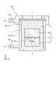
- FIG. 1 is a schematic cross-sectional view of a contactless communication medium according to an embodiment.
- FIG. 2 is a schematic cross-sectional view of the housing according to the embodiment.
- FIG. 3 is a schematic plan view of the housing according to the embodiment.
- FIG. 4 is a schematic cross-sectional view of a fixture according to the embodiment.
- FIG. 5 is a schematic bottom view of the fixture according to the embodiment.
- 6 is a schematic enlarged view showing an example of the VI portion shown in FIG. 1.
- FIG. FIG. 7 is a schematic enlarged view showing another example of the VI section shown in FIG.
- FIG. 8 is a schematic enlarged cross-sectional view of a contactless communication medium according to the first modified example.
- FIG. 9 is a schematic enlarged cross-sectional view of a contactless communication medium according to a second modification.
- FIG. 10 is a schematic enlarged cross-sectional view of a contactless communication medium according to a third modified example.
- FIG. 11 is a schematic enlarged cross-sectional view of a contactless communication medium according to a fourth modification.
- FIG. 12 is a schematic enlarged cross-sectional view of a contactless communication medium according to a fifth modification.
- FIG. 13 is a schematic enlarged cross-sectional view of a contactless communication medium according to a sixth modification.
- FIG. 14 is a schematic enlarged cross-sectional view of a contactless communication medium according to a seventh modification.
- FIG. 1 A form for implementing a contactless communication medium according to the present disclosure (hereinafter referred to as "embodiment”) will be described in detail below with reference to the drawings. Note that this embodiment does not limit the contactless communication medium according to the present disclosure. Further, each embodiment can be appropriately combined within a range that does not contradict the processing contents. Also, in each of the following embodiments, the same parts are denoted by the same reference numerals, and overlapping descriptions are omitted.
- the conventional technology described above has room for further improvement in terms of suppressing the intrusion of liquid or gas from the outside. Therefore, it is expected to provide a non-contact communication medium capable of suppressing intrusion of liquid or gas from the outside.
- FIG. 1 is a schematic cross-sectional view of a contactless communication medium according to an embodiment.
- the non-contact communication medium 100 has an electronic component 1, a housing 3, a lid 4, and fixtures 5.
- the electronic component 1 is housed inside the housing 3 .
- Electronic component 1 may be surrounded by heat insulating material 6, for example.
- the electronic component 1 may be, for example, an RFID tag.
- An electronic component 1 as an RFID has an antenna for contactless communication, an IC chip for contactless communication via this antenna, and identification information on a substrate made of, for example, LTCC (Low Temperature Co-fired Ceramics). and a stored memory.
- the electronic component 1 as RFID can transmit identification information stored in a memory to an external device (for example, an RFID reader) by non-contact communication using electromagnetic induction, radio waves, or the like.
- the non-contact communication medium 100 according to the embodiment is used in a high-temperature environment exceeding the heat-resistant temperature of the electronic component 1, for example.
- the non-contact communication medium 100 according to the embodiment is attached to a component to be plated and immersed in the plating solution together with this component.
- the temperature of the plating solution for hot-dip galvanizing is, for example, 75°C to 500°C.
- the non-contact communication medium 100 according to the embodiment may be treated with acidic chemicals or alkaline chemicals along with the components.
- the contactless communication medium 100 according to the embodiment may be used in an acid/alkali environment that exceeds the chemical resistance of the electronic component 1 .
- the non-contact communication medium 100 may have a heat insulating material 6 that protects the electronic component 1 from a high-temperature environment and an acid/alkali environment, and a protective body 2 having a storage space 25 .
- Electronic component 1 may be positioned in storage space 25 of protector 2 having storage space 25 .
- a heat insulating material may be arranged in the storage space 25 as well.
- the non-contact communication medium 100 includes the housing 3, the lid 4, and the fixture. 5 may be used to seal the protector 2 .
- the protector 2 may have the first base material 21 and the second base material 22 and the adhesive layer 23 .
- the first base material 21 and the second base material 22 may be bonded via an adhesive layer 23 .
- the first base material 21 and the second base material 22 may have, for example, a cylindrical shape. Specifically, the first base material 21 and the second base material 22 have two flat surfaces (upper end surface and lower end surface) that are circular in plan view, and a curved surface (peripheral surface) connecting these two flat surfaces. may have. The upper end surface of the first base material 21 and the lower end surface of the second base material 22 have substantially the same diameter and face each other, and the adhesive layer 23 may be positioned between them.
- the first base material 21 may have a housing recess 251 for housing the electronic component 1 .
- the accommodation recess 251 may open in the center of the upper end surface of the first base material 21 .
- the accommodation space 25 is formed by joining the first base material 21 and the second base material 22 via the adhesive layer 23 to close the accommodation recess 251 .
- the first base material 21 and the second base material 22 may be made of ceramics, for example.
- Cordierite for example, can be used as the ceramics forming the first base material 21 and the second base material 22 . Since cordierite has a small thermal expansion coefficient, it is excellent in thermal shock resistance. Thus, by using cordierite, the electronic component 1 can be appropriately protected from a high-temperature environment.
- the adhesive layer 23 may be positioned between the upper end surface of the first base material 21 and the lower end surface of the second base material 22, and joins the first base material 21 and the second base material 22. good too.
- the adhesive layer 23 only needs to have heat resistance enough to withstand the usage environment of the non-contact communication medium 100 .
- an adhesive layer 23 for example, an inorganic adhesive can be used.
- the ceramics forming the first base material 21 and the second base material 22 are not necessarily cordierite.
- ceramics constituting the first base material 21 and the second base material 22 are Al 2 O 3 (alumina), Si 3 N 4 (silicon nitride), SiC (silicon carbide), Al 2 TiO 5 (aluminum titanate ).
- the ceramics forming the first base material 21 and the second base material 22 may be crystallized glass such as Li 2 O—Al 2 O 3 —SiO 2 .
- the first base material 21 and the second base material 22 do not necessarily have to be made of ceramics.
- the first base material 21 and the second base material 22 may be made of heat-resistant resin.
- the heat-resistant resin constituting the first base material 21 and the second base material 22 for example, PEEK (polyetheretherketone), PBO (polyparaphenylenebenzobisoxazole), and PBI (polybenzimidazole) can be used.
- the first base material 21 and the second base material 22 may have at least heat resistance and radio wave transparency.
- the structure of the protective body 2 is not limited to the illustrated one, and any structure may be used as long as it is made of a member having heat resistance and radio wave permeability and has a space for accommodating the electronic component 1 inside. good.
- the protective body 2 may be a cylindrical body without a bottom or a lid. In that case, the electronic component 1 may be wrapped with, for example, rock wool and fixed in the protector 2 .
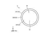
- FIG. 2 is a schematic cross-sectional view of the housing 3 according to the embodiment.
- FIG. 3 is a schematic plan view of the housing 3 according to the embodiment.
- the housing 3 is a cylindrical member with a bottom.
- the housing 3 has a bottom portion 31 that is circular in plan view, and side wall portions 32 that extend from the periphery of the bottom portion 31 perpendicularly to the bottom portion 31 (vertically upward in FIG. 2). good.
- the shape of the side wall portion 32 may be annular in plan view. That is, the side wall portion 32 may have an outer peripheral surface 321 that is circular in plan view and an inner peripheral surface 322 that is circular in plan view.
- Upper end surface 323 of side wall portion 32 may be, for example, a flat surface.
- the housing 3 has an opening 33 on the upper end side, that is, on the opposite side of the bottom portion 31 .
- the opening 33 may have a circular shape in a plan view, and may allow the electronic component 1 to pass therethrough.
- the housing 3 may have a size that allows the protector 2 to pass through.
- the housing 3 may have a flange portion (not shown) located on the upper side of the housing 3 and outside the side wall portion 32 .
- the housing 3 has an opening 33 through which the electronic component 1 can be inserted, and the position facing the opening 33 is closed by the bottom portion 31 .
- the housing 3 may be made of metal, for example.
- the housing 3 made of metal is superior in thermal shock resistance to that made of ceramic.
- Stainless steel, titanium, and the like, for example, can be used as the metal forming the housing 3 .
- Stainless steel and titanium are suitable for use in the plating process in that the plating does not adhere easily.
- the protector 2 may be positioned inside the housing 3, and the heat insulating material 6 may be positioned.
- a heat insulating material 6 may be filled between the protector 2 and the housing 3 .
- the heat insulating material 6 has heat resistance and radio wave transparency.
- heat insulating material 6 for example, rock wool, glass wool, PBO, PBI, cellulose fiber, ceramic powder, or the like may be used.
- the lid 4 is a member that covers the opening 33 of the housing 3 and may be detachable from the housing 3 .
- the lid 4 may be a plate-like member that is circular in plan view.
- the outer diameter of the lid 4 may be larger than the inner diameter of the housing 3 and smaller than the outer diameter of the housing 3 .
- the lid body 4 is in contact with the upper end surface 323 (see FIG. 2) of the housing 3 at its outer peripheral portion.
- the lid 4 has radio wave transparency higher than that of the housing 3 .
- the lid body 4 can be made of ceramics or heat-resistant resin, for example.
- ceramics constituting the lid 4 for example, in addition to cordierite, Al 2 O 3 , Si 3 N 4 , SiC, Al 2 TiO 5 , Li 2 O—Al 2 O 3 —SiO 2 may be used.
- the heat-resistant resin forming the lid 4 for example, PEEK, PBO, PBI, or the like may be used.
- the fixture 5 is a member that fixes the lid 4 to the housing 3 .
- the fixture 5 has an exposure opening 512 through which a portion of the lid 4 is exposed so that contactless communication between the electronic component 1 and the outside is not hindered (see FIG. 1). Non-contact communication between the electronic component 1 and the outside is performed through such an exposure port 512 .
- Protective body 2, heat insulating material 6, and lid 4 located between electronic component 1 and exposure opening 512 all have radio wave permeability, and therefore do not interfere with non-contact communication between electronic component 1 and the outside.
- the fixture 5 may be made of metal, for example.
- the metal forming the fixture 5 may be stainless steel, titanium, or the like, for example.
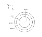
- FIG. 4 is a schematic cross-sectional view of the fixture 5 according to the embodiment.
- FIG. 5 is a schematic bottom view of the fixture 5 according to the embodiment.
- the fixture 5 may be a cap-shaped member that covers the upper portion of the housing 3.
- the fixture 5 includes a ceiling portion 51 that is circular in plan view, and a cylindrical side wall portion 52 that extends from the periphery of the ceiling portion 51 perpendicularly (vertically downward in FIG. 4) to the ceiling portion 51.
- the fixture 5 may be disk-shaped with the exposure opening 512 without the side wall portion 52 .
- the flange portion of the housing 3 and the fixture 5 may be arranged so as to overlap vertically.
- the ceiling part 51 has a ceiling surface 511 facing the lid body 4 . Further, the above-described exposure opening 512 may be positioned at the center of the ceiling portion 51 .
- the side wall portion 52 has an inner peripheral surface 521 that contacts the outer peripheral surface 321 of the housing 3 .
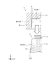
- FIG. 6 is a schematic enlarged view showing an example of the VI portion shown in FIG. 1.
- the housing 3 may have a spiral first groove 325 on the outer peripheral surface 321 of the side wall 32 .
- the fixture 5 may have a spiral second groove portion 523 that screws together with the first groove portion 325 of the housing 3 on the inner peripheral surface 521 of the side wall portion 32 .
- the fixture 5 is fixed to the housing 3 by screwing the first groove portion 325 and the second groove portion 523 together.
- the lid 4 positioned between the housing 3 and the fixture 5 is fixed to the housing 3 so as to be sandwiched between the housing 3 and the fixture 5 .
- the fixture 5 can be removed from the housing 3 . Therefore, of the housing 3 and the fixture 5, for example, when the fixture 5 is damaged, by replacing the fixture 5 with a new one, the undamaged housing 3 can be used continuously. . The same is true when the housing 3 is damaged. Moreover, it is possible to replace not only the housing 3 and the fixture 5, but also the protector 2, the lid 4, and the heat insulating material 6. FIG.
- FIG. 7 is a schematic enlarged view showing another example of the VI section shown in FIG.
- the inner peripheral surface 521 of the side wall portion 52 of the fixture 5 is the first in the direction in which the ceiling surface 511 of the ceiling portion 51 approaches the lid 4 (vertically downward in FIG. 7 ). You may incline by inclination-angle (theta)1. Further, the outer peripheral surface 321 of the housing 3 may be inclined at a second inclination angle ⁇ 2 larger than the first inclination angle ⁇ 1 with respect to the direction in which the ceiling surface 511 of the ceiling portion 51 approaches the lid body 4 .
- the fixture 5 by press-fitting the fixture 5 into the housing 3, the outer peripheral surface 321 of the housing 3 and the inner peripheral surface 521 of the fixture 5 are plastically deformed, and the housing 3 and the fixture 5 are physically separated. integrally. Thereby, the fixture 5 is fixed to the housing 3 .
- the lid 4 positioned between the housing 3 and the fixture 5 is fixed to the housing 3 so as to be sandwiched between the housing 3 and the fixture 5 .
- the lid 4 can be fixed to the housing 3 with a relatively simple structure.
- the non-contact communication medium 100 according to the embodiment has the cylindrical housing 3 with a bottom.
- the housing 3 according to the embodiment has a single opening 33 .
- Such housing 3 has fewer places where liquid or gas enters, compared to the case where both ends are open like the metal case described in Patent Document 1, for example. Therefore, according to the non-contact communication medium 100 according to the embodiment, it is possible to prevent liquid or gas from entering the housing 3 from the outside. Further, by providing the fixing member 5 with the exposure opening 512 , the cover 4 can be fixed to the housing 3 while allowing transmission and reception of radio waves through the cover 4 between the electronic component 1 and the outside.
- cordierite powder and sintering aid powder are prepared.
- Sintering aids are, for example, rare earth oxides (yttrium oxide, cerium oxide, etc.), alkali metal oxides (lithium oxide, sodium oxide, etc.), alkaline earth metals (calcium oxide).
- a mixture of magnesium oxide, aluminum oxide, and silicon oxide at a desired cordierite composition ratio may be used.
- the prepared powder is put into a vibration mill together with water as a solvent, and pulverized and mixed to obtain a raw material.
- organic ingredients such as a binder, a plasticizer, and a release agent are added to the raw material obtained by pulverizing and mixing, and then the mixture is stirred to prepare a slurry.
- Ceramic granules are prepared by spray-drying using
- powder press molding is performed on the produced ceramic granules to obtain a molded body of the first base material 21, the second base material 22 and the lid body 4.
- the compact is degreased by heat treatment in an air atmosphere, a vacuum atmosphere, or a nitrogen gas atmosphere, and then the compact is fired to obtain the first base material 21 and the second base material 22. and the lid 4 is obtained.
- the first base material 21 and the second base material 22 are bonded using an adhesive.
- the protector 2 is accommodated inside the housing 3 and the heat insulating material 6 is filled.
- the protector 2 is placed in the center of the inside of the housing 3, and the remaining gap is filled with the heat insulating material 6. should be filled with By preventing direct contact between the protector 2 and the housing 3 in this manner, heat transfer to the electronic component 1 can be suppressed more reliably.
- the opening 33 of the housing 3 is closed with the lid 4 by placing the lid 4 on the upper end surface 323 of the housing 3 .
- the lid 4 is fixed to the housing 3 with the fixture 5 .
- the lid 4 is fixed to the housing 3 by screwing the second groove 523 of the fixture 5 into the first groove 325 of the housing 3 .
- the lid 4 is fixed to the housing 3 by press-fitting the fixture 5 into the housing 3 .
- the contactless communication medium 100 is obtained.
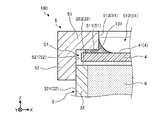
- FIG. 8 is a schematic enlarged cross-sectional view of the contactless communication medium 100 according to the first modified example.
- the non-contact communication medium 100 may have a first sealing portion 101 between the ceiling surface 511 of the fixture 5 and the upper surface 41 of the lid 4 .
- the first sealing portion 101 for example, glass paste, brazing material, heat-resistant resin, or the like can be used.
- the first sealing portion 101 is positioned over the entire circumference of the opening 33 . That is, the first sealing portion 101 seals between the ceiling surface 511 of the fixture 5 and the upper surface 41 of the lid 4 over the entire circumference of the opening 33 .
- the lid 4 may be joined to the ceiling surface 511 via the first sealing portion 101 while being separated from the ceiling surface 511 of the fixture 5 .
- the lid 4 and the fixture 5 By separating the lid 4 and the fixture 5 in this way, the stress caused by the difference in thermal expansion coefficient between the lid 4 and the fixture 5 can be alleviated. Therefore, the thermal cycle resistance of the non-contact communication medium 100 can be improved.
- the lid 4 may be joined to the ceiling surface 511 of the fixture 5 via the first sealing portion 101 while being separated from the housing 3 .
- the lid 4 and the housing 3 By separating the lid 4 and the housing 3 in this way, the stress caused by the difference in thermal expansion coefficient between the lid 4 and the housing 3 can be alleviated. Therefore, the thermal cycle resistance of the non-contact communication medium 100 can be improved.
- the non-contact communication medium 100 may have a space S1 between the side wall portion 52 of the fixture 5 and the lid 4. As described above, the space S1 is positioned in the middle of the path from between the ceiling surface 511 of the fixture 5 and the upper surface 41 of the lid body 4 to the inside of the housing 3. Even if liquid enters through the gap between the ceiling surface 511 and the first sealing portion 101 or the gap between the upper surface 41 of the lid 4 and the first sealing portion 101, the liquid tends to remain in the gap due to capillary action. It is difficult for liquid to enter the inside of the housing 3. Therefore, it is possible to more reliably prevent liquid from entering the housing 3 from the outside.
- the first sealing portion 101 may protrude into the exposure opening 512 from between the ceiling surface 511 of the fixture 5 and the upper surface 41 of the lid 4 .
- part of the first sealing portion 101 is formed on the inner peripheral surface 513 of the ceiling portion 51 corresponding to the peripheral surface of the exposure opening 512 and the portion of the upper surface 41 of the lid 4 exposed from the exposure opening 512 . It may be located in a straddling region. Thereby, the bonding strength between the lid 4 and the fixture 5 can be increased. Moreover, the sealing performance between the upper surface 41 of the lid 4 and the ceiling surface 511 of the fixture 5 can be enhanced.
- a portion of the first sealing portion 101 described above, that is, a portion protruding into the exposure opening 512 may have a meniscus shape.
- the first sealing portion 101 protruding into the exposure opening 512 may have a concave curved surface.
- the ceiling surface 511 of the fixture 5 and the lid 4 are heated by heating the active metal brazing material to a predetermined temperature (for example, a temperature of 600° C. or higher).
- a predetermined temperature for example, a temperature of 600° C. or higher.
- the fixture 5 is fixed to the housing 3 containing the electronic component 1 , the protector 2 and the heat insulating material 6 .
- the lid 4 and the fixture 5 are joined in advance by the first sealing part 101, and then the housing 3 and the fixture 5 are fixed, so that the first sealing part 101 is formed. It is possible to prevent the electronic component 1 from being damaged by high temperature during formation.
- FIG. 9 is a schematic enlarged cross-sectional view of the contactless communication medium 100 according to the second modification.
- a second sealing portion 102 may be provided between the lower surface 42 of the lid 4 and the housing 3 .
- an annular gasket made of heat-resistant resin can be used as the second sealing portion 102.
- the second sealing portion 102 closes the gap between the lower surface 42 of the lid 4 and the upper end surface 323 of the housing 3 by being sandwiched between the lower surface 42 of the lid 4 and the upper end surface 323 of the housing 3 .
- the inside of the housing 3 can be prevented from entering from the outside. Penetration of liquids or gases can be further suppressed.
- a corner portion 327 between the upper end surface 323 and the inner peripheral surface 322 of the housing 3 may bite into the second sealing portion 102 .
- the second sealing portion 102 may be in contact with both the upper end surface 323 and the inner peripheral surface 322 of the housing 3 .
- FIG. 9 shows an example in which not only the second sealing portion 102 but also the first sealing portion 101 is an annular gasket made of heat-resistant resin.
- the first sealing portion 101 may be in contact with both the inner peripheral surface 513 and the upper surface 41 of the ceiling portion 51 of the fixture 5 . With such a configuration, it is possible to more reliably prevent liquid or gas from entering the housing 3 .
- FIG. 10 is a schematic enlarged cross-sectional view of a contactless communication medium 100 according to a third modified example.
- the contactless communication medium 100 may have a space S2 between the second sealing portion 102 and the heat insulating material 6.
- FIG. 10 shows that the contactless communication medium 100 may have a space S2 between the second sealing portion 102 and the heat insulating material 6.
- FIG. 11 is a schematic enlarged cross-sectional view of a contactless communication medium 100 according to a fourth modification.
- the contactless communication medium 100 may have an inner lid 8 between the space S2 and the heat insulating material 6.
- the inner lid 8 has radio wave transparency higher than that of the housing 3 .
- the inner lid 8 can be made of ceramics or heat-resistant resin.
- ceramics constituting the inner lid 8 in addition to cordierite, for example, Al 2 O 3 , Si 3 N 4 , SiC, Al 2 TiO 5 , Li 2 O—Al 2 O 3 —SiO 2 and the like can be used.
- the heat-resistant resin forming the inner lid 8 for example, PEEK, PBO, or PBI can be used.
- the non-contact communication medium 100 may have a third sealing portion 103 between the inner peripheral surface 322 of the housing 3 and the inner lid 8 .
- the third sealing portion 103 has an annular shape.
- the outer diameter of the third sealing portion 103 is larger than the outer diameter of the inner lid 8 .
- the inner diameter of the third sealing portion 103 is smaller than the outer diameter of the inner lid 8 .
- the third sealing portion 103 is made of heat-resistant resin, for example.
- the heat-resistant resin forming the third sealing portion 103 for example, PEEK, PBO, PBI, or the like can be used.
- FIG. 12 is a schematic enlarged cross-sectional view of the contactless communication medium 100 according to the fifth modification.
- the non-contact communication medium 100 is fixed in the direction in which the end surface 522 of the side wall portion 52, more specifically, the ceiling surface 511 of the fixture 5 approaches the lid 4 (vertically downward in FIG. 12).
- a fourth sealing portion 104 may be provided in a region spanning the end surface 522 of the tool 5 and the outer peripheral surface 321 of the housing 3 .
- the fourth sealing portion 104 is located in the above region over the entire circumference of the outer peripheral surface 321 of the housing 3 .
- the fourth sealing portion 104 for example, glass paste, brazing material, heat-resistant resin, inorganic adhesive, or the like can be used.
- the heat-resistant resin for example, polyimide resin or polybenzimidazole resin can be used. Among these resins, it is desirable to use a thermosetting polybenzimidazole resin.
- inorganic adhesives include magnesium silicate and sodium silicate.
- the fourth sealing portion 104 may be a welded portion between the housing 3 and the fixture 5 . The welded portion is a portion where the housing 3 and the fixture 5 are melted and integrated by welding.
- the fourth sealing portion 104 may be arranged around the side wall portion 32 of the housing 3 . Also, the fourth sealing portion 104 may be positioned on a part of the side wall portion 32 of the housing 3 .
- part of the fourth sealing portion 104 is located between the outer peripheral surface 321 of the side wall portion 32 of the housing 3 and the inner peripheral surface 521 of the side wall portion 52 of the fixture 5.
- the non-contact communication medium 100 has a fifth sealing portion located only between the outer peripheral surface 321 of the side wall portion 32 of the housing 3 and the inner peripheral surface 521 of the side wall portion 52 of the fixture 5. may have.
- FIG. 13 is a schematic enlarged cross-sectional view of the contactless communication medium 100 according to the sixth modification.
- the housing 3 may have a first protrusion 35 that protrudes outward from the outer peripheral surface 321 .
- the first projecting portion 35 has a first through hole 351 passing through the first projecting portion 35 .
- the fixture 5 may have a second protrusion 55 that protrudes outward from the outer peripheral surface 525 .
- the second projecting portion 55 has a second through hole 551 passing through the second projecting portion 55 .
- the contactless communication medium 100 may have the first through hole 351 located in the housing 3 and the second through hole 551 located in the fixture 5 .
- wires can be inserted through the first through-hole 351 and the second through-hole 551, and the contactless communication medium 100 can be attached to the article to be managed through the wires.
- the non-contact communication medium 100 may be configured to have only one of the first projecting portion 35 and the second projecting portion 55 . In other words, the non-contact communication medium 100 may have only one of the first through hole 351 and the second through hole 551 .
- FIG. 14 is a schematic enlarged cross-sectional view of a contactless communication medium 100 according to a seventh modification.
- the non-contact communication medium 100 may fasten the housing 3 and fixture 5 with bolts 201 and nuts 202 .
- the housing 3 may have multiple first through holes 351 .
- FIG. 14 shows an example in which a plurality of first through-holes 351 are positioned in the flange-like first projecting portion 35 .
- the structure is not limited to this, and the housing 3 may have a plurality of first protrusions 35 and each first protrusion 35 may have a first through hole 351 .
- the fixture 5 may have a plurality of second through holes 551 .
- FIG. 14 shows an example in which a plurality of second through holes 551 are positioned in the flange-shaped second projecting portion 55 .
- the fixture 5 may have a configuration in which a plurality of second projecting portions 55 are provided and each of the second projecting portions 55 is provided with a second through hole 551 .
- the fixture 5 can be fixed to the housing 3 by inserting the bolt 201 through the first through hole 351 and the second through hole 551 and tightening it with the nut 202. can. Further, by fixing the fixture 5 to the housing 3 , the lid 4 located between the housing 3 and the fixture 5 can be fixed to the housing 3 .
- Electronic components are not limited to RFID tags, and may be other electronic components as long as they perform contactless communication.
- the electronic component may be a sensor with contactless communication capabilities.
- the sensor may be a sensor that measures the process environment of the monitored component, for example a temperature sensor.
- the parts to which contactless communication media are attached are not limited to parts that are plated.
- the contactless communication medium may be attached to a component such as a billet produced in a foundry of metallic materials.
- the non-contact communication medium (as an example, the non-contact communication medium 100) according to the embodiment includes an electronic component (as an example, the electronic component 1), a housing (as an example, a housing 3), It has a lid (a lid 4 as an example) and a fixture (a fixture 5 as an example).
- the electronic component performs contactless communication.
- the housing has an opening (for example, an opening 33) through which electronic components can be inserted, and the position facing the opening is closed.
- the lid has higher radio wave transmittance than the housing and covers the opening.
- the fixture fixes the lid to the housing while partially exposing the lid.
- the contactless communication medium according to the embodiment it is possible to suppress the invasion of liquid or gas from the outside.
Abstract
本開示による非接触通信媒体(100)は、電子部品(1)と、筐体(3)と、蓋体(4)と、固定具(5)とを有する。電子部品(1)は、非接触通信を行う。筐体(4)は、電子部品(1)を挿通可能な開口(33)を有し、開口(33)と対向する位置が塞がれている。蓋体(4)は、筐体(3)よりも電波透過性が高く、開口(33)を覆っている。固定具(5)は、蓋体(4)の一部を露出させつつ、蓋体(4)を筐体(3)に固定する。
Description
本開示は、非接触通信媒体に関する。
従来、RFID(Radio Frequency Identifier)タグ等を用いた物品管理が行われている。
特許文献1には、溶融亜鉛めっき処理等の高温環境下でのRFIDタグの使用を可能にするために、RFIDタグを覆う断熱材が内部に充填された金属ケースからなる収容体が開示されている。
金属ケースは、両端が開放された円筒形状を有している。金属ケースが有する2つの開口部のうち、一方の開口部は、金属製の蓋体によって塞がれている。金属製の蓋体は、金属ケースに対して着脱自在であり、内部の断熱材を交換する際に金属ケースから取り外される。また、金属ケースの他方の開口部は、RFIDタグと外部との非接触通信(電波の送受信)が妨げられないように、内部の断熱材が露出した状態となっている。
本開示の一態様による非接触通信媒体は、電子部品と、筐体と、蓋体と、固定具とを有する。電子部品は、非接触通信を行う。筐体は、電子部品を挿通可能な開口を有し、開口と対向する位置が塞がれている。蓋体は、筐体よりも電波透過性が高く、開口を覆っている。固定具は、蓋体の一部を露出させつつ、蓋体を筐体に固定する。
以下に、本開示による非接触通信媒体を実施するための形態(以下、「実施形態」と記載する)について図面を参照しつつ詳細に説明する。なお、この実施形態により本開示による非接触通信媒体が限定されるものではない。また、各実施形態は、処理内容を矛盾させない範囲で適宜組み合わせることが可能である。また、以下の各実施形態において同一の部位には同一の符号を付し、重複する説明は省略される。
また、以下に示す実施形態では、「一定」、「直交」、「垂直」あるいは「平行」といった表現が用いられる場合があるが、これらの表現は、厳密に「一定」、「直交」、「垂直」あるいは「平行」であることを要しない。すなわち、上記した各表現は、たとえば製造精度、設置精度などのずれを許容するものとする。
また、以下で参照する各図は、説明の便宜上の模式的なものである。したがって、細部は省略されることがあり、また、寸法比率は必ずしも現実のものとは一致していない。
また、以下参照する各図面では、説明を分かりやすくするために、互いに直交するX軸方向、Y軸方向およびZ軸方向を規定し、Z軸正方向を鉛直上向き方向とする直交座標系を示す場合がある。
上述した従来技術では、外部からの液体または気体の侵入を抑制するという点でさらなる改善の余地がある。そこで、外部からの液体または気体の侵入を抑制することができる非接触通信媒体の提供が期待されている。
<非接触通信媒体の全体構成>
まず、実施形態に係る非接触通信媒体の全体構成について図1を参照して説明する。図1は、実施形態に係る非接触通信媒体の模式的な断面図である。
まず、実施形態に係る非接触通信媒体の全体構成について図1を参照して説明する。図1は、実施形態に係る非接触通信媒体の模式的な断面図である。
図1に示すように、実施形態に係る非接触通信媒体100は、電子部品1と、筐体3と、蓋体4と、固定具5と、を有する。電子部品1は、筐体3の内部に収容されている。電子部品1は、たとえば、断熱材6に囲まれていてもよい。
電子部品1は、たとえばRFIDタグであってもよい。RFIDとしての電子部品1は、たとえばLTCC(Low Temperature Co-fired Ceramics)等からなる基板上に、非接触通信用のアンテナと、このアンテナを介して非接触通信を行うICチップと、識別情報を記憶したメモリとを有する。RFIDとしての電子部品1は、電磁誘導、電波等を用いた非接触通信により、メモリに記憶された識別情報を外部機器(たとえば、RFIDリーダー)に送信することができる。
一例として、実施形態に係る非接触通信媒体100は、たとえば、電子部品1の耐熱温度を超える高温環境下で使用される。たとえば、実施形態に係る非接触通信媒体100は、めっき処理される部品に取り付けられ、この部品とともにめっき液に浸漬される。溶融亜鉛めっき等のめっき液の温度は、たとえば、75℃~500℃である。
また、実施形態に係る非接触通信媒体100は、部品とともに酸性の薬品やアルカリ性の薬品によって処理される場合がある。このように、実施形態に係る非接触通信媒体100は、電子部品1の耐薬品性を超える酸・アルカリ環境下において使用されることもある。
そこで、実施形態に係る非接触通信媒体100は、電子部品1を高温環境、酸・アルカリ環境から保護する断熱材6や、収納空間25を有する保護体2を有していてもよい。電子部品1は、収納空間25を有する保護体2の収納空間25に位置していてもよい。なお、収納空間25にも断熱材が配置されていてもよい。
セラミックスまたは耐熱樹脂で構成される保護体2に、繰り返し使用する上での耐久性に課題がある場合には、実施形態に係る非接触通信媒体100は、筐体3、蓋体4および固定具5を用いて保護体2を封止してもよい。
保護体2は、第1基材21および第2基材22と、接着層23とを有していてもよい。第1基材21と第2基材22とは、接着層23を介して接合されていてもよい。
第1基材21および第2基材22は、たとえば円柱形状を有していてもよい。具体的には、第1基材21および第2基材22は、平面視円形の2つの平坦面(上端面および下端面)を有するとともに、これら2つの平坦面を繋ぐ曲面(外周面)を有していてもよい。第1基材21の上端面と第2基材22の下端面とは、略同径で互いに対向しており、これらの間に接着層23が位置していてもよい。
第1基材21は、電子部品1を収容する収容凹部251を有していてもよい。収容凹部251は、第1基材21の上端面の中央部に開口していてもよい。たとえば、第1基材21と第2基材22とが接着層23を介して接合されて収容凹部251が塞がれることで、収容空間25が形成される。
第1基材21および第2基材22は、たとえばセラミックスからなっていてもよい。第1基材21および第2基材22を構成するセラミックスとしては、たとえばコージェライトを用いることができる。コージェライトは、熱膨張係数が小さいことから、耐熱衝撃性に優れており、また、熱伝導率が低いことから、電子部品1に熱を伝え難い。このように、コージェライトを使用することで、電子部品1を高温環境から適切に保護することができる。
接着層23は、第1基材21の上端面と第2基材22の下端面との間に位置していてもよく、第1基材21と第2基材22とを接合していてもよい。接着層23は、非接触通信媒体100の使用環境に耐え得る耐熱性を有していればよい。このような接着層23としては、たとえば無機系の接着剤を用いることができる。
なお、第1基材21および第2基材22を構成するセラミックスは、必ずしも、コージェライトであることを要しない。たとえば、第1基材21および第2基材22を構成するセラミックスは、Al2O3(アルミナ)、Si3N4(窒化ケイ素)、SiC(炭化ケイ素)、Al2TiO5(チタン酸アルミニウム)であってもよい。また、第1基材21および第2基材22を構成するセラミックスは、Li2O-Al2O3-SiO2等の結晶化ガラスであってもよい。
また、第1基材21および第2基材22は、必ずしも、セラミックスで形成されることを要しない。たとえば、第1基材21および第2基材22は、耐熱性樹脂で形成されてもよい。第1基材21および第2基材22を構成する耐熱性樹脂としては、たとえばPEEK(ポリエーテルエーテルケトン)、PBO(ポリパラフェニレンベンゾビスオキサゾール)、PBI(ポリベンゾイミダゾール)を用いることができる。第1基材21および第2基材22は、少なくとも耐熱性および電波透過性を有するものであればよい。
保護体2の構成は、図示のものに限定されず、耐熱性および電波透過性を有する部材で構成され、内部に電子部品1の収容空間を有するものであれば、いずれの構成であってもよい。また、保護体2は、底や蓋のない筒状体であってもよい。その場合には、たとえばロックウールなどで電子部品1を包み、保護体2の中に固定してもよい。
<筐体について>
図2は、実施形態に係る筐体3の模式的な断面図である。また、図3は、実施形態に係る筐体3の模式的な平面図である。
図2は、実施形態に係る筐体3の模式的な断面図である。また、図3は、実施形態に係る筐体3の模式的な平面図である。
図2および図3に示すように、筐体3は、有底筒状の部材である。具体的には、筐体3は、平面視円形の底部31と、底部31の周縁部から底部31に対して垂直に(図2では鉛直上方に)延びる側壁部32とを有していてもよい。側壁部32の形状は、平面視において環状であってもよい。すなわち、側壁部32は、平面視円形状の外周面321と平面視円形状の内周面322とを有していてもよい。側壁部32の上端面323は、たとえば平坦面であってもよい。
かかる筐体3は、上端側、すなわち、底部31の反対側に開口33を有する。開口33は、平面視円形状であってもよく、電子部品1を挿通可能であってもよい。また、電子部品1が保護体2に収容されている場合には、筐体3は、保護体2を挿通可能な大きさを有していてもよい。また、筐体3は、筐体3の上側であり、側壁部32の外側に位置する鍔部(図示せず)を有していてもよい。
このように、筐体3は、電子部品1を挿通可能な開口33を有しており、開口33と対向する位置が底部31によって塞がれている。
筐体3は、たとえば金属で形成されていてもよい。金属で形成された筐体3は、セラミック製の場合よりも耐熱衝撃性に優れる。筐体3を構成する金属としては、たとえばステンレス鋼およびチタン等を用いることができる。ステンレス鋼およびチタンは、めっきが付着しにくいという点で、めっき処理での使用に適している。
図1に示すように、筐体3の内部に、保護体2が位置していてもよく、断熱材6が位置していてもよい。断熱材6は、保護体2と筐体3との間に充填されていてもよい。断熱材6は、耐熱性および電波透過性を有する。このような断熱材6としては、たとえば、ロックウール、グラスウール、PBO、PBI、セルロースファイバーおよびセラミックス粉末等を用いてもよい。
<蓋体について>
蓋体4は、筐体3の開口33を覆う部材であり、筐体3に対して着脱可能であってもよい。蓋体4は、平面視円形状の板状部材であってもよい。蓋体4の外径は、筐体3の内径よりも大きく、筐体3の外径よりも小さてもよい。図1に示す例において、蓋体4は、外周部において筐体3の上端面323(図2参照)に当接している。
蓋体4は、筐体3の開口33を覆う部材であり、筐体3に対して着脱可能であってもよい。蓋体4は、平面視円形状の板状部材であってもよい。蓋体4の外径は、筐体3の内径よりも大きく、筐体3の外径よりも小さてもよい。図1に示す例において、蓋体4は、外周部において筐体3の上端面323(図2参照)に当接している。
蓋体4は、筐体3よりも高い電波透過性を有する。このような蓋体4としては、たとえば第1基材21および第2基材22と同様、セラミックスや耐熱性樹脂で形成されうる。蓋体4を構成するセラミックスとしては、たとえばコージェライトの他、Al2O3、Si3N4、SiC、Al2TiO5、Li2O-Al2O3-SiO2等を用いてもよい。また、蓋体4を構成する耐熱性樹脂としては、たとえばPEEK、PBOおよびPBI等を用いてもよい。
<固定具について>
固定具5は、蓋体4を筐体3に固定する部材である。固定具5は、電子部品1と外部との非接触通信が妨げられないように、蓋体4の一部を露出させる露出口512を有している(図1参照)。電子部品1と外部との非接触通信は、かかる露出口512を介して行われる。電子部品1と露出口512との間に位置する保護体2、断熱材6および蓋体4は、いずれも電波透過性を有するため、電子部品1と外部との非接触通信を妨げない。
固定具5は、蓋体4を筐体3に固定する部材である。固定具5は、電子部品1と外部との非接触通信が妨げられないように、蓋体4の一部を露出させる露出口512を有している(図1参照)。電子部品1と外部との非接触通信は、かかる露出口512を介して行われる。電子部品1と露出口512との間に位置する保護体2、断熱材6および蓋体4は、いずれも電波透過性を有するため、電子部品1と外部との非接触通信を妨げない。
固定具5は、たとえば金属で形成されていてもよい。固定具5を構成する金属は、たとえばステンレス鋼およびチタン等であってもよい。
次に、固定具5の具体的な構成について図4および図5を参照して説明する。図4は、実施形態に係る固定具5の模式的な断面図である。また、図5は、実施形態に係る固定具5の模式的な底面図である。
図4および図5に示すように、実施形態に係る固定具5は、筐体3の上部に被さるキャップ状の部材であってもよい。具体的には、固定具5は、平面視円形状の天井部51と、天井部51の周縁部から天井部51に対して垂直に(図4では鉛直下方に)延びる円筒状の側壁部52とを有していてもよい。また、固定具5は側壁部52を有さず、露出口512を有する円盤状であってもよい。固定具5が円盤状である場合には、たとえば、前述した筐体3の鍔部と固定具5とが上下に重なり合うように配置してもよい。
天井部51は、蓋体4と対向する天井面511を有する。また、天井部51の中央には、上述した露出口512が位置していてもよい。側壁部52は、筐体3の外周面321と当接する内周面521を有する。
<蓋体の固定方法について>
次に、固定具5による蓋体4の固定方法の一例について図6を参照して説明する。図6は、図1に示すVI部の一例を示す模式的な拡大図である。
次に、固定具5による蓋体4の固定方法の一例について図6を参照して説明する。図6は、図1に示すVI部の一例を示す模式的な拡大図である。
図6に示すように、筐体3は、側壁部32の外周面321に螺旋状の第1溝部325を有していてもよい。また、固定具5は、側壁部32の内周面521に、筐体3の第1溝部325と螺合する螺旋状の第2溝部523を有してもよい。この場合、第1溝部325と第2溝部523とが螺合することによって固定具5が筐体3に固定される。これに伴い、筐体3と固定具5との間に位置する蓋体4は、筐体3と固定具5とに挟み込まれるようにして筐体3に固定される。
このように、筐体3と固定具5とを螺合により固定することとした場合、固定具5を筐体3から取り外すことができる。このため、筐体3および固定具5のうち、たとえば固定具5が損傷した場合に、固定具5を新品と交換することで、損傷していない筐体3を継続して使用することができる。筐体3が損傷した場合も同様である。また、筐体3や固定具5に限らず、保護体2、蓋体4、断熱材6を交換することも可能である。
図7は、図1に示すVI部の他の一例を示す模式的な拡大図である。図7に示すように、固定具5が有する側壁部52の内周面521は、天井部51の天井面511を蓋体4に接近させる方向(図7では、鉛直下方)に対して第1傾斜角度θ1で傾斜してもよい。また、筐体3の外周面321は、天井部51の天井面511を蓋体4に接近させる方向に対し、第1傾斜角度θ1よりも大きい第2傾斜角度θ2で傾斜していてもよい。
この場合、固定具5を筐体3に対して圧入することで、筐体3の外周面321および固定具5の内周面521が塑性変形して、筐体3と固定具5とが物理的に一体化する。これにより、筐体3に対して固定具5が固定される。これに伴い、筐体3と固定具5との間に位置する蓋体4は、筐体3と固定具5とに挟み込まれるようにして筐体3に固定される。
かかる構成とすることにより、比較的簡易な構造で蓋体4を筐体3に固定することができる。
このように、実施形態に係る非接触通信媒体100は、有底筒状の筐体3を有する。言い換えれば、実施形態に係る筐体3は、単一の開口33を有する。かかる筐体3は、たとえば特許文献1に記載の金属ケースのように両端が開放されている場合と比較して、液体または気体の侵入箇所が少ない。したがって、実施形態に係る非接触通信媒体100によれば、外部から筐体3の内部への液体または気体の侵入を抑制することができる。また、固定具5に露出口512を設けることで、電子部品1と外部との間での蓋体4を介した電波の送受信を可能としつつ、蓋体4を筐体3に固定できる。
<製造方法>
次に、実施形態に係る非接触通信媒体100の製造方法の一例について説明する。ここでは、第1基材21、第2基材22および蓋体4がセラミックスからなる場合の例について説明する。また、ここでは、金属からなる筐体3および固定具5については、予め得られているものとして説明する。
次に、実施形態に係る非接触通信媒体100の製造方法の一例について説明する。ここでは、第1基材21、第2基材22および蓋体4がセラミックスからなる場合の例について説明する。また、ここでは、金属からなる筐体3および固定具5については、予め得られているものとして説明する。
まず、コージェライトの粉末および焼結助剤の粉末を準備する。焼結助剤は、たとえば、希土類酸化物(酸化イットリウム、酸化セリウムなど)、アルカリ金属酸化物(酸化リチウム、酸化ナトリウムなど)、アルカリ土類金属(酸化カルシウム)である。なお、コージェライトの粉末の代わりに、酸化マグネシウム、酸化アルミニウム、酸化珪素を所望のコージェライトの組成比に混合したものを用いてもよい。つづいて、準備した粉末を溶媒である水とともに振動ミルに投入して、粉砕・混合して原料を得る。
つづいて、粉砕・混合して得られた原料に対し、バインダー、可塑剤および離型剤などの有機成分を添加した後、これらを撹拌することによってスラリーを作製し、作製したスラリーをスプレードライヤーを用いて噴霧乾燥することによってセラミックス顆粒を作製する。
つづいて、作製したセラミックス顆粒に対して粉末プレス成形を行って、第1基材21、第2基材22および蓋体4の成形体を得る。
つづいて、大気雰囲気中、真空雰囲気中または窒素ガス雰囲気中にて成形体を熱処理することにより脱脂を行った後、成形体の焼成を行うことにより、第1基材21、第2基材22および蓋体4が得られる。
つづいて、収容凹部251に電子部品1を収容した後、第1基材21と第2基材22とを接着剤を用いて接合する。
つづいて、筐体3の内部に保護体2を収容するとともに断熱材6を充填する。このとき、保護体2と筐体3とが直接触れ合わないように断熱材6を充填することが好ましい。たとえば、まず、筐体3の内部の1/3~1/2程度を断熱材6で満たした後、筐体3の内部の中央に保護体2を載置し、残りの隙間を断熱材6で埋めればよい。このように、保護体2と筐体3とが直接触れ合わないようにすることで、電子部品1への伝熱をより確実に抑制することができる。
つづいて、筐体3の上端面323に蓋体4を載置することにより、筐体3の開口33を蓋体4で塞ぐ。そして、固定具5で蓋体4を筐体3に固定する。たとえば、図6に示す構成の場合、筐体3の第1溝部325に対して固定具5の第2溝部523を螺合させることにより、蓋体4を筐体3に固定する。また、図7に示す構成の場合、筐体3に対して固定具5を圧入することにより、蓋体4を筐体3に固定する。以上により、非接触通信媒体100が得られる。
<第1変形例>
図8は、第1変形例に係る非接触通信媒体100の模式的な拡大断面図である。図8に示すように、非接触通信媒体100は、固定具5の天井面511と蓋体4の上面41との間に第1封止部101を有していてもよい。第1封止部101としては、たとえば、ガラスペースト、ろう材および耐熱性樹脂等を用いることができる。
図8は、第1変形例に係る非接触通信媒体100の模式的な拡大断面図である。図8に示すように、非接触通信媒体100は、固定具5の天井面511と蓋体4の上面41との間に第1封止部101を有していてもよい。第1封止部101としては、たとえば、ガラスペースト、ろう材および耐熱性樹脂等を用いることができる。
第1封止部101は、開口33の全周に亘って位置している。すなわち、第1封止部101は、開口33の全周に亘って固定具5の天井面511と蓋体4の上面41との間を封止している。
このように、液体または気体の侵入箇所となり得る固定具5の天井面511と蓋体4の上面41との隙間を第1封止部101で塞ぐことにより、外部から筐体3の内部への液体または気体の侵入をさらに抑制することができる。
蓋体4は、固定具5の天井面511から離隔した状態で、第1封止部101を介して天井面511に接合されていてもよい。このように、蓋体4と固定具5とを離隔させることで、蓋体4と固定具5との熱膨張係数差によって生じる応力を緩和することができる。したがって、非接触通信媒体100の耐熱サイクル性を向上させることができる。
蓋体4は、筐体3から離隔した状態で、第1封止部101を介して固定具5の天井面511に接合されていてもよい。このように、蓋体4と筐体3とを離隔させることで、蓋体4と筐体3との熱膨張係数差によって生じる応力を緩和することができる。したがって、非接触通信媒体100の耐熱サイクル性を向上させることができる。
非接触通信媒体100は、固定具5の側壁部52と蓋体4との間に空間S1を有していてもよい。このように、固定具5の天井面511と蓋体4の上面41との間から筐体3の内部へ至る侵入経路の途中に空間S1が位置していることで、仮に、固定具5の天井面511と第1封止部101の隙間または蓋体4の上面41と第1封止部101との隙間から液体が侵入したとしても、毛管現象によって液体が上記隙間に留まり易くなるため、筐体3の内部に液体が侵入し難い。したがって、外部から筐体3の内部への液体の侵入をより確実に抑制することができる。
第1封止部101は、固定具5の天井面511と蓋体4の上面41との間から露出口512にはみ出ていてもよい。言い換えれば、第1封止部101の一部は、露出口512の周面に相当する天井部51の内周面513と、蓋体4の上面41のうち露出口512から露出した部分とに跨がる領域に位置していてもよい。これにより、蓋体4と固定具5との接合強度を高めることができる。また、蓋体4の上面41と固定具5の天井面511との間のシール性を高めることができる。
上述した第1封止部101の一部、すなわち、露出口512にはみ出た部分は、メニスカス形状を有していてもよい。具体的には、露出口512にはみ出た第1封止部101は、凹曲面状の表面を有していてもよい。かかる構成とすることにより、表面形状を凸曲面状としたときと比較して、固定具5の内周面513および蓋体4の上面41との接触面積が大きくなるため、蓋体4と固定具5との接合強度を高めることができる。
変形例1に係る非接触通信媒体100を製造する場合、たとえば活性金属ろう材を所定の温度(たとえば、600℃以上の温度)で加熱することにより、固定具5の天井面511と蓋体4の上面41との間に第1封止部101を形成して固定具5と蓋体4とを接合する。その後、電子部品1、保護体2および断熱材6を収容した筐体3に固定具5を固定する。このように、予め蓋体4と固定具5とを第1封止部101で接合したうえで、筐体3と固定具5とを固定するようにすることで、第1封止部101を形成する際の高温によって電子部品1が損傷することを防止することができる。
<第2変形例>
図9は、第2変形例に係る非接触通信媒体100の模式的な拡大断面図である。図9に示すように、蓋体4の下面42と筐体3との間に第2封止部102を有していてもよい。第2封止部102としては、たとえば耐熱性樹脂からなる円環状のガスケットを用いることができる。
図9は、第2変形例に係る非接触通信媒体100の模式的な拡大断面図である。図9に示すように、蓋体4の下面42と筐体3との間に第2封止部102を有していてもよい。第2封止部102としては、たとえば耐熱性樹脂からなる円環状のガスケットを用いることができる。
第2封止部102は、蓋体4の下面42と筐体3の上端面323とに挟み込まれることにより、蓋体4の下面42と筐体3の上端面323との隙間を塞ぐ。このように、液体または気体の侵入箇所となり得る蓋体4の下面42と筐体3の上端面323との隙間を第2封止部102で塞ぐことにより、外部から筐体3の内部への液体または気体の侵入をさらに抑制することができる。
筐体3の上端面323と内周面322との角部327は、第2封止部102に食い込んでいてもよい。言い換えれば、第2封止部102は、筐体3の上端面323と内周面322との両面に接していてもよい。このような構成とすることにより、筐体3の内部への液体または気体の侵入をより確実に抑制することができる。
なお、図9では、第2封止部102だけでなく第1封止部101も耐熱性樹脂からなる円環状のガスケットである場合の例を示している。この場合、図9に示すように、第1封止部101は、固定具5が有する天井部51の内周面513と上面41との両面に接していてもよい。このような構成とすることにより、筐体3の内部への液体または気体の侵入をより確実に抑制することができる。
<第3変形例>
図10は、第3変形例に係る非接触通信媒体100の模式的な拡大断面図である。図10に示すように、非接触通信媒体100は、第2封止部102と断熱材6との間に空間S2を有していてもよい。
図10は、第3変形例に係る非接触通信媒体100の模式的な拡大断面図である。図10に示すように、非接触通信媒体100は、第2封止部102と断熱材6との間に空間S2を有していてもよい。
かかる構成とすることにより、仮に、蓋体4の下面42と第2封止部102との隙間または筐体3と第2封止部102との隙間から液体が侵入したとしても、毛管現象によって液体がかかる隙間に留まり易くなるため、筐体3の内部に液体が侵入し難い。したがって、外部から筐体3の内部への液体の侵入をより確実に抑制することができる。
<第4変形例>
図11は、第4変形例に係る非接触通信媒体100の模式的な拡大断面図である。図11に示すように、非接触通信媒体100は、空間S2と断熱材6との間に中蓋8を有していてもよい。中蓋8は、筐体3よりも高い電波透過性を有する。このような中蓋8としては、たとえば蓋体4と同様、セラミックスや耐熱性樹脂で形成されうる。中蓋8を構成するセラミックスとしては、たとえばコージェライトの他、Al2O3、Si3N4、SiC、Al2TiO5、Li2O-Al2O3-SiO2等を用いることができる。また、中蓋8を構成する耐熱性樹脂としては、たとえばPEEK、PBO、PBIを用いることができる。
図11は、第4変形例に係る非接触通信媒体100の模式的な拡大断面図である。図11に示すように、非接触通信媒体100は、空間S2と断熱材6との間に中蓋8を有していてもよい。中蓋8は、筐体3よりも高い電波透過性を有する。このような中蓋8としては、たとえば蓋体4と同様、セラミックスや耐熱性樹脂で形成されうる。中蓋8を構成するセラミックスとしては、たとえばコージェライトの他、Al2O3、Si3N4、SiC、Al2TiO5、Li2O-Al2O3-SiO2等を用いることができる。また、中蓋8を構成する耐熱性樹脂としては、たとえばPEEK、PBO、PBIを用いることができる。
このように、空間S2と断熱材6との間に中蓋8を設けた場合、仮に、筐体3の内部に液体または気体が侵入したとしても、侵入した液体または気体が断熱材6に接触し難くなる。すなわち、侵入した液体または気体が電子部品1に到達し難くなる。したがって、第4変形例に係る非接触通信媒体100によれば、仮に、筐体3の内部に液体または気体が侵入した場合であっても、電子部品1の損傷を抑制することができる。
また、非接触通信媒体100は、筐体3の内周面322と中蓋8との間に第3封止部103を有していてもよい。第3封止部103は、円環形状を有する。第3封止部103の外径は、中蓋8の外径よりも大きい。また、第3封止部103の内径は、中蓋8の外径よりも小さい。第3封止部103は、たとえば耐熱性樹脂からなる。第3封止部103を構成する耐熱性樹脂としては、たとえばPEEK、PBOおよびPBI等を用いることができる。
このように、筐体3の内周面322と中蓋8との隙間を第3封止部103で塞ぐことにより、仮に、液体または気体が筐体3の内部に侵入したとしても、侵入した液体または気体が電子部品1に到達することを抑制することができる。
<第5変形例>
図12は、第5変形例に係る非接触通信媒体100の模式的な拡大断面図である。図12に示すように、非接触通信媒体100は、側壁部52の端面522、具体的には、固定具5の天井面511を蓋体4に接近させる方向(図12では鉛直下方)における固定具5の端面522と、筐体3の外周面321とに跨がる領域に第4封止部104を有していてもよい。第4封止部104は、筐体3の外周面321の全周に亘って上記領域に位置している。第4封止部104としては、たとえば、ガラスペースト、ろう材、耐熱性樹脂および無機接着剤等を用いることができる。耐熱性樹脂としては、たとえば、ポリイミド樹脂またはポリベンゾイミダゾール樹脂等を用いることができる。これらの樹脂のなかでも、熱硬化性のポリベンゾイミダゾール樹脂を用いることが望ましい。無機接着剤としては、たとえば、マグネシウムケイ酸塩、ナトリウムケイ酸塩等を用いることができる。また、第4封止部104は、筐体3と固定具5との溶接部であってもよい。溶接部とは、筐体3と固定具5とが溶接加工によって溶けて一体化した部分のことである。第4封止部104は、筐体3の側壁部32を1周して配置していてもよい。また、第4封止部104は、筐体3の側壁部32の一部に位置していてもよい。
図12は、第5変形例に係る非接触通信媒体100の模式的な拡大断面図である。図12に示すように、非接触通信媒体100は、側壁部52の端面522、具体的には、固定具5の天井面511を蓋体4に接近させる方向(図12では鉛直下方)における固定具5の端面522と、筐体3の外周面321とに跨がる領域に第4封止部104を有していてもよい。第4封止部104は、筐体3の外周面321の全周に亘って上記領域に位置している。第4封止部104としては、たとえば、ガラスペースト、ろう材、耐熱性樹脂および無機接着剤等を用いることができる。耐熱性樹脂としては、たとえば、ポリイミド樹脂またはポリベンゾイミダゾール樹脂等を用いることができる。これらの樹脂のなかでも、熱硬化性のポリベンゾイミダゾール樹脂を用いることが望ましい。無機接着剤としては、たとえば、マグネシウムケイ酸塩、ナトリウムケイ酸塩等を用いることができる。また、第4封止部104は、筐体3と固定具5との溶接部であってもよい。溶接部とは、筐体3と固定具5とが溶接加工によって溶けて一体化した部分のことである。第4封止部104は、筐体3の側壁部32を1周して配置していてもよい。また、第4封止部104は、筐体3の側壁部32の一部に位置していてもよい。
かかる構成とすることにより、外部から筐体3の内部への液体または気体の侵入を抑制することができる。また、かかる構成とすることにより、筐体3と固定具5との緩みを抑制することができる。
また、図12に示すように、第4封止部104の一部は、筐体3における側壁部32の外周面321と固定具5における側壁部52の内周面521との間に位置していてもよい。かかる構成とすることにより、外部から筐体3の内部への液体または気体の侵入を抑制することができる。また、かかる構成とすることにより、筐体3と固定具5との緩みを抑制することができる。また、図示しないが、非接触通信媒体100は、筐体3における側壁部32の外周面321と固定具5における側壁部52の内周面521との間にのみ位置する第5封止部を有していてもよい。
<第6変形例>
図13は、第6変形例に係る非接触通信媒体100の模式的な拡大断面図である。図13に示すように、筐体3は、外周面321から外方に突出する第1突出部35を有していてもよい。第1突出部35は、第1突出部35を貫通する第1貫通孔351を有する。また、固定具5は、外周面525から外方に突出する第2突出部55を有していてもよい。第2突出部55は、第2突出部55を貫通する第2貫通孔551を有する。
図13は、第6変形例に係る非接触通信媒体100の模式的な拡大断面図である。図13に示すように、筐体3は、外周面321から外方に突出する第1突出部35を有していてもよい。第1突出部35は、第1突出部35を貫通する第1貫通孔351を有する。また、固定具5は、外周面525から外方に突出する第2突出部55を有していてもよい。第2突出部55は、第2突出部55を貫通する第2貫通孔551を有する。
このように、非接触通信媒体100は、筐体3に位置する第1貫通孔351と固定具5に位置する第2貫通孔551とを有していてもよい。この場合、たとえば、第1貫通孔351および第2貫通孔551にワイヤを挿通することができ、かかるワイヤを介して管理対象としての物品に非接触通信媒体100を取り付けることができる。
なお、非接触通信媒体100は、第1突出部35および第2突出部55のうち一方のみを有する構成であってもよい。言い換えれば、非接触通信媒体100は、第1貫通孔351および第2貫通孔551のうち一方のみを有する構成であってもよい。
<第7変形例>
図14は、第7変形例に係る非接触通信媒体100の模式的な拡大断面図である。図14に示すように、非接触通信媒体100は、ボルト201およびナット202によって筐体3と固定具5とを締結してもよい。
図14は、第7変形例に係る非接触通信媒体100の模式的な拡大断面図である。図14に示すように、非接触通信媒体100は、ボルト201およびナット202によって筐体3と固定具5とを締結してもよい。
たとえば、筐体3は、複数の第1貫通孔351を有していてもよい。図14では、フランジ状の第1突出部35に複数の第1貫通孔351が位置している場合の例を示している。これに限らず、筐体3は、複数の第1突出部35を有するとともに、各第1突出部35に第1貫通孔351を有する構成であってもよい。
また、固定具5は、複数の第2貫通孔551を有していてもよい。図14では、フランジ状の第2突出部55に複数の第2貫通孔551が位置している場合の例を示している。これに限らず、固定具5は、複数の第2突出部55を有するとともに、各第2突出部55に第2貫通孔551を有する構成であってもよい。
第7変形例に係る非接触通信媒体100は、第1貫通孔351および第2貫通孔551にボルト201を挿通してナット202で締め付けることによって、固定具5を筐体3に固定することができる。また、固定具5を筐体3に固定することにより、筐体3と固定具5との間に位置する蓋体4を筐体3に固定することができる。
<その他の変形例>
電子部品は、RFIDタグに限定されるものではなく、非接触通信を行うものであれば他の電子部品であってもよい。たとえば、電子部品は、非接触通信機能を有するセンサであってもよい。センサは、たとえば温度センサなど、監視対象となる部品の処理環境を測定するセンサであってもよい。
電子部品は、RFIDタグに限定されるものではなく、非接触通信を行うものであれば他の電子部品であってもよい。たとえば、電子部品は、非接触通信機能を有するセンサであってもよい。センサは、たとえば温度センサなど、監視対象となる部品の処理環境を測定するセンサであってもよい。
非接触通信媒体が取り付けられる部品は、めっき処理される部品に限定されない。たとえば、非接触通信媒体は、金属材料の鋳造工場において製造される鋳片等の部品に取り付けられてもよい。
上述してきたように、実施形態に係る非接触通信媒体(一例として、非接触通信媒体100)は、電子部品(一例として、電子部品1)と、筐体(一例として、筐体3)と、蓋体(一例として、蓋体4)と、固定具(一例として、固定具5)とを有する。電子部品は、非接触通信を行う。筐体は、電子部品を挿通可能な開口(一例として、開口33)を有し、開口と対向する位置が塞がれている。蓋体は、筐体よりも電波透過性が高く、開口を覆っている。固定具は、蓋体の一部を露出させつつ、蓋体を筐体に固定する。
したがって、実施形態に係る非接触通信媒体によれば、外部からの液体または気体の侵入を抑制することができる。
さらなる効果や変形例は、当業者によって容易に導き出すことができる。このため、本発明のより広範な態様は、以上のように表しかつ記述した特定の詳細および代表的な実施形態に限定されるものではない。したがって、添付の請求の範囲およびその均等物によって定義される総括的な発明の概念の精神または範囲から逸脱することなく、様々な変更が可能である。
1;電子部品
2;保護体
3;筐体
4;蓋体
5;固定具
6;断熱材
8;中蓋
21;第1基材
22;第2基材
23;接着層
25;収容空間
31;底部
32;側壁部
33;開口
35;第1突出部
51;天井部
52;側壁部
55;第2突出部
100;非接触通信媒体
101;第1封止部
102;第2封止部
103;第3封止部
104;第4封止部
325;第1溝部
511;天井面
512;露出口
523;第2溝部
2;保護体
3;筐体
4;蓋体
5;固定具
6;断熱材
8;中蓋
21;第1基材
22;第2基材
23;接着層
25;収容空間
31;底部
32;側壁部
33;開口
35;第1突出部
51;天井部
52;側壁部
55;第2突出部
100;非接触通信媒体
101;第1封止部
102;第2封止部
103;第3封止部
104;第4封止部
325;第1溝部
511;天井面
512;露出口
523;第2溝部
Claims (17)
- 非接触通信を行う電子部品と、
前記電子部品を挿通可能な開口を有し、前記開口と対向する位置が塞がれた筐体と、
前記筐体よりも電波透過性が高く、前記開口を覆う蓋体と、
前記蓋体の一部を露出させつつ、前記蓋体を前記筐体に固定する固定具と
を有する、非接触通信媒体。 - 前記固定具は、
前記蓋体と対向する天井面を有する天井部と、
前記筐体の外周面と対向する内周面を有する側壁部と
を有し、
前記天井部は、前記蓋体を露出させる露出口を有する、請求項1に記載の非接触通信媒体。 - 前記筐体は、前記外周面に螺旋状の第1溝部を有し、
前記固定具は、前記側壁部の前記内周面に、前記第1溝部と螺合する第2溝部を有する、請求項2に記載の非接触通信媒体。 - 前記固定具の前記内周面は、前記天井面を前記蓋体に接近させる方向に対して第1傾斜角度で傾斜しており、
前記筐体の前記外周面は、前記天井面を前記蓋体に接近させる方向に対して前記第1傾斜角度よりも大きい第2傾斜角度で傾斜している、請求項2に記載の非接触通信媒体。 - 前記天井面と前記蓋体との間に第1封止部を有する、請求項2~4のいずれか一つに記載の非接触通信媒体。
- 前記蓋体は、前記天井面から離隔した状態で、前記第1封止部を介して前記天井面に接合されている、請求項5に記載の非接触通信媒体。
- 前記蓋体は、前記筐体から離隔した状態で、前記第1封止部を介して前記天井面に接合されている、請求項5または6に記載の非接触通信媒体。
- 前記蓋体と前記側壁部との間に空間を有する、請求項5~7のいずれか一つに記載の非接触通信媒体。
- 前記第1封止部の一部は、前記露出口の周面に相当する前記天井部の内周面と、前記蓋体のうち前記露出口から外部に露出した部分とに跨がる領域に位置している、請求項5~8のいずれか一つに記載の非接触通信媒体。
- 前記第1封止部の一部は、メニスカス形状を有する、請求項9に記載の非接触通信媒体。
- 前記蓋体と前記筐体との間に第2封止部を有する、請求項2~10のいずれか一つに記載の非接触通信媒体。
- 前記第2封止部は、前記筐体における前記開口側の端面および内周面に接している、請求項11に記載の非接触通信媒体。
- 前記筐体の内部に充填された断熱材を有し、
前記第2封止部と前記断熱材との間に空間を有する、請求項12に記載の非接触通信媒体。 - 前記空間と前記断熱材との間に中蓋を有する、請求項13に記載の非接触通信媒体。
- 前記筐体の内周面と前記中蓋との間に第3封止部を有する、請求項14に記載の非接触通信媒体。
- 前記天井面を前記蓋体に接近させる方向における前記側壁部の端面と前記筐体の外周面とに跨がる領域に第4封止部を有する、請求項2~13のいずれか一つに記載の非接触通信媒体。
- 前記第4封止部の一部は、前記筐体の外周面と前記内周面との間に位置している、請求項16に記載の非接触通信媒体。
Priority Applications (1)
| Application Number | Priority Date | Filing Date | Title |
|---|---|---|---|
| JP2023530149A JPWO2022270633A1 (ja) | 2021-06-24 | 2022-06-24 |
Applications Claiming Priority (2)
| Application Number | Priority Date | Filing Date | Title |
|---|---|---|---|
| JP2021105181 | 2021-06-24 | ||
| JP2021-105181 | 2021-06-24 |
Publications (1)
| Publication Number | Publication Date |
|---|---|
| WO2022270633A1 true WO2022270633A1 (ja) | 2022-12-29 |
Family
ID=84545514
Family Applications (1)
| Application Number | Title | Priority Date | Filing Date |
|---|---|---|---|
| PCT/JP2022/025387 WO2022270633A1 (ja) | 2021-06-24 | 2022-06-24 | 非接触通信媒体 |
Country Status (2)
| Country | Link |
|---|---|
| JP (1) | JPWO2022270633A1 (ja) |
| WO (1) | WO2022270633A1 (ja) |
Citations (12)
| Publication number | Priority date | Publication date | Assignee | Title |
|---|---|---|---|---|
| JPH01135835U (ja) * | 1988-03-11 | 1989-09-18 | ||
| JPH06188326A (ja) * | 1992-12-18 | 1994-07-08 | Mitsubishi Electric Corp | 樹脂シール中空型半導体装置及びその製造方法 |
| JP2003017514A (ja) * | 2001-03-20 | 2003-01-17 | Schlumberger Holding Ltd | 電子タグ装置および電子タグをパッケージする方法 |
| US20030089512A1 (en) * | 2001-10-01 | 2003-05-15 | Siemens Aktiengesellschaft | Heat-resistant housing for electrical function elements and use of such a device for a mobile data memory |
| JP2004297554A (ja) * | 2003-03-27 | 2004-10-21 | Seiko Epson Corp | 圧電発振器及び圧電発振器を利用した携帯電話装置および圧電発振器を利用した電子機器 |
| JP2006232292A (ja) * | 2005-02-22 | 2006-09-07 | Nippon Sheet Glass Co Ltd | 電子タグ付き容器およびrfidシステム |
| JP2006287533A (ja) * | 2005-03-31 | 2006-10-19 | Sharp Corp | 光学装置用モジュール |
| JP2010033612A (ja) * | 1998-12-31 | 2010-02-12 | Casio Comput Co Ltd | 電子機器 |
| JP2010087650A (ja) * | 2008-09-30 | 2010-04-15 | Daishinku Corp | 表面実装型圧電振動デバイス |
| US20100102967A1 (en) * | 2008-10-27 | 2010-04-29 | Sang Mok Lee | Container lid with a rfid tag |
| JP2011185953A (ja) * | 2011-06-27 | 2011-09-22 | Casio Computer Co Ltd | 電子機器 |
| JP2012235351A (ja) * | 2011-05-02 | 2012-11-29 | Denso Corp | アンテナ装置 |
-
2022
- 2022-06-24 JP JP2023530149A patent/JPWO2022270633A1/ja active Pending
- 2022-06-24 WO PCT/JP2022/025387 patent/WO2022270633A1/ja active Application Filing
Patent Citations (12)
| Publication number | Priority date | Publication date | Assignee | Title |
|---|---|---|---|---|
| JPH01135835U (ja) * | 1988-03-11 | 1989-09-18 | ||
| JPH06188326A (ja) * | 1992-12-18 | 1994-07-08 | Mitsubishi Electric Corp | 樹脂シール中空型半導体装置及びその製造方法 |
| JP2010033612A (ja) * | 1998-12-31 | 2010-02-12 | Casio Comput Co Ltd | 電子機器 |
| JP2003017514A (ja) * | 2001-03-20 | 2003-01-17 | Schlumberger Holding Ltd | 電子タグ装置および電子タグをパッケージする方法 |
| US20030089512A1 (en) * | 2001-10-01 | 2003-05-15 | Siemens Aktiengesellschaft | Heat-resistant housing for electrical function elements and use of such a device for a mobile data memory |
| JP2004297554A (ja) * | 2003-03-27 | 2004-10-21 | Seiko Epson Corp | 圧電発振器及び圧電発振器を利用した携帯電話装置および圧電発振器を利用した電子機器 |
| JP2006232292A (ja) * | 2005-02-22 | 2006-09-07 | Nippon Sheet Glass Co Ltd | 電子タグ付き容器およびrfidシステム |
| JP2006287533A (ja) * | 2005-03-31 | 2006-10-19 | Sharp Corp | 光学装置用モジュール |
| JP2010087650A (ja) * | 2008-09-30 | 2010-04-15 | Daishinku Corp | 表面実装型圧電振動デバイス |
| US20100102967A1 (en) * | 2008-10-27 | 2010-04-29 | Sang Mok Lee | Container lid with a rfid tag |
| JP2012235351A (ja) * | 2011-05-02 | 2012-11-29 | Denso Corp | アンテナ装置 |
| JP2011185953A (ja) * | 2011-06-27 | 2011-09-22 | Casio Computer Co Ltd | 電子機器 |
Also Published As
| Publication number | Publication date |
|---|---|
| JPWO2022270633A1 (ja) | 2022-12-29 |
Similar Documents
| Publication | Publication Date | Title |
|---|---|---|
| JP4847198B2 (ja) | 電子回路用ハウジングの構成方法 | |
| US20160064350A1 (en) | Connection arrangement of an electric and/or electronic component | |
| TW201521157A (zh) | 氣密密封用蓋、電子零件收納用封裝及氣密密封用蓋之製造方法 | |
| US20080250847A1 (en) | Detector and production method thereof | |
| JP5968425B2 (ja) | 流路部材およびこれを用いた熱交換器ならびに半導体装置 | |
| WO2022270633A1 (ja) | 非接触通信媒体 | |
| WO2022042309A1 (zh) | 封装外壳、防水气压传感器及电子设备 | |
| US6242694B1 (en) | Package for housing a photosemiconductor device | |
| US4518818A (en) | Encapsulating case able to resist high external pressures | |
| US9354215B2 (en) | Metal to ceramic seal | |
| JP6208447B2 (ja) | 電子素子収納用パッケージおよび電子装置 | |
| US20030089512A1 (en) | Heat-resistant housing for electrical function elements and use of such a device for a mobile data memory | |
| US3187083A (en) | Container for an electrical component | |
| JP2000021684A (ja) | コンデンサ | |
| CN216958008U (zh) | 一种铜底板的集成电路金属管壳 | |
| JP2021101327A (ja) | 非接触通信媒体 | |
| JP2008192863A (ja) | セラミック蓋体 | |
| US7198666B2 (en) | Jointing material comprising a mixture of boron oxide and aluminum oxide and method of jointing utilizing said jointing material | |
| JP2021101328A (ja) | 非接触通信媒体 | |
| JPH08115993A (ja) | 半導体装置 | |
| JP7369091B2 (ja) | 光学装置用蓋体、光学装置用パッケージ及び光学装置 | |
| JP7242679B2 (ja) | レーザ部品のためのハウジングカバーを製造する方法、並びにレーザ部品のためのハウジングカバー及びレーザ部品 | |
| JP2004103629A (ja) | ガラス封止パッケージの構造 | |
| CN210840198U (zh) | 电子控制装置 | |
| WO2021131424A1 (ja) | 非接触通信媒体 |
Legal Events
| Date | Code | Title | Description |
|---|---|---|---|
| 121 | Ep: the epo has been informed by wipo that ep was designated in this application |
Ref document number: 22828549 Country of ref document: EP Kind code of ref document: A1 |
|
| WWE | Wipo information: entry into national phase |
Ref document number: 2023530149 Country of ref document: JP |
|
| NENP | Non-entry into the national phase |
Ref country code: DE |