WO2022270353A1 - 回路装置 - Google Patents
回路装置 Download PDFInfo
- Publication number
- WO2022270353A1 WO2022270353A1 PCT/JP2022/023770 JP2022023770W WO2022270353A1 WO 2022270353 A1 WO2022270353 A1 WO 2022270353A1 JP 2022023770 W JP2022023770 W JP 2022023770W WO 2022270353 A1 WO2022270353 A1 WO 2022270353A1
- Authority
- WO
- WIPO (PCT)
- Prior art keywords
- partition plate
- circuit device
- circuit
- partition
- heat transfer
- Prior art date
- Legal status (The legal status is an assumption and is not a legal conclusion. Google has not performed a legal analysis and makes no representation as to the accuracy of the status listed.)
- Ceased
Links
Images


Classifications
-
- H—ELECTRICITY
- H05—ELECTRIC TECHNIQUES NOT OTHERWISE PROVIDED FOR
- H05K—PRINTED CIRCUITS; CASINGS OR CONSTRUCTIONAL DETAILS OF ELECTRIC APPARATUS; MANUFACTURE OF ASSEMBLAGES OF ELECTRICAL COMPONENTS
- H05K1/00—Printed circuits
- H05K1/18—Printed circuits structurally associated with non-printed electric components
- H05K1/182—Printed circuits structurally associated with non-printed electric components associated with components mounted in printed circuit boards [PCB], e.g. insert-mounted components [IMC]
- H05K1/184—Printed circuits structurally associated with non-printed electric components associated with components mounted in printed circuit boards [PCB], e.g. insert-mounted components [IMC] associated with components inserted in holes through the PCBs and wherein terminals of the components are connected to printed contacts on the walls of the holes or at the edges thereof or protruding over or into the holes
-
- H—ELECTRICITY
- H01—ELECTRIC ELEMENTS
- H01G—CAPACITORS; CAPACITORS, RECTIFIERS, DETECTORS, SWITCHING DEVICES, LIGHT-SENSITIVE OR TEMPERATURE-SENSITIVE DEVICES OF THE ELECTROLYTIC TYPE
- H01G2/00—Details of capacitors not covered by a single one of groups H01G4/00-H01G11/00
- H01G2/02—Mountings
-
- H—ELECTRICITY
- H01—ELECTRIC ELEMENTS
- H01G—CAPACITORS; CAPACITORS, RECTIFIERS, DETECTORS, SWITCHING DEVICES, LIGHT-SENSITIVE OR TEMPERATURE-SENSITIVE DEVICES OF THE ELECTROLYTIC TYPE
- H01G2/00—Details of capacitors not covered by a single one of groups H01G4/00-H01G11/00
- H01G2/08—Cooling arrangements; Heating arrangements; Ventilating arrangements
-
- H—ELECTRICITY
- H01—ELECTRIC ELEMENTS
- H01G—CAPACITORS; CAPACITORS, RECTIFIERS, DETECTORS, SWITCHING DEVICES, LIGHT-SENSITIVE OR TEMPERATURE-SENSITIVE DEVICES OF THE ELECTROLYTIC TYPE
- H01G4/00—Fixed capacitors; Processes of their manufacture
- H01G4/32—Wound capacitors
-
- H—ELECTRICITY
- H01—ELECTRIC ELEMENTS
- H01G—CAPACITORS; CAPACITORS, RECTIFIERS, DETECTORS, SWITCHING DEVICES, LIGHT-SENSITIVE OR TEMPERATURE-SENSITIVE DEVICES OF THE ELECTROLYTIC TYPE
- H01G4/00—Fixed capacitors; Processes of their manufacture
- H01G4/38—Multiple capacitors, i.e. structural combinations of fixed capacitors
-
- H—ELECTRICITY
- H05—ELECTRIC TECHNIQUES NOT OTHERWISE PROVIDED FOR
- H05K—PRINTED CIRCUITS; CASINGS OR CONSTRUCTIONAL DETAILS OF ELECTRIC APPARATUS; MANUFACTURE OF ASSEMBLAGES OF ELECTRICAL COMPONENTS
- H05K3/00—Apparatus or processes for manufacturing printed circuits
- H05K3/0085—Apparatus for treatments of printed circuits with liquids not provided for in groups H05K3/02 - H05K3/46; conveyors and holding means therefor
-
- H—ELECTRICITY
- H05—ELECTRIC TECHNIQUES NOT OTHERWISE PROVIDED FOR
- H05K—PRINTED CIRCUITS; CASINGS OR CONSTRUCTIONAL DETAILS OF ELECTRIC APPARATUS; MANUFACTURE OF ASSEMBLAGES OF ELECTRICAL COMPONENTS
- H05K2201/00—Indexing scheme relating to printed circuits covered by H05K1/00
- H05K2201/06—Thermal details
- H05K2201/066—Heatsink mounted on the surface of the printed circuit board [PCB]
-
- H—ELECTRICITY
- H05—ELECTRIC TECHNIQUES NOT OTHERWISE PROVIDED FOR
- H05K—PRINTED CIRCUITS; CASINGS OR CONSTRUCTIONAL DETAILS OF ELECTRIC APPARATUS; MANUFACTURE OF ASSEMBLAGES OF ELECTRICAL COMPONENTS
- H05K2201/00—Indexing scheme relating to printed circuits covered by H05K1/00
- H05K2201/09—Shape and layout
- H05K2201/09209—Shape and layout details of conductors
- H05K2201/095—Conductive through-holes or vias
-
- H—ELECTRICITY
- H05—ELECTRIC TECHNIQUES NOT OTHERWISE PROVIDED FOR
- H05K—PRINTED CIRCUITS; CASINGS OR CONSTRUCTIONAL DETAILS OF ELECTRIC APPARATUS; MANUFACTURE OF ASSEMBLAGES OF ELECTRICAL COMPONENTS
- H05K2201/00—Indexing scheme relating to printed circuits covered by H05K1/00
- H05K2201/10—Details of components or other objects attached to or integrated in a printed circuit board
- H05K2201/10007—Types of components
- H05K2201/10015—Non-printed capacitor
-
- H—ELECTRICITY
- H05—ELECTRIC TECHNIQUES NOT OTHERWISE PROVIDED FOR
- H05K—PRINTED CIRCUITS; CASINGS OR CONSTRUCTIONAL DETAILS OF ELECTRIC APPARATUS; MANUFACTURE OF ASSEMBLAGES OF ELECTRICAL COMPONENTS
- H05K2201/00—Indexing scheme relating to printed circuits covered by H05K1/00
- H05K2201/10—Details of components or other objects attached to or integrated in a printed circuit board
- H05K2201/10227—Other objects, e.g. metallic pieces
- H05K2201/10409—Screws
-
- H—ELECTRICITY
- H05—ELECTRIC TECHNIQUES NOT OTHERWISE PROVIDED FOR
- H05K—PRINTED CIRCUITS; CASINGS OR CONSTRUCTIONAL DETAILS OF ELECTRIC APPARATUS; MANUFACTURE OF ASSEMBLAGES OF ELECTRICAL COMPONENTS
- H05K2203/00—Indexing scheme relating to apparatus or processes for manufacturing printed circuits covered by H05K3/00
- H05K2203/11—Treatments characterised by their effect, e.g. heating, cooling, roughening
- H05K2203/1147—Sealing or impregnating, e.g. of pores
Definitions
- the present disclosure relates to circuit devices.
- Patent Document 1 Japanese Patent Laying-Open No. 2006-12948 describes a circuit device.
- the circuit device described in Patent Document 1 has a heat sink, a plurality of mounting members, and a plurality of capacitors.
- a plurality of mounting members are mounted side by side on the upper surface of the heat sink.
- the sides of the capacitor are in thermal contact with the mounting member.
- Patent Document 2 Japanese Patent Laying-Open No. 2016-66666 (Patent Document 2) describes a circuit device.
- the circuit device described in Patent Document 2 has a heat sink, a plurality of capacitors, and a lid.
- the capacitor is arranged to face the upper surface of the heat sink with a gap therebetween.
- the lid is attached to the heat sink so as to cover the capacitor.
- the top surface of the capacitor is not in thermal contact with the heat sink. Therefore, the circuit device described in Patent Document 1 has room for improvement in heat dissipation performance.
- the present disclosure has been made in view of the problems of the prior art as described above. More specifically, the present disclosure provides a circuit arrangement with improved heat dissipation performance and capable of reducing thermal gradients between central and edge circuit components.
- a circuit device of the present disclosure includes a heat sink having an upper surface orthogonal to a first direction, and a plurality of first heat sinks extending in a second direction orthogonal to the first direction and attached to the upper surface.
- a partition plate having an upper surface orthogonal to a first direction, and a plurality of first heat sinks extending in a second direction orthogonal to the first direction and attached to the upper surface.
- a partition plate a plurality of second partition plates that extend in a third direction perpendicular to the first direction and the second direction and are attached to the upper surface; a circuit component; and a first heat transfer member.
- the circuit components are housed in a space surrounded by two adjacent first partitions, two adjacent second partitions and the upper surface.
- the first heat transfer member is arranged between the first partition plate and the circuit component.
- circuit device of the present disclosure it is possible to improve the heat dissipation performance and reduce the temperature gradient between the central circuit components and the edge circuit components.
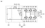
- FIG. 2 is a circuit diagram of the circuit device 100;
- FIG. 2 is an exploded perspective view of the circuit device 100;
- FIG. 4 is a plan view of a first partition plate 41;
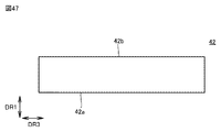
- FIG. 4 is a plan view of a second partition plate 42;
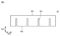
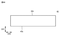
- FIG. 4 is a plan view of a third partition plate 43;
- FIG. 3 is a cross-sectional view taken along line VI-VI in FIG. 2;
- FIG. 3A to 3C are process diagrams showing a method of assembling the circuit device 100;
- 3 is a cross-sectional view of the circuit device 100A;
- FIG. 2 is a cross-sectional view of the circuit device 100B;
- FIG. FIG. 4 is a cross-sectional view of the circuit device 100C;
- FIG. 4 is a top view of a third partition plate 43 included in the circuit device 100D; 2 is a cross-sectional view of the circuit device 200; FIG. 4 is a perspective view of a first partition plate 41 included in the circuit device 200; FIG. 4 is a perspective view of a second partition plate 42 included in the circuit device 200.
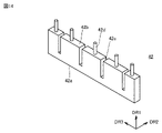
- FIG. 3 is a perspective view of a third partition plate 43 included in the circuit device 200;
- FIG. 4A to 4C are process diagrams showing a method of assembling the circuit device 200; 2 is a cross-sectional view of the circuit device 200A;
- FIG. 4 is a plan view of a first partition plate 41 included in the circuit device 200A;
- FIG. FIG. 4 is a plan view of a second partition plate 42 included in the circuit device 200A;
- FIG. 4 is a plan view of a third partition plate 43 included in the circuit device 200A; 2 is a cross-sectional view of the circuit device 200B; FIG. 2 is a circuit diagram of a circuit device 200B; FIG. 3 is a cross-sectional view of the circuit device 300; FIG. 4 is a perspective view of a first partition plate 41 included in the circuit device 300. FIG. 4 is a perspective view of a second partition plate 42 included in the circuit device 300. FIG. 4 is a perspective view of a third partition plate 43 included in the circuit device 300; FIG. 3A to 3C are process diagrams showing a method of assembling the circuit device 300; 4 is an exploded perspective view of the circuit device 400; FIG. FIG.
- FIG. 29 is a cross-sectional view along XXIX-XXIX in FIG. 28; 4 is a perspective view of a third partition plate 43 included in the circuit device 400; FIG. 4 is a cross-sectional view of the circuit device 400A; FIG. 4 is a perspective view of a third partition plate 43 included in the circuit device 400A; FIG. 3 is an exploded perspective view of the circuit device 500; FIG. FIG. 34 is a cross-sectional view taken along line XXXIV-XXXIV in FIG. 33; 4 is a perspective view of a first partition plate 41 included in the circuit device 500; FIG. 4 is a perspective view of a second partition plate 42 included in the circuit device 500.
- FIG. 3 is a perspective view of a third partition plate 43 included in the circuit device 500;
- FIG. 6 is an exploded perspective view of the circuit device 600;
- FIG. FIG. 39 is a cross-sectional view along XXXIX-XXXIX in FIG. 38;
- 4 is a perspective view of a third partition plate 43 included in the circuit device 600;
- FIG. 7 is an exploded perspective view of the circuit device 700;
- FIG. 4 is a plan view of a first partition plate 41 included in the circuit device 700;
- FIG. 4 is a plan view of a second partition plate 42 included in the circuit device 700.
- FIG. 3 is a plan view of a third partition plate 43 included in the circuit device 700;
- FIG. 7 is an exploded perspective view of the circuit device 700A;
- FIG. 4 is a plan view of a first partition plate 41 included in the circuit device 700A; 7 is a plan view of a second partition plate 42 included in the circuit device 700A; FIG. FIG. 4 is a plan view of a third partition plate 43 included in the circuit device 700A; 7 is an exploded perspective view of the circuit device 700B; FIG.
- circuit device 100 A circuit device (hereinafter referred to as “circuit device 100”) according to Embodiment 1 will be described.
- the circuit device 100 is, for example, a power conversion device. Although the circuit device 100 is not limited to a power conversion device, the power conversion device will be described below as an example of the circuit device 100 .
- FIG. 1 is a circuit diagram of a circuit device 100. As shown in FIG. As shown in FIG. 1, the circuit device 100 has a peripheral circuit 110 and a switching circuit 120 .
- the peripheral circuit 110 has a plurality of circuit components 10.
- the plurality of circuit components 10 are a capacitor 10a, an inductor 10b, a contactor 10c, a discharging resistor 10d and a charging resistor 10e.
- Capacitor 10a, inductor 10b and contactor 10c are connected in series.
- Inductor 10b is arranged between capacitor 10a and contactor 10c.
- a discharging resistor 10d and a charging resistor 10e are connected in parallel to the capacitor 10a and the contactor 10c, respectively.
- Peripheral circuit 110 is connected to DC supply circuit 130 .
- the switching circuit 120 is, for example, a three-phase inverter circuit.
- the switching circuit 120 has multiple circuit components 20 .
- the plurality of circuit components 20 are transistors 20a-20f and diodes 20g-20l.
- the drain of the transistor 20a is electrically connected to one electrode of the capacitor 10a.
- the source of transistor 20a is electrically connected to the drain of transistor 20b.
- the source of transistor 20b is electrically connected to the other electrode of capacitor 10a.
- the anode of diode 20g is electrically connected to the source of transistor 20a.
- the cathode of diode 20g is electrically connected to the drain of transistor 20a.
- the anode of diode 20h is electrically connected to the source of transistor 20b.
- the cathode of diode 20h is electrically connected to the drain of transistor 20b.
- the transistor 20c, the transistor 20d, the diode 20i and the diode 20j are connected in the same manner as the transistor 20a, the transistor 20b, the diode 20g and the diode 20h, respectively.
- Transistor 20e, transistor 20f, diode 20k, and diode 20l are connected in the same manner as transistor 20a, transistor 20b, diode 20g, and diode 20h, respectively.
- the gates of transistors 20a-20f are connected to a control circuit.
- the switching circuit 120 is connected to the motor 140.
- Motor 140 is, for example, a three-phase motor.
- Motor 140 has input line 141 , input line 142 , and input line 143 .
- the input line 141 is electrically connected to the source of the transistor 20a and the drain of the transistor 20b.
- the input line 142 is electrically connected to the source of the transistor 20c and the drain of the transistor 20d.
- the input line 143 is electrically connected to the source of the transistor 20e and the drain of the transistor 20f.
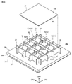
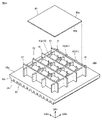
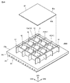
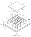
- FIG. 2 is an exploded perspective view of the circuit device 100.
- the circuit device 100 has a heat sink 30, a plurality of first partition plates 41, and a plurality of second partition plates .
- the heat sink 30 has an upper surface 30a and a lower surface 30b.
- the upper surface 30a is orthogonal to the first direction DR1.
- the lower surface 30b is the opposite surface of the upper surface 30a.
- a direction perpendicular to the first direction DR1 is defined as a second direction DR2.
- a direction perpendicular to the first direction DR1 and the second direction DR2 is defined as a third direction DR3.
- a plurality of fins 30c are formed on the lower surface 30b.
- the fin 30c extends, for example, in the second direction DR2.
- the plurality of fins 30c are spaced apart from each other in the third direction DR3.
- the heat sink 30 is made of a metal material having excellent thermal conductivity, such as copper (copper alloy) or aluminum (aluminum alloy).
- the heat sink 30 is formed by extrusion, for example. Extrusion is performed, for example, along the extending direction (second direction DR2) of the fins 30c.
- the first partition plate 41 is attached to the upper surface 30a.
- the first partition plate 41 extends in the second direction DR2.
- the plurality of first partition plates 41 are spaced apart from each other in the third direction DR3.
- a rolled material made of a metal material having excellent thermal conductivity such as copper (copper alloy) or aluminum (aluminum alloy) is used.
- the second partition plate 42 is attached to the upper surface 30a.
- the second partition plate 42 extends in the third direction DR3.
- the plurality of second partition plates 42 are spaced apart from each other in the second direction DR2.
- the first partition plate 41 and the second partition plate 42 are attached to the upper surface 30a in a grid pattern.
- a rolled material made of a metal material having excellent thermal conductivity such as copper (copper alloy) or aluminum (aluminum alloy) is used.
- a third partition plate 43 is the first partition plate 41 that is arranged other than both ends in the third direction DR3.
- the number of third partition plates 43 is at least one. In the example shown in FIG. 2, the number of third partition plates 43 is two.
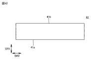
- FIG. 3 is a plan view of the first partition plate 41.
- the first partition plate 41 has a first end 41a and a second end 41b.
- the first end 41a is the end on the upper surface 30a side.
- the second end 41b is the end opposite to the first end 41a.
- a plurality of first insertion openings 41c are formed in the first partition plate 41 at intervals in the second direction DR2.
- the first insertion port 41c extends from the first end 41a toward the second end 41b.
- the first insertion port 41c penetrates the first partition plate 41 along the thickness direction.
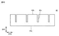
- FIG. 4 is a plan view of the second partition plate 42.
- the second partition plate 42 has a third end 42a and a fourth end 42b.
- the third end 42a is the end on the upper surface 30a side.
- the fourth end 42b is the end opposite to the third end 42a.
- a plurality of second insertion openings 42c are formed in the second partition plate 42 at intervals in the third direction DR3.
- the second insertion port 42c extends from the fourth end 42b toward the third end 42a.
- the second insertion port 42c penetrates the second partition plate 42 along the thickness direction.
- FIG. 5 is a plan view of the third partition plate 43.
- the third partition plate 43 has a fifth end 43a and a sixth end 43b.
- the fifth end 43a is the end on the upper surface 30a side.
- the sixth end 43b is the end opposite to the fifth end 43a.
- a plurality of third insertion openings 43c are formed in the third partition plate 43 at intervals in the second direction DR2.
- the third insertion port 43c extends from the fifth end 43a toward the sixth end 43b.
- the third insertion port 43c penetrates the third partition plate 43 along the thickness direction.
- a second insertion port 42c is inserted into the first insertion port 41c and the third insertion port 43c. This prevents the first partition plate 41, the third partition plate 43, and the second partition plate 42 from interfering with each other.
- the thickness of the third partition plate 43 in the third direction DR3 is preferably greater than the thickness of the first partition plate 41 in the third direction DR3. From another point of view, the contact area between the third partition plate 43 and the top surface 30a is preferably larger than the contact area between the first partition plate 41 and the top surface 30a.
- the first partition plate 41, the second partition plate 42 and the third partition plate 43 can be manufactured by any method.
- the first partition plate 41, the second partition plate 42, and the third partition plate 43 may be manufactured, for example, by punching a plate-like member, or milling the plate-like member. may be manufactured by Also, the first partition plate 41, the second partition plate 42 and the third partition plate 43 may be manufactured by extrusion molding.
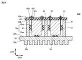
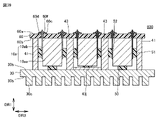
- FIG. 6 is a cross-sectional view taken along line VI-VI in FIG.
- the capacitor 10a (circuit component 10) includes two adjacent first partition plates 41 (adjacent first partition plate 41 and third partition plate 43 or two adjacent third partition plates 43). ) and the two adjacent second partition plates 42 and the upper surface 30a.
- the circuit component 10 has a circuit component body and lead wires.
- the circuit component main body is the capacitor element main body 10aa and the lead wire is the lead wire 10ab.
- the lead wire 10ab is electrically connected to the capacitor element body 10aa.
- Circuit device 100 further includes adhesive 50 , heat transfer member 51 , heat transfer member 52 , and substrate 60 .
- the adhesive 50 is placed between the top surface of the capacitor 10a and the top surface 30a.
- the adhesive 50 is made of, for example, a resin material such as silicone resin, epoxy resin, or urethane resin.
- a thermally conductive filler may be mixed in the adhesive 50 in order to improve thermal conductivity.
- the thermally conductive filler is made of, for example, metal material or ceramic material.
- the adhesive 50 may be made of a material having a thermal conductivity of, for example, 1 W/m ⁇ K or more and several tens of W/m ⁇ K or less.
- a heat transfer member 51 is arranged between the capacitor 10 a and the first partition plate 41 . More specifically, the heat transfer member 51 is arranged between the first partition plate 41 and the surface of the capacitor element main body 10aa to which the lead wires 10ab are attached, or between the first partition plate 41 and the lead wires 10ab. It is The heat transfer member 51 may be arranged both between the first partition plate 41 and the surface of the capacitor element main body 10aa to which the lead wires 10ab are attached and between the first partition plate 41 and the lead wires 10ab. good.
- a heat transfer member 52 is arranged between the capacitor 10 a and the third partition plate 43 . More specifically, the heat transfer member 52 is arranged between the third partition plate 43 and the surface of the capacitor element body 10aa to which the lead wires 10ab are attached, or between the third partition plate 43 and the lead wires 10ab. It is The heat transfer member 52 may be arranged both between the third partition plate 43 and the surface of the capacitor element main body 10aa to which the lead wires 10ab are attached and between the third partition plate 43 and the lead wires 10ab. good.
- the heat transfer member 51 and the heat transfer member 52 are made of a resin material such as silicone resin, epoxy resin, or urethane resin.
- a thermally conductive filler may be mixed in the heat transfer member 51 and the heat transfer member 52 in order to improve the thermal conductivity.
- the thermally conductive filler is made of, for example, metal material or ceramic material.
- the heat transfer member 51 and the heat transfer member 52 may be made of a material having a thermal conductivity of, for example, 1 W/m ⁇ K or more and several tens of W/m ⁇ K or less.
- the substrate 60 has a first main surface 60a and a second main surface 60b.
- the second main surface 60b is the so-called mounting surface (C surface) of the substrate 60.
- the second principal surface 60b is the opposite surface of the first principal surface 60a.
- the second major surface 60b is in contact with the second end 41b, the fourth end 42b and the sixth end 43b.
- the base material of the substrate 60 is, for example, a ceramic substrate such as a paper phenol substrate, a paper epoxy substrate, a glass composite substrate, a glass epoxy substrate, a polyimide substrate, an alumina substrate, or an aluminum core substrate.
- the substrate 60 may be a so-called flexible substrate.
- An insulating layer made of an insulating material may be arranged between the first main surface 60a and the second main surface 60b. Resin materials such as urethane resins, silicone resins, and epoxy resins having a thermal conductivity of 1 W/m ⁇ K to several tens of W/m ⁇ K can be used as the insulating material. An insulating layer may be disposed between the conductive layers of substrate 60 .
- a circuit pattern 60c is formed on the first main surface 60a.
- the thickness of the circuit pattern 60c is, for example, 1 ⁇ m or more and 200 ⁇ m or less.
- the circuit pattern 60c is made of a conductive material. Conductive materials are copper, nickel, aluminum, silver, tin or alloys thereof.
- the circuit pattern 60c may be formed inside the second main surface 60b and the substrate 60 as well.
- a through-hole 60d is formed in the substrate 60, penetrating the substrate 60 along the thickness direction.
- the through hole 60d is, for example, circular in plan view.
- the inner diameter of the through hole 60d is, for example, 0.6 mm or more and 1.5 mm or less.
- a conductor film 60e (not shown) is formed on the inner wall surface of the through hole 60d.
- the thickness of the conductor film 60e is, for example, 0.01 mm or more and 0.1 mm or less.
- the conductor film 60e is electrically connected to the circuit pattern 60c.
- a capacitor 10 a is connected to the substrate 60 . More specifically, while the lead wire 10ab is inserted into the through hole 60d, the lead wire 10ab is connected to the conductor film 60e and the circuit pattern 60c around the through hole 60d by the connecting member 60f.
- the connection member 60f is made of, for example, a solder alloy.
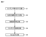
- FIG. 7 is a process diagram showing a method of assembling the circuit device 100.
- the method of assembling the circuit device 100 includes a capacitor attachment step S1, a partition plate attachment step S2, an adhesive application step S3, and a capacitor accommodation step S4.
- the capacitor 10a is attached to the substrate 60. More specifically, while the lead wire 10ab is inserted into the through hole 60d, the lead wire 10ab is soldered to the conductor film 60e and the circuit pattern 60c around the through hole 60d. This soldering is performed, for example, by flow soldering.
- the first partition plate 41 (the third partition plate 43) and the second partition plate 42 are attached to the heat sink 30.
- the first partition plate 41 (the third partition plate 43) and the second partition plate 42 are attached to the heat sink 30 by, for example, an adhesive applied to the upper surface 30a.
- the method of attaching the first partition plate 41 (the third partition plate 43) and the second partition plate 42 to the heat sink 30 is not limited to this.
- the first partition plate 41 (the third partition plate 43) and the second partition plate 42 are attached to the heat sink 30 by attaching the first partition plate 41 (the third partition plate 43) and the second partition plate 41 (the third partition plate 43) to the caulking grooves formed in the upper surface 30a. It may be done by crimping the plate 42 .
- the first partition plate 41 (third partition plate 43) and the second partition plate 42 are attached to the upper surface 30a (heat sink 30) by brazing while being inserted into grooves formed in the upper surface 30a. may be
- the adhesive 50 is applied onto the upper surface 30a.
- the heat transfer member 51 and the heat transfer member 52 may be applied to the lead wire 10ab (side surface of the capacitor 10a).
- the capacitor housing step S4 the capacitor 10a is placed between two adjacent first partition plates 41 (adjacent first partition plate 41 and third partition plate 43 or two adjacent third partition plates 43) and two adjacent first partition plates 41 and 43, respectively. It is housed in the space surrounded by the partition plate 42 and the upper surface 30a. As a result, the top surface of the capacitor 10a contacts the upper surface 30a through the adhesive 50, and the side surfaces of the capacitor 10a contact the first partition plate 41 (the third partition plate 43) through the heat transfer member 51 (heat transfer member 52). ).
- first heat radiation path heat generated in the capacitor 10a (capacitor element body 10aa) is radiated from the heat sink 30 via the top surface of the capacitor 10a and the adhesive 50 (hereinafter referred to as "first heat radiation path"). Therefore, according to the circuit device 100, the temperature rise of the capacitor 10a due to the operation of the circuit device 100 can be suppressed.
- the first heat dissipation path consists of the capacitor 10a between the first partition plate 41 and the third partition plate 43 (capacitor 10a at the end) and the capacitor 10a between two adjacent third partition plates 43 (capacitor 10a in the middle). It works the same for both capacitors 10a). Therefore, according to the circuit device 100a, the temperature gradient between the capacitors 10a at the ends and the capacitor 10a at the center can be reduced.
- the heat generated in the capacitor 10a passes through the side surface (lead wire 10ab) of the capacitor 10a, the heat transfer member 51 (heat transfer member 52), and the first partition plate 41 (third partition plate 43). , heat is radiated from the heat sink (hereinafter referred to as “second heat radiation path”). Therefore, according to the circuit device 100, heat can be dissipated through the second heat dissipation path in addition to the first heat dissipation path, and the temperature rise of the capacitor 10a due to the operation of the circuit device 100 can be further suppressed.
- the contact area between the third partition plate 43 and the upper surface 30a is larger than the contact area between the first partition plate 41 and the upper surface 30a. Therefore, the contact thermal resistance value between the third partition plate 43 and the upper surface 30a is smaller than the contact thermal resistance value between the first partition plate 41 and the upper surface 30a.
- the capacitors 10a are arranged on both sides of the third partition plate 43 .
- the capacitor 10a is arranged only on one side of the first partition plate 41 . Therefore, the third partition plate 43 receives a larger amount of heat from the capacitor 10a than the first partition plate 41 does.
- ⁇ t is the temperature rise value of the partition plate
- Q is the amount of heat from the capacitor 10a
- Ra is the thermal resistance value of the partition plate
- Rb is the contact thermal resistance value of the partition plate.
- the third partition plate 43 has a contact area with the upper surface 30a and a thickness larger than those of the first partition plate 41 . From another point of view, Ra and Rb of the third partition plate 43 are smaller than Ra and Rb of the first partition plate 41 . Therefore, according to the circuit device 100, even if the value of Q is large in the third partition plate 43, an increase in ⁇ t can be suppressed, and the capacitor 10a between the first partition plate 41 and the third partition plate 43 adjacent to each other can be suppressed. and the capacitor 10a between the two adjacent third partition plates 43 can be further reduced.
- the substrate 60 is used for connecting the capacitor 10a.
- the insulating base material of the substrate 60 is between the lead wire 10ab on the positive electrode side and the lead wire 10ab on the negative electrode side. Contact between the lead wire 10ab and the lead wire 10ab on the negative electrode side is prevented.
- vibration resistance and impact resistance can be improved.
- the circuit board 60 enables complicated and high-density wiring, so high-density mounting of the capacitors 10a becomes possible.
- the first partition plate 41 the second partition plate 42 and the third partition plate 43
- the thermal constraint can be reduced.
- An electrically optimum arrangement of the capacitor 10a is possible without receiving the voltage.
- the first partition plate 41, the second partition plate 42, and the third partition plate 43 function as electromagnetic shields.
- the circuit component 10 is the inductor 10b
- leakage magnetic flux from the inductor 10b is shielded by the first partition plate 41, the second partition plate 42, and the third partition plate 43, so that magnetic interference with other inductors 10b occurs. is suppressed.
- the first partition plate 41, the second partition plate 42, and the third partition plate 43 function as firewalls. For example, when a discharge spark is generated from the capacitor 10a due to a failure of the capacitor 10a, the spark is blocked by the first partition plate 41, the second partition plate 42, and the third partition plate 43, and the impact on the other capacitors 10a is prevented. prevented.
- the two adjacent first partitions 41 are arranged according to the number and size of the capacitors 10a. Number and size of spaces surrounded by (adjacent first partition plate 41 and third partition plate 43 or two adjacent third partition plates 43), two adjacent second partition plates 42, and upper surface 30a can be changed.
- the thickness, type, thickness, etc. of the first partition plate 41, the second partition plate 42, and the third partition plate 43 can be arbitrarily selected.
- various uses can be realized flexibly at low cost.
- the thermal conductivity of the lead wire 10ab is higher than that of the capacitor element body 10aa, and the heat generated in the capacitor element body 10aa is easily conducted to the lead wire 10ab. Therefore, when the heat transfer member 51 (heat transfer member 52) is arranged between the first partition plate 41 (third partition plate 43) and the lead wire 10ab, the heat dissipation from the second heat dissipation path is maintained while the heat transfer The usage amount of the heat member 51 (heat transfer member 52) can be suppressed. That is, in this case, the weight of the circuit device 100 can be reduced.
- the heat transfer member 51 heat transfer member 52
- the first partition plate 41 third partition plate 43
- the thickness of the heat transfer member 51 heat transfer member 52
- heat dissipation from the second heat dissipation path can be improved based on Equation 2 described later.
- the conductive heat transfer member 51 since the insulation between the lead wire 10ab and the first partition plate 41 (the third partition plate 43) can be ensured, the conductive heat transfer member 51 (heat transfer member 52) is used. be able to.
- the conductive heat transfer member 51 (heat transfer member 52) has higher thermal conductivity than the insulating heat transfer member 51 (heat transfer member 52). Therefore, in this case, the heat dissipation from the second heat dissipation path can be further enhanced.
- the heat transfer member 51 (heat transfer member 52) is positioned between the first partition plate 41 (third partition plate 43) and the lead wire 10ab and between the heat transfer member 51 (heat transfer member 52) and the first partition plate 41 ( When the third partition plate 43) and the surface of the capacitor element body 10aa to which the lead wires 10ab are attached, the area of the heat transfer member 51 (heat transfer member 52) is increased. Based on Equation 2, heat dissipation from the second heat dissipation path is improved. As the contact area between the heat transfer member 51 (heat transfer member 52) and the first partition plate 41 (third partition plate 43) increases, the heat transfer member 51 (heat transfer member 52) is less likely to separate.
- the heat transfer member 51 heat transfer member 52
- the heat transfer member 51 heat transfer member 52
- the heat transfer member 51 heat transfer member 52
- the heat transfer member 51 heat transfer member 52
- the heat transfer member 51 is arranged between the first partition plate 41 (third partition plate 43) and the surface of the capacitor element body 10aa to which the lead wires 10ab are attached
- the heat transfer It is necessary to apply the heat member 51 (heat transfer member 52) so as not to adhere to the lead wire 10ab.
- heat transfer member 51 heat transfer member 52
- the heat transfer member 51 is positioned between the first partition plate 41 (third partition plate 43) and the lead wire 10ab and the heat transfer member 51 (heat transfer member 52) is positioned between the first partition plate 41 (third partition plate 43) and the lead wire 10ab. If the partition plate 43) and the surface of the capacitor element main body 10aa to which the lead wires 10ab are attached, the heat transfer member 51 (heat transfer member 52) can be simplified.
- circuit device 100A A circuit device 100 (hereinafter referred to as “circuit device 100A”) according to Modification 1 will be described.
- FIG. 8 is a cross-sectional view of the circuit device 100A.
- FIG. 8 shows a cross section of the circuit device 100A at a position corresponding to VI-VI in FIG.
- the capacitor 10a further includes an exterior case 10ac and a sealing resin 10ad.
- a capacitor element main body 10aa and lead wires 10ab are arranged in an exterior case 10ac.
- the sealing resin 10ad seals the capacitor element main body 10aa and the lead wires 10ab by filling the exterior case 10ac.
- the circuit device 100 it is necessary to increase the thickness of the heat transfer member 51 (heat transfer member 52) in order to secure the insulation distance between the lead wire 10ab and the first partition plate 41 (third partition plate 43). be.
- the insulation between the lead wires 10ab and the first partition plate 41 (the third partition plate 43) can be ensured by the exterior case 10ac. ) can be reduced.
- R is the thermal resistance of the heat transfer member 51 (heat transfer member 52)
- L is the thickness of the heat transfer member 51 (heat transfer member 52)
- ⁇ is the heat transfer member 51 (heat transfer member 52 )
- a c is the cross-sectional area of the heat transfer member 51 (heat transfer member 52).
- circuit device 100B A circuit device 100 (hereinafter referred to as “circuit device 100B”) according to Modification 2 will be described.
- FIG. 9 is a cross-sectional view of the circuit device 100B.
- FIG. 9 shows a cross-sectional view of the circuit device 100B at a position corresponding to VI-VI in FIG.
- the substrate 60 is not formed with the through holes 60d.
- the circuit pattern 60c connected to the lead wire 10ab is arranged on the second main surface 60b.
- the method of assembling the circuit device 100B differs from the method of assembling the circuit device 100 with respect to the capacitor mounting step S1.
- the connection member 60f is applied onto the circuit pattern 60c on the second main surface 60b using, for example, a printing machine.
- the capacitor 10a is arranged such that the lead wire 10ab is positioned on the connecting member 60f.
- reflow soldering is performed by heating the connection member 60f to a temperature higher than its melting point, and the lead wire 10ab and the circuit pattern 60c are joined by the connection member 60f.
- circuit device 100C A circuit device 100 (hereinafter referred to as “circuit device 100C”) according to Modification 3 will be described.
- FIG. 10 is a cross-sectional view of the circuit device 100C.
- FIG. 10 shows a cross section of the circuit device 100C at a position corresponding to VI-VI in FIG.
- a sealing member 53 is used as the heat transfer member 51 and the heat transfer member 52 .
- the sealing member 53 includes two adjacent first partition plates 41 (adjacent first partition plate 41 and third partition plate 43 or two adjacent third partition plates 43) and two adjacent second partition plates 42. and the upper surface 30a.
- the capacitor 10a has two adjacent first partition plates 41 (adjacent first partition plate 41 and third partition plate 43 or two adjacent third partition plates 43) and two adjacent second partition plates. 42, the third partition plate 43 and the upper surface 30a are sealed by a sealing member 53. As shown in FIG.
- the sealing member 53 is made of an electrically insulating material.
- the thermal conductivity of the material forming the sealing member 53 is preferably 0.1 W/m ⁇ K or more. More preferably, the thermal conductivity of the material forming the sealing member 53 is 1.0 W/m ⁇ K or more.
- the Young's modulus of the material forming the sealing member 53 is preferably 1 MPa or more.
- the sealing member 53 is made of a resin material such as polyphenylene sulfide (PPS), polyetheretherketone (PEEK), or the like, which contains a thermally conductive filler.
- the sealing member 53 may be made of a rubber material such as epoxy, silicone, or urethane.
- heat from the capacitor 10a is radiated from the heat sink 30 through the side surface of the capacitor 10a, the sealing member 53, and the first partition plate 41 (third partition plate 43) in addition to the first heat dissipation path. (hereinafter referred to as “third heat dissipation path”).
- heat can be radiated through the first heat dissipation path and the third heat dissipation path, so that the temperature rise of the capacitor 10a due to the operation of the circuit device 100B can be suppressed.
- circuit device 100D A circuit device 100 (hereinafter referred to as “circuit device 100D”) according to Modification 4 will be described.
- FIG. 11 is a top view of the third partition plate 43 of the circuit device 100D.
- the third partition plate 43 extends in the second direction DR2 in a zigzag shape in the second direction DR2 when viewed from the first direction DR1.
- the thickness of the third partition plate 43 in the third direction DR3 may be greater than the thickness of the first partition plate 41 in the third direction DR3. may be equal to the thickness.
- the third partition plate 43 extends in a zigzag shape when viewed from the first direction DR1.
- the contact thermal resistance between 43 and top surface 30a is reduced. Therefore, according to the circuit device 100D, the temperature gradient between the capacitor 10a between the adjacent first partition plate 41 and the third partition plate 43 and the capacitor 10a between the two adjacent third partition plates 43 is can be further reduced.
- any of the capacitor 10a, the inductor 10b, the contactor 10c, the discharge resistor 10d, and the charge resistor 10e may be arranged as the circuit component 10 used in the circuit devices 100 to 100D. Any component that generates heat can be used as the circuit component 10 in the circuit device 100 to the circuit device 100D.
- only one circuit component 10 may be arranged in one section, or a plurality of circuit components 10 may be arranged in one section.
- the one circuit component 10 can use all the cooling capacity of the one section.
- the cooling capacity is divided, but if the circuit components 10 are small and the compartment is large, the circuit components 10 can be arranged more efficiently.
- the circuit device 100 to the circuit device 100D may have a section (arrangement section) where the circuit component 10 is arranged and a section (non-arrangement section) where the circuit component 10 is not arranged.
- the cooling effect of the circuit components 10 arranged in the arrangement section adjacent to the non-arrangement section can be further enhanced, and the circuit components 10 can be cooled more effectively.
- circuit device 200 A circuit device (hereinafter referred to as "circuit device 200") according to the second embodiment will be described. Differences from circuit device 100 will be mainly described below, and redundant description will not be repeated.
- FIG. 12 is a cross-sectional view of the circuit device 200.
- FIG. FIG. 12 shows a cross section of the circuit device 200 at a position corresponding to VI-VI in FIG.
- FIG. 13 is a perspective view of the first partition plate 41 included in the circuit device 200.
- FIG. 14 is a perspective view of the second partition plate 42 included in the circuit device 200.
- FIG. FIG. 15 is a perspective view of the third partition plate 43 included in the circuit device 200.
- the circuit device 200 includes a circuit component 10 (capacitor 10a), a heat sink 30, a plurality of first partition plates 41, a plurality of second partition plates 42, and an adhesive 50. , a heat transfer member 51 , a heat transfer member 52 , and a substrate 60 .
- the first partition plates 41 located other than the two ends in the third direction DR3 are the third partition plates 43 .
- the configuration of the circuit device 200 is common to the configuration of the circuit device 100.
- the first partition plate 41, the second partition plate 42 and the third partition plate 43 have terminals 41d, 42d and 43d, respectively.
- the configuration of circuit device 200 differs from that of circuit device 100 .
- the terminal 41d protrudes from the second end 41b along the first direction DR1.
- the terminal 41d is integrally formed of the same material as the first partition plate 41, for example.
- the terminal 42d protrudes from the fourth end 42b along the first direction DR1.
- 42 d of terminals are integrally formed with the material same as the 2nd partition plate 42, for example.
- the terminal 43d protrudes from the sixth end 43b along the first direction DR1.
- 43 d of terminals are integrally formed with the same material as the 3rd partition plate 43, for example.
- the terminal 41d, the terminal 42d, and the terminal 43d are formed, for example, by cutting the first partition plate 41, the second partition plate 42, and the third partition plate 43, respectively.
- the terminals 41d, 42d and 43d are inserted into the through holes 60d.
- the through holes 60d into which the terminals 41d, 42d and 43d are inserted are different from the through holes 60d into which the lead wires 10ab are inserted.
- Plating is preferably formed on the surfaces of the terminals 41d, 42d, and 43d. This plating is made of, for example, a metal material that is easy to solder. This plating is made of, for example, copper, tin, nickel, brass, or the like.
- the terminals 41d, 42d and 43d are preferably soldered to the circuit pattern 60c around the through hole 60d.
- FIG. 16 is a process diagram showing a method of assembling the circuit device 200.
- the method of assembling the circuit device 200 includes a capacitor attachment step S1, a partition plate attachment step S2, and an adhesive application step S3.
- the method of assembling circuit device 200 is common to the method of assembling circuit device 100 .
- the method for assembling the circuit device 200 does not have the capacitor housing step S4. Further, in the capacitor mounting step S1 in the method of assembling the circuit device 200, flow soldering of the terminals 41d, 42d and 43d is performed in addition to the flow soldering of the lead wires 10ab. Furthermore, in the method for assembling the circuit device 200, the partition plate attachment step S2 is performed after the adhesive application step S3. In this regard, the method of assembling circuit device 200 is different from the method of assembling circuit device 100 .
- the substrate 60 has a high temperature due to the heat from the capacitor 10a.
- the heat of the substrate 60 is sequentially transferred to the capacitor 10a, the heat transfer member 51 (heat transfer member 52), the first partition plate 41 (third partition plate 43), and the heat sink 30. Heat is dissipated.
- the heat of the substrate 60 is sequentially transferred to the terminal 41d (terminal 43d), the first partition plate 41 (third partition plate 43), and the heat sink, and radiated from the heat sink 30 (hereinafter referred to as referred to as a “fourth heat dissipation path”). That is, in circuit device 200 , the heat dissipation path for heat from substrate 60 is shortened compared to circuit device 100 . Thus, the circuit device 200 can suppress the temperature rise of the substrate 60 by having the fourth heat dissipation path, so that the temperature rise of the capacitor 10a connected to the substrate 60 can be further suppressed. can be done.
- circuit device 200A A circuit device 200 (hereinafter referred to as “circuit device 200A”) according to Modification 1 will be described.
- FIG. 17 is a cross-sectional view of the circuit device 200A.
- FIG. 17 shows a cross section of the circuit device 200A at a position corresponding to VI-VI in FIG.
- FIG. 18 is a plan view of the first partition plate 41 included in the circuit device 200A.
- FIG. 19 is a plan view of the second partition plate 42 included in the circuit device 200A.
- FIG. 20 is a plan view of the third partition plate 43 included in the circuit device 200A.
- an upright wall portion 41ea and an upright wall portion 41eb are formed on the side surface of the first partition plate 41.
- the standing wall portion 41ea and the standing wall portion 41eb face each other with a gap in the second direction DR2.
- the terminal 41d is arranged between the vertical wall portion 41ea and the vertical wall portion 41eb.
- the terminal 41d is attached to the first partition plate 41 by crimping the upright wall portion 41ea and the upright wall portion 41eb.
- the side surface of the second partition plate 42 is formed with an upright wall portion 42ea and an upright wall portion 42eb.
- the standing wall portion 42ea and the standing wall portion 42eb face each other with a gap in the third direction DR3.
- the terminal 42d is arranged between the vertical wall portion 42ea and the vertical wall portion 42eb.
- the terminal 42d is attached to the second partition plate 42 by crimping the upright wall portion 42ea and the upright wall portion 42eb.
- the side surface of the third partition plate 43 is formed with an upright wall portion 43ea and an upright wall portion 43eb.
- the standing wall portion 43ea and the standing wall portion 43eb face each other with a gap in the second direction DR2.
- the terminal 43d is arranged between the vertical wall portion 43ea and the vertical wall portion 43eb.
- the terminal 43d is attached to the third partition plate 43 by crimping the upright wall portion 43ea and the upright wall portion 43eb.
- the terminals 41d, 42d, and 43d are preferably made of a metal material that is easy to solder, such as copper, tin, nickel, and brass.
- the surfaces of the terminals 41d, 42d, and 43d may not be plated.
- the first partition plate 41 having the standing wall portions 41ea and 41eb, the second partition plate 42 having the standing wall portions 42ea and 42eb, and the third partition plate 43 having the standing wall portions 43ea and 43eb are formed by milling. It may be formed by extrusion molding. However, the processing method for the first partition plate 41, the second partition plate 42, and the third partition plate 43 is not limited to the above.
- the first partition plate 41, the second partition plate 42, and the third partition plate 43 are formed of a material such as aluminum that is difficult to solder, the surfaces of the terminals 41d, 42d, and 43d may have Plating must be done with a material that is easy to solder.
- the terminals 41d, 42d and 43d can be made of a material different from that of the first partition 41, second partition 42 and third partition 43. Therefore, according to the circuit device 200A, even if the first partition plate 41, the second partition plate 42, and the third partition plate 43 are made of a material that is difficult to solder, the terminals 41d, 42d, and 43d can be soldered. If they are made of a material that is easy to attach, it is possible to omit the process of plating the surfaces of the terminals 41d, 42d, and 43d.
- circuit device 200B A circuit device 200 (hereinafter referred to as “circuit device 200B”) according to modification 2 will be described.
- FIG. 21 is a cross-sectional view of the circuit device 200B.
- FIG. 21 shows a cross section of the circuit device 200B at a position corresponding to VI-VI in FIG.
- FIG. 22 is a circuit diagram of the circuit device 200B.
- the lead wire 10ab forming the negative electrode of the capacitor 10a is referred to as a lead wire 10ae.
- the terminals 41d, 42d and 43d are connected to a circuit pattern 60c which is connected to the lead wire 10ae.
- the negative electrode of the DC supply circuit 130 is connected to the ground terminal.
- the substrate 60 becomes hot at the connection with the lead wire 10ae.
- the connection portion of the lead wire 10ae is connected to the terminals 41d, 42d and 43d by the circuit pattern 60c. Since the thermal conductivity of the circuit pattern 60c is higher than the thermal conductivity of the base material of the substrate 60, in the circuit device 200B, the thermal resistance of the substrate 60 in the fourth heat dissipation path is reduced, and the heat dissipation from the fourth heat dissipation path is improved. further enhanced.
- the heat sink 30 (including the first partition plate 41 , the second partition plate 42 and the third partition plate 43 ) is grounded, the heat sink 30 can function as the negative electrode wiring of the DC supply circuit 130 . Therefore, in this case, the wires required for the DC supply circuit 130 and the circuit pattern 60c formed on the substrate 60 can be reduced.
- circuit device 300 A circuit device (hereinafter referred to as "circuit device 300") according to the third embodiment will be described. Differences from circuit device 100 will be mainly described below, and redundant description will not be repeated.
- circuit device 300 (Configuration of circuit device 300) The configuration of the circuit device 300 will be described below.
- FIG. 23 is a cross-sectional view of the circuit device 300.
- FIG. FIG. 23 shows a cross section of the circuit device 300 at a position corresponding to VI-VI in FIG.
- FIG. 24 is a perspective view of the first partition plate 41 included in the circuit device 300.
- FIG. FIG. 25 is a perspective view of the second partition plate 42 included in the circuit device 300.
- FIG. 26 is a perspective view of the third partition plate 43 included in the circuit device 300.
- the circuit device 300 as shown in FIGS. , a heat transfer member 51 , a heat transfer member 52 , and a substrate 60 .
- the first partition plates 41 located other than the two ends in the third direction DR3 are the third partition plates 43 .
- the configuration of circuit device 300 is common to the configuration of circuit device 100 .
- a screw hole 41f, a screw hole 42f and a screw hole 43f are formed in the first partition plate 41, the second partition plate 42 and the third partition plate 43, respectively.
- a threaded hole 41f, a threaded hole 42f, and a threaded hole 43f are formed in the second end 41b, the fourth end 42b, and the sixth end 43b, respectively.
- the substrate 60 is formed with a through hole 60ga, a through hole 60gb (not shown), and a through hole 60gc.
- the circuit device 300 further has a screw 70 .
- the screw 70 is passed through the through hole 60ga and then screwed into the screw hole 41f.
- the screw 70 is passed through the through hole 60gb and screwed into the screw hole 42f.
- the screw 70 is passed through the through hole 60gb and screwed into the screw hole 43f.
- the substrate 60 is thereby fixed.
- the configuration of circuit device 300 differs from that of circuit device 100 .
- FIG. 27 is a process diagram showing a method of assembling the circuit device 300.
- the method of assembling the circuit device 300 includes a capacitor attachment step S1, a partition plate attachment step S2, an adhesive application step S3, and a capacitor accommodation step S4.
- the method of assembling circuit device 300 is common to the method of assembling circuit device 100 .
- the method for assembling the circuit device 300 further includes a screwing step S5.
- the screw 70 is passed through the through-hole 60ga and then screwed into the screw hole 41f, the screw 70 is passed through the through-hole 60gb and is screwed into the screw hole 42f, and the screw 70 is passed through. After passing through the hole 60gb, it is screwed into the screw hole 43f.
- the method of assembling circuit device 300 is different from the method of assembling circuit device 100 .
- the substrate 60 has a high temperature due to the heat from the capacitor 10a.
- the heat of the substrate 60 is sequentially transferred to the capacitor 10a, the heat transfer member 51 (heat transfer member 52), the first partition plate 41 (third partition plate 43), and the heat sink 30. Heat is dissipated.
- the heat of the substrate 60 is sequentially transferred to the screws 70, the first partition plate 41 (the third partition plate 43) and the heat sink, and is radiated from the heat sink 30 (hereinafter referred to as "fifth heat dissipation route”). That is, in the circuit device 300 , the heat dissipation path for heat from the substrate 60 is shortened compared to the circuit device 100 . Thus, the circuit device 300 can suppress the temperature rise of the substrate 60 by having the fifth heat dissipation path, so that the temperature rise of the capacitor 10a connected to the substrate 60 can be further suppressed. can be done.
- the substrate 60 is attached to the heat sink 30 only with the adhesive 50.
- the board 60 is fixed to the first partition plate 41 , the second partition plate 42 and the third partition plate 43 with screws 70 . Therefore, in the circuit device 300, the impact and vibration applied to the substrate 60 are dispersed to the screw 70, and the adhesive 50 is peeled off from the upper surface 30a and the heat transfer member 51 (heat transfer member 52) is removed from the first partition plate 41 (heat transfer member 52). Detachment from the third partition plate 43) is suppressed. As a result, the circuit device 300 can easily maintain the first heat dissipation path and the second heat dissipation path even if the substrate 60 is subjected to shock and vibration.
- circuit device 400 A circuit device (hereinafter referred to as "circuit device 400") according to the fourth embodiment will be described. Differences from circuit device 100 will be mainly described below, and redundant description will not be repeated.
- circuit device 400 (Configuration of circuit device 400) The configuration of the circuit device 400 will be described below.
- FIG. 28 is an exploded perspective view of the circuit device 400.
- FIG. FIG. 29 is a cross-sectional view along XXIX-XXIX in FIG.
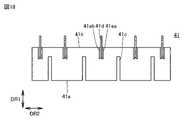
- FIG. 30 is a perspective view of the third partition plate 43 included in the circuit device 400.
- a circuit device 400 includes a circuit component 10 (capacitor 10a), a heat sink 30, a plurality of first partition plates 41, a plurality of second partition plates 42, an adhesive 50 , a heat transfer member 51 , a heat transfer member 52 , and a substrate 60 .
- the first partition plates 41 located other than the two ends in the third direction DR3 are the third partition plates 43 .
- the configuration of circuit device 400 is common to the configuration of circuit device 100 .
- the third partition plate 43 has a support portion 43g.
- the support portion 43g is arranged at the fifth end 43a.
- the third partition plate 43 is in contact with the upper surface 30a at the support portion 43g.
- the configuration of circuit device 400 differs from that of circuit device 100 .
- the third partition plate 43 having the support portion 43g is formed by, for example, forming the third insertion port 43c and then bending the fifth end 43a side by press working.
- the method of forming the third partition plate 43 having the support portion 43g is not limited to this.
- the third partition plate 43 having the support portion 43g may be formed by pressing or extruding a sheet metal having the support portion 43g and then punching or cutting to form the third insertion port 43c. .
- the third partition plate 43 having the support portion 43g may be formed by casting such as die casting.
- the third partition plate 43 having the support portion 43g may be formed by bonding a plurality of members by brazing, caulking, or the like, or by bonding with an adhesive.
- the contact area between the third partition plate 43 and the upper surface 30a is larger than in the circuit device 100. Therefore, in the circuit device 400 , the contact thermal resistance value between the third partition plate 43 and the upper surface 30 a is smaller than in the circuit device 100 .
- the temperature rise of the third partition plate 43 which receives a large amount of heat from the capacitor 10a, can be further suppressed, and the temperature rise of the circuit device 400 as a whole can be suppressed.
- the capacitor 10a between the adjacent first partition plate 41 and the third partition plate 43 and the capacitor 10a between the two adjacent third partition plates 43 can reduce the temperature gradient between
- circuit device 400A (hereinafter referred to as "circuit device 400A") according to a modification will be described.
- FIG. 31 is a cross-sectional view of the circuit device 400A.
- FIG. 32 is a perspective view of the third partition plate 43 included in the circuit device 400A.
- FIG. 31 shows a cross section of the circuit device 400A at a position corresponding to XXIX-XXIX in FIG.
- the thickness of the third partition plate 43 in the third direction DR3 is smaller than in the circuit device 400.
- the thickness of the third partition plate 43 in the third direction DR3 is equal to the thickness of the first partition plate 41 in the third direction DR3.
- the weight of the circuit device 400A can be reduced.
- the value of R a in Equation 1 is large. value is smaller. Therefore, in the circuit device 400A, the value of ⁇ t in Equation 1, that is, the temperature rise of the third partition plate 43 is suppressed.
- circuit device 500 A circuit device (hereinafter referred to as "circuit device 500") according to Embodiment 5 will be described. Differences from circuit device 100 will be mainly described below, and redundant description will not be repeated.
- circuit device 500 (Configuration of circuit device 500) The configuration of the circuit device 500 will be described below.
- FIG. 33 is an exploded perspective view of the circuit device 500.
- FIG. 34 is a cross-sectional view along XXXIV-XXXIV in FIG. 33.
- FIG. 35 is a perspective view of the first partition plate 41 included in the circuit device 500.
- FIG. 36 is a perspective view of the second partition plate 42 included in the circuit device 500.
- FIG. 37 is a perspective view of the third partition plate 43 included in the circuit device 500.
- a circuit device 500 includes a circuit component 10 (capacitor 10a), a heat sink 30, a plurality of first partition plates 41, a plurality of second partition plates 42, and an adhesive 50. , a heat transfer member 51 , a heat transfer member 52 , and a substrate 60 .
- the first partition plates 41 located other than the two ends in the third direction DR3 are the third partition plates 43 .
- the configuration of circuit device 500 is common to the configuration of circuit device 100 .
- the third partition plate 43 has a radiator plate 43h.
- the heat sink 43h extends in the third direction DR3.
- 43 h of heat sinks are in the both ends of the 3rd partition plate 43 in 2nd direction DR2.
- a plurality of fourth insertion openings 43i are formed in the sixth end 43b of the heat sink 43h.
- the fourth insertion port 43i extends toward the fifth end 43a.
- the multiple fourth insertion ports 43i are arranged at intervals in the third direction DR3.
- the first insertion port 41c is inserted into the fourth insertion port 43i.
- the configuration of circuit device 500 differs from that of circuit device 100 .
- the third partition plate 43 having the heat sink 43h is formed by, for example, forming a sheet metal having the heat sink 43h by extrusion, and then punching or cutting to form the third insertion opening 43c and the fourth insertion opening 43i. It is formed.
- the third partition plate 43 having the heat sink 43h may be formed by forming a sheet metal having the third insertion port 43c and the fourth insertion port 43i into a U-shape by pressing, and combining the U-shaped sheet metal. .
- the third partition plate 43 having the heat sink 43h may be formed by casting such as die casting.
- the third partition plate 43 having the heat dissipation plate 43h is prepared by punching sheet metal to prepare the heat dissipation plate 43h and the remainder of the third partition plate 43 as separate members, which are integrated by brazing, caulking, adhesion, or the like. may be formed by
- a plurality of fins may be formed on the heat sink 43h to improve heat dissipation.
- the fin extends in the first direction DR1.
- the plurality of fins are spaced apart in the third direction DR3.
- the third partition plate 43 having the heat sink 43h on which the fins are formed is formed by extrusion along the extending direction of the fins (first direction DR1).
- the contact area between the third partition plate 43 and the upper surface 30a is increased because the third partition plate 43 has the heat sink 43h.
- Rb in Equation 1 becomes smaller, the temperature rise of the third partition plate 43 ( ⁇ t in Equation 1) becomes smaller, and the temperature rise of the circuit device 500 as a whole is suppressed.
- the heat generated in the capacitor 10a passes through the side surface (the lead wire 10ab) of the capacitor 10a, the heat transfer member 52, and the third partition plate 43 to reach the heat sink 43h. (hereinafter referred to as "sixth heat dissipation path").
- the heat sink 43h is formed with fins, the cooling efficiency of the heat sink 43h is improved, so that the heat dissipation from the sixth heat dissipation path can be further improved.
- circuit device 600 A circuit device (hereinafter referred to as "circuit device 600") according to Embodiment 6 will be described. Differences from circuit device 100 will be mainly described below, and redundant description will not be repeated.
- circuit device 600 (Configuration of circuit device 600) The configuration of the circuit device 600 will be described below.
- FIG. 38 is an exploded perspective view of the circuit device 600.
- FIG. FIG. 39 is a cross-sectional view along XXXIX-XXXIX in FIG. 40 is a perspective view of the third partition plate 43 included in the circuit device 600.
- FIG. 40 a circuit device 600 has a circuit component 10 (capacitor 10a), a heat sink 30, a plurality of first partitions 41, and a plurality of second partitions 42.
- Circuit device 600 further includes adhesive 50 , heat transfer member 51 , heat transfer member 52 , and substrate 60 .
- the first partition plates 41 located other than the two ends in the third direction DR3 are the third partition plates 43 .
- the configuration of circuit device 600 is common to the configuration of circuit device 100 .
- the circuit device 600 further has a bottom plate 43j.
- the bottom plate 43j is between two adjacent third partition plates 43 and is in contact with the upper surface 30a.
- the configuration of circuit device 600 differs from that of circuit device 100 .
- the bottom plate 43j and the two adjacent third partition plates 43 may be one member.
- the two third partition plates 43 integrated by the bottom plate 43j are formed, for example, by punching a sheet metal to form the third insertion port 43c and then pressing.
- the two third partition plates 43 integrated by the bottom plate 43j may be formed by stamping or cutting to form the third insertion port 43c after pressing.
- the two third partition plates 43 integrated by the bottom plate 43j may be formed by casting such as die casting.
- the two third partition plates 43 integrated by the bottom plate 43j may be formed by separately forming the bottom plate 43j and the two third partition plates 43 and integrating them by brazing, caulking, adhesion, or the like. good.
- the third partition plate 43 since the third partition plate 43 has the bottom plate 43j, the contact area between the third partition plate 43 and the upper surface 30a is increased. As a result, Rb in Equation 1 becomes smaller, so the temperature rise of the third partition plate 43 ( ⁇ t in Equation 1) becomes smaller, and the temperature rise of the circuit device 600 as a whole is suppressed. Further, in the circuit device 600, since the temperature rise of the third partition plate 43 can be further suppressed, the capacitor 10a between the adjacent first partition plate 41 and the third partition plate 43 and the two adjacent third partition plates 41 and 43 The temperature gradient between the partition plates 43 and the capacitor 10a can be further reduced.
- the temperature difference between the two adjacent third partition plates 43 can be reduced. Therefore, according to the circuit device 600, the temperature distribution in the capacitor 10a between the two adjacent third partition plates 43 can be made uniform.
- circuit device 700 A circuit device (hereinafter referred to as "circuit device 700") according to Embodiment 7 will be described. Differences from circuit device 100 will be mainly described below, and redundant description will not be repeated.
- FIG. 41 is an exploded perspective view of the circuit device 700.
- FIG. 42 is a plan view of the first partition plate 41 included in the circuit device 700.
- FIG. 43 is a plan view of the second partition plate 42 included in the circuit device 700.
- FIG. 44 is a plan view of the third partition plate 43 included in the circuit device 700.
- a circuit device 700 includes a circuit component 10 (capacitor 10a), a heat sink 30, a plurality of first partition plates 41, a plurality of second partition plates 42, an adhesive 50 , a heat transfer member 51 , a heat transfer member 52 , and a substrate 60 .
- the first partition plates 41 located other than the two ends in the third direction DR3 are the third partition plates 43 .
- the configuration of circuit device 700 is common to the configuration of circuit device 100 .
- the first partition plate 41 is not formed with the first insertion port 41c
- the third partition plate 43 is not formed with the third insertion port 43c.
- the second partition plate 42 is formed with a plurality of second insertion openings 42k spaced apart in the third direction DR3.
- the second receptacle 42k extends from the third end 42a toward the fourth end 42b.
- the second insertion port 42k penetrates the second partition plate 42 along the thickness direction.
- the second insertion port 42 k is inserted into the first partition plate 41 and the third partition plate 43 .
- the configuration of circuit device 700 differs from that of circuit device 100 .
- the first partition plate 41 does not have the first insertion port 41c
- the third partition plate 43 does not have the third insertion port 43c.
- the contact area between and the contact area between the third partition plate 43 and the upper surface 30a are increased.
- the contact thermal resistance between the first partition plate 41 and the upper surface 30a and the contact thermal resistance between the third partition plate 43 and the upper surface 30a are reduced, and the temperature rise of the circuit device 700 as a whole is suppressed.
- the first partition plate 41 is not formed with the first insertion port 41c
- the third partition plate 43 is not formed with the third insertion port 43c. It is possible to move along the two directions DR2 and to increase or decrease the number of second partition plates 42 used. As a result, according to the circuit device 700, it is not necessary to change the shape of the first partition plate 41, the second partition plate 42, and the third partition plate 43 even when manufacturing the circuit device 700 with different numbers or sizes of the capacitors 10a. , the design of the first partition plate 41, the second partition plate 42 and the third partition plate 43 according to the number or size of the capacitors 10a to be used can be eliminated.
- circuit device 700A A circuit device 700 (hereinafter referred to as “circuit device 700A”) according to Modification 1 will be described.
- FIG. 45 is an exploded perspective view of the circuit device 700A.
- FIG. 46 is a plan view of the first partition plate 41 included in the circuit device 700A.
- FIG. 47 is a plan view of the second partition plate 42 included in the circuit device 700A.
- FIG. 48 is a plan view of the third partition plate 43 included in the circuit device 700A.
- the first partition plate 41 is formed with a plurality of first insertion openings 41k spaced apart in the second direction DR2.
- the first insertion port 41k extends from the second end 41b toward the first end 41a.
- the first insertion port 41k penetrates the first partition plate 41 along the thickness direction.
- a plurality of third insertion openings 43k are formed in the third partition plate 43 at intervals in the second direction DR2.
- the third insertion port 43k extends from the sixth end 43b toward the fifth end 43a.
- the third insertion port 43k penetrates the third partition plate 43 along the thickness direction.
- the second partition plate 42 is not formed with the second insertion port 42k. The second partition plate 42 is inserted into the first insertion port 41k and the third insertion port 43k.
- the first partition plate 41 is not provided with the first insertion port 41c
- the third partition plate 43 is not provided with the third insertion port 43c.
- the contact area between the partition plate 41 and the upper surface 30a and the contact area between the third partition plate 43 and the upper surface 30a are increased.
- the contact thermal resistance between the first partition plate 41 and the upper surface 30a and the contact thermal resistance between the third partition plate 43 and the upper surface 30a are reduced, thereby suppressing the temperature rise of the circuit device 700A as a whole.
- the second partition plate 42 is not formed with the second insertion port 42c.
- the number of partition plates 41 and third partition plates 43 used can be increased or decreased.
- the design of the first partition plate 41, the second partition plate 42 and the third partition plate 43 according to the number or size of the capacitors 10a to be used can be eliminated.
- circuit device 700B A circuit device 700 (hereinafter referred to as “circuit device 700B”) according to modification 2 will be described.
- FIG. 49 is an exploded perspective view of the circuit device 700B.
- the circuit device 700B some of the plurality of capacitors 10a are replaced with inductors 10b, contactors 10c, discharge resistors 10d, charge resistors 10e, and voltage dividing resistors 10f.
- the second partition plate 42 is moved along the second direction DR2 according to the sizes of the inductor 10b, the contactor 10c, the discharge resistor 10d, the charge resistor 10e, and the voltage dividing resistor 10f. It is possible to increase or decrease the number of plates 42 used. Therefore, according to the circuit device 700B, it is possible to improve the heat dissipation of the inductor 10b, the contactor 10c, the discharge resistor 10d, the charge resistor 10e, and the voltage dividing resistor 10f.
Landscapes
- Engineering & Computer Science (AREA)
- Power Engineering (AREA)
- Microelectronics & Electronic Packaging (AREA)
- Manufacturing & Machinery (AREA)
- Cooling Or The Like Of Electrical Apparatus (AREA)
Priority Applications (2)
| Application Number | Priority Date | Filing Date | Title |
|---|---|---|---|
| JP2023530340A JP7634674B2 (ja) | 2021-06-22 | 2022-06-14 | 回路装置 |
| US18/559,943 US20240244754A1 (en) | 2021-06-22 | 2022-06-14 | Circuit Device |
Applications Claiming Priority (2)
| Application Number | Priority Date | Filing Date | Title |
|---|---|---|---|
| JP2021103423 | 2021-06-22 | ||
| JP2021-103423 | 2021-06-22 |
Publications (1)
| Publication Number | Publication Date |
|---|---|
| WO2022270353A1 true WO2022270353A1 (ja) | 2022-12-29 |
Family
ID=84544331
Family Applications (1)
| Application Number | Title | Priority Date | Filing Date |
|---|---|---|---|
| PCT/JP2022/023770 Ceased WO2022270353A1 (ja) | 2021-06-22 | 2022-06-14 | 回路装置 |
Country Status (3)
| Country | Link |
|---|---|
| US (1) | US20240244754A1 (https=) |
| JP (1) | JP7634674B2 (https=) |
| WO (1) | WO2022270353A1 (https=) |
Citations (5)
| Publication number | Priority date | Publication date | Assignee | Title |
|---|---|---|---|---|
| JPH10116756A (ja) * | 1996-10-11 | 1998-05-06 | Honda Motor Co Ltd | コンデンサ |
| JP2000195748A (ja) * | 1998-12-25 | 2000-07-14 | Matsushita Electric Ind Co Ltd | コンデンサ |
| JP2014116400A (ja) * | 2012-12-07 | 2014-06-26 | Toyota Motor Corp | コンデンサモジュール |
| WO2016117441A1 (ja) * | 2015-01-22 | 2016-07-28 | カルソニックカンセイ株式会社 | コンデンサ構造 |
| JP2019179856A (ja) * | 2018-03-30 | 2019-10-17 | 日本ケミコン株式会社 | 蓄電デバイスモジュール及び蓄電デバイスホルダー |
-
2022
- 2022-06-14 JP JP2023530340A patent/JP7634674B2/ja active Active
- 2022-06-14 WO PCT/JP2022/023770 patent/WO2022270353A1/ja not_active Ceased
- 2022-06-14 US US18/559,943 patent/US20240244754A1/en active Pending
Patent Citations (5)
| Publication number | Priority date | Publication date | Assignee | Title |
|---|---|---|---|---|
| JPH10116756A (ja) * | 1996-10-11 | 1998-05-06 | Honda Motor Co Ltd | コンデンサ |
| JP2000195748A (ja) * | 1998-12-25 | 2000-07-14 | Matsushita Electric Ind Co Ltd | コンデンサ |
| JP2014116400A (ja) * | 2012-12-07 | 2014-06-26 | Toyota Motor Corp | コンデンサモジュール |
| WO2016117441A1 (ja) * | 2015-01-22 | 2016-07-28 | カルソニックカンセイ株式会社 | コンデンサ構造 |
| JP2019179856A (ja) * | 2018-03-30 | 2019-10-17 | 日本ケミコン株式会社 | 蓄電デバイスモジュール及び蓄電デバイスホルダー |
Also Published As
| Publication number | Publication date |
|---|---|
| JP7634674B2 (ja) | 2025-02-21 |
| US20240244754A1 (en) | 2024-07-18 |
| JPWO2022270353A1 (https=) | 2022-12-29 |
Similar Documents
| Publication | Publication Date | Title |
|---|---|---|
| US6765285B2 (en) | Power semiconductor device with high radiating efficiency | |
| US3359461A (en) | Modular circuit package | |
| US9226430B2 (en) | Power semiconductor module | |
| JP7154428B2 (ja) | 電力変換装置および電力変換装置の製造方法 | |
| EP3580789B1 (en) | Thermoelectric module | |
| TW200810677A (en) | Electronic element module | |
| CN112119579B (zh) | 功率转换装置 | |
| GB2471497A (en) | Double sided multi-layer metal substrate PCB with SMD components mounted to top traces and lead wire components mounted to opposite side for heat dissipation | |
| JP6999777B1 (ja) | 電力変換装置 | |
| JP5236178B2 (ja) | 電子回路装置 | |
| JP7634673B2 (ja) | 回路装置 | |
| JPS5893264A (ja) | デバイスの冷却装置 | |
| JP2012190955A (ja) | 射出成型基板 | |
| US20040227230A1 (en) | Heat spreaders | |
| JP7634674B2 (ja) | 回路装置 | |
| WO2020080248A1 (ja) | 回路構造体及び電気接続箱 | |
| JP4522271B2 (ja) | 電子装置及びこれに用いられる放熱板アセンブリ | |
| JP6979997B2 (ja) | 電力用半導体装置 | |
| JP5621812B2 (ja) | 半導体装置 | |
| JP2003188563A (ja) | 電子制御装置 | |
| WO2023053967A1 (ja) | 電力変換装置及び電力変換装置の製造方法 | |
| JPH06507044A (ja) | 液冷式装置内の発熱器の配列構造 | |
| JP2001237368A (ja) | パワーモジュール | |
| JP2009188192A (ja) | 回路装置 | |
| CN212992673U (zh) | 一种控制器、汽车电子水泵及汽车电子压缩机 |
Legal Events
| Date | Code | Title | Description |
|---|---|---|---|
| 121 | Ep: the epo has been informed by wipo that ep was designated in this application |
Ref document number: 22828270 Country of ref document: EP Kind code of ref document: A1 |
|
| WWE | Wipo information: entry into national phase |
Ref document number: 2023530340 Country of ref document: JP |
|
| WWE | Wipo information: entry into national phase |
Ref document number: 18559943 Country of ref document: US |
|
| NENP | Non-entry into the national phase |
Ref country code: DE |
|
| 122 | Ep: pct application non-entry in european phase |
Ref document number: 22828270 Country of ref document: EP Kind code of ref document: A1 |