WO2022270299A1 - 積層セラミック電子部品およびその製造方法 - Google Patents
積層セラミック電子部品およびその製造方法 Download PDFInfo
- Publication number
- WO2022270299A1 WO2022270299A1 PCT/JP2022/023004 JP2022023004W WO2022270299A1 WO 2022270299 A1 WO2022270299 A1 WO 2022270299A1 JP 2022023004 W JP2022023004 W JP 2022023004W WO 2022270299 A1 WO2022270299 A1 WO 2022270299A1
- Authority
- WO
- WIPO (PCT)
- Prior art keywords
- external electrode
- rod
- ceramic
- cut
- layer
- Prior art date
- Legal status (The legal status is an assumption and is not a legal conclusion. Google has not performed a legal analysis and makes no representation as to the accuracy of the status listed.)
- Ceased
Links
Images















Classifications
-
- H—ELECTRICITY
- H01—ELECTRIC ELEMENTS
- H01G—CAPACITORS; CAPACITORS, RECTIFIERS, DETECTORS, SWITCHING DEVICES, LIGHT-SENSITIVE OR TEMPERATURE-SENSITIVE DEVICES OF THE ELECTROLYTIC TYPE
- H01G4/00—Fixed capacitors; Processes of their manufacture
- H01G4/002—Details
- H01G4/224—Housing; Encapsulation
-
- H—ELECTRICITY
- H01—ELECTRIC ELEMENTS
- H01C—RESISTORS
- H01C7/00—Non-adjustable resistors formed as one or more layers or coatings; Non-adjustable resistors made from powdered conducting material or powdered semi-conducting material with or without insulating material
- H01C7/02—Non-adjustable resistors formed as one or more layers or coatings; Non-adjustable resistors made from powdered conducting material or powdered semi-conducting material with or without insulating material having positive temperature coefficient
-
- H—ELECTRICITY
- H01—ELECTRIC ELEMENTS
- H01C—RESISTORS
- H01C7/00—Non-adjustable resistors formed as one or more layers or coatings; Non-adjustable resistors made from powdered conducting material or powdered semi-conducting material with or without insulating material
- H01C7/04—Non-adjustable resistors formed as one or more layers or coatings; Non-adjustable resistors made from powdered conducting material or powdered semi-conducting material with or without insulating material having negative temperature coefficient
-
- H—ELECTRICITY
- H01—ELECTRIC ELEMENTS
- H01C—RESISTORS
- H01C7/00—Non-adjustable resistors formed as one or more layers or coatings; Non-adjustable resistors made from powdered conducting material or powdered semi-conducting material with or without insulating material
- H01C7/10—Non-adjustable resistors formed as one or more layers or coatings; Non-adjustable resistors made from powdered conducting material or powdered semi-conducting material with or without insulating material voltage responsive, i.e. varistors
-
- H—ELECTRICITY
- H01—ELECTRIC ELEMENTS
- H01F—MAGNETS; INDUCTANCES; TRANSFORMERS; SELECTION OF MATERIALS FOR THEIR MAGNETIC PROPERTIES
- H01F17/00—Fixed inductances of the signal type
-
- H—ELECTRICITY
- H01—ELECTRIC ELEMENTS
- H01G—CAPACITORS; CAPACITORS, RECTIFIERS, DETECTORS, SWITCHING DEVICES, LIGHT-SENSITIVE OR TEMPERATURE-SENSITIVE DEVICES OF THE ELECTROLYTIC TYPE
- H01G4/00—Fixed capacitors; Processes of their manufacture
- H01G4/002—Details
- H01G4/018—Dielectrics
- H01G4/06—Solid dielectrics
- H01G4/08—Inorganic dielectrics
- H01G4/12—Ceramic dielectrics
-
- H—ELECTRICITY
- H01—ELECTRIC ELEMENTS
- H01G—CAPACITORS; CAPACITORS, RECTIFIERS, DETECTORS, SWITCHING DEVICES, LIGHT-SENSITIVE OR TEMPERATURE-SENSITIVE DEVICES OF THE ELECTROLYTIC TYPE
- H01G4/00—Fixed capacitors; Processes of their manufacture
- H01G4/002—Details
- H01G4/018—Dielectrics
- H01G4/06—Solid dielectrics
- H01G4/08—Inorganic dielectrics
- H01G4/12—Ceramic dielectrics
- H01G4/1209—Ceramic dielectrics characterised by the ceramic dielectric material
- H01G4/1218—Ceramic dielectrics characterised by the ceramic dielectric material based on titanium oxides or titanates
- H01G4/1227—Ceramic dielectrics characterised by the ceramic dielectric material based on titanium oxides or titanates based on alkaline earth titanates
-
- H—ELECTRICITY
- H01—ELECTRIC ELEMENTS
- H01G—CAPACITORS; CAPACITORS, RECTIFIERS, DETECTORS, SWITCHING DEVICES, LIGHT-SENSITIVE OR TEMPERATURE-SENSITIVE DEVICES OF THE ELECTROLYTIC TYPE
- H01G4/00—Fixed capacitors; Processes of their manufacture
- H01G4/002—Details
- H01G4/228—Terminals
- H01G4/232—Terminals electrically connecting two or more layers of a stacked or rolled capacitor
-
- H—ELECTRICITY
- H01—ELECTRIC ELEMENTS
- H01G—CAPACITORS; CAPACITORS, RECTIFIERS, DETECTORS, SWITCHING DEVICES, LIGHT-SENSITIVE OR TEMPERATURE-SENSITIVE DEVICES OF THE ELECTROLYTIC TYPE
- H01G4/00—Fixed capacitors; Processes of their manufacture
- H01G4/002—Details
- H01G4/228—Terminals
- H01G4/232—Terminals electrically connecting two or more layers of a stacked or rolled capacitor
- H01G4/2325—Terminals electrically connecting two or more layers of a stacked or rolled capacitor characterised by the material of the terminals
-
- H—ELECTRICITY
- H01—ELECTRIC ELEMENTS
- H01G—CAPACITORS; CAPACITORS, RECTIFIERS, DETECTORS, SWITCHING DEVICES, LIGHT-SENSITIVE OR TEMPERATURE-SENSITIVE DEVICES OF THE ELECTROLYTIC TYPE
- H01G4/00—Fixed capacitors; Processes of their manufacture
- H01G4/002—Details
- H01G4/228—Terminals
- H01G4/248—Terminals the terminals embracing or surrounding the capacitive element, e.g. caps
-
- H—ELECTRICITY
- H01—ELECTRIC ELEMENTS
- H01G—CAPACITORS; CAPACITORS, RECTIFIERS, DETECTORS, SWITCHING DEVICES, LIGHT-SENSITIVE OR TEMPERATURE-SENSITIVE DEVICES OF THE ELECTROLYTIC TYPE
- H01G4/00—Fixed capacitors; Processes of their manufacture
- H01G4/30—Stacked capacitors
Definitions
- the present disclosure relates to a multilayer ceramic electronic component and a manufacturing method thereof.
- Patent Document 1 An example of conventional technology is described in Patent Document 1.
- a laminated ceramic electronic component of the present disclosure includes a substantially rectangular parallelepiped element component, a first external electrode, a second external electrode, and a protective layer.
- the element body component is formed by alternately laminating a plurality of ceramic layers and a plurality of internal electrode layers having different polarities. It has a face and a second face, a first end face and a second end face facing each other, and a first side face and a second side face facing each other.
- the plurality of internal electrode layers are exposed on the first side surface and the second side surface, and are exposed on either one of the first end surface and the second end surface according to polarity.
- the first external electrode is connected to the internal electrode layer exposed on the first end surface
- the second external electrode is connected to the internal electrode layer exposed on the second end surface.
- Each of the first external electrode and the second external electrode extends over at least one of the first surface and the second surface and is flush with the first side surface and the second side surface, respectively. It has one external electrode side surface and a second external electrode side surface.
- the protective layer contains a ceramic material and covers the first and second side surfaces and the first and second external electrode side surfaces of the first and second external electrodes.
- a mother laminated body in which a plurality of ceramic green sheets and a plurality of internal electrode layers are alternately laminated is cut at predetermined intervals, and the first surface and the second surface are cut.
- a first rod-shaped body having a surface, a first cut surface and a second cut surface is produced, and edges between the first surface and the second surface and the first cut surface and the second cut surface are formed.
- a body is prepared, and the second rod-shaped body is cut at predetermined intervals in a direction perpendicular to the longitudinal direction of the second rod-shaped body, and the plurality of internal electrode layers are exposed on the third cut surface and the fourth cut surface. and forming a protective layer containing a ceramic material on each of the third cut surface and the fourth cut surface.
- FIG. 1 is a perspective view showing an example of a laminated ceramic electronic component according to an embodiment of the present disclosure
- FIG. FIG. 2 is an exploded perspective view showing the multilayer ceramic electronic component of FIG. 1
- FIG. 3 is a cross-sectional view showing a base component of the multilayer ceramic electronic component cut along a cutting plane line AA in FIG. 2
- FIG. 3 is a photograph showing a part of the multilayer ceramic electronic component cut along the cutting plane line AA in FIG. 2.
- FIG. 1 is a perspective view showing a state in which a plurality of conventional laminated ceramic electronic components are mounted on a mounting substrate
- FIG. 2 is a perspective view showing a state in which a plurality of laminated ceramic electronic components of FIG. 1 are mounted on a mounting substrate;
- FIG. 5B is a cross-sectional view taken along the cutting plane line BB in FIG. 5A;
- FIG. 5C is a cross-sectional view cut along the cutting plane line CC of FIG. 5B;
- FIG. 4 is a perspective view showing an example of a laminated ceramic electronic component according to another embodiment of the present disclosure;
- FIG. 8 is an exploded perspective view showing the multilayer ceramic electronic component of FIG. 7;
- FIG. 10 is a perspective view showing an example of a laminated ceramic electronic component according to still another embodiment of the present disclosure;
- FIG. 10 is a cross-sectional view cut along a cutting plane line DD in FIG. 9;
- FIG. 3 is a perspective view showing a state in which a conductive paste is printed on a ceramic green sheet;
- FIG. 2 is an external view showing a state in which a plurality of ceramic green sheets on which conductive paste is printed are laminated.
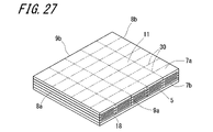
- FIG. 3 is a perspective view showing a mother laminate;
- FIG. 4 is a perspective view showing a state in which a first rod-shaped body obtained by cutting a mother laminate is chamfered;
- FIG. 4 is a perspective view showing a state in which a plurality of first rod-shaped bodies are rotated such that a first cut plane is positioned within a virtual plane;
- FIG. 5 is a diagram showing a state in which external electrode paste is applied to the first cut surface of the first rod;
- FIG. 4 is a perspective view showing a second rod-shaped body on which an external electrode base layer is formed;
- FIG. 11 is a perspective view showing a state in which the second rod-shaped body is cut;
- FIG. 10 is a perspective view showing a state in which the cut surfaces of the second base body parts cut into individual chips are arranged in a vertical direction;
- FIG. 10 is a cross-sectional view schematically showing a state in which ceramic paste is applied to the second base component;
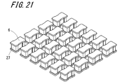
- FIG. 10 is a perspective view showing the state of the second element body part on which the protective layer is formed;
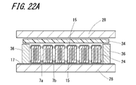
- FIG. 4 is a cross-sectional view schematically showing a state in which a plurality of second rod-shaped bodies are melt-fixed with a thermoplastic resin sheet to form an aggregate.
- FIG. 4 is a cross-sectional view schematically showing a state in which a plurality of second rod-shaped bodies are melt-fixed with a thermoplastic resin sheet to form an aggregate.
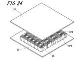
- FIG. 10 is a perspective view showing a state in which the assembly is cut to produce a third rod-shaped body;
- FIG. 4 is a perspective view showing a state in which a ceramic green sheet is arranged on a cut surface of a third rod;
- FIG. 4 is a perspective view showing a third rod-shaped body to which a ceramic green sheet is attached;
- FIG. 11 is a perspective view showing a state after firing of the third rod-shaped body to which the ceramic green sheet is attached;
- FIG. 4 is a perspective view showing a mother laminate laminated on a support sheet;
- FIG. 4 is a perspective view showing a state in which a first rod-shaped body obtained by cutting the base laminate together with the support sheet is chamfered.
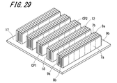
- FIG. 29 is a perspective view showing a state in which the first rod-shaped body of FIG. 28 is rotated so that the cut surface thereof is positioned vertically;
- FIG. 30 is a cross-sectional view showing a state in which an external electrode base layer is applied to the cut surface of the first rod-shaped body of FIG. 29;
- 31 is a perspective view showing a second rod-shaped body in which an external electrode base layer is formed on the first rod-shaped body of FIG. 30;
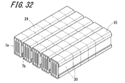
- FIG. FIG. 32 is a perspective view showing a state where the supporting sheet of the second rod-shaped body of FIG. 31 is peeled off;
- Patent Document 1 in order to improve the acquired capacitance per unit volume, which is the function of a multilayer ceramic capacitor, the side margins for protecting the internal electrodes are made thinner to increase the area ratio of the internal electrodes, and discloses that the external electrodes are not formed on the side surfaces of the element constituting the multilayer ceramic capacitor, thereby reducing the occurrence of leakage current between the external electrodes and the internal electrodes even if the side margin portions are made thin.
- the method for manufacturing a multilayer ceramic electronic component according to the present disclosure is not limited to the method for manufacturing a multilayer ceramic capacitor, and can be used to manufacture various multilayer ceramic electronic components such as a multilayer piezoelectric element, a multilayer thermistor element, a multilayer chip coil, and a ceramic multilayer substrate. It can also be applied to manufacturing methods. Except for the photograph shown in FIG. 4, the figures referred to below are schematic, and the positions, dimensional ratios, etc. of the components of the multilayer ceramic electronic component are not necessarily shown accurately.
- FIG. 1 is a perspective view showing an example of a laminated ceramic electronic component according to one embodiment of the present disclosure
- FIG. 2 is an exploded perspective view showing the laminated ceramic electronic component of FIG.
- FIG. 3 is a cross-sectional view showing a base component of a laminated ceramic electronic component cut along the cutting plane line AA in FIG. 2
- FIG. 4 is a laminated ceramic electronic component cut along the cutting plane line AA in FIG. It is a photograph which shows a part of components.
- FIG. 4 shows a portion near the end surface of the elemental component and a portion of the external electrode on the elemental component side.
- FIG. 5A is a perspective view showing a state in which a plurality of conventional multilayer ceramic electronic components are mounted on a mounting substrate
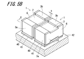
- FIG. 5B is a perspective view showing a state in which a plurality of the multilayer ceramic electronic components of FIG. 1 are mounted on the mounting substrate.
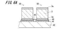
- 6A is a sectional view cut along the section line BB in FIG. 5A
- FIG. 6B is a sectional view cut along the section line CC in FIG. 5B.
- the laminated ceramic electronic component 1 of this embodiment includes, for example, a base component 2, first external electrodes 3a and second external electrodes 3b, and a protective layer 6, as shown in FIG.
- the laminated ceramic electronic component 1 is sometimes referred to as a laminated ceramic capacitor 1 below.
- the base component 2 has a substantially rectangular parallelepiped shape, for example, as shown in FIG.
- the element component 2 is a laminate in which a plurality of dielectric ceramic layers (hereinafter also simply referred to as ceramic layers) 4 and a plurality of internal electrode layers 5 having different polarities are alternately laminated.
- a ceramic layer 4 is interposed between a pair of internal electrode layers 5 provided.
- the element body component 2 has a first surface 7a and a second surface 7b facing each other in the stacking direction of the plurality of ceramic layers 4 and the plurality of internal electrode layers 5 .
- the base component 2 also has a first end face 8a and a second end face 8b facing each other, and a first side face 9a and a second side face 9b facing each other.
- the 1st surface 7a and the 2nd surface 7b may be named generically as the main surface 7a and the main surface 7b.
- the first end surface 8a and the second end surface 8b may be collectively called the end surface 8a and the end surface 8b
- the first side surface 9a and the second side surface 9b may be collectively called the side surface 9a and the side surface 9b.
- the ceramic layer 4 may contain a ceramic material such as BaTiO 3 (barium titanate).
- the ceramic layer 4 may be made mainly of barium titanate.
- the internal electrode layers 5 may contain metals such as Ni (nickel), Pd (palladium), Cu (copper), Ag (silver), or alloys thereof.
- the internal electrode layers 5 may be made mainly of nickel or a nickel alloy.
- the plurality of internal electrode layers 5 are exposed on both the first side surface 9a and the second side surface 9b. Furthermore, the plurality of internal electrode layers 5 are exposed on either one of the first end surface 8a and the second end surface 8b according to polarity. In other words, each of the plurality of internal electrode layers 5 is exposed to the first end face 8a or the second end face 8b according to the polarity given to the internal electrode layer 5. As shown in FIG.
- the first external electrode 3a is positioned on one of the first end surface 8a and the second end surface 8b (the first end surface 8a), and the internal electrode layer 5 exposed on the end surface. It is connected.
- the second external electrode 3b is located on the other end surface (second end surface 8b) of the first end surface 8a and the second end surface 8b, for example, as shown in FIG. It is connected.
- the first external electrode 3a extends from the first end surface 8a to at least one of the first surface 7a and the second surface 7b.
- the second external electrode 3b extends from the second end surface 8b to at least one of the first surface 7a and the second surface 7b.
- the first external electrode 3a and the second external electrode 3b extend a predetermined distance in a direction orthogonal to the end surfaces 8a and 8b.
- 1 and 2 show an example in which the first external electrode 3a and the second external electrode 3b extend from the end surfaces 8a and 8b to both the main surfaces 7a and 7b.
- Each of the first external electrode 3a and the second external electrode 3b has a first external electrode side surface 3c and a second external electrode side surface 3d.
- the first external electrode side surface 3c and the second external electrode side surface 3d of the first external electrode 3a are flush with the first side surface 9a and the second side surface 9b of the base component 2, respectively.
- the first external electrode side surface 3c and the second external electrode side surface 3d of the second external electrode 3b are flush with the first side surface 9a and the second side surface 9b of the base component 2, respectively.
- the protective layer 6 contains an insulating ceramic material.
- the protective layer 6 may contain a ceramic material such as barium titanate.
- the protective layer 6 may be mainly composed of barium titanate.
- the protective layer 6 covers the side surfaces 9a and 9b of the base component 2, the external electrode side surfaces 3c and 3d of the first external electrode 3a, and the external electrode side surfaces 3c and 3d of the second external electrode 3b. ing.
- the first external electrode side surface 3c and the second external electrode side surface 3d of the first external electrode 3a are flush with the first side surface 9a and the second external electrode side surface 9b, respectively, and the second external electrode side surface 3d of the second external electrode 3b is flat.
- the first external electrode side surface 3c and the second external electrode side surface 3d are flush with the first side surface 9a and the second side surface 9b, respectively. Therefore, it is possible to simultaneously form the protective layer 6 on the base component 2, the first external electrode 3a and the second external electrode 3b, which are made of different materials, easily and accurately.
- the first external electrode 3a extends from the first end surface 8a to both the first surface 7a and the second surface 7b
- the second external electrode 3b extends from the second end surface 8b to both the first surface 7a and the second surface 7b.
- the protective layer 6 has a substantially H-shaped shape when viewed from a direction orthogonal to the side surfaces 9a and 9b, as shown in FIGS. 1 and 2, for example.
- the first external electrode 3a extends from the first end surface 8a to one of the first surface 7a and the second surface 7b
- the second external electrode 3b extends from the second end surface 8b to the first surface 7a and the second surface 7b.
- the protective layer 6 When extending over one of them, the protective layer 6 has a substantially U-shaped shape when viewed from a direction orthogonal to the side surfaces 9a and 9b.
- the boundary between the base component 2 and the protective layer 6 is indicated by a chain double-dashed line for convenience of explanation, but the actual boundary does not appear clearly.
- the side surfaces 9a, 9b, the external electrode side surfaces 3c, and the external electrode side surfaces 3d are covered with the protective layer 6 containing an insulating ceramic material.
- the protective layer 6 containing an insulating ceramic material is mounted on a circuit board, a plurality of laminated ceramic electronic components 1 can be arranged close to each other while reducing short circuits between the laminated ceramic electronic components 1 . Therefore, the multilayer ceramic capacitor 1 of this embodiment can be mounted on a circuit board with high density.
- the area from the side edge of the internal electrode layer 5 to the side of the element component is called a side margin.
- the protective layer 6 substantially functions as a side margin, but the thickness of the protective layer 6 can be reduced (for example, 30 ⁇ m or less). Therefore, in the multilayer ceramic electronic component 1, the area ratio of the internal electrode layers 5 can be increased to increase the acquired capacitance.
- the area ratio of the internal electrode layers 5 refers to the number of internal electrode layers with respect to the area of the base component 2 and the protective layer 6 when viewed in plan (when viewed in a direction orthogonal to the main surfaces 7a and 7b). 5 may be the ratio of the areas of the overlapping portions.
- the thickness of the protective layer 6 may be 5 ⁇ m or more and 30 ⁇ m or less.
- Each of the first external electrode 3 a and the second external electrode 3 b may have an external electrode base layer 15 in contact with the base component 2 .
- the base component 2 may have chamfered edges between the main surfaces 7a, 7b and the end surfaces 8a, 8b. If the ridges between the main surfaces 7a, 7b and the end surfaces 8a, 8b are not chamfered, the thickness of the external electrode base layer 15 does not exceed the thickness of the main surfaces 7a, 8b when forming the external electrode base layer 15. The corners connecting the main surface 7b and the end surfaces 8a and 8b are likely to be thinned.
- the base component 2 may have a chamfering distance a of 3 ⁇ m or more, as shown in FIG. 3, for example.
- the chamfering distance a refers to the shortest distance from the line of intersection of the extended surfaces of the main surfaces 7a and 7b and the extended surfaces of the end surfaces 8a and 8b to the surface of the base component 2. .
- Each of the first external electrode 3a and the second external electrode 3b may have a plated outer layer 16 located on the side of the external electrode base layer 15 opposite to the base component 2 side.
- the multilayer ceramic capacitor 1 is mounted on the circuit board 42 by, for example, joining the external electrodes 3 to electrode pads 41 provided on the circuit board 42 using a conductive joining material such as solder 40 (Fig. 5B, 6B). Since the external electrodes 3 have the plated outer layers 16, corrosion of the external electrodes 3 can be reduced, and the bonding between the multilayer ceramic capacitor 1 and the circuit board 42 by the conductive bonding material can be strengthened.
- the external electrode base layer 15 may contain a ceramic material and a conductive metal material.
- the ceramic material of the external electrode base layer 15 may have the same or similar component as the main component of the ceramic layer 4 and the main component of the protective layer 6 .
- the conductive metal material of the external electrode base layer 15 may have the same or similar component as the main component of the internal electrode layer 5 . In this case, as will be described later, it is possible to improve the bonding strength between the external electrode base layer 15 and the base component 2 and the protective layer 6, while reducing the decrease in conductivity of the external electrode base layer 15. Capacitor reliability can be improved.
- the meaning that the main components are the same or similar, which will also be described below, will be explained.
- the main component refers only to the components of the inorganic material, even if it is composed of inorganic and organic materials, and the inorganic material portion of the ceramic or electrode is When it is composed of a single component or multiple components, the component that accumulates 80% from the component with the highest ratio is called the main component, which means that the constituent components are the same. Although they are the same, variations in composition ratio, particle size, etc. are allowed between them, so the expression that the main components are the same or similar is used.
- the external electrode base layer 15 may be made by firing a conductive paste obtained by mixing a raw material powder made of dielectric ceramic powder and conductive metal powder with a binder or the like.
- the conductive paste that forms the external electrode base layer 15 may be applied to the base component 2 before firing the base component 2 and fired together with the base component 2 .
- the plating outer layer 16 may be formed on the surface of the external electrode base layer 15 opposite to the side of the base component 2 after firing the base component 2 and the external electrode base layer 15 .
- the external electrode base layer 15 or the plated outer layer 16 may be a single layer or multiple layers.
- the plated outer layer 16 may have a lower layer of Ni on the side of the external electrode base layer 15 and a surface layer of Sn.
- a conductive resin layer may be provided.
- FIG. 4 is a photograph showing the state of joints between the end faces 8a and 8b of the base component 2 and the external electrode base layers 15 of the first external electrodes 3a and the second external electrodes 3b.
- the photograph of FIG. 4 is obtained by observing the cross section of the multilayer ceramic capacitor 1 using a scanning electron microscope.
- the external electrode base layer 15 forms a mesh-like matrix consisting of a metal phase 45 (white area in FIG. 4) and a ceramic phase 46 (black area in FIG. 4) in a cross-sectional view.
- the internal electrode layers 5 of the base component 2 are formed in layers up to the end surfaces 8a and 8b, and are sintered and bonded to the metal phase 45 of the external electrode base layer 15. As shown in FIG.
- the dielectric ceramic layer 4 of the base component 2 is sinter-bonded to the ceramic phase 46 of the external electrode base layer 15 at the end faces 8a and 8b. Although not shown, in the same way as the sintering bonding between the dielectric ceramic layer 4 and the external electrode base layer 15 shown in FIG. It is sintered and bonded.
- the ceramic of the base component 2 and the ceramic of the external electrode base layer 15 are sintered and bonded at the end faces 8a and 8b, the ceramic region of the base component 2 and the amorphous ceramic region of the external electrode base layer 15 are integrated. As a result, the external electrode base layer 15 is firmly bonded to the base component 2 . Similarly, between the external electrode base layer 15 and the protective layer 6, a strong bond can be realized by the sinter-bonded interfacial ceramic.
- the external electrode base layer 15 is composed of a ceramic material and a conductive metal material.
- the ceramic material of the external electrode base layer 15 may have the same or similar component as the main component of the ceramic layer 4 and the protective layer 6 of the base component 2 .
- the conductive metal material of the external electrode base layer 15 may have the same or similar component as the main component of the internal electrode layer 5 .
- Element part 2, first external electrode 3a and second external electrode 3b attached to element part 2, and protective layer 6 attached to element part 2 and first external electrode 3a and second external electrode 3b may be formed simultaneously by firing.
- these components are firmly fixed to each other, It becomes possible to obtain the predetermined function of the multilayer ceramic capacitor 1 . Since ceramic materials having the same or similar main components have similar sintering temperatures, they start sintering at the same time to bond the ceramic particles together.
- the sintering bond between the metal particles contained in the internal electrode layer 5 and the metal particles contained in the external electrode base layer 15 is formed at the bonding portions on the end faces 8a and 8b of the base component 2. occur.
- the metal particles of the internal electrode layers 5 and the metal particles of the external electrode base layer 15 may be the same or similar materials that exhibit substantially the same behavior during firing.
- the ratio of the metal phase 45 and the ceramic phase 46 in the external electrode base layer 15 may be controlled.
- the ratio between the metal phase 45 and the ceramic phase 46 may be, for example, the ratio between the area of the metal phase 45 and the area of the ceramic phase 46 when the external electrode base layer 15 is viewed in cross section.
- the ratio of the ceramic phase 46 is large, the bonding strength between the external electrode base layer 15 and the base component 2 and the protective layer 6 can be improved, but the conductivity of the external electrode base layer 15 is lowered, and the internal electrode layer 5, and as a result, the connection between the external electrode base layer 15 and the internal electrode layer 5 may become electrically open.
- the internal electrode layers 5 and the metal phases 45 are bonded to each other at the end faces 8a and 8b of the base component 2, so that a certain level of bonding strength can be obtained.
- the external electrode side surface 3c and the external electrode side surface 3d of the second external electrode 3b the bonding strength between the external electrode base layer 15 and the protective layer 6 is reduced, and the protective layer 6 is separated from the base component 2 and the first external electrode 3a. , and the second external electrode 3b.
- the ratio of the area of the metal phase 45 to the area of the ceramic phase 46 may be in the range of 40:60 to 80:20.
- the reduction in conductivity of the external electrode base layer 15 can be reduced while improving the bonding strength between the external electrode base layer 15 and the base component 2 and the protective layer 6 .
- the ratio of the area of the metal phase 45 to the area of the ceramic phase 46 can be measured by observing a cross section of the external electrode base layer 15 using a scanning electron microscope or the like.
- the external electrode base layer 15 contains the same barium titanate as the ceramic layer 4. It may be composed of a ceramic dielectric material as a main component and a conductive metal material whose main component is the same nickel or nickel alloy as the internal electrode layers 5 .
- the protective layer 6 may be made of the same ceramic material as the ceramic layer 4, which contains barium titanate as a main component.
- the side surfaces 9a, 9b, the external electrode side surface 3c, and the external electrode side surface 3d are covered with the protective layer 6 containing an insulating ceramic material.
- the protective layer 6 containing an insulating ceramic material When mounting the laminated ceramic electronic component 1 on a circuit board, it is possible to arrange a plurality of laminated ceramic electronic components 1 close to each other while reducing short circuits between the laminated ceramic electronic components 1 .
- Advantageous effects of the multilayer ceramic capacitor 1 compared with conventional multilayer ceramic capacitors will be described below with reference to FIGS. 5A, 5B, 6A, and 6B.
- FIG. 5A shows a state in which a conventional laminated ceramic capacitor 50 without a protective layer 6 is mounted on a circuit board 42 with high density.
- the distance s between adjacent multilayer ceramic capacitors is set in consideration of the position of the external electrodes of the multilayer ceramic capacitor, the mounting accuracy, the influence of soldering, etc. If the space s between the ceramic capacitors 50 is narrow and the first external electrodes 3a and the second external electrodes 3b are in contact or close to contact, a short circuit or insulation deterioration is likely to occur.
- FIG. 5B shows a state in which the multilayer ceramic capacitor 1 of this embodiment is mounted on the circuit board 42 with high density.
- the laminated ceramic capacitor 1 of the present embodiment since the external electrode side surfaces 3c and external electrode side surfaces 3d of the first external electrode 3a and the second external electrode 3b are covered with the protective layer 6, the first external electrode 3a and the second external electrode 3b It is possible to effectively reduce the possibility that the external electrodes 3b will come into contact with each other and cause a short circuit. Therefore, the space s between the laminated ceramic capacitors 1 adjacent to each other can be narrowed, enabling high-density mounting.
- FIG. 6A shows a state in which, when conventional laminated ceramic capacitors 50 are mounted on a circuit board 42 with high density, solder explosions 43 occur and adjacent laminated ceramic capacitors 50 are short-circuited.
- the conventional multilayer ceramic capacitor 50 when the solder 40 is melted, the gas generated from the first external electrode 3a and the second external electrode 3b (the first external electrode 3a in FIG. 6A) causes the first external electrode 3a and the second external electrode 3b to melt.
- the solder 40 covering the surface of the second external electrode 3b (the first external electrode 3a in FIG. 6A) scatters, forming a bridge between the adjacent laminated ceramic capacitors and causing a short circuit.
- the multilayer ceramic capacitor 1 of this embodiment as shown in FIG.
- the external electrode side surfaces 3c and 3d of the first external electrode 3a and the second external electrode 3b are covered with the protective layer 6. It is possible to reduce short circuits between adjacent multilayer ceramic capacitors 1 due to the occurrence of solder explosions 43 .
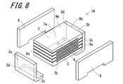
- FIG. 7 is a perspective view showing an example of a laminated ceramic electronic component according to another embodiment of the present disclosure
- FIG. 8 is an exploded perspective view showing the laminated ceramic electronic component of FIG.
- a laminated ceramic capacitor 1A of this embodiment differs from the laminated ceramic capacitor 1 of the above-described embodiment in the configurations of the first external electrode 3a, the second external electrode 3b, and the protective layer 6, and the rest is the same. Since it is a structure, the same reference numerals as those of the multilayer ceramic capacitor 1 are assigned to the same structures, and detailed description thereof will be omitted.
- the first external electrode 3a extends from the first end surface 8a to one of the principal surfaces 7a and 7b (the second surface 7b in FIG. 8).
- the second external electrode 3b extends from the second end surface 8b to one of the main surfaces 7a and 7b (the second surface 7b in FIG. 8).
- the protective layer 6 covers the first side surface 9a and the second side surface 9b of the base component 2, and the external electrode side surfaces 3c and 3d of the first external electrode 3a and the second external electrode 3b.
- the protective layer 6 has an inverted U shape, for example, as shown in FIGS. In FIG. 7, the boundary between the base component 2 and the protective layer 6 is indicated by a chain double-dashed line for convenience of explanation, but the actual boundary does not appear clearly.
- the multilayer ceramic capacitor 1A can narrow the space s between the adjacent multilayer ceramic capacitors 1A, similarly to the multilayer ceramic capacitor 1 of the above embodiment.
- the entire multilayer ceramic capacitor 1A is It is possible to increase the thickness of the base component 2 in the stacking direction without increasing the thickness. As a result, it is possible to increase the acquired capacitance of the multilayer ceramic capacitor 1A while reducing the increase in the size of the multilayer ceramic capacitor 1A.
- FIG. 9 is a perspective view showing an example of a laminated ceramic electronic component according to still another embodiment of the present disclosure
- FIG. 10 is a cross-sectional view taken along line DD in FIG.
- the multilayer ceramic capacitor 1B of the present embodiment differs from the multilayer ceramic capacitor 1 and the multilayer ceramic capacitor 1A of the above-described embodiments in the configuration of the protective layer 6, and the rest of the configuration is the same.
- the same reference numerals as those of the laminated ceramic capacitor 1 and the laminated ceramic capacitor 1A are assigned to the configuration, and detailed description thereof will be omitted.
- the main surfaces 7a and 7b of the base component 2 from the external electrode side surface 3d wraps around the surfaces of the first external electrode 3a and the second external electrode 3b that are continuous with the external electrode side surface 3c and the external electrode side surface 3d.
- the protective layer 6 covers the base component 2 and the external electrode base layer 15 from the sides (left and right direction in FIG. 10), and also covers the main surfaces 7a and 7b of the external electrode base layer 15. It wraps around the side face.
- the plating outer layer 16 is formed in a region where the protective layer 6 does not exist on the surface of the external electrode underlying layer 15 .
- the protective layer 6 extends from the side surfaces 9a and 9b of the base component 2 to the main surfaces 7a and 7b. Therefore, when a plurality of laminated ceramic capacitors 1B are mounted on a circuit board, the physical distance between the first external electrodes 3a and the second external electrodes 3b of the mutually adjacent laminated ceramic capacitors 1B can be increased. As a result, it is possible to reduce the risk of short-circuiting between adjacent multilayer ceramic capacitors 1B. As a result, the reliability of the circuit board on which the multilayer ceramic capacitors 1B are mounted at high density can be improved.
- the protective layer 6 may extend from the first side surface 9a and the second side surface 9b of the base component 2 to the first surface 7a and the second surface 7b and the first end surface 8a and the second end surface 8b. Therefore, it is possible to effectively reduce the risk of short-circuiting between adjacent laminated ceramic capacitors 1B, and further improve the reliability of the circuit board on which the laminated ceramic capacitors 1B are mounted at high density.
- the shape of the base component 2 changes in the step of green processing before firing, so for convenience of explanation, refer to the exploded perspective view shown in FIG.
- the element body part 2 on which the external electrode base layer 15 of the external electrode 3 is formed is called the second element body part
- the second element body part on which the protective layer 6 is formed is called the third element body part.
- ceramic mixed powder obtained by adding an additive to BaTiO 3 which is the material of the ceramic layer 4, is wet pulverized and mixed by a bead mill. make.
- a ceramic green sheet 10 is formed on the carrier film.
- the thickness of the ceramic green sheet 10 may be, for example, about 0.5 ⁇ m to 10 ⁇ m. As the ceramic green sheets 10 are thinner, the capacitance of the multilayer ceramic capacitor 1 can be increased.
- the molding of the ceramic green sheet 10 is not limited to the method using a die coater, and may be performed using a doctor blade coater, a gravure coater, or the like.
- a conductive paste 5a containing a metal material to be the internal electrode layers 5 is printed on the ceramic green sheet 10 formed as described above in a band-like pattern of a plurality of rows using a gravure printing method. do.
- the conductive paste 5a may contain metals such as Ni (nickel), Pd (palladium), Cu (copper), Ag (silver), or alloys thereof.
- the method for printing the conductive paste 5a is not limited to the gravure printing method, and may be a screen printing method or the like.
- the thickness of the internal electrode layers 5 may be about 1.5 ⁇ m or less.
- a predetermined number of ceramic green sheets 10 printed with an internal electrode layer pattern made of conductive paste 5a are stacked on a predetermined number of ceramic green sheets 10, and finally ceramic green sheets 10 are laminated.
- a predetermined number of sheets 10 are laminated.
- the ceramic green sheets 10 on which the internal electrode layer patterns are printed are stacked while being shifted by half of the widthwise dimension of the internal electrode layer patterns.
- lamination of the ceramic green sheets 10 is performed on a support sheet.
- an adhesive release sheet that can be adhered and peeled, such as a weak adhesive sheet or a foamed release sheet, can be used.
- the laminate of the ceramic green sheets 10 is pressed in the lamination direction using a hydrostatic press to produce a mother laminate 11 in which a plurality of ceramic green sheets 10 are integrated as shown in FIG. 13, for example. do.
- a virtual dividing line 30 is indicated by a two-dot chain line on the surface of the mother laminate 11 .
- Individual parts separated by virtual dividing lines 30 correspond to the base part 2 shown in FIG.
- the mother laminate 11 has a pair of principal surfaces, which correspond to the principal surfaces 7 a and 7 b of the base component 2 .
- the mother laminate 11 has a pair of end faces, which correspond to the end faces 8 a and 8 b of the base component 2 .
- the mother laminate 11 has a pair of side surfaces, which correspond to the side surfaces 9 a and 9 b of the base component 2 .
- the part of the intermediate in each step of the manufacturing method of the multilayer ceramic electronic component may be specified by using the name of the corresponding part of the multilayer ceramic electronic component 1 .
- a support sheet used when stacking the plurality of ceramic green sheets 10 is present on the lower surface of the mother laminate 11 .
- a press cutting machine is used to cut the mother laminate 11 at predetermined intervals to produce a plurality of first rod-shaped bodies 12 .
- the cutting of the mother laminate 11 to obtain the plurality of first rod-shaped bodies 12 may be referred to as the first cutting.
- the surfaces formed by the first cutting of the first rod-shaped body 12 are sometimes referred to as a first cut surface CP1 and a second cut surface CP2.
- the first cut surface CP1 and the second cut surface CP2 correspond to the first end surface 8a and the second end surface 8b of the base component 2, respectively, and the internal electrode layers 5 of one of the internal electrode layers 5 having different polarities is exposed.
- the cutting of the mother laminated body 11 is not limited to cutting using a press cutting machine, and may be cutting using a dicing saw device or the like.
- V-grooves 19 are formed.
- the V-groove 19 can be formed using, for example, a dicing saw.
- a V-groove 19 having a depth of about 10 ⁇ m from the second surface 7b is formed at the position cut by the first cutting. Note that the V-groove 19 may be formed before the first cutting.
- the V-groove 19 is for chamfering the edges that appear by the first cutting. By chamfering the edges, it is possible to form the external electrode base layer 15 having a thickness equal to or greater than a predetermined value.
- the first rod-shaped body 12 has, for example, a shape as shown in FIG. 3 when viewed from the longitudinal direction (direction perpendicular to the end surface 8).
- the chamfering distance b of the first rod-shaped body 12 may be 4 ⁇ m or more.
- the chamfering distance b is defined as a first bar-like distance from the intersection line where the extended surfaces of the main surfaces 7a and 7b and the extended surfaces of the end surfaces 8a and 8b (the first cut surface CP1 and the second cut surface CP2) intersect.
- the thickness of the external electrode base layer 15 tends to be thin at the corners connecting the main surfaces 7a, 7b and the end surfaces 8a, 8b. As a result, the external electrode base layer 15 becomes discontinuous, and the electrical reliability of the multilayer ceramic capacitor may deteriorate.
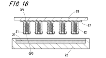
- the plurality of first rods 12 are arranged such that one of the first cut plane CP1 and the second cut plane CP2 (the first cut plane CP1 in FIG. 15) is one virtual plane. be positioned within P.
- the plurality of first rod-shaped bodies 12 are fixed on the support sheet 17 .
- the virtual plane P may be the surface of the support sheet 17 .
- the support sheet 17 is for temporarily fixing the first rod-shaped body 12 . In a later step, it is necessary to remove the element parts 2 obtained by dividing the rod-shaped body into individual pieces from the support sheet 17. Therefore, the support sheet 17 is made of a high-temperature foaming adhesive sheet, a temperature-sensitive peelable adhesive sheet, or the like, which can be peeled off. It may be an adhesive sheet.
- the external electrode base layer 15 and the external electrode base layer 15 are formed on the other of the first cut surface CP1 and the second cut surface CP2 of the first rod 12 (the second cut surface CP2 in FIG. 16). Then, the external electrode paste 21 is applied.
- the second cut surface CP2 of the first rod-shaped body 12 is immersed in the external electrode paste 21 to a predetermined depth, pulled out, and then dried. Subsequently, the support sheet 17 is transferred, and the external electrode paste 21 is applied to the first cut surface CP1 of the first rod-shaped body 12 in the same process.
- the external electrode paste 21 is composed of an inorganic material, a binder and a solvent.
- the inorganic material includes a ceramic material containing barium titanate as the main component, which is the same as or similar to the ceramic layer 4 of the base component 2, and a conductive metal material containing nickel or a nickel alloy as the main component, which is the same as or similar to the internal electrode layer 5. consists of As a result, the sintering behaviors of the external electrode base layer 15 and the base component 2 at high temperature can be made close to each other in the subsequent firing process.
- the ceramic material of the external electrode base layer 15 and the dielectric ceramic layer 4 of the base component 2 are sintered and bonded, and the conductive metal material of the external electrode base layer 15 and the internal electrode layer 5 of the base component 2 are bonded together. It is possible to strengthen the connection between the external electrode base layer 15 and the base component 2 by sintering.
- the first rod-shaped body 12 coated with the external electrode paste 21 may be referred to as a second rod-shaped body 24 in order to distinguish it from the first rod-shaped body 12 .
- FIG. 17 shows a plurality of second rod-shaped bodies 24 aligned.
- a press-cutting machine having a press-cutting blade 14 is used to perform a second cut on the assembly of the plurality of second rod-shaped bodies 24 .
- one of the first cut surface CP1 and the second cut surface CP2 (the first cut surface CP1 in FIG. 18) formed by first cutting the plurality of second rod-shaped bodies 24 is one virtual cut surface CP1. It may be arranged so as to be positioned within the plane P.
- the imaginary plane P may be the surface of a cutting plate (not shown).
- the assembly may be a collection of a plurality of second rod-shaped bodies 24 such that the longer side of the sides excluding the sides extending in the longitudinal direction extends in the vertical direction.
- a pair of dummy members 37 are arranged on both sides of the aggregate of the plurality of second rod-shaped bodies 24 to sandwich the aggregate from both sides. You may fix the several 2nd rod-shaped body 24 by.
- the pair of dummy members 37 may be cut together with the plurality of second rod-shaped bodies 24 in the second cutting.
- a plurality of second rod-shaped bodies 24 are arranged so that the main surfaces 7a and 7b of the second rod-shaped bodies 24 adjacent to each other are opposed to each other, the main surfaces 7a and 7b are arranged with respect to the surface of the cutting plate. Since it is vertical, it is possible to increase the number of second rod-shaped bodies 24 that can be placed on the cutting plate, and to improve production efficiency.
- the main surfaces 7a and 7b of the plurality of second rod-shaped bodies 24 are brought into contact with each other, the main surfaces 7a and 7b are substantially in contact with the external electrodes 3. Since it is a narrow region in (external electrode base layer 15), it is possible to reduce the possibility that the base body parts 2 will come into contact with each other and join together when performing the second cutting.
- the dummy members 37 to be cut together with the second rod-shaped body 24 are arranged on both sides, it is possible to reduce the change in the position or posture of the second rod-shaped body 24 during the second cutting. .
- the second rod-like body 24 becomes a chip-like component on which the external electrode base layer 15 is formed. It is sometimes called body part 13 .
- the plurality of second element parts 13 are cut by one of the third cut plane CP3 and the fourth cut plane CP4 formed by the second cutting (the third cut plane in FIG. 19).
- the cutting plane CP3) is arranged so as to be positioned within one virtual plane P.
- the virtual plane P may be the surface of the support sheet 17
- the plurality of second element body parts 13 may be fixed on the support sheet 17 .
- the support sheet 17 is for temporarily fixing the second element body part 13, and since the second element body part 13 is removed in a later process, the support sheet 17 may be a high-temperature foaming adhesive sheet or a temperature-sensitive peeling sheet. Use a removable adhesive sheet such as a mold adhesive sheet.
- a protective layer 6 containing a ceramic material is formed on the side surface of the second element body part 13 .
- the support sheet 17 is transferred to the surface coated with the ceramic paste 20, the same process is repeated, and the ceramic paste 20 is dip-coated on the opposite side surface (third cut surface CP3), and then dried.
- the ceramic paste 20 after drying is the protective layer 6 and extends from the side surfaces 9a and 9b of the second element body part 13 and the external electrode side surfaces 3c and 3d to adjacent surfaces adjacent thereto.
- the thickness of the protective layer 6 after drying may be 5 ⁇ m to 30 ⁇ m.
- the amount of wraparound of the protective layer 6 to the adjacent surface is increased, the surface areas of the first external electrode 3a and the second external electrode 3b are reduced, which may make it difficult to mount them well on the circuit board.
- the amount of wraparound to the adjacent surface of layer 6 may range from 0 ⁇ m to 50 ⁇ m.
- the ceramic paste 20 may have the same or similar components as the main component of the ceramic layer 4 and the main component of the protective layer 6 .
- a ceramic slurry having the same or similar components as the main components of the ceramic layer 4 and the protective layer 6 may be used. Further, when forming the protective layer 6, for example, as shown in FIG. As a result, handling of the plurality of second element parts 13 can be improved.
- FIG. 21 shows the third element body part 27 on which the protective layer 6 obtained in the process of FIG. 20 is formed. Since the third element body part 27 is uniformly shrunk and sintered in the subsequent firing process, FIG. 21 shows the third element body part 27 before firing and the third body part 27 after firing. is shown.
- the third element body part 27 is barrel-polished and chamfered. Chamfering is to round the corners of the third element body part 27 and remove burrs.
- the fired third element body part 27 and the polishing material are placed in a pot containing water and rotated to perform polishing.
- the plating outer layer 16 is formed on the surface of the external electrode base layer 15 .
- a plurality of plating outer layers 16 are formed.
- a Ni plating layer is formed on the surface of the external electrode base layer 15 in an electrolytic plating tank. Furthermore, by forming a Sn plating layer on the surface of the Ni plating layer, the multilayer ceramic capacitor 1 shown in FIG. 9 can be manufactured.
- the manufacturing method of the multilayer ceramic electronic component of this embodiment is a manufacturing method of manufacturing the multilayer ceramic capacitor 1 shown in FIG.
- the manufacturing method is the same as the manufacturing method of the multilayer ceramic electronic component of the above-described embodiment until obtaining.
- a plurality of second rod-shaped bodies 24 shown in FIG. and a thermoplastic resin sheet 34 is arranged thereabove. Further, flat plates 28 are arranged above and below the plurality of second rod-shaped bodies 24, the resin sheet 34, and the frame-shaped or column-shaped spacers 36 surrounding the plurality of second rod-shaped bodies 24, which are arranged on the support sheet 17, respectively. .
- the height of the spacers 36 is set higher than the height of the plurality of second rod-shaped bodies 24 by about 0 to 0.1 mm.
- the height of the spacers 36 may depend on the dimensions of the laminated ceramic capacitor to be manufactured, but by setting the height to include the variations in the heights of the plurality of second rod-shaped bodies 24, the spacers 36 can be used in later steps. The amount of resin can be reduced.
- the resin sheet 34 is heated while being pressed in the direction indicated by the arrow F.
- the resin sheet 34 is melted by heating and flows into the gaps between the second rod-shaped bodies 24 adjacent to each other.
- the frame-shaped or column-shaped spacer 36 secures the interval between the flat plates 28 arranged above and below the plurality of second rod-shaped bodies 24 and reduces the flow of the molten resin sheet 34.
- thermoplastic resin 33 (also referred to as a block) 23 is produced.
- the assembly 23 is cut at predetermined intervals in a direction orthogonal to the longitudinal direction of the second rod-shaped body 24 (second cutting), A third rod-shaped body 25 having a third cut surface CP3 and a fourth cut surface CP4 is produced.
- the cutting of the assembly 23 is not limited to cutting using the press cutting blade 14, but may be cutting using a dicing saw device or the like.
- the third rod-shaped body 25 is formed by integrating chip-like element parts on which the external electrode base layer 15 is formed in a row. Therefore, it is possible to improve the handleability in the subsequent steps, and thus the productivity of the laminated ceramic capacitor 1 can be improved.
- each of the plurality of third rod-shaped bodies 25 is rotated 90 degrees around the longitudinal axis, and one of the third cut surface CP3 and the fourth cut surface CP4 where the internal electrode layer 5 is exposed is cut. (The fourth cut plane CP4 in FIG. 24) faces upward.
- a plurality of third rods 25 are assembled with one of the third cut plane CP3 and the fourth cut plane CP4 (fourth cut plane CP4 in FIG. 24) facing upward.
- ceramic green sheets 10 that serve as protective layers 6 are arranged on the upper and lower surfaces of the assembly of the plurality of third rod-shaped bodies 25 .
- the ceramic green sheets 10 may not be arranged on the upper surface and the lower surface of the assembly at the same time, but may be arranged on each surface.
- FIG. 25 shows the assembly after isostatic pressing.
- the third rod-shaped body 25 is a fourth rod-shaped body 26 to which the ceramic green sheet 10 that forms the protective layer 6 is applied.
- the protective layer 6 brings the ceramic green sheet 10 into contact with the third cut surface CP3 and the fourth cut surface CP4, and places the portion of the ceramic green sheet 10 in contact with the third cut surface CP3 into the third cut surface CP3.
- a plurality of third rod-shaped bodies 25 can be formed by transferring and transferring the portions in contact with the fourth cut plane CP4 to the fourth cut plane CP4.
- the ceramic green sheet 10 serving as the protective layer 6 may be a single-layer ceramic green sheet or a multi-layer ceramic green sheet. The multiple layers of ceramic green sheets may have components different from each other.
- the fourth rod-shaped body 26 is degreased and fired.
- a plurality of fourth rod-shaped bodies 26 are arranged on a zirconia plate, the plurality of fourth rod-shaped bodies 26 arranged on the plate are placed in a degreasing furnace to remove the solvent and binder, and then placed in a high-temperature firing furnace.
- Bake The degreasing treatment is performed in the atmosphere from room temperature to about 300°C to remove solvents and plasticizers, and then up to 800°C in a nitrogen atmosphere to thermally decompose and burn resins such as binders and fixing resins. remove by In the firing process, for example, firing may be performed at a temperature of 1100 to 1250° C. in a mixed atmosphere of hydrogen.
- the thermoplastic resin 33 surrounding the third rod-shaped body 25 is decomposed and burned away, and the space between the third element parts 27 adjacent to each other is eliminated. is the void 31 .
- the third element body parts 27 shrink during the sintering process, and the gaps between the third element body parts 27 widen. The site is cracked and a parting line 32 is formed.
- the plurality of third element body parts 27 having the external electrodes 3 and the protective layers 6 formed thereon are substantially divided into individual pieces.
- the third element body part 27 is barrel-polished and chamfered.
- the chamfering process is the same as in the above embodiment, and the sintering residue of the ceramic green sheets generated between the third element parts 27 is removed by barrel polishing.
- the steps following the chamfering step are the same as those in the above embodiment, so detailed descriptions thereof are omitted.
- the manufacturing method of the multilayer ceramic electronic component of the present embodiment is the same as the manufacturing method of the multilayer ceramic electronic component of the above-described embodiment until the mother laminate 11 shown in FIG. 13 is obtained. Since the supporting sheet is omitted in FIG. 13, FIG. As the support sheet 18, a high-temperature foaming pressure-sensitive adhesive sheet or a temperature-sensitive peel-type pressure-sensitive adhesive sheet that loses its adhesive force at high temperatures, like the support sheet 17, can be used.
- a press cutting machine is used to cut the mother laminate 11 at predetermined intervals to produce a plurality of first rod-shaped bodies 12 .
- the support sheet 18 is cut together with the mother laminate 11 .
- a first cut surface CP1 and a second cut surface CP2 formed by the first cutting correspond to the first end surface 8a and the second end surface 8b of the base component 2 shown in FIG. 8, respectively.
- the plurality of internal electrode layers 5 are exposed on either one of the first cut surface CP1 and the second cut surface CP2 according to polarity.
- the cutting of the mother laminated body 11 is not limited to cutting using a press cutting machine, and may be cutting using a dicing saw device or the like.
- V-grooves 19 having a depth of about 10 ⁇ m from the main surfaces 7a and 7b are formed at the positions cut by the first cutting.
- the V-groove 19 can be formed using, for example, a dicing saw.
- the V-groove 19 is for chamfering the edges that appear by the first cutting. By chamfering the edges, it is possible to form the external electrode base layer 15 having a thickness equal to or greater than a predetermined value. Note that the V-groove 19 may be formed before the first cutting.
- the plurality of first rods 12 are arranged so that one of the first cut surface CP1 and the second cut surface CP2 (the second cut surface CP2 in FIG. 29) faces upward. , are placed and fixed on the support sheet 17 .
- the support sheet 17 is for temporarily fixing the first rod-shaped body 12 .
- a peelable adhesive sheet such as a high-temperature foaming adhesive sheet or a temperature-sensitive peelable adhesive sheet can be used.
- an external An external electrode paste 21 to be the electrode base layer 15 is applied.
- the second cut surface CP2 of the first rod-shaped body 12 with the support sheet 18 is immersed in the external electrode paste 21 accommodated in the pool 22 to a predetermined depth, pulled up, and then dried.
- the support sheet 18 is transferred, and the external electrode paste is applied to the other of the first cut surface CP1 and the second cut surface CP2 of the first rod 12 (the first cut surface CP1 in FIG. 30) in the same process. 21 is applied.
- the external electrode base layer 15 for example, as shown in FIG. Thereby, the handleability of the plurality of first rod-shaped bodies 12 can be improved.
- the external electrode paste 21 is composed of an inorganic material, a binder and a solvent.
- the inorganic material is composed of a ceramic dielectric material containing barium titanate as the main component, which is the same as the element body, and a conductive metal material containing nickel or a nickel alloy as the main component, which is the same as the internal electrode layers.
- the external electrode base layer 15 is also formed on the support sheet 18 located on the first surface 7a of the second rod-shaped body 24 (the first rod-shaped body 12 coated with the external electrode paste 21), as shown in FIG. 31, for example.
- a high-temperature foamed adhesive sheet or a temperature-sensitive peelable adhesive sheet that loses its adhesive force at high temperatures is used as the support sheet 18. Therefore, when the external electrode paste 21 is dried, the support sheet 18 does not adhere to the surface shown in FIG. It is separated from the second rod-shaped body 24 along the separation line 39 shown in FIG.
- FIG. 32 shows a plurality of second rod-shaped bodies 24 from which the support sheet 18 has been peeled off.
- a laminated ceramic electronic component of the present disclosure includes a substantially rectangular parallelepiped element component, a first external electrode, a second external electrode, and a protective layer.
- the element body component is formed by alternately laminating a plurality of ceramic layers and a plurality of internal electrode layers having different polarities. It has a face and a second face, a first end face and a second end face facing each other, and a first side face and a second side face facing each other.
- the plurality of internal electrode layers are exposed on the first side surface and the second side surface, and are exposed on either one of the first end surface and the second end surface according to polarity.
- the first external electrode is connected to the internal electrode layer exposed on the first end surface
- the second external electrode is connected to the internal electrode layer exposed on the second end surface.
- Each of the first external electrode and the second external electrode extends over at least one of the first surface and the second surface and is flush with the first side surface and the second side surface, respectively. It has one external electrode side surface and a second external electrode side surface.
- the protective layer contains a ceramic material and covers the first and second side surfaces and the first and second external electrode side surfaces of the first and second external electrodes.
- a mother laminated body in which a plurality of ceramic green sheets and a plurality of internal electrode layers are alternately laminated is cut at predetermined intervals, and the first surface and the second surface are cut.
- a first rod-shaped body having a surface, a first cut surface and a second cut surface is produced, and edges between the first surface and the second surface and the first cut surface and the second cut surface are formed.
- a body is prepared, and the second rod-shaped body is cut at predetermined intervals in a direction perpendicular to the longitudinal direction of the second rod-shaped body, and the plurality of internal electrode layers are exposed on the third cut surface and the fourth cut surface. and forming a protective layer containing a ceramic material on each of the third cut surface and the fourth cut surface.
- the multilayer ceramic electronic component of the present disclosure When the multilayer ceramic electronic component of the present disclosure is mounted on a circuit board, it is possible to reduce the possibility that the external electrodes of mutually adjacent multilayer ceramic electronic components are short-circuited. becomes possible.
- the above-described laminated ceramic electronic component can be manufactured with reduced manufacturing burden and with good productivity.
- the protective layer may be provided by attaching a ceramic green sheet to the rod-shaped body or element part, or by dip-coating the rod-shaped body or element part with a ceramic slurry.
- the material of the protective layer and the material of the base component are substantially the same material or a similar material. , the material of the protective layer and the material of the base component may be different.
Landscapes
- Engineering & Computer Science (AREA)
- Power Engineering (AREA)
- Microelectronics & Electronic Packaging (AREA)
- Manufacturing & Machinery (AREA)
- Ceramic Engineering (AREA)
- Chemical & Material Sciences (AREA)
- Physics & Mathematics (AREA)
- Electromagnetism (AREA)
- Inorganic Chemistry (AREA)
- Fixed Capacitors And Capacitor Manufacturing Machines (AREA)
- Ceramic Capacitors (AREA)
Priority Applications (3)
| Application Number | Priority Date | Filing Date | Title |
|---|---|---|---|
| US18/567,481 US12437928B2 (en) | 2021-06-23 | 2022-06-07 | Multilayer ceramic electronic component and method for manufacturing multilayer ceramic electronic component |
| JP2023529807A JP7602637B2 (ja) | 2021-06-23 | 2022-06-07 | 積層セラミック電子部品およびその製造方法 |
| CN202280042572.9A CN117642831A (zh) | 2021-06-23 | 2022-06-07 | 层叠陶瓷电子部件及其制造方法 |
Applications Claiming Priority (2)
| Application Number | Priority Date | Filing Date | Title |
|---|---|---|---|
| JP2021-104419 | 2021-06-23 | ||
| JP2021104419 | 2021-06-23 |
Publications (1)
| Publication Number | Publication Date |
|---|---|
| WO2022270299A1 true WO2022270299A1 (ja) | 2022-12-29 |
Family
ID=84544552
Family Applications (1)
| Application Number | Title | Priority Date | Filing Date |
|---|---|---|---|
| PCT/JP2022/023004 Ceased WO2022270299A1 (ja) | 2021-06-23 | 2022-06-07 | 積層セラミック電子部品およびその製造方法 |
Country Status (4)
| Country | Link |
|---|---|
| US (1) | US12437928B2 (https=) |
| JP (1) | JP7602637B2 (https=) |
| CN (1) | CN117642831A (https=) |
| WO (1) | WO2022270299A1 (https=) |
Families Citing this family (1)
| Publication number | Priority date | Publication date | Assignee | Title |
|---|---|---|---|---|
| JP7602637B2 (ja) * | 2021-06-23 | 2024-12-18 | 京セラ株式会社 | 積層セラミック電子部品およびその製造方法 |
Citations (4)
| Publication number | Priority date | Publication date | Assignee | Title |
|---|---|---|---|---|
| JPS6086882A (ja) * | 1983-10-18 | 1985-05-16 | Nec Corp | 電歪効果素子の製造方法 |
| JPH11340081A (ja) * | 1998-05-21 | 1999-12-10 | Murata Mfg Co Ltd | 積層セラミック電子部品及びその製造方法 |
| JP2014187216A (ja) * | 2013-03-23 | 2014-10-02 | Kyocera Corp | 積層セラミックコンデンサの製造方法 |
| JP2021015950A (ja) * | 2019-07-16 | 2021-02-12 | 株式会社村田製作所 | 積層セラミックコンデンサ |
Family Cites Families (9)
| Publication number | Priority date | Publication date | Assignee | Title |
|---|---|---|---|---|
| JP2013058558A (ja) * | 2011-09-07 | 2013-03-28 | Tdk Corp | 電子部品 |
| KR101376921B1 (ko) * | 2012-12-11 | 2014-03-20 | 삼성전기주식회사 | 적층 세라믹 커패시터 및 그 제조방법 |
| KR101525662B1 (ko) * | 2013-04-26 | 2015-06-03 | 삼성전기주식회사 | 적층 세라믹 전자부품 및 적층 세라믹 전자부품 실장 기판 |
| KR102057913B1 (ko) * | 2013-07-04 | 2019-12-20 | 삼성전기주식회사 | 적층 세라믹 전자 부품 및 그 제조 방법 |
| KR101884392B1 (ko) | 2015-03-30 | 2018-08-02 | 다이요 유덴 가부시키가이샤 | 적층 세라믹 콘덴서 |
| JP6436921B2 (ja) | 2015-03-30 | 2018-12-12 | 太陽誘電株式会社 | 積層セラミックコンデンサ |
| JP7358692B2 (ja) * | 2018-06-15 | 2023-10-11 | サムソン エレクトロ-メカニックス カンパニーリミテッド. | キャパシタ部品及びキャパシタ部品の製造方法 |
| JP7401320B2 (ja) * | 2020-01-24 | 2023-12-19 | 株式会社村田製作所 | 積層セラミック電子部品 |
| JP7602637B2 (ja) * | 2021-06-23 | 2024-12-18 | 京セラ株式会社 | 積層セラミック電子部品およびその製造方法 |
-
2022
- 2022-06-07 JP JP2023529807A patent/JP7602637B2/ja active Active
- 2022-06-07 US US18/567,481 patent/US12437928B2/en active Active
- 2022-06-07 CN CN202280042572.9A patent/CN117642831A/zh active Pending
- 2022-06-07 WO PCT/JP2022/023004 patent/WO2022270299A1/ja not_active Ceased
Patent Citations (4)
| Publication number | Priority date | Publication date | Assignee | Title |
|---|---|---|---|---|
| JPS6086882A (ja) * | 1983-10-18 | 1985-05-16 | Nec Corp | 電歪効果素子の製造方法 |
| JPH11340081A (ja) * | 1998-05-21 | 1999-12-10 | Murata Mfg Co Ltd | 積層セラミック電子部品及びその製造方法 |
| JP2014187216A (ja) * | 2013-03-23 | 2014-10-02 | Kyocera Corp | 積層セラミックコンデンサの製造方法 |
| JP2021015950A (ja) * | 2019-07-16 | 2021-02-12 | 株式会社村田製作所 | 積層セラミックコンデンサ |
Also Published As
| Publication number | Publication date |
|---|---|
| US12437928B2 (en) | 2025-10-07 |
| CN117642831A (zh) | 2024-03-01 |
| US20240274359A1 (en) | 2024-08-15 |
| JP7602637B2 (ja) | 2024-12-18 |
| JPWO2022270299A1 (https=) | 2022-12-29 |
Similar Documents
| Publication | Publication Date | Title |
|---|---|---|
| JP5293506B2 (ja) | セラミック電子部品及びセラミック電子部品の製造方法 | |
| JP5278149B2 (ja) | 回路基板及び回路モジュール | |
| CN107926122B (zh) | 多层陶瓷基片的制造方法 | |
| JP7696860B2 (ja) | 積層セラミック電子部品およびその製造方法 | |
| JP2010021386A (ja) | セラミック部品の製造方法 | |
| JP7602637B2 (ja) | 積層セラミック電子部品およびその製造方法 | |
| JP4284782B2 (ja) | 多層セラミック基板およびその製造方法 | |
| JP2000340448A (ja) | 積層セラミックコンデンサ | |
| JP5314370B2 (ja) | セラミック部品の製造方法 | |
| TWI869882B (zh) | 積層陶瓷電子零件 | |
| TWI840898B (zh) | 積層陶瓷電子零件及其製造方法 | |
| CN117393322A (zh) | 一种多层陶瓷电容器及其制备方法 | |
| JP2005268672A (ja) | 基板 | |
| JPWO2006040941A1 (ja) | 積層セラミック部品とその製造方法 | |
| JP4697600B2 (ja) | 複合配線基板の製造方法 | |
| JP4089356B2 (ja) | 多層セラミック基板の製造方法 | |
| JP4038616B2 (ja) | 多層セラミック基板の製造方法 | |
| KR100956212B1 (ko) | 다층 세라믹 기판의 제조 방법 | |
| JP2005286303A (ja) | 積層セラミック基板およびその製造方法 | |
| JP2004128134A (ja) | セラミック積層基板及びその製造方法 | |
| JPH11340082A (ja) | 積層チップ部品とその製造方法 | |
| TWI869872B (zh) | 積層陶瓷電子零件及積層陶瓷電子零件之製造方法 | |
| JP2006041319A (ja) | 表面実装型多連コンデンサ及びその実装構造 | |
| US20090230596A1 (en) | Method of manufacturing multi-layered ceramic substrate | |
| JP5573407B2 (ja) | 金属ベース基板 |
Legal Events
| Date | Code | Title | Description |
|---|---|---|---|
| 121 | Ep: the epo has been informed by wipo that ep was designated in this application |
Ref document number: 22828216 Country of ref document: EP Kind code of ref document: A1 |
|
| WWE | Wipo information: entry into national phase |
Ref document number: 18567481 Country of ref document: US |
|
| WWE | Wipo information: entry into national phase |
Ref document number: 2023529807 Country of ref document: JP |
|
| WWE | Wipo information: entry into national phase |
Ref document number: 202280042572.9 Country of ref document: CN |
|
| NENP | Non-entry into the national phase |
Ref country code: DE |
|
| 122 | Ep: pct application non-entry in european phase |
Ref document number: 22828216 Country of ref document: EP Kind code of ref document: A1 |
|
| WWG | Wipo information: grant in national office |
Ref document number: 18567481 Country of ref document: US |