WO2022264844A1 - 半導体装置 - Google Patents
半導体装置 Download PDFInfo
- Publication number
- WO2022264844A1 WO2022264844A1 PCT/JP2022/022702 JP2022022702W WO2022264844A1 WO 2022264844 A1 WO2022264844 A1 WO 2022264844A1 JP 2022022702 W JP2022022702 W JP 2022022702W WO 2022264844 A1 WO2022264844 A1 WO 2022264844A1
- Authority
- WO
- WIPO (PCT)
- Prior art keywords
- semiconductor elements
- semiconductor
- electrode
- semiconductor device
- elements
- Prior art date
- Legal status (The legal status is an assumption and is not a legal conclusion. Google has not performed a legal analysis and makes no representation as to the accuracy of the status listed.)
- Ceased
Links
Images





Classifications
-
- H—ELECTRICITY
- H10—SEMICONDUCTOR DEVICES; ELECTRIC SOLID-STATE DEVICES NOT OTHERWISE PROVIDED FOR
- H10W—GENERIC PACKAGES, INTERCONNECTIONS, CONNECTORS OR OTHER CONSTRUCTIONAL DETAILS OF DEVICES COVERED BY CLASS H10
- H10W70/00—Package substrates; Interposers; Redistribution layers [RDL]
- H10W70/60—Insulating or insulated package substrates; Interposers; Redistribution layers
- H10W70/62—Insulating or insulated package substrates; Interposers; Redistribution layers characterised by their interconnections
- H10W70/65—Shapes or dispositions of interconnections
-
- H—ELECTRICITY
- H02—GENERATION; CONVERSION OR DISTRIBUTION OF ELECTRIC POWER
- H02M—APPARATUS FOR CONVERSION BETWEEN AC AND AC, BETWEEN AC AND DC, OR BETWEEN DC AND DC, AND FOR USE WITH MAINS OR SIMILAR POWER SUPPLY SYSTEMS; CONVERSION OF DC OR AC INPUT POWER INTO SURGE OUTPUT POWER; CONTROL OR REGULATION THEREOF
- H02M1/00—Details of apparatus for conversion
- H02M1/08—Circuits specially adapted for the generation of control voltages for semiconductor devices incorporated in static converters
-
- H—ELECTRICITY
- H10—SEMICONDUCTOR DEVICES; ELECTRIC SOLID-STATE DEVICES NOT OTHERWISE PROVIDED FOR
- H10W—GENERIC PACKAGES, INTERCONNECTIONS, CONNECTORS OR OTHER CONSTRUCTIONAL DETAILS OF DEVICES COVERED BY CLASS H10
- H10W70/00—Package substrates; Interposers; Redistribution layers [RDL]
- H10W70/60—Insulating or insulated package substrates; Interposers; Redistribution layers
- H10W70/611—Insulating or insulated package substrates; Interposers; Redistribution layers for connecting multiple chips together
-
- H—ELECTRICITY
- H10—SEMICONDUCTOR DEVICES; ELECTRIC SOLID-STATE DEVICES NOT OTHERWISE PROVIDED FOR
- H10W—GENERIC PACKAGES, INTERCONNECTIONS, CONNECTORS OR OTHER CONSTRUCTIONAL DETAILS OF DEVICES COVERED BY CLASS H10
- H10W70/00—Package substrates; Interposers; Redistribution layers [RDL]
- H10W70/60—Insulating or insulated package substrates; Interposers; Redistribution layers
- H10W70/62—Insulating or insulated package substrates; Interposers; Redistribution layers characterised by their interconnections
- H10W70/65—Shapes or dispositions of interconnections
- H10W70/658—Shapes or dispositions of interconnections for devices provided for in groups H10D8/00 - H10D48/00
-
- H—ELECTRICITY
- H10—SEMICONDUCTOR DEVICES; ELECTRIC SOLID-STATE DEVICES NOT OTHERWISE PROVIDED FOR
- H10W—GENERIC PACKAGES, INTERCONNECTIONS, CONNECTORS OR OTHER CONSTRUCTIONAL DETAILS OF DEVICES COVERED BY CLASS H10
- H10W72/00—Interconnections or connectors in packages
- H10W72/50—Bond wires
-
- H—ELECTRICITY
- H10—SEMICONDUCTOR DEVICES; ELECTRIC SOLID-STATE DEVICES NOT OTHERWISE PROVIDED FOR
- H10W—GENERIC PACKAGES, INTERCONNECTIONS, CONNECTORS OR OTHER CONSTRUCTIONAL DETAILS OF DEVICES COVERED BY CLASS H10
- H10W90/00—Package configurations
-
- H—ELECTRICITY
- H10—SEMICONDUCTOR DEVICES; ELECTRIC SOLID-STATE DEVICES NOT OTHERWISE PROVIDED FOR
- H10W—GENERIC PACKAGES, INTERCONNECTIONS, CONNECTORS OR OTHER CONSTRUCTIONAL DETAILS OF DEVICES COVERED BY CLASS H10
- H10W90/00—Package configurations
- H10W90/701—Package configurations characterised by the relative positions of pads or connectors relative to package parts
-
- H—ELECTRICITY
- H10—SEMICONDUCTOR DEVICES; ELECTRIC SOLID-STATE DEVICES NOT OTHERWISE PROVIDED FOR
- H10W—GENERIC PACKAGES, INTERCONNECTIONS, CONNECTORS OR OTHER CONSTRUCTIONAL DETAILS OF DEVICES COVERED BY CLASS H10
- H10W70/00—Package substrates; Interposers; Redistribution layers [RDL]
- H10W70/60—Insulating or insulated package substrates; Interposers; Redistribution layers
- H10W70/67—Insulating or insulated package substrates; Interposers; Redistribution layers characterised by their insulating layers or insulating parts
- H10W70/68—Shapes or dispositions thereof
- H10W70/6875—Shapes or dispositions thereof being on a metallic substrate, e.g. insulated metal substrates [IMS]
-
- H—ELECTRICITY
- H10—SEMICONDUCTOR DEVICES; ELECTRIC SOLID-STATE DEVICES NOT OTHERWISE PROVIDED FOR
- H10W—GENERIC PACKAGES, INTERCONNECTIONS, CONNECTORS OR OTHER CONSTRUCTIONAL DETAILS OF DEVICES COVERED BY CLASS H10
- H10W90/00—Package configurations
- H10W90/701—Package configurations characterised by the relative positions of pads or connectors relative to package parts
- H10W90/751—Package configurations characterised by the relative positions of pads or connectors relative to package parts of bond wires
- H10W90/754—Package configurations characterised by the relative positions of pads or connectors relative to package parts of bond wires between a chip and a stacked insulating package substrate, interposer or RDL
Definitions
- the present disclosure relates to semiconductor devices.
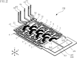
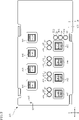
- the plurality of first semiconductor elements 1 includes a pair of first outer elements 1A and one or more first inner elements 1B.
- the plurality of first semiconductor elements 1 includes two first inner elements 1B.
- the pair of first outer elements 1A are elements positioned at both ends of the plurality of first semiconductor elements 1 in the first direction x.
- the first inner element 1B is an element positioned between the pair of first outer elements 1A in the first direction x among the plurality of first semiconductor elements 1 .
- the second frequency band includes, for example, resonance frequencies of a resonance circuit formed including parasitic inductance of the second conductive member.
- This resonant circuit further includes the parasitic capacitance (drain-gate capacitance) of each second semiconductor element 2 in the semiconductor device A1.
- Each of the pair of conductive plates 41 and 42 is made of a conductive material, such as copper or copper alloy. Different from this configuration, each of the conductive plates 41 and 42 may be a laminate in which a layer made of copper and a layer made of molybdenum are alternately laminated in the thickness direction z. In this case, both surface layers in the thickness direction z of each of the conductive plates 41 and 42 are layers made of copper.
- Each of the conductive plates 41 and 42 has, for example, a rectangular shape in plan view, as shown in FIG.
- the conductive plate 42 is mounted with a plurality of second semiconductor elements 2 and supports the plurality of second semiconductor elements 2, as shown in FIGS.
- the conductive plate 42 is electrically connected to the fourth electrode 21 (drain) of each second semiconductor element 2 .
- the fourth electrodes 21 of the plurality of second semiconductor elements 2 are electrically connected to each other via the conductive plate 42 .
- Conductive plate 42 has, for example, a rectangular parallelepiped shape.
- the dimension along the thickness direction z of the conductive plate 42 is larger than the dimension along the thickness direction z of the insulating substrate 50 .
- the conductive plate 42 is an example of a "second mounting portion".
- Each of the plurality of through holes 503 penetrates the insulating substrate 50 from the main surface 501 to the back surface 502 in the thickness direction z, as shown in FIG.
- each metal member 59 is inserted into each through hole 503 .
- the inner surface of each through-hole 503 is not in contact with each metal member 59 as shown in FIGS. 8 and 13 .
- the inner surface of each through hole 503 may be in contact with each metal member 59 .
- "inserted" means a state in which a certain member (for example, each metal member 59) is inserted into a certain through hole (for example, each through hole 503), and a certain member is inserted on the inner surface of the certain through hole. Whether they are in contact or not is not limited.
- An insulating member different from the insulating substrate 50 may be formed in the gap between each metal member 59 and the through hole 503 .
- the power wiring portion 511 is formed on the back surface 502 of the insulating substrate 50 .
- the power wiring portion 511 is joined to the mounting surface 41a of the conductive plate 41, as shown in FIGS.
- the power wiring portion 511 is electrically connected to each first electrode 11 (drain) of the plurality of first semiconductor elements 1 through the conductive plate 41 .
- the power wiring portion 514 is formed on the back surface 502 of the insulating substrate 50 .
- the power wiring portion 514 is joined to the mounting surface 42a of the conductive plate 42, as shown in FIGS.
- the power wiring portion 514 is electrically connected to each fourth electrode 21 (drain) of the plurality of second semiconductor elements 2 through the conductive plate 42 .
- the power wiring portion 514 is electrically connected to the second electrode 12 (source) of each first semiconductor element 1 through the power wiring portion 513 and each metal member 59 by a configuration described in detail later.
- the edge of the band-shaped portion 542 is the edge on the side where the plurality of first semiconductor elements 1 are positioned in the second direction y. connected to.
- Each of the plurality of pad portions 543 overlaps the strip portion 542 when viewed in the second direction y.
- Each pad portion 543 may be separate from the strip portion 542, unlike the illustrated example.
- each pad portion 543 and the belt-shaped portion 542 may be electrically connected by using, for example, a bonding wire.
- Each band-shaped portion 542 is an example of a “first pad portion”.
- the detection terminal 64 is electrically connected to the fifth electrode 22 (source) of each second semiconductor element 2 .
- the detection terminal 64 outputs a second detection signal indicating the conductive state of each second semiconductor element 2 .
- the voltage applied to the fifth electrode 22 of each second semiconductor element 2 (voltage corresponding to the source current) is output from the detection terminal 64 as the second detection signal.
- detection terminal 64 includes a portion covered with resin member 8 and a portion exposed from resin member 8 . A portion of the detection terminal 64 pressed by the resin member 8 is joined to the joint portion 551 of the signal wiring portion 55 . A portion of the detection terminal 64 exposed from the resin member 8 is connected to the external control device, and outputs a second detection signal to the control device.
- the detection terminal 64 is an example of a "second detection terminal".
- the actions and effects of the semiconductor device A1 are as follows.
- the first detection signal is output not from the detection terminal 63 but from each of the plurality of detection terminals 66.
- Each of the multiple detection terminals 66 includes a holder 661 and a metal pin 662 .
- Holder 661 is made of a conductive material. Holder 661 is, for example, cylindrical. The holder 661 is joined to each pad portion 543 .
- a metal pin 662 is press-fitted into the holder 661 .
- the metal pin 662 extends in the thickness direction z.
- the metal pin 662 is, for example, a square bar, but may be a round bar.
- the metal pin 662 is electrically connected to each pad portion 543 via the holder 661 .
- the metal pin 662 protrudes upward in the thickness direction z from the resin main surface 81 of the resin member 8 and is partially exposed from the resin member 8 .
- each detection terminal 66 is an example of a "first detection terminal".
- each of the plurality of first semiconductor elements has a first element main surface and a first element back surface that are spaced apart in the thickness direction;
- the plurality of first semiconductor elements includes a pair of first outer elements positioned at both ends in the first direction, and a first inner element sandwiched between the pair of first outer elements in the first direction. including The first inner element is sandwiched between the two first pad portions when viewed in the thickness direction, and two of the plurality of first connection members are joined to each other. 3.
Landscapes
- Engineering & Computer Science (AREA)
- Power Engineering (AREA)
- Semiconductor Integrated Circuits (AREA)
- Physics & Mathematics (AREA)
- Geometry (AREA)
Priority Applications (4)
| Application Number | Priority Date | Filing Date | Title |
|---|---|---|---|
| DE112022002594.8T DE112022002594T5 (de) | 2021-06-17 | 2022-06-06 | Halbleitervorrichtung |
| CN202280043181.9A CN117501446A (zh) | 2021-06-17 | 2022-06-06 | 半导体装置 |
| JP2023529785A JP7812855B2 (ja) | 2021-06-17 | 2022-06-06 | 半導体装置 |
| US18/491,374 US20240047367A1 (en) | 2021-06-17 | 2023-10-20 | Semiconductor device |
Applications Claiming Priority (2)
| Application Number | Priority Date | Filing Date | Title |
|---|---|---|---|
| JP2021100841 | 2021-06-17 | ||
| JP2021-100841 | 2021-06-17 |
Related Child Applications (1)
| Application Number | Title | Priority Date | Filing Date |
|---|---|---|---|
| US18/491,374 Continuation US20240047367A1 (en) | 2021-06-17 | 2023-10-20 | Semiconductor device |
Publications (1)
| Publication Number | Publication Date |
|---|---|
| WO2022264844A1 true WO2022264844A1 (ja) | 2022-12-22 |
Family
ID=84526402
Family Applications (1)
| Application Number | Title | Priority Date | Filing Date |
|---|---|---|---|
| PCT/JP2022/022702 Ceased WO2022264844A1 (ja) | 2021-06-17 | 2022-06-06 | 半導体装置 |
Country Status (5)
| Country | Link |
|---|---|
| US (1) | US20240047367A1 (https=) |
| JP (1) | JP7812855B2 (https=) |
| CN (1) | CN117501446A (https=) |
| DE (1) | DE112022002594T5 (https=) |
| WO (1) | WO2022264844A1 (https=) |
Citations (7)
| Publication number | Priority date | Publication date | Assignee | Title |
|---|---|---|---|---|
| WO2017175686A1 (ja) * | 2016-04-04 | 2017-10-12 | ローム株式会社 | パワーモジュールおよびその製造方法 |
| WO2018056213A1 (ja) * | 2016-09-23 | 2018-03-29 | 三菱電機株式会社 | 電力用半導体モジュール及び電力用半導体装置 |
| WO2018168924A1 (ja) * | 2017-03-14 | 2018-09-20 | ローム株式会社 | 半導体装置 |
| JP2018182330A (ja) * | 2017-04-20 | 2018-11-15 | ローム株式会社 | 半導体装置 |
| WO2019146073A1 (ja) * | 2018-01-26 | 2019-08-01 | 新電元工業株式会社 | 電子モジュール |
| JP2020080348A (ja) * | 2018-11-12 | 2020-05-28 | ローム株式会社 | 半導体装置 |
| WO2021059947A1 (ja) * | 2019-09-27 | 2021-04-01 | ローム株式会社 | 半導体装置 |
Family Cites Families (1)
| Publication number | Priority date | Publication date | Assignee | Title |
|---|---|---|---|---|
| JP2016225493A (ja) | 2015-06-01 | 2016-12-28 | 株式会社Ihi | パワーモジュール |
-
2022
- 2022-06-06 JP JP2023529785A patent/JP7812855B2/ja active Active
- 2022-06-06 WO PCT/JP2022/022702 patent/WO2022264844A1/ja not_active Ceased
- 2022-06-06 DE DE112022002594.8T patent/DE112022002594T5/de active Pending
- 2022-06-06 CN CN202280043181.9A patent/CN117501446A/zh active Pending
-
2023
- 2023-10-20 US US18/491,374 patent/US20240047367A1/en active Pending
Patent Citations (7)
| Publication number | Priority date | Publication date | Assignee | Title |
|---|---|---|---|---|
| WO2017175686A1 (ja) * | 2016-04-04 | 2017-10-12 | ローム株式会社 | パワーモジュールおよびその製造方法 |
| WO2018056213A1 (ja) * | 2016-09-23 | 2018-03-29 | 三菱電機株式会社 | 電力用半導体モジュール及び電力用半導体装置 |
| WO2018168924A1 (ja) * | 2017-03-14 | 2018-09-20 | ローム株式会社 | 半導体装置 |
| JP2018182330A (ja) * | 2017-04-20 | 2018-11-15 | ローム株式会社 | 半導体装置 |
| WO2019146073A1 (ja) * | 2018-01-26 | 2019-08-01 | 新電元工業株式会社 | 電子モジュール |
| JP2020080348A (ja) * | 2018-11-12 | 2020-05-28 | ローム株式会社 | 半導体装置 |
| WO2021059947A1 (ja) * | 2019-09-27 | 2021-04-01 | ローム株式会社 | 半導体装置 |
Also Published As
| Publication number | Publication date |
|---|---|
| JP7812855B2 (ja) | 2026-02-10 |
| US20240047367A1 (en) | 2024-02-08 |
| CN117501446A (zh) | 2024-02-02 |
| JPWO2022264844A1 (https=) | 2022-12-22 |
| DE112022002594T5 (de) | 2024-02-29 |
Similar Documents
| Publication | Publication Date | Title |
|---|---|---|
| JP6865838B2 (ja) | 半導体モジュール及び電力変換装置 | |
| KR102156867B1 (ko) | 반도체 장치 | |
| WO2023243418A1 (ja) | 半導体装置 | |
| US12255191B2 (en) | Semiconductor device | |
| US20230146758A1 (en) | Semiconductor device | |
| WO2023162722A1 (ja) | 半導体装置および半導体モジュール | |
| JP2026069593A (ja) | 半導体装置 | |
| JP2025142342A (ja) | 半導体装置 | |
| WO2022264834A1 (ja) | 半導体装置 | |
| JP2017079307A (ja) | 半導体装置および半導体装置の製造方法 | |
| JP7812855B2 (ja) | 半導体装置 | |
| WO2022264851A1 (ja) | 半導体装置 | |
| JP7607632B2 (ja) | 半導体装置 | |
| WO2020044668A1 (ja) | 半導体装置 | |
| US20260068774A1 (en) | Semiconductor apparatus | |
| WO2022074971A1 (ja) | 半導体装置 | |
| WO2023145454A1 (ja) | コンデンサ装置および半導体装置 | |
| WO2023149276A1 (ja) | 半導体装置 | |
| WO2024101141A1 (ja) | 電子部品、および、半導体装置 |
Legal Events
| Date | Code | Title | Description |
|---|---|---|---|
| 121 | Ep: the epo has been informed by wipo that ep was designated in this application |
Ref document number: 22824836 Country of ref document: EP Kind code of ref document: A1 |
|
| WWE | Wipo information: entry into national phase |
Ref document number: 2023529785 Country of ref document: JP |
|
| WWE | Wipo information: entry into national phase |
Ref document number: 202280043181.9 Country of ref document: CN |
|
| WWE | Wipo information: entry into national phase |
Ref document number: 112022002594 Country of ref document: DE |
|
| 122 | Ep: pct application non-entry in european phase |
Ref document number: 22824836 Country of ref document: EP Kind code of ref document: A1 |