WO2022264796A1 - Capteur d'accélérations - Google Patents
Capteur d'accélérations Download PDFInfo
- Publication number
- WO2022264796A1 WO2022264796A1 PCT/JP2022/021988 JP2022021988W WO2022264796A1 WO 2022264796 A1 WO2022264796 A1 WO 2022264796A1 JP 2022021988 W JP2022021988 W JP 2022021988W WO 2022264796 A1 WO2022264796 A1 WO 2022264796A1
- Authority
- WO
- WIPO (PCT)
- Prior art keywords
- movable
- fixed
- electrode
- movable electrode
- linear
- Prior art date
Links
- 230000001133 acceleration Effects 0.000 title claims abstract description 72
- 239000000758 substrate Substances 0.000 claims abstract description 50
- 239000004065 semiconductor Substances 0.000 claims abstract description 47
- 230000003014 reinforcing effect Effects 0.000 claims description 31
- 238000000034 method Methods 0.000 claims 2
- 230000004048 modification Effects 0.000 description 9
- 238000012986 modification Methods 0.000 description 9
- VYPSYNLAJGMNEJ-UHFFFAOYSA-N Silicium dioxide Chemical compound O=[Si]=O VYPSYNLAJGMNEJ-UHFFFAOYSA-N 0.000 description 6
- 229910052814 silicon oxide Inorganic materials 0.000 description 6
- 238000002955 isolation Methods 0.000 description 4
- 230000008878 coupling Effects 0.000 description 3
- 238000010168 coupling process Methods 0.000 description 3
- 238000005859 coupling reaction Methods 0.000 description 3
- 230000007423 decrease Effects 0.000 description 3
- 239000010410 layer Substances 0.000 description 3
- XUIMIQQOPSSXEZ-UHFFFAOYSA-N Silicon Chemical compound [Si] XUIMIQQOPSSXEZ-UHFFFAOYSA-N 0.000 description 2
- 239000003990 capacitor Substances 0.000 description 2
- 238000005516 engineering process Methods 0.000 description 2
- 238000005192 partition Methods 0.000 description 2
- 230000002787 reinforcement Effects 0.000 description 2
- 229910052710 silicon Inorganic materials 0.000 description 2
- 239000010703 silicon Substances 0.000 description 2
- 229910004298 SiO 2 Inorganic materials 0.000 description 1
- 230000000694 effects Effects 0.000 description 1
- 239000002344 surface layer Substances 0.000 description 1
Images


Classifications
-
- G—PHYSICS
- G01—MEASURING; TESTING
- G01P—MEASURING LINEAR OR ANGULAR SPEED, ACCELERATION, DECELERATION, OR SHOCK; INDICATING PRESENCE, ABSENCE, OR DIRECTION, OF MOVEMENT
- G01P15/00—Measuring acceleration; Measuring deceleration; Measuring shock, i.e. sudden change of acceleration
- G01P15/18—Measuring acceleration; Measuring deceleration; Measuring shock, i.e. sudden change of acceleration in two or more dimensions
-
- B—PERFORMING OPERATIONS; TRANSPORTING
- B81—MICROSTRUCTURAL TECHNOLOGY
- B81B—MICROSTRUCTURAL DEVICES OR SYSTEMS, e.g. MICROMECHANICAL DEVICES
- B81B5/00—Devices comprising elements which are movable in relation to each other, e.g. comprising slidable or rotatable elements
-
- G—PHYSICS
- G01—MEASURING; TESTING
- G01P—MEASURING LINEAR OR ANGULAR SPEED, ACCELERATION, DECELERATION, OR SHOCK; INDICATING PRESENCE, ABSENCE, OR DIRECTION, OF MOVEMENT
- G01P15/00—Measuring acceleration; Measuring deceleration; Measuring shock, i.e. sudden change of acceleration
- G01P15/02—Measuring acceleration; Measuring deceleration; Measuring shock, i.e. sudden change of acceleration by making use of inertia forces using solid seismic masses
- G01P15/08—Measuring acceleration; Measuring deceleration; Measuring shock, i.e. sudden change of acceleration by making use of inertia forces using solid seismic masses with conversion into electric or magnetic values
- G01P15/0802—Details
-
- G—PHYSICS
- G01—MEASURING; TESTING
- G01P—MEASURING LINEAR OR ANGULAR SPEED, ACCELERATION, DECELERATION, OR SHOCK; INDICATING PRESENCE, ABSENCE, OR DIRECTION, OF MOVEMENT
- G01P15/00—Measuring acceleration; Measuring deceleration; Measuring shock, i.e. sudden change of acceleration
- G01P15/02—Measuring acceleration; Measuring deceleration; Measuring shock, i.e. sudden change of acceleration by making use of inertia forces using solid seismic masses
- G01P15/08—Measuring acceleration; Measuring deceleration; Measuring shock, i.e. sudden change of acceleration by making use of inertia forces using solid seismic masses with conversion into electric or magnetic values
- G01P15/125—Measuring acceleration; Measuring deceleration; Measuring shock, i.e. sudden change of acceleration by making use of inertia forces using solid seismic masses with conversion into electric or magnetic values by capacitive pick-up
-
- G—PHYSICS
- G01—MEASURING; TESTING
- G01P—MEASURING LINEAR OR ANGULAR SPEED, ACCELERATION, DECELERATION, OR SHOCK; INDICATING PRESENCE, ABSENCE, OR DIRECTION, OF MOVEMENT
- G01P15/00—Measuring acceleration; Measuring deceleration; Measuring shock, i.e. sudden change of acceleration
- G01P15/02—Measuring acceleration; Measuring deceleration; Measuring shock, i.e. sudden change of acceleration by making use of inertia forces using solid seismic masses
- G01P15/08—Measuring acceleration; Measuring deceleration; Measuring shock, i.e. sudden change of acceleration by making use of inertia forces using solid seismic masses with conversion into electric or magnetic values
- G01P2015/0805—Measuring acceleration; Measuring deceleration; Measuring shock, i.e. sudden change of acceleration by making use of inertia forces using solid seismic masses with conversion into electric or magnetic values being provided with a particular type of spring-mass-system for defining the displacement of a seismic mass due to an external acceleration
- G01P2015/0857—Measuring acceleration; Measuring deceleration; Measuring shock, i.e. sudden change of acceleration by making use of inertia forces using solid seismic masses with conversion into electric or magnetic values being provided with a particular type of spring-mass-system for defining the displacement of a seismic mass due to an external acceleration using a particular shape of the suspension spring
Definitions
- the present disclosure relates to acceleration sensors.
- Acceleration sensors for measuring the acceleration acting on an object are widely used, for example, to grasp the posture, movement, vibration state, etc. of an object.
- MEMS Micro Electro Mechanical System
- Patent Literature 1 discloses a capacitive acceleration sensor using MEMS technology.
- Acceleration sensors are also required to have a wide range of detectable acceleration so that they can detect high acceleration, and to have a wide band so that they can detect changes in acceleration even if they occur at high frequencies. there is In order to improve these two characteristics, it is necessary to increase the resonance frequency of the vibration of the movable portion of the acceleration sensor.
- An object of the present disclosure is to provide an acceleration sensor capable of increasing the resonance frequency of vibration of the movable portion of the acceleration sensor.
- An embodiment of the present disclosure includes a semiconductor substrate having a cavity formed therein, a fixed structure including a fixed electrode supported by the semiconductor substrate in a state floating with respect to the cavity, and a fixed structure floating with respect to the cavity.
- a movable structure including a movable electrode supported by the semiconductor substrate via an elastic structure in a state and displaced relative to the fixed electrode, the elastic structure having a first end supported by the semiconductor substrate; a second end portion connected to the movable structure; and an intermediate portion connecting the first end portion and the second end portion; and the linear portion includes a plurality of linear frames extending parallel to each other in the direction in which the linear portion extends.
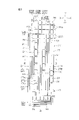
- FIG. 1 is an illustrative plan view showing an acceleration sensor according to an embodiment of the present disclosure
- FIG. FIG. 2 is a schematic plan view mainly showing the X-axis sensor.
- 3 is an enlarged plan view of a main part of FIG. 2.
- FIG. 4 is a schematic enlarged cross-sectional view taken along line IV-IV of FIG. 3.
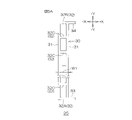
- FIG. 5A is a schematic enlarged plan view showing a spring portion used in the X-axis sensor shown in FIG. 3.
- FIG. 5B is an illustrative enlarged plan view showing a first modified example of the spring portion;
- FIG. 5C is an illustrative enlarged plan view showing a second modification of the spring portion.
- FIG. 5D is an illustrative enlarged plan view showing a spring portion used in the X-axis sensor according to the reference example shown in FIG. 6.
- FIG. FIG. 6 is an illustrative main part enlarged plan view showing a reference example of the X-axis sensor.
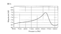
- FIG. 7A is a graph showing the relationship between vibration frequency and amplitude in the X-axis sensor of this embodiment.
- FIG. 7B is a graph showing the relationship between vibration frequency and amplitude in the X-axis sensor according to the reference example.
- FIG. 8 is a schematic plan view showing a modification of the X-axis sensor.
- FIG. 9A is an illustrative enlarged plan view showing a spring portion used in an X-axis sensor according to a modification; FIG.
- FIG. 9B is an illustrative enlarged plan view showing a reference example of the spring portion.
- FIG. 10 is a schematic plan view showing the Z-axis sensor.
- 11A is an enlarged plan view of a main part of FIG. 10.
- FIG. 11B is an enlarged plan view of a main part showing a reference example of the Z-axis sensor.
- FIG. 12 shows the positional relationship in the Z-axis direction between the fixed electrode and the movable electrode of the Z-axis sensor when acceleration in the Z-axis direction is acting, and the fixed electrode of the Z-axis sensor when acceleration in the Z-axis direction is acting. and a positional relationship in the Z-axis direction of the movable electrode.
- FIG. 10 is a schematic plan view showing the Z-axis sensor.
- 11A is an enlarged plan view of a main part of FIG. 10.
- FIG. 11B is an enlarged plan view of a main part showing a reference example of the Z-axis sensor.
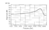
- FIG. 13A is a graph showing the relationship between vibration frequency and amplitude in the Z-axis sensor of this embodiment.
- FIG. 13B is a graph showing the relationship between vibration frequency and amplitude in the Z-axis sensor according to the reference example.
- FIG. 14 is a schematic plan view showing a modification of the Z-axis sensor.
- An embodiment of the present disclosure includes a semiconductor substrate having a cavity formed therein, a fixed structure including a fixed electrode supported by the semiconductor substrate in a state floating with respect to the cavity, and a fixed structure floating with respect to the cavity.
- a movable structure including a movable electrode supported by the semiconductor substrate via an elastic structure in a state and displaced relative to the fixed electrode, the elastic structure having a first end supported by the semiconductor substrate; a second end portion connected to the movable structure; and an intermediate portion connecting the first end portion and the second end portion; and the linear portion includes a plurality of linear frames extending parallel to each other in the direction in which the linear portion extends.
- the straight portion includes a plurality of reinforcing frames installed between the plurality of straight frames included in the straight portion.
- the linear portion includes a linear frame between the linear frames such that a triangular space is repeated along the linear frame. Includes multiple stiffening frames suspended.
- the linear portion includes a first linear portion and a second linear portion extending parallel to each other, and a third linear portion connecting one ends of the first linear portion and the second linear portion. including.
- each of said first straight portion, said second straight portion and said third straight portion includes at least one reinforcing frame spanning between said plurality of straight frames included therein. including.
- the linear portion includes a linear portion parallel to the extending direction of the movable electrode.
- the fixed electrode includes a pair of fixed electrodes extending parallel to each other in a second direction orthogonal to the first direction with an interval in a predetermined first direction
- the movable electrode includes a pair of movable electrodes disposed between said pair of fixed electrodes, spaced apart in said first direction and extending parallel to each other in said second direction.
- the fixed electrode includes a plurality of fixed electrodes formed in a comb shape in plan view
- the movable electrode includes a plurality of movable electrodes formed in a comb shape in plan view. an electrode pair, wherein the plurality of movable electrode pairs are disposed in non-contacting engagement with the plurality of fixed electrodes, each movable electrode pair being aligned with the fixed electrodes on opposite sides of the movable electrode pair; and extending parallel to each other.
- the cross-sectional shape of the fixed electrode and the cross-sectional shape of the movable electrode are squares elongated in the vertical direction.
- the elastic structure includes one straight portion and a tapered portion connected to one end of the straight portion, the straight portion consisting of two parallel straight frames.
- the tapered portion is formed from two connection frames extending obliquely outward with respect to the two linear frames such that the distance between the two connecting frames gradually widens from one end of each of the two linear frames.
- the linear portion is parallel to the extending direction of the movable electrode, or is a direction along the surface of the semiconductor substrate and orthogonal to the extending direction of the movable electrode. parallel to the direction.
- the fixed electrode includes a plurality of fixed electrodes formed in a comb shape in plan view
- the movable electrode includes a plurality of movable electrodes formed in a comb shape in plan view.
- the plurality of movable electrodes are arranged in non-contacting engagement with the plurality of fixed electrodes.
- the cross-sectional shape of the fixed electrode and the cross-sectional shape of the movable electrode are squares elongated in the vertical direction.
- one of the fixed electrode and the movable electrode is arranged in a downwardly displaced state with respect to the other.
- FIG. 1 is an illustrative plan view showing an acceleration sensor according to an embodiment of the present disclosure.
- the +X direction is a predetermined direction along the surface of the semiconductor substrate 2 in plan view
- the +Y direction is a direction along the surface of the semiconductor substrate 2 in plan view and orthogonal to the +X direction
- the +Z direction is a direction along the thickness of the semiconductor substrate 2 and perpendicular to the +X direction and the +Y direction.
- the -X direction is the direction opposite to the +X direction.
- the -Y direction is the opposite direction to the +Y direction.
- the -Z direction is the direction opposite to the +Z direction.
- the +X direction and the -X direction are collectively referred to as the "X-axis direction”.
- the +Y direction and the -Y direction are collectively referred to as the "Y-axis direction”.
- the +Z direction and the ⁇ Z direction are collectively referred to as the “Z-axis direction”.
- the acceleration sensor 1 includes a semiconductor substrate 2 having a square shape in plan view, a sensor section 3 arranged in the center of the semiconductor substrate 2, and electrode pads 4 arranged on the sides of the sensor section 3 on the semiconductor substrate 2. I'm in.
- the acceleration sensor 1 is a capacitive acceleration sensor.
- the semiconductor substrate 2 has a rectangular shape having two sides parallel to the X-axis direction and two sides parallel to the Y-axis direction in plan view.
- the sensor unit 3 has an X-axis sensor 5, a Y-axis sensor 6, and a Z-axis sensor 7 as sensors for detecting acceleration acting along three orthogonal axes in a three-dimensional space.
- the X-axis sensor 5 is for detecting acceleration acting in the X-axis direction.
- the Y-axis sensor 6 is for detecting acceleration in the Y-axis direction.
- the Z-axis sensor 7 is for detecting acceleration in the Z-axis direction.
- the semiconductor substrate 2 is made of a conductive silicon substrate (for example, a low resistance substrate having a resistivity of 5 ⁇ m to 500 ⁇ m).
- the semiconductor substrate 2 has a cavity 10 (see FIG. 4) inside, and an X-axis sensor 5, an X-axis sensor 5, and an X-axis sensor 5 are mounted on an upper wall (surface layer) 11 of the semiconductor substrate 2 having a top surface that partitions the cavity 10 from the surface side.
- a Y-axis sensor 6 and a Z-axis sensor 7 are formed.
- the X-axis sensor 5, the Y-axis sensor 6, and the Z-axis sensor 7 are part of the semiconductor substrate 2, and are attached to the bottom wall 12 (see FIG. 4) of the semiconductor substrate 2 having a bottom surface that defines the cavity 10 from the back side. It is supported in a floating state.
- the X-axis sensor 5 and the Y-axis sensor 6 are arranged adjacent to each other with an interval in the X-axis direction.
- Two Z-axis sensors 7 are arranged to surround each of the X-axis sensor 5 and the Y-axis sensor 6 .
- the Y-axis sensor 6 has substantially the same configuration as the X-axis sensor 5 rotated by 90° in plan view.
- a lid 8 made of, for example, a silicon substrate and bonded to the surface of the semiconductor substrate 2 .
- the electrode pads 4 are connected to external electronic components to input signals to the sensors 5-7 and output signals from the sensors 5-7. 1) is provided.
- the external electronic component is, for example, an ASIC (Application Specific Integrated Circuit) element.
- FIG. 2 is a schematic plan view mainly showing the X-axis sensor.
- 3 is an enlarged plan view of a main part of FIG. 2.
- FIG. 4 is a schematic enlarged cross-sectional view taken along line IV-IV of FIG. 3.
- FIG. 5A is a schematic enlarged plan view showing the spring portion of FIG. 3;
- a support portion 14 is formed between the X-axis sensor 5 and the Z-axis sensor 7 to support the X-axis sensor 5 in a floating state.
- the support portion 14 includes a support base portion 16 extending across the Z-axis sensor 7 toward the X-axis sensor 5 from the upper portion of one side wall 15 having a side surface that laterally partitions the cavity 10 of the semiconductor substrate 2; An annular portion 17 surrounding the sensor 5 is integrally included.
- the supporting portion 14 is supported by one side wall 15 of the semiconductor substrate 2 while floating from the bottom wall 12 of the semiconductor substrate 2 .
- the support base portion 16 has a rectangular shape elongated in the Y-axis direction in a plan view.
- the annular portion 17 has a rectangular annular shape in plan view, and includes a first frame portion 17A on the ⁇ Y side, a second frame portion 17B on the ⁇ X side, a third frame portion 17C on the +Y side, and a fourth frame portion 17D on the +X side. including.
- the first frame portion 17A is divided at the length center portion.
- a length center portion of the second frame portion 17B is connected to the support base portion 16 .
- the X-axis sensor 5 is arranged inside the annular portion 17 and supported by the annular portion 17 .
- the X-axis sensor 5 has a fixed structure 21 fixed to the support portion 14 provided in the cavity 10 and a movable structure 22 held vibratably with respect to the fixed structure 21 .
- the fixed structure 21 and the movable structure 22 are formed with the same thickness.
- the fixed structure 21 includes a fixed base portion 23 and a plurality of fixed electrodes 24 .
- the fixed base portion 23 extends in the X-axis direction along the inner wall of the first frame portion 17A and is fixed to the support portion 14 .
- the fixed base portion 23 has a ladder-like frame structure in a plan view, including a plurality of (two in this embodiment) main frames extending parallel to each other and a plurality of sub-frames installed between the plurality of main frames. doing.
- a plurality of fixed electrodes 24 are formed in a comb shape on the inner wall of the fixed base portion 23 .
- the plurality of fixed electrodes 24 are arranged parallel to each other at regular intervals in the X-axis direction. That is, the fixed electrodes 24 extend in the +Y direction from the fixed base portion 23 .
- the movable structure 22 includes a movable base portion 26 and a plurality of movable electrode portions 27 .
- the movable base portion 26 extends in the X-axis direction along the inner wall of the third frame portion 17C. Both ends of the movable base portion 26 are connected to the fixed base portion 23 via spring portions 25 that are extendable along the X-axis direction.
- the spring portion 25 is an example of the "elastic structure" of the present invention.
- the movable base portion 26 includes a plurality of (five in this embodiment) main frames 26A extending parallel to the X-axis direction, and a plurality of sub-frames 26B installed between the plurality of main frames 26A. It has a shaped frame structure.
- a plurality of movable electrode portions 27 are formed in a comb shape on the inner wall of the movable base portion 26 .
- the plurality of movable electrode portions 27 are arranged parallel to each other at equal intervals in the X-axis direction.
- a plurality of movable electrode portions 27 extend from the movable base portion 26 toward between the fixed electrodes 24 adjacent to each other. That is, the comb tooth-shaped movable electrode portion 27 is arranged so as to mesh with the comb tooth-shaped fixed electrode 24 without coming into contact with the fixed electrode 24 .
- Each movable electrode portion 27 includes a first movable electrode 27A and a second movable electrode 27B extending parallel to each other in the ⁇ Y direction from the ⁇ Y side ends of a pair of adjacent sub-frames 26B in the movable base portion 26, and and a plurality of connecting portions 27C that connect the .
- a length intermediate portion of each connecting portion 27C is constituted by a first isolated coupling portion (insulating layer) 91 made of silicon oxide (SiO 2 ).
- the first movable electrode 27A and the second movable electrode 27B are electrically insulated.
- the first movable electrode 27A and the second movable electrode 27B included in the movable electrode portion 27 are examples of the "movable electrode pair" of the present invention.
- the cross-sectional shape of the fixed electrode 24 and the movable electrodes 27A and 27B is, as shown in FIG. 4, a rectangular shape elongated in the Z-axis direction.
- the fixed electrode 24 and the movable electrodes 27A and 27B are plate-shaped with the thickness direction being the X-axis direction.
- first movable subframe 26Ba the subframe to which the first movable electrode 27A is connected
- second movable subframe 26Bb the subframe to which the second movable electrode 27B is connected
- a second isolating joint (insulating layer) 92 made of silicon oxide is formed in the main frame 26A at the intermediate length of the portion connecting two adjacent sub-frames 26B. Therefore, each subframe 26B is electrically isolated from other subframes 26B.
- Each movable electrode 27A, 27B is electrically insulated from the other movable electrodes 27A, 27B by the first isolation joint 91 and the second isolation joint 92 .
- the first movable electrode 27A is arranged on the -X side with respect to the second movable electrode 27B.
- the distance between the first movable electrode 27A and the fixed electrode 24 adjacent thereto is equal to the distance between the second movable electrode 27B and the fixed electrode 24 adjacent thereto.
- the -Y side ends of the spring portion 25 arranged on the -X side and the spring portion 25 arranged on the +Y side are constituted by a third isolation coupling portion (insulating layer) 93 made of silicon oxide in the middle of the length. It is mechanically connected to the fixed base portion 23 via the connecting frame. Therefore, the fixed base portion 23 and the spring portion 25 are electrically insulated.
- the +Y side end of the spring portion 25 arranged on the -X side is mechanically and electrically connected to the first movable sub-frame 26Ba on the most -X side.
- the +Y side end of the spring portion 25 arranged on the +X side is mechanically and electrically connected to the second movable sub-frame 26Bb on the most +X side.
- These spring portions 25 function as springs that support the movable base portion 26 so as to be movable in the X-axis direction, and also function as conductive paths.
- An insulating film (not shown) is formed on the surface of the semiconductor substrate 2 including the fixed structure 21 and the movable structure 22 .
- a plurality of wirings (not shown) are formed on the surface of the insulating film.
- the plurality of wirings are the first wiring for electrically connecting the plurality of fixed electrodes 24 to the electrode pad 4 for the fixed electrode, and the plurality of first movable electrodes 27A for electrically connecting the electrode pad 4 for the first movable electrode. and a third wiring for electrically connecting the plurality of second movable electrodes 27B to the electrode pads 4 for the second movable electrodes.
- the second wiring is wiring for electrically connecting the plurality of first movable sub-frames 26Ba to each other and wiring for electrically connecting the -X side spring portion 25 to the electrode pad 4 for the first movable electrode.
- the third wiring includes wiring for electrically connecting the plurality of second movable sub-frames 26Bb to each other and wiring for electrically connecting the spring portion 25 on the +X side to the electrode pad 4 for the second movable electrode.
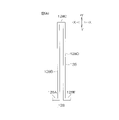
- the lengths of the X-axis sensor 5 in the X-axis direction and the Y-axis direction are, for example, about 300 ⁇ m.
- the length in the Z-axis direction from the +Z-side surface of the X-axis sensor 5 to the inner surface (+Z-side surface) of the bottom wall 12 (see FIG. 4) of the semiconductor substrate 2 is, for example, about 50 ⁇ m.
- the length in the Z-axis direction from the +Z-side surface of the X-axis sensor 5 to the outer surface (-Z-side surface) of the bottom wall 12 of the semiconductor substrate 2 is, for example, about 200 ⁇ m to 300 ⁇ m.
- the lengths of the fixed electrode 24, the first movable electrode 27A and the second movable electrode 27B in the Z-axis direction are, for example, about 15 ⁇ m to 30 ⁇ m.
- the movable base portion 26 supported by the two spring portions 25 vibrates in the X-axis direction.
- the first movable electrode 27A and the second movable electrode 27B extending from the movable base portion 26 also vibrate in the X-axis direction between the two fixed electrodes 24 adjacent to each other.
- the movable base portion 26 moves in the +X direction
- the first movable electrode 27A moves away from the adjacent fixed electrode 24, and the second movable electrode 27B moves closer to the adjacent fixed electrode 24.
- the first movable electrode 27A moves closer to the adjacent fixed electrode 24, and the second movable electrode 27B moves away from the adjacent fixed electrode 24.
- the facing distance d1 between the first movable electrode 27A and the fixed electrode 24 adjacent thereto and the facing distance d2 between the second movable electrode 27B and the fixed electrode 24 adjacent thereto change.
- a change in capacitance C1 between the first movable electrode 27A/fixed electrode 24 due to a change in the facing distance d1 and a change in capacitance C1 between the second movable electrode 27B/fixed electrode 24 due to a change in the facing distance d2 Acceleration in the X-axis direction is detected by detecting a change in C2.
- the -X side spring portion 25 is composed of a straight portion 30 extending in the Y-axis direction.
- the straight portion 30 includes two straight frames 31 extending in parallel in the Y-axis direction and a plurality of reinforcing frames 32 installed between the straight frames 31 .
- a first connecting portion 33 extending in the +X direction is connected to the +X side end of the first reinforcing frame 32A.
- a second connecting portion 34 extending in the +X direction is connected to the +X side end of the second reinforcing frame 32B.
- the ⁇ Y side end of the spring portion 25 (linear portion 30 ) is mechanically connected to the fixed base portion 23 via the first connection portion 33 .
- the +Y side end of the spring portion 25 (linear portion 30) is mechanically and electrically connected to the first movable sub-frame 26Ba via the second connection portion .
- the spring portion 25 arranged on the +X side is located at the -X side spring portion 25 with respect to a straight line passing through the center between the -X side spring portion 25 and the +X side spring portion 25 and extending in the Y-axis direction. It has a planar shape that is symmetrical with Therefore, in the +X side spring portion 25, the first connecting portion 33 extending in the -X direction is connected to the -X side end of the first reinforcing frame 32A, and the -X side end of the second reinforcing frame 32B is connected to A second connecting portion 34 extending in the -X direction is connected.
- the ⁇ Y side end of the +X side spring portion 25 (linear portion 30 ) is mechanically connected to the fixed base portion 23 via the first connection portion 33 .
- the +Y side end of the +X side spring portion 25 (linear portion 30) is mechanically and electrically connected to the second movable sub-frame 26Bb via the second connection portion .
- FIG. 6 is an illustrative main part enlarged plan view showing a reference example of the X-axis sensor.
- the same reference numerals as in FIG. 3 denote the parts corresponding to the parts in FIG. 3 described above.
- 5D is an illustrative enlarged plan view showing a spring portion used in the X-axis sensor according to the reference example shown in FIG. 6.
- the -X side spring portion 125 used in the X-axis sensor 105 is composed of a linear portion 131 made up of a single linear frame extending in the Y-axis direction.
- a first connecting portion 132 extending in the +X direction from the -Y direction end of the straight portion 131 is connected to the -Y direction end of the straight portion 131 .
- the +Y direction end of the straight portion 131 is connected to a hook-shaped second connection portion 133 extending in the -Y direction after extending in the +X direction from the +Y direction end of the straight portion 131 .
- the ⁇ Y side end of the spring portion 125 (linear portion 131 ) is mechanically connected to the fixed base portion 23 via the first connection portion 132 .
- the +Y side end of the spring portion 125 (linear portion 131) is mechanically and electrically connected to the second movable sub-frame 26Bb via the second connection portion 133. As shown in FIG.
- the spring portion 125 arranged on the +X side is located on the -X side with respect to a straight line passing through the center between the -X side spring portion 125 and the -X side spring portion 125 and extending in the Y-axis direction. 125 and has a plane shape of line symmetry.
- a first connection portion 132 extending in the -X direction is connected to the -Y side end of a straight portion 131 made of one straight frame, and the +Y side end of the straight portion 131 is connected to the -Y side end.
- a hook-shaped second connecting portion 133 extending in the -Y direction is connected.
- the ⁇ Y side end of the +X side spring portion 125 (linear portion 131 ) is mechanically connected to the fixed base portion 23 via the first connection portion 132 .
- the +Y side end of the +X side spring portion 125 (linear portion 131) is mechanically and electrically connected to the first movable sub-frame 26Ba via a second connection portion 133. As shown in FIG.
- the width of the linear portion 30 can be made larger than in the spring portion 125 of the X-axis sensor 105 according to the reference example. That is, the width W1 (see FIG. 5A) of the linear portion 30 of the spring portion 25 can be made larger than the width W2 (see FIG. 5D) of the linear portion 131 of the spring portion 125. As shown in FIG. Thereby, the resonance frequency of the movable portion of the X-axis sensor 5 can be increased. This makes it possible to widen the range of detectable acceleration.
- FIG. 7A is a graph showing the relationship between vibration frequency and amplitude in the X-axis sensor 5 of this embodiment.
- FIG. 7B is a graph showing the relationship between vibration frequency and amplitude in the X-axis sensor 105 according to the reference example.
- the X-axis sensor 5 of this embodiment can increase the resonance frequency of the movable portion compared to the X-axis sensor 105 according to the reference example.
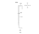
- FIG. 5B is an illustrative plan view showing a first modification of the spring portion arranged on the -X side.
- the ⁇ X side spring portion 25A shown in FIG. 5B consists of a linear portion 30A extending parallel to the Y-axis direction.
- the linear portion 30A includes two linear frames 31 extending parallel to the Y-axis direction, a first reinforcing frame 32A connecting the -Y side ends of the linear frames 31, and the +Y side ends of the linear frames 31. and a second reinforcing frame 32B.
- the straight portion 30A includes a third reinforcing frame 32D that reinforces the straight frames 31 so that triangular spaces are repeated along the straight frames 31 between the two straight frames 31. As shown in FIG.
- a first connecting portion 33 extending in the +X direction is connected to the +X side end of the first reinforcing frame 32A.
- a second connecting portion 34 extending in the +X direction is connected to the +X side end of the second reinforcing frame 32B.
- the ⁇ Y side end of the spring portion 25A (linear portion 30A) is mechanically connected to the fixed base portion 23 via the first connection portion 33 .
- the +Y side end of the spring portion 25A (linear portion 30A) is mechanically and electrically connected to the first movable sub-frame 26Ba via the second connection portion .
- the spring portion 25A arranged on the +X side is the -X side spring with respect to a straight line extending in the Y-axis direction passing through the center between the -X side spring portion 25A and the +X side spring portion 25A. It has a planar shape line-symmetrical to the portion 25A. Therefore, in the +X side spring portion 25A, the first connection portion 33 extending in the -X direction is connected to the -X side end of the first reinforcing frame 32A, and the -X side end of the second reinforcing frame 32B The second connecting portion 34 extending in the -X direction is connected.
- the ⁇ Y side end of the +X side spring portion 25A (linear portion 30A) is mechanically connected to the fixed base portion 23 via the first connection portion 33 .
- the +Y side end of the +X side spring portion 25A (linear portion 30A) is mechanically and electrically connected to the second movable sub-frame 26Bb via the second connection portion 34 .
- FIG. 5C is an illustrative plan view showing a second modification of the spring portion arranged on the -X side.
- the ⁇ X side spring portion 25B shown in FIG. 5C consists of a straight portion 30B extending parallel to the Y-axis direction.
- the straight portion 30B includes three straight frames 31 extending in parallel in the Y-axis direction and a plurality of reinforcing frames 32 installed between the straight frames 31 .
- the reinforcing frames 32 include a first reinforcing frame 32A connecting the ends of the three linear frames 31 in the -Y direction, and a second reinforcing frame 32B connecting the ends of the three linear frames 31 in the +Y direction. and a plurality of third reinforcing frames 32C that connect the lengthwise intermediate portions of the straight frames 31 to each other.
- a first connecting portion 33 extending in the +X direction is connected to the +X side end of the first reinforcing frame 32A.
- a second connecting portion 34 extending in the +X direction is connected to the +X side end of the second reinforcing frame 32B.
- the ⁇ Y side end of the spring portion 25B (straight portion 30B) is mechanically connected to the fixed base portion 23 via the first connection portion 33 .
- the +Y side end of the spring portion 25B (linear portion 30B) is mechanically and electrically connected to the first movable sub-frame 26Ba via the second connection portion .
- the spring portion 25B arranged on the +X side is arranged on the -X side with respect to a straight line passing through the center between the -X side spring portion 25B and the +X side spring portion 25B and extending in the Y-axis direction. It has a planar shape that is symmetrical with Therefore, in the +X side spring portion 25B, the first connecting portion 33 extending in the -X direction is connected to the -X side end of the first reinforcing frame 32A, and the -X side end of the second reinforcing frame 32B The second connecting portion 34 extending in the -X direction is connected.
- the ⁇ Y side end of the +X side spring portion 25B (linear portion 30B) is mechanically connected to the fixed base portion 23 via the first connection portion 33 .
- the +Y side end of the +X side spring portion 25B (linear portion 30B) is mechanically and electrically connected to the second movable sub-frame 26Bb via the second connection portion 34 .
- Y-axis sensor 6 has substantially the same configuration as the X-axis sensor 5 rotated by 90° in plan view, so detailed description thereof will be omitted.
- the fixed electrode 24, the first movable electrode 27A, and the second movable electrode 27B each extend in the X-axis direction. vibrate in one direction.
- the first movable electrode 27A and the second movable electrode 27B also vibrate in the Y-axis direction between the two fixed electrodes 24 adjacent to each other.
- FIG. 8 is a schematic plan view showing a modification of the X-axis sensor.
- the X-axis sensor 5A has a fixed structure 21 fixed to the semiconductor substrate 2 and a movable structure 22 held vibratably with respect to the fixed structure 21 .
- the fixed structure 21 and the movable structure 22 are formed with the same thickness.
- the fixed structure 21 and the movable structure 22 are supported by the semiconductor substrate 2 while floating from the bottom wall of the semiconductor substrate 2 .
- the fixed structure 21 includes a fixed base portion 23 and a plurality of fixed electrodes 24 .
- the fixed base portion 23 has a quadrangular annular shape in a plan view, and is arranged so as to surround the periphery of the arrangement area of the X-axis sensor 5A.
- the fixed base portion 23 includes a -Y side first frame portion 23A, a -X side second frame portion 23B, a +Y side third frame portion 23C, and a -X side fourth frame portion 23D.
- a length center portion of the second frame portion 23B and a length center portion of the fourth frame portion 23D are supported by the semiconductor substrate 2 .
- Each of the frame portions 23A to 23D of the fixed base portion 23 includes a plurality of (two in the example of FIG. 8) main frames extending parallel to each other, and a plurality of sub-frames bridged between the plurality of main frames in plan view. It has a ladder-like frame structure.
- the plurality of fixed electrodes 24 includes a plurality of first fixed electrodes 24A formed in a comb-like shape on the inner wall of the first frame portion 23A, and a plurality of comb-like fixed electrodes 24A formed in a comb-like shape on the inner wall of the third frame portion 23C. and a second fixed electrode 24B.
- the plurality of first fixed electrodes 24A extend from the first frame portion 23A to the vicinity of the central portion in the Y-axis direction of the arrangement area of the X-axis sensor 5A.
- the plurality of second fixed electrodes 24B extend from the third frame portion 23C to the vicinity of the central portion in the Y-axis direction of the arrangement area of the X-axis sensor 5A.
- the plurality of first fixed electrodes 24A extend parallel to each other in the +Y direction from the first frame portion 23A at equal intervals in the X-axis direction.
- the plurality of second fixed electrodes 24B extend parallel to each other in the -Y direction from the third frame portion 23C at equal intervals in the X-axis direction.
- the movable structure 22 includes a movable base portion 26 and a plurality of movable electrode portions 27 .
- the movable base portion 26 extends in the X-axis direction at the central portion in the Y-axis direction of the arrangement area of the X-axis sensor 5A, and both ends of the movable base portion 26 are fixed to the fixed base portion 23 via spring portions 28 that are elastic in the X-axis direction. It is
- the spring portion 28 is an example of the "elastic structure" of the present invention.
- the movable base portion 26 consists of a plurality of (four in this embodiment) frames extending parallel to the X-axis direction, and both ends thereof are connected to the spring portions 28 .
- Two spring portions 28 are provided at each end of the movable base portion 26 .
- a plurality of movable electrode portions 27 are formed in a comb shape on each side wall of the movable base portion 26 .
- the plurality of movable electrode portions 27 extend across the movable base portion 26 toward between the first fixed electrodes 24A adjacent to each other and between the second fixed electrodes 24B adjacent to each other.
- the comb tooth-shaped movable electrode portion 27 extending from the movable base portion 26 to the -Y side is arranged so as to mesh with the first comb tooth-shaped fixed electrode 24A without coming into contact with the first fixed electrode 24A.
- the comb-teeth-shaped movable electrode portion 27 extending from the movable base portion 26 toward the +Y side is arranged so as to mesh with the comb-teeth-shaped second fixed electrode 24B without contacting the second fixed electrode 24B.
- Each movable electrode portion 27 includes a first movable electrode 27A and a second movable electrode 27B extending parallel to each other in the Y-axis direction at intervals in the X-axis direction, and a plurality of connecting portions 27C connecting them.
- a lengthwise intermediate portion of each connecting portion 27C is constituted by an isolated joint portion (not shown) made of silicon oxide.
- the first movable electrode 27A and the second movable electrode 27B included in the movable electrode portion 27 are examples of the "movable electrode pair" of the present invention.
- the first movable electrode 27A is arranged on the -X side with respect to the second movable electrode 27B.
- the distance between the first movable electrode 27A and the adjacent first fixed electrode 24A or the second fixed electrode 24B is the distance between the second movable electrode 27B and the adjacent second movable electrode 27B. It is equal to the distance between the first fixed electrode 24A and the second fixed electrode 24B.
- Each first movable electrode 27A is electrically insulated from the other first movable electrodes 27A and second movable electrodes 27B at the movable base portion 26.
- Each second movable electrode 27B is electrically insulated from the other second movable electrodes 27B and the first movable electrodes 27A at the movable base portion 26 .
- the two spring portions 28 arranged on the -X side are connected to the first movable electrode 27A arranged on the most -X side in the movable base portion 26 .
- the two spring portions 28 arranged on the +X side are connected to the second movable electrode 27B arranged on the most +X side in the movable base portion 26 .
- the four spring portions 28 function as springs that support the movable base portion 26 so as to be movable in the X-axis direction, and also function as conductive paths.
- An insulating film (not shown) is formed on the surface of the semiconductor substrate 2 including the fixed structure 21 and the movable structure 22 .
- a wiring (not shown) is formed on the surface of the insulating film.
- the wires are first wires for electrically connecting the plurality of first fixed electrodes 24A and the plurality of second fixed electrodes 24B to the electrode pads 4 for fixed electrodes, and the plurality of first movable electrodes 27A are connected to the first movable electrodes 27A. and a third wiring for electrically connecting the plurality of second movable electrodes 27B to the electrode pad 4 for the second movable electrode.
- the movable base portion 26 supported by the four spring portions 28 vibrates in the X-axis direction.
- the first movable electrode 27A and the second movable electrode 27B extending from the movable base portion 26 are also arranged between two adjacent first fixed electrodes 24A and between two adjacent second fixed electrodes 24B. Vibrate axially.
- FIG. 9A is a schematic plan view showing the spring portion 28 arranged on the +Y side on the -X side.
- the spring portion 28 has a vertically elongated U shape opening downward in plan view. Specifically, the spring portion 28 is arranged on the +X side of the first linear portion 28B and the first linear portion 28B extending in the Y-axis direction in plan view, and parallel to the first linear portion 28B. and a third straight portion (connecting portion) 28C that connects the +Y direction ends of the first straight portion 28B and the second straight portion 28D.
- the spring portion 28 further includes a first connecting portion 28A extending in the -X direction from the -Y side end of the first straight portion 28B and a second connecting portion 28A extending in the +X direction from the -Y side end of the second straight portion 8D. and part 28E.
- the first connection portion 28A, the first straight portion 28B, the third connection portion 28C, the second straight portion 28D and the second connection portion 28E each include two straight frames 35 extending parallel to each other.
- the first linear portion 28B, the third connecting portion 28C and the second linear portion 28D include one or more reinforcing frames 36 installed between the linear frames 35. As shown in FIG.
- a first end of the spring portion 28 (-Y side end of the first linear portion 28B) is mechanically connected to the second frame portion 23B of the fixed base portion 23 via a first connection portion 28A.
- the second end of the spring portion 28 (-Y side end of the second linear portion 28D) is mechanically and electrically connected to the movable base portion 26 via the second connection portion 28E.
- the spring portion 28 arranged on the -Y side on the -X side passes through the center between the +Y side spring portion 28 on the -X side and the -Y side spring portion 28 on the -X side and extends in the X-axis direction. It has a plane shape symmetrical to the spring portion 28 on the +Y side on the -X side with respect to the extending straight line.
- a first end of the spring portion 28 (+Y side end of the first linear portion 28B) is mechanically connected to the second frame portion 23B of the fixed base portion 23 via a first connection portion 28A. .
- the second end of the spring portion 28 (+Y side end of the second linear portion 28D) is mechanically and electrically connected to the movable base portion 26 via the second connection portion 28E.
- the two spring portions 28 on the +X side are located on the -X side with respect to a straight line passing through the center between the two spring portions 28 on the -X side and the two spring portions 28 on the +X side and extending in the Y-axis direction. It has a planar shape line-symmetrical to the two spring portions 28 .
- FIG. 9B is an illustrative plan view showing a reference example of the spring portion arranged on the +Y side on the -X side.
- the overall shape of the spring portion 128 of the reference example is the same as the spring portion 28 of FIG. It consists of two straight portions 128D and a second connecting portion 128E. However, in the spring portion 128 of the reference example, each of these portions 128A to 128E is composed of one linear frame 135 respectively.
- the widths of the linear portions 28B to 28D can be increased compared to the spring portion 128 of the reference example. That is, the width of the linear portions 28B-28D of the spring portion 28 can be made larger than the width of the linear portions 128B-128D of the spring portion 128.
- the resonance frequency of the movable portion can be increased compared to the X-axis sensor using the spring portion 128 of the reference example. This makes it possible to widen the range of detectable acceleration.
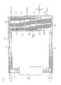
- FIG. 10 is a schematic plan view showing the Z-axis sensor.
- 11A is an enlarged plan view of a main part of FIG. 10.
- FIG. 10 is a schematic plan view showing the Z-axis sensor.
- the semiconductor substrate 2 has the cavity 10 (see FIG. 4) inside, as described above.
- a supporting portion 14 supports the X-axis sensor 5 and the Y-axis sensor 6 in a floating state with respect to the bottom wall 12 (see FIG. 4) of the semiconductor substrate 2 so as to surround each of them.
- a Z-axis sensor 7 is arranged.
- the Z-axis sensor 7 has a fixed structure 51 fixed to the support portion 14 (support base portion 16) provided in the cavity 10, and a movable structure 52 held vibratably with respect to the fixed structure 51. ing.
- the fixed structure 51 and the movable structure 52 are formed with the same thickness.
- the fixing structure 51 is arranged so as to surround the X-axis sensor 5 (more specifically, the annular portion 17 of the supporting portion 14 described above).
- a movable structure 52 is arranged so as to further surround it.
- the fixed structure 51 and the movable structure 52 are integrally connected to the side wall on the ⁇ Y side and the side wall on the +Y side of the supporting base portion 16 .
- the Z-axis sensor 7 arranged to surround the Y-axis sensor 6 is arranged so that the movable structure 52 surrounds the Y-axis sensor 6 (not shown).
- a fixed structure 51 is arranged.
- the fixed structure 51 includes a fixed base portion 53 having a quadrangular annular shape in a plan view and fixed to the support base portion 16 .
- the fixed base portion 53 includes a ⁇ Y side frame portion, a ⁇ X side frame portion, a +Y side frame portion, and a +X side frame portion.
- the fixed structure 51 further includes a fixed electrode structure provided on the +X side frame portion of the fixed base portion 53 .
- Each frame portion of the fixed base portion 53 has a ladder-like frame structure in a plan view including a plurality of linear main frames extending parallel to each other and a plurality of sub-frames installed between the plurality of main frames. ing.
- the fixed electrode structure includes multiple fixed backbones 55 and multiple fixed electrodes 56 .
- a plurality of fixed core portions 55 are arranged in a comb shape on the outer wall of the +X side frame portion of the fixed base portion 53 .
- the plurality of fixed core portions 55 extend parallel to each other in the +X direction from the +X side frame portion of the fixed base portion 53 at equal intervals in the Y-axis direction.
- a plurality of fixed electrodes 56 are formed in a comb shape on both side walls of each fixed base portion 55 .
- the comb-shaped fixed electrodes 56 extend parallel to each other in the Y-axis direction from both side walls of the fixed base portion 55 at equal intervals in the X-axis direction.
- the movable structure 52 includes a movable base portion 57 having a quadrangular annular shape in plan view.
- the movable base portion 57 includes a ⁇ Y side frame portion ( ⁇ Y side straight portion), a ⁇ X side frame portion ( ⁇ X side straight portion), a +Y side frame portion (+Y side straight portion), and a +X side frame portion. part (+X side straight part).
- the ⁇ X side frame portion ( ⁇ X side linear portion) of the movable base portion 57 is connected to the ⁇ X side frame portion of the fixed base portion 53, the ⁇ X side frame portion of the movable base portion 57
- the portion ( ⁇ X side linear portion) can also be regarded as part of the fixed base portion 53 .
- the movable base portion 57 is composed of the -Y side straight portion, the +Y side straight portion, and the +X side straight portion connecting the +X side ends thereof.
- the movable structure 52 further includes a +X side frame portion (+X side linear portion) of the movable base portion 57, a +X side end portion of the ⁇ Y side frame portion ( ⁇ Y side linear portion), and a +Y side frame portion (+Y side linear portion ) and a movable electrode structure formed on the +X side end of the .
- the movable electrode structure includes multiple movable backbones 59 and multiple movable electrodes 60 .
- a plurality of movable core portions 59 are formed in a comb shape on the inner wall of the +X side frame portion of the movable base portion 57 .
- a plurality of movable core portions 59 extend from the +X side frame portion of the movable base portion 57 toward between the fixed core portions 55 adjacent to each other.
- the comb tooth-shaped movable trunk portion 59 is arranged so as to mesh with the comb tooth-shaped fixed trunk portion 55 without coming into contact with the fixed trunk portion 55 .
- the plurality of movable electrodes 60 are formed in a comb-like shape on the inner wall of the -Y side frame portion of the movable base portion 57 and the plurality of first movable electrodes 60A formed in a comb-like shape on both side walls of the movable base portion 59. and a third movable electrode 60C formed in a comb shape on the inner wall of the +Y side frame portion of the movable base portion 57 .
- the plurality of first movable electrodes 60A extend from both side walls of the movable core 59 toward between the fixed electrodes 56 adjacent to each other.
- the plurality of second movable electrodes 60B extend from the -Y side frame portion of the movable base portion 57 toward between the fixed electrodes 56 adjacent to each other.
- the plurality of third movable electrodes 60C extend from the +Y side frame portion of the movable base portion 57 toward between the fixed electrodes 56 adjacent to each other.
- the plurality of movable electrodes 60 extend in the Y-axis direction.
- the comb-teeth-shaped movable electrode 60 is arranged so as to mesh with the comb-teeth-shaped fixed electrode 56 without coming into contact with the fixed electrode 24 .
- Each frame portion of the movable base portion 57 has a ladder-like frame structure in a plan view including a plurality of linear main frames extending parallel to each other and a plurality of sub-frames installed between the plurality of main frames. ing.
- the -Y side end portion of the -X side frame portion of the movable base portion 57 and the -X side end portion of the -Y side frame portion of the movable base portion 57 are connected via the -Y side spring portion 61.
- the +Y side end of the ⁇ X side frame portion of the movable base portion 57 and the ⁇ X side end portion of the +Y side frame portion of the movable base portion 57 are connected via the +Y side spring portion 61 .
- the spring portion 61 is an example of the "elastic structure" of the present invention.
- the +Y side spring portion 61 is composed of a linear portion 61A extending in the Y-axis direction and a tapered portion 61B formed at the -Y side end of the linear portion 61A.
- the straight portion 61A consists of two straight frames 62 extending parallel to each other in the Y-axis direction.
- the tapered portion 61B is composed of two inclined frames 63 extending obliquely outward from the two linear frames 62 from the -Y side ends of the two linear frames 62 so that the distance between them gradually widens. .
- the first end of the spring portion 61 (the -Y side end of the tapered portion 61B) is supported by the support base portion 16 via the -X side frame portion of the movable base portion 57. As shown in FIG.
- the second end of the spring portion 61 (the +Y side end of the straight portion 61A) is mechanically and electrically connected to the ⁇ X side end of the +Y side frame portion of the movable base portion 57 .
- the ⁇ Y side spring portion 61 is symmetrical with the +Y side spring portion 61 with respect to a straight line passing through the center between the +Y side spring portion 61 and the ⁇ Y side spring portion 61 and extending in the X-axis direction. It has a planar shape of The ⁇ Y side spring portion 61 is composed of a linear portion 61A extending in the Y-axis direction and a tapered portion 61B formed at the +Y side end of the linear portion 61A.
- the straight portion 61A consists of two straight frames 62 extending parallel to each other in the Y-axis direction.
- the tapered portion 61B is composed of two inclined frames 63 extending obliquely outward from the two linear frames 62 from the +Y side ends of the two linear frames 62 so that the distance between them gradually widens.
- the first end of the -Y side spring portion 61 (the +Y side end of the tapered portion 61B) is supported by the support base portion 16 via the -X side frame portion of the movable base portion 57 .
- the second end of the -Y side spring portion 61 (the -Y side end of the linear portion 61A) is mechanically and electrically connected to the -X side end of the -Y side frame portion of the movable base portion 57.
- the two spring portions 61 function as springs for making the movable electrode 60 movable in the Z-axis direction.
- the spring portion 61 is elastically distorted, and the movable base portion 57 is moved as if it were a pendulum, with the spring portion 61 as a fulcrum, and the bottom wall 12 of the semiconductor substrate 2 (see FIG. 4).
- the movable electrode 60 meshing with the fixed electrode 56 in a comb-teeth shape vibrates in the Z-axis direction.
- the movable electrode 60 vibrates in the Z-axis direction.
- the area of the overlapping region of the facing surfaces of the movable electrode 60 and the fixed electrode 56 changes. Acceleration acting in the Z-axis direction can be detected by electrically detecting a change in capacitance due to a change in the area.
- the Z-axis sensor 7 arranged to surround the X-axis sensor 5 will be referred to as the "first Z-axis sensor 7A”
- the Z-axis sensor 7 arranged to surround the Y-axis sensor 6 will be referred to as the "second Z-axis sensor 7A”.
- sensor 7B the Z-axis sensor 7 arranged to surround the X-axis sensor 5
- the fixed structure 51 arranged inside the movable structure 52 is affected by the silicon oxide film (not shown) formed on the surface of the fixed base portion 53, and the fixed electrode structure is It is warped so that it hangs down on the -Z side.
- the movable structure 52 arranged inside the fixed structure 51 is affected by the silicon oxide film (not shown) formed on the surface of the movable base portion, and the movable electrode structure is shifted to the -Z side. It is warped as if it were hanging down.
- FIG. 12 shows the positional relationship in the Z-axis direction between the fixed electrode and the movable electrode of the Z-axis sensor when acceleration in the Z-axis direction does not act, and the fixed electrode of the Z-axis sensor when acceleration in the Z-axis direction acts. and a positional relationship in the Z-axis direction of the movable electrode.
- F denotes the fixed electrode
- M denotes the movable electrode.
- FIG. 12 shows the positional relationship in the Z-axis direction between the fixed electrode F and the movable electrode M when no acceleration in the Z-axis direction acts on the acceleration sensor 1 in the first Z-axis sensor 7A. .
- FIG. 12 shows the positional relationship in the Z-axis direction between the fixed electrode F and the movable electrode M when no acceleration in the Z-axis direction acts on the acceleration sensor 1 in the second Z-axis sensor 7B. .
- FIG. 12 shows the positional relationship in the Z-axis direction between the fixed electrode F and the movable electrode M of the first Z-axis sensor 7A when acceleration in the +Z direction acts on the acceleration sensor 1 .
- the lower right of FIG. 12 shows the positional relationship in the Z-axis direction between the fixed electrode F and the movable electrode M of the second Z-axis sensor 7B when +Z-direction acceleration acts on the acceleration sensor 1 .
- the fixed electrode F is arranged at a position shifted to the -Z side with respect to the movable electrode M.
- the movable electrode M is arranged at a position shifted to the -Z side with respect to the fixed electrode F.
- the movable electrode M moves in the -Z direction with respect to the fixed electrode F, as shown in FIG.
- the capacitance C1 between the fixed electrode F and the movable electrode M increases in the first Z-axis sensor 7A
- the capacitance C2 between the fixed electrode F and the movable electrode M increases in the second Z-axis sensor 7B. Decrease.
- the Z Axial acceleration is detected.
- FIG. 11B is an enlarged plan view of a main part showing a reference example of the Z-axis sensor.
- the same reference numerals as those of FIG. 11A are used for the portions corresponding to the respective portions of FIG. 11A described above.
- the Z-axis sensor 107 shown in FIG. 11B has a structure similar to that of the Z-axis sensor 7 described above, but differs from the Z-axis sensor 7 described above in the structure of the spring portion and its vicinity.
- the ⁇ X side frame portion of the movable base portion 57 is composed of one main frame.
- the +Y side end portion of the ⁇ X side frame portion of the movable base portion 57 is connected to the +Y side frame portion of the movable base portion 57 via the +Y side spring portion 161
- the ⁇ X side frame portion of the movable base portion 57 is connected to the +Y side frame portion of the movable base portion 57 via the spring portion 161 on the +Y side.
- the ⁇ Y side end portion is connected to the ⁇ Y side frame portion of the movable base portion 57 via a ⁇ Y side spring portion 161 having the same configuration as the spring portion 161 .
- the spring portion 161 on the +Y side is composed of a linear portion 162 consisting of a single linear frame extending in the Y-axis direction.
- a first end portion of the spring portion 161 (the ⁇ Y side end portion of the straight portion 162 ) is supported by the support base portion 16 via the ⁇ X side frame portion of the movable base portion 57 .
- a second end of the spring portion 161 (the +Y side end of the linear portion 162 ) is mechanically and electrically connected to the +Y side frame portion of the movable base portion 57 .
- the ⁇ Y side spring portion 161 is symmetrical with the +Y side spring portion 161 with respect to a straight line passing through the center between the +Y side spring portion 161 and the ⁇ Y side spring portion 161 and extending in the X-axis direction. It has a planar shape of The ⁇ Y side spring portion 161 is composed of a linear portion 162 formed of one linear frame extending in the Y-axis direction. A first end of the -Y side spring portion 161 (the +Y side end of the linear portion 162) is supported by the support base portion 16 via the -X side frame portion of the movable base portion 57. FIG. The second end of the spring portion 161 (the ⁇ Y side end of the straight portion 162 ) is mechanically and electrically connected to the ⁇ Y side frame portion of the movable base portion 57 .
- the width of the frame used for the spring part is limited. Therefore, in the spring portion 61 used in the Z-axis sensor 7 of the present embodiment, the width of the linear portion 61A can be increased compared to the spring portion 161 used in the Z-axis sensor 107 of the reference example. That is, the width of the linear portion 61A of the spring portion 61 can be made larger than the width of the linear portion 162 of the spring portion 161. As shown in FIG. Thereby, in the Z-axis sensor 7 of the present embodiment, the resonance frequency of the movable portion can be increased as compared with the Z-axis sensor 107 of the reference example. This makes it possible to widen the range of detectable acceleration.
- FIG. 13A is a graph showing the relationship between vibration frequency and amplitude in the Z-axis sensor 7 of this embodiment.
- FIG. 13B is a graph showing the relationship between vibration frequency and amplitude in the Z-axis sensor 107 according to the reference example.
- the Z-axis sensor 7 of this embodiment can increase the resonance frequency of the movable portion compared to the Z-axis sensor 107 according to the reference example.
- FIG. 14 is a schematic plan view showing a modification of the Z-axis sensor.
- the same reference numerals as in FIG. 10 are given to the parts corresponding to those in FIG. 10 described above.
- the Z-axis sensor 7A of FIG. 14 differs from the Z-axis sensor 7 of FIG. 10 in the configurations of the fixed electrode structure and the movable electrode structure.
- the fixed electrode structure consists of a plurality of fixed electrodes 56 formed like comb teeth on the outer wall of the frame portion on the +X side of the fixed base portion 53 .
- the plurality of fixed electrodes 56 extend parallel to each other in the +X direction from the +X side frame portion of the fixed base portion 53 at equal intervals in the Y-axis direction.
- the movable electrode structure consists of a plurality of movable electrodes 60 formed like comb teeth on the inner wall of the +X-side frame of the movable base 57 .
- the plurality of movable electrodes 60 extend from the +X side frame portion of the movable base portion 57 toward between the fixed electrodes 56 adjacent to each other.
- the comb-teeth-shaped movable electrode 60 is arranged so as to mesh with the comb-teeth-shaped fixed electrode 56 without contacting the fixed electrode 56 .
Landscapes
- Physics & Mathematics (AREA)
- General Physics & Mathematics (AREA)
- Engineering & Computer Science (AREA)
- Computer Hardware Design (AREA)
- Microelectronics & Electronic Packaging (AREA)
- Pressure Sensors (AREA)
Abstract
Ce capteur d'accélérations comprend : un substrat semi-conducteur où est formée une cavité ; une structure fixe comprenant une électrode fixe soutenue par le substrat semi-conducteur dans un état de flottement dans la cavité ; et une structure mobile comprenant une électrode mobile soutenue par le substrat semi-conducteur par l'intermédiaire d'une structure élastique dans un état de flottement dans la cavité, l'électrode mobile étant déplacée par rapport à l'électrode fixe. La structure élastique comprend une première section d'extrémité soutenue par le substrat semi-conducteur, une seconde section d'extrémité reliée à la structure mobile et une section intermédiaire reliant les première et seconde sections d'extrémité. La structure élastique présente également une partie linéaire s'étendant linéairement dans au moins une partie de la section intermédiaire. La partie linéaire comporte une pluralité de cadres linéaires s'étendant mutuellement parallèlement selon la direction d'extension de la partie linéaire.
Priority Applications (3)
| Application Number | Priority Date | Filing Date | Title |
|---|---|---|---|
| CN202280042444.4A CN117501132A (zh) | 2021-06-16 | 2022-05-30 | 加速度传感器 |
| JP2023529753A JPWO2022264796A1 (fr) | 2021-06-16 | 2022-05-30 | |
| US18/488,793 US20240044937A1 (en) | 2021-06-16 | 2023-10-17 | Acceleration sensor |
Applications Claiming Priority (2)
| Application Number | Priority Date | Filing Date | Title |
|---|---|---|---|
| JP2021-100295 | 2021-06-16 | ||
| JP2021100295 | 2021-06-16 |
Related Child Applications (1)
| Application Number | Title | Priority Date | Filing Date |
|---|---|---|---|
| US18/488,793 Continuation US20240044937A1 (en) | 2021-06-16 | 2023-10-17 | Acceleration sensor |
Publications (1)
| Publication Number | Publication Date |
|---|---|
| WO2022264796A1 true WO2022264796A1 (fr) | 2022-12-22 |
Family
ID=84527434
Family Applications (1)
| Application Number | Title | Priority Date | Filing Date |
|---|---|---|---|
| PCT/JP2022/021988 WO2022264796A1 (fr) | 2021-06-16 | 2022-05-30 | Capteur d'accélérations |
Country Status (4)
| Country | Link |
|---|---|
| US (1) | US20240044937A1 (fr) |
| JP (1) | JPWO2022264796A1 (fr) |
| CN (1) | CN117501132A (fr) |
| WO (1) | WO2022264796A1 (fr) |
Citations (6)
| Publication number | Priority date | Publication date | Assignee | Title |
|---|---|---|---|---|
| EP0877255A1 (fr) * | 1997-05-09 | 1998-11-11 | TMS Technologies, Inc. | Accéléromètre micromécanique pour des applications dans le domaine de l'automobile |
| JP2005527384A (ja) * | 2001-08-07 | 2005-09-15 | ヒューレット・パッカード・カンパニー | 補強された支持ビームを備える微小電気機械素子および微小電気機械システム(mems)内に補強された支持ビームを形成する方法 |
| CN101089625A (zh) * | 2007-07-12 | 2007-12-19 | 上海交通大学 | 金属电容式微加速度计 |
| JP2010210424A (ja) * | 2009-03-10 | 2010-09-24 | Panasonic Electric Works Co Ltd | 加速度センサ |
| JP2019049434A (ja) * | 2017-09-08 | 2019-03-28 | ローム株式会社 | 加速度センサ |
| JP2021053714A (ja) * | 2019-09-27 | 2021-04-08 | セイコーエプソン株式会社 | 周波数調整方法、mems構造体および慣性センサー |
-
2022
- 2022-05-30 CN CN202280042444.4A patent/CN117501132A/zh active Pending
- 2022-05-30 WO PCT/JP2022/021988 patent/WO2022264796A1/fr unknown
- 2022-05-30 JP JP2023529753A patent/JPWO2022264796A1/ja active Pending
-
2023
- 2023-10-17 US US18/488,793 patent/US20240044937A1/en active Pending
Patent Citations (6)
| Publication number | Priority date | Publication date | Assignee | Title |
|---|---|---|---|---|
| EP0877255A1 (fr) * | 1997-05-09 | 1998-11-11 | TMS Technologies, Inc. | Accéléromètre micromécanique pour des applications dans le domaine de l'automobile |
| JP2005527384A (ja) * | 2001-08-07 | 2005-09-15 | ヒューレット・パッカード・カンパニー | 補強された支持ビームを備える微小電気機械素子および微小電気機械システム(mems)内に補強された支持ビームを形成する方法 |
| CN101089625A (zh) * | 2007-07-12 | 2007-12-19 | 上海交通大学 | 金属电容式微加速度计 |
| JP2010210424A (ja) * | 2009-03-10 | 2010-09-24 | Panasonic Electric Works Co Ltd | 加速度センサ |
| JP2019049434A (ja) * | 2017-09-08 | 2019-03-28 | ローム株式会社 | 加速度センサ |
| JP2021053714A (ja) * | 2019-09-27 | 2021-04-08 | セイコーエプソン株式会社 | 周波数調整方法、mems構造体および慣性センサー |
Also Published As
| Publication number | Publication date |
|---|---|
| CN117501132A (zh) | 2024-02-02 |
| US20240044937A1 (en) | 2024-02-08 |
| JPWO2022264796A1 (fr) | 2022-12-22 |
Similar Documents
| Publication | Publication Date | Title |
|---|---|---|
| US11808574B2 (en) | Micromechanical detection structure of a MEMS multi-axis gyroscope, with reduced drifts of corresponding electrical parameters | |
| JP4290986B2 (ja) | 回転レートセンサー | |
| JP4290987B2 (ja) | 回転レートセンサー | |
| JP6191151B2 (ja) | 物理量センサ | |
| US8327706B2 (en) | Angular velocity detecting device | |
| US9400180B2 (en) | Angular velocity sensor and detection element used therein | |
| US11105828B2 (en) | Microelectromechanical device for out-of-plane motion detection | |
| EP3835795B1 (fr) | Accéléromètre à lame vibrante avec amortissement de pression | |
| US10408619B2 (en) | Composite sensor | |
| WO2022264796A1 (fr) | Capteur d'accélérations | |
| WO2012098901A1 (fr) | Capteur d'accélération | |
| US10508919B2 (en) | Composite sensor | |
| JP6674397B2 (ja) | 加速度センサ | |
| WO2022264816A1 (fr) | Capteur d'accélération | |
| JP5816707B2 (ja) | 角速度検出装置 | |
| CN112782428A (zh) | 具有压力阻尼的振梁加速度计 | |
| CN112782427A (zh) | 用于避免振梁加速度计的电容馈通的谐振器电极配置 | |
| JP5481545B2 (ja) | 角速度検出装置 | |
| US20240142491A1 (en) | MEMS Device And Inertial Measurement Unit | |
| JP2023182910A (ja) | 加速度センサ | |
| KR100880212B1 (ko) | 자이로 센서 및 이를 이용하는 센서 장치 | |
| JP2014041033A (ja) | 慣性力センサ | |
| JPH11242051A (ja) | 静電容量型多軸加速度センサ | |
| JP2009192234A (ja) | センサ | |
| JP2012078363A (ja) | 加速度検知ユニット及び加速度センサ |
Legal Events
| Date | Code | Title | Description |
|---|---|---|---|
| 121 | Ep: the epo has been informed by wipo that ep was designated in this application |
Ref document number: 22824790 Country of ref document: EP Kind code of ref document: A1 |
|
| ENP | Entry into the national phase |
Ref document number: 2023529753 Country of ref document: JP Kind code of ref document: A |
|
| NENP | Non-entry into the national phase |
Ref country code: DE |