WO2022264796A1 - Acceleration sensor - Google Patents
Acceleration sensor Download PDFInfo
- Publication number
- WO2022264796A1 WO2022264796A1 PCT/JP2022/021988 JP2022021988W WO2022264796A1 WO 2022264796 A1 WO2022264796 A1 WO 2022264796A1 JP 2022021988 W JP2022021988 W JP 2022021988W WO 2022264796 A1 WO2022264796 A1 WO 2022264796A1
- Authority
- WO
- WIPO (PCT)
- Prior art keywords
- movable
- fixed
- electrode
- movable electrode
- linear
- Prior art date
Links
- 230000001133 acceleration Effects 0.000 title claims abstract description 72
- 239000000758 substrate Substances 0.000 claims abstract description 50
- 239000004065 semiconductor Substances 0.000 claims abstract description 47
- 230000003014 reinforcing effect Effects 0.000 claims description 31
- 238000000034 method Methods 0.000 claims 2
- 230000004048 modification Effects 0.000 description 9
- 238000012986 modification Methods 0.000 description 9
- VYPSYNLAJGMNEJ-UHFFFAOYSA-N Silicium dioxide Chemical compound O=[Si]=O VYPSYNLAJGMNEJ-UHFFFAOYSA-N 0.000 description 6
- 229910052814 silicon oxide Inorganic materials 0.000 description 6
- 238000002955 isolation Methods 0.000 description 4
- 230000008878 coupling Effects 0.000 description 3
- 238000010168 coupling process Methods 0.000 description 3
- 238000005859 coupling reaction Methods 0.000 description 3
- 230000007423 decrease Effects 0.000 description 3
- 239000010410 layer Substances 0.000 description 3
- XUIMIQQOPSSXEZ-UHFFFAOYSA-N Silicon Chemical compound [Si] XUIMIQQOPSSXEZ-UHFFFAOYSA-N 0.000 description 2
- 239000003990 capacitor Substances 0.000 description 2
- 238000005516 engineering process Methods 0.000 description 2
- 238000005192 partition Methods 0.000 description 2
- 230000002787 reinforcement Effects 0.000 description 2
- 229910052710 silicon Inorganic materials 0.000 description 2
- 239000010703 silicon Substances 0.000 description 2
- 229910004298 SiO 2 Inorganic materials 0.000 description 1
- 230000000694 effects Effects 0.000 description 1
- 239000002344 surface layer Substances 0.000 description 1
Images


Classifications
-
- G—PHYSICS
- G01—MEASURING; TESTING
- G01P—MEASURING LINEAR OR ANGULAR SPEED, ACCELERATION, DECELERATION, OR SHOCK; INDICATING PRESENCE, ABSENCE, OR DIRECTION, OF MOVEMENT
- G01P15/00—Measuring acceleration; Measuring deceleration; Measuring shock, i.e. sudden change of acceleration
- G01P15/18—Measuring acceleration; Measuring deceleration; Measuring shock, i.e. sudden change of acceleration in two or more dimensions
-
- B—PERFORMING OPERATIONS; TRANSPORTING
- B81—MICROSTRUCTURAL TECHNOLOGY
- B81B—MICROSTRUCTURAL DEVICES OR SYSTEMS, e.g. MICROMECHANICAL DEVICES
- B81B5/00—Devices comprising elements which are movable in relation to each other, e.g. comprising slidable or rotatable elements
-
- G—PHYSICS
- G01—MEASURING; TESTING
- G01P—MEASURING LINEAR OR ANGULAR SPEED, ACCELERATION, DECELERATION, OR SHOCK; INDICATING PRESENCE, ABSENCE, OR DIRECTION, OF MOVEMENT
- G01P15/00—Measuring acceleration; Measuring deceleration; Measuring shock, i.e. sudden change of acceleration
- G01P15/02—Measuring acceleration; Measuring deceleration; Measuring shock, i.e. sudden change of acceleration by making use of inertia forces using solid seismic masses
- G01P15/08—Measuring acceleration; Measuring deceleration; Measuring shock, i.e. sudden change of acceleration by making use of inertia forces using solid seismic masses with conversion into electric or magnetic values
- G01P15/0802—Details
-
- G—PHYSICS
- G01—MEASURING; TESTING
- G01P—MEASURING LINEAR OR ANGULAR SPEED, ACCELERATION, DECELERATION, OR SHOCK; INDICATING PRESENCE, ABSENCE, OR DIRECTION, OF MOVEMENT
- G01P15/00—Measuring acceleration; Measuring deceleration; Measuring shock, i.e. sudden change of acceleration
- G01P15/02—Measuring acceleration; Measuring deceleration; Measuring shock, i.e. sudden change of acceleration by making use of inertia forces using solid seismic masses
- G01P15/08—Measuring acceleration; Measuring deceleration; Measuring shock, i.e. sudden change of acceleration by making use of inertia forces using solid seismic masses with conversion into electric or magnetic values
- G01P15/125—Measuring acceleration; Measuring deceleration; Measuring shock, i.e. sudden change of acceleration by making use of inertia forces using solid seismic masses with conversion into electric or magnetic values by capacitive pick-up
-
- G—PHYSICS
- G01—MEASURING; TESTING
- G01P—MEASURING LINEAR OR ANGULAR SPEED, ACCELERATION, DECELERATION, OR SHOCK; INDICATING PRESENCE, ABSENCE, OR DIRECTION, OF MOVEMENT
- G01P15/00—Measuring acceleration; Measuring deceleration; Measuring shock, i.e. sudden change of acceleration
- G01P15/02—Measuring acceleration; Measuring deceleration; Measuring shock, i.e. sudden change of acceleration by making use of inertia forces using solid seismic masses
- G01P15/08—Measuring acceleration; Measuring deceleration; Measuring shock, i.e. sudden change of acceleration by making use of inertia forces using solid seismic masses with conversion into electric or magnetic values
- G01P2015/0805—Measuring acceleration; Measuring deceleration; Measuring shock, i.e. sudden change of acceleration by making use of inertia forces using solid seismic masses with conversion into electric or magnetic values being provided with a particular type of spring-mass-system for defining the displacement of a seismic mass due to an external acceleration
- G01P2015/0857—Measuring acceleration; Measuring deceleration; Measuring shock, i.e. sudden change of acceleration by making use of inertia forces using solid seismic masses with conversion into electric or magnetic values being provided with a particular type of spring-mass-system for defining the displacement of a seismic mass due to an external acceleration using a particular shape of the suspension spring
Definitions
- the present disclosure relates to acceleration sensors.
- Acceleration sensors for measuring the acceleration acting on an object are widely used, for example, to grasp the posture, movement, vibration state, etc. of an object.
- MEMS Micro Electro Mechanical System
- Patent Literature 1 discloses a capacitive acceleration sensor using MEMS technology.
- Acceleration sensors are also required to have a wide range of detectable acceleration so that they can detect high acceleration, and to have a wide band so that they can detect changes in acceleration even if they occur at high frequencies. there is In order to improve these two characteristics, it is necessary to increase the resonance frequency of the vibration of the movable portion of the acceleration sensor.
- An object of the present disclosure is to provide an acceleration sensor capable of increasing the resonance frequency of vibration of the movable portion of the acceleration sensor.
- An embodiment of the present disclosure includes a semiconductor substrate having a cavity formed therein, a fixed structure including a fixed electrode supported by the semiconductor substrate in a state floating with respect to the cavity, and a fixed structure floating with respect to the cavity.
- a movable structure including a movable electrode supported by the semiconductor substrate via an elastic structure in a state and displaced relative to the fixed electrode, the elastic structure having a first end supported by the semiconductor substrate; a second end portion connected to the movable structure; and an intermediate portion connecting the first end portion and the second end portion; and the linear portion includes a plurality of linear frames extending parallel to each other in the direction in which the linear portion extends.
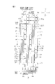
- FIG. 1 is an illustrative plan view showing an acceleration sensor according to an embodiment of the present disclosure
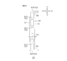
- FIG. FIG. 2 is a schematic plan view mainly showing the X-axis sensor.
- 3 is an enlarged plan view of a main part of FIG. 2.
- FIG. 4 is a schematic enlarged cross-sectional view taken along line IV-IV of FIG. 3.
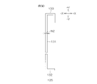
- FIG. 5A is a schematic enlarged plan view showing a spring portion used in the X-axis sensor shown in FIG. 3.
- FIG. 5B is an illustrative enlarged plan view showing a first modified example of the spring portion;
- FIG. 5C is an illustrative enlarged plan view showing a second modification of the spring portion.
- FIG. 5D is an illustrative enlarged plan view showing a spring portion used in the X-axis sensor according to the reference example shown in FIG. 6.
- FIG. FIG. 6 is an illustrative main part enlarged plan view showing a reference example of the X-axis sensor.
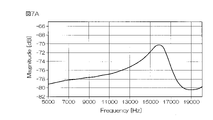
- FIG. 7A is a graph showing the relationship between vibration frequency and amplitude in the X-axis sensor of this embodiment.
- FIG. 7B is a graph showing the relationship between vibration frequency and amplitude in the X-axis sensor according to the reference example.
- FIG. 8 is a schematic plan view showing a modification of the X-axis sensor.
- FIG. 9A is an illustrative enlarged plan view showing a spring portion used in an X-axis sensor according to a modification; FIG.
- FIG. 9B is an illustrative enlarged plan view showing a reference example of the spring portion.
- FIG. 10 is a schematic plan view showing the Z-axis sensor.
- 11A is an enlarged plan view of a main part of FIG. 10.
- FIG. 11B is an enlarged plan view of a main part showing a reference example of the Z-axis sensor.
- FIG. 12 shows the positional relationship in the Z-axis direction between the fixed electrode and the movable electrode of the Z-axis sensor when acceleration in the Z-axis direction is acting, and the fixed electrode of the Z-axis sensor when acceleration in the Z-axis direction is acting. and a positional relationship in the Z-axis direction of the movable electrode.
- FIG. 10 is a schematic plan view showing the Z-axis sensor.
- 11A is an enlarged plan view of a main part of FIG. 10.
- FIG. 11B is an enlarged plan view of a main part showing a reference example of the Z-axis sensor.
- FIG. 13A is a graph showing the relationship between vibration frequency and amplitude in the Z-axis sensor of this embodiment.
- FIG. 13B is a graph showing the relationship between vibration frequency and amplitude in the Z-axis sensor according to the reference example.
- FIG. 14 is a schematic plan view showing a modification of the Z-axis sensor.
- An embodiment of the present disclosure includes a semiconductor substrate having a cavity formed therein, a fixed structure including a fixed electrode supported by the semiconductor substrate in a state floating with respect to the cavity, and a fixed structure floating with respect to the cavity.
- a movable structure including a movable electrode supported by the semiconductor substrate via an elastic structure in a state and displaced relative to the fixed electrode, the elastic structure having a first end supported by the semiconductor substrate; a second end portion connected to the movable structure; and an intermediate portion connecting the first end portion and the second end portion; and the linear portion includes a plurality of linear frames extending parallel to each other in the direction in which the linear portion extends.
- the straight portion includes a plurality of reinforcing frames installed between the plurality of straight frames included in the straight portion.
- the linear portion includes a linear frame between the linear frames such that a triangular space is repeated along the linear frame. Includes multiple stiffening frames suspended.
- the linear portion includes a first linear portion and a second linear portion extending parallel to each other, and a third linear portion connecting one ends of the first linear portion and the second linear portion. including.
- each of said first straight portion, said second straight portion and said third straight portion includes at least one reinforcing frame spanning between said plurality of straight frames included therein. including.
- the linear portion includes a linear portion parallel to the extending direction of the movable electrode.
- the fixed electrode includes a pair of fixed electrodes extending parallel to each other in a second direction orthogonal to the first direction with an interval in a predetermined first direction
- the movable electrode includes a pair of movable electrodes disposed between said pair of fixed electrodes, spaced apart in said first direction and extending parallel to each other in said second direction.
- the fixed electrode includes a plurality of fixed electrodes formed in a comb shape in plan view
- the movable electrode includes a plurality of movable electrodes formed in a comb shape in plan view. an electrode pair, wherein the plurality of movable electrode pairs are disposed in non-contacting engagement with the plurality of fixed electrodes, each movable electrode pair being aligned with the fixed electrodes on opposite sides of the movable electrode pair; and extending parallel to each other.
- the cross-sectional shape of the fixed electrode and the cross-sectional shape of the movable electrode are squares elongated in the vertical direction.
- the elastic structure includes one straight portion and a tapered portion connected to one end of the straight portion, the straight portion consisting of two parallel straight frames.
- the tapered portion is formed from two connection frames extending obliquely outward with respect to the two linear frames such that the distance between the two connecting frames gradually widens from one end of each of the two linear frames.
- the linear portion is parallel to the extending direction of the movable electrode, or is a direction along the surface of the semiconductor substrate and orthogonal to the extending direction of the movable electrode. parallel to the direction.
- the fixed electrode includes a plurality of fixed electrodes formed in a comb shape in plan view
- the movable electrode includes a plurality of movable electrodes formed in a comb shape in plan view.
- the plurality of movable electrodes are arranged in non-contacting engagement with the plurality of fixed electrodes.
- the cross-sectional shape of the fixed electrode and the cross-sectional shape of the movable electrode are squares elongated in the vertical direction.
- one of the fixed electrode and the movable electrode is arranged in a downwardly displaced state with respect to the other.
- FIG. 1 is an illustrative plan view showing an acceleration sensor according to an embodiment of the present disclosure.
- the +X direction is a predetermined direction along the surface of the semiconductor substrate 2 in plan view
- the +Y direction is a direction along the surface of the semiconductor substrate 2 in plan view and orthogonal to the +X direction
- the +Z direction is a direction along the thickness of the semiconductor substrate 2 and perpendicular to the +X direction and the +Y direction.
- the -X direction is the direction opposite to the +X direction.
- the -Y direction is the opposite direction to the +Y direction.
- the -Z direction is the direction opposite to the +Z direction.
- the +X direction and the -X direction are collectively referred to as the "X-axis direction”.
- the +Y direction and the -Y direction are collectively referred to as the "Y-axis direction”.
- the +Z direction and the ⁇ Z direction are collectively referred to as the “Z-axis direction”.
- the acceleration sensor 1 includes a semiconductor substrate 2 having a square shape in plan view, a sensor section 3 arranged in the center of the semiconductor substrate 2, and electrode pads 4 arranged on the sides of the sensor section 3 on the semiconductor substrate 2. I'm in.
- the acceleration sensor 1 is a capacitive acceleration sensor.
- the semiconductor substrate 2 has a rectangular shape having two sides parallel to the X-axis direction and two sides parallel to the Y-axis direction in plan view.
- the sensor unit 3 has an X-axis sensor 5, a Y-axis sensor 6, and a Z-axis sensor 7 as sensors for detecting acceleration acting along three orthogonal axes in a three-dimensional space.
- the X-axis sensor 5 is for detecting acceleration acting in the X-axis direction.
- the Y-axis sensor 6 is for detecting acceleration in the Y-axis direction.
- the Z-axis sensor 7 is for detecting acceleration in the Z-axis direction.
- the semiconductor substrate 2 is made of a conductive silicon substrate (for example, a low resistance substrate having a resistivity of 5 ⁇ m to 500 ⁇ m).
- the semiconductor substrate 2 has a cavity 10 (see FIG. 4) inside, and an X-axis sensor 5, an X-axis sensor 5, and an X-axis sensor 5 are mounted on an upper wall (surface layer) 11 of the semiconductor substrate 2 having a top surface that partitions the cavity 10 from the surface side.
- a Y-axis sensor 6 and a Z-axis sensor 7 are formed.
- the X-axis sensor 5, the Y-axis sensor 6, and the Z-axis sensor 7 are part of the semiconductor substrate 2, and are attached to the bottom wall 12 (see FIG. 4) of the semiconductor substrate 2 having a bottom surface that defines the cavity 10 from the back side. It is supported in a floating state.
- the X-axis sensor 5 and the Y-axis sensor 6 are arranged adjacent to each other with an interval in the X-axis direction.
- Two Z-axis sensors 7 are arranged to surround each of the X-axis sensor 5 and the Y-axis sensor 6 .
- the Y-axis sensor 6 has substantially the same configuration as the X-axis sensor 5 rotated by 90° in plan view.
- a lid 8 made of, for example, a silicon substrate and bonded to the surface of the semiconductor substrate 2 .
- the electrode pads 4 are connected to external electronic components to input signals to the sensors 5-7 and output signals from the sensors 5-7. 1) is provided.
- the external electronic component is, for example, an ASIC (Application Specific Integrated Circuit) element.
- FIG. 2 is a schematic plan view mainly showing the X-axis sensor.
- 3 is an enlarged plan view of a main part of FIG. 2.
- FIG. 4 is a schematic enlarged cross-sectional view taken along line IV-IV of FIG. 3.
- FIG. 5A is a schematic enlarged plan view showing the spring portion of FIG. 3;
- a support portion 14 is formed between the X-axis sensor 5 and the Z-axis sensor 7 to support the X-axis sensor 5 in a floating state.
- the support portion 14 includes a support base portion 16 extending across the Z-axis sensor 7 toward the X-axis sensor 5 from the upper portion of one side wall 15 having a side surface that laterally partitions the cavity 10 of the semiconductor substrate 2; An annular portion 17 surrounding the sensor 5 is integrally included.
- the supporting portion 14 is supported by one side wall 15 of the semiconductor substrate 2 while floating from the bottom wall 12 of the semiconductor substrate 2 .
- the support base portion 16 has a rectangular shape elongated in the Y-axis direction in a plan view.
- the annular portion 17 has a rectangular annular shape in plan view, and includes a first frame portion 17A on the ⁇ Y side, a second frame portion 17B on the ⁇ X side, a third frame portion 17C on the +Y side, and a fourth frame portion 17D on the +X side. including.
- the first frame portion 17A is divided at the length center portion.
- a length center portion of the second frame portion 17B is connected to the support base portion 16 .
- the X-axis sensor 5 is arranged inside the annular portion 17 and supported by the annular portion 17 .
- the X-axis sensor 5 has a fixed structure 21 fixed to the support portion 14 provided in the cavity 10 and a movable structure 22 held vibratably with respect to the fixed structure 21 .
- the fixed structure 21 and the movable structure 22 are formed with the same thickness.
- the fixed structure 21 includes a fixed base portion 23 and a plurality of fixed electrodes 24 .
- the fixed base portion 23 extends in the X-axis direction along the inner wall of the first frame portion 17A and is fixed to the support portion 14 .
- the fixed base portion 23 has a ladder-like frame structure in a plan view, including a plurality of (two in this embodiment) main frames extending parallel to each other and a plurality of sub-frames installed between the plurality of main frames. doing.
- a plurality of fixed electrodes 24 are formed in a comb shape on the inner wall of the fixed base portion 23 .
- the plurality of fixed electrodes 24 are arranged parallel to each other at regular intervals in the X-axis direction. That is, the fixed electrodes 24 extend in the +Y direction from the fixed base portion 23 .
- the movable structure 22 includes a movable base portion 26 and a plurality of movable electrode portions 27 .
- the movable base portion 26 extends in the X-axis direction along the inner wall of the third frame portion 17C. Both ends of the movable base portion 26 are connected to the fixed base portion 23 via spring portions 25 that are extendable along the X-axis direction.
- the spring portion 25 is an example of the "elastic structure" of the present invention.
- the movable base portion 26 includes a plurality of (five in this embodiment) main frames 26A extending parallel to the X-axis direction, and a plurality of sub-frames 26B installed between the plurality of main frames 26A. It has a shaped frame structure.
- a plurality of movable electrode portions 27 are formed in a comb shape on the inner wall of the movable base portion 26 .
- the plurality of movable electrode portions 27 are arranged parallel to each other at equal intervals in the X-axis direction.
- a plurality of movable electrode portions 27 extend from the movable base portion 26 toward between the fixed electrodes 24 adjacent to each other. That is, the comb tooth-shaped movable electrode portion 27 is arranged so as to mesh with the comb tooth-shaped fixed electrode 24 without coming into contact with the fixed electrode 24 .
- Each movable electrode portion 27 includes a first movable electrode 27A and a second movable electrode 27B extending parallel to each other in the ⁇ Y direction from the ⁇ Y side ends of a pair of adjacent sub-frames 26B in the movable base portion 26, and and a plurality of connecting portions 27C that connect the .
- a length intermediate portion of each connecting portion 27C is constituted by a first isolated coupling portion (insulating layer) 91 made of silicon oxide (SiO 2 ).
- the first movable electrode 27A and the second movable electrode 27B are electrically insulated.
- the first movable electrode 27A and the second movable electrode 27B included in the movable electrode portion 27 are examples of the "movable electrode pair" of the present invention.
- the cross-sectional shape of the fixed electrode 24 and the movable electrodes 27A and 27B is, as shown in FIG. 4, a rectangular shape elongated in the Z-axis direction.
- the fixed electrode 24 and the movable electrodes 27A and 27B are plate-shaped with the thickness direction being the X-axis direction.
- first movable subframe 26Ba the subframe to which the first movable electrode 27A is connected
- second movable subframe 26Bb the subframe to which the second movable electrode 27B is connected
- a second isolating joint (insulating layer) 92 made of silicon oxide is formed in the main frame 26A at the intermediate length of the portion connecting two adjacent sub-frames 26B. Therefore, each subframe 26B is electrically isolated from other subframes 26B.
- Each movable electrode 27A, 27B is electrically insulated from the other movable electrodes 27A, 27B by the first isolation joint 91 and the second isolation joint 92 .
- the first movable electrode 27A is arranged on the -X side with respect to the second movable electrode 27B.
- the distance between the first movable electrode 27A and the fixed electrode 24 adjacent thereto is equal to the distance between the second movable electrode 27B and the fixed electrode 24 adjacent thereto.
- the -Y side ends of the spring portion 25 arranged on the -X side and the spring portion 25 arranged on the +Y side are constituted by a third isolation coupling portion (insulating layer) 93 made of silicon oxide in the middle of the length. It is mechanically connected to the fixed base portion 23 via the connecting frame. Therefore, the fixed base portion 23 and the spring portion 25 are electrically insulated.
- the +Y side end of the spring portion 25 arranged on the -X side is mechanically and electrically connected to the first movable sub-frame 26Ba on the most -X side.
- the +Y side end of the spring portion 25 arranged on the +X side is mechanically and electrically connected to the second movable sub-frame 26Bb on the most +X side.
- These spring portions 25 function as springs that support the movable base portion 26 so as to be movable in the X-axis direction, and also function as conductive paths.
- An insulating film (not shown) is formed on the surface of the semiconductor substrate 2 including the fixed structure 21 and the movable structure 22 .
- a plurality of wirings (not shown) are formed on the surface of the insulating film.
- the plurality of wirings are the first wiring for electrically connecting the plurality of fixed electrodes 24 to the electrode pad 4 for the fixed electrode, and the plurality of first movable electrodes 27A for electrically connecting the electrode pad 4 for the first movable electrode. and a third wiring for electrically connecting the plurality of second movable electrodes 27B to the electrode pads 4 for the second movable electrodes.
- the second wiring is wiring for electrically connecting the plurality of first movable sub-frames 26Ba to each other and wiring for electrically connecting the -X side spring portion 25 to the electrode pad 4 for the first movable electrode.
- the third wiring includes wiring for electrically connecting the plurality of second movable sub-frames 26Bb to each other and wiring for electrically connecting the spring portion 25 on the +X side to the electrode pad 4 for the second movable electrode.
- the lengths of the X-axis sensor 5 in the X-axis direction and the Y-axis direction are, for example, about 300 ⁇ m.
- the length in the Z-axis direction from the +Z-side surface of the X-axis sensor 5 to the inner surface (+Z-side surface) of the bottom wall 12 (see FIG. 4) of the semiconductor substrate 2 is, for example, about 50 ⁇ m.
- the length in the Z-axis direction from the +Z-side surface of the X-axis sensor 5 to the outer surface (-Z-side surface) of the bottom wall 12 of the semiconductor substrate 2 is, for example, about 200 ⁇ m to 300 ⁇ m.
- the lengths of the fixed electrode 24, the first movable electrode 27A and the second movable electrode 27B in the Z-axis direction are, for example, about 15 ⁇ m to 30 ⁇ m.
- the movable base portion 26 supported by the two spring portions 25 vibrates in the X-axis direction.
- the first movable electrode 27A and the second movable electrode 27B extending from the movable base portion 26 also vibrate in the X-axis direction between the two fixed electrodes 24 adjacent to each other.
- the movable base portion 26 moves in the +X direction
- the first movable electrode 27A moves away from the adjacent fixed electrode 24, and the second movable electrode 27B moves closer to the adjacent fixed electrode 24.
- the first movable electrode 27A moves closer to the adjacent fixed electrode 24, and the second movable electrode 27B moves away from the adjacent fixed electrode 24.
- the facing distance d1 between the first movable electrode 27A and the fixed electrode 24 adjacent thereto and the facing distance d2 between the second movable electrode 27B and the fixed electrode 24 adjacent thereto change.
- a change in capacitance C1 between the first movable electrode 27A/fixed electrode 24 due to a change in the facing distance d1 and a change in capacitance C1 between the second movable electrode 27B/fixed electrode 24 due to a change in the facing distance d2 Acceleration in the X-axis direction is detected by detecting a change in C2.
- the -X side spring portion 25 is composed of a straight portion 30 extending in the Y-axis direction.
- the straight portion 30 includes two straight frames 31 extending in parallel in the Y-axis direction and a plurality of reinforcing frames 32 installed between the straight frames 31 .
- a first connecting portion 33 extending in the +X direction is connected to the +X side end of the first reinforcing frame 32A.
- a second connecting portion 34 extending in the +X direction is connected to the +X side end of the second reinforcing frame 32B.
- the ⁇ Y side end of the spring portion 25 (linear portion 30 ) is mechanically connected to the fixed base portion 23 via the first connection portion 33 .
- the +Y side end of the spring portion 25 (linear portion 30) is mechanically and electrically connected to the first movable sub-frame 26Ba via the second connection portion .
- the spring portion 25 arranged on the +X side is located at the -X side spring portion 25 with respect to a straight line passing through the center between the -X side spring portion 25 and the +X side spring portion 25 and extending in the Y-axis direction. It has a planar shape that is symmetrical with Therefore, in the +X side spring portion 25, the first connecting portion 33 extending in the -X direction is connected to the -X side end of the first reinforcing frame 32A, and the -X side end of the second reinforcing frame 32B is connected to A second connecting portion 34 extending in the -X direction is connected.
- the ⁇ Y side end of the +X side spring portion 25 (linear portion 30 ) is mechanically connected to the fixed base portion 23 via the first connection portion 33 .
- the +Y side end of the +X side spring portion 25 (linear portion 30) is mechanically and electrically connected to the second movable sub-frame 26Bb via the second connection portion .
- FIG. 6 is an illustrative main part enlarged plan view showing a reference example of the X-axis sensor.
- the same reference numerals as in FIG. 3 denote the parts corresponding to the parts in FIG. 3 described above.
- 5D is an illustrative enlarged plan view showing a spring portion used in the X-axis sensor according to the reference example shown in FIG. 6.
- the -X side spring portion 125 used in the X-axis sensor 105 is composed of a linear portion 131 made up of a single linear frame extending in the Y-axis direction.
- a first connecting portion 132 extending in the +X direction from the -Y direction end of the straight portion 131 is connected to the -Y direction end of the straight portion 131 .
- the +Y direction end of the straight portion 131 is connected to a hook-shaped second connection portion 133 extending in the -Y direction after extending in the +X direction from the +Y direction end of the straight portion 131 .
- the ⁇ Y side end of the spring portion 125 (linear portion 131 ) is mechanically connected to the fixed base portion 23 via the first connection portion 132 .
- the +Y side end of the spring portion 125 (linear portion 131) is mechanically and electrically connected to the second movable sub-frame 26Bb via the second connection portion 133. As shown in FIG.
- the spring portion 125 arranged on the +X side is located on the -X side with respect to a straight line passing through the center between the -X side spring portion 125 and the -X side spring portion 125 and extending in the Y-axis direction. 125 and has a plane shape of line symmetry.
- a first connection portion 132 extending in the -X direction is connected to the -Y side end of a straight portion 131 made of one straight frame, and the +Y side end of the straight portion 131 is connected to the -Y side end.
- a hook-shaped second connecting portion 133 extending in the -Y direction is connected.
- the ⁇ Y side end of the +X side spring portion 125 (linear portion 131 ) is mechanically connected to the fixed base portion 23 via the first connection portion 132 .
- the +Y side end of the +X side spring portion 125 (linear portion 131) is mechanically and electrically connected to the first movable sub-frame 26Ba via a second connection portion 133. As shown in FIG.
- the width of the linear portion 30 can be made larger than in the spring portion 125 of the X-axis sensor 105 according to the reference example. That is, the width W1 (see FIG. 5A) of the linear portion 30 of the spring portion 25 can be made larger than the width W2 (see FIG. 5D) of the linear portion 131 of the spring portion 125. As shown in FIG. Thereby, the resonance frequency of the movable portion of the X-axis sensor 5 can be increased. This makes it possible to widen the range of detectable acceleration.
- FIG. 7A is a graph showing the relationship between vibration frequency and amplitude in the X-axis sensor 5 of this embodiment.
- FIG. 7B is a graph showing the relationship between vibration frequency and amplitude in the X-axis sensor 105 according to the reference example.
- the X-axis sensor 5 of this embodiment can increase the resonance frequency of the movable portion compared to the X-axis sensor 105 according to the reference example.
- FIG. 5B is an illustrative plan view showing a first modification of the spring portion arranged on the -X side.
- the ⁇ X side spring portion 25A shown in FIG. 5B consists of a linear portion 30A extending parallel to the Y-axis direction.
- the linear portion 30A includes two linear frames 31 extending parallel to the Y-axis direction, a first reinforcing frame 32A connecting the -Y side ends of the linear frames 31, and the +Y side ends of the linear frames 31. and a second reinforcing frame 32B.
- the straight portion 30A includes a third reinforcing frame 32D that reinforces the straight frames 31 so that triangular spaces are repeated along the straight frames 31 between the two straight frames 31. As shown in FIG.
- a first connecting portion 33 extending in the +X direction is connected to the +X side end of the first reinforcing frame 32A.
- a second connecting portion 34 extending in the +X direction is connected to the +X side end of the second reinforcing frame 32B.
- the ⁇ Y side end of the spring portion 25A (linear portion 30A) is mechanically connected to the fixed base portion 23 via the first connection portion 33 .
- the +Y side end of the spring portion 25A (linear portion 30A) is mechanically and electrically connected to the first movable sub-frame 26Ba via the second connection portion .
- the spring portion 25A arranged on the +X side is the -X side spring with respect to a straight line extending in the Y-axis direction passing through the center between the -X side spring portion 25A and the +X side spring portion 25A. It has a planar shape line-symmetrical to the portion 25A. Therefore, in the +X side spring portion 25A, the first connection portion 33 extending in the -X direction is connected to the -X side end of the first reinforcing frame 32A, and the -X side end of the second reinforcing frame 32B The second connecting portion 34 extending in the -X direction is connected.
- the ⁇ Y side end of the +X side spring portion 25A (linear portion 30A) is mechanically connected to the fixed base portion 23 via the first connection portion 33 .
- the +Y side end of the +X side spring portion 25A (linear portion 30A) is mechanically and electrically connected to the second movable sub-frame 26Bb via the second connection portion 34 .
- FIG. 5C is an illustrative plan view showing a second modification of the spring portion arranged on the -X side.
- the ⁇ X side spring portion 25B shown in FIG. 5C consists of a straight portion 30B extending parallel to the Y-axis direction.
- the straight portion 30B includes three straight frames 31 extending in parallel in the Y-axis direction and a plurality of reinforcing frames 32 installed between the straight frames 31 .
- the reinforcing frames 32 include a first reinforcing frame 32A connecting the ends of the three linear frames 31 in the -Y direction, and a second reinforcing frame 32B connecting the ends of the three linear frames 31 in the +Y direction. and a plurality of third reinforcing frames 32C that connect the lengthwise intermediate portions of the straight frames 31 to each other.
- a first connecting portion 33 extending in the +X direction is connected to the +X side end of the first reinforcing frame 32A.
- a second connecting portion 34 extending in the +X direction is connected to the +X side end of the second reinforcing frame 32B.
- the ⁇ Y side end of the spring portion 25B (straight portion 30B) is mechanically connected to the fixed base portion 23 via the first connection portion 33 .
- the +Y side end of the spring portion 25B (linear portion 30B) is mechanically and electrically connected to the first movable sub-frame 26Ba via the second connection portion .
- the spring portion 25B arranged on the +X side is arranged on the -X side with respect to a straight line passing through the center between the -X side spring portion 25B and the +X side spring portion 25B and extending in the Y-axis direction. It has a planar shape that is symmetrical with Therefore, in the +X side spring portion 25B, the first connecting portion 33 extending in the -X direction is connected to the -X side end of the first reinforcing frame 32A, and the -X side end of the second reinforcing frame 32B The second connecting portion 34 extending in the -X direction is connected.
- the ⁇ Y side end of the +X side spring portion 25B (linear portion 30B) is mechanically connected to the fixed base portion 23 via the first connection portion 33 .
- the +Y side end of the +X side spring portion 25B (linear portion 30B) is mechanically and electrically connected to the second movable sub-frame 26Bb via the second connection portion 34 .
- Y-axis sensor 6 has substantially the same configuration as the X-axis sensor 5 rotated by 90° in plan view, so detailed description thereof will be omitted.
- the fixed electrode 24, the first movable electrode 27A, and the second movable electrode 27B each extend in the X-axis direction. vibrate in one direction.
- the first movable electrode 27A and the second movable electrode 27B also vibrate in the Y-axis direction between the two fixed electrodes 24 adjacent to each other.
- FIG. 8 is a schematic plan view showing a modification of the X-axis sensor.
- the X-axis sensor 5A has a fixed structure 21 fixed to the semiconductor substrate 2 and a movable structure 22 held vibratably with respect to the fixed structure 21 .
- the fixed structure 21 and the movable structure 22 are formed with the same thickness.
- the fixed structure 21 and the movable structure 22 are supported by the semiconductor substrate 2 while floating from the bottom wall of the semiconductor substrate 2 .
- the fixed structure 21 includes a fixed base portion 23 and a plurality of fixed electrodes 24 .
- the fixed base portion 23 has a quadrangular annular shape in a plan view, and is arranged so as to surround the periphery of the arrangement area of the X-axis sensor 5A.
- the fixed base portion 23 includes a -Y side first frame portion 23A, a -X side second frame portion 23B, a +Y side third frame portion 23C, and a -X side fourth frame portion 23D.
- a length center portion of the second frame portion 23B and a length center portion of the fourth frame portion 23D are supported by the semiconductor substrate 2 .
- Each of the frame portions 23A to 23D of the fixed base portion 23 includes a plurality of (two in the example of FIG. 8) main frames extending parallel to each other, and a plurality of sub-frames bridged between the plurality of main frames in plan view. It has a ladder-like frame structure.
- the plurality of fixed electrodes 24 includes a plurality of first fixed electrodes 24A formed in a comb-like shape on the inner wall of the first frame portion 23A, and a plurality of comb-like fixed electrodes 24A formed in a comb-like shape on the inner wall of the third frame portion 23C. and a second fixed electrode 24B.
- the plurality of first fixed electrodes 24A extend from the first frame portion 23A to the vicinity of the central portion in the Y-axis direction of the arrangement area of the X-axis sensor 5A.
- the plurality of second fixed electrodes 24B extend from the third frame portion 23C to the vicinity of the central portion in the Y-axis direction of the arrangement area of the X-axis sensor 5A.
- the plurality of first fixed electrodes 24A extend parallel to each other in the +Y direction from the first frame portion 23A at equal intervals in the X-axis direction.
- the plurality of second fixed electrodes 24B extend parallel to each other in the -Y direction from the third frame portion 23C at equal intervals in the X-axis direction.
- the movable structure 22 includes a movable base portion 26 and a plurality of movable electrode portions 27 .
- the movable base portion 26 extends in the X-axis direction at the central portion in the Y-axis direction of the arrangement area of the X-axis sensor 5A, and both ends of the movable base portion 26 are fixed to the fixed base portion 23 via spring portions 28 that are elastic in the X-axis direction. It is
- the spring portion 28 is an example of the "elastic structure" of the present invention.
- the movable base portion 26 consists of a plurality of (four in this embodiment) frames extending parallel to the X-axis direction, and both ends thereof are connected to the spring portions 28 .
- Two spring portions 28 are provided at each end of the movable base portion 26 .
- a plurality of movable electrode portions 27 are formed in a comb shape on each side wall of the movable base portion 26 .
- the plurality of movable electrode portions 27 extend across the movable base portion 26 toward between the first fixed electrodes 24A adjacent to each other and between the second fixed electrodes 24B adjacent to each other.
- the comb tooth-shaped movable electrode portion 27 extending from the movable base portion 26 to the -Y side is arranged so as to mesh with the first comb tooth-shaped fixed electrode 24A without coming into contact with the first fixed electrode 24A.
- the comb-teeth-shaped movable electrode portion 27 extending from the movable base portion 26 toward the +Y side is arranged so as to mesh with the comb-teeth-shaped second fixed electrode 24B without contacting the second fixed electrode 24B.
- Each movable electrode portion 27 includes a first movable electrode 27A and a second movable electrode 27B extending parallel to each other in the Y-axis direction at intervals in the X-axis direction, and a plurality of connecting portions 27C connecting them.
- a lengthwise intermediate portion of each connecting portion 27C is constituted by an isolated joint portion (not shown) made of silicon oxide.
- the first movable electrode 27A and the second movable electrode 27B included in the movable electrode portion 27 are examples of the "movable electrode pair" of the present invention.
- the first movable electrode 27A is arranged on the -X side with respect to the second movable electrode 27B.
- the distance between the first movable electrode 27A and the adjacent first fixed electrode 24A or the second fixed electrode 24B is the distance between the second movable electrode 27B and the adjacent second movable electrode 27B. It is equal to the distance between the first fixed electrode 24A and the second fixed electrode 24B.
- Each first movable electrode 27A is electrically insulated from the other first movable electrodes 27A and second movable electrodes 27B at the movable base portion 26.
- Each second movable electrode 27B is electrically insulated from the other second movable electrodes 27B and the first movable electrodes 27A at the movable base portion 26 .
- the two spring portions 28 arranged on the -X side are connected to the first movable electrode 27A arranged on the most -X side in the movable base portion 26 .
- the two spring portions 28 arranged on the +X side are connected to the second movable electrode 27B arranged on the most +X side in the movable base portion 26 .
- the four spring portions 28 function as springs that support the movable base portion 26 so as to be movable in the X-axis direction, and also function as conductive paths.
- An insulating film (not shown) is formed on the surface of the semiconductor substrate 2 including the fixed structure 21 and the movable structure 22 .
- a wiring (not shown) is formed on the surface of the insulating film.
- the wires are first wires for electrically connecting the plurality of first fixed electrodes 24A and the plurality of second fixed electrodes 24B to the electrode pads 4 for fixed electrodes, and the plurality of first movable electrodes 27A are connected to the first movable electrodes 27A. and a third wiring for electrically connecting the plurality of second movable electrodes 27B to the electrode pad 4 for the second movable electrode.
- the movable base portion 26 supported by the four spring portions 28 vibrates in the X-axis direction.
- the first movable electrode 27A and the second movable electrode 27B extending from the movable base portion 26 are also arranged between two adjacent first fixed electrodes 24A and between two adjacent second fixed electrodes 24B. Vibrate axially.
- FIG. 9A is a schematic plan view showing the spring portion 28 arranged on the +Y side on the -X side.
- the spring portion 28 has a vertically elongated U shape opening downward in plan view. Specifically, the spring portion 28 is arranged on the +X side of the first linear portion 28B and the first linear portion 28B extending in the Y-axis direction in plan view, and parallel to the first linear portion 28B. and a third straight portion (connecting portion) 28C that connects the +Y direction ends of the first straight portion 28B and the second straight portion 28D.
- the spring portion 28 further includes a first connecting portion 28A extending in the -X direction from the -Y side end of the first straight portion 28B and a second connecting portion 28A extending in the +X direction from the -Y side end of the second straight portion 8D. and part 28E.
- the first connection portion 28A, the first straight portion 28B, the third connection portion 28C, the second straight portion 28D and the second connection portion 28E each include two straight frames 35 extending parallel to each other.
- the first linear portion 28B, the third connecting portion 28C and the second linear portion 28D include one or more reinforcing frames 36 installed between the linear frames 35. As shown in FIG.
- a first end of the spring portion 28 (-Y side end of the first linear portion 28B) is mechanically connected to the second frame portion 23B of the fixed base portion 23 via a first connection portion 28A.
- the second end of the spring portion 28 (-Y side end of the second linear portion 28D) is mechanically and electrically connected to the movable base portion 26 via the second connection portion 28E.
- the spring portion 28 arranged on the -Y side on the -X side passes through the center between the +Y side spring portion 28 on the -X side and the -Y side spring portion 28 on the -X side and extends in the X-axis direction. It has a plane shape symmetrical to the spring portion 28 on the +Y side on the -X side with respect to the extending straight line.
- a first end of the spring portion 28 (+Y side end of the first linear portion 28B) is mechanically connected to the second frame portion 23B of the fixed base portion 23 via a first connection portion 28A. .
- the second end of the spring portion 28 (+Y side end of the second linear portion 28D) is mechanically and electrically connected to the movable base portion 26 via the second connection portion 28E.
- the two spring portions 28 on the +X side are located on the -X side with respect to a straight line passing through the center between the two spring portions 28 on the -X side and the two spring portions 28 on the +X side and extending in the Y-axis direction. It has a planar shape line-symmetrical to the two spring portions 28 .
- FIG. 9B is an illustrative plan view showing a reference example of the spring portion arranged on the +Y side on the -X side.
- the overall shape of the spring portion 128 of the reference example is the same as the spring portion 28 of FIG. It consists of two straight portions 128D and a second connecting portion 128E. However, in the spring portion 128 of the reference example, each of these portions 128A to 128E is composed of one linear frame 135 respectively.
- the widths of the linear portions 28B to 28D can be increased compared to the spring portion 128 of the reference example. That is, the width of the linear portions 28B-28D of the spring portion 28 can be made larger than the width of the linear portions 128B-128D of the spring portion 128.
- the resonance frequency of the movable portion can be increased compared to the X-axis sensor using the spring portion 128 of the reference example. This makes it possible to widen the range of detectable acceleration.
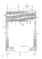
- FIG. 10 is a schematic plan view showing the Z-axis sensor.
- 11A is an enlarged plan view of a main part of FIG. 10.
- FIG. 10 is a schematic plan view showing the Z-axis sensor.
- the semiconductor substrate 2 has the cavity 10 (see FIG. 4) inside, as described above.
- a supporting portion 14 supports the X-axis sensor 5 and the Y-axis sensor 6 in a floating state with respect to the bottom wall 12 (see FIG. 4) of the semiconductor substrate 2 so as to surround each of them.
- a Z-axis sensor 7 is arranged.
- the Z-axis sensor 7 has a fixed structure 51 fixed to the support portion 14 (support base portion 16) provided in the cavity 10, and a movable structure 52 held vibratably with respect to the fixed structure 51. ing.
- the fixed structure 51 and the movable structure 52 are formed with the same thickness.
- the fixing structure 51 is arranged so as to surround the X-axis sensor 5 (more specifically, the annular portion 17 of the supporting portion 14 described above).
- a movable structure 52 is arranged so as to further surround it.
- the fixed structure 51 and the movable structure 52 are integrally connected to the side wall on the ⁇ Y side and the side wall on the +Y side of the supporting base portion 16 .
- the Z-axis sensor 7 arranged to surround the Y-axis sensor 6 is arranged so that the movable structure 52 surrounds the Y-axis sensor 6 (not shown).
- a fixed structure 51 is arranged.
- the fixed structure 51 includes a fixed base portion 53 having a quadrangular annular shape in a plan view and fixed to the support base portion 16 .
- the fixed base portion 53 includes a ⁇ Y side frame portion, a ⁇ X side frame portion, a +Y side frame portion, and a +X side frame portion.
- the fixed structure 51 further includes a fixed electrode structure provided on the +X side frame portion of the fixed base portion 53 .
- Each frame portion of the fixed base portion 53 has a ladder-like frame structure in a plan view including a plurality of linear main frames extending parallel to each other and a plurality of sub-frames installed between the plurality of main frames. ing.
- the fixed electrode structure includes multiple fixed backbones 55 and multiple fixed electrodes 56 .
- a plurality of fixed core portions 55 are arranged in a comb shape on the outer wall of the +X side frame portion of the fixed base portion 53 .
- the plurality of fixed core portions 55 extend parallel to each other in the +X direction from the +X side frame portion of the fixed base portion 53 at equal intervals in the Y-axis direction.
- a plurality of fixed electrodes 56 are formed in a comb shape on both side walls of each fixed base portion 55 .
- the comb-shaped fixed electrodes 56 extend parallel to each other in the Y-axis direction from both side walls of the fixed base portion 55 at equal intervals in the X-axis direction.
- the movable structure 52 includes a movable base portion 57 having a quadrangular annular shape in plan view.
- the movable base portion 57 includes a ⁇ Y side frame portion ( ⁇ Y side straight portion), a ⁇ X side frame portion ( ⁇ X side straight portion), a +Y side frame portion (+Y side straight portion), and a +X side frame portion. part (+X side straight part).
- the ⁇ X side frame portion ( ⁇ X side linear portion) of the movable base portion 57 is connected to the ⁇ X side frame portion of the fixed base portion 53, the ⁇ X side frame portion of the movable base portion 57
- the portion ( ⁇ X side linear portion) can also be regarded as part of the fixed base portion 53 .
- the movable base portion 57 is composed of the -Y side straight portion, the +Y side straight portion, and the +X side straight portion connecting the +X side ends thereof.
- the movable structure 52 further includes a +X side frame portion (+X side linear portion) of the movable base portion 57, a +X side end portion of the ⁇ Y side frame portion ( ⁇ Y side linear portion), and a +Y side frame portion (+Y side linear portion ) and a movable electrode structure formed on the +X side end of the .
- the movable electrode structure includes multiple movable backbones 59 and multiple movable electrodes 60 .
- a plurality of movable core portions 59 are formed in a comb shape on the inner wall of the +X side frame portion of the movable base portion 57 .
- a plurality of movable core portions 59 extend from the +X side frame portion of the movable base portion 57 toward between the fixed core portions 55 adjacent to each other.
- the comb tooth-shaped movable trunk portion 59 is arranged so as to mesh with the comb tooth-shaped fixed trunk portion 55 without coming into contact with the fixed trunk portion 55 .
- the plurality of movable electrodes 60 are formed in a comb-like shape on the inner wall of the -Y side frame portion of the movable base portion 57 and the plurality of first movable electrodes 60A formed in a comb-like shape on both side walls of the movable base portion 59. and a third movable electrode 60C formed in a comb shape on the inner wall of the +Y side frame portion of the movable base portion 57 .
- the plurality of first movable electrodes 60A extend from both side walls of the movable core 59 toward between the fixed electrodes 56 adjacent to each other.
- the plurality of second movable electrodes 60B extend from the -Y side frame portion of the movable base portion 57 toward between the fixed electrodes 56 adjacent to each other.
- the plurality of third movable electrodes 60C extend from the +Y side frame portion of the movable base portion 57 toward between the fixed electrodes 56 adjacent to each other.
- the plurality of movable electrodes 60 extend in the Y-axis direction.
- the comb-teeth-shaped movable electrode 60 is arranged so as to mesh with the comb-teeth-shaped fixed electrode 56 without coming into contact with the fixed electrode 24 .
- Each frame portion of the movable base portion 57 has a ladder-like frame structure in a plan view including a plurality of linear main frames extending parallel to each other and a plurality of sub-frames installed between the plurality of main frames. ing.
- the -Y side end portion of the -X side frame portion of the movable base portion 57 and the -X side end portion of the -Y side frame portion of the movable base portion 57 are connected via the -Y side spring portion 61.
- the +Y side end of the ⁇ X side frame portion of the movable base portion 57 and the ⁇ X side end portion of the +Y side frame portion of the movable base portion 57 are connected via the +Y side spring portion 61 .
- the spring portion 61 is an example of the "elastic structure" of the present invention.
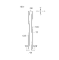
- the +Y side spring portion 61 is composed of a linear portion 61A extending in the Y-axis direction and a tapered portion 61B formed at the -Y side end of the linear portion 61A.
- the straight portion 61A consists of two straight frames 62 extending parallel to each other in the Y-axis direction.
- the tapered portion 61B is composed of two inclined frames 63 extending obliquely outward from the two linear frames 62 from the -Y side ends of the two linear frames 62 so that the distance between them gradually widens. .
- the first end of the spring portion 61 (the -Y side end of the tapered portion 61B) is supported by the support base portion 16 via the -X side frame portion of the movable base portion 57. As shown in FIG.
- the second end of the spring portion 61 (the +Y side end of the straight portion 61A) is mechanically and electrically connected to the ⁇ X side end of the +Y side frame portion of the movable base portion 57 .
- the ⁇ Y side spring portion 61 is symmetrical with the +Y side spring portion 61 with respect to a straight line passing through the center between the +Y side spring portion 61 and the ⁇ Y side spring portion 61 and extending in the X-axis direction. It has a planar shape of The ⁇ Y side spring portion 61 is composed of a linear portion 61A extending in the Y-axis direction and a tapered portion 61B formed at the +Y side end of the linear portion 61A.
- the straight portion 61A consists of two straight frames 62 extending parallel to each other in the Y-axis direction.
- the tapered portion 61B is composed of two inclined frames 63 extending obliquely outward from the two linear frames 62 from the +Y side ends of the two linear frames 62 so that the distance between them gradually widens.
- the first end of the -Y side spring portion 61 (the +Y side end of the tapered portion 61B) is supported by the support base portion 16 via the -X side frame portion of the movable base portion 57 .
- the second end of the -Y side spring portion 61 (the -Y side end of the linear portion 61A) is mechanically and electrically connected to the -X side end of the -Y side frame portion of the movable base portion 57.
- the two spring portions 61 function as springs for making the movable electrode 60 movable in the Z-axis direction.
- the spring portion 61 is elastically distorted, and the movable base portion 57 is moved as if it were a pendulum, with the spring portion 61 as a fulcrum, and the bottom wall 12 of the semiconductor substrate 2 (see FIG. 4).
- the movable electrode 60 meshing with the fixed electrode 56 in a comb-teeth shape vibrates in the Z-axis direction.
- the movable electrode 60 vibrates in the Z-axis direction.
- the area of the overlapping region of the facing surfaces of the movable electrode 60 and the fixed electrode 56 changes. Acceleration acting in the Z-axis direction can be detected by electrically detecting a change in capacitance due to a change in the area.
- the Z-axis sensor 7 arranged to surround the X-axis sensor 5 will be referred to as the "first Z-axis sensor 7A”
- the Z-axis sensor 7 arranged to surround the Y-axis sensor 6 will be referred to as the "second Z-axis sensor 7A”.
- sensor 7B the Z-axis sensor 7 arranged to surround the X-axis sensor 5
- the fixed structure 51 arranged inside the movable structure 52 is affected by the silicon oxide film (not shown) formed on the surface of the fixed base portion 53, and the fixed electrode structure is It is warped so that it hangs down on the -Z side.
- the movable structure 52 arranged inside the fixed structure 51 is affected by the silicon oxide film (not shown) formed on the surface of the movable base portion, and the movable electrode structure is shifted to the -Z side. It is warped as if it were hanging down.
- FIG. 12 shows the positional relationship in the Z-axis direction between the fixed electrode and the movable electrode of the Z-axis sensor when acceleration in the Z-axis direction does not act, and the fixed electrode of the Z-axis sensor when acceleration in the Z-axis direction acts. and a positional relationship in the Z-axis direction of the movable electrode.
- F denotes the fixed electrode
- M denotes the movable electrode.
- FIG. 12 shows the positional relationship in the Z-axis direction between the fixed electrode F and the movable electrode M when no acceleration in the Z-axis direction acts on the acceleration sensor 1 in the first Z-axis sensor 7A. .
- FIG. 12 shows the positional relationship in the Z-axis direction between the fixed electrode F and the movable electrode M when no acceleration in the Z-axis direction acts on the acceleration sensor 1 in the second Z-axis sensor 7B. .
- FIG. 12 shows the positional relationship in the Z-axis direction between the fixed electrode F and the movable electrode M of the first Z-axis sensor 7A when acceleration in the +Z direction acts on the acceleration sensor 1 .
- the lower right of FIG. 12 shows the positional relationship in the Z-axis direction between the fixed electrode F and the movable electrode M of the second Z-axis sensor 7B when +Z-direction acceleration acts on the acceleration sensor 1 .
- the fixed electrode F is arranged at a position shifted to the -Z side with respect to the movable electrode M.
- the movable electrode M is arranged at a position shifted to the -Z side with respect to the fixed electrode F.
- the movable electrode M moves in the -Z direction with respect to the fixed electrode F, as shown in FIG.
- the capacitance C1 between the fixed electrode F and the movable electrode M increases in the first Z-axis sensor 7A
- the capacitance C2 between the fixed electrode F and the movable electrode M increases in the second Z-axis sensor 7B. Decrease.
- the Z Axial acceleration is detected.
- FIG. 11B is an enlarged plan view of a main part showing a reference example of the Z-axis sensor.
- the same reference numerals as those of FIG. 11A are used for the portions corresponding to the respective portions of FIG. 11A described above.
- the Z-axis sensor 107 shown in FIG. 11B has a structure similar to that of the Z-axis sensor 7 described above, but differs from the Z-axis sensor 7 described above in the structure of the spring portion and its vicinity.
- the ⁇ X side frame portion of the movable base portion 57 is composed of one main frame.
- the +Y side end portion of the ⁇ X side frame portion of the movable base portion 57 is connected to the +Y side frame portion of the movable base portion 57 via the +Y side spring portion 161
- the ⁇ X side frame portion of the movable base portion 57 is connected to the +Y side frame portion of the movable base portion 57 via the spring portion 161 on the +Y side.
- the ⁇ Y side end portion is connected to the ⁇ Y side frame portion of the movable base portion 57 via a ⁇ Y side spring portion 161 having the same configuration as the spring portion 161 .
- the spring portion 161 on the +Y side is composed of a linear portion 162 consisting of a single linear frame extending in the Y-axis direction.
- a first end portion of the spring portion 161 (the ⁇ Y side end portion of the straight portion 162 ) is supported by the support base portion 16 via the ⁇ X side frame portion of the movable base portion 57 .
- a second end of the spring portion 161 (the +Y side end of the linear portion 162 ) is mechanically and electrically connected to the +Y side frame portion of the movable base portion 57 .
- the ⁇ Y side spring portion 161 is symmetrical with the +Y side spring portion 161 with respect to a straight line passing through the center between the +Y side spring portion 161 and the ⁇ Y side spring portion 161 and extending in the X-axis direction. It has a planar shape of The ⁇ Y side spring portion 161 is composed of a linear portion 162 formed of one linear frame extending in the Y-axis direction. A first end of the -Y side spring portion 161 (the +Y side end of the linear portion 162) is supported by the support base portion 16 via the -X side frame portion of the movable base portion 57. FIG. The second end of the spring portion 161 (the ⁇ Y side end of the straight portion 162 ) is mechanically and electrically connected to the ⁇ Y side frame portion of the movable base portion 57 .
- the width of the frame used for the spring part is limited. Therefore, in the spring portion 61 used in the Z-axis sensor 7 of the present embodiment, the width of the linear portion 61A can be increased compared to the spring portion 161 used in the Z-axis sensor 107 of the reference example. That is, the width of the linear portion 61A of the spring portion 61 can be made larger than the width of the linear portion 162 of the spring portion 161. As shown in FIG. Thereby, in the Z-axis sensor 7 of the present embodiment, the resonance frequency of the movable portion can be increased as compared with the Z-axis sensor 107 of the reference example. This makes it possible to widen the range of detectable acceleration.
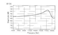
- FIG. 13A is a graph showing the relationship between vibration frequency and amplitude in the Z-axis sensor 7 of this embodiment.
- FIG. 13B is a graph showing the relationship between vibration frequency and amplitude in the Z-axis sensor 107 according to the reference example.
- the Z-axis sensor 7 of this embodiment can increase the resonance frequency of the movable portion compared to the Z-axis sensor 107 according to the reference example.
- FIG. 14 is a schematic plan view showing a modification of the Z-axis sensor.
- the same reference numerals as in FIG. 10 are given to the parts corresponding to those in FIG. 10 described above.
- the Z-axis sensor 7A of FIG. 14 differs from the Z-axis sensor 7 of FIG. 10 in the configurations of the fixed electrode structure and the movable electrode structure.
- the fixed electrode structure consists of a plurality of fixed electrodes 56 formed like comb teeth on the outer wall of the frame portion on the +X side of the fixed base portion 53 .
- the plurality of fixed electrodes 56 extend parallel to each other in the +X direction from the +X side frame portion of the fixed base portion 53 at equal intervals in the Y-axis direction.
- the movable electrode structure consists of a plurality of movable electrodes 60 formed like comb teeth on the inner wall of the +X-side frame of the movable base 57 .
- the plurality of movable electrodes 60 extend from the +X side frame portion of the movable base portion 57 toward between the fixed electrodes 56 adjacent to each other.
- the comb-teeth-shaped movable electrode 60 is arranged so as to mesh with the comb-teeth-shaped fixed electrode 56 without contacting the fixed electrode 56 .
Abstract
This acceleration sensor includes: a semiconductor substrate having a cavity formed in the interior thereof; a fixed structure including a fixed electrode supported by the semiconductor substrate in a state of floating in the cavity; and a movable structure including a movable electrode supported by the semiconductor substrate via an elastic structure in a state of floating in the cavity, the movable electrode being displaced relative to the fixed electrode. The elastic structure includes a first end section supported by the semiconductor substrate, a second end section connected to the movable structure, and an intermediate section connecting the first and second end sections. The elastic structure also has a linear portion extending linearly in at least part of the intermediate section. The linear portion is provided with a plurality of linear frames extending parallel to each other in the direction in which the linear portion extends.
Description
本開示は、加速度センサに関する。
The present disclosure relates to acceleration sensors.
物体に作用する加速度を計測するための加速度センサは、たとえば物体の姿勢や動き、振動状態などを把握するために広く用いられている。また、加速度センサには、小型化の要請が強い。このような要請に応えるべく、いわゆるMEMS(Micro Electro Mechanical System)の技術を用いて加速度センサの小型化が図られている。たとえば、特許文献1には、MEMS技術を用いた静電容量型の加速度センサが開示されている。
Acceleration sensors for measuring the acceleration acting on an object are widely used, for example, to grasp the posture, movement, vibration state, etc. of an object. In addition, there is a strong demand for miniaturization of acceleration sensors. In order to meet such demands, so-called MEMS (Micro Electro Mechanical System) technology is used to reduce the size of acceleration sensors. For example, Patent Literature 1 discloses a capacitive acceleration sensor using MEMS technology.
また、加速度センサには、高い加速度を検出できるように、検出可能な加速度の範囲を広くすること、また、加速度変化が高い周波数で生じても検出できるように、広帯域化することも要請されている。この2つの特性を向上させるには、加速度センサの可動部分の振動の共振周波数を高くする必要がある。
Acceleration sensors are also required to have a wide range of detectable acceleration so that they can detect high acceleration, and to have a wide band so that they can detect changes in acceleration even if they occur at high frequencies. there is In order to improve these two characteristics, it is necessary to increase the resonance frequency of the vibration of the movable portion of the acceleration sensor.
本開示の目的は、加速度センサの可動部分の振動の共振周波数を高くすることができる加速度センサを提供することである。
An object of the present disclosure is to provide an acceleration sensor capable of increasing the resonance frequency of vibration of the movable portion of the acceleration sensor.
本開示の一実施形態は、空洞が内部に形成された半導体基板と、前記空洞に対して浮いた状態で前記半導体基板に支持された固定電極を含む固定構造と、前記空洞に対して浮いた状態で前記半導体基板に弾性構造を介して支持され、前記固定電極に対して変位する可動電極を含む可動構造とを含み、前記弾性構造は、前記半導体基板に支持される第1端部と、前記可動構造に接続される第2端部と、前記第1端部と前記第2端部とを接続する中間部とを含み、前記中間部の少なくとも一部に直線状に延びた直線部分を有し、前記直線部分が、当該直線部分の延びる方向に互いに平行に延びた複数の直線フレームを備えている、加速度センサを提供する。
An embodiment of the present disclosure includes a semiconductor substrate having a cavity formed therein, a fixed structure including a fixed electrode supported by the semiconductor substrate in a state floating with respect to the cavity, and a fixed structure floating with respect to the cavity. a movable structure including a movable electrode supported by the semiconductor substrate via an elastic structure in a state and displaced relative to the fixed electrode, the elastic structure having a first end supported by the semiconductor substrate; a second end portion connected to the movable structure; and an intermediate portion connecting the first end portion and the second end portion; and the linear portion includes a plurality of linear frames extending parallel to each other in the direction in which the linear portion extends.
この構成では、加速度センサの可動部分の振動の共振周波数を高くすることができる。
With this configuration, it is possible to increase the resonance frequency of the vibration of the movable portion of the acceleration sensor.
本開示における上述の、またはさらに他の目的、特徴および効果は、添付図面を参照して次に述べる実施形態の説明により明らかにされる。
The above and further objects, features and effects of the present disclosure will be made clear by the following description of the embodiments with reference to the accompanying drawings.
[本開示の実施形態の説明]
本開示の一実施形態は、空洞が内部に形成された半導体基板と、前記空洞に対して浮いた状態で前記半導体基板に支持された固定電極を含む固定構造と、前記空洞に対して浮いた状態で前記半導体基板に弾性構造を介して支持され、前記固定電極に対して変位する可動電極を含む可動構造とを含み、前記弾性構造は、前記半導体基板に支持される第1端部と、前記可動構造に接続される第2端部と、前記第1端部と前記第2端部とを接続する中間部とを含み、前記中間部の少なくとも一部に直線状に延びた直線部分を有し、前記直線部分が、当該直線部分の延びる方向に互いに平行に延びた複数の直線フレームを備えている、加速度センサを提供する。 [Description of Embodiments of the Present Disclosure]
An embodiment of the present disclosure includes a semiconductor substrate having a cavity formed therein, a fixed structure including a fixed electrode supported by the semiconductor substrate in a state floating with respect to the cavity, and a fixed structure floating with respect to the cavity. a movable structure including a movable electrode supported by the semiconductor substrate via an elastic structure in a state and displaced relative to the fixed electrode, the elastic structure having a first end supported by the semiconductor substrate; a second end portion connected to the movable structure; and an intermediate portion connecting the first end portion and the second end portion; and the linear portion includes a plurality of linear frames extending parallel to each other in the direction in which the linear portion extends.
この構成では、加速度センサの可動部分の振動の共振周波数を高くすることができる。
With this configuration, it is possible to increase the resonance frequency of the vibration of the movable portion of the acceleration sensor.
本開示の一実施形態では、前記直線部分は、当該直線部分に含まれる前記複数の直線フレーム間に架設された複数の補強フレームを含む。
In one embodiment of the present disclosure, the straight portion includes a plurality of reinforcing frames installed between the plurality of straight frames included in the straight portion.
本開示の一実施形態では、前記直線部分は、当該直線部分に含まれる前記複数の直線フレーム間に、当該直線フレームに沿って三角形状の空間が繰り返されるように、前記複数の直線フレーム間に架設された複数の補強フレームを含む。
In one embodiment of the present disclosure, the linear portion includes a linear frame between the linear frames such that a triangular space is repeated along the linear frame. Includes multiple stiffening frames suspended.
本開示の一実施形態では、前記直線部分は、互いに平行に延びた第1直線部分および第2直線部分と、前記第1直線部分および前記第2直線部分の一端どうしを連結する第3直線部分とを含む。
In one embodiment of the present disclosure, the linear portion includes a first linear portion and a second linear portion extending parallel to each other, and a third linear portion connecting one ends of the first linear portion and the second linear portion. including.
本開示の一実施形態では、前記第1直線部分、前記第2直線部分および前記第3直線部分は、それぞれ、それらに含まれている前記複数の直線フレーム間に架設された少なくとも1つの補強フレームを含む。
In one embodiment of the present disclosure, each of said first straight portion, said second straight portion and said third straight portion includes at least one reinforcing frame spanning between said plurality of straight frames included therein. including.
本開示の一実施形態では、前記直線部分が、前記可動電極の延びる方向に対して平行な直線部分を含む。
In one embodiment of the present disclosure, the linear portion includes a linear portion parallel to the extending direction of the movable electrode.
本開示の一実施形態では、前記固定電極が、所定の第1方向に間隔をおいて、前記第1方向と直交する第2方向に互いに平行に延びた一対の固定電極を含み、前記可動電極が、前記一対の固定電極の間に配置され、前記第1方向に間隔をおいて、前記第2方向に互いに平行に延びた1対の可動電極を含む。
In one embodiment of the present disclosure, the fixed electrode includes a pair of fixed electrodes extending parallel to each other in a second direction orthogonal to the first direction with an interval in a predetermined first direction, and the movable electrode includes a pair of movable electrodes disposed between said pair of fixed electrodes, spaced apart in said first direction and extending parallel to each other in said second direction.
本開示の一実施形態では、前記固定電極が、平面視において、櫛歯状に形成された複数の固定電極を含み、前記可動電極が、平面視において、櫛歯状に形成された複数の可動電極対を含み、前記複数の可動電極対は、前記複数の固定電極に対して、接触しないで噛み合うように配置されており、前記各可動電極対は、当該可動電極対の両側の前記固定電極にそれぞれ対向し、かつ互いに平行に延びた2つの前記可動電極を含む。
In one embodiment of the present disclosure, the fixed electrode includes a plurality of fixed electrodes formed in a comb shape in plan view, and the movable electrode includes a plurality of movable electrodes formed in a comb shape in plan view. an electrode pair, wherein the plurality of movable electrode pairs are disposed in non-contacting engagement with the plurality of fixed electrodes, each movable electrode pair being aligned with the fixed electrodes on opposite sides of the movable electrode pair; and extending parallel to each other.
本開示の一実施形態では、前記固定電極の横断面形状および前記可動電極の横断面形状が、上下方向に細長い四角形状である。
In one embodiment of the present disclosure, the cross-sectional shape of the fixed electrode and the cross-sectional shape of the movable electrode are squares elongated in the vertical direction.
本開示の一実施形態では、前記弾性構造は、1つ前記直線部分と、前記直線部分の一端に接続されたテーパ部分とを含み、当該直線部分は、互いに平行な2つの前記直線フレームからなり、前記テーパ部分は、該2つの前記直線フレームの一端部のそれぞれから、互いの間隔が徐々に広がるように、当該2つの前記直線フレームに対して斜め外方に延びた2本の接続フレームからなる。
In one embodiment of the present disclosure, the elastic structure includes one straight portion and a tapered portion connected to one end of the straight portion, the straight portion consisting of two parallel straight frames. , the tapered portion is formed from two connection frames extending obliquely outward with respect to the two linear frames such that the distance between the two connecting frames gradually widens from one end of each of the two linear frames. Become.
本開示の一実施形態では、前記直線部分が、前記可動電極の延びる方向に対して平行であるか、または、前記半導体基板の表面に沿う方向であって、前記可動電極の延びる方向と直交する方向に対して平行である。
In one embodiment of the present disclosure, the linear portion is parallel to the extending direction of the movable electrode, or is a direction along the surface of the semiconductor substrate and orthogonal to the extending direction of the movable electrode. parallel to the direction.
本開示の一実施形態では、前記固定電極が、平面視において、櫛歯状に形成された複数の固定電極を含み、前記可動電極が、平面視において、櫛歯状に形成された複数の可動電極を含み、前記複数の可動電極は、前記複数の固定電極に対して、接触しないで噛み合うように配置されている。
In one embodiment of the present disclosure, the fixed electrode includes a plurality of fixed electrodes formed in a comb shape in plan view, and the movable electrode includes a plurality of movable electrodes formed in a comb shape in plan view. The plurality of movable electrodes are arranged in non-contacting engagement with the plurality of fixed electrodes.
本開示の一実施形態では、前記固定電極の横断面形状および前記可動電極の横断面形状が、上下方向に細長い四角形状である。
In one embodiment of the present disclosure, the cross-sectional shape of the fixed electrode and the cross-sectional shape of the movable electrode are squares elongated in the vertical direction.
本開示の一実施形態では、前記固定電極および前記可動電極のうちのいずれか一方は、他方に対して下方にずれた状態に配置されている。
In one embodiment of the present disclosure, one of the fixed electrode and the movable electrode is arranged in a downwardly displaced state with respect to the other.
[本開示の実施形態の詳細な説明]
以下では、本開示の実施の形態を、添付図面を参照して詳細に説明する。 [Detailed Description of Embodiments of the Present Disclosure]
Embodiments of the present disclosure are described in detail below with reference to the accompanying drawings.
以下では、本開示の実施の形態を、添付図面を参照して詳細に説明する。 [Detailed Description of Embodiments of the Present Disclosure]
Embodiments of the present disclosure are described in detail below with reference to the accompanying drawings.
[1]加速度センサの全体構成
図1は、本開示の一実施形態に係る加速度センサを示す図解的な平面図である。 [1] Overall Configuration of Acceleration Sensor FIG. 1 is an illustrative plan view showing an acceleration sensor according to an embodiment of the present disclosure.
図1は、本開示の一実施形態に係る加速度センサを示す図解的な平面図である。 [1] Overall Configuration of Acceleration Sensor FIG. 1 is an illustrative plan view showing an acceleration sensor according to an embodiment of the present disclosure.
説明の便宜上、以下では、図1~図4に示した+X方向、-X方向、+Y方向、-Y方向、+Z方向および-Z方向を用いることがある。+X方向は、平面視において、半導体基板2の表面に沿う所定の方向であり、+Y方向は、平面視において半導体基板2の表面に沿う方向あって、+X方向に直交する方向である。+Z方向は、半導体基板2の厚さに沿う方向あって、+X方向および+Y方向に直交する方向である。
For convenience of explanation, hereinafter, the +X direction, -X direction, +Y direction, -Y direction, +Z direction and -Z direction shown in FIGS. 1 to 4 may be used. The +X direction is a predetermined direction along the surface of the semiconductor substrate 2 in plan view, and the +Y direction is a direction along the surface of the semiconductor substrate 2 in plan view and orthogonal to the +X direction. The +Z direction is a direction along the thickness of the semiconductor substrate 2 and perpendicular to the +X direction and the +Y direction.
-X方向は、+X方向と反対の方向である。-Y方向は、+Y方向と反対の方向である。-Z方向は、+Z方向と反対の方向である。+X方向および-X方向を総称するときには「X軸方向」という。+Y方向および-Y方向を総称するときには「Y軸方向」という。+Z方向および-Z方向を総称するときには「Z軸方向」という。
The -X direction is the direction opposite to the +X direction. The -Y direction is the opposite direction to the +Y direction. The -Z direction is the direction opposite to the +Z direction. The +X direction and the -X direction are collectively referred to as the "X-axis direction". The +Y direction and the -Y direction are collectively referred to as the "Y-axis direction". The +Z direction and the −Z direction are collectively referred to as the “Z-axis direction”.
加速度センサ1は、平面視四角形状の半導体基板2と、半導体基板2の中央部に配置されたセンサ部3と、半導体基板2におけるセンサ部3の側方に配置された電極パッド4とを含んでいる。加速度センサ1は、静電容量型加速度センサである。半導体基板2は、平面視でX軸方向に平行な2辺とY軸方向に平行な2辺とを有する四角形状を有している。
The acceleration sensor 1 includes a semiconductor substrate 2 having a square shape in plan view, a sensor section 3 arranged in the center of the semiconductor substrate 2, and electrode pads 4 arranged on the sides of the sensor section 3 on the semiconductor substrate 2. I'm in. The acceleration sensor 1 is a capacitive acceleration sensor. The semiconductor substrate 2 has a rectangular shape having two sides parallel to the X-axis direction and two sides parallel to the Y-axis direction in plan view.
センサ部3は、三次元空間において直交する3つの軸に沿う方向に作用する加速度をそれぞれ検出するセンサとして、X軸センサ5、Y軸センサ6およびZ軸センサ7を有している。X軸センサ5は、X軸方向に作用する加速度を検出するためのものである。Y軸センサ6は、Y軸方向の加速度を検出するためのものである。Z軸センサ7は、Z軸方向の加速度を検出するためのものである。
The sensor unit 3 has an X-axis sensor 5, a Y-axis sensor 6, and a Z-axis sensor 7 as sensors for detecting acceleration acting along three orthogonal axes in a three-dimensional space. The X-axis sensor 5 is for detecting acceleration acting in the X-axis direction. The Y-axis sensor 6 is for detecting acceleration in the Y-axis direction. The Z-axis sensor 7 is for detecting acceleration in the Z-axis direction.
半導体基板2は、導電性シリコン基板(たとえば、5Ω・m~500Ω・mの抵抗率を有する低抵抗基板)からなる。この半導体基板2は、内部に空洞10(図4参照)を有しており、空洞10を表面側から区画する天面を有する半導体基板2の上壁(表層部)11にX軸センサ5、Y軸センサ6およびZ軸センサ7が形成されている。
The semiconductor substrate 2 is made of a conductive silicon substrate (for example, a low resistance substrate having a resistivity of 5Ω·m to 500Ω·m). The semiconductor substrate 2 has a cavity 10 (see FIG. 4) inside, and an X-axis sensor 5, an X-axis sensor 5, and an X-axis sensor 5 are mounted on an upper wall (surface layer) 11 of the semiconductor substrate 2 having a top surface that partitions the cavity 10 from the surface side. A Y-axis sensor 6 and a Z-axis sensor 7 are formed.
つまり、X軸センサ5、Y軸センサ6およびZ軸センサ7は半導体基板2の一部からなり、空洞10を裏面側から区画する底面を有する半導体基板2の底壁12(図4参照)に対して浮いた状態で支持されている。
That is, the X-axis sensor 5, the Y-axis sensor 6, and the Z-axis sensor 7 are part of the semiconductor substrate 2, and are attached to the bottom wall 12 (see FIG. 4) of the semiconductor substrate 2 having a bottom surface that defines the cavity 10 from the back side. It is supported in a floating state.
X軸センサ5およびY軸センサ6は、X軸方向に間隔を空けて互いに隣接して配置されている。X軸センサ5およびY軸センサ6のそれぞれを取り囲むように、2つのZ軸センサ7が配置されている。この実施形態では、Y軸センサ6は、X軸センサ5を平面視で90°回転させたものとほぼ同様の構成を有している。
The X-axis sensor 5 and the Y-axis sensor 6 are arranged adjacent to each other with an interval in the X-axis direction. Two Z-axis sensors 7 are arranged to surround each of the X-axis sensor 5 and the Y-axis sensor 6 . In this embodiment, the Y-axis sensor 6 has substantially the same configuration as the X-axis sensor 5 rotated by 90° in plan view.
これら3つのセンサ5~7は、たとえばシリコン基板からなる蓋8が半導体基板2の表面に接合されることにより、蓋8により覆われて密閉されている。
These three sensors 5 to 7 are covered and hermetically sealed by a lid 8 made of, for example, a silicon substrate and bonded to the surface of the semiconductor substrate 2 .
電極パッド4は、外部の電子部品に接続されて、各センサ5~7に信号を入力したり、各センサ5~7から信号を出力したりするものであり、必要数(図1では、9つ)設けられている。外部の電子部品は、たとえば、ASIC(Application Specific Integrated Circuit)素子である。
The electrode pads 4 are connected to external electronic components to input signals to the sensors 5-7 and output signals from the sensors 5-7. 1) is provided. The external electronic component is, for example, an ASIC (Application Specific Integrated Circuit) element.
[2]X軸センサ5
図2は、主としてX軸センサを示す図解的な平面図である。図3は、図2の要部拡大平面図である。図4は、図3のIV-IV線に沿う図解的な拡大断面図である。図5Aは、図3のバネ部を示す図解的な拡大平面図である。 [2]X-axis sensor 5
FIG. 2 is a schematic plan view mainly showing the X-axis sensor. 3 is an enlarged plan view of a main part of FIG. 2. FIG. 4 is a schematic enlarged cross-sectional view taken along line IV-IV of FIG. 3. FIG. 5A is a schematic enlarged plan view showing the spring portion of FIG. 3; FIG.
図2は、主としてX軸センサを示す図解的な平面図である。図3は、図2の要部拡大平面図である。図4は、図3のIV-IV線に沿う図解的な拡大断面図である。図5Aは、図3のバネ部を示す図解的な拡大平面図である。 [2]
FIG. 2 is a schematic plan view mainly showing the X-axis sensor. 3 is an enlarged plan view of a main part of FIG. 2. FIG. 4 is a schematic enlarged cross-sectional view taken along line IV-IV of FIG. 3. FIG. 5A is a schematic enlarged plan view showing the spring portion of FIG. 3; FIG.
X軸センサ5とZ軸センサ7との間には、X軸センサ5を浮いた状態に支持するための支持部14が形成されている。支持部14は、半導体基板2の空洞10を横側から区画する側面を有する一側壁15の上部から、Z軸センサ7を横切ってX軸センサ5へ向かって延びる支持ベース部16と、X軸センサ5を取り囲む環状部17とを一体的に含んでいる。支持部14は、半導体基板2の底壁12から浮いた状態で、半導体基板2の一側壁15に支持されている。
A support portion 14 is formed between the X-axis sensor 5 and the Z-axis sensor 7 to support the X-axis sensor 5 in a floating state. The support portion 14 includes a support base portion 16 extending across the Z-axis sensor 7 toward the X-axis sensor 5 from the upper portion of one side wall 15 having a side surface that laterally partitions the cavity 10 of the semiconductor substrate 2; An annular portion 17 surrounding the sensor 5 is integrally included. The supporting portion 14 is supported by one side wall 15 of the semiconductor substrate 2 while floating from the bottom wall 12 of the semiconductor substrate 2 .
支持ベース部16は、平面視でY軸方向に長い四角形状である。環状部17は、平面視で矩形環状であり、-Y側の第1枠部17A、-X側の第2枠部17B、+Y側の第3枠部17Cおよび+X側の第4枠部17Dを含む。ただし、第1枠部17Aは、長さ中央部で分断されている。第2枠部17Bの長さ中央部が、支持ベース部16に連結されている。X軸センサ5は、環状部17の内側に配置され、環状部17に支持されている。
The support base portion 16 has a rectangular shape elongated in the Y-axis direction in a plan view. The annular portion 17 has a rectangular annular shape in plan view, and includes a first frame portion 17A on the −Y side, a second frame portion 17B on the −X side, a third frame portion 17C on the +Y side, and a fourth frame portion 17D on the +X side. including. However, the first frame portion 17A is divided at the length center portion. A length center portion of the second frame portion 17B is connected to the support base portion 16 . The X-axis sensor 5 is arranged inside the annular portion 17 and supported by the annular portion 17 .
X軸センサ5は、空洞10内に設けられた支持部14に固定された固定構造21と、固定構造21に対して振動可能に保持された可動構造22とを有している。固定構造21および可動構造22は、同じ厚さで形成されている。
The X-axis sensor 5 has a fixed structure 21 fixed to the support portion 14 provided in the cavity 10 and a movable structure 22 held vibratably with respect to the fixed structure 21 . The fixed structure 21 and the movable structure 22 are formed with the same thickness.
固定構造21は、固定ベース部23と、複数の固定電極24とを含む。
The fixed structure 21 includes a fixed base portion 23 and a plurality of fixed electrodes 24 .
固定ベース部23は、第1枠部17Aの内側壁に沿ってX軸方向に延びており、支持部14に固定されている。固定ベース部23は、互いに平行に延びる複数(この実施形態では2本)のメインフレームと、複数のメインフレーム間に架設された複数のサブフレームとを含む、平面視梯子状の骨組み構造を有している。
The fixed base portion 23 extends in the X-axis direction along the inner wall of the first frame portion 17A and is fixed to the support portion 14 . The fixed base portion 23 has a ladder-like frame structure in a plan view, including a plurality of (two in this embodiment) main frames extending parallel to each other and a plurality of sub-frames installed between the plurality of main frames. doing.
複数の固定電極24は、固定ベース部23の内側壁に櫛歯状に形成されている。複数の固定電極24は、X軸方向に等間隔を空けて、互いに平行に配置されている。つまり、複数の固定電極24は、固定ベース部23から+Y方向に延びている。
A plurality of fixed electrodes 24 are formed in a comb shape on the inner wall of the fixed base portion 23 . The plurality of fixed electrodes 24 are arranged parallel to each other at regular intervals in the X-axis direction. That is, the fixed electrodes 24 extend in the +Y direction from the fixed base portion 23 .
可動構造22は、可動ベース部26と、複数の可動電極部27とを含む。
The movable structure 22 includes a movable base portion 26 and a plurality of movable electrode portions 27 .
可動ベース部26は、第3枠部17Cの内側壁に沿ってX軸方向に延びている。可動ベース部26の両端が、X軸方向に沿って伸縮自在なバネ部25を介して固定ベース部23に接続されている。バネ部25は、本発明の「弾性構造」の一例である。
The movable base portion 26 extends in the X-axis direction along the inner wall of the third frame portion 17C. Both ends of the movable base portion 26 are connected to the fixed base portion 23 via spring portions 25 that are extendable along the X-axis direction. The spring portion 25 is an example of the "elastic structure" of the present invention.
可動ベース部26は、X軸方向に平行に延びる複数(この実施形態では5本)のメインフレーム26Aと、複数のメインフレーム26A間に架設された複数のサブフレーム26Bとを含む、平面視格子状の骨組み構造を有している。
The movable base portion 26 includes a plurality of (five in this embodiment) main frames 26A extending parallel to the X-axis direction, and a plurality of sub-frames 26B installed between the plurality of main frames 26A. It has a shaped frame structure.
複数の可動電極部27は可動ベース部26の内側壁に櫛歯状に形成されている。複数の可動電極部27は、X軸方向に等間隔を空けて互いに平行に配置されている。複数の可動電極部27は、可動ベース部26から、互いに隣接する固定電極24間に向かって延びている。つまり、櫛歯状の可動電極部27は、櫛歯状の固定電極24に対して、固定電極24と接触しないで噛み合うように配置されている。
A plurality of movable electrode portions 27 are formed in a comb shape on the inner wall of the movable base portion 26 . The plurality of movable electrode portions 27 are arranged parallel to each other at equal intervals in the X-axis direction. A plurality of movable electrode portions 27 extend from the movable base portion 26 toward between the fixed electrodes 24 adjacent to each other. That is, the comb tooth-shaped movable electrode portion 27 is arranged so as to mesh with the comb tooth-shaped fixed electrode 24 without coming into contact with the fixed electrode 24 .
各可動電極部27は、可動ベース部26内の隣合う一対のサブフレーム26Bの-Y側端それぞれから-Y方向に互いに平行に延びた第1可動電極27Aおよび第2可動電極27Bと、それらを連結する複数の連結部27Cとを含む。各連結部27Cの長さ中間部は、酸化シリコン(SiO2)からなる第1隔離結合部(絶縁層)91によって構成されている。これにより、第1可動電極27Aと第2可動電極27Bとは電気的に絶縁されている。
Each movable electrode portion 27 includes a first movable electrode 27A and a second movable electrode 27B extending parallel to each other in the −Y direction from the −Y side ends of a pair of adjacent sub-frames 26B in the movable base portion 26, and and a plurality of connecting portions 27C that connect the . A length intermediate portion of each connecting portion 27C is constituted by a first isolated coupling portion (insulating layer) 91 made of silicon oxide (SiO 2 ). Thereby, the first movable electrode 27A and the second movable electrode 27B are electrically insulated.
可動電極部27に含まれている第1可動電極27Aおよび第2可動電極27Bは、本発明の「可動電極対」の一例である。
The first movable electrode 27A and the second movable electrode 27B included in the movable electrode portion 27 are examples of the "movable electrode pair" of the present invention.
固定電極24および可動電極27A,27Bの横断面形状は、図4に示されるように、Z軸方向に細長い四角形状である。言い換えれば、固定電極24および可動電極27A,27Bは、厚さ方向がX軸方向である板状である。
The cross-sectional shape of the fixed electrode 24 and the movable electrodes 27A and 27B is, as shown in FIG. 4, a rectangular shape elongated in the Z-axis direction. In other words, the fixed electrode 24 and the movable electrodes 27A and 27B are plate-shaped with the thickness direction being the X-axis direction.
以下において、第1可動電極27Aが接続されたサブフレームを、「第1可動サブフレーム26Ba」といい、第2可動電極27Bが接続されたサブフレームを、「第2可動サブフレーム26Bb」という場合がある。
Hereinafter, the subframe to which the first movable electrode 27A is connected will be referred to as the "first movable subframe 26Ba", and the subframe to which the second movable electrode 27B is connected will be referred to as the "second movable subframe 26Bb". There is
メインフレーム26Aにおける、隣接する2つのサブフレーム26Bを連結している部分の長さ中間部は、酸化シリコンからなる第2隔離結合部(絶縁層)92によって構成されている。したがって、各サブフレーム26Bは、他のサブフレーム26Bから電気的に絶縁されている。第1隔離結合部91および第2隔離結合部92によって、各可動電極27A,27Bは、他の可動電極27A,27Bから電気的に絶縁されている。
A second isolating joint (insulating layer) 92 made of silicon oxide is formed in the main frame 26A at the intermediate length of the portion connecting two adjacent sub-frames 26B. Therefore, each subframe 26B is electrically isolated from other subframes 26B. Each movable electrode 27A, 27B is electrically insulated from the other movable electrodes 27A, 27B by the first isolation joint 91 and the second isolation joint 92 .
第1可動電極27Aは、第2可動電極27Bに対して-X側に配置されている。X軸方向の加速度が作用していない状態では、第1可動電極27Aとこれに隣接する固定電極24との間隔は、第2可動電極27Bとこれに隣接する固定電極24との間隔に等しい。
The first movable electrode 27A is arranged on the -X side with respect to the second movable electrode 27B. When no acceleration in the X-axis direction is applied, the distance between the first movable electrode 27A and the fixed electrode 24 adjacent thereto is equal to the distance between the second movable electrode 27B and the fixed electrode 24 adjacent thereto.
-X側に配置されたバネ部25および+Y側に配置されたバネ部25のーY側端部は、長さ中間部が酸化シリコンからなる第3隔離結合部(絶縁層)93によって構成されている連結フレームを介して、固定ベース部23に機械的に接続されている。したがって、固定ベース部23とバネ部25とは、電気的に絶縁されている。
The -Y side ends of the spring portion 25 arranged on the -X side and the spring portion 25 arranged on the +Y side are constituted by a third isolation coupling portion (insulating layer) 93 made of silicon oxide in the middle of the length. It is mechanically connected to the fixed base portion 23 via the connecting frame. Therefore, the fixed base portion 23 and the spring portion 25 are electrically insulated.
-X側に配置されたバネ部25の+Y側端は、最も-X側にある第1可動サブフレーム26Baに機械的および電気的に接続されている。+X側に配置されたバネ部25の+Y側端は、最も+X側にある第2可動サブフレーム26Bbに機械的および電気的に接続されている。これらのバネ部25は、可動ベース部26をX軸方向に移動可能に支持するバネとして機能するとともに、導電経路としても機能する。
The +Y side end of the spring portion 25 arranged on the -X side is mechanically and electrically connected to the first movable sub-frame 26Ba on the most -X side. The +Y side end of the spring portion 25 arranged on the +X side is mechanically and electrically connected to the second movable sub-frame 26Bb on the most +X side. These spring portions 25 function as springs that support the movable base portion 26 so as to be movable in the X-axis direction, and also function as conductive paths.
固定構造21および可動構造22を含む半導体基板2の表面には、図示しない絶縁膜が形成されている。当該絶縁膜の表面には、図示しない複数の配線が形成されている。複数の配線は、複数の固定電極24を固定電極用の電極パッド4に電気的に接続するための第1配線、複数の第1可動電極27Aを第1可動電極用の電極パッド4に電気的に接続するための第2配線、複数の第2可動電極27Bを第2可動電極用の電極パッド4に電気的に接続するための第3配線を含む。
An insulating film (not shown) is formed on the surface of the semiconductor substrate 2 including the fixed structure 21 and the movable structure 22 . A plurality of wirings (not shown) are formed on the surface of the insulating film. The plurality of wirings are the first wiring for electrically connecting the plurality of fixed electrodes 24 to the electrode pad 4 for the fixed electrode, and the plurality of first movable electrodes 27A for electrically connecting the electrode pad 4 for the first movable electrode. and a third wiring for electrically connecting the plurality of second movable electrodes 27B to the electrode pads 4 for the second movable electrodes.
第2配線は、複数の第1可動サブフレーム26Baを互いに電気的に接続するための配線および-X側のバネ部25を第1可動電極用の電極パッド4に電気的に接続するための配線を含む。第3配線は、複数の第2可動サブフレーム26Bbを互いに電気的に接続するための配線および+X側のバネ部25を第2可動電極用の電極パッド4に電気的に接続するための配線を含む。
The second wiring is wiring for electrically connecting the plurality of first movable sub-frames 26Ba to each other and wiring for electrically connecting the -X side spring portion 25 to the electrode pad 4 for the first movable electrode. including. The third wiring includes wiring for electrically connecting the plurality of second movable sub-frames 26Bb to each other and wiring for electrically connecting the spring portion 25 on the +X side to the electrode pad 4 for the second movable electrode. include.
本実施形態においては、X軸センサ5のX軸方向およびY軸方向の長さは、例えば300μm程度である。X軸センサ5の+Z側表面から半導体基板2の底壁12(図4参照)の内面(+Z側表面)までのZ軸方向長さは、例えば50μm程度である。X軸センサ5の+Z側表面から半導体基板2の底壁12の外面(-Z側表面)までのZ軸方向長さは、例えば200μm~300μm程度である。また、固定電極24、第1可動電極27Aおよび第2可動電極27BのZ軸方向の長さは、例えば15μm~30μm程度である。
In this embodiment, the lengths of the X-axis sensor 5 in the X-axis direction and the Y-axis direction are, for example, about 300 μm. The length in the Z-axis direction from the +Z-side surface of the X-axis sensor 5 to the inner surface (+Z-side surface) of the bottom wall 12 (see FIG. 4) of the semiconductor substrate 2 is, for example, about 50 μm. The length in the Z-axis direction from the +Z-side surface of the X-axis sensor 5 to the outer surface (-Z-side surface) of the bottom wall 12 of the semiconductor substrate 2 is, for example, about 200 μm to 300 μm. Also, the lengths of the fixed electrode 24, the first movable electrode 27A and the second movable electrode 27B in the Z-axis direction are, for example, about 15 μm to 30 μm.
X軸センサ5では、X軸方向の加速度が作用した場合、2つのバネ部25に支持された可動ベース部26がX軸方向に振動する。これにより、可動ベース部26から延びる第1可動電極27Aおよび第2可動電極27Bも、互いに隣接する2つの固定電極24の間で、X軸方向に振動する。可動ベース部26が+X方向に移動した場合、第1可動電極27Aは隣接する固定電極24から離れた位置に移動し、第2可動電極27Bは隣接する固定電極24に近づく位置に移動する。逆に、可動ベース部26が-X方向に移動した場合、第1可動電極27Aは隣接する固定電極24に近づく位置に移動し、第2可動電極27Bは隣接する固定電極24から離れた位置に移動する。
In the X-axis sensor 5, when acceleration in the X-axis direction acts, the movable base portion 26 supported by the two spring portions 25 vibrates in the X-axis direction. As a result, the first movable electrode 27A and the second movable electrode 27B extending from the movable base portion 26 also vibrate in the X-axis direction between the two fixed electrodes 24 adjacent to each other. When the movable base portion 26 moves in the +X direction, the first movable electrode 27A moves away from the adjacent fixed electrode 24, and the second movable electrode 27B moves closer to the adjacent fixed electrode 24. Conversely, when the movable base portion 26 moves in the -X direction, the first movable electrode 27A moves closer to the adjacent fixed electrode 24, and the second movable electrode 27B moves away from the adjacent fixed electrode 24. Moving.
これにより、第1可動電極27Aとそれに隣接する固定電極24との対向距離d1および第2可動電極27Bとそれに隣接する固定電極24との対向距離d2とが変化する。そして、対向距離d1の変化に起因する第1可動電極27A/固定電極24間の静電容量C1の変化および対向距離d2の変化に起因する第2可動電極27B/固定電極24間の静電容量C2の変化を検出することによって、X軸方向の加速度が検出される。
As a result, the facing distance d1 between the first movable electrode 27A and the fixed electrode 24 adjacent thereto and the facing distance d2 between the second movable electrode 27B and the fixed electrode 24 adjacent thereto change. A change in capacitance C1 between the first movable electrode 27A/fixed electrode 24 due to a change in the facing distance d1 and a change in capacitance C1 between the second movable electrode 27B/fixed electrode 24 due to a change in the facing distance d2 Acceleration in the X-axis direction is detected by detecting a change in C2.
図3および図5Aを参照して、-X側のバネ部25は、Y軸方向に延びた直線部分30から構成されている。直線部分30は、Y軸方向に平行に延びた2本の直線フレーム31と、当該直線フレーム31間に架設された複数の補強フレーム32を含む。補強フレーム32は、2本の直線フレーム31の-Y方向端どうしを連結する第1補強フレーム32Aと、2本の直線フレーム31の+Y方向端どうしを連結する第2補強フレーム32Bと、2本の直線フレーム31の長さ方向中間部どうしを連結する複数の第3補強フレーム32Cとを含む。
3 and 5A, the -X side spring portion 25 is composed of a straight portion 30 extending in the Y-axis direction. The straight portion 30 includes two straight frames 31 extending in parallel in the Y-axis direction and a plurality of reinforcing frames 32 installed between the straight frames 31 . There are two reinforcing frames 32: a first reinforcing frame 32A connecting the ends of the two linear frames 31 in the -Y direction, and a second reinforcing frame 32B connecting the ends of the two linear frames 31 in the +Y direction. and a plurality of third reinforcing frames 32C that connect the lengthwise intermediate portions of the straight frames 31 to each other.
第1補強フレーム32Aの+X側端には、+X方向に延びた第1接続部33が連結されている。第2補強フレーム32Bの+X側端には、+X方向に延びた第2接続部34が連結されている。バネ部25(直線部分30)の-Y側端は、第1接続部33を介して固定ベース部23に機械的に接続されている。バネ部25(直線部分30)の+Y側端は、第2接続部34を介して第1可動サブフレーム26Baに機械的および電気的に接続されている。
A first connecting portion 33 extending in the +X direction is connected to the +X side end of the first reinforcing frame 32A. A second connecting portion 34 extending in the +X direction is connected to the +X side end of the second reinforcing frame 32B. The −Y side end of the spring portion 25 (linear portion 30 ) is mechanically connected to the fixed base portion 23 via the first connection portion 33 . The +Y side end of the spring portion 25 (linear portion 30) is mechanically and electrically connected to the first movable sub-frame 26Ba via the second connection portion .
+X側に配置されたバネ部25は、-X側のバネ部25と+X側のバネ部25との間の中央を通りかつY軸方向に延びる直線に対して、-X側のバネ部25と線対称の平面形状を有している。したがって、+X側のバネ部25においては、第1補強フレーム32Aの-X側端に、-X方向に延びた第1接続部33が連結され、第2補強フレーム32Bの-X側端に、-X方向に延びた第2接続部34が連結されている。+X側のバネ部25(直線部分30)の-Y側端は、第1接続部33を介して固定ベース部23に機械的に接続されている。+X側のバネ部25(直線部分30)の+Y側端は、第2接続部34を介して第2可動サブフレーム26Bbに機械的および電気的に接続されている。
The spring portion 25 arranged on the +X side is located at the -X side spring portion 25 with respect to a straight line passing through the center between the -X side spring portion 25 and the +X side spring portion 25 and extending in the Y-axis direction. It has a planar shape that is symmetrical with Therefore, in the +X side spring portion 25, the first connecting portion 33 extending in the -X direction is connected to the -X side end of the first reinforcing frame 32A, and the -X side end of the second reinforcing frame 32B is connected to A second connecting portion 34 extending in the -X direction is connected. The −Y side end of the +X side spring portion 25 (linear portion 30 ) is mechanically connected to the fixed base portion 23 via the first connection portion 33 . The +Y side end of the +X side spring portion 25 (linear portion 30) is mechanically and electrically connected to the second movable sub-frame 26Bb via the second connection portion .
図6は、X軸センサの参考例を示す図解的な要部拡大平面図である。図6において、前述の図3の各部に対応する部分には、図3と同じ符号を付して示す。図5Dは、図6に示される参考例に係るX軸センサに用いられているバネ部を示す図解的な拡大平面図である。
FIG. 6 is an illustrative main part enlarged plan view showing a reference example of the X-axis sensor. In FIG. 6, the same reference numerals as in FIG. 3 denote the parts corresponding to the parts in FIG. 3 described above. 5D is an illustrative enlarged plan view showing a spring portion used in the X-axis sensor according to the reference example shown in FIG. 6. FIG.
参考例に係るX軸センサ105に用いられている-X側のバネ部125は、Y軸方向に延びた1本の直線フレームからなる直線部分131から構成されている。直線部分131の-Y方向端には、直線部分131の-Y方向端から+X方向に延びる第1接続部132が連結されている。直線部分131の+Y方向端には、直線部分131の+Y方向端から+X方向に延びた後、-Y方向に延びる平面視鈎形の第2接続部133が連結されている。バネ部125(直線部分131)の-Y側端は、第1接続部132介して固定ベース部23に機械的に接続される。バネ部125(直線部分131)の+Y側端は、第2接続部133を介して第2可動サブフレーム26Bbに機械的および電気的に接続される。
The -X side spring portion 125 used in the X-axis sensor 105 according to the reference example is composed of a linear portion 131 made up of a single linear frame extending in the Y-axis direction. A first connecting portion 132 extending in the +X direction from the -Y direction end of the straight portion 131 is connected to the -Y direction end of the straight portion 131 . The +Y direction end of the straight portion 131 is connected to a hook-shaped second connection portion 133 extending in the -Y direction after extending in the +X direction from the +Y direction end of the straight portion 131 . The −Y side end of the spring portion 125 (linear portion 131 ) is mechanically connected to the fixed base portion 23 via the first connection portion 132 . The +Y side end of the spring portion 125 (linear portion 131) is mechanically and electrically connected to the second movable sub-frame 26Bb via the second connection portion 133. As shown in FIG.
+X側に配置されるバネ部125は、-X側のバネ部125と-X側のバネ部125との間の中央を通りかつY軸方向に延びる直線に対して、-X側のバネ部125と線対称の平面形状を有している。+X側のバネ部125においては、1本の直線フレームからなる直線部分131の-Y側端に、-X方向に延びた第1接続部132が連結され、直線部分131の+Y側端に、-X方向に延びた後、-Y方向に延びた平面視鈎形の第2接続部133が連結されている。+X側のバネ部125(直線部分131)の-Y側端は、第1接続部132を介して固定ベース部23に機械的に接続される。+X側のバネ部125(直線部分131)の+Y側端は、第2接続部133を介して第1可動サブフレーム26Baに機械的および電気的に接続される。
The spring portion 125 arranged on the +X side is located on the -X side with respect to a straight line passing through the center between the -X side spring portion 125 and the -X side spring portion 125 and extending in the Y-axis direction. 125 and has a plane shape of line symmetry. In the +X side spring portion 125, a first connection portion 132 extending in the -X direction is connected to the -Y side end of a straight portion 131 made of one straight frame, and the +Y side end of the straight portion 131 is connected to the -Y side end. After extending in the -X direction, a hook-shaped second connecting portion 133 extending in the -Y direction is connected. The −Y side end of the +X side spring portion 125 (linear portion 131 ) is mechanically connected to the fixed base portion 23 via the first connection portion 132 . The +Y side end of the +X side spring portion 125 (linear portion 131) is mechanically and electrically connected to the first movable sub-frame 26Ba via a second connection portion 133. As shown in FIG.
バネ部に用いられるフレーム(直線フレーム)の幅には制限がある。このため、本実施形態におけるX軸センサ5に用いられるバネ部25では、参考例に係るX軸センサ105のバネ部125に比べて、直線部分30の幅を大きくすることができる。つまり、バネ部25の直線部分30の幅W1(図5A参照)を、バネ部125の直線部分131の幅W2(図5D参照)よりも大きくすることができる。これにより、X軸センサ5の可動部分の共振周波数を高めることができる。これにより、検出可能な加速度の範囲をより広くすることができる。
There is a limit to the width of the frame (straight frame) used for the spring part. Therefore, in the spring portion 25 used in the X-axis sensor 5 of this embodiment, the width of the linear portion 30 can be made larger than in the spring portion 125 of the X-axis sensor 105 according to the reference example. That is, the width W1 (see FIG. 5A) of the linear portion 30 of the spring portion 25 can be made larger than the width W2 (see FIG. 5D) of the linear portion 131 of the spring portion 125. As shown in FIG. Thereby, the resonance frequency of the movable portion of the X-axis sensor 5 can be increased. This makes it possible to widen the range of detectable acceleration.
図7Aは、本実施形態のX軸センサ5における振動の周波数と振幅との関係を示すグラフである。図7Bは、参考例に係るX軸センサ105における振動の周波数と振幅との関係を示すグラフである。
FIG. 7A is a graph showing the relationship between vibration frequency and amplitude in the X-axis sensor 5 of this embodiment. FIG. 7B is a graph showing the relationship between vibration frequency and amplitude in the X-axis sensor 105 according to the reference example.
図7Aおよび図7Bから、本実施形態のX軸センサ5では、参考例に係るX軸センサ105に比べて可動部分の共振周波数を高めることかできることがわかる。
From FIGS. 7A and 7B, it can be seen that the X-axis sensor 5 of this embodiment can increase the resonance frequency of the movable portion compared to the X-axis sensor 105 according to the reference example.
図5Bは、-X側に配置されるバネ部の第1変形例を示す図解的な平面図である。
FIG. 5B is an illustrative plan view showing a first modification of the spring portion arranged on the -X side.
図5Bに示される-X側のバネ部25Aは、Y軸方向に平行に延びた直線部分30Aからなる。直線部分30Aは、Y軸方向に平行に延びた2本の直線フレーム31と、直線フレーム31の-Y側端どうしを連結する第1補強フレーム32Aと、直線フレーム31の+Y側端どうしを連結する第2補強フレーム32Bとを含む。さらに、直線部分30Aは、2本の直線フレーム31間に、直線フレーム31に沿って三角形状の空間が繰り返されるように、直線フレーム31を補強する第3補強フレーム32Dを含む。
The −X side spring portion 25A shown in FIG. 5B consists of a linear portion 30A extending parallel to the Y-axis direction. The linear portion 30A includes two linear frames 31 extending parallel to the Y-axis direction, a first reinforcing frame 32A connecting the -Y side ends of the linear frames 31, and the +Y side ends of the linear frames 31. and a second reinforcing frame 32B. Further, the straight portion 30A includes a third reinforcing frame 32D that reinforces the straight frames 31 so that triangular spaces are repeated along the straight frames 31 between the two straight frames 31. As shown in FIG.
第1補強フレーム32Aの+X側端には、+X方向に延びた第1接続部33が連結されている。第2補強フレーム32Bの+X側端には、+X方向に延びた第2接続部34が連結されている。バネ部25A(直線部分30A)の-Y側端は、第1接続部33を介して固定ベース部23に機械的に接続される。バネ部25A(直線部分30A)の+Y側端は、第2接続部34を介して第1可動サブフレーム26Baに機械的および電気的に接続される。
A first connecting portion 33 extending in the +X direction is connected to the +X side end of the first reinforcing frame 32A. A second connecting portion 34 extending in the +X direction is connected to the +X side end of the second reinforcing frame 32B. The −Y side end of the spring portion 25A (linear portion 30A) is mechanically connected to the fixed base portion 23 via the first connection portion 33 . The +Y side end of the spring portion 25A (linear portion 30A) is mechanically and electrically connected to the first movable sub-frame 26Ba via the second connection portion .
なお、+X側に配置されたバネ部25Aは、-X側のバネ部25Aと+X側のバネ部25Aとの間の中央を通りかつY軸方向に延びる直線に対して、-X側のバネ部25Aと線対称の平面形状を有している。したがって、+X側のバネ部25Aにおいては、第1補強フレーム32Aの-X側端に、-X方向に延びた第1接続部33が連結され、第2補強フレーム32Bの-X側端に、-X方向に延びた第2接続部34が連結される。+X側のバネ部25A(直線部分30A)の-Y側端は、第1接続部33を介して固定ベース部23に機械的に接続される。+X側のバネ部25A(直線部分30A)の+Y側端は、第2接続部34を介して第2可動サブフレーム26Bbに機械的および電気的に接続される。
Note that the spring portion 25A arranged on the +X side is the -X side spring with respect to a straight line extending in the Y-axis direction passing through the center between the -X side spring portion 25A and the +X side spring portion 25A. It has a planar shape line-symmetrical to the portion 25A. Therefore, in the +X side spring portion 25A, the first connection portion 33 extending in the -X direction is connected to the -X side end of the first reinforcing frame 32A, and the -X side end of the second reinforcing frame 32B The second connecting portion 34 extending in the -X direction is connected. The −Y side end of the +X side spring portion 25A (linear portion 30A) is mechanically connected to the fixed base portion 23 via the first connection portion 33 . The +Y side end of the +X side spring portion 25A (linear portion 30A) is mechanically and electrically connected to the second movable sub-frame 26Bb via the second connection portion 34 .
図5Cは、-X側に配置されるバネ部の第2変形例を示す図解的な平面図である。
FIG. 5C is an illustrative plan view showing a second modification of the spring portion arranged on the -X side.
図5Cに示される-X側のバネ部25Bは、Y軸方向に平行に延びた直線部分30Bからなる。直線部分30Bは、Y軸方向に平行に延びた3本の直線フレーム31と、直線フレーム31間に架設された複数の補強フレーム32とを含む。補強フレーム32は、3本の直線フレーム31の-Y方向端どうしを連結する第1補強フレーム32Aと、3本の直線フレーム31の+Y方向端どうしを連結する第2補強フレーム32Bと、3本の直線フレーム31の長さ方向中間部どうしを連結する複数の第3補強フレーム32Cとを含む。
The −X side spring portion 25B shown in FIG. 5C consists of a straight portion 30B extending parallel to the Y-axis direction. The straight portion 30B includes three straight frames 31 extending in parallel in the Y-axis direction and a plurality of reinforcing frames 32 installed between the straight frames 31 . The reinforcing frames 32 include a first reinforcing frame 32A connecting the ends of the three linear frames 31 in the -Y direction, and a second reinforcing frame 32B connecting the ends of the three linear frames 31 in the +Y direction. and a plurality of third reinforcing frames 32C that connect the lengthwise intermediate portions of the straight frames 31 to each other.
第1補強フレーム32Aの+X側端には、+X方向に延びた第1接続部33が連結されている。第2補強フレーム32Bの+X側端には、+X方向に延びた第2接続部34が連結されている。バネ部25B(直線部分30B)の-Y側端は、第1接続部33を介して固定ベース部23に機械的に連結される。バネ部25B(直線部分30B)の+Y側端は、第2接続部34を介して第1可動サブフレーム26Baに機械的および電気的に接続される。
A first connecting portion 33 extending in the +X direction is connected to the +X side end of the first reinforcing frame 32A. A second connecting portion 34 extending in the +X direction is connected to the +X side end of the second reinforcing frame 32B. The −Y side end of the spring portion 25B (straight portion 30B) is mechanically connected to the fixed base portion 23 via the first connection portion 33 . The +Y side end of the spring portion 25B (linear portion 30B) is mechanically and electrically connected to the first movable sub-frame 26Ba via the second connection portion .
+X側に配置されたバネ部25Bは、-X側のバネ部25Bと+X側のバネ部25Bとの間の中央を通りかつY軸方向に延びる直線に対して、-X側のバネ部25Bと線対称の平面形状を有している。したがって、+X側のバネ部25Bにおいては、第1補強フレーム32Aの-X側端に、-X方向に延びた第1接続部33が連結され、第2補強フレーム32Bの-X側端に、-X方向に延びた第2接続部34が連結される。+X側のバネ部25B(直線部分30B)の-Y側端は、第1接続部33を介して固定ベース部23に機械的に接続される。+X側のバネ部25B(直線部分30B)の+Y側端は、第2接続部34を介して第2可動サブフレーム26Bbに機械的および電気的に接続される。
The spring portion 25B arranged on the +X side is arranged on the -X side with respect to a straight line passing through the center between the -X side spring portion 25B and the +X side spring portion 25B and extending in the Y-axis direction. It has a planar shape that is symmetrical with Therefore, in the +X side spring portion 25B, the first connecting portion 33 extending in the -X direction is connected to the -X side end of the first reinforcing frame 32A, and the -X side end of the second reinforcing frame 32B The second connecting portion 34 extending in the -X direction is connected. The −Y side end of the +X side spring portion 25B (linear portion 30B) is mechanically connected to the fixed base portion 23 via the first connection portion 33 . The +Y side end of the +X side spring portion 25B (linear portion 30B) is mechanically and electrically connected to the second movable sub-frame 26Bb via the second connection portion 34 .
[3]Y軸センサ6
Y軸センサ6は、X軸センサ5を平面視で90°回転させたものとほぼ同様の構成なので、詳細な説明を省略する。Y軸センサ6においては、固定電極24、第1可動電極27Aおよび第2可動電極27Bが、それぞれX軸方向に延びており、Y軸方向の加速度が作用した場合に可動ベース部26がY軸方向に振動する。これにより、第1可動電極27Aおよび第2可動電極27Bも、互いに隣接する2つの固定電極24の間で、Y軸方向に振動する。したがって、第1可動電極27Aと隣接する固定電極24とからなるコンデンサの静電容量と、第2可動電極27Bと隣接する固定電極24とからなるコンデンサの静電容量の変化を電気的に検出することで、Y軸方向に作用する加速度を検出することができる。 [3] Y-axis sensor 6
The Y-axis sensor 6 has substantially the same configuration as the X-axis sensor 5 rotated by 90° in plan view, so detailed description thereof will be omitted. In the Y-axis sensor 6, the fixed electrode 24, the first movable electrode 27A, and the second movable electrode 27B each extend in the X-axis direction. vibrate in one direction. As a result, the first movable electrode 27A and the second movable electrode 27B also vibrate in the Y-axis direction between the two fixed electrodes 24 adjacent to each other. Therefore, the change in the capacitance of the capacitor composed of the first movable electrode 27A and the adjacent fixed electrode 24 and the capacitance of the capacitor composed of the second movable electrode 27B and the adjacent fixed electrode 24 is electrically detected. Acceleration acting in the Y-axis direction can thus be detected.
Y軸センサ6は、X軸センサ5を平面視で90°回転させたものとほぼ同様の構成なので、詳細な説明を省略する。Y軸センサ6においては、固定電極24、第1可動電極27Aおよび第2可動電極27Bが、それぞれX軸方向に延びており、Y軸方向の加速度が作用した場合に可動ベース部26がY軸方向に振動する。これにより、第1可動電極27Aおよび第2可動電極27Bも、互いに隣接する2つの固定電極24の間で、Y軸方向に振動する。したがって、第1可動電極27Aと隣接する固定電極24とからなるコンデンサの静電容量と、第2可動電極27Bと隣接する固定電極24とからなるコンデンサの静電容量の変化を電気的に検出することで、Y軸方向に作用する加速度を検出することができる。 [3] Y-
The Y-
[4]X軸センサの変形例
図8は、X軸センサの変形例を示す図解的な平面図である。 [4] Modification of X-Axis Sensor FIG. 8 is a schematic plan view showing a modification of the X-axis sensor.
図8は、X軸センサの変形例を示す図解的な平面図である。 [4] Modification of X-Axis Sensor FIG. 8 is a schematic plan view showing a modification of the X-axis sensor.
X軸センサ5Aは、半導体基板2に固定された固定構造21と、固定構造21に対して振動可能に保持された可動構造22とを有している。固定構造21および可動構造22は、同じ厚さで形成されている。固定構造21および可動構造22は、半導体基板2の底壁から浮いた状態で、半導体基板2に支持されている。
The X-axis sensor 5A has a fixed structure 21 fixed to the semiconductor substrate 2 and a movable structure 22 held vibratably with respect to the fixed structure 21 . The fixed structure 21 and the movable structure 22 are formed with the same thickness. The fixed structure 21 and the movable structure 22 are supported by the semiconductor substrate 2 while floating from the bottom wall of the semiconductor substrate 2 .
固定構造21は、固定ベース部23と、複数の固定電極24とを含む。
The fixed structure 21 includes a fixed base portion 23 and a plurality of fixed electrodes 24 .
固定ベース部23は、平面視で四角環状であり、X軸センサ5Aの配置領域の周縁部を巡るように配置されている。固定ベース部23は、-Y側の第1枠部23A、-X側の第2枠部23B、+Y側の第3枠部23Cおよび-X側の第4枠部23Dとを含む。第2枠部23Bの長さ中央部および第4枠部23Dの長さ中央部が、半導体基板2に支持されている。
The fixed base portion 23 has a quadrangular annular shape in a plan view, and is arranged so as to surround the periphery of the arrangement area of the X-axis sensor 5A. The fixed base portion 23 includes a -Y side first frame portion 23A, a -X side second frame portion 23B, a +Y side third frame portion 23C, and a -X side fourth frame portion 23D. A length center portion of the second frame portion 23B and a length center portion of the fourth frame portion 23D are supported by the semiconductor substrate 2 .
固定ベース部23の各枠部23A~23Dは、互いに平行に延びる複数(図8の例では2本)のメインフレームと、複数のメインフレーム間に架設された複数のサブフレームと含む、平面視梯子状の骨組み構造を有している。
Each of the frame portions 23A to 23D of the fixed base portion 23 includes a plurality of (two in the example of FIG. 8) main frames extending parallel to each other, and a plurality of sub-frames bridged between the plurality of main frames in plan view. It has a ladder-like frame structure.
複数の固定電極24は、第1枠部23Aの内側壁に櫛歯状に形成された複数の第1固定電極24Aと、第3枠部23Cの内側壁に櫛歯状に形成された複数の第2固定電極24Bとを含む。
The plurality of fixed electrodes 24 includes a plurality of first fixed electrodes 24A formed in a comb-like shape on the inner wall of the first frame portion 23A, and a plurality of comb-like fixed electrodes 24A formed in a comb-like shape on the inner wall of the third frame portion 23C. and a second fixed electrode 24B.
複数の第1固定電極24Aは、第1枠部23Aから、X軸センサ5Aの配置領域のY軸方向中央部付近まで延びている。複数の第2固定電極24Bは、第3枠部23Cから、X軸センサ5Aの配置領域のY軸方向中央部付近まで延びている。複数の第1固定電極24Aは、第1枠部23Aから、X軸方向に等間隔を空けて、+Y方向に互いに平行に延びている。複数の第2固定電極24Bは、第3枠部23Cから、X軸方向に等間隔を空けて、-Y方向に互いに平行に延びている。
The plurality of first fixed electrodes 24A extend from the first frame portion 23A to the vicinity of the central portion in the Y-axis direction of the arrangement area of the X-axis sensor 5A. The plurality of second fixed electrodes 24B extend from the third frame portion 23C to the vicinity of the central portion in the Y-axis direction of the arrangement area of the X-axis sensor 5A. The plurality of first fixed electrodes 24A extend parallel to each other in the +Y direction from the first frame portion 23A at equal intervals in the X-axis direction. The plurality of second fixed electrodes 24B extend parallel to each other in the -Y direction from the third frame portion 23C at equal intervals in the X-axis direction.
可動構造22は、可動ベース部26と、複数の可動電極部27とを含む。
The movable structure 22 includes a movable base portion 26 and a plurality of movable electrode portions 27 .
可動ベース部26は、X軸センサ5Aの配置領域のY軸方向中央部においてX軸方向に延びており、その両端がX軸方向に伸縮自在なバネ部28を介して固定ベース部23に固定されている。バネ部28は、本発明の「弾性構造」の一例である。
The movable base portion 26 extends in the X-axis direction at the central portion in the Y-axis direction of the arrangement area of the X-axis sensor 5A, and both ends of the movable base portion 26 are fixed to the fixed base portion 23 via spring portions 28 that are elastic in the X-axis direction. It is The spring portion 28 is an example of the "elastic structure" of the present invention.
可動ベース部26は、X軸方向に平行に延びる複数(この実施形態では4本)のフレームからなり、その両端がバネ部28に接続されている。バネ部28は、可動ベース部26の両端に2つずつ設けられている。
The movable base portion 26 consists of a plurality of (four in this embodiment) frames extending parallel to the X-axis direction, and both ends thereof are connected to the spring portions 28 . Two spring portions 28 are provided at each end of the movable base portion 26 .
複数の可動電極部27は、可動ベース部26の両側壁それぞれに櫛歯状に形成されている。複数の可動電極部27は、可動ベース部26を横切って、互いに隣接する第1固定電極24A間および互いに隣接する第2固定電極24B間に向かって延びている。
A plurality of movable electrode portions 27 are formed in a comb shape on each side wall of the movable base portion 26 . The plurality of movable electrode portions 27 extend across the movable base portion 26 toward between the first fixed electrodes 24A adjacent to each other and between the second fixed electrodes 24B adjacent to each other.
つまり、可動ベース部26から-Y側に延びた櫛歯状の可動電極部27は、櫛歯状の第1固定電極24Aに対して、第1固定電極24Aに接触しないで噛み合うように配置されている。一方、可動ベース部26から+Y側に延びた櫛歯状の可動電極部27は、櫛歯状の第2固定電極24Bに対して、第2固定電極24Bに接触しないで噛み合うように配置されている。
That is, the comb tooth-shaped movable electrode portion 27 extending from the movable base portion 26 to the -Y side is arranged so as to mesh with the first comb tooth-shaped fixed electrode 24A without coming into contact with the first fixed electrode 24A. ing. On the other hand, the comb-teeth-shaped movable electrode portion 27 extending from the movable base portion 26 toward the +Y side is arranged so as to mesh with the comb-teeth-shaped second fixed electrode 24B without contacting the second fixed electrode 24B. there is
各可動電極部27は、X軸方向に間隔をおいてY軸方向に互いに平行に延びた第1可動電極27Aおよび第2可動電極27Bと、それらを連結する複数の連結部27Cとを含む。各連結部27Cの長さ中間部は、酸化シリコンからなる隔離結合部(図示略)によって構成されている。
Each movable electrode portion 27 includes a first movable electrode 27A and a second movable electrode 27B extending parallel to each other in the Y-axis direction at intervals in the X-axis direction, and a plurality of connecting portions 27C connecting them. A lengthwise intermediate portion of each connecting portion 27C is constituted by an isolated joint portion (not shown) made of silicon oxide.
可動電極部27に含まれている第1可動電極27Aおよび第2可動電極27Bは、本発明の「可動電極対」の一例である。
The first movable electrode 27A and the second movable electrode 27B included in the movable electrode portion 27 are examples of the "movable electrode pair" of the present invention.
第1可動電極27Aは、第2可動電極27Bに対して-X側に配置されている。X軸方向の加速度が作用していない状態では、第1可動電極27Aとこれに隣接する第1固定電極24Aまたは第2固定電極24Bとの間隔は、第2可動電極27Bとこれに隣接する第1固定電極24Aまたは第2固定電極24Bとの間隔に等しい。
The first movable electrode 27A is arranged on the -X side with respect to the second movable electrode 27B. In a state where acceleration in the X-axis direction is not acting, the distance between the first movable electrode 27A and the adjacent first fixed electrode 24A or the second fixed electrode 24B is the distance between the second movable electrode 27B and the adjacent second movable electrode 27B. It is equal to the distance between the first fixed electrode 24A and the second fixed electrode 24B.
各第1可動電極27Aは、可動ベース部26において、他の第1可動電極27Aおよび第2可動電極27Bから電気的に絶縁されている。各第2可動電極27Bは、可動ベース部26において、他の第2可動電極27Bおよび第1可動電極27Aから電気的に絶縁されている。
Each first movable electrode 27A is electrically insulated from the other first movable electrodes 27A and second movable electrodes 27B at the movable base portion 26. Each second movable electrode 27B is electrically insulated from the other second movable electrodes 27B and the first movable electrodes 27A at the movable base portion 26 .
-X側に配置された2つのバネ部28は、可動ベース部26において、最も-X側に配置された第1可動電極27Aに接続されている。+X側に配置された2つのバネ部28は、可動ベース部26において、最も+X側に配置された第2可動電極27Bに接続されている。4つのバネ部28は、可動ベース部26をX軸方向に移動可能に支持するバネとして機能するとともに、導電経路としても機能する。
The two spring portions 28 arranged on the -X side are connected to the first movable electrode 27A arranged on the most -X side in the movable base portion 26 . The two spring portions 28 arranged on the +X side are connected to the second movable electrode 27B arranged on the most +X side in the movable base portion 26 . The four spring portions 28 function as springs that support the movable base portion 26 so as to be movable in the X-axis direction, and also function as conductive paths.
固定構造21および可動構造22を含む半導体基板2の表面には、図示しない絶縁膜が形成されている。当該絶縁膜の表面には、図示しない配線が形成されている。配線は、複数の第1固定電極24Aおよび複数の第2固定電極24Bを固定電極用の電極パッド4に電気的に接続するための第1配線、複数の第1可動電極27Aを第1可動電極用の電極パッド4に電気的に接続するための第2配線、複数の第2可動電極27Bを第2可動電極用の電極パッド4に電気的に接続するための第3配線を含む。
An insulating film (not shown) is formed on the surface of the semiconductor substrate 2 including the fixed structure 21 and the movable structure 22 . A wiring (not shown) is formed on the surface of the insulating film. The wires are first wires for electrically connecting the plurality of first fixed electrodes 24A and the plurality of second fixed electrodes 24B to the electrode pads 4 for fixed electrodes, and the plurality of first movable electrodes 27A are connected to the first movable electrodes 27A. and a third wiring for electrically connecting the plurality of second movable electrodes 27B to the electrode pad 4 for the second movable electrode.
X軸センサ5Aでは、X軸方向の加速度が作用した場合、4つのバネ部28に支持された可動ベース部26がX軸方向に振動する。これにより、可動ベース部26から延びる第1可動電極27Aおよび第2可動電極27Bも、互いに隣接する2つの第1固定電極24Aの間および互いに隣接する2つの第2固定電極24Bの間で、X軸方向に振動する。
In the X-axis sensor 5A, when acceleration in the X-axis direction acts, the movable base portion 26 supported by the four spring portions 28 vibrates in the X-axis direction. As a result, the first movable electrode 27A and the second movable electrode 27B extending from the movable base portion 26 are also arranged between two adjacent first fixed electrodes 24A and between two adjacent second fixed electrodes 24B. Vibrate axially.
第1可動電極27Aとそれに隣接する第1固定電極24Aおよび第2固定電極24Bとの間の静電容量の変化および第2可動電極27Bとそれに隣接する第1固定電極24Aおよび第2固定電極24Bとの間の静電容量の変化を検出することによって、X軸方向の加速度が検出される。
Change in capacitance between the first movable electrode 27A and the first fixed electrode 24A and the second fixed electrode 24B adjacent thereto, and the second movable electrode 27B and the first fixed electrode 24A and the second fixed electrode 24B adjacent thereto Acceleration in the X-axis direction is detected by detecting a change in capacitance between .
図9Aは、-X側において+Y側に配置されたバネ部28を示す図解的な平面図である。
FIG. 9A is a schematic plan view showing the spring portion 28 arranged on the +Y side on the -X side.
図8および図9Aを参照して、バネ部28は、平面視で、下方に向かって開口する縦長U字形状を有している。具体的には、バネ部28は、平面視において、Y軸方向に延びた第1直線部分28Bと、第1直線部分28Bの+X側に間隔をおいて配され、第1直線部分28Bに平行に延びた第2直線部分28Dと、第1直線部分28Bおよび第2直線部分28Dの+Y方向端部どうしを連結する第3直線部分(連結部分)28Cと含む。バネ部28は、さらに、第1直線部分28Bの-Y側端から-X方向に延びた第1接続部28Aと、第2直線部分8Dの-Y側端から+X方向に延びた第2接続部28Eとを含む。
With reference to FIGS. 8 and 9A, the spring portion 28 has a vertically elongated U shape opening downward in plan view. Specifically, the spring portion 28 is arranged on the +X side of the first linear portion 28B and the first linear portion 28B extending in the Y-axis direction in plan view, and parallel to the first linear portion 28B. and a third straight portion (connecting portion) 28C that connects the +Y direction ends of the first straight portion 28B and the second straight portion 28D. The spring portion 28 further includes a first connecting portion 28A extending in the -X direction from the -Y side end of the first straight portion 28B and a second connecting portion 28A extending in the +X direction from the -Y side end of the second straight portion 8D. and part 28E.
第1接続部28A、第1直線部分28B、第3接続部分28C、第2直線部分28Dおよび第2接続部28Eは、それぞれ、互いに平行に延びた2本の直線フレーム35とを含む。第1直線部分28B、第3接続部分28Cおよび第2直線部分28Dにおいては、直線フレーム35間に架設された1または複数の補強フレーム36を含む。
The first connection portion 28A, the first straight portion 28B, the third connection portion 28C, the second straight portion 28D and the second connection portion 28E each include two straight frames 35 extending parallel to each other. The first linear portion 28B, the third connecting portion 28C and the second linear portion 28D include one or more reinforcing frames 36 installed between the linear frames 35. As shown in FIG.
バネ部28の第1端部(第1直線部分28Bの-Y側端部)は、第1接続部28Aを介して、固定ベース部23の第2枠部23Bに機械的に接続されている。バネ部28の第2端部(第2直線部分28Dの-Y側端部)は、第2接続部28Eを介して、可動ベース部26に機械的および電気的に接続されている。
A first end of the spring portion 28 (-Y side end of the first linear portion 28B) is mechanically connected to the second frame portion 23B of the fixed base portion 23 via a first connection portion 28A. . The second end of the spring portion 28 (-Y side end of the second linear portion 28D) is mechanically and electrically connected to the movable base portion 26 via the second connection portion 28E.
-X側において-Y側に配置されたバネ部28は、-X側の+Y側のバネ部28と-X側の-Y側のバネ部28との間の中央を通りかつX軸方向に延びる直線に対して、-X側の+Y側のバネ部28と線対称の平面形状を有している。当該バネ部28の第1端部(第1直線部分28Bの+Y側端部)は、第1接続部28Aを介して、固定ベース部23の第2枠部23Bに機械的に接続されている。当該バネ部28の第2端部(第2直線部分28Dの+Y側端部)は、当該第2接続部28Eを介して、可動ベース部26に機械的および電気的に接続されている。
The spring portion 28 arranged on the -Y side on the -X side passes through the center between the +Y side spring portion 28 on the -X side and the -Y side spring portion 28 on the -X side and extends in the X-axis direction. It has a plane shape symmetrical to the spring portion 28 on the +Y side on the -X side with respect to the extending straight line. A first end of the spring portion 28 (+Y side end of the first linear portion 28B) is mechanically connected to the second frame portion 23B of the fixed base portion 23 via a first connection portion 28A. . The second end of the spring portion 28 (+Y side end of the second linear portion 28D) is mechanically and electrically connected to the movable base portion 26 via the second connection portion 28E.
+X側の2つのバネ部28は、-X側の2つのバネ部28と+X側の2つのバネ部28との間の中央を通りかつY軸方向に延びる直線に対して、-X側の2つのバネ部28と線対称の平面形状を有している。
The two spring portions 28 on the +X side are located on the -X side with respect to a straight line passing through the center between the two spring portions 28 on the -X side and the two spring portions 28 on the +X side and extending in the Y-axis direction. It has a planar shape line-symmetrical to the two spring portions 28 .
図9Bは、-X側において+Y側に配置されるバネ部の参考例を示す図解的な平面図である。
FIG. 9B is an illustrative plan view showing a reference example of the spring portion arranged on the +Y side on the -X side.
参考例のバネ部128は、全体的な形状は、図9Aのバネ部28と同様に、第1接続部128Aと、第1直線部分128Bと、第3直線部分(連結部分)128Cと、第2直線部分128Dと、第2接続部128Eとからなる。しかし、参考例のバネ部128は、これらの各部128A~128Eは、それぞれ1本の直線フレーム135から構成されている。
The overall shape of the spring portion 128 of the reference example is the same as the spring portion 28 of FIG. It consists of two straight portions 128D and a second connecting portion 128E. However, in the spring portion 128 of the reference example, each of these portions 128A to 128E is composed of one linear frame 135 respectively.
バネ部に用いられるフレーム(直線フレーム)の幅には制限がある。このため、変形例に係るX軸センサ5Aに用いられるバネ部28では、参考例のバネ部128に比べて、直線部分28B~28Dの幅を大きくすることができる。つまり、バネ部28の直線部分28B~28Dの幅を、バネ部128の直線部分128B~128Dの幅よりも大きくすることができる。これにより、変形例に係るX軸センサ5Aでは、参考例のバネ部128が用いられたX軸センサに比べて、可動部分の共振周波数を高めることができる。これにより、検出可能な加速度の範囲をより広くすることができる。
There is a limit to the width of the frame (straight frame) used for the spring part. Therefore, in the spring portion 28 used in the X-axis sensor 5A according to the modified example, the widths of the linear portions 28B to 28D can be increased compared to the spring portion 128 of the reference example. That is, the width of the linear portions 28B-28D of the spring portion 28 can be made larger than the width of the linear portions 128B-128D of the spring portion 128. FIG. Thereby, in the X-axis sensor 5A according to the modified example, the resonance frequency of the movable portion can be increased compared to the X-axis sensor using the spring portion 128 of the reference example. This makes it possible to widen the range of detectable acceleration.
[5]Z軸センサ
次に、図2、図4および図10~図12を参照して、Z軸センサの構成を説明する。 [5] Z-Axis Sensor Next, the configuration of the Z-axis sensor will be described with reference to FIGS. 2, 4, and 10 to 12. FIG.
次に、図2、図4および図10~図12を参照して、Z軸センサの構成を説明する。 [5] Z-Axis Sensor Next, the configuration of the Z-axis sensor will be described with reference to FIGS. 2, 4, and 10 to 12. FIG.
図10は、Z軸センサを示す図解的な平面図である。図11Aは、図10の要部拡大平面図である。
FIG. 10 is a schematic plan view showing the Z-axis sensor. 11A is an enlarged plan view of a main part of FIG. 10. FIG.
半導体基板2は、上述したように、内部に空洞10(図4参照)を有している。半導体基板2の表面部には、X軸センサ5およびY軸センサ6のそれぞれを取り囲むように、半導体基板2の底壁12(図4参照)に対して浮いた状態で支持部14に支持されたZ軸センサ7が配置されている。
The semiconductor substrate 2 has the cavity 10 (see FIG. 4) inside, as described above. On the surface portion of the semiconductor substrate 2, a supporting portion 14 supports the X-axis sensor 5 and the Y-axis sensor 6 in a floating state with respect to the bottom wall 12 (see FIG. 4) of the semiconductor substrate 2 so as to surround each of them. A Z-axis sensor 7 is arranged.
Z軸センサ7は、空洞10内に設けられた支持部14(支持ベース部16)に固定された固定構造51と、固定構造51に対して振動可能に保持された可動構造52とを有している。固定構造51および可動構造52は、同じ厚さで形成されている。
The Z-axis sensor 7 has a fixed structure 51 fixed to the support portion 14 (support base portion 16) provided in the cavity 10, and a movable structure 52 held vibratably with respect to the fixed structure 51. ing. The fixed structure 51 and the movable structure 52 are formed with the same thickness.
図10に示されるZ軸センサ7では、固定構造51がX軸センサ5(より具体的には、前述した支持部14の環状部17)を取り囲むように配置されており、この固定構造51をさらに取り囲むように、可動構造52が配置されている。固定構造51および可動構造52は、支持ベース部16の-Y側の側壁および+Y側の側壁に一体的に接続されている。
In the Z-axis sensor 7 shown in FIG. 10, the fixing structure 51 is arranged so as to surround the X-axis sensor 5 (more specifically, the annular portion 17 of the supporting portion 14 described above). A movable structure 52 is arranged so as to further surround it. The fixed structure 51 and the movable structure 52 are integrally connected to the side wall on the −Y side and the side wall on the +Y side of the supporting base portion 16 .
なお、Y軸センサ6を取り囲むように配置されたZ軸センサ7は、図示しないが、可動構造52がY軸センサ6を取り囲むように配置されており、この可動構造52をさらに取り囲むように、固定構造51が配置されている。
The Z-axis sensor 7 arranged to surround the Y-axis sensor 6 is arranged so that the movable structure 52 surrounds the Y-axis sensor 6 (not shown). A fixed structure 51 is arranged.
図10に戻り、固定構造51は、支持ベース部16に固定された平面視四角環状の固定ベース部53を含む。固定ベース部53は、-Y側の枠部、-X側の枠部、+Y側の枠部および+X側の枠部を含む。固定構造51は、さらに、固定ベース部53の+X側枠部に設けられた固定電極構造を含む。
Returning to FIG. 10 , the fixed structure 51 includes a fixed base portion 53 having a quadrangular annular shape in a plan view and fixed to the support base portion 16 . The fixed base portion 53 includes a −Y side frame portion, a −X side frame portion, a +Y side frame portion, and a +X side frame portion. The fixed structure 51 further includes a fixed electrode structure provided on the +X side frame portion of the fixed base portion 53 .
固定ベース部53の各枠部は、互いに平行に延びる複数の直線状のメインフレームと、複数のメインフレーム間に架設された複数のサブフレームとを含む、平面視梯子状の骨組み構造を有している。
Each frame portion of the fixed base portion 53 has a ladder-like frame structure in a plan view including a plurality of linear main frames extending parallel to each other and a plurality of sub-frames installed between the plurality of main frames. ing.
固定電極構造は、複数の固定基幹部55と、複数の固定電極56とを含む。複数の固定基幹部55は、固定ベース部53の+X側枠部の外側壁に櫛歯状に配列されている。複数の固定基幹部55は、固定ベース部53の+X側枠部から、Y軸方向に等間隔を空けて、+X方向に互いに平行に延びている。
The fixed electrode structure includes multiple fixed backbones 55 and multiple fixed electrodes 56 . A plurality of fixed core portions 55 are arranged in a comb shape on the outer wall of the +X side frame portion of the fixed base portion 53 . The plurality of fixed core portions 55 extend parallel to each other in the +X direction from the +X side frame portion of the fixed base portion 53 at equal intervals in the Y-axis direction.
複数の固定電極56は、各固定基幹部55の両側壁それぞれに櫛歯状に形成されている。櫛歯状の固定電極56は、固定基幹部55の両側壁から、それぞれ、X軸方向に等間隔を空けて、Y軸方向に互いに平行に延びている。
A plurality of fixed electrodes 56 are formed in a comb shape on both side walls of each fixed base portion 55 . The comb-shaped fixed electrodes 56 extend parallel to each other in the Y-axis direction from both side walls of the fixed base portion 55 at equal intervals in the X-axis direction.
可動構造52は、平面視四角環状の可動ベース部57を含む。可動ベース部57は、-Y側の枠部(-Y側直線部分)、-X側の枠部(-X側直線部分)、+Y側の枠部(+Y側直線部分)および+X側の枠部(+X側直線部分)を含む。ただし、可動ベース部57の-X側の枠部(-X側直線部分)は、固定ベース部53の-X側の枠部に連結されているので、可動ベース部57の-X側の枠部(-X側直線部分)を固定ベース部53の一部として見做すこともできる。その場合には、可動ベース部57は、前記-Y側直線部分と、前記+Y側直線部分と、それらの+X側端どうしを連結する前記+X側直線部分とから構成されることになる。
The movable structure 52 includes a movable base portion 57 having a quadrangular annular shape in plan view. The movable base portion 57 includes a −Y side frame portion (−Y side straight portion), a −X side frame portion (−X side straight portion), a +Y side frame portion (+Y side straight portion), and a +X side frame portion. part (+X side straight part). However, since the −X side frame portion (−X side linear portion) of the movable base portion 57 is connected to the −X side frame portion of the fixed base portion 53, the −X side frame portion of the movable base portion 57 The portion (−X side linear portion) can also be regarded as part of the fixed base portion 53 . In that case, the movable base portion 57 is composed of the -Y side straight portion, the +Y side straight portion, and the +X side straight portion connecting the +X side ends thereof.
可動構造52は、さらに、可動ベース部57の+X側枠部(+X側直線部分)、-Y側枠部(-Y側直線部分)の+X側端部および+Y側枠部(+Y側直線部分)の+X側端部に形成された可動電極構造とを含む。
The movable structure 52 further includes a +X side frame portion (+X side linear portion) of the movable base portion 57, a +X side end portion of the −Y side frame portion (−Y side linear portion), and a +Y side frame portion (+Y side linear portion ) and a movable electrode structure formed on the +X side end of the .
可動電極構造は、複数の可動基幹部59と、複数の可動電極60とを含む。複数の可動基幹部59は、可動ベース部57の+X側枠部の内側壁に櫛歯状に形成されている。複数の可動基幹部59は、可動ベース部57の+X側枠部から、互いに隣接する固定基幹部55の間に向かって延びている。つまり、櫛歯状の可動基幹部59は、櫛歯状の固定基幹部55に対して、固定基幹部55に接触しないで噛み合うように配置されている。
The movable electrode structure includes multiple movable backbones 59 and multiple movable electrodes 60 . A plurality of movable core portions 59 are formed in a comb shape on the inner wall of the +X side frame portion of the movable base portion 57 . A plurality of movable core portions 59 extend from the +X side frame portion of the movable base portion 57 toward between the fixed core portions 55 adjacent to each other. In other words, the comb tooth-shaped movable trunk portion 59 is arranged so as to mesh with the comb tooth-shaped fixed trunk portion 55 without coming into contact with the fixed trunk portion 55 .
複数の可動電極60は、可動基幹部59の両側壁に櫛歯状に形成された複数の第1可動電極60Aと、可動ベース部57の-Y側枠部の内側壁に櫛歯状に形成された第2可動電極60Bと、可動ベース部57の+Y側枠部の内側壁に櫛歯状に形成された第3可動電極60Cとを含む。
The plurality of movable electrodes 60 are formed in a comb-like shape on the inner wall of the -Y side frame portion of the movable base portion 57 and the plurality of first movable electrodes 60A formed in a comb-like shape on both side walls of the movable base portion 59. and a third movable electrode 60C formed in a comb shape on the inner wall of the +Y side frame portion of the movable base portion 57 .
複数の第1可動電極60Aは、可動基幹部59の両側壁から、互いに隣接する固定電極56間に向かって延びている。複数の第2可動電極60Bは、可動ベース部57の-Y側枠部から、互いに隣接する固定電極56間に向かって延びている。複数の第3可動電極60Cは、可動ベース部57の+Y側枠部から、互いに隣接する固定電極56間に向かって延びている。
The plurality of first movable electrodes 60A extend from both side walls of the movable core 59 toward between the fixed electrodes 56 adjacent to each other. The plurality of second movable electrodes 60B extend from the -Y side frame portion of the movable base portion 57 toward between the fixed electrodes 56 adjacent to each other. The plurality of third movable electrodes 60C extend from the +Y side frame portion of the movable base portion 57 toward between the fixed electrodes 56 adjacent to each other.
つまり、複数の可動電極60(60A~60C)は、Y軸方向に延びている。櫛歯状の可動電極60は、櫛歯状の固定電極56に対して、固定電極24と接触しないで噛み合うように配置されている。
That is, the plurality of movable electrodes 60 (60A-60C) extend in the Y-axis direction. The comb-teeth-shaped movable electrode 60 is arranged so as to mesh with the comb-teeth-shaped fixed electrode 56 without coming into contact with the fixed electrode 24 .
可動ベース部57の各枠部は、互いに平行に延びる複数の直線状のメインフレームと、複数のメインフレーム間に架設された複数のサブフレームとを含む、平面視梯子状の骨組み構造を有している。可動ベース部57の-X側枠部の-Y側端部と、可動ベース部57の-Y側枠部の-X側端部とは、-Y側のバネ部61を介して連結されている。同様に、可動ベース部57の-X側枠部の+Y側端部と、可動ベース部57の+Y側枠部の-X側端部とは、+Y側のバネ部61を介して連結されている。バネ部61は、本発明の「弾性構造」の一例である。
Each frame portion of the movable base portion 57 has a ladder-like frame structure in a plan view including a plurality of linear main frames extending parallel to each other and a plurality of sub-frames installed between the plurality of main frames. ing. The -Y side end portion of the -X side frame portion of the movable base portion 57 and the -X side end portion of the -Y side frame portion of the movable base portion 57 are connected via the -Y side spring portion 61. there is Similarly, the +Y side end of the −X side frame portion of the movable base portion 57 and the −X side end portion of the +Y side frame portion of the movable base portion 57 are connected via the +Y side spring portion 61 . there is The spring portion 61 is an example of the "elastic structure" of the present invention.
+Y側のバネ部61は、図10および図11Aに示されるように、Y軸方向に延びる直線部分61Aと、直線部分61Aの-Y側端に形成されたテーパ部分61Bとからなる。
As shown in FIGS. 10 and 11A, the +Y side spring portion 61 is composed of a linear portion 61A extending in the Y-axis direction and a tapered portion 61B formed at the -Y side end of the linear portion 61A.
直線部分61Aは、Y軸方向に互いに平行に延びる2つの直線フレーム62からなる。テーパ部分61Bは、2つの直線フレーム62の-Y側端それぞれから、互いの間隔が徐々に広がるように、2つの直線フレーム62に対して斜め外方に延びた2本の傾斜フレーム63からなる。
The straight portion 61A consists of two straight frames 62 extending parallel to each other in the Y-axis direction. The tapered portion 61B is composed of two inclined frames 63 extending obliquely outward from the two linear frames 62 from the -Y side ends of the two linear frames 62 so that the distance between them gradually widens. .
バネ部61の第1端部(テーパ部分61Bの-Y側端部)は、可動ベース部57の-X側枠部を介して支持ベース部16に支持されている。バネ部61の第2端部(直線部分61Aの+Y側端部)は、可動ベース部57の+Y側枠部の-X側端部に機械的および電気的に接続されている。
The first end of the spring portion 61 (the -Y side end of the tapered portion 61B) is supported by the support base portion 16 via the -X side frame portion of the movable base portion 57. As shown in FIG. The second end of the spring portion 61 (the +Y side end of the straight portion 61A) is mechanically and electrically connected to the −X side end of the +Y side frame portion of the movable base portion 57 .
-Y側のバネ部61は、+Y側のバネ部61と-Y側のバネ部61との間の中央を通り、X軸方向に延びる直線に対して、+Y側のバネ部61と線対称の平面形状を有している。-Y側のバネ部61は、Y軸方向に延びる直線部分61Aと、直線部分61Aの+Y側端に形成されたテーパ部分61Bとからなる。
The −Y side spring portion 61 is symmetrical with the +Y side spring portion 61 with respect to a straight line passing through the center between the +Y side spring portion 61 and the −Y side spring portion 61 and extending in the X-axis direction. It has a planar shape of The −Y side spring portion 61 is composed of a linear portion 61A extending in the Y-axis direction and a tapered portion 61B formed at the +Y side end of the linear portion 61A.
直線部分61Aは、Y軸方向に互いに平行に延びる2つの直線フレーム62からなる。テーパ部分61Bは、2つの直線フレーム62の+Y側端それぞれから、互いの間隔が徐々に広がるように、2つの直線フレーム62に対して斜め外方に延びた2本の傾斜フレーム63からなる。
The straight portion 61A consists of two straight frames 62 extending parallel to each other in the Y-axis direction. The tapered portion 61B is composed of two inclined frames 63 extending obliquely outward from the two linear frames 62 from the +Y side ends of the two linear frames 62 so that the distance between them gradually widens.
-Y側のバネ部61の第1端部(テーパ部分61Bの+Y側端部)は、可動ベース部57の-X側枠部を介して支持ベース部16に支持されている。-Y側のバネ部61の第2端部(直線部分61Aの-Y側端部)は、可動ベース部57の-Y側枠部の-X側端部に機械的および電気的に接続されている。2つのバネ部61は、可動電極60をZ軸方向に移動可能にするためのバネとして機能する。
The first end of the -Y side spring portion 61 (the +Y side end of the tapered portion 61B) is supported by the support base portion 16 via the -X side frame portion of the movable base portion 57 . The second end of the -Y side spring portion 61 (the -Y side end of the linear portion 61A) is mechanically and electrically connected to the -X side end of the -Y side frame portion of the movable base portion 57. ing. The two spring portions 61 function as springs for making the movable electrode 60 movable in the Z-axis direction.
すなわち、このZ軸センサ7では、バネ部61が弾性的に歪み、可動ベース部57があたかも振り子であるかのように、バネ部61を支点として半導体基板2の底壁12(図4参照)に対して近づく方向および離れる方向に振動することによって、固定電極56に櫛歯状に噛み合った可動電極60がZ軸方向に振動する。
That is, in the Z-axis sensor 7, the spring portion 61 is elastically distorted, and the movable base portion 57 is moved as if it were a pendulum, with the spring portion 61 as a fulcrum, and the bottom wall 12 of the semiconductor substrate 2 (see FIG. 4). By vibrating in directions approaching and separating from the fixed electrode 56, the movable electrode 60 meshing with the fixed electrode 56 in a comb-teeth shape vibrates in the Z-axis direction.
Z軸センサ7に対してZ軸方向の加速度が作用した場合、可動電極60がZ軸方向に振動する。これにより、可動電極60と固定電極56との対向面の重なる領域の面積が変化する。当該面積の変化による静電容量の変化を電気的に検出することで、Z軸方向に作用する加速度を検出することができる。
When acceleration in the Z-axis direction acts on the Z-axis sensor 7, the movable electrode 60 vibrates in the Z-axis direction. As a result, the area of the overlapping region of the facing surfaces of the movable electrode 60 and the fixed electrode 56 changes. Acceleration acting in the Z-axis direction can be detected by electrically detecting a change in capacitance due to a change in the area.
以下において、X軸センサ5を取り囲むように配置されたZ軸センサ7を「第1Z軸センサ7A」といい、Y軸センサ6を取り囲むように配置されたZ軸センサ7を、「第2Z軸センサ7B」という場合がある。
Hereinafter, the Z-axis sensor 7 arranged to surround the X-axis sensor 5 will be referred to as the "first Z-axis sensor 7A", and the Z-axis sensor 7 arranged to surround the Y-axis sensor 6 will be referred to as the "second Z-axis sensor 7A". sensor 7B".
この実施形態では、第1Z軸センサ7Aにおいては、可動構造52の内側に配置された固定構造51は、固定ベース部53の表面に形成された図示しないシリコン酸化膜の影響により、固定電極構造がーZ側に垂れるように反っている。
In this embodiment, in the first Z-axis sensor 7A, the fixed structure 51 arranged inside the movable structure 52 is affected by the silicon oxide film (not shown) formed on the surface of the fixed base portion 53, and the fixed electrode structure is It is warped so that it hangs down on the -Z side.
一方、第2Z軸センサ7Bにおいては、固定構造51の内側に配置された可動構造52は、可動ベース部の表面に形成された図示しないシリコン酸化膜の影響により、可動電極構造がーZ側に垂れるように反っている。
On the other hand, in the second Z-axis sensor 7B, the movable structure 52 arranged inside the fixed structure 51 is affected by the silicon oxide film (not shown) formed on the surface of the movable base portion, and the movable electrode structure is shifted to the -Z side. It is warped as if it were hanging down.
図12は、Z軸方向の加速度が作用していない場合におけるZ軸センサの固定電極および可動電極のZ軸方向の位置関係と、Z軸方向の加速度が作用した場合におけるZ軸センサの固定電極と可動電極のZ軸方向の位置関係を示す模式図である。図12においては、固定電極をFで表し、可動電極をMで表している。
FIG. 12 shows the positional relationship in the Z-axis direction between the fixed electrode and the movable electrode of the Z-axis sensor when acceleration in the Z-axis direction does not act, and the fixed electrode of the Z-axis sensor when acceleration in the Z-axis direction acts. and a positional relationship in the Z-axis direction of the movable electrode. In FIG. 12, F denotes the fixed electrode and M denotes the movable electrode.
図12の左上は、第1Z軸センサ7Aにおいて、加速度センサ1に対してZ軸方向の加速度が作用していない場合の固定電極Fと可動電極MとのZ軸方向の位置関係を示している。
The upper left part of FIG. 12 shows the positional relationship in the Z-axis direction between the fixed electrode F and the movable electrode M when no acceleration in the Z-axis direction acts on the acceleration sensor 1 in the first Z-axis sensor 7A. .
図12の右上は、第2Z軸センサ7Bにおいて、加速度センサ1に対してZ軸方向の加速度が作用していない場合の固定電極Fと可動電極MとのZ軸方向の位置関係を示している。
The upper right part of FIG. 12 shows the positional relationship in the Z-axis direction between the fixed electrode F and the movable electrode M when no acceleration in the Z-axis direction acts on the acceleration sensor 1 in the second Z-axis sensor 7B. .
図12の左下は、加速度センサ1に対して+Z方向の加速度が作用した場合の第1Z軸センサ7Aの固定電極Fと可動電極MとのZ軸方向の位置関係を示している。
The lower left part of FIG. 12 shows the positional relationship in the Z-axis direction between the fixed electrode F and the movable electrode M of the first Z-axis sensor 7A when acceleration in the +Z direction acts on the acceleration sensor 1 .
図12の右下は、加速度センサ1に対して+Z方向の加速度が作用した場合の第2Z軸センサ7Bの固定電極Fと可動電極MとのZ軸方向の位置関係を示している。
The lower right of FIG. 12 shows the positional relationship in the Z-axis direction between the fixed electrode F and the movable electrode M of the second Z-axis sensor 7B when +Z-direction acceleration acts on the acceleration sensor 1 .
加速度センサ1に対して+Z方向の加速度が作用していない場合、第1Z軸センサ7Aにおいては、固定電極Fが、可動電極Mに対して-Z側にずれた位置に配置されている。一方、第2Z軸センサ7Bにおいては、可動電極Mが、固定電極Fに対して-Z側にずれた位置に配置されている。
When acceleration in the +Z direction is not acting on the acceleration sensor 1, in the first Z-axis sensor 7A, the fixed electrode F is arranged at a position shifted to the -Z side with respect to the movable electrode M. On the other hand, in the second Z-axis sensor 7B, the movable electrode M is arranged at a position shifted to the -Z side with respect to the fixed electrode F.
加速度センサ1に対して+Z方向の加速度が作用した場合には、図12に示すように、可動電極Mが固定電極Fに対して、-Z方向に移動する。これにより、第1Z軸センサ7Aにおいては、固定電極F/可動電極M間の静電容量C1が増加し、第2Z軸センサ7Bにおいては、固定電極F/可動電極M間の静電容量C2が減少する。
When acceleration in the +Z direction acts on the acceleration sensor 1, the movable electrode M moves in the -Z direction with respect to the fixed electrode F, as shown in FIG. As a result, the capacitance C1 between the fixed electrode F and the movable electrode M increases in the first Z-axis sensor 7A, and the capacitance C2 between the fixed electrode F and the movable electrode M increases in the second Z-axis sensor 7B. Decrease.
一方、加速度センサ1に対して-Z方向の加速度が作用した場合には、可動電極Mが固定電極Fに対して、+Z方向に移動する。これにより、第1Z軸センサ7Aにおいては、固定電極F/可動電極M間の静電容量C1が減少し、第2Z軸センサ7Bにおいては、固定電極F/可動電極M間の静電容量C2が増加する。
On the other hand, when acceleration in the -Z direction acts on the acceleration sensor 1, the movable electrode M moves in the +Z direction with respect to the fixed electrode F. As a result, in the first Z-axis sensor 7A, the capacitance C1 between the fixed electrode F and the movable electrode M decreases, and in the second Z-axis sensor 7B, the capacitance C2 between the fixed electrode F and the movable electrode M decreases. To increase.
第1Z軸センサ7Aにおける固定電極F/可動電極M間の静電容量C1の変化および第2Z軸センサ7Bにおける固定電極F/可動電極M間の静電容量C2の変化を検出することによって、Z軸方向の加速度が検出される。
The Z Axial acceleration is detected.
図11Bは、Z軸センサの参考例を示す要部拡大平面図である。図11Bにおいて、前述の図11Aの各部に対応する部分には、図11Aの符号と同じ符号を付して示す。
FIG. 11B is an enlarged plan view of a main part showing a reference example of the Z-axis sensor. In FIG. 11B, the same reference numerals as those of FIG. 11A are used for the portions corresponding to the respective portions of FIG. 11A described above.
図11Bに示されるZ軸センサ107は、前述のZ軸センサ7と同様な構造を有しているが、バネ部およびその近傍の構造が前述のZ軸センサ7と異なっている。可動ベース部57の-X側枠部は、1本のメインフレームから構成されている。可動ベース部57の-X側枠部の+Y側端部は、+Y側のバネ部161を介して可動ベース部57の+Y側枠部に連結され、可動ベース部57の-X側枠部の-Y側端部は、バネ部161と同様な構成の-Y側のバネ部161を介して可動ベース部57の-Y側枠部に連結されている。
The Z-axis sensor 107 shown in FIG. 11B has a structure similar to that of the Z-axis sensor 7 described above, but differs from the Z-axis sensor 7 described above in the structure of the spring portion and its vicinity. The −X side frame portion of the movable base portion 57 is composed of one main frame. The +Y side end portion of the −X side frame portion of the movable base portion 57 is connected to the +Y side frame portion of the movable base portion 57 via the +Y side spring portion 161, and the −X side frame portion of the movable base portion 57 is connected to the +Y side frame portion of the movable base portion 57 via the spring portion 161 on the +Y side. The −Y side end portion is connected to the −Y side frame portion of the movable base portion 57 via a −Y side spring portion 161 having the same configuration as the spring portion 161 .
+Y側のバネ部161は、Y軸方向に延びた1本の直線フレームからなる直線部分162から構成されている。バネ部161の第1端部(直線部分162の-Y側端部)は、可動ベース部57の-X側枠部を介して支持ベース部16に支持される。バネ部161の第2端部(直線部分162の+Y側端部)は、可動ベース部57の+Y側枠部に機械的および電気的に接続される。
The spring portion 161 on the +Y side is composed of a linear portion 162 consisting of a single linear frame extending in the Y-axis direction. A first end portion of the spring portion 161 (the −Y side end portion of the straight portion 162 ) is supported by the support base portion 16 via the −X side frame portion of the movable base portion 57 . A second end of the spring portion 161 (the +Y side end of the linear portion 162 ) is mechanically and electrically connected to the +Y side frame portion of the movable base portion 57 .
-Y側のバネ部161は、+Y側のバネ部161と-Y側のバネ部161との間の中央を通り、X軸方向に延びる直線に対して、+Y側のバネ部161と線対称の平面形状を有している。-Y側のバネ部161は、Y軸方向に延びた1本の直線フレームからなる直線部分162から構成されている。-Y側のバネ部161の第1端部(直線部分162の+Y側端部)は、可動ベース部57の-X側枠部を介して支持ベース部16に支持される。バネ部161の第2端部(直線部分162の-Y側端部)は、可動ベース部57の-Y側枠部に機械的および電気的に接続される。
The −Y side spring portion 161 is symmetrical with the +Y side spring portion 161 with respect to a straight line passing through the center between the +Y side spring portion 161 and the −Y side spring portion 161 and extending in the X-axis direction. It has a planar shape of The −Y side spring portion 161 is composed of a linear portion 162 formed of one linear frame extending in the Y-axis direction. A first end of the -Y side spring portion 161 (the +Y side end of the linear portion 162) is supported by the support base portion 16 via the -X side frame portion of the movable base portion 57. FIG. The second end of the spring portion 161 (the −Y side end of the straight portion 162 ) is mechanically and electrically connected to the −Y side frame portion of the movable base portion 57 .
バネ部に用いられるフレームの幅には制限がある。このため、本実施形態におけるZ軸センサ7に用いられるバネ部61では、参考例のZ軸センサ107に用いられるバネ部161に比べて、直線部分61Aの幅を大きくすることができる。つまり、バネ部61の直線部分61Aの幅を、バネ部161の直線部分162の幅よりも大きくすることができる。これにより、本実施形態におけるZ軸センサ7では、参考例のZ軸センサ107に比べて、可動部分の共振周波数を高めることができる。これにより、検出可能な加速度の範囲をより広くすることができる。
The width of the frame used for the spring part is limited. Therefore, in the spring portion 61 used in the Z-axis sensor 7 of the present embodiment, the width of the linear portion 61A can be increased compared to the spring portion 161 used in the Z-axis sensor 107 of the reference example. That is, the width of the linear portion 61A of the spring portion 61 can be made larger than the width of the linear portion 162 of the spring portion 161. As shown in FIG. Thereby, in the Z-axis sensor 7 of the present embodiment, the resonance frequency of the movable portion can be increased as compared with the Z-axis sensor 107 of the reference example. This makes it possible to widen the range of detectable acceleration.
図13Aは、本実施形態のZ軸センサ7における振動の周波数と振幅との関係を示すグラフである。図13Bは、参考例に係るZ軸センサ107における振動の周波数と振幅との関係を示すグラフである。
FIG. 13A is a graph showing the relationship between vibration frequency and amplitude in the Z-axis sensor 7 of this embodiment. FIG. 13B is a graph showing the relationship between vibration frequency and amplitude in the Z-axis sensor 107 according to the reference example.
図13Aおよび図13Bから、本実施形態のZ軸センサ7では、参考例に係るZ軸センサ107に比べて可動部分の共振周波数を高めることかできることがわかる。
From FIGS. 13A and 13B, it can be seen that the Z-axis sensor 7 of this embodiment can increase the resonance frequency of the movable portion compared to the Z-axis sensor 107 according to the reference example.
図14は、Z軸センサの変形例を示す図解的な平面図である。図14において、前述の図10に対応する各部には図10と同じ符号を付して示す。
FIG. 14 is a schematic plan view showing a modification of the Z-axis sensor. In FIG. 14, the same reference numerals as in FIG. 10 are given to the parts corresponding to those in FIG. 10 described above.
図14のZ軸センサ7Aでは、固定電極構造および可動電極構造の構成が、図10のZ軸センサ7と異なっている。
The Z-axis sensor 7A of FIG. 14 differs from the Z-axis sensor 7 of FIG. 10 in the configurations of the fixed electrode structure and the movable electrode structure.
図14のZ軸センサ7Aでは、固定電極構造は、固定ベース部53の+X側枠部の外側壁に櫛歯状に形成された複数の固定電極56からなる。複数の固定電極56は、固定ベース部53の+X側枠部から、Y軸方向に等間隔を空けて、+X方向に互いに平行に延びている。
In the Z-axis sensor 7A of FIG. 14, the fixed electrode structure consists of a plurality of fixed electrodes 56 formed like comb teeth on the outer wall of the frame portion on the +X side of the fixed base portion 53 . The plurality of fixed electrodes 56 extend parallel to each other in the +X direction from the +X side frame portion of the fixed base portion 53 at equal intervals in the Y-axis direction.
図14のZ軸センサ7Aでは、可動電極構造は、可動ベース部57の+X側枠部の内側壁に櫛歯状に形成された複数の可動電極60からなる。複数の可動電極60は、可動ベース部57の+X側枠部から、互いに隣接する固定電極56の間に向かって延びている。櫛歯状の可動電極60は、櫛歯状の固定電極56に対して、固定電極56に接触しないで噛み合うように配置されている。
In the Z-axis sensor 7A of FIG. 14, the movable electrode structure consists of a plurality of movable electrodes 60 formed like comb teeth on the inner wall of the +X-side frame of the movable base 57 . The plurality of movable electrodes 60 extend from the +X side frame portion of the movable base portion 57 toward between the fixed electrodes 56 adjacent to each other. The comb-teeth-shaped movable electrode 60 is arranged so as to mesh with the comb-teeth-shaped fixed electrode 56 without contacting the fixed electrode 56 .
本開示の実施形態について詳細に説明してきたが、これらは本開示の技術的内容を明らかにするために用いられた具体例に過ぎず、本開示はこれらの具体例に限定して解釈されるべきではなく、本開示の範囲は添付の請求の範囲によってのみ限定される。
Although the embodiments of the present disclosure have been described in detail, these are only specific examples used to clarify the technical content of the present disclosure, and the present disclosure is interpreted as being limited to these specific examples. should not, the scope of the present disclosure is limited only by the appended claims.
この出願は、2021年6月16日に日本国特許庁に提出された特願2021-100295号に対応しており、それらの出願の全開示はここに引用により組み込まれるものとする。
This application corresponds to Japanese Patent Application No. 2021-100295 filed with the Japan Patent Office on June 16, 2021, and the full disclosures of those applications are hereby incorporated by reference.
1 加速度センサ
2 半導体基板
3 センサ部
4 電極パッド
5,5A X軸センサ
6 Y軸センサ
7,7A Z軸センサ
8 蓋
10 空洞
11 上壁
12 底壁
14 支持部
15 一側壁
16 支持ベース部
17 環状部
17A~17D 第1~第4枠部
21 固定構造
22 可動構造
23 固定ベース部
23A~23D 第1~第4枠部
24 固定電極
24A 第1固定電極
24B 第2固定電極
25,25A,25B バネ部
26 可動ベース部
26A メインフレーム
26B サブフレーム
26Ba 第1可動サブフレーム
26Bb 第2可動サブフレーム
27 可動電極部
27A 第1可動電極
27B 第2可動電極
27C 連結部
28 バネ部
28A 第1接続部
28B 第1直線部分
28C 第3直線部分(連結部分)
28D 第2直線部分
28E 第2接続部
31 直線フレーム
32.32A~32D 補強フレーム
33 第1接続部
34 第2接続部
35 直線フレーム
36 補強フレーム
51 固定構造
52 可動構造
53 固定ベース部
55 固定基幹部
56 固定電極
57 可動ベース部
59 可動基幹部
60,60A~60C 可動電極
61 バネ部
61A 直線部分
61B テーパ部分
62 直線フレーム
63 傾斜フレーム
91~93 隔離結合部
105 X軸センサの参考例
107 Z軸センサの参考例
128 バネ部
128A 第1接続部
128B 第1直線部分
128C 第3直線部分(連結部分)
128D 第2直線部分
128E 第2接続部
131 直線部分
132 第1接続部
133 第2接続部
135 直線フレーム
161 バネ部
162 直線部分Reference Signs List 1 acceleration sensor 2 semiconductor substrate 3 sensor section 4 electrode pad 5, 5A X-axis sensor 6 Y- axis sensor 7, 7A Z-axis sensor 8 lid 10 cavity 11 top wall 12 bottom wall 14 support section 15 one side wall 16 support base section 17 annular Parts 17A-17D First to Fourth Frame Part 21 Fixed Structure 22 Movable Structure 23 Fixed Base Part 23A to 23D First to Fourth Frame Part 24 Fixed Electrode 24A First Fixed Electrode 24B Second Fixed Electrode 25, 25A, 25B Spring Section 26 Movable base section 26A Main frame 26B Sub-frame 26Ba First movable sub-frame 26Bb Second movable sub-frame 27 Movable electrode section 27A First movable electrode 27B Second movable electrode 27C Connecting section 28 Spring section 28A First connecting section 28B 1 straight line part 28C 3rd straight line part (connection part)
28D secondstraight portion 28E second connection portion 31 straight frame 32.32A-32D reinforcement frame 33 first connection portion 34 second connection portion 35 straight frame 36 reinforcement frame 51 fixed structure 52 movable structure 53 fixed base portion 55 fixed core portion 56 Fixed electrode 57 Movable base portion 59 Movable base portion 60, 60A-60C Movable electrode 61 Spring portion 61A Straight portion 61B Tapered portion 62 Straight frame 63 Inclined frame 91-93 Isolation coupling portion 105 Reference example of X-axis sensor 107 Z-axis sensor Reference example 128 Spring portion 128A First connecting portion 128B First straight portion 128C Third straight portion (connecting portion)
128D secondstraight portion 128E second connection portion 131 straight portion 132 first connection portion 133 second connection portion 135 straight frame 161 spring portion 162 straight portion
2 半導体基板
3 センサ部
4 電極パッド
5,5A X軸センサ
6 Y軸センサ
7,7A Z軸センサ
8 蓋
10 空洞
11 上壁
12 底壁
14 支持部
15 一側壁
16 支持ベース部
17 環状部
17A~17D 第1~第4枠部
21 固定構造
22 可動構造
23 固定ベース部
23A~23D 第1~第4枠部
24 固定電極
24A 第1固定電極
24B 第2固定電極
25,25A,25B バネ部
26 可動ベース部
26A メインフレーム
26B サブフレーム
26Ba 第1可動サブフレーム
26Bb 第2可動サブフレーム
27 可動電極部
27A 第1可動電極
27B 第2可動電極
27C 連結部
28 バネ部
28A 第1接続部
28B 第1直線部分
28C 第3直線部分(連結部分)
28D 第2直線部分
28E 第2接続部
31 直線フレーム
32.32A~32D 補強フレーム
33 第1接続部
34 第2接続部
35 直線フレーム
36 補強フレーム
51 固定構造
52 可動構造
53 固定ベース部
55 固定基幹部
56 固定電極
57 可動ベース部
59 可動基幹部
60,60A~60C 可動電極
61 バネ部
61A 直線部分
61B テーパ部分
62 直線フレーム
63 傾斜フレーム
91~93 隔離結合部
105 X軸センサの参考例
107 Z軸センサの参考例
128 バネ部
128A 第1接続部
128B 第1直線部分
128C 第3直線部分(連結部分)
128D 第2直線部分
128E 第2接続部
131 直線部分
132 第1接続部
133 第2接続部
135 直線フレーム
161 バネ部
162 直線部分
28D second
128D second
Claims (14)
- 空洞が内部に形成された半導体基板と、
前記空洞に対して浮いた状態で前記半導体基板に支持された固定電極を含む固定構造と、
前記空洞に対して浮いた状態で前記半導体基板に弾性構造を介して支持され、前記固定電極に対して変位する可動電極を含む可動構造とを含み、
前記弾性構造は、前記半導体基板に支持される第1端部と、前記可動構造に接続される第2端部と、前記第1端部と前記第2端部とを接続する中間部とを含み、
前記中間部の少なくとも一部に直線状に延びた直線部分を有し、前記直線部分が、当該直線部分の延びる方向に互いに平行に延びた複数の直線フレームを備えている、加速度センサ。 a semiconductor substrate having a cavity formed therein;
a fixed structure including a fixed electrode supported by the semiconductor substrate in a floating state with respect to the cavity;
a movable structure including a movable electrode that is supported by the semiconductor substrate via an elastic structure while floating with respect to the cavity and that is displaced with respect to the fixed electrode;
The elastic structure has a first end supported by the semiconductor substrate, a second end connected to the movable structure, and an intermediate portion connecting the first end and the second end. including
The acceleration sensor, wherein at least a part of the intermediate portion has a linear portion that extends linearly, and the linear portion includes a plurality of linear frames that extend parallel to each other in a direction in which the linear portion extends. - 前記直線部分は、当該直線部分に含まれる前記複数の直線フレーム間に架設された複数の補強フレームを含む、請求項1に記載の加速度センサ。 The acceleration sensor according to claim 1, wherein the linear portion includes a plurality of reinforcing frames constructed between the plurality of linear frames included in the linear portion.
- 前記直線部分は、当該直線部分に含まれる前記複数の直線フレーム間に、当該直線フレームに沿って三角形状の空間が繰り返されるように、前記複数の直線フレーム間に架設された複数の補強フレームを含む、請求項1に記載の加速度センサ。 The straight portion includes a plurality of reinforcing frames installed between the plurality of straight frames so that triangular spaces are repeated along the straight frames. 2. The acceleration sensor of claim 1, comprising:
- 前記直線部分は、
互いに平行に延びた第1直線部分および第2直線部分と、
前記第1直線部分および前記第2直線部分の一端どうしを連結する第3直線部分とを含む、請求項1に記載の加速度センサ。 The linear portion is
a first straight portion and a second straight portion extending parallel to each other;
2. The acceleration sensor according to claim 1, further comprising a third straight portion connecting ends of said first straight portion and said second straight portion. - 前記第1直線部分、前記第2直線部分および前記第3直線部分は、それぞれ、それらに含まれている前記複数の直線フレーム間に架設された少なくとも1つの補強フレームを含む、請求項4に記載の加速度センサ。 5. The method of claim 4, wherein said first straight portion, said second straight portion and said third straight portion each include at least one reinforcing frame spanned between said plurality of straight frames included therein. accelerometer sensor.
- 前記直線部分が、前記可動電極の延びる方向に対して平行な直線部分を含む、請求項1~5のいずれか一項に記載の加速度センサ。 The acceleration sensor according to any one of claims 1 to 5, wherein the linear portion includes a linear portion parallel to the extending direction of the movable electrode.
- 前記固定電極が、所定の第1方向に間隔をおいて、前記第1方向と直交する第2方向に互いに平行に延びた一対の固定電極を含み、
前記可動電極が、前記一対の固定電極の間に配置され、前記第1方向に間隔をおいて、前記第2方向に互いに平行に延びた1対の可動電極を含む、請求項1~6のいずれか一項に記載の加速度センサ。 The fixed electrodes include a pair of fixed electrodes extending parallel to each other in a second direction orthogonal to the first direction with a gap in a predetermined first direction,
7. The method according to any one of claims 1 to 6, wherein said movable electrode comprises a pair of movable electrodes arranged between said pair of fixed electrodes and spaced apart in said first direction and extending parallel to each other in said second direction. Acceleration sensor according to any one of the preceding items. - 前記固定電極が、平面視において、櫛歯状に形成された複数の固定電極を含み、
前記可動電極が、平面視において、櫛歯状に形成された複数の可動電極対を含み、
前記複数の可動電極対は、前記複数の固定電極に対して、接触しないで噛み合うように配置されており、
前記各可動電極対は、当該可動電極対の両側の前記固定電極にそれぞれ対向し、かつ互いに平行に延びた2つの前記可動電極を含む、請求項1~6のいずれか一項に記載の加速度センサ。 The fixed electrode includes a plurality of fixed electrodes formed in a comb shape in plan view,
the movable electrode includes a plurality of movable electrode pairs formed in a comb shape in plan view,
The plurality of movable electrode pairs are arranged so as to mesh without contact with the plurality of fixed electrodes,
The acceleration according to any one of claims 1 to 6, wherein each movable electrode pair includes two movable electrodes facing the fixed electrodes on both sides of the movable electrode pair and extending parallel to each other. sensor. - 前記固定電極の横断面形状および前記可動電極の横断面形状が、上下方向に細長い四角形状である、請求項7または8に記載の加速度センサ。 The acceleration sensor according to claim 7 or 8, wherein the cross-sectional shape of the fixed electrode and the cross-sectional shape of the movable electrode are rectangular elongated in the vertical direction.
- 前記弾性構造は、
1つ前記直線部分と、
前記直線部分の一端に接続されたテーパ部分とを含み、
当該直線部分は、互いに平行な2つの前記直線フレームからなり、
前記テーパ部分は、該2つの前記直線フレームの一端部のそれぞれから、互いの間隔が徐々に広がるように、当該2つの前記直線フレームに対して斜め外方に延びた2本の接続フレームからなる、請求項1に記載の加速度センサ。 The elastic structure is
one said straight portion; and
a tapered portion connected to one end of the straight portion;
The straight portion consists of two of the straight frames parallel to each other,
The tapered portion is composed of two connection frames extending obliquely outward with respect to the two linear frames from one end of each of the two linear frames so that the distance between them gradually widens. , The acceleration sensor according to claim 1. - 前記直線部分が、前記可動電極の延びる方向に対して平行であるか、または、前記半導体基板の表面に沿う方向であって、前記可動電極の延びる方向と直交する方向に対して平行である、請求項10に記載の加速度センサ。 the linear portion is parallel to the direction in which the movable electrode extends, or parallel to a direction along the surface of the semiconductor substrate and perpendicular to the direction in which the movable electrode extends; The acceleration sensor according to claim 10.
- 前記固定電極が、平面視において、櫛歯状に形成された複数の固定電極を含み、
前記可動電極が、平面視において、櫛歯状に形成された複数の可動電極を含み、
前記複数の可動電極は、前記複数の固定電極に対して、接触しないで噛み合うように配置されている、請求項10または11に記載の加速度センサ。 The fixed electrode includes a plurality of fixed electrodes formed in a comb shape in plan view,
the movable electrode includes a plurality of movable electrodes formed in a comb shape in plan view,
12. The acceleration sensor according to claim 10, wherein said plurality of movable electrodes are arranged so as to mesh with said plurality of fixed electrodes without contact. - 前記固定電極の横断面形状および前記可動電極の横断面形状が、上下方向に細長い四角形状である、請求項12に記載の加速度センサ。 13. The acceleration sensor according to claim 12, wherein the cross-sectional shape of the fixed electrode and the cross-sectional shape of the movable electrode are quadrilaterals elongated in the vertical direction.
- 前記固定電極および前記可動電極のうちのいずれか一方は、他方に対して下方にずれた状態に配置されている、請求項13に記載の加速度センサ。 14. The acceleration sensor according to claim 13, wherein one of said fixed electrode and said movable electrode is arranged in a downwardly displaced state with respect to the other.
Priority Applications (3)
| Application Number | Priority Date | Filing Date | Title |
|---|---|---|---|
| CN202280042444.4A CN117501132A (en) | 2021-06-16 | 2022-05-30 | Acceleration sensor |
| JP2023529753A JPWO2022264796A1 (en) | 2021-06-16 | 2022-05-30 | |
| US18/488,793 US20240044937A1 (en) | 2021-06-16 | 2023-10-17 | Acceleration sensor |
Applications Claiming Priority (2)
| Application Number | Priority Date | Filing Date | Title |
|---|---|---|---|
| JP2021100295 | 2021-06-16 | ||
| JP2021-100295 | 2021-06-16 |
Related Child Applications (1)
| Application Number | Title | Priority Date | Filing Date |
|---|---|---|---|
| US18/488,793 Continuation US20240044937A1 (en) | 2021-06-16 | 2023-10-17 | Acceleration sensor |
Publications (1)
| Publication Number | Publication Date |
|---|---|
| WO2022264796A1 true WO2022264796A1 (en) | 2022-12-22 |
Family
ID=84527434
Family Applications (1)
| Application Number | Title | Priority Date | Filing Date |
|---|---|---|---|
| PCT/JP2022/021988 WO2022264796A1 (en) | 2021-06-16 | 2022-05-30 | Acceleration sensor |
Country Status (4)
| Country | Link |
|---|---|
| US (1) | US20240044937A1 (en) |
| JP (1) | JPWO2022264796A1 (en) |
| CN (1) | CN117501132A (en) |
| WO (1) | WO2022264796A1 (en) |
Citations (6)
| Publication number | Priority date | Publication date | Assignee | Title |
|---|---|---|---|---|
| EP0877255A1 (en) * | 1997-05-09 | 1998-11-11 | TMS Technologies, Inc. | Micromechanical Accelerometer for Automotive Applications |
| JP2005527384A (en) * | 2001-08-07 | 2005-09-15 | ヒューレット・パッカード・カンパニー | Microelectromechanical element with reinforced support beam and method of forming a reinforced support beam in a microelectromechanical system (MEMS) |
| CN101089625A (en) * | 2007-07-12 | 2007-12-19 | 上海交通大学 | Metal capacitance microaccelerator |
| JP2010210424A (en) * | 2009-03-10 | 2010-09-24 | Panasonic Electric Works Co Ltd | Acceleration sensor |
| JP2019049434A (en) * | 2017-09-08 | 2019-03-28 | ローム株式会社 | Acceleration sensor |
| JP2021053714A (en) * | 2019-09-27 | 2021-04-08 | セイコーエプソン株式会社 | Frequency adjustment method, mems structure and inertia sensor |
-
2022
- 2022-05-30 CN CN202280042444.4A patent/CN117501132A/en active Pending
- 2022-05-30 WO PCT/JP2022/021988 patent/WO2022264796A1/en unknown
- 2022-05-30 JP JP2023529753A patent/JPWO2022264796A1/ja active Pending
-
2023
- 2023-10-17 US US18/488,793 patent/US20240044937A1/en active Pending
Patent Citations (6)
| Publication number | Priority date | Publication date | Assignee | Title |
|---|---|---|---|---|
| EP0877255A1 (en) * | 1997-05-09 | 1998-11-11 | TMS Technologies, Inc. | Micromechanical Accelerometer for Automotive Applications |
| JP2005527384A (en) * | 2001-08-07 | 2005-09-15 | ヒューレット・パッカード・カンパニー | Microelectromechanical element with reinforced support beam and method of forming a reinforced support beam in a microelectromechanical system (MEMS) |
| CN101089625A (en) * | 2007-07-12 | 2007-12-19 | 上海交通大学 | Metal capacitance microaccelerator |
| JP2010210424A (en) * | 2009-03-10 | 2010-09-24 | Panasonic Electric Works Co Ltd | Acceleration sensor |
| JP2019049434A (en) * | 2017-09-08 | 2019-03-28 | ローム株式会社 | Acceleration sensor |
| JP2021053714A (en) * | 2019-09-27 | 2021-04-08 | セイコーエプソン株式会社 | Frequency adjustment method, mems structure and inertia sensor |
Also Published As
| Publication number | Publication date |
|---|---|
| JPWO2022264796A1 (en) | 2022-12-22 |
| US20240044937A1 (en) | 2024-02-08 |
| CN117501132A (en) | 2024-02-02 |
Similar Documents
| Publication | Publication Date | Title |
|---|---|---|
| US11808574B2 (en) | Micromechanical detection structure of a MEMS multi-axis gyroscope, with reduced drifts of corresponding electrical parameters | |
| JP4290986B2 (en) | Rotation rate sensor | |
| JP4290987B2 (en) | Rotation rate sensor | |
| JP6191151B2 (en) | Physical quantity sensor | |
| US8327706B2 (en) | Angular velocity detecting device | |
| US9400180B2 (en) | Angular velocity sensor and detection element used therein | |
| US11105828B2 (en) | Microelectromechanical device for out-of-plane motion detection | |
| EP3835795B1 (en) | Vibrating beam accelerometer with pressure damping | |
| US10408619B2 (en) | Composite sensor | |
| WO2022264796A1 (en) | Acceleration sensor | |
| WO2012098901A1 (en) | Acceleration sensor | |
| US10508919B2 (en) | Composite sensor | |
| JP6674397B2 (en) | Acceleration sensor | |
| WO2022264816A1 (en) | Acceleration sensor | |
| JP5816707B2 (en) | Angular velocity detector | |
| CN112782428A (en) | Vibrating beam accelerometer with pressure damping | |
| CN112782427A (en) | Resonator electrode configuration for avoiding capacitive feed-through of vibrating beam accelerometers | |
| JP5481545B2 (en) | Angular velocity detector | |
| US20240142491A1 (en) | MEMS Device And Inertial Measurement Unit | |
| JP2023182910A (en) | Acceleration sensor | |
| KR100880212B1 (en) | Gyro sensor and sensor apparatus using same | |
| JP2014041033A (en) | Inertial force sensor | |
| JPH11242051A (en) | Capacitance type multi-axes acceleration sensor | |
| JP2009192234A (en) | Sensor | |
| JP2012078363A (en) | Acceleration detection unit and acceleration sensor |
Legal Events
| Date | Code | Title | Description |
|---|---|---|---|
| 121 | Ep: the epo has been informed by wipo that ep was designated in this application |
Ref document number: 22824790 Country of ref document: EP Kind code of ref document: A1 |
|
| ENP | Entry into the national phase |
Ref document number: 2023529753 Country of ref document: JP Kind code of ref document: A |
|
| NENP | Non-entry into the national phase |
Ref country code: DE |