WO2022264191A1 - 半導体装置および半導体装置の製造方法 - Google Patents
半導体装置および半導体装置の製造方法 Download PDFInfo
- Publication number
- WO2022264191A1 WO2022264191A1 PCT/JP2021/022442 JP2021022442W WO2022264191A1 WO 2022264191 A1 WO2022264191 A1 WO 2022264191A1 JP 2021022442 W JP2021022442 W JP 2021022442W WO 2022264191 A1 WO2022264191 A1 WO 2022264191A1
- Authority
- WO
- WIPO (PCT)
- Prior art keywords
- oxide layer
- layer
- semiconductor device
- nitride semiconductor
- oxide
- Prior art date
- Legal status (The legal status is an assumption and is not a legal conclusion. Google has not performed a legal analysis and makes no representation as to the accuracy of the status listed.)
- Ceased
Links
Images



Classifications
-
- H—ELECTRICITY
- H10—SEMICONDUCTOR DEVICES; ELECTRIC SOLID-STATE DEVICES NOT OTHERWISE PROVIDED FOR
- H10D—INORGANIC ELECTRIC SEMICONDUCTOR DEVICES
- H10D30/00—Field-effect transistors [FET]
- H10D30/40—FETs having zero-dimensional [0D], one-dimensional [1D] or two-dimensional [2D] charge carrier gas channels
- H10D30/47—FETs having zero-dimensional [0D], one-dimensional [1D] or two-dimensional [2D] charge carrier gas channels having two-dimensional [2D] charge carrier gas channels, e.g. nanoribbon FETs or high electron mobility transistors [HEMT]
- H10D30/471—High electron mobility transistors [HEMT] or high hole mobility transistors [HHMT]
- H10D30/475—High electron mobility transistors [HEMT] or high hole mobility transistors [HHMT] having wider bandgap layer formed on top of lower bandgap active layer, e.g. undoped barrier HEMTs such as i-AlGaN/GaN HEMTs
-
- H—ELECTRICITY
- H10—SEMICONDUCTOR DEVICES; ELECTRIC SOLID-STATE DEVICES NOT OTHERWISE PROVIDED FOR
- H10D—INORGANIC ELECTRIC SEMICONDUCTOR DEVICES
- H10D30/00—Field-effect transistors [FET]
- H10D30/40—FETs having zero-dimensional [0D], one-dimensional [1D] or two-dimensional [2D] charge carrier gas channels
- H10D30/47—FETs having zero-dimensional [0D], one-dimensional [1D] or two-dimensional [2D] charge carrier gas channels having two-dimensional [2D] charge carrier gas channels, e.g. nanoribbon FETs or high electron mobility transistors [HEMT]
- H10D30/471—High electron mobility transistors [HEMT] or high hole mobility transistors [HHMT]
- H10D30/475—High electron mobility transistors [HEMT] or high hole mobility transistors [HHMT] having wider bandgap layer formed on top of lower bandgap active layer, e.g. undoped barrier HEMTs such as i-AlGaN/GaN HEMTs
- H10D30/4755—High electron mobility transistors [HEMT] or high hole mobility transistors [HHMT] having wider bandgap layer formed on top of lower bandgap active layer, e.g. undoped barrier HEMTs such as i-AlGaN/GaN HEMTs having wide bandgap charge-carrier supplying layers, e.g. modulation doped HEMTs such as n-AlGaAs/GaAs HEMTs
-
- H—ELECTRICITY
- H10—SEMICONDUCTOR DEVICES; ELECTRIC SOLID-STATE DEVICES NOT OTHERWISE PROVIDED FOR
- H10D—INORGANIC ELECTRIC SEMICONDUCTOR DEVICES
- H10D30/00—Field-effect transistors [FET]
- H10D30/01—Manufacture or treatment
- H10D30/015—Manufacture or treatment of FETs having heterojunction interface channels or heterojunction gate electrodes, e.g. HEMT
-
- H—ELECTRICITY
- H10—SEMICONDUCTOR DEVICES; ELECTRIC SOLID-STATE DEVICES NOT OTHERWISE PROVIDED FOR
- H10D—INORGANIC ELECTRIC SEMICONDUCTOR DEVICES
- H10D62/00—Semiconductor bodies, or regions thereof, of devices having potential barriers
- H10D62/80—Semiconductor bodies, or regions thereof, of devices having potential barriers characterised by the materials
- H10D62/85—Semiconductor bodies, or regions thereof, of devices having potential barriers characterised by the materials being Group III-V materials, e.g. GaAs
- H10D62/8503—Nitride Group III-V materials, e.g. AlN or GaN
-
- H—ELECTRICITY
- H10—SEMICONDUCTOR DEVICES; ELECTRIC SOLID-STATE DEVICES NOT OTHERWISE PROVIDED FOR
- H10D—INORGANIC ELECTRIC SEMICONDUCTOR DEVICES
- H10D64/00—Electrodes of devices having potential barriers
- H10D64/20—Electrodes characterised by their shapes, relative sizes or dispositions
- H10D64/27—Electrodes not carrying the current to be rectified, amplified, oscillated or switched, e.g. gates
- H10D64/311—Gate electrodes for field-effect devices
- H10D64/411—Gate electrodes for field-effect devices for FETs
-
- H—ELECTRICITY
- H10—SEMICONDUCTOR DEVICES; ELECTRIC SOLID-STATE DEVICES NOT OTHERWISE PROVIDED FOR
- H10W—GENERIC PACKAGES, INTERCONNECTIONS, CONNECTORS OR OTHER CONSTRUCTIONAL DETAILS OF DEVICES COVERED BY CLASS H10
- H10W74/00—Encapsulations, e.g. protective coatings
- H10W74/10—Encapsulations, e.g. protective coatings characterised by their shape or disposition
- H10W74/131—Encapsulations, e.g. protective coatings characterised by their shape or disposition the semiconductor body being only partially enclosed
- H10W74/137—Encapsulations, e.g. protective coatings characterised by their shape or disposition the semiconductor body being only partially enclosed the encapsulations being directly on the semiconductor body
Definitions
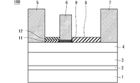
- the present disclosure has been made to solve the above problems, and aims to provide a nitride semiconductor device capable of suppressing the source starvation effect.
- FIG. 1 is a cross-sectional view schematically showing the configuration of a semiconductor device 100 according to Embodiment 1.
- the semiconductor device 100 is a nitride semiconductor HEMT.
- a semiconductor device 100 includes a substrate 1, a buffer layer 2, a first nitride semiconductor layer 3, a second nitride semiconductor layer 4, a source electrode 5, a gate electrode 6, a drain electrode 7, a protective It comprises a membrane 8 , a first oxide layer 11 and a second oxide layer 12 .
Landscapes
- Junction Field-Effect Transistors (AREA)
- Insulated Gate Type Field-Effect Transistor (AREA)
Abstract
Description
図1は、実施の形態1に係る半導体装置100の構成を模式的に示す断面図である。半導体装置100は、窒化物半導体HEMTである。図1に示すように、半導体装置100は、基板1、バッファ層2、第1の窒化物半導体層3、第2の窒化物半導体層4、ソース電極5、ゲート電極6、ドレイン電極7、保護膜8、第1の酸化物層11および第2の酸化物層12を備える。
図4は、実施の形態2に係る半導体装置200の構成を模式的に示す断面図である。半導体装置200も、窒化物半導体HEMTである。図4の半導体装置200の構成は、図1に示した半導体装置100の構成に対し、第2の酸化物層12の上方に、第3の酸化物層13、第4の酸化物層14および第5の酸化物層15を追加したものである。第1の酸化物層11および第2の酸化物層12と同様に、第3の酸化物層13、第4の酸化物層14および第5の酸化物層15も、ゲート電極6とソース電極5との間に配置される。
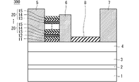
図6は、実施の形態3に係る半導体装置300の構成を模式的に示す断面図である。半導体装置300も、窒化物半導体HEMTである。図6の半導体装置200の構成は、図4に示した半導体装置200の構成に対し、第3の酸化物層13、第4の酸化物層14および第5の酸化物層15から構成される積層構造20を、第2の酸化物層12の上方に周期的に積み重ねたものである。以下、第3の酸化物層13、第4の酸化物層14および第5の酸化物層15から構成される積層構造20を「単位積層構造」という。
Claims (10)
- 第1の窒化物半導体層と、
前記第1の窒化物半導体層の上方に設けられ、前記第1の窒化物半導体層との間で二次元電子ガスを形成する第2の窒化物半導体層と、
前記第2の窒化物半導体層の上方に設けられ、前記二次元電子ガスと電気的に接続したソース電極と、
前記第2の窒化物半導体層の上方に設けられ、前記二次元電子ガスと電気的に接続したドレイン電極と、
前記第2の窒化物半導体層の上方に設けられ、前記ソース電極と前記ドレイン電極との間に配置されたゲート電極と、
前記第2の窒化物半導体層の上方に設けられ、前記ゲート電極と前記ドレイン電極との間に配置された保護膜と、
前記第2の窒化物半導体層の上方に設けられ、前記ゲート電極と前記ソース電極との間に配置された第1の酸化物層と、
前記第1の酸化物層の上方に設けられた第2の酸化物層と、
を備える半導体装置。 - 前記第1の酸化物層と前記第2の酸化物層との間の接合界面において、前記第1の酸化物層の酸素面密度は、前記第2の酸化物層の酸素面密度より低い、
請求項1に記載の半導体装置。 - 前記第1の酸化物層および前記第2の酸化物層は、いずれも非晶質である、
請求項1または請求項2に記載の半導体装置。 - 前記第1の酸化物層は、窒素を含有する、
請求項1から請求項3のいずれか一項に記載の半導体装置。 - 前記第2の酸化物層の上方に設けられた第3の酸化物層と、
前記第3の酸化物層の上方に設けられた第4の酸化物層と、
前記第4の酸化物層の上方に設けられた第5の酸化物層と、
をさらに備える、
請求項1から請求項4のいずれか一項に記載の半導体装置。 - 前記第2の酸化物層と前記第3の酸化物層との接合界面において、前記第2の酸化物層の酸素面密度は、前記第3の酸化物層の酸素面密度より高く、
前記第3の酸化物層と前記第4の酸化物層との接合界面において、前記第3の酸化物層の酸素面密度は、前記第4の酸化物層の酸素面密度より低く、
前記第4の酸化物層と前記第5の酸化物層との接合界面において、前記第4の酸化物層の酸素面密度は、前記第5の酸化物層の酸素面密度より低い、
請求項5に記載の半導体装置。 - 前記第3の酸化物層、前記第4の酸化物層および前記第5の酸化物層が、いずれも非晶質である、
請求項5または請求項6に記載の半導体装置。 - 前記第3の酸化物層、前記第4の酸化物層および前記第5の酸化物層から構成される単位積層構造が、前記第2の酸化物層の上方に周期的に形成されている、
請求項5から請求項7のいずれか一項に記載の半導体装置。 - 請求項1から請求項4のいずれか一項に記載の半導体装置の製造方法であって、
前記第1の酸化物層および前記第2の酸化物層を形成する工程と、
前記第1の酸化物層および前記第2の酸化物層が結晶化しない温度範囲で熱処理を行う工程と、
を備える半導体装置の製造方法。 - 請求項5から請求項8のいずれか一項に記載の半導体装置の製造方法であって、
前記第1の酸化物層、前記第2の酸化物層、前記第3の酸化物層、前記第4の酸化物層および前記第5の酸化物層を形成する工程と、
前記第1の酸化物層、前記第2の酸化物層、前記第3の酸化物層、前記第4の酸化物層および前記第5の酸化物層が結晶化しない温度範囲で熱処理を行う工程と、
を備える半導体装置の製造方法。
Priority Applications (5)
| Application Number | Priority Date | Filing Date | Title |
|---|---|---|---|
| CN202180099164.2A CN117461141A (zh) | 2021-06-14 | 2021-06-14 | 半导体装置及半导体装置的制造方法 |
| US18/567,796 US20240266429A1 (en) | 2021-06-14 | 2021-06-14 | Semiconductor device and method of manufacturing semiconductor device |
| DE112021007834.8T DE112021007834T5 (de) | 2021-06-14 | 2021-06-14 | Halbleitereinrichtung und verfahren zum herstellen der halbleitereinrichtung |
| PCT/JP2021/022442 WO2022264191A1 (ja) | 2021-06-14 | 2021-06-14 | 半導体装置および半導体装置の製造方法 |
| JP2021569573A JP7023438B1 (ja) | 2021-06-14 | 2021-06-14 | 半導体装置および半導体装置の製造方法 |
Applications Claiming Priority (1)
| Application Number | Priority Date | Filing Date | Title |
|---|---|---|---|
| PCT/JP2021/022442 WO2022264191A1 (ja) | 2021-06-14 | 2021-06-14 | 半導体装置および半導体装置の製造方法 |
Publications (1)
| Publication Number | Publication Date |
|---|---|
| WO2022264191A1 true WO2022264191A1 (ja) | 2022-12-22 |
Family
ID=81076737
Family Applications (1)
| Application Number | Title | Priority Date | Filing Date |
|---|---|---|---|
| PCT/JP2021/022442 Ceased WO2022264191A1 (ja) | 2021-06-14 | 2021-06-14 | 半導体装置および半導体装置の製造方法 |
Country Status (5)
| Country | Link |
|---|---|
| US (1) | US20240266429A1 (ja) |
| JP (1) | JP7023438B1 (ja) |
| CN (1) | CN117461141A (ja) |
| DE (1) | DE112021007834T5 (ja) |
| WO (1) | WO2022264191A1 (ja) |
Citations (4)
| Publication number | Priority date | Publication date | Assignee | Title |
|---|---|---|---|---|
| JP2014183125A (ja) * | 2013-03-18 | 2014-09-29 | Fujitsu Ltd | 半導体装置 |
| JP2014229767A (ja) * | 2013-05-23 | 2014-12-08 | 三菱電機株式会社 | ヘテロ接合電界効果型トランジスタ及びその製造方法 |
| JP2018117114A (ja) * | 2017-01-17 | 2018-07-26 | 株式会社東芝 | 半導体装置、電源回路、コンピュータ、及び、半導体装置の製造方法 |
| JP2019075550A (ja) * | 2017-10-16 | 2019-05-16 | 株式会社東芝 | 半導体装置および電気装置 |
Family Cites Families (6)
| Publication number | Priority date | Publication date | Assignee | Title |
|---|---|---|---|---|
| JP2007173426A (ja) * | 2005-12-21 | 2007-07-05 | Toshiba Corp | 半導体装置 |
| JP2014045174A (ja) * | 2012-08-01 | 2014-03-13 | Sharp Corp | 窒化物半導体装置 |
| CN104299999B (zh) * | 2014-10-11 | 2018-01-12 | 电子科技大学 | 一种具有复合栅介质层的氮化镓基异质结场效应晶体管 |
| US9954092B2 (en) * | 2016-07-22 | 2018-04-24 | Kabushiki Kaisha Toshiba | Semiconductor device, power circuit, and computer |
| JP2019050232A (ja) | 2017-09-07 | 2019-03-28 | ルネサスエレクトロニクス株式会社 | 半導体装置の製造方法および半導体装置 |
| WO2021024502A1 (ja) * | 2019-08-06 | 2021-02-11 | 三菱電機株式会社 | 半導体装置およびその製造方法 |
-
2021
- 2021-06-14 CN CN202180099164.2A patent/CN117461141A/zh active Pending
- 2021-06-14 DE DE112021007834.8T patent/DE112021007834T5/de active Pending
- 2021-06-14 JP JP2021569573A patent/JP7023438B1/ja active Active
- 2021-06-14 US US18/567,796 patent/US20240266429A1/en active Pending
- 2021-06-14 WO PCT/JP2021/022442 patent/WO2022264191A1/ja not_active Ceased
Patent Citations (4)
| Publication number | Priority date | Publication date | Assignee | Title |
|---|---|---|---|---|
| JP2014183125A (ja) * | 2013-03-18 | 2014-09-29 | Fujitsu Ltd | 半導体装置 |
| JP2014229767A (ja) * | 2013-05-23 | 2014-12-08 | 三菱電機株式会社 | ヘテロ接合電界効果型トランジスタ及びその製造方法 |
| JP2018117114A (ja) * | 2017-01-17 | 2018-07-26 | 株式会社東芝 | 半導体装置、電源回路、コンピュータ、及び、半導体装置の製造方法 |
| JP2019075550A (ja) * | 2017-10-16 | 2019-05-16 | 株式会社東芝 | 半導体装置および電気装置 |
Also Published As
| Publication number | Publication date |
|---|---|
| DE112021007834T5 (de) | 2024-04-04 |
| JP7023438B1 (ja) | 2022-02-21 |
| CN117461141A (zh) | 2024-01-26 |
| JPWO2022264191A1 (ja) | 2022-12-22 |
| US20240266429A1 (en) | 2024-08-08 |
Similar Documents
| Publication | Publication Date | Title |
|---|---|---|
| CN108321198B (zh) | 半导体装置、电源电路、计算机和半导体装置的制造方法 | |
| US8907349B2 (en) | Semiconductor device and method of manufacturing the same | |
| CN104009075B (zh) | 半导体装置 | |
| US8710550B2 (en) | Semiconductor device with hetero-junction bodies | |
| CN1943035B (zh) | GaN系半导体装置 | |
| CN106024879B (zh) | 半导体器件和制造半导体器件的方法 | |
| CN107731902B (zh) | 第iii族氮化物常关晶体管的层结构 | |
| US8759876B2 (en) | Enhancement-mode nitride transistor | |
| CN102239550A (zh) | 场效应晶体管 | |
| JP5534661B2 (ja) | 半導体装置 | |
| TW201528503A (zh) | 半導體裝置 | |
| TW201546992A (zh) | 半導體裝置 | |
| JPWO2011118098A1 (ja) | 電界効果トランジスタ、電界効果トランジスタの製造方法、および電子装置 | |
| JP2011210750A (ja) | 電界効果トランジスタ、電界効果トランジスタの製造方法、および電子装置 | |
| JP5997234B2 (ja) | 半導体装置、電界効果トランジスタおよび電子装置 | |
| CN108735811B (zh) | 半导体装置、电源电路以及计算机 | |
| WO2010016564A1 (ja) | 半導体装置 | |
| JP2013232578A (ja) | ショットキーバリアダイオード | |
| JP2014241379A (ja) | 半導体装置 | |
| JP5100002B2 (ja) | 窒化物半導体装置 | |
| JP7023438B1 (ja) | 半導体装置および半導体装置の製造方法 | |
| JP4850423B2 (ja) | 窒化物半導体装置 | |
| JP5208439B2 (ja) | 窒化物半導体装置 | |
| JP2008098674A (ja) | 半導体装置 | |
| CN121014277A (zh) | 半导体装置及半导体装置的制造方法 |
Legal Events
| Date | Code | Title | Description |
|---|---|---|---|
| ENP | Entry into the national phase |
Ref document number: 2021569573 Country of ref document: JP Kind code of ref document: A |
|
| 121 | Ep: the epo has been informed by wipo that ep was designated in this application |
Ref document number: 21945871 Country of ref document: EP Kind code of ref document: A1 |
|
| WWE | Wipo information: entry into national phase |
Ref document number: 202180099164.2 Country of ref document: CN |
|
| WWE | Wipo information: entry into national phase |
Ref document number: 112021007834 Country of ref document: DE |
|
| 122 | Ep: pct application non-entry in european phase |
Ref document number: 21945871 Country of ref document: EP Kind code of ref document: A1 |