WO2022259900A1 - フィルムコンデンサ - Google Patents
フィルムコンデンサ Download PDFInfo
- Publication number
- WO2022259900A1 WO2022259900A1 PCT/JP2022/022001 JP2022022001W WO2022259900A1 WO 2022259900 A1 WO2022259900 A1 WO 2022259900A1 JP 2022022001 W JP2022022001 W JP 2022022001W WO 2022259900 A1 WO2022259900 A1 WO 2022259900A1
- Authority
- WO
- WIPO (PCT)
- Prior art keywords
- electrode
- electrodes
- divided
- lateral direction
- small
- Prior art date
- Legal status (The legal status is an assumption and is not a legal conclusion. Google has not performed a legal analysis and makes no representation as to the accuracy of the status listed.)
- Ceased
Links
Images




Classifications
-
- H—ELECTRICITY
- H01—ELECTRIC ELEMENTS
- H01G—CAPACITORS; CAPACITORS, RECTIFIERS, DETECTORS, SWITCHING DEVICES, LIGHT-SENSITIVE OR TEMPERATURE-SENSITIVE DEVICES OF THE ELECTROLYTIC TYPE
- H01G4/00—Fixed capacitors; Processes of their manufacture
- H01G4/32—Wound capacitors
-
- H—ELECTRICITY
- H01—ELECTRIC ELEMENTS
- H01G—CAPACITORS; CAPACITORS, RECTIFIERS, DETECTORS, SWITCHING DEVICES, LIGHT-SENSITIVE OR TEMPERATURE-SENSITIVE DEVICES OF THE ELECTROLYTIC TYPE
- H01G4/00—Fixed capacitors; Processes of their manufacture
- H01G4/40—Structural combinations of fixed capacitors with other electric elements, the structure mainly consisting of a capacitor, e.g. RC combinations
Definitions
- the present disclosure generally relates to film capacitors, and more particularly relates to film capacitors used in electronic equipment, electrical equipment, industrial equipment, automobiles, and the like.
- Patent Document 1 discloses a film capacitor. This film capacitor employs a structure in which two capacitors are connected in series.
- the film capacitor of Patent Document 1 is a film capacitor having a structure in which two films are stacked and wound into a cylindrical shape.
- a partial electrode that is divided into two in the film width direction and divided into a plurality of parts in the winding direction is vapor-deposited.
- a plurality of sets of two partial electrodes arranged in the film width direction are connected to each other via a security mechanism positioned between the two partial electrodes for each set.
- Patent Literature 1 has the problem that it is not possible to alleviate the sudden concentration of current at the time of dielectric breakdown. Concentration of current increases the risk of penetrating breakdown.
- An object of the present disclosure is to provide a film capacitor that can reduce the risk of through breakdown even if dielectric breakdown occurs.
- a film capacitor according to an aspect of the present disclosure includes a dielectric film having a first surface and a second surface opposite to the first surface and extending in a longitudinal direction orthogonal to a lateral direction; It comprises a first electrode arranged on one surface and a second electrode arranged on the second surface.
- the film capacitor includes two unit capacitors connected in series in the lateral direction by facing the first electrode and the second electrode via the dielectric film.
- the first electrode is separated into two large split electrodes by the first margin extending in the longitudinal direction.
- Each of the two large split electrodes is divided into a plurality of partial electrodes aligned in the longitudinal direction by a first lateral direction slit extending in the lateral direction.
- the second electrode is a sub-divided electrode, and end margin portions extending in the longitudinal direction are present on both sides of the sub-divided electrode in the lateral direction.
- the sub-divided electrodes are divided into a plurality of sub-electrode groups aligned in the longitudinal direction by second lateral direction slit portions extending in the lateral direction.
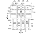
- FIG. 1 is an explanatory diagram showing the film capacitor according to the first embodiment.
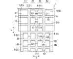
- FIG. 2 is an explanatory diagram showing a film capacitor according to the second embodiment.
- FIG. 3 is an explanatory diagram showing a film capacitor according to the third embodiment.
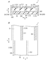
- FIG. 4 is a schematic cross-sectional view showing a film capacitor according to a fourth embodiment.
- FIG. 5 is an explanatory diagram showing the film capacitor same as the above.
- FIG. 6 is an explanatory diagram showing a film capacitor according to the fifth embodiment.
- FIG. 7A is a schematic cross-sectional view showing a film capacitor including one unit capacitor in the width direction.
- FIG. 7B is an explanatory diagram showing the same film capacitor.
- FIG. 8A is a schematic cross-sectional view showing a film capacitor including two unit capacitors connected in series in the width direction.
- FIG. 8B is an explanatory diagram showing the same film capacitor.
- FIG. 9A is a schematic cross-sectional view showing a film capacitor including three unit capacitors connected in series in the width direction.
- FIG. 9B is an explanatory diagram showing the same film capacitor.
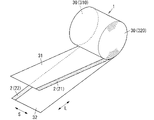
- FIG. 10 is a schematic perspective view showing an example of a film capacitor.
- FIG. 10 shows an example of a film capacitor 1 .
- the film capacitor 1 has, for example, a cylindrical shape.
- the film capacitor 1 is formed, for example, by stacking and winding two elongated dielectric films 2 (a first dielectric film 21 and a second dielectric film 22).
- the first electrode 31 is arranged on one side of the first dielectric film 21 .
- a second electrode 32 is arranged on one side of the second dielectric film 22 .
- the first electrode 31 and the second electrode 32 face each other with the dielectric film 2 interposed therebetween.
- Edge electrodes 30 (a first edge electrode 310 and a second edge electrode 320) are formed at both ends of the film capacitor 1 .
- the first electrode 31 is connected to the first edge electrode 310 .
- the second electrode 32 is connected to the second edge electrode 320 .
- the film capacitor 1 can include one to three unit capacitors 10 in the lateral direction S (width direction) of the dielectric film 2 (see FIGS. 7A, 8A and 9A). This point will be described below.
- one side of the transversal direction S may be called “left side” and the other side may be called “right side.”
- the film capacitor 1 shown in FIG. 7A includes one unit capacitor 10 in the lateral direction S of the dielectric film 2.
- FIG. 7A shows one unit capacitor 10 in the lateral direction S of the dielectric film 2.
- a first edge margin portion 241 is arranged on the right edge of one side of the first dielectric film 21 .
- the first electrode 31 is arranged on the entire one side of the first dielectric film 21 except for the first end margin portion 241 .
- the first electrode 31 includes the left end portion of one side of the first dielectric film 21 and is connected to the first edge electrode 310 at this portion (see FIG. 7A).
- the presence of the first edge margin portion 241 separates the first electrode 31 and the second edge electrode 320 from each other.
- a second edge margin portion 242 is arranged at the left edge of one side of the second dielectric film 22 .
- a second electrode 32 is arranged on the entire one side of the second dielectric film 22 excluding the second end margin portion 242 .
- the second electrode 32 includes the right edge of one side of the second dielectric film 22 and is connected to the second edge electrode 320 at this portion (see FIG. 7A).
- the presence of the second end margin portion 242 separates the second electrode 32 from the first end face electrode 310 .
- one unit capacitor 10 is formed in a portion where the first electrode 31 and the second electrode 32 face each other with the dielectric film 2 (first dielectric film 21) interposed therebetween.
- the film capacitor 1 shown in FIG. 8A includes two unit capacitors 10 connected in series in the transverse direction S of the dielectric film 2 .
- the first electrode 31 is divided into left and right sides by a first margin portion 211 .
- the left first electrode 31 includes the left end portion of one side of the first dielectric film 21 and is connected to the first edge electrode 310 at this portion.
- the right first electrode 31 includes the right end portion of one side of the first dielectric film 21 and is connected to the second edge electrode 320 at this portion (see FIG. 8A).
- second edge margin portions 242 are arranged at the left edge and right edge of one side of the second dielectric film 22 .
- the second electrode 32 is arranged entirely between the second end margin portions 242 on both sides. The presence of the second edge margin portions 242 on both sides separates the second electrode 32 from the first edge electrode 310 and the second edge electrode 320 .
- two unit capacitors 10 are formed in the portion where the first electrode 31 and the second electrode 32 face each other with the dielectric film 2 (first dielectric film 21) interposed therebetween. These unit capacitors 10 are connected in series in the lateral direction S. As shown in FIG. 8A, two unit capacitors 10 are formed in the portion where the first electrode 31 and the second electrode 32 face each other with the dielectric film 2 (first dielectric film 21) interposed therebetween. These unit capacitors 10 are connected in series in the lateral direction S. As shown in FIG.
- the film capacitor 1 shown in FIG. 9A includes three unit capacitors 10 connected in series in the transverse direction S of the dielectric film 2 .
- the first electrode 31 is divided into left and right sides by a first margin portion 211 .
- the left first electrode 31 includes the left edge of one side of the first dielectric film 21 and is connected to the first edge electrode 310 at this portion (see FIG. 9A).
- a first edge margin portion 241 is arranged at the right edge of one side of the first dielectric film 21 .
- the first electrode 31 on the right side is arranged entirely between the first margin portion 211 and the first end margin portion 241 .
- the presence of the first end margin portion 241 separates the right first electrode 31 and the second end face electrode 320 from each other.
- the second electrode 32 is divided into left and right sides by the second margin portion 212 .
- the right second electrode 32 includes the right edge of one side of the second dielectric film 22 and is connected to the second edge electrode 320 at this portion (see FIG. 9A).
- a second edge margin portion 242 is arranged at the left edge of one side of the second dielectric film 22 .
- the left second electrode 32 is disposed entirely between the second end margin portion 242 and the second margin portion 212 . The presence of the second edge margin portion 242 separates the left second electrode 32 from the first edge electrode 310 .
- FIG. 9A three unit capacitors 10 are formed in portions where the first electrode 31 and the second electrode 32 face each other with the dielectric film 2 (first dielectric film 21) interposed therebetween. These unit capacitors 10 are connected in series in the lateral direction S. As shown in FIG. 9A, three unit capacitors 10 are formed in portions where the first electrode 31 and the second electrode 32 face each other with the dielectric film 2 (first dielectric film 21) interposed therebetween. These unit capacitors 10 are connected in series in the lateral direction S. As shown in FIG.
- the voltage applied to the film capacitors 1 shown in FIGS. 7A, 8A and 9A is the same, the voltage applied to the unit capacitor 10 of the film capacitor 1 shown in FIG. 9A is By making it the smallest, it becomes easier to suppress damage to the dielectric film 2 .
- the present inventor further improved the film capacitor 1 in which a plurality of unit capacitors 10 are connected in series in the lateral direction S, and developed the following film capacitor 1.
- the first electrode 31 is separated into two large split electrodes 7 by the first margin portion 211 .
- Each of the two large split electrodes 7 is split into a plurality of partial electrodes 710 by the first transverse direction slit portions 221 .
- the second electrode 32 is the sub-divided electrode 8 .
- End margin portions 242 are present on both sides of the sub-divided electrode 8 in the lateral direction S.
- the sub-divided electrode 8 is divided into a plurality of sub-electrode groups 520 by the second lateral direction slit portions 222 .
- Small electrode group 520 includes a plurality of small electrodes 521 .
- the first unit capacitor 10 is formed in the portion (Z1 portion in FIG. 1) where the large divided electrode 7 on the left and the small electrode 521 on the left face each other with the dielectric film 2 interposed therebetween.
- a second unit capacitor 10 is formed in a portion (Z2 portion in FIG. 1) where the right large divided electrode 7 and the right small electrode 521 face each other with the dielectric film 2 interposed therebetween.
- each of the two large split electrodes 7 of the first electrode 31 is split into a plurality of partial electrodes 710, and the small split electrodes 8 of the second electrode 32 are also split into a plurality of small electrode groups 520. Since it is divided, even if a dielectric breakdown occurs in a certain portion (for example, point P in FIG. 1) between the first electrode 31 and the second electrode 32, the other portion (point P in FIG. 1) can be transferred to the portion where the dielectric breakdown occurred. Inflow of current from Q) can be suppressed by the first transverse direction slit portion 221 and the second transverse direction slit portion 222 .
- the film capacitor 1 according to this embodiment may be of the wound type or the laminated type.
- dielectric breakdown means a phenomenon in which when a voltage is applied to the dielectric film 2, the applied voltage cannot be maintained.
- Through-hole breakdown means a full-path breakdown that occurs not through the surface of the dielectric film 2 but through the inside.
- the film capacitor 1 includes a dielectric film 2, a first electrode 31 and a second electrode 32.
- the first electrode 31 and the second electrode 32 face each other with the dielectric film 2 (in this embodiment, the first dielectric film 21) interposed therebetween, and are connected in series in the lateral direction S. It contains two unit capacitors 10 (see FIG. 8A).
- the dielectric film 2, the first electrode 31, and the second electrode 32 will be described below.
- the dielectric film 2 is a film made of a dielectric.
- the dielectric is not particularly limited, but examples thereof include polypropylene (PP) and polyethylene terephthalate (PET).
- the dielectric film 2 has an elongated film shape. That is, the dielectric film 2 is a film extending in the longitudinal direction L orthogonal to the lateral direction S. As shown in FIG.
- the dielectric film 2 has a first surface 201 and a second surface 202 (see FIG. 8A).
- the first surface 201 is a surface facing one side in the thickness direction T of the dielectric film 2 .
- a thickness direction T is a direction orthogonal to the lateral direction S and the longitudinal direction L.
- the second surface 202 is the surface opposite to the first surface 201 . That is, the second surface 202 is a surface facing the other side in the thickness direction T of the dielectric film 2 .
- the dielectric film 2 includes a first dielectric film 21 and a second dielectric film 22.
- the first electrode 31 may be any of a vapor deposition electrode, a metal foil electrode, and a plated electrode.
- the material of the first electrode 31 is not particularly limited, but examples thereof include aluminum.
- the first electrode 31 is arranged on the first surface 201 of the dielectric film 2 (the first dielectric film 21 in this embodiment).
- the first electrode 31 is separated into two large split electrodes 7 by a first margin portion 211 .
- the first margin portion 211 is a portion of the first surface 201 of the first dielectric film 21 where the first electrode 31 is not arranged. Therefore, the dielectric film 2 is exposed at this portion.
- the first margin portion 211 extends in the longitudinal direction L with a constant width.
- One of the two large split electrodes 7 is an electrode arranged on one side (left side) in the transverse direction S.
- the other of the two large split electrodes 7 is an electrode arranged on the other side (right side) in the transverse direction S. As shown in FIG.
- Each of the two large split electrodes 7 is split into a plurality of partial electrodes 710 by at least one or more first transverse direction slits 221 .
- the first transverse direction slit portion 221 is a portion of the first surface 201 of the first dielectric film 21 where the first electrode 31 is not arranged. Accordingly, the dielectric film 2 is exposed in this portion as well as in the first margin portion 211 .
- the first lateral direction slit portion 221 extends in the lateral direction S with a constant width.
- the first transverse direction slit portion 221 is connected to one (left) end and the other (right) end of the first dielectric film 21 in the transverse direction S. As shown in FIG. Therefore, the first transverse direction slit portion 221 crosses the first margin portion 211 .
- the width of the first lateral direction slit portion 221 is the same as the width of the first margin portion 211, but may be different within a range that does not impair the effects of the present embodiment.
- the plurality of partial electrodes 710 are arranged in the longitudinal direction L.
- the shape of the partial electrode 710 is rectangular, but is not particularly limited.
- the sizes of the plurality of partial electrodes 710 are the same in this embodiment, they may be different as long as the effects of this embodiment are not impaired.
- the second electrode 32 may also be any of a vapor deposition electrode, a metal foil electrode, and a plated electrode.
- the material of the second electrode 32 is also the same as the material of the first electrode 31 .
- the second electrode 32 is arranged on the second surface 202 of the dielectric film 2 (the first dielectric film 21 in this embodiment). In other words, the second electrode 32 is arranged on the first surface 201 of the second dielectric film 22 in this embodiment.
- the second electrode 32 is the subdivided electrode 8 .
- End margin portions 242 are present on both sides of the sub-divided electrode 8 in the lateral direction S. As shown in FIG.
- the end margin portions 242 are present at one (left) end and the other (right) end in the transverse direction S of the second dielectric film 22 .
- the end margin portion 242 is a portion where the second electrode 32 is not arranged. Therefore, the dielectric film 2 is exposed at this portion.
- the end margin portion 242 extends in the longitudinal direction L with a constant width. The existence of the end margin portion 242 allows the second electrode 32 (the sub-divided electrode 8) to be separated from the first end surface electrode 310 and the second end surface electrode 320 .
- sub-divided electrode 8 is divided into a plurality of sub-electrode groups 520 by at least one or more second lateral direction slits 222 .
- the second lateral direction slit portion 222 is a portion of the first surface 201 of the second dielectric film 22 where the second electrode 32 is not arranged. Accordingly, the dielectric film 2 is exposed in this portion as well as in the edge margin portion 242 .
- the second transverse direction slit portion 222 extends in the transverse direction S with a constant width.
- the second lateral direction slit portion 222 is connected to the left and right end margin portions 242 .
- the width of the second lateral direction slit portion 222 is the same as the width of the end margin portion 242, but may be different within a range that does not impair the effects of the present embodiment.
- the width of the second transverse direction slit portion 222 is the same as the width of the first transverse direction slit portion 221, but may differ within a range that does not impair the effects of the present embodiment.
- the plurality of small electrode groups 520 are arranged in the longitudinal direction L.
- the small electrode group 520 includes a plurality of (two in this embodiment) small electrodes 521 .
- the plurality of small electrodes 521 are arranged in the lateral direction S.
- the shape of the small electrodes 521 is rectangular, but is not particularly limited.
- the sizes of the plurality of small electrodes 521 are the same in this embodiment, they may be different as long as the effects of this embodiment are not impaired.
- a plurality of small electrodes 521 included in each of the plurality of small electrode groups 520 are connected by fuses 62 .
- the fuse 62 is a part that melts and cuts off the circuit when an excessive current flows.
- the fuse 62 connects the small electrodes 521 adjacent to each other in the lateral direction S. As shown in FIG.
- the width of the fuse 62 is shorter than the length of the small electrode 521 in the longitudinal direction L.
- the second electrode 32 described above faces the first electrode 31 via the dielectric film 2 (the first dielectric film 21 in this embodiment).
- the second electrode 32 (the small segmented electrode 8) faces the large segmented electrode 7 on the left side of the first electrode 31 through the dielectric film 2.
- the left small electrode 521 of the second electrode 32 faces the left partial electrode 710 of the first electrode 31 with the dielectric film 2 interposed therebetween.
- a first unit capacitor 10 is formed in this portion.
- the film capacitor 1 includes a plurality of unit capacitor groups (one unit capacitor group is a portion C surrounded by a dashed line in FIG. 1).
- a plurality of unit capacitor groups are arranged in the longitudinal direction L.
- Each of the plurality of unit capacitor groups is connected to the facet electrode 30 (the first facet electrode 310 and the second facet electrode 320). That is, a plurality of unit capacitor groups are connected in parallel.
- Each unit capacitor group includes two unit capacitors 10 connected in series in the transverse direction S. As shown in FIG.
- ⁇ Effect> For example, as shown in FIG. 8, when a dielectric breakdown occurs at point P, a current can flow from around point P toward point P. In FIG. Assuming that a point around point P is point Q, current can flow from point Q toward point P along a straight path. As a result, dielectric breakdown may lead to penetration breakdown immediately.
- the first electrode 31 is a solid electrode extending in the longitudinal direction L.
- the partial electrode 710 where the point P exists and the partial electrode 710 where the point Q exists are separated by the first lateral direction slit portion 221 .
- the first electrode 31 is divided in the longitudinal direction L into a plurality of parts.
- each of the two large split electrodes 7 of the first electrode 31 is split into a plurality of partial electrodes 710, and the small split electrodes 8 of the second electrode 32 are also split into a plurality of small electrodes. Since it is divided into the electrode group 520, even if a dielectric breakdown occurs in a certain portion between the first electrode 31 and the second electrode 32, it is possible to prevent current from flowing into this dielectrically broken portion from other portions. It can be suppressed by the first lateral direction slit portion 221 and the second lateral direction slit portion 222 .
- the film capacitor 1 according to this embodiment differs from the first embodiment shown in FIG. Although it is common to the film capacitor 1, it differs from the film capacitor 1 according to the first embodiment in that the number of unit capacitors 10 connected in series in the lateral direction S is three.
- the first electrode 31 and the second electrode 32 face each other with the dielectric film 2 (in this embodiment, the first dielectric film 21) interposed therebetween.
- S includes three unit capacitors 10 connected in series (see FIG. 9A).
- the first electrode 31 is separated into a first large segmented electrode 71 and a first small segmented electrode 81 by a first margin portion 211 .
- the first large split electrode 71 is arranged between the first margin portion 211 and the end portion of the first dielectric film 21 on one side (left side) in the transverse direction S.
- the first large split electrode 71 is split into a plurality of first partial electrodes 710 by at least one or more first lateral direction slit portions 221 .
- the first lateral direction slit portion 221 is connected to one side (left side) of the first dielectric film 21 in the lateral direction S and the first margin portion 211 .
- the plurality of first partial electrodes 710 are arranged in the longitudinal direction L.
- the left end of each of the plurality of first partial electrodes 710 can be connected to the first end face electrode 310 (not shown in FIG. 2).
- the first sub-divided electrode 81 is arranged between the first margin portion 211 and the first end margin portion 241 .
- the first end margin portion 241 exists at the end of the first dielectric film 21 on the other side (right side) in the transverse direction S. Similarly to the first margin portion 211, the first end margin portion 241 is also a portion where the first electrode 31 is not arranged. Therefore, the dielectric film 2 is also exposed in this portion.
- the first end margin portion 241 extends in the longitudinal direction L with a constant width. The presence of the first edge margin portion 241 allows the first sub-divided electrode 81 and the second edge electrode 320 (not shown in FIG. 2) to be separated from each other.
- the width of the first end margin portion 241 is the same as the width of the first margin portion 211, but may be different within a range that does not impair the effects of the present embodiment.
- the first sub-divided electrode 81 is divided into a plurality of first sub-electrode groups 510 by at least one or more first lateral direction slits 221 .
- the first lateral direction slit portion 221 is connected to the first margin portion 211 and the first end margin portion 241 .
- the plurality of first small electrode groups 510 are arranged in the longitudinal direction L.
- the first small electrode group 510 is aligned in the lateral direction S with the first partial electrodes 710 .
- the first small electrode group 510 includes a plurality of (two in this embodiment) first small electrodes 511 .
- the plurality of first small electrodes 511 are arranged in the lateral direction S. As shown in FIG.
- the shape of the first small electrode 511 is rectangular, but is not particularly limited. Also, in this embodiment, the sizes of the plurality of first small electrodes 511 are the same, but they may be different as long as the effects of this embodiment are not impaired.
- a plurality of first small electrodes 511 included in each of the plurality of first small electrode groups 510 are connected by a first fuse 61 .
- the first fuse 61 like the fuse 62 of the first embodiment, is a portion that melts when an excessive current flows to cut off the circuit.
- the first fuse 61 connects the first small electrodes 511 adjacent in the lateral direction S to each other.
- the width of the first fuse 61 is shorter than the length in the longitudinal direction L of the first small electrode 511 .
- the second electrode 32 is separated by a second margin portion 212 into a second large segmented electrode 72 and a second small segmented electrode 82 .
- the second margin portion 212 is a portion of the first surface 201 of the second dielectric film 22 where the second electrode 32 is not arranged. Therefore, the dielectric film 2 is exposed at this portion.
- the second margin portion 212 extends in the longitudinal direction L with a constant width.
- the width of the second margin portion 212 is the same as the width of the first margin portion 211, but may be different within a range that does not impair the effects of the present embodiment.
- the second large split electrode 72 is arranged between the second margin portion 212 and the other (right) end of the second dielectric film 22 in the transverse direction S.
- the second large split electrode 72 is split into a plurality of second partial electrodes 720 by second lateral direction slits 222 .
- the second lateral direction slit portion 222 is connected to one side (right side) of the second dielectric film 22 in the lateral direction S and the second margin portion 212 .
- the plurality of second partial electrodes 720 are arranged in the longitudinal direction L.
- the right end of each of the plurality of second partial electrodes 720 can be connected to the second end face electrode 320 (not shown in FIG. 2).
- the second sub-divided electrode 82 is arranged between the second margin portion 212 and the second end margin portion 242 .
- the second edge margin portion 242 exists at one side (left side) edge in the transverse direction S of the second dielectric film 22 .
- the presence of the second edge margin portion 242 allows the second sub-divided electrode 82 and the first edge electrode 310 (not shown in FIG. 2) to be separated from each other.
- the width of the second end margin portion 242 is the same as the width of the second margin portion 212, but may be different within a range that does not impair the effects of the present embodiment.
- the second sub-divided electrode 82 is divided into a plurality of second sub-electrode groups 520 by at least one or more second lateral direction slits 222 .
- the plurality of second small electrode groups 520 are arranged in the longitudinal direction L.
- the second small electrode group 520 is aligned in the lateral direction S with the second partial electrodes 720 .
- the second small electrode group 520 includes a plurality of (two in this embodiment) second small electrodes 521 .
- the plurality of second small electrodes 521 are arranged in the lateral direction S. As shown in FIG. In this embodiment, the shape of the second small electrode 521 is rectangular, but is not particularly limited. In addition, although the sizes of the plurality of second small electrodes 521 are the same in this embodiment, they may be different as long as the effects of this embodiment are not impaired.
- a plurality of second small electrodes 521 included in each of the plurality of second small electrode groups 520 are connected by a second fuse 62 .
- the second fuse 62 like the first fuse 61, is a portion that melts when an excessive current flows to cut off the circuit.
- the second fuse 62 connects the second small electrodes 521 adjacent to each other in the lateral direction S. As shown in FIG.
- the width of the second fuse 62 is shorter than the length in the longitudinal direction L of the second small electrode 521 .
- the second electrode 32 described above faces the first electrode 31 via the dielectric film 2 (the first dielectric film 21 in this embodiment).
- a film capacitor 1 according to the present embodiment also includes a plurality of unit capacitor groups (a portion C surrounded by a dashed line in FIG. 2 is one unit capacitor group) as in the first embodiment.
- a plurality of unit capacitor groups are arranged in the longitudinal direction L.
- Each of the plurality of unit capacitor groups is connected to the edge electrode 30 (the first edge electrode 310 and the second edge electrode 320). That is, a plurality of unit capacitor groups are connected in parallel.
- each unit capacitor group in this embodiment includes three unit capacitors 10 connected in series in the lateral direction S. As shown in FIG.
- the film capacitor 1 according to this embodiment includes three unit capacitors 10 connected in series in the transverse direction S of the dielectric film 2, like the film capacitor 1 shown in FIG. 9A. Therefore, the voltage applied between the first end surface electrode 310 and the second end surface electrode 320 of the film capacitor 1 shown in FIGS. 7A and 8A and the first end surface electrode 310 and the second end surface of the film capacitor 1 according to the present embodiment
- the voltage applied between the electrodes 320 is the same
- the voltage applied to the unit capacitor 10 of the film capacitor 1 according to the present embodiment is higher than the voltage applied to the unit capacitor 10 of the film capacitor 1 shown in FIGS. 7A and 8A. By reducing the applied voltage, it becomes easier to suppress damage to the dielectric film 2 .
- the plurality of first small electrodes 511 are connected by the first fuse 61
- the plurality of second small electrodes 521 are connected by the second fuse. 62 are connected. Therefore, even if a part between the first electrode 31 and the second electrode 32 is short-circuited, at least one of the first fuse 61 and the second fuse 62 is disconnected.
- the film capacitor 1 according to the present embodiment includes three unit capacitors 10 connected in series in the transverse direction S. , but differs from the film capacitor 1 according to the second embodiment in that a first connection portion 91 and a second connection portion 92 are further present.
- the description will focus on the differences from the second embodiment.
- the first connection portion 91 is present at one side (left side) end in the transverse direction S of the dielectric film 2 (first dielectric film 21).
- the first connecting portion 91 exists between the first partial electrodes 710 adjacent to each other in the longitudinal direction L. As shown in FIG. In this manner, the plurality of first partial electrodes 710 are connected by the first connecting portion 91 .
- the first connecting portion 91 has conductivity. Therefore, the first connecting portion 91 may be formed as part of the first electrode 31 . That is, the first connection portion 91 may be any of a vapor deposition electrode, a metal foil electrode, and a plated electrode.
- the material of the first connecting portion 91 is not particularly limited, but examples thereof include aluminum.
- the length of the first connecting portion 91 is shorter than the length of the first partial electrode 710 in the lateral direction S of the dielectric film 2 (first dielectric film 21). Therefore, between the first partial electrodes 710 adjacent in the longitudinal direction L, the first connecting portion 91 and the first transverse direction slit portion 221 are present.
- the second connection portion 92 is present at the other (right) end in the transverse direction S of the dielectric film 2 (second dielectric film 22).
- the second connection portion 92 exists between the second partial electrodes 720 adjacent to each other in the longitudinal direction L. As shown in FIG. In this manner, the plurality of second partial electrodes 720 are connected by the second connecting portion 92 .
- the second connection part 92 has conductivity, like the first connection part 91 . Therefore, the second connection portion 92 may be formed as part of the second electrode 32 . That is, like the first connection portion 91, the second connection portion 92 may be any of a vapor deposition electrode, a metal foil electrode, and a plated electrode. The material of the second connection portion 92 is also the same as the material of the first connection portion 91 .
- the length of the second connecting portion 92 is shorter than the length of the second partial electrode 720 in the lateral direction S of the dielectric film 2 (second dielectric film 22). Therefore, between the second partial electrodes 720 adjacent to each other in the longitudinal direction L, the second connecting portion 92 and the second lateral direction slit portion 222 are present.
- a film capacitor 1 according to this embodiment also includes a plurality of unit capacitor groups, as in the second embodiment.
- a plurality of unit capacitor groups are arranged in the longitudinal direction L.
- Each of the plurality of unit capacitor groups is connected to the facet electrode 30 (the first facet electrode 310 and the second facet electrode 320). That is, a plurality of unit capacitor groups are connected in parallel.
- Each unit capacitor group includes three unit capacitors 10 connected in series in the transverse direction S. As shown in FIG. However, the plurality of unit capacitor groups in this embodiment are connected by the first connection portion 91 and the second connection portion 92 .
- a plurality of first partial electrodes are connected by the first connecting portion 91 and a plurality of second partial electrodes are connected by the second connecting portion 92 . That is, a plurality of unit capacitor groups are connected by the first connection portion 91 and the second connection portion 92 .
- a film capacitor 1 according to a fourth embodiment will be described with reference to the drawings.
- the same reference numerals as in the first to third embodiments may be assigned to the same components as in the first to third embodiments, and detailed description thereof may be omitted.
- the film capacitor 1 according to this embodiment is common to the film capacitors 1 according to the second and third embodiments in that it includes three unit capacitors 10 connected in series in the transverse direction S, but the film capacitor 1 according to the transverse direction S is different from the film capacitors 1 according to the first to third embodiments in that it can include four or more unit capacitors 10 connected in series.
- the film capacitor 1 according to this embodiment is obtained by expanding or generalizing the number of unit capacitors 10 connected in series in the lateral direction S to three or more.
- the number of unit capacitors 10 connected in series in the lateral direction S is assumed to be n (where n is an integer of 3 or more).
- the film capacitor 1 includes a portion (Z1 and Z4 portions) where the first large segmented electrode 71 and the second small segmented electrode 82 face each other with the dielectric film 2 interposed therebetween; There are portions (Z2 and Z3 portions) facing the sub-divided electrodes 82 .
- the dielectric film 2 of this embodiment is the same as the dielectric films 2 of the first to third embodiments.
- the first electrode 31 is separated by at least one or more first margin portions 211 into at least one or more first large segmented electrodes 71 and at least one or more first small segmented electrodes 81 .
- the first electrodes 31 are separated into (n+1)/2 pieces.
- the first electrode 31 is separated into one first large segmented electrode 71 and one first small segmented electrode 81 by one first margin portion 211 .
- the first electrode 31 is connected to the first edge electrode 310 but not to the second edge electrode 320 .
- the first large split electrode 71 arranged on one side (left side) in the short direction S of the dielectric film 2 is connected to the first end surface electrode 310.
- the first sub-divided electrode 81 arranged on the other side (right side) of the dielectric film 2 in the transverse direction S is not connected to the second end surface electrode 320 .
- the first electrode 31 is separated by at least two or more first margin portions 211 into at least two or more first large segmented electrodes 71 and at least one or more first small segmented electrodes 81 .
- the first electrodes 31 are separated into (n+2)/2 pieces.
- the first electrode 31 is separated into three (see FIGS. 4 and 5).
- the first electrode 31 is separated into two first large split electrodes 71 and one first small split electrode 81 by two first margin portions 211 .
- the first electrode 31 is connected to the first edge electrode 310 and the second edge electrode 320 .
- the first large segmented electrode 71 arranged on one side (left side) in the short direction S of the dielectric film 2 is connected to the first end surface electrode 310
- the first large split electrode 71 arranged on the other side (right side) of the dielectric film 2 in the transverse direction S is connected to the second end surface electrode 320 .
- the first large segmented electrode 71 is preferably connected to the end face electrode 30 .
- the first small electrode group 510 includes a plurality of (two in this embodiment) first small electrodes 511 (see FIGS. 2 and 5). A plurality of first small electrodes 511 are connected by a first fuse 61 .
- the second electrode 32 is separated into at least one or more second large segmented electrodes 72 and at least one or more second small segmented electrodes 82 by at least one or more second margin portions 212 .
- the second electrodes 32 are separated into (n+1)/2 pieces.
- the second electrode 32 is separated into one second large segmented electrode 72 and one second small segmented electrode 82 by one second margin portion 212 .
- the second electrode 32 is not connected to the first edge electrode 310 but is connected to the second edge electrode 320 .
- the second sub-divided electrode 82 arranged on one side (left side) in the transverse direction S of the dielectric film 2 is not connected to the first end surface electrode 310, but the dielectric
- the second large split electrode 72 arranged on the other side (right side) of the body film 2 in the transverse direction S is connected to the second edge electrode 320 .
- the second electrode 32 is separated into at least two or more second sub-divided electrodes 82 by at least one or more second margin portions 212 .
- the second electrodes 32 are separated into n/2 pieces.
- the second electrode 32 is separated into two (see FIGS. 4 and 5).
- the second electrode 32 is separated into two second sub-divided electrodes 82 by one second margin 212 .
- the second electrode 32 is not connected to the first edge electrode 310 and the second edge electrode 320 .
- the second sub-divided electrode 82 arranged on one side (left side) in the transverse direction S of the dielectric film 2 is not connected to the first end face electrode 310 and is not connected to the dielectric film 2.
- the second sub-divided electrode 82 arranged on the other side (right side) of the body film 2 in the transverse direction S is also not connected to the second edge electrode 320 .
- the second electrode 32 includes a second large split electrode 72
- the second large split electrode 72 is preferably connected to the edge electrode 30 .
- the second small electrode group 520 includes a plurality of (two in this embodiment) second small electrodes 521 (see FIGS. 2 and 5). A plurality of second small electrodes 521 are connected by a second fuse 62 .
- the film capacitor 1 according to the present embodiment also includes a plurality of unit capacitor groups (one unit capacitor group is a portion C surrounded by a dashed line in FIGS. 2 and 5), as in the first to third embodiments.
- a plurality of unit capacitor groups are arranged in the longitudinal direction L.
- Each of the plurality of unit capacitor groups is connected to the facet electrode 30 (the first facet electrode 310 and the second facet electrode 320). That is, a plurality of unit capacitor groups are connected in parallel.
- each unit capacitor group of the present embodiment includes three or more unit capacitors 10 connected in series in the lateral direction S. As shown in FIG.
- each unit capacitor group includes three or more unit capacitors 10 connected in series in the transverse direction S. As the number of unit capacitors 10 included in each unit capacitor group increases, the voltage applied to each unit capacitor 10 decreases. Therefore, damage to the dielectric film 2 can be easily suppressed.
- a film capacitor 1 according to a fifth embodiment will be described with reference to the drawings.
- the same reference numerals as in the first to fourth embodiments may be assigned to the same components as in the first to fourth embodiments, and detailed description thereof may be omitted.
- the film capacitor 1 according to the present embodiment includes three or more unit capacitors 10 connected in series in the lateral direction S in common with the film capacitor 1 according to the fourth embodiment.
- the first connection portion 91 and the second connection portion 92 are further present. It is different from the film capacitor 1 according to the fourth embodiment in one point (see FIG. 3).
- the first connection portion 91 is further present (see FIG. 6). ), which is different from the film capacitor 1 according to the fourth embodiment.
- One first large split electrode 71 out of at least one or more first large split electrodes 71 is present on one side (left side) in the transverse direction S of the dielectric film 2 (first dielectric film 21). .
- first dielectric film 21 first dielectric film 21
- the plurality of first partial electrodes 710 are connected by a first connecting portion 91 present at the left end portion in the lateral direction S. As shown in FIG.
- Two first large split electrodes 71 out of at least two or more first large split electrodes 71 are arranged on one side (left side) and the other side in the transverse direction S of the dielectric film 2 (first dielectric film 21). (on the right).
- first dielectric film 21 first dielectric film 21
- second dielectric film 21 first dielectric film 21
- a plurality of first partial electrodes 710 of the first large segmented electrode 71 arranged on the left side in the lateral direction S are connected by a first connecting portion 91 present at the left end portion of the dielectric film 2 .
- the plurality of first partial electrodes 710 of the first large segmented electrode 71 arranged on the right side in the lateral direction S are connected by a first connecting portion 91 present at the right end portion of the dielectric film 2 .
- ⁇ Second electrode> [When n is an odd number of 3 or more] One second large segmented electrode 72 out of at least one or more second large segmented electrodes 72 is present on the other side (right side) in the transverse direction S of the dielectric film 2 (second dielectric film 22). .
- n 3
- the plurality of second partial electrodes 720 are connected by a second connecting portion 92 present at the right end portion in the lateral direction S. As shown in FIG.
- a film capacitor 1 according to this embodiment also includes a plurality of unit capacitor groups, as in the fourth embodiment.
- a plurality of unit capacitor groups are arranged in the longitudinal direction L.
- Each of the plurality of unit capacitor groups is connected to the facet electrode 30 (the first facet electrode 310 and the second facet electrode 320). That is, a plurality of unit capacitor groups are connected in parallel.
- Each unit capacitor group includes three or more unit capacitors 10 connected in series in the transverse direction S.
- the plurality of unit capacitor groups consist of the first connecting portion 91 and the second connecting portion 92 are connected by (see FIG. 3).
- the plurality of unit capacitor groups are connected by the first connecting portion 91. (See Figure 6).
Landscapes
- Engineering & Computer Science (AREA)
- Power Engineering (AREA)
- Manufacturing & Machinery (AREA)
- Microelectronics & Electronic Packaging (AREA)
- Fixed Capacitors And Capacitor Manufacturing Machines (AREA)
Priority Applications (2)
| Application Number | Priority Date | Filing Date | Title |
|---|---|---|---|
| JP2023527622A JP7850993B2 (ja) | 2021-06-11 | 2022-05-30 | フィルムコンデンサ |
| CN202280040133.4A CN117461103A (zh) | 2021-06-11 | 2022-05-30 | 薄膜电容器 |
Applications Claiming Priority (2)
| Application Number | Priority Date | Filing Date | Title |
|---|---|---|---|
| JP2021-098312 | 2021-06-11 | ||
| JP2021098312 | 2021-06-11 |
Publications (1)
| Publication Number | Publication Date |
|---|---|
| WO2022259900A1 true WO2022259900A1 (ja) | 2022-12-15 |
Family
ID=84424927
Family Applications (1)
| Application Number | Title | Priority Date | Filing Date |
|---|---|---|---|
| PCT/JP2022/022001 Ceased WO2022259900A1 (ja) | 2021-06-11 | 2022-05-30 | フィルムコンデンサ |
Country Status (3)
| Country | Link |
|---|---|
| JP (1) | JP7850993B2 (https=) |
| CN (1) | CN117461103A (https=) |
| WO (1) | WO2022259900A1 (https=) |
Citations (7)
| Publication number | Priority date | Publication date | Assignee | Title |
|---|---|---|---|---|
| JPH0272609A (ja) * | 1988-09-07 | 1990-03-12 | Marcon Electron Co Ltd | Shコンデンサ |
| JPH0357206A (ja) * | 1989-07-26 | 1991-03-12 | Nichicon Corp | エネルギー蓄積急放電用コンデンサ |
| JPH03104724U (https=) * | 1990-02-14 | 1991-10-30 | ||
| JPH06168844A (ja) * | 1992-04-06 | 1994-06-14 | Nichicon Corp | 電力用高圧コンデンサ |
| JPH0757955A (ja) * | 1993-08-09 | 1995-03-03 | Shizuki Denki Seisakusho:Kk | 金属化フィルムコンデンサ |
| JPH07240336A (ja) * | 1994-08-29 | 1995-09-12 | Nichicon Corp | 電力用高圧コンデンサ |
| JP2012191045A (ja) * | 2011-03-11 | 2012-10-04 | Nichicon Corp | 電力用高圧コンデンサ素子、および当該素子を用いた電力用高圧コンデンサ |
-
2022
- 2022-05-30 WO PCT/JP2022/022001 patent/WO2022259900A1/ja not_active Ceased
- 2022-05-30 JP JP2023527622A patent/JP7850993B2/ja active Active
- 2022-05-30 CN CN202280040133.4A patent/CN117461103A/zh active Pending
Patent Citations (7)
| Publication number | Priority date | Publication date | Assignee | Title |
|---|---|---|---|---|
| JPH0272609A (ja) * | 1988-09-07 | 1990-03-12 | Marcon Electron Co Ltd | Shコンデンサ |
| JPH0357206A (ja) * | 1989-07-26 | 1991-03-12 | Nichicon Corp | エネルギー蓄積急放電用コンデンサ |
| JPH03104724U (https=) * | 1990-02-14 | 1991-10-30 | ||
| JPH06168844A (ja) * | 1992-04-06 | 1994-06-14 | Nichicon Corp | 電力用高圧コンデンサ |
| JPH0757955A (ja) * | 1993-08-09 | 1995-03-03 | Shizuki Denki Seisakusho:Kk | 金属化フィルムコンデンサ |
| JPH07240336A (ja) * | 1994-08-29 | 1995-09-12 | Nichicon Corp | 電力用高圧コンデンサ |
| JP2012191045A (ja) * | 2011-03-11 | 2012-10-04 | Nichicon Corp | 電力用高圧コンデンサ素子、および当該素子を用いた電力用高圧コンデンサ |
Also Published As
| Publication number | Publication date |
|---|---|
| JP7850993B2 (ja) | 2026-04-24 |
| JPWO2022259900A1 (https=) | 2022-12-15 |
| CN117461103A (zh) | 2024-01-26 |
Similar Documents
| Publication | Publication Date | Title |
|---|---|---|
| US9536663B2 (en) | Metallized film capacitor | |
| JP4698474B2 (ja) | フィルムコンデンサ | |
| US7164184B2 (en) | Multilayer capacitor | |
| US20110013341A1 (en) | Multilayer chip capacitor | |
| JP5548343B2 (ja) | 金属化フィルムコンデンサ | |
| JP2010016047A (ja) | 金属化フィルムコンデンサ | |
| WO2022259900A1 (ja) | フィルムコンデンサ | |
| US9779877B2 (en) | Film capacitor | |
| JP5294123B2 (ja) | 金属化フィルムコンデンサ | |
| JP2016207823A (ja) | フィルムコンデンサ素子 | |
| JP7296734B2 (ja) | 金属化フィルム及び金属化フィルムコンデンサ | |
| JP6330139B2 (ja) | 金属化フィルムコンデンサ | |
| JPH06267786A (ja) | コンデンサ | |
| JP7850992B2 (ja) | フィルムコンデンサ | |
| US9570239B2 (en) | Electrode forming film and film capacitor using the same | |
| CN111448631A (zh) | 薄膜电容器 | |
| JP6614558B2 (ja) | 金属化フィルム及び金属化フィルムコンデンサ | |
| JP2017143170A (ja) | 金属化フィルムとこの金属化フィルムを用いた金属化フィルムコンデンサ | |
| JP2010087260A (ja) | 積層コンデンサ | |
| KR100809238B1 (ko) | 적층형 칩 커패시터 | |
| JP2006032904A (ja) | 積層型セラミックキャパシタ | |
| JP7850994B2 (ja) | フィルムコンデンサ | |
| JP6040592B2 (ja) | 金属化フィルムコンデンサ | |
| WO2024171702A1 (ja) | コンデンサ | |
| JP2002353060A (ja) | 金属化フィルムコンデンサ |
Legal Events
| Date | Code | Title | Description |
|---|---|---|---|
| 121 | Ep: the epo has been informed by wipo that ep was designated in this application |
Ref document number: 22820082 Country of ref document: EP Kind code of ref document: A1 |
|
| WWE | Wipo information: entry into national phase |
Ref document number: 2023527622 Country of ref document: JP |
|
| WWE | Wipo information: entry into national phase |
Ref document number: 202280040133.4 Country of ref document: CN |
|
| NENP | Non-entry into the national phase |
Ref country code: DE |
|
| 122 | Ep: pct application non-entry in european phase |
Ref document number: 22820082 Country of ref document: EP Kind code of ref document: A1 |