WO2022255128A1 - 多層基板、多層基板の製造方法及び電子機器 - Google Patents
多層基板、多層基板の製造方法及び電子機器 Download PDFInfo
- Publication number
- WO2022255128A1 WO2022255128A1 PCT/JP2022/020959 JP2022020959W WO2022255128A1 WO 2022255128 A1 WO2022255128 A1 WO 2022255128A1 JP 2022020959 W JP2022020959 W JP 2022020959W WO 2022255128 A1 WO2022255128 A1 WO 2022255128A1
- Authority
- WO
- WIPO (PCT)
- Prior art keywords
- interlayer connection
- conductor
- layer
- connection conductor
- main surface
- Prior art date
- Legal status (The legal status is an assumption and is not a legal conclusion. Google has not performed a legal analysis and makes no representation as to the accuracy of the status listed.)
- Ceased
Links
Images







Classifications
-
- H—ELECTRICITY
- H01—ELECTRIC ELEMENTS
- H01P—WAVEGUIDES; RESONATORS, LINES, OR OTHER DEVICES OF THE WAVEGUIDE TYPE
- H01P3/00—Waveguides; Transmission lines of the waveguide type
- H01P3/02—Waveguides; Transmission lines of the waveguide type with two longitudinal conductors
- H01P3/08—Microstrips; Strip lines
- H01P3/085—Triplate lines
-
- H—ELECTRICITY
- H01—ELECTRIC ELEMENTS
- H01P—WAVEGUIDES; RESONATORS, LINES, OR OTHER DEVICES OF THE WAVEGUIDE TYPE
- H01P3/00—Waveguides; Transmission lines of the waveguide type
- H01P3/02—Waveguides; Transmission lines of the waveguide type with two longitudinal conductors
- H01P3/08—Microstrips; Strip lines
-
- H—ELECTRICITY
- H01—ELECTRIC ELEMENTS
- H01P—WAVEGUIDES; RESONATORS, LINES, OR OTHER DEVICES OF THE WAVEGUIDE TYPE
- H01P11/00—Apparatus or processes specially adapted for manufacturing waveguides or resonators, lines, or other devices of the waveguide type
- H01P11/001—Manufacturing waveguides or transmission lines of the waveguide type
- H01P11/003—Manufacturing lines with conductors on a substrate, e.g. strip lines, slot lines
-
- H—ELECTRICITY
- H05—ELECTRIC TECHNIQUES NOT OTHERWISE PROVIDED FOR
- H05K—PRINTED CIRCUITS; CASINGS OR CONSTRUCTIONAL DETAILS OF ELECTRIC APPARATUS; MANUFACTURE OF ASSEMBLAGES OF ELECTRICAL COMPONENTS
- H05K1/00—Printed circuits
- H05K1/02—Details
-
- H—ELECTRICITY
- H05—ELECTRIC TECHNIQUES NOT OTHERWISE PROVIDED FOR
- H05K—PRINTED CIRCUITS; CASINGS OR CONSTRUCTIONAL DETAILS OF ELECTRIC APPARATUS; MANUFACTURE OF ASSEMBLAGES OF ELECTRICAL COMPONENTS
- H05K1/00—Printed circuits
- H05K1/02—Details
- H05K1/0213—Electrical arrangements not otherwise provided for
- H05K1/0216—Reduction of cross-talk, noise or electromagnetic interference
- H05K1/0218—Reduction of cross-talk, noise or electromagnetic interference by printed shielding conductors, ground planes or power plane
- H05K1/0219—Printed shielding conductors for shielding around or between signal conductors, e.g. coplanar or coaxial printed shielding conductors
-
- H—ELECTRICITY
- H05—ELECTRIC TECHNIQUES NOT OTHERWISE PROVIDED FOR
- H05K—PRINTED CIRCUITS; CASINGS OR CONSTRUCTIONAL DETAILS OF ELECTRIC APPARATUS; MANUFACTURE OF ASSEMBLAGES OF ELECTRICAL COMPONENTS
- H05K3/00—Apparatus or processes for manufacturing printed circuits
- H05K3/46—Manufacturing multilayer circuits
-
- H—ELECTRICITY
- H05—ELECTRIC TECHNIQUES NOT OTHERWISE PROVIDED FOR
- H05K—PRINTED CIRCUITS; CASINGS OR CONSTRUCTIONAL DETAILS OF ELECTRIC APPARATUS; MANUFACTURE OF ASSEMBLAGES OF ELECTRICAL COMPONENTS
- H05K2201/00—Indexing scheme relating to printed circuits covered by H05K1/00
- H05K2201/09—Shape and layout
- H05K2201/09209—Shape and layout details of conductors
- H05K2201/095—Conductive through-holes or vias
- H05K2201/09509—Blind vias, i.e. vias having one side closed
- H05K2201/09527—Inverse blind vias, i.e. bottoms outwards in multilayer PCB; Blind vias in centre of PCB having opposed bottoms
-
- H—ELECTRICITY
- H05—ELECTRIC TECHNIQUES NOT OTHERWISE PROVIDED FOR
- H05K—PRINTED CIRCUITS; CASINGS OR CONSTRUCTIONAL DETAILS OF ELECTRIC APPARATUS; MANUFACTURE OF ASSEMBLAGES OF ELECTRICAL COMPONENTS
- H05K2201/00—Indexing scheme relating to printed circuits covered by H05K1/00
- H05K2201/09—Shape and layout
- H05K2201/09209—Shape and layout details of conductors
- H05K2201/095—Conductive through-holes or vias
- H05K2201/096—Vertically aligned vias, holes or stacked vias
-
- H—ELECTRICITY
- H05—ELECTRIC TECHNIQUES NOT OTHERWISE PROVIDED FOR
- H05K—PRINTED CIRCUITS; CASINGS OR CONSTRUCTIONAL DETAILS OF ELECTRIC APPARATUS; MANUFACTURE OF ASSEMBLAGES OF ELECTRICAL COMPONENTS
- H05K2201/00—Indexing scheme relating to printed circuits covered by H05K1/00
- H05K2201/09—Shape and layout
- H05K2201/09209—Shape and layout details of conductors
- H05K2201/095—Conductive through-holes or vias
- H05K2201/09609—Via grid, i.e. two-dimensional array of vias or holes in a single plane
Definitions
- the present invention relates to a multilayer substrate having a structure in which a plurality of insulator layers are laminated.
- This multilayer substrate includes a laminate, a first ground conductor, a second ground conductor, a first interlayer connection conductor, and a second interlayer connection conductor.
- the laminate has a structure in which a plurality of insulating base materials are laminated vertically.
- the first ground conductor is provided on the upper main surface of the insulating base.
- the second ground conductor is provided on the lower main surface of the insulating base.
- the first interlayer connection conductor and the second interlayer connection conductor vertically penetrate the insulating base material.
- the upper end of the first interlayer connection conductor and the upper end of the second interlayer connection conductor are connected to the first ground conductor.
- a lower end of the first interlayer connection conductor and a lower end of the second interlayer connection conductor are connected to the second ground conductor.
- an object of the present invention is to electrically connect a plurality of interlayer connection conductors and one or more first metal foil layers, and to electrically connect a plurality of interlayer connection conductors and one or more second metal foil layers. It is an object of the present invention to provide a multilayer board, a method for manufacturing the multilayer board, and an electronic device capable of suppressing the occurrence of connection failures.
- a multilayer substrate comprises It has a structure in which a plurality of insulating layers including a first insulating layer having a first main surface and a second main surface are laminated so as to be aligned in a first direction, and the first main surface is the a laminate positioned in the first direction from the second main surface; a plurality of interlayer connection conductors penetrating the first insulator layer in the first direction, the plurality of interlayer connection conductors including a first interlayer connection conductor and a second interlayer connection conductor; in contact with the first main surface of the first insulator layer, in contact with the first interlayer connection conductor and the second interlayer connection conductor, and having a third main surface and a fourth main surface; wherein the third main surface is positioned in the first direction from the fourth main surface, and the composition of the first conductor layer is the composition of the first interlayer connection conductor and a first conductor layer having the same composition as the second interlayer connection conductor; one or more first metal foil
- a method for manufacturing a multilayer substrate comprises: a third insulator layer having a ninth principal surface and a tenth principal surface, a first insulator layer having a first principal surface and a second principal surface, and a seventh principal surface and an eighth principal surface;
- the method for manufacturing the multilayer substrate comprises: a first preparation step of preparing the first insulator layer provided with a first through hole and a second through hole; a second preparation step of preparing the second insulator layer having the first metal foil layer provided on the eighth main surface; a third preparation step of preparing the third insulator layer having the second metal
- the electrical connection between the plurality of interlayer connection conductors and the one or more first metal foil layers and the electrical connection between the plurality of interlayer connection conductors and the one or more second metal foil layers It is possible to suppress the occurrence of defective connections.
- FIG. 1 is an exploded perspective view of a multilayer substrate 10.
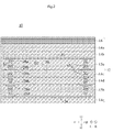
- FIG. FIG. 2 is a cross-sectional view along AA in FIG.
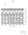
- FIG. 3 is a cross-sectional view along BB in FIG.
- FIG. 4 is a diagram showing a part of the electronic device 100.
- FIG. 5 is a cross-sectional view of the multilayer substrate 10 during manufacture.
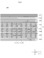
- FIG. 6 is a cross-sectional view of the multilayer substrate 10a.
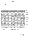
- FIG. 7 is a cross-sectional view of the multilayer substrate 10b.
- FIG. 8 is a cross-sectional view of the multilayer substrate 10c.
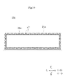
- FIG. 9 is a top view of the insulator layer 15a of the multilayer substrate 10d.
- FIG. 10 is a top view of the insulator layer 15a of the multilayer substrate 10e.
- FIG. 11 is a perspective view of the multilayer substrate 10f from above.
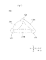
- FIG. 12 is a bottom view of the insulator layer 15a of the multilayer substrate 10g.
- FIG. 13 is a cross-sectional view perpendicular to the vertical direction of the insulator layer 15a of the multilayer substrate 10h.
- FIG. 1 is an exploded perspective view of a multilayer substrate 10.
- FIG. 1 only representative interlayer connection conductors v7 among the plurality of interlayer connection conductors v7 are denoted by reference numerals.
- FIG. 2 is a cross-sectional view along AA in FIG.
- FIG. 3 is a cross-sectional view along BB in FIG.
- FIG. 4 is a diagram showing a part of the electronic device 100. As shown in FIG.
- the vertical direction is defined as the direction in which the plurality of insulating layers 14a to 14e, 15a, and 15b are arranged.
- the upward or downward direction is the first direction.
- the second direction is opposite to the first direction. Therefore, if the upward direction is the first direction, the downward direction is the second direction. If the downward direction is the first direction, the upward direction is the second direction.
- the direction in which the first signal conductor layer 20 extends is defined as the horizontal direction.
- the horizontal direction is perpendicular to the vertical direction.
- a direction orthogonal to the left-right direction and the up-down direction is defined as the front-rear direction. Note that the vertical direction, the front-rear direction, and the left-right direction in the present embodiment do not have to match the vertical direction, the front-rear direction, and the left-right direction when the multilayer substrate 10 is used.
- X is a part or member of the multilayer substrate 10.
- each part of X is defined as follows.
- front of X is meant the front half of X.
- Back of X means the back half of X.
- the left part of X means the left half of X.
- the right part of X means the right half of X.
- Top of X means the top half of X.
- the lower part of X means the lower half of X.
- the leading edge of X means the leading edge of X.
- the trailing end of X means the trailing end of X.
- the left end of X means the end of X in the left direction.
- the right end of X means the end of X in the right direction.
- the upper end of X means the end of X in the upward direction.
- the lower end of X means the lower end of X.
- the front end of X means the front end of X and its vicinity.
- the rear end of X means the rear end of X and its vicinity.
- the left end of X means the left end of X and its vicinity.
- the right end of X means the right end of X and its vicinity.
- the upper end of X means the upper end of X and its vicinity.
- the lower end of X means the lower end of X and its vicinity.
- the multilayer substrate 10 transmits high frequency signals.
- a multilayer substrate 10 is used to electrically connect two circuits in an electronic device such as a smart phone.
- the multilayer substrate 10 includes a laminate 12, a protective layer 16, a first signal conductor layer 20, a reference conductor layer 22 (second metal foil layer), and a reference conductor layer 24 (second metal foil layer).
- reference conductor layer 26a first metal foil layer
- reference conductor layer 26b first metal foil layer
- first conductor layers 28b, 28c second conductor layers 28a, 28d
- signal terminals 40, 50, reference terminal 42 , 44, 52, 54 interlayer connection conductors v1 to v6, and a plurality of interlayer connection conductors v7.
- the laminate 12 has a structure in which insulator layers 14a to 14e, 15a, and 15b (plurality of insulator layers) are stacked in a vertical direction (first direction).
- the plurality of insulator layers 14a, 14b, 15a, 14c, 14d, 15b, and 14e are arranged in this order from top to bottom.
- Each of the insulator layers 14a-14e has an upper major surface and a lower major surface.
- Each of the insulator layers 14a to 14e has a rectangular shape when viewed in the vertical direction. Long sides of the insulator layers 14a to 14e extend in the horizontal direction.
- the insulator layer 15a has an upper main surface (second main surface) and a lower main surface (first main surface).
- the lower main surface (first main surface) is positioned below (in the first direction) the upper main surface (second main surface).
- the insulator layer 15b has an upper main surface (first main surface) and a lower main surface (second main surface).
- the upper main surface (first main surface) is positioned above (in the first direction) the lower main surface (second main surface).
- Each of the insulator layers 15a and 15b has a rectangular shape when viewed in the vertical direction. Long sides of the insulator layers 15a and 15b extend in the horizontal direction.
- the insulator layers 14a to 14e, 15a and 15b contain thermoplastic resin.
- Thermoplastic resins are, for example, thermoplastic resins such as liquid crystal polymer and PTFE (polytetrafluoroethylene).
- the insulator layers 14a-14e, 15a, 15b may contain polyimide.
- the first conductor layer 28b is in contact with the lower main surface (first main surface) of the insulator layer 15a (first insulator layer).
- the first conductor layer 28b has an upper main surface (fourth main surface) and a lower main surface (third main surface).
- the lower main surface (third main surface) is positioned below (first direction) the upper main surface (fourth main surface).
- the first conductor layer 28b has a rectangular annular shape when viewed downward (first direction). More specifically, the first conductor layer 28b extends along two long sides and two short sides of the insulator layer 15a when viewed in the vertical direction.
- the second conductor layer 28a is in contact with the upper main surface (second main surface) of the insulator layer 15a (first insulator layer).
- the second conductor layer 28a has an upper main surface (sixth main surface) and a lower main surface (fifth main surface).
- the lower main surface (fifth main surface) is positioned below (first direction) the upper main surface (sixth main surface).
- the second conductor layer 28a has the same shape as the first conductor layer 28b when viewed in the vertical direction.
- the second conductor layer 28a has a rectangular ring shape when viewed in the vertical direction. More specifically, the second conductor layer 28a extends along two long sides and two short sides of the insulator layer 15a when viewed in the vertical direction.
- the entire outer edge of the second conductor layer 28a overlaps the entire outer edge of the first conductor layer 28b when viewed in the vertical direction.
- the entire inner edge of the second conductor layer 28a overlaps the entire inner edge of the first conductor layer 28b when viewed in the vertical direction.
- the reference conductor layer 26a is located on the upper main surface of the insulator layer 14c. Also, the first conductor layer 28b is located on the reference conductor layer 26a. Thereby, the reference conductor layer 26a (first metal foil layer) is in contact with the lower main surface (third main surface) of the first conductor layer 28b.
- the reference conductor layer 26a has a rectangular ring shape when viewed in the vertical direction. More specifically, the reference conductor layer 26a extends along two long sides and two short sides of the insulator layer 14c when viewed in the vertical direction. However, the outer edge of the reference conductor layer 26a is positioned slightly outside the outer edge of the first conductor layer 28b when viewed in the vertical direction. The inner edge of the reference conductor layer 26a is positioned slightly inside the inner edge of the first conductor layer 28b when viewed in the vertical direction.
- the reference conductor layer 22 is located on the lower main surface of the insulator layer 14b. Thereby, the reference conductor layer 22 is positioned above (second direction) the insulator layer 15a (first insulator layer). That is, the reference conductor layer 22 (second metal foil layer) is positioned above (second direction) the insulator layer 15a (first insulator layer). Also, the second conductor layer 28 a is located below the reference conductor layer 22 . Thereby, the reference conductor layer 22 (second metal foil layer) is in contact with the upper main surface (sixth main surface) of the second conductor layer 28a.
- the reference conductor layer 22 has a rectangular shape when viewed in the vertical direction.
- the reference conductor layer 22 covers substantially the entire lower main surface of the insulator layer 14b when viewed in the vertical direction. However, openings are provided in the reference conductor layer 22 at positions overlapping the interlayer connection conductors v1 and v2 when viewed in the vertical direction so that the reference conductor layer 22 does not come into contact with the interlayer connection conductors v1 and v2 described later.
- the first conductor layer 28c, the second conductor layer 28d, and the reference conductor layers 24, 26b have a vertically symmetrical structure with the first conductor layer 28b, the second conductor layer 28a, and the reference conductor layers 22, 26a. More specifically, the first conductor layer 28c is in contact with the upper main surface (first main surface) of the insulator layer 15b (first insulator layer).
- the first conductor layer 28c has an upper main surface (third main surface) and a lower main surface (fourth main surface). In the first conductor layer 28c, the upper main surface (third main surface) is located above (first direction) the lower main surface (fourth main surface).
- the first conductor layer 28c has a rectangular ring shape when viewed in the vertical direction (first direction). More specifically, the first conductor layer 28c extends along two long sides and two short sides of the insulator layer 14e when viewed in the vertical direction.
- the second conductor layer 28d is in contact with the lower main surface (second main surface) of the insulator layer 15b (first insulator layer).
- the second conductor layer 28d has an upper main surface (fifth main surface) and a lower main surface (sixth main surface).
- the upper main surface (fifth main surface) is located above (first direction) the lower main surface (sixth main surface).
- the second conductor layer 28d has the same shape as the first conductor layer 28c when viewed in the vertical direction.
- the second conductor layer 28d has a rectangular ring shape when viewed in the vertical direction (first direction).
- the second conductor layer 28d extends along two long sides and two short sides of the insulator layer 15b when viewed in the vertical direction.
- the entire outer edge of the second conductor layer 28d overlaps the entire outer edge of the first conductor layer 28c when viewed in the vertical direction.
- the entire inner edge of the second conductor layer 28d overlaps the entire inner edge of the first conductor layer 28c when viewed in the vertical direction.
- the reference conductor layer 26b is located on the lower main surface of the insulator layer 14d. Also, the first conductor layer 28c is located below the reference conductor layer 26b. Thereby, the reference conductor layer 26b (first metal foil layer) is in contact with the upper main surface (third main surface) of the first conductor layer 28c.
- the reference conductor layer 26b has a rectangular ring shape when viewed in the vertical direction. More specifically, the reference conductor layer 26b extends along two long sides and two short sides of the insulator layer 14d when viewed in the vertical direction. However, the outer edge of the reference conductor layer 26b is positioned slightly outside the outer edge of the first conductor layer 28c when viewed in the vertical direction. The inner edge of the reference conductor layer 26b is positioned slightly inside the inner edge of the first conductor layer 28c when viewed in the vertical direction.
- the reference conductor layer 24 is located on the upper main surface of the insulator layer 14e. Also, the second conductor layer 28 d is located on the reference conductor layer 24 . Thereby, the reference conductor layer 24 (second metal foil layer) is in contact with the lower main surface (sixth main surface) of the second conductor layer 28d.
- the reference conductor layer 24 has a rectangular shape when viewed in the vertical direction. More specifically, the reference conductor layer 24 covers substantially the entire upper major surface of the insulator layer 14e when viewed in the vertical direction.
- the reference conductor layers 22, 24, 26a, 26b as described above are connected to a reference potential.
- the reference potential is, for example, the ground potential.
- the plurality of interlayer connection conductors v7 penetrate the insulator layers 15a, 14c, 14d, and 15b in the vertical direction (first direction).
- the plurality of interlayer connection conductors v7 are arranged along the first conductor layers 28b, 28c and the second conductor layers 28a, 28d when viewed in the vertical direction.
- a plurality of interlayer connection conductors v7 are connected to the reference conductor layers 22, 24, 26a, 26b, the first conductor layers 28b, 28c, and the second conductor layers 28a, 28d.
- the multiple interlayer connection conductors v7 include multiple interlayer connection conductors v7a and multiple interlayer connection conductors v7b, as shown in FIG.
- the plurality of interlayer connection conductors v7a and the plurality of interlayer connection conductors v7b are arranged alternately.
- FIG. 3 only representative interlayer connection conductors v7a and interlayer connection conductors v7b among the plurality of interlayer connection conductors v7a and plurality of interlayer connection conductors v7b are denoted by reference numerals.
- the interlayer connection conductor v7a and the interlayer connection conductor v7b are adjacent to each other.
- the interlayer connection conductor v7b is the interlayer connection conductor located closest to the interlayer connection conductor v7a.
- the interlayer connection conductor v7a includes interlayer connection conductors v11 to v14.
- the interlayer connection conductors v11 to v14 have a circular shape when viewed in the vertical direction.
- the interlayer connection conductors v11 to v14 are arranged in a line in this order from top to bottom.
- the interlayer connection conductor v11 (first interlayer connection conductor) penetrates downward (first direction) through the insulator layer 15a (first insulator layer).
- the interlayer connection conductor v11 is connected to the second conductor layer 28a and the first conductor layer 28b.
- the diameter of the lower end of the interlayer connection conductor v11 is larger than the diameter of the upper end of the interlayer connection conductor v11.
- the interlayer connection conductor v12 penetrates downward through the insulator layer 14c.
- the interlayer connection conductor v12 is connected to the reference conductor layer 26a.
- the diameter of the lower end of the interlayer connection conductor v12 is larger than the diameter of the upper end of the interlayer connection conductor v12.
- the interlayer connection conductor v13 penetrates the insulator layer 14d upward.
- the interlayer connection conductor v13 is connected to the interlayer connection conductor v12 and the reference conductor layer 26b.
- the diameter of the upper end of the interlayer connection conductor v13 is larger than the diameter of the lower end of the interlayer connection conductor v13.
- the interlayer connection conductor v14 (first interlayer connection conductor) penetrates the insulator layer 15b (first insulator layer) upward (first direction).
- the interlayer connection conductor v14 is connected to the first conductor layer 28c and the second conductor layer 28d.
- the diameter of the upper end of the interlayer connection conductor v14 is larger than the diameter of the lower end of the interlayer connection conductor v14.
- the interlayer connection conductor v21 (second interlayer connection conductor) is the interlayer connection conductor located closest to the interlayer connection conductor v11 (first interlayer connection conductor).
- the interlayer connection conductor v7b includes interlayer connection conductors v21 to v24.
- the interlayer connection conductors v21 to v24 have a circular shape when viewed in the vertical direction.
- the interlayer connection conductors v21 to v24 are arranged in a line in this order from top to bottom.
- the interlayer connection conductor v21 (second interlayer connection conductor) penetrates downward (first direction) through the insulator layer 15a (first insulator layer).
- the interlayer connection conductor v21 is connected to the second conductor layer 28a and the first conductor layer 28b.
- the diameter of the lower end of the interlayer connection conductor v21 is larger than the diameter of the upper end of the interlayer connection conductor v21.
- the interlayer connection conductor v22 penetrates downward through the insulator layer 14c.
- the interlayer connection conductor v22 is connected to the reference conductor layer 26a.
- the diameter of the lower end of the interlayer connection conductor v22 is larger than the diameter of the upper end of the interlayer connection conductor v22.
- the interlayer connection conductor v23 penetrates the insulator layer 14d upward.
- the interlayer connection conductor v23 is connected to the interlayer connection conductor v22 and the reference conductor layer 26b.
- the diameter of the upper end of the interlayer connection conductor v23 is larger than the diameter of the lower end of the interlayer connection conductor v23.
- the interlayer connection conductor v24 (first interlayer connection conductor) penetrates the insulator layer 15b (first insulator layer) upward (first direction).
- the interlayer connection conductor v24 is connected to the first conductor layer 28c and the second conductor layer 28d.
- the diameter of the upper end of the interlayer connection conductor v24 is larger than the diameter of the lower end of the interlayer connection conductor v24.
- the interlayer connection conductor v24 (second interlayer connection conductor) is the interlayer connection conductor located closest to the interlayer connection conductor v14 (first interlayer connection conductor).
- the reference conductor layer 26a first metal foil layer
- the reference conductor layer 22 second metal foil layer
- the first conductor layer 28b and the second conductor layer 28a overlaps the interlayer connection conductor v11 (first interlayer connection conductor) and the interlayer connection conductor v21 (second interlayer connection conductor) when viewed downward (first direction).
- the reference conductor layer 26b first metal foil layer
- the reference conductor layer 26a second metal foil layer
- the first conductor layer 28b, and the second conductor layer 28a extend downward (first direction). As you can see, it overlaps with the interlayer connection conductor v11 (first interlayer connection conductor) and the interlayer connection conductor v21 (second interlayer connection conductor).
- the second conductor layer 28a is in contact with the interlayer connection conductor v11 (first interlayer connection conductor) and the interlayer connection conductor v21 (second interlayer connection conductor).
- the reference conductor layer 22 is in contact with the second conductor layer 28a. Therefore, the reference conductor layer 22 (second metal foil layer) is electrically connected to the interlayer connection conductor v11 (first interlayer connection conductor) and the interlayer connection conductor v21 (second interlayer connection conductor) through the second conductor layer 28a. It is connected to the.
- the first conductor layer 28b is in contact with the interlayer connection conductor v11 (first interlayer connection conductor) and the interlayer connection conductor v21 (second interlayer connection conductor).
- the reference conductor layer 26a is in contact with the first conductor layer 28b. Therefore, the reference conductor layer 26a is electrically connected to the interlayer connection conductor v11 (first interlayer connection conductor) and the interlayer connection conductor v21 (second interlayer connection conductor) through the first conductor layer 28b.
- the reference conductor layer 26b (first metal foil layer), the reference conductor layer 24 (second metal foil layer), the first conductor layer 28c, and the second conductor layer 28d are viewed upward (first direction), It overlaps with the interlayer connection conductor v14 (first interlayer connection conductor) and the interlayer connection conductor v24 (second interlayer connection conductor).
- the reference conductor layer 26b (first metal foil layer), the reference conductor layer 24 (second metal foil layer), the first conductor layer 28c, and the second conductor layer 28d are arranged upward (first direction). As you can see, it overlaps with the interlayer connection conductor v14 (first interlayer connection conductor) and the interlayer connection conductor v24 (second interlayer connection conductor).
- the first conductor layer 28c is in contact with the interlayer connection conductor v14 (first interlayer connection conductor) and the interlayer connection conductor v24 (second interlayer connection conductor).
- the reference conductor layer 26b is in contact with the first conductor layer 28c. Therefore, the reference conductor layer 26b (first metal foil layer) is electrically connected to the interlayer connection conductor v14 (first interlayer connection conductor) and the interlayer connection conductor v24 (second interlayer connection conductor) through the first conductor layer 28c. It is connected to the.
- the second conductor layer 28d is in contact with the interlayer connection conductor v14 (first interlayer connection conductor) and the interlayer connection conductor v24 (second interlayer connection conductor).
- the reference conductor layer 24 is in contact with the second conductor layer 28d. Therefore, the reference conductor layer 24c is electrically connected to the interlayer connection conductor v14 (first interlayer connection conductor) and the interlayer connection conductor v24 (second interlayer connection conductor) through the second conductor layer 28d.
- the interlayer connection conductors v11 to v14 and v21 to v24 as described above are formed by filling the through holes provided in the insulating layers 14b to 14d, 15a and 15b with a conductive paste and solidifying the conductive paste by heating. formed.
- the first conductor layers 28b, 28c and the second conductor layers 28a, 28d are formed by applying a conductive paste to the upper or lower main surfaces of the reference conductor layers 22, 26a, 26b, 24, and heating the conductive paste.
- the composition of the first conductor layers 28b and 28c and the composition of the second conductor layers 28a and 28d are the same as the composition of the interlayer connection conductors v11 and v14 (first interlayer connection conductors) and the interlayer connection conductors v21 and v24 (second interlayer connection conductors). interlayer connection conductor).
- the conductive paste contains resin and metal powder.
- the metal powder is, for example, an alloy powder of Sn and Cu.
- the interlayer connection conductors v11 and v14 (first interlayer connection conductors) and the interlayer connection conductors v21 and v24 (second interlayer connection conductors) contain resin and metal.
- "having the same composition” means "including the same alloy containing a plurality of metals.” Specifically, alloys of Sn and other metals, such as SuAgCu, are included.
- the reference conductor layers 22, 24, 26a and 26b are formed by etching metal foils provided on the upper or lower main surfaces of the insulator layers 14b, 14c, 14d and 14e. ing.
- the metal foil is, for example, copper foil.
- the compositions of the reference conductor layers 26a and 26b (first metal foil layers) and the reference conductor layers 22 and 24 (second metal foil layers) are the compositions of the first conductor layers 28b and 28c and the compositions of the second conductor layers 28a and 28d. different from
- a first high-frequency signal is transmitted to the first signal conductor layer 20 .
- the first high frequency signal is, for example, a digital signal.
- the first signal conductor layer 20 is located on the upper main surface of the insulator layer 14c, as shown in FIG.
- the first signal conductor layer 20 has a linear shape when viewed in the vertical direction.
- the first signal conductor layer 20 extends in the left-right direction.
- the first signal conductor layer 20 is surrounded by the first conductor layer 28b when viewed in the vertical direction (first direction).
- the first conductor layer 28b surrounds the first signal conductor layer 20, which is a circuit element that emits noise, when viewed in the vertical direction (first direction).
- the reference conductor layer 22 is located on the first signal conductor layer 20 .
- a reference conductor layer 24 is located below the first signal conductor layer 20 . Thereby, the first signal conductor layer 20 and the reference conductor layers 22 and 24 have a stripline structure.
- a plane passing through the center of the insulator layer 15a in the vertical direction is defined as a plane S1.
- the distance D1 between the interlayer connection conductor v11 (first interlayer connection conductor) and the interlayer connection conductor v21 (second interlayer connection conductor) and "the interlayer connection conductor v11 (first interlayer connection conductor) and the first The distance D2 from the signal conductor layer 20 is defined as follows.
- the shortest distance between the cross section of the interlayer connection conductor v11 (first interlayer connection conductor) on the plane S1 and the cross section of the interlayer connection conductor v21 (second interlayer connection conductor) on the plane S1 is defined as the distance D1.
- the shortest distance between the cross section of the interlayer connection conductor v11 (first interlayer connection conductor) on the plane S1 and the first signal conductor layer 20 when viewed in the vertical direction is defined as a distance D2.
- the distance D1 between the interlayer connection conductor v11 (first interlayer connection conductor) and the interlayer connection conductor v21 (second interlayer connection conductor) is the distance between the interlayer connection conductor v11 (first interlayer connection conductor) and the first signal conductor layer 20 is shorter than the distance D2.
- the signal terminal 40 and reference terminals 42 and 44 are located at the left end of the upper main surface of the insulator layer 14a.
- the signal terminal 40 and the reference terminals 42 and 44 have a rectangular shape when viewed in the vertical direction.
- the reference terminal 42, the signal terminal 40 and the reference terminal 44 are arranged in this order from front to back.
- the first signal conductor layer 20, the signal terminal 40, and the reference terminals 42, 44 are formed, for example, by etching metal foil provided on the upper main surfaces of the insulator layers 14a, 14c.
- the metal foil is, for example, copper foil.
- the interlayer connection conductor v1 penetrates the insulator layers 14a, 14b, and 15a in the vertical direction.
- the interlayer connection conductor v1 connects the signal terminal 40 and the left end of the first signal conductor layer 20 .
- the interlayer connection conductors v3 and v4 pass vertically through the insulator layers 14a and 14b.
- the interlayer connection conductor v3 connects the reference terminal 42 and the reference conductor layer 22 .
- the interlayer connection conductor v4 connects the reference terminal 44 and the reference conductor layer 22 .
- the interlayer connection conductors v1, v3, and v4 as described above are formed by filling conductive paste into through-holes provided in the insulating layers 14a, 14b, and 15a and solidifying the conductive paste by heating. .
- the signal terminal 50, the reference terminals 52, 54, and the interlayer connection conductors v2, v5, v6 have a structure symmetrical to the signal terminal 40, the reference terminals 42, 44, and the interlayer connection conductors v1, v3, v4. Therefore, the explanation is omitted.
- the protective layer 16 covers substantially the entire upper main surface of the insulator layer 14a. However, the protective layer 16 is provided with openings ha to hf.
- the signal terminal 40 is exposed to the outside of the multilayer substrate 10 through the opening ha.
- the reference terminal 42 is exposed to the outside of the multilayer substrate 10 through the opening hb.
- the reference terminal 44 is exposed to the outside of the multilayer substrate 10 through the opening hc.
- the signal terminal 50 is exposed to the outside of the multilayer substrate 10 through the opening hd.
- the reference terminal 52 is exposed to the outside of the multilayer substrate 10 through the opening he.
- the reference terminal 54 is exposed to the outside of the multilayer substrate 10 through the opening hf.
- the multilayer substrate 10 as described above is used in an electronic device 100 such as a smart phone.
- the electronic device includes a multilayer substrate 10 and a housing 102, as shown in FIG.
- the housing 102 accommodates the multilayer substrate 10 .
- the multilayer substrate 10 is used after being bent as shown in FIG. More specifically, the multilayer substrate 10 has a first area A1, a second area A2 and a third area A3.
- the first area A1 and the third area A3 are areas where the multilayer substrate 10 is not bent.
- the second area A2 is an area where the multilayer substrate 10 is bent.
- the vertical direction in the first area A1 and the third area A3 is defined as the Z-axis direction.
- the second area A2 is bent in the Z-axis direction with respect to the first area A1. That the multilayer substrate 10 is bent means that the multilayer substrate 10 is deformed by applying an external force to the multilayer substrate 10 .
- the deformation of the multilayer substrate 10 may be elastic deformation, plastic deformation, or both elastic deformation and plastic deformation.
- FIG. 5 is a cross-sectional view of the multilayer substrate 10 during manufacture.
- the manufacturing method of the multilayer substrate 10 described below includes an insulator layer 14b (third insulator layer) having a lower main surface (ninth main surface) and an upper main surface (tenth main surface), a lower main surface
- a plurality of insulator layers 14a, 14b, 15a, 14c, 14d, 15b, and 14e including an insulator layer 14c (second insulator layer) having a main surface) are arranged downward (first direction) in this order.
- a method for manufacturing a multilayer substrate 10 having a laminate 12 having a structure in which layers are stacked side by side The lower main surface (seventh main surface) of the insulator layer 14c is located below (first direction) the upper main surface (eighth main surface) of the insulator layer 14c.
- the lower main surface (ninth main surface) of the insulator layer 14b is located below (first direction) the upper main surface (tenth main surface) of the insulator layer 14b.
- an insulator layer 14c (second insulator layer) having a reference conductor layer 26a (first metal foil layer) provided on its upper main surface (eighth main surface) is prepared (second preparation step).
- An insulator layer 14b (third insulator layer) having a reference conductor layer 26a (second metal foil layer) provided on a lower main surface (ninth main surface) is prepared (third preparation step). Specifically, the upper main surface of the insulator layer 14a, the lower main surface of the insulator layer 14b, the upper main surface of the insulator layer 14c, the lower main surface of the insulator layer 14d, and the upper main surface of the insulator layer 14e. Apply metal foil.
- the first signal conductor layer 20 reference conductor layers 22, 24, 26a, 26b, signal terminals 40, 50, and reference terminals 42, 44, 52, 54 are formed.
- the insulator layer 15a (first insulator layer) provided with the first through holes and the second through holes is prepared (first preparation step). Specifically, the insulator layers 14a to 14d, 15a, and 15b are irradiated with a laser beam to form a plurality of through holes. A plurality of through holes are formed at positions where the interlayer connection conductors v1 to v7 are formed.
- the through holes formed in the insulator layers 14c and 14d are filled with a conductive paste.
- a conductive paste is applied onto the reference conductor layer 26a (first metal foil layer) (application process). Specifically, the conductive paste is applied to the lower main surface of the reference conductor layer 22 , the upper main surface of the reference conductor layer 26 a , the lower main surface of the reference conductor layer 26 b and the upper main surface of the reference conductor layer 24 . At this time, the conductive paste is applied so that the volume of the conductive paste is sufficiently larger than the volume of the through holes of the insulator layers 15a and 15b.
- the conductive paste has a rectangular ring shape when viewed in the vertical direction.
- the insulator layer 14b third insulator layer
- the insulator layer 15a first insulator layer
- the insulator layer 14c second insulator layer
- the first through holes By filling the second through-hole with the conductive paste and allowing the conductive paste to overflow from the first through-hole and the second through-hole, the conductive paste in the first through-hole and the conductive paste in the second through-hole
- a conductive paste in contact with the paste is formed on the reference conductor layer 26a (first metal foil layer) (lamination step). More specifically, the insulator layers 14a, 14b, 15a, 14c, 14d, 15b, and 14e are stacked in this order from top to bottom.
- the insulating layers 14a, 14b, 15a, 14c, 14d, 15b, and 14e are subjected to heat treatment and pressure treatment.
- the conductive paste is filled into the through-holes formed in the insulator layers 15a and 15b.
- the volume of the conductive paste is sufficiently larger than the volume of the through holes of the insulator layers 15a and 15b. Therefore, it remains on the lower main surface of the reference conductor layer 22 , the upper main surface of the reference conductor layer 26 a , the lower main surface of the reference conductor layer 26 b and the upper main surface of the reference conductor layer 24 .
- the conductive paste is solidified by heating.
- interlayer connection conductors v1 to v6 and a plurality of interlayer connection conductors v7 are formed. Further, the conductive paste on the lower main surface of the reference conductor layer 22, the upper main surface of the reference conductor layer 26a, the lower main surface of the reference conductor layer 26b, and the upper main surface of the reference conductor layer 24 is solidified, thereby solidifying the first first main surface. Conductor layers 28b, 28c and second conductor layers 28a, 28d are formed.
- a protective layer 16 is formed on the insulator layer 14a by printing resin.
- the multilayer substrate 10 it is possible to suppress the occurrence of defective connections between the interlayer connection conductors v11 and v21 and the reference conductor layer 26a and between the interlayer connection conductors v11 and v21 and the reference conductor layer 22a. More specifically, the first conductor layer 28b is in contact with the lower main surface of the insulator layer 15a and in contact with the interlayer connection conductor v11 and the interlayer connection conductor v21.
- the composition of the first conductor layer 28b is the same as the composition of the interlayer connection conductor v11 and the composition of the interlayer connection conductor v21.
- the lower ends of the interlayer connection conductor v11 and the interlayer connection conductor v21 are reliably connected by the first conductor layer 28b.
- the reference conductor layer 26a is in contact with the lower main surface of the first conductor layer 28b. Therefore, the lower ends of the interlayer connection conductor v11 and the interlayer connection conductor v21 are reliably electrically connected by the reference conductor layer 26a.
- the composition of the first conductor layer 28b is the same as the composition of the interlayer connection conductor v11 and the composition of the interlayer connection conductor v21. Accordingly, by filling the through holes with a large amount of conductive paste, the interlayer connection conductors v11 and v21 and the first conductor layer 28b can be formed at the same time. Therefore, the interlayer connection conductors v11 and v21 are filled with sufficient conductive paste. Therefore, insufficient filling of the conductive paste into the interlayer connection conductors v11 and v21 is less likely to occur. As a result, the upper ends of the interlayer connection conductors v11 and v21 are electrically connected more reliably by the reference conductor layer 22. FIG.
- the multilayer substrate 10 it is possible to suppress the occurrence of defective connections between the interlayer connection conductors v11 and v21 and the reference conductor layer 26b and between the interlayer connection conductors v11 and v21 and the reference conductor layer 22. .
- the multilayer substrate 10 it is possible to suppress the occurrence of defective connections between the interlayer connection conductors v11 and v21 and the reference conductor layer 22. More specifically, the area of the first conductor layer 28b is sufficiently larger than the areas of the lower ends of the interlayer connection conductors v11 and v21. Therefore, the lower ends of the interlayer connection conductors v11 and v21 are less likely to protrude from the first conductor layer 28b. In other words, the interlayer connection conductors v11 and v21 and the first conductor layer 28b are in contact with each other more reliably. Furthermore, the reference conductor layer 26a is in contact with the lower main surface of the first conductor layer 28b.
- the reference conductor layer 26a and the first conductor layer 28b are more reliably connected.
- the multilayer substrate 10 it is possible to suppress the occurrence of defective connections between the interlayer connection conductors v11 and v21 and the reference conductor layer 22.
- the multilayer substrate 10 noise is prevented from entering the first signal conductor layer 20 from the outside of the multilayer substrate 10, and noise is prevented from being radiated from the first signal conductor layer 20 to the outside of the multilayer substrate 10.
- the reference conductor layers 22, 24, 26a, 26b are connected to a reference potential. Therefore, the first conductor layers 28b, 28c and the second conductor layers 28a, 28d are also connected to the reference potential. Therefore, in addition to the reference conductor layers 22, 24, 26a, 26b, the first conductor layers 28b, 28c and the second conductor layers 28a, 28d also function as shields.
- the multilayer substrate 10 noise enters the first signal conductor layer 20 from the outside of the multilayer substrate 10, and noise is radiated from the first signal conductor layer 20 to the outside of the multilayer substrate 10. is suppressed.
- the first conductor layer 28b has an annular shape surrounding the first signal conductor layer 20 when viewed in the vertical direction.
- the first signal conductor layer 20 is a circuit element that radiates noise. This more effectively suppresses noise from entering the first signal conductor layer 20 from outside the multilayer substrate 10 and radiating noise from the first signal conductor layer 20 to the outside of the multilayer substrate 10. be.
- the insulator layers 14a to 14e, 15a and 15b contain thermoplastic resin. This facilitates plastic deformation of the multilayer substrate 10 .
- the interlayer connection conductor v21 is the interlayer connection conductor located closest to the interlayer connection conductor v11.
- the interlayer connection conductors v11 and v21 and the first conductor layer 28b are formed by overflowing the conductive paste from the through holes.
- FIG. 6 is a cross-sectional view of the multilayer substrate 10a.
- the multilayer substrate 10a differs from the multilayer substrate 10 in that it does not include the second conductor layers 28a and 28d. Other structures of the multilayer substrate 10 a are the same as those of the multilayer substrate 10 . Thus, in the multilayer substrate 10a, the second conductor layers 28a and 28d are not essential constituents.
- the multi-layer substrate 10a can have the same effect as the multi-layer substrate 10. FIG.
- FIG. 7 is a cross-sectional view of the multilayer substrate 10b.
- the multilayer substrate 10b differs from the multilayer substrate 10a in that it does not include the protective layer 16 and the insulator layers 14a, 14b, and 14e. Other structures of the multilayer substrate 10 a are the same as those of the multilayer substrate 10 . In this manner, the insulator layer 15a on which the interlayer connection conductors v11 and v21 are provided may be positioned as the uppermost layer of the laminate 12. FIG. The insulator layer 15 b provided with the interlayer connection conductors v 14 and v 24 may be positioned at the bottom layer of the laminate 12 .
- the multilayer substrate 10b can have the same effect as the multilayer substrate 10a.
- FIG. 8 is a cross-sectional view of the multilayer substrate 10c.
- the multilayer substrate 10c includes reference conductor layers 26a-1, 26a-2, 26b-1, and 26b-2 (first metal foil layers) instead of the reference conductor layers 26a and 26b, and the reference conductor layers 22-1, 22-2, 24-1, 24-2 (second metal foil layers) are provided instead of the reference conductor layers 22, 24, which is different from the multilayer substrate 10.
- first metal foil layers instead of the reference conductor layers 26a and 26b
- second metal foil layers second metal foil layers
- the reference conductor layer 26a (one first metal foil layer included in one or more first metal foil layers) is an interlayer connection when viewed downward (first direction). It overlaps both the conductor v11 (first interlayer connection conductor) and the interlayer connection conductor v21 (second interlayer connection conductor).
- the reference conductor layer 22 (one second metal foil layer included in one or more second metal foil layers) includes, when viewed downward (first direction), an interlayer connection conductor v11 (first interlayer connection conductor) and It overlaps with both interlayer connection conductors v21 (second interlayer connection conductors).
- the reference conductor layer 26a-1 overlaps the interlayer connection conductor v11 (first interlayer connection conductor) when viewed downward (first direction).
- the reference conductor layer 26a-2 overlaps the interlayer connection conductor v21 (second interlayer connection conductor) when viewed downward (first direction).
- the reference conductor layer 22-1 (second metal foil layer) overlaps the interlayer connection conductor v11 (first interlayer connection conductor) when viewed downward (first direction).
- the reference conductor layer 22-2 (second metal foil layer) overlaps the interlayer connection conductor v21 (second interlayer connection conductor) when viewed downward (first direction).
- the reference conductor layers 26b-1, 26b-2, 24-1, and 24-2 have a vertically symmetrical structure with the reference conductor layers 26a-1, 26a-2, 22-1, and 22-2. omitted.
- the rest of the structure of the multilayer substrate 10c is the same as that of the multilayer substrate 10, so description thereof will be omitted.
- the multi-layer substrate 10c has the same effect as the multi-layer substrate 10 does.
- FIG. 9 is a top view of the insulator layer 15a of the multilayer substrate 10d.
- a large number of through holes H may be provided in the insulator layer 15a. Similarly, a large number of through holes H may be provided in the insulator layer 15b. As a result, the dielectric constant near the first signal conductor layer 20 is lowered. As a result, the dielectric loss of the first high frequency signal transmitted through the first signal conductor layer 20 is reduced.
- FIG. 10 is a top view of the insulator layer 15a of the multilayer substrate 10e.
- the plurality of interlayer connection conductors v7 do not have to be arranged in a row along each side of the laminate 12 when viewed in the vertical direction. More specifically, the multiple interlayer connection conductors v7 may be arranged in two rows along each side of the laminate 12 . In this case, the multiple interlayer connection conductors v7 are arranged in a zigzag pattern.
- FIG. 11 is a perspective view of the multilayer substrate 10f from above.
- the multilayer substrate 10f differs from the multilayer substrate 10 in that it includes first signal conductor layers 20a and 20b instead of the first signal conductor layer 20, and further includes second signal conductor layers 120a and 120b. do. More specifically, a first high frequency signal is transmitted to the first signal conductor layers 20a and 20b. The first high frequency signal is a digital signal. A second high-frequency signal is transmitted to the second signal conductor layers 120a and 120b. The second high frequency signal is an analog signal.
- the plurality of interlayer connection conductors v7 are arranged in a row in the horizontal direction at the center of the insulator layer 15a in the front-rear direction when viewed in the vertical direction. These interlayer connection conductors v7 are called a plurality of interlayer connection conductors v17.
- the multiple interlayer connection conductors v17 include multiple interlayer connection conductors v7a and multiple interlayer connection conductors v7b.
- the plurality of interlayer connection conductors v7a and the plurality of interlayer connection conductors v7b are alternately arranged in the horizontal direction.
- the first signal conductor layers 20a and 20b are located in front of the plurality of interlayer connection conductors v17.
- the second signal conductor layers 120a and 120b are positioned after the plurality of interlayer connection conductors v17. Therefore, the plurality of interlayer connection conductors v11 (first interlayer connection conductors) and the plurality of interlayer connection conductors v21 (second interlayer connection conductors) included in the plurality of interlayer connection conductors v17 are , between the first signal conductor layers 20a, 20b and the second signal conductor layers 120a, 120b.
- the forward direction is the interlayer connection located between the first signal conductor layers 20a, 20b and the second signal conductor layers 120a, 120b when viewed downward (first direction). It is the direction from the interlayer connection conductor v11 (first interlayer connection conductor) included in the conductor v17 toward the first signal conductor layers 20a and 20b. In the rearward direction (fourth direction), when viewed downward (first direction), It is the direction from the included interlayer connection conductor v11 (first interlayer connection conductor) to the second signal conductor layers 120a and 120b. At this time, a signal conductor layer through which analog signals are transmitted is not located in a region located forward (third direction) from the interlayer connection conductor v11 (first interlayer connection conductor).
- the first signal conductor layers 20a and 20b through which digital signals are transmitted are located in the region located forward (third direction) from the interlayer connection conductor v11 (first interlayer connection conductor).
- a signal conductor layer through which a digital signal is transmitted is not located in a region located backward (fourth direction) from the interlayer connection conductor v11 (first interlayer connection conductor). That is, only the second signal conductor layers 120a and 120b through which analog signals are transmitted are located in the region located in the rear direction (fourth direction) from the interlayer connection conductor v11 (first interlayer connection conductor).
- the rest of the structure of the multilayer substrate 10f is the same as that of the multilayer substrate 10, so the description is omitted.
- the multi-layer board 10f can have the same effect as the multi-layer board 10.
- a plurality of interlayer connection conductors v11 are located between the first signal conductor layers 20a, 20b and the second signal conductor layers 120a, 120b. This improves the isolation between the first signal conductor layers 20a, 20b and the second signal conductor layers 120a, 120b.
- FIG. 12 is a bottom view of the insulator layer 15a of the multilayer substrate 10g.
- the multilayer substrate 10g further includes an interlayer connection conductor v31, a third conductor layer 128b and a fourth conductor layer 228b.
- the interlayer connection conductor v31 (third interlayer connection conductor) penetrates downward (first direction) through the insulator layer 15a (first insulator layer).
- the first conductor layer 28b is in contact with the interlayer connection conductor v11 (first interlayer connection conductor) and the interlayer connection conductor v21 (second interlayer connection conductor).
- the third conductor layer 128b is in contact with the lower main surface (first main surface) of the insulator layer 15a (first insulator layer).
- the third conductor layer 128b is in contact with the interlayer connection conductor v21 (second interlayer connection conductor) and the interlayer connection conductor v31 (third interlayer connection conductor).
- the fourth conductor layer 228b is in contact with the lower main surface (first main surface) of the insulator layer 15a (first insulator layer).
- the fourth conductor layer 228b is in contact with the interlayer connection conductor v31 (third interlayer connection conductor) and the interlayer connection conductor v11 (first interlayer connection conductor).
- the first conductor layer 28b and the fourth conductor layer 228b are in contact with each other.
- the third conductor layer 128b is not in contact with the first conductor layer 28b and the fourth conductor layer 228b.
- the multi-layer board 10g as described above can achieve the same effects as the multi-layer board 10 does.
- FIG. 13 is a cross-sectional view perpendicular to the vertical direction of the insulator layer 15a of the multilayer substrate 10h.
- the cross section is located at the center of the insulator layer 15a in the vertical direction.
- the distance D1 between the interlayer connection conductor v11 (first interlayer connection conductor) and the interlayer connection conductor v21 (second interlayer connection conductor) is shorter than the diameter R of the interlayer connection conductor v11 (first interlayer connection conductor).
- the diameter R of the interlayer connection conductor v11 is the diameter of the interlayer connection conductor v11 in a cross section located in the center of the insulator layer 15a in the vertical direction.
- the multilayer substrate according to the present invention is not limited to the multilayer substrates 10, 10a to 10h, and can be modified within the scope of the gist thereof.
- the structures of the multilayer substrates 10, 10a to 10h may be combined arbitrarily.
- the interlayer connection conductor v11 (first interlayer connection conductor) and the interlayer connection conductor v21 (second interlayer connection conductor) are the melting point and It contains a metal having a melting point lower than that of the reference conductor layer 22 (second metal foil layer).
- the interlayer connection conductor v11 (first interlayer connection conductor) and the interlayer connection conductor v21 (second interlayer connection conductor) may not contain resin.
- Such interlayer connection conductor v11 (first interlayer connection conductor) and interlayer connection conductor v21 (second interlayer connection conductor) contain solder, for example. Solder contains Pb and Sn. However, the solder does not have to contain Pb.
- the one or more first metal foil layers may include one or more reference conductor layers (first metal foil layers). Accordingly, one or more first metal foil layers may include two or more reference conductor layers (first metal foil layers).
- the one or more second metal foil layers may include one or more reference conductor layers (second metal foil layers). Accordingly, one or more second metal foil layers may include two or more reference conductor layers (second metal foil layers).
- the second conductor layer 28a is not an essential component. Also, the reference conductor layers 24 and 26b, the first conductor layer 28c, and the second conductor layer 28d are not essential constituent elements.
- first signal conductor layer 20 is not an essential component.
- reference conductor layers 22, 24, 26a, and 26b may be connected to a potential other than the ground potential.
- the first metal foil layer and the second metal foil layer may be conductor layers other than the reference conductor layer.
- the first metal foil layer and the second metal foil layer may be, for example, signal conductor layers through which high frequency signals are transmitted.
- interlayer connection conductor v11 first interlayer connection conductor
- interlayer connection conductor v21 second interlayer connection conductor
- another conductor may be positioned between the interlayer connection conductor v11 and the interlayer connection conductor v21.
- the first conductor layer 28b and the fourth conductor layer 228b do not have to be in contact with each other.
- a metal cream may be used instead of the conductive paste.
- a metal cream is a mixture of metal and liquid flux.
- the metal cream is, for example, solder cream. If the metal cream is a solder cream, the metal is, for example, an alloy of Sn and Pb. However, the metal does not have to contain Pb.
- the first high-frequency signal may be an analog signal.
- the second high frequency signal may be a digital signal.
- the circuit element that emits noise may be, for example, an IC (Integrated Circuit), a high frequency circuit, an active element, or an electronic component.
- IC Integrated Circuit
- the insulator layers 14a to 14e, 15a, and 15b may contain materials other than thermoplastic resin.
- a diffusion layer may be formed at the boundary between the interlayer connection conductors v11 and v21 and the reference conductor layer 22.
- a diffusion layer may be formed at the boundary between the interlayer connection conductors v11 and v21 and the reference conductor layer 26a.
- a diffusion layer may be formed at the boundary between the interlayer connection conductors v14, v24 and the reference conductor layer 26b.
- a diffusion layer may be formed at the boundary between the interlayer connection conductors v14, v24 and the reference conductor layer 24.
- FIG. The diffusion layers are regions in which alloys of metals contained in the interlayer connection conductors v11 and v21 and metals contained in the reference conductor layers 22, 24, 26a and 26b are formed.
- the reference conductor layer 22 first metal foil layer
- the interlayer connection conductors v11 and v21 contain SuAgCu
- the diffusion layer contains a Cu—Sn alloy.
- first signal conductor layer 20 may be bent in a direction perpendicular to the vertical direction (for example, the front-rear direction) when viewed in the vertical direction.
- the first signal conductor layer 20 may be bent in a direction perpendicular to the vertical direction due to plastic deformation and/or elastic deformation of the multilayer substrate 10 . Further, the first signal conductor layer 20 may be bent in a direction orthogonal to the vertical direction without deforming the multilayer substrate 10 .
- first conductor layers 28b, 28c and the second conductor layers 28a, 28d may have a shape other than the rectangular ring shape as shown in FIG. 1 when viewed in the vertical direction.
- the first conductor layers 28b, 28c and the second conductor layers 28a, 28d may be curved, meandering, or linear, for example.
- the conductive paste may be applied in a shape other than a rectangular ring shape when viewed in the vertical direction.
- the application shape of the conductive paste may be divided into a plurality of regions.
- a process in which the applied shape of the conductive paste is divided into a plurality of regions there is a process using a metal mask having a plurality of through holes arranged in a ring shape.
- the plurality of conductive pastes do not have to be in contact with each other.
- a plurality of conductive pastes may come into contact with each other during pressure bonding.
- the shape of the through-hole is not limited to a circular shape, and may be another shape such as a square. Also, the shape of the through-hole may be a rectangle along the shape of the electrode.
- the fourth direction does not have to be the direction opposite to the third direction.
- the first signal conductor layers 20a, 20b and the second signal conductor layers 120a, 120b may be provided on different insulator layers.
- the present invention has the following structure.
- the second interlayer connection conductor is an interlayer connection conductor located closest to the first interlayer connection conductor, The multilayer substrate according to (1).
- One of the first metal foil layers included in the one or more first metal foil layers overlaps both the first interlayer connection conductor and the second interlayer connection conductor when viewed in the first direction.
- One of the second metal foil layers included in the one or more second metal foil layers overlaps both the first interlayer connection conductor and the second interlayer connection conductor when viewed in the first direction.
- the multilayer substrate according to any one of (1) to (3).
- the multilayer substrate is in contact with the second main surface of the first insulator layer, in contact with the first interlayer connection conductor and the second interlayer connection conductor, and having a fifth main surface and a sixth main surface; wherein the fifth main surface is located in the first direction from the sixth main surface, and the composition of the second conductor layer is the composition of the first interlayer connection conductor and the a second conductor layer having the same composition as the second interlayer connection conductor, It is also equipped with The one or more second metal foil layers are in contact with the sixth main surface of the second conductor layer, A multilayer substrate according to any one of (1) to (4).
- the first interlayer connection conductor and the second interlayer connection conductor contain resin and metal.
- the multilayer substrate according to any one of (1) to (5).
- the first interlayer connection conductor and the second interlayer connection conductor contain a metal having a melting point lower than the melting point of the first metal foil layer and the melting point of the second metal foil layer.
- the multilayer substrate according to any one of (1) to (5).
- the first interlayer connection conductor and the second interlayer connection conductor do not contain resin, (7) The multilayer substrate as described in (7).
- the multilayer substrate is a third interlayer connection conductor penetrating the first insulator layer in the first direction; a third conductor layer in contact with the first main surface of the first insulator layer and in contact with the second interlayer connection conductor and the third interlayer connection conductor; further comprising The multilayer substrate according to any one of (1) to (8).
- the multilayer substrate is a fourth conductor layer in contact with the first main surface of the first insulator layer and in contact with the third interlayer connection conductor and the first interlayer connection conductor, is further equipped with (9) The multilayer substrate as described in (9).
- the distance between the first interlayer connection conductor and the second interlayer connection conductor is shorter than the diameter of the first interlayer connection conductor;
- the multilayer substrate is a first signal conductor layer through which the first high-frequency signal is transmitted, is further equipped with The multilayer substrate according to any one of (1) to (11).
- the distance between the first interlayer connection conductor and the second interlayer connection conductor is shorter than the distance between the first interlayer connection conductor and the first signal conductor layer; (12) The multilayer substrate as described in (12).
- the first high frequency signal is a digital signal, (12) or (13), the multilayer substrate.
- the multilayer substrate is a second signal conductor layer through which the second high-frequency signal is transmitted, It is also equipped with The first interlayer connection conductor is located between the first signal conductor layer and the second signal conductor layer when viewed in the first direction, (12) The multilayer substrate according to any one of (14).
- the second high frequency signal is an analog signal, (15) The multilayer substrate as described in (15).
- a third direction is a direction from the first interlayer connection conductor located between the first signal conductor layer and the second signal conductor layer toward the first signal conductor layer when viewed in the first direction.
- a fourth direction is a direction from the first interlayer connection conductor located between the first signal conductor layer and the second signal conductor layer toward the second signal conductor layer when viewed in the first direction. and A signal conductor layer through which an analog signal is transmitted is not located in a region located in the third direction from the first interlayer connection conductor, A signal conductor layer through which a digital signal is transmitted is not located in a region located in the fourth direction from the first interlayer connection conductor, (16) The multilayer substrate as described in (16).
- the first conductor layer has an annular shape surrounding the first signal conductor layer when viewed in the first direction.
- the multilayer substrate as described in (12).
- the first conductor layer surrounds a circuit element that emits noise when viewed in the first direction;
- the multilayer substrate as described in (18).
- the plurality of insulator layers contain a thermoplastic resin, The multilayer substrate according to any one of (1) to (19).
- the method for manufacturing the multilayer substrate comprises: a first preparation step of preparing the first insulator layer provided with a first through hole and a second through hole; a second preparation step of preparing the second insulator layer having the first metal foil layer provided on the eighth main surface; a third preparation step of preparing the third insulator layer having the second metal foil layer provided on the ninth main surface; a coating step of coating a
- the conductive paste or the metal cream in the first through-hole and the second a lamination step of forming the conductive paste or the metal cream in contact with the conductive paste or the metal cream in one through-hole on the first metal foil layer; comprising A method for manufacturing a multilayer substrate.
- 10, 10a to 10h multilayer substrate 12: laminates 14a to 14e, 15a, 15b: insulator layer 16: protective layers 20, 20a, 20b: first signal conductor layers 22, 22-1, 22-2, 24, 26a, 26a-1, 26a-2, 26b, 26b-1: reference conductor layers 28a, 28d: second conductor layers 28b, 28c: first conductor layer 100: electronic equipment 102: housings 120a, 120b: second signal Conductor layer 128b: third conductor layer 228b: fourth conductor layer A1: first region A2: second region A3: third region H: through hole S1: planes v1 to v7, v7a, v7b, v11 to v14, v17, v21 to v24, v31: Interlayer connection conductor
Landscapes
- Engineering & Computer Science (AREA)
- Microelectronics & Electronic Packaging (AREA)
- Manufacturing & Machinery (AREA)
- Physics & Mathematics (AREA)
- Electromagnetism (AREA)
- Production Of Multi-Layered Print Wiring Board (AREA)
- Structure Of Printed Boards (AREA)
Abstract
第1導体層は、第1層間接続導体及び第2層間接続導体に接している。第1導体層の組成は、第1層間接続導体の組成及び第2層間接続導体の組成と同じである。1以上の第1金属箔層は、第1導体層の第3主面に接している。1以上の第1金属箔層は、第1方向に見て、第1層間接続導体及び第2層間接続導体と重なっている。1以上の第2金属箔層は、第1方向に見て、第1層間接続導体及び第2層間接続導体と重なっており、かつ、第1層間接続導体及び第2層間接続導体に電気的に接続されている。1以上の第2金属箔層の組成は、第1導体層の組成とは異なる。
Description
本発明は、複数の絶縁体層が積層された構造を有する多層基板に関する。
従来の多層基板に関する発明としては、例えば、特許文献1に記載の多層基板が知られている。この多層基板は、積層体、第1グランド導体、第2グランド導体、第1層間接続導体及び第2層間接続導体を備えている。積層体は、複数の絶縁性基材が上下方向に積層された構造を有している。第1グランド導体は、絶縁性基材の上主面に設けられている。第2グランド導体は、絶縁性基材の下主面に設けられている。第1層間接続導体及び第2層間接続導体は、絶縁性基材を上下方向に貫通している。第1層間接続導体の上端及び第2層間接続導体の上端は、第1グランド導体に接続されている。第1層間接続導体の下端及び第2層間接続導体の下端は、第2グランド導体に接続されている。
ところで、特許文献1に記載の多層基板において、第1層間接続導体と第1グランド導体との接続、第1層間接続導体と第2グランド導体との接続、第2層間接続導体と第1グランド導体との接続、及び、第2層間接続導体と第2グランド導体との接続に不良が発生することを抑制したいという要望がある。
そこで、本発明の目的は、複数の層間接続導体と1以上の第1金属箔層との電気的な接続、及び、複数の層間接続導体と1以上の第2金属箔層との電気的な接続に不良が発生することを抑制できる多層基板、多層基板の製造方法及び電子機器を提供することである。
本発明の一形態に係る多層基板は、
第1主面及び第2主面を有している第1絶縁体層を含む複数の絶縁体層が第1方向に並ぶように積層された構造を有し、前記第1主面は、前記第2主面より前記第1方向に位置している、積層体と、
前記第1絶縁体層を前記第1方向に貫通する複数の層間接続導体であって、第1層間接続導体及び第2層間接続導体を含んでいる複数の層間接続導体と、
前記第1絶縁体層の前記第1主面に接しており、かつ、前記第1層間接続導体及び前記第2層間接続導体に接しており、かつ、第3主面及び第4主面を有している第1導体層であって、前記第3主面は、前記第4主面より前記第1方向に位置し、前記第1導体層の組成は、前記第1層間接続導体の組成及び前記第2層間接続導体の組成と同じである、第1導体層と、
前記第1導体層の前記第3主面に接している1以上の第1金属箔層であって、前記1以上の第1金属箔層は、前記第1方向に見て、前記第1層間接続導体及び前記第2層間接続導体と重なっており、前記1以上の第1金属箔層の組成は、前記第1導体層の組成とは異なる、1以上の第1金属箔層と、
前記第1絶縁体層の第2方向に位置している1以上の第2金属箔層、前記第2方向は、前記第1方向の反対方向であり、前記1以上の第2金属箔層は、前記第1方向に見て、前記第1層間接続導体及び前記第2層間接続導体と重なっており、かつ、前記第1層間接続導体及び前記第2層間接続導体に電気的に接続されており、前記1以上の第2金属箔層の組成は、前記第1導体層の組成とは異なる、1以上の第2金属箔層と、
を備えている。
第1主面及び第2主面を有している第1絶縁体層を含む複数の絶縁体層が第1方向に並ぶように積層された構造を有し、前記第1主面は、前記第2主面より前記第1方向に位置している、積層体と、
前記第1絶縁体層を前記第1方向に貫通する複数の層間接続導体であって、第1層間接続導体及び第2層間接続導体を含んでいる複数の層間接続導体と、
前記第1絶縁体層の前記第1主面に接しており、かつ、前記第1層間接続導体及び前記第2層間接続導体に接しており、かつ、第3主面及び第4主面を有している第1導体層であって、前記第3主面は、前記第4主面より前記第1方向に位置し、前記第1導体層の組成は、前記第1層間接続導体の組成及び前記第2層間接続導体の組成と同じである、第1導体層と、
前記第1導体層の前記第3主面に接している1以上の第1金属箔層であって、前記1以上の第1金属箔層は、前記第1方向に見て、前記第1層間接続導体及び前記第2層間接続導体と重なっており、前記1以上の第1金属箔層の組成は、前記第1導体層の組成とは異なる、1以上の第1金属箔層と、
前記第1絶縁体層の第2方向に位置している1以上の第2金属箔層、前記第2方向は、前記第1方向の反対方向であり、前記1以上の第2金属箔層は、前記第1方向に見て、前記第1層間接続導体及び前記第2層間接続導体と重なっており、かつ、前記第1層間接続導体及び前記第2層間接続導体に電気的に接続されており、前記1以上の第2金属箔層の組成は、前記第1導体層の組成とは異なる、1以上の第2金属箔層と、
を備えている。
本発明の一形態に係る多層基板の製造方法は、
第9主面及び第10主面を有している第3絶縁体層、第1主面及び第2主面を有している第1絶縁体層及び第7主面及び第8主面を有している第2絶縁体層を含む複数の絶縁体層がこの順に第1方向に並ぶように積層された構造を有する積層体を備えた多層基板の製造方法であって、
前記第1主面は、前記第2主面より前記第1方向に位置しており、
前記第7主面は、前記第8主面より前記第1方向に位置しており、
前記第9主面は、前記第10主面より前記第1方向に位置しており、
前記多層基板の製造方法は、
第1貫通孔及び第2貫通孔が設けられた前記第1絶縁体層を準備する第1準備工程と、
前記第8主面に第1金属箔層が設けられた前記第2絶縁体層を準備する第2準備工程と、
前記第9主面に第2金属箔層が設けられた前記第3絶縁体層を準備する第3準備工程と、
前記第2準備工程の後に、前記第1金属箔層の上に導電性ペースト又は金属クリームを塗布する塗布工程と、
前記塗布工程の後に、前記第3絶縁体層と前記第1絶縁体層と前記第2絶縁体層とを積層し、前記第1貫通孔及び前記第2貫通孔に前記導電性ペースト又は前記金属クリームを充填すると共に、前記導電性ペースト又は前記金属クリームを前記第1貫通孔及び前記第2貫通孔から溢れさせることにより、前記第1貫通孔内の前記導電性ペースト又は前記金属クリーム及び前記第1貫通孔内の前記導電性ペースト又は前記金属クリームに接する前記導電性ペースト又は前記金属クリームを前記第1金属箔層上に形成する積層工程と、
を備える。
第9主面及び第10主面を有している第3絶縁体層、第1主面及び第2主面を有している第1絶縁体層及び第7主面及び第8主面を有している第2絶縁体層を含む複数の絶縁体層がこの順に第1方向に並ぶように積層された構造を有する積層体を備えた多層基板の製造方法であって、
前記第1主面は、前記第2主面より前記第1方向に位置しており、
前記第7主面は、前記第8主面より前記第1方向に位置しており、
前記第9主面は、前記第10主面より前記第1方向に位置しており、
前記多層基板の製造方法は、
第1貫通孔及び第2貫通孔が設けられた前記第1絶縁体層を準備する第1準備工程と、
前記第8主面に第1金属箔層が設けられた前記第2絶縁体層を準備する第2準備工程と、
前記第9主面に第2金属箔層が設けられた前記第3絶縁体層を準備する第3準備工程と、
前記第2準備工程の後に、前記第1金属箔層の上に導電性ペースト又は金属クリームを塗布する塗布工程と、
前記塗布工程の後に、前記第3絶縁体層と前記第1絶縁体層と前記第2絶縁体層とを積層し、前記第1貫通孔及び前記第2貫通孔に前記導電性ペースト又は前記金属クリームを充填すると共に、前記導電性ペースト又は前記金属クリームを前記第1貫通孔及び前記第2貫通孔から溢れさせることにより、前記第1貫通孔内の前記導電性ペースト又は前記金属クリーム及び前記第1貫通孔内の前記導電性ペースト又は前記金属クリームに接する前記導電性ペースト又は前記金属クリームを前記第1金属箔層上に形成する積層工程と、
を備える。
本発明に係る多層基板によれば、複数の層間接続導体と1以上の第1金属箔層との電気的な接続、及び、複数の層間接続導体と1以上の第2金属箔層との電気的な接続に不良が発生することを抑制できる。
(実施形態)
[多層基板の構造]
以下に、本発明の実施形態に係る多層基板10の構造について図面を参照しながら説明する。図1は、多層基板10の分解斜視図である。なお、図1では、複数の層間接続導体v7の内の代表的な層間接続導体v7にのみ参照符号を付した。図2は、図1のA-Aにおける断面図である。図3は、図1のB-Bにおける断面図である。図4は、電子機器100の一部を示した図である。
[多層基板の構造]
以下に、本発明の実施形態に係る多層基板10の構造について図面を参照しながら説明する。図1は、多層基板10の分解斜視図である。なお、図1では、複数の層間接続導体v7の内の代表的な層間接続導体v7にのみ参照符号を付した。図2は、図1のA-Aにおける断面図である。図3は、図1のB-Bにおける断面図である。図4は、電子機器100の一部を示した図である。
本明細書において、方向を以下のように定義する。複数の絶縁体層14a~14e,15a,15bが並ぶ方向を上下方向と定義する。上方向又は下方向は、第1方向である。第2方向は、第1方向の反対方向である。そのため、上方向が第1方向である場合、下方向が第2方向である。下方向が第1方向である場合、上方向が第2方向である。第1信号導体層20が延びる方向を左右方向と定義する。左右方向は、上下方向に直交している。左右方向及び上下方向に直交する方向を前後方向と定義する。なお、本実施形態における上下方向、前後方向及び左右方向は、多層基板10の使用時における上下方向、前後方向及び左右方向と一致していなくてもよい。
以下では、Xは、多層基板10の部品又は部材である。本明細書において、特に断りのない場合には、Xの各部について以下のように定義する。Xの前部とは、Xの前半分を意味する。Xの後部とは、Xの後半分を意味する。Xの左部とは、Xの左半分を意味する。Xの右部とは、Xの右半分を意味する。Xの上部とは、Xの上半分を意味する。Xの下部とは、Xの下半分を意味する。Xの前端とは、Xの前方向の端を意味する。Xの後端とは、Xの後方向の端を意味する。Xの左端とは、Xの左方向の端を意味する。Xの右端とは、Xの右方向の端を意味する。Xの上端とは、Xの上方向の端を意味する。Xの下端とは、Xの下方向の端を意味する。Xの前端部とは、Xの前端及びその近傍を意味する。Xの後端部とは、Xの後端及びその近傍を意味する。Xの左端部とは、Xの左端及びその近傍を意味する。Xの右端部とは、Xの右端及びその近傍を意味する。Xの上端部とは、Xの上端及びその近傍を意味する。Xの下端部とは、Xの下端及びその近傍を意味する。
まず、図1を参照しながら、多層基板10の構造について説明する。多層基板10は、高周波信号を伝送する。多層基板10は、スマートフォン等の電子機器において、2つの回路を電気的に接続するために用いられる。多層基板10は、図1に示すように、積層体12、保護層16、第1信号導体層20、リファレンス導体層22(第2金属箔層)、リファレンス導体層24(第2金属箔層)、リファレンス導体層26a(第1金属箔層)、リファレンス導体層26b(第1金属箔層)、第1導体層28b,28c、第2導体層28a,28d、信号端子40,50、リファレンス端子42,44,52,54、層間接続導体v1~v6及び複数の層間接続導体v7を備えている。
積層体12は、絶縁体層14a~14e,15a,15b(複数の絶縁体層)が上下方向(第1方向)に並ぶように積層された構造を有している。本実施形態では、複数の絶縁体層14a,14b,15a,14c,14d,15b,14eは、上から下へとこの順に並んでいる。絶縁体層14a~14eのそれぞれは、上主面及び下主面を有している。絶縁体層14a~14eのそれぞれは、上下方向に見て、長方形状を有している。絶縁体層14a~14eの長辺は、左右方向に延びている。
絶縁体層15aは、上主面(第2主面)及び下主面(第1主面)を有している。絶縁体層15aでは、下主面(第1主面)は、上主面(第2主面)より下(第1方向)に位置している。絶縁体層15bは、上主面(第1主面)及び下主面(第2主面)を有している。絶縁体層15bでは、上主面(第1主面)は、下主面(第2主面)より上(第1方向)に位置している。絶縁体層15a,15bのそれぞれは、上下方向に見て、長方形状を有している。絶縁体層15a,15bの長辺は、左右方向に延びている。
絶縁体層14a~14e,15a,15bは、熱可塑性樹脂を含んでいる。熱可塑性樹脂は、例えば、液晶ポリマー、PTFE(ポリテトラフロオロエチレン)等の熱可塑性樹脂である。絶縁体層14a~14e,15a,15bは、ポリイミドを含んでいてもよい。
第1導体層28bは、図1及び図2に示すように、絶縁体層15a(第1絶縁体層)の下主面(第1主面)に接している。第1導体層28bは、上主面(第4主面)及び下主面(第3主面)を有している。第1導体層28bでは、下主面(第3主面)は、上主面(第4主面)より下(第1方向)に位置している。第1導体層28bは、下方向(第1方向)に見て、長方形状の環形状を有している。より詳細には、第1導体層28bは、上下方向に見て、絶縁体層15aの2本の長辺及び2本の短辺に沿って延びている。
第2導体層28aは、絶縁体層15a(第1絶縁体層)の上主面(第2主面)に接している。第2導体層28aは、上主面(第6主面)及び下主面(第5主面)を有している。第2導体層28aでは、下主面(第5主面)は、上主面(第6主面)より下(第1方向)に位置している。第2導体層28aは、上下方向に見て、第1導体層28bと同じ形状を有している。第2導体層28aは、上下方向に見て、長方形状の環形状を有している。より詳細には、第2導体層28aは、上下方向に見て、絶縁体層15aの2本の長辺及び2本の短辺に沿って延びている。また、第2導体層28aの外縁の全体は、上下方向に見て、第1導体層28bの外縁の全体と重なっている。第2導体層28aの内縁の全体は、上下方向に見て、第1導体層28bの内縁の全体と重なっている。
リファレンス導体層26aは、絶縁体層14cの上主面に位置している。また、第1導体層28bは、リファレンス導体層26aの上に位置している。これにより、リファレンス導体層26a(第1金属箔層)は、第1導体層28bの下主面(第3主面)に接している。リファレンス導体層26aは、上下方向に見て、長方形状の環形状を有している。より詳細には、リファレンス導体層26aは、上下方向に見て、絶縁体層14cの2本の長辺及び2本の短辺に沿って延びている。ただし、リファレンス導体層26aの外縁は、上下方向に見て、第1導体層28bの外縁の僅かに外側に位置している。リファレンス導体層26aの内縁は、上下方向に見て、第1導体層28bの内縁の僅かに内側に位置している。
リファレンス導体層22は、絶縁体層14bの下主面に位置している。これにより、リファレンス導体層22は、絶縁体層15a(第1絶縁体層)の上(第2方向)に位置している。すなわち、リファレンス導体層22(第2金属箔層)は、絶縁体層15a(第1絶縁体層)の上(第2方向)に位置している。また、第2導体層28aは、リファレンス導体層22の下に位置している。これにより、リファレンス導体層22(第2金属箔層)は、第2導体層28aの上主面(第6主面)に接している。リファレンス導体層22は、上下方向に見て、長方形状を有している。より詳細には、リファレンス導体層22は、上下方向に見て、絶縁体層14bの下主面の略全面を覆っている。ただし、リファレンス導体層22が後述する層間接続導体v1,v2と接触しないように、リファレンス導体層22において上下方向に見て層間接続導体v1,v2と重なる位置に開口が設けられている。
第1導体層28c、第2導体層28d及びリファレンス導体層24,26bは、第1導体層28b、第2導体層28a及びリファレンス導体層22,26aと上下対称な構造を有している。より詳細には、第1導体層28cは、絶縁体層15b(第1絶縁体層)の上主面(第1主面)に接している。第1導体層28cは、上主面(第3主面)及び下主面(第4主面)を有している。第1導体層28cでは、上主面(第3主面)は、下主面(第4主面)より上(第1方向)に位置している。第1導体層28cは、上下方向(第1方向)に見て、長方形状の環形状を有している。より詳細には、第1導体層28cは、上下方向に見て、絶縁体層14eの2本の長辺及び2本の短辺に沿って延びている。
第2導体層28dは、絶縁体層15b(第1絶縁体層)の下主面(第2主面)に接している。第2導体層28dは、上主面(第5主面)及び下主面(第6主面)を有している。第2導体層28dでは、上主面(第5主面)は、下主面(第6主面)より上(第1方向)に位置している。第2導体層28dは、上下方向に見て、第1導体層28cと同じ形状を有している。第2導体層28dは、上下方向(第1方向)に見て、長方形状の環形状を有している。より詳細には、第2導体層28dは、上下方向に見て、絶縁体層15bの2本の長辺及び2本の短辺に沿って延びている。また、第2導体層28dの外縁の全体は、上下方向に見て、第1導体層28cの外縁の全体と重なっている。第2導体層28dの内縁の全体は、上下方向に見て、第1導体層28cの内縁の全体と重なっている。
リファレンス導体層26bは、絶縁体層14dの下主面に位置している。また、第1導体層28cは、リファレンス導体層26bの下に位置している。これにより、リファレンス導体層26b(第1金属箔層)は、第1導体層28cの上主面(第3主面)に接している。リファレンス導体層26bは、上下方向に見て、長方形状の環形状を有している。より詳細には、リファレンス導体層26bは、上下方向に見て、絶縁体層14dの2本の長辺及び2本の短辺に沿って延びている。ただし、リファレンス導体層26bの外縁は、上下方向に見て、第1導体層28cの外縁の僅かに外側に位置している。リファレンス導体層26bの内縁は、上下方向に見て、第1導体層28cの内縁の僅かに内側に位置している。
リファレンス導体層24は、絶縁体層14eの上主面に位置している。また、第2導体層28dは、リファレンス導体層24の上に位置している。これにより、リファレンス導体層24(第2金属箔層)は、第2導体層28dの下主面(第6主面)に接している。リファレンス導体層24は、上下方向に見て、長方形状を有している。より詳細には、リファレンス導体層24は、上下方向に見て、絶縁体層14eの上主面の略全面を覆っている。以上のようなリファレンス導体層22,24,26a,26bは、リファレンス電位に接続される。リファレンス電位は、例えば、グランド電位である。
複数の層間接続導体v7は、図1及び図2に示すように、絶縁体層15a,14c,14d,15bを上下方向(第1方向)に貫通している。複数の層間接続導体v7は、上下方向に見て、第1導体層28b,28c及び第2導体層28a,28dに沿って並んでいる。そして、複数の層間接続導体v7は、リファレンス導体層22,24,26a,26b、第1導体層28b,28c及び第2導体層28a,28dに接続されている。
複数の層間接続導体v7は、図3に示すように、複数の層間接続導体v7a及び複数の層間接続導体v7bを含んでいる。複数の層間接続導体v7aと複数の層間接続導体v7bとは、交互に並んでいる。図3では、複数の層間接続導体v7a及び複数の層間接続導体v7bの内の代表的な層間接続導体v7a及び層間接続導体v7bのみに参照符号を付した。層間接続導体v7aと層間接続導体v7bとは、隣り合っている。そのため、層間接続導体v7aと層間接続導体v7bとの間には、他の導体が存在しない。本実施形態では、層間接続導体v7bは、層間接続導体v7aの最も近くに位置している層間接続導体である。
層間接続導体v7aは、層間接続導体v11~v14を含んでいる。層間接続導体v11~v14は、上下方向に見て、円形状を有している。層間接続導体v11~v14は、上から下へとこの順に一列に並んでいる。層間接続導体v11(第1層間接続導体)は、絶縁体層15a(第1絶縁体層)を下方向(第1方向)に貫通している。層間接続導体v11は、第2導体層28a及び第1導体層28bに接続されている。層間接続導体v11の下端の直径は、層間接続導体v11の上端の直径より大きい。層間接続導体v12は、絶縁体層14cを下方向に貫通している。層間接続導体v12は、リファレンス導体層26aに接続されている。層間接続導体v12の下端の直径は、層間接続導体v12の上端の直径より大きい。層間接続導体v13は、絶縁体層14dを上方向に貫通している。層間接続導体v13は、層間接続導体v12及びリファレンス導体層26bに接続されている。層間接続導体v13の上端の直径は、層間接続導体v13の下端の直径より大きい。層間接続導体v14(第1層間接続導体)は、絶縁体層15b(第1絶縁体層)を上方向(第1方向)に貫通している。層間接続導体v14は、第1導体層28c及び第2導体層28dに接続されている。層間接続導体v14の上端の直径は、層間接続導体v14の下端の直径より大きい。
ここで、層間接続導体v7aと層間接続導体v7bとが隣り合っているので、層間接続導体v11(第1層間接続導体)と層間接続導体v21(第2層間接続導体)とは隣り合っている。本実施形態では、層間接続導体v21(第2層間接続導体)は、層間接続導体v11(第1層間接続導体)の最も近くに位置している層間接続導体である。
層間接続導体v7bは、層間接続導体v21~v24を含んでいる。層間接続導体v21~v24は、上下方向に見て、円形状を有している。層間接続導体v21~v24は、上から下へとこの順に一列に並んでいる。層間接続導体v21(第2層間接続導体)は、絶縁体層15a(第1絶縁体層)を下方向(第1方向)に貫通している。層間接続導体v21は、第2導体層28a及び第1導体層28bに接続されている。層間接続導体v21の下端の直径は、層間接続導体v21の上端の直径より大きい。層間接続導体v22は、絶縁体層14cを下方向に貫通している。層間接続導体v22は、リファレンス導体層26aに接続されている。層間接続導体v22の下端の直径は、層間接続導体v22の上端の直径より大きい。層間接続導体v23は、絶縁体層14dを上方向に貫通している。層間接続導体v23は、層間接続導体v22及びリファレンス導体層26bに接続されている。層間接続導体v23の上端の直径は、層間接続導体v23の下端の直径より大きい。層間接続導体v24(第1層間接続導体)は、絶縁体層15b(第1絶縁体層)を上方向(第1方向)に貫通している。層間接続導体v24は、第1導体層28c及び第2導体層28dに接続されている。層間接続導体v24の上端の直径は、層間接続導体v24の下端の直径より大きい。
ここで、層間接続導体v7aと層間接続導体v7bとが隣り合っているので、層間接続導体v14(第1層間接続導体)と層間接続導体v24(第2層間接続導体)とは隣り合っている。本実施形態では、層間接続導体v24(第2層間接続導体)は、層間接続導体v14(第1層間接続導体)の最も近くに位置している層間接続導体である。
層間接続導体v7a,v7bが以上のような構造を有するので、リファレンス導体層26a(第1金属箔層)、リファレンス導体層22(第2金属箔層)、第1導体層28b及び第2導体層28aは、下方向(第1方向)に見て、層間接続導体v11(第1層間接続導体)及び層間接続導体v21(第2層間接続導体)と重なっている。本実施形態では、リファレンス導体層26b(第1金属箔層)、リファレンス導体層26a(第2金属箔層)、第1導体層28b及び第2導体層28aは、下方向(第1方向)に見て、層間接続導体v11(第1層間接続導体)及び層間接続導体v21(第2層間接続導体)と重なっている。
第2導体層28aは、層間接続導体v11(第1層間接続導体)及び層間接続導体v21(第2層間接続導体)に接している。リファレンス導体層22は、第2導体層28aに接している。従って、リファレンス導体層22(第2金属箔層)は、第2導体層28aを介して、層間接続導体v11(第1層間接続導体)及び層間接続導体v21(第2層間接続導体)に電気的に接続されている。
また、第1導体層28bは、層間接続導体v11(第1層間接続導体)及び層間接続導体v21(第2層間接続導体)に接している。リファレンス導体層26aは、第1導体層28bに接している。そのため、リファレンス導体層26aは、第1導体層28bを介して、層間接続導体v11(第1層間接続導体)及び層間接続導体v21(第2層間接続導体)に電気的に接続されている。
また、リファレンス導体層26b(第1金属箔層)、リファレンス導体層24(第2金属箔層)、第1導体層28c及び第2導体層28dは、上方向(第1方向)に見て、層間接続導体v14(第1層間接続導体)及び層間接続導体v24(第2層間接続導体)と重なっている。本実施形態では、リファレンス導体層26b(第1金属箔層)、リファレンス導体層24(第2金属箔層)、第1導体層28c及び第2導体層28dは、上方向(第1方向)に見て、層間接続導体v14(第1層間接続導体)及び層間接続導体v24(第2層間接続導体)と重なっている。
第1導体層28cは、層間接続導体v14(第1層間接続導体)及び層間接続導体v24(第2層間接続導体)に接している。リファレンス導体層26bは、第1導体層28cに接している。従って、リファレンス導体層26b(第1金属箔層)は、第1導体層28cを介して、層間接続導体v14(第1層間接続導体)及び層間接続導体v24(第2層間接続導体)に電気的に接続されている。
また、第2導体層28dは、層間接続導体v14(第1層間接続導体)及び層間接続導体v24(第2層間接続導体)に接している。リファレンス導体層24は、第2導体層28dに接している。そのため、リファレンス導体層24cは、第2導体層28dを介して、層間接続導体v14(第1層間接続導体)及び層間接続導体v24(第2層間接続導体)に電気的に接続されている。
以上のような層間接続導体v11~v14,v21~v24は、絶縁体層14b~14d,15a,15bに設けられた貫通孔に導電性ペーストが充填され、導電性ペーストが加熱により固化することにより形成されている。また、第1導体層28b,28c及び第2導体層28a,28dは、導電性ペーストがリファレンス導体層22,26a,26b,24の上主面又は下主面に塗布され、導電性ペーストが加熱により固化することにより形成されている。このように、第1導体層28b,28cの組成及び第2導体層28a,28dの組成は、層間接続導体v11,v14(第1層間接続導体)の組成及び層間接続導体v21,v24(第2層間接続導体)の組成と同じである。導電性ペーストは、樹脂及び金属粉末を含んでいる。金属粉末は、例えば、SnとCuとの合金の粉末である。以上のように、層間接続導体v11,v14(第1層間接続導体)及び層間接続導体v21,v24(第2層間接続導体)は、樹脂及び金属を含んでいる。なお、本明細書において、「組成が同じ」とは、「複数の金属を含む同一の合金を含む」ことである。具体的には、例えば、SuAgCu等のように、Snと他の金属との合金を含む。
また、リファレンス導体層22,24,26a,26bは、例えば、絶縁体層14b,14c,14d,14eの上主面又は下主面に設けられた金属箔にエッチングが施されることにより形成されている。金属箔は、例えば、銅箔である。リファレンス導体層26a,26b(第1金属箔層)の組成及びリファレンス導体層22,24(第2金属箔層)は、第1導体層28b,28cの組成及び第2導体層28a,28dの組成とは異なる。
第1信号導体層20には、第1高周波信号が伝送される。第1高周波信号は、例えば、デジタル信号である。第1信号導体層20は、図1に示すように、絶縁体層14cの上主面に位置している。第1信号導体層20は、上下方向に見て、線形状を有している。第1信号導体層20は、左右方向に延びている。また、第1信号導体層20は、上下方向(第1方向)に見て、第1導体層28bに囲まれている。このように、第1導体層28bは、上下方向(第1方向)に見て、ノイズを放射する回路要素である第1信号導体層20を囲んでいる。
また、リファレンス導体層22は、第1信号導体層20の上に位置している。リファレンス導体層24は、第1信号導体層20の下に位置している。これにより、第1信号導体層20及びリファレンス導体層22,24は、ストリップライン構造を有している。
ここで、図2及び図3に示すように、絶縁体層15aの上下方向の中央を通過する平面を平面S1と定義する。このとき、「層間接続導体v11(第1層間接続導体)と層間接続導体v21(第2層間接続導体)との距離D1」、及び、「層間接続導体v11(第1層間接続導体)と第1信号導体層20との距離D2」を以下の様に定義する。
・平面S1における層間接続導体v11(第1層間接続導体)の断面と平面S1における層間接続導体v21(第2層間接続導体)の断面との最短距離を距離D1と定義する。
・上下方向に見て、平面S1における層間接続導体v11(第1層間接続導体)の断面と第1信号導体層20との最短距離を距離D2と定義する。
・平面S1における層間接続導体v11(第1層間接続導体)の断面と平面S1における層間接続導体v21(第2層間接続導体)の断面との最短距離を距離D1と定義する。
・上下方向に見て、平面S1における層間接続導体v11(第1層間接続導体)の断面と第1信号導体層20との最短距離を距離D2と定義する。
このとき、層間接続導体v11(第1層間接続導体)と層間接続導体v21(第2層間接続導体)との距離D1は、層間接続導体v11(第1層間接続導体)と第1信号導体層20との距離D2より短い。
信号端子40及びリファレンス端子42,44は、絶縁体層14aの上主面の左端部に位置している。信号端子40及びリファレンス端子42,44は、上下方向に見て、長方形状を有している。リファレンス端子42、信号端子40及びリファレンス端子44は、前から後へとこの順に並んでいる。第1信号導体層20、信号端子40及びリファレンス端子42,44は、例えば、絶縁体層14a,14cの上主面に設けられた金属箔にエッチングが施されることにより形成されている。金属箔は、例えば、銅箔である。
層間接続導体v1は、図1に示すように、絶縁体層14a,14b,15aを上下方向に貫通している。層間接続導体v1は、信号端子40と第1信号導体層20の左端部とを接続している。層間接続導体v3,v4は、絶縁体層14a,14bを上下方向に貫通している。層間接続導体v3は、リファレンス端子42とリファレンス導体層22とを接続している。層間接続導体v4は、リファレンス端子44とリファレンス導体層22とを接続している。以上のような層間接続導体v1,v3,v4は、絶縁体層14a,14b,15aに設けられた貫通孔に導電性ペーストが充填され、導電性ペーストが加熱により固化することにより形成されている。なお、信号端子50、リファレンス端子52,54及び層間接続導体v2,v5,v6は、信号端子40、リファレンス端子42,44及び層間接続導体v1,v3,v4と左右対称な構造を有しているので、説明を省略する。
保護層16は、絶縁体層14aの上主面の略全面を覆っている。ただし、保護層16には、開口ha~hfが設けられている。信号端子40は、開口haを介して多層基板10の外部に露出している。リファレンス端子42は、開口hbを介して多層基板10の外部に露出している。リファレンス端子44は、開口hcを介して多層基板10の外部に露出している。信号端子50は、開口hdを介して多層基板10の外部に露出している。リファレンス端子52は、開口heを介して多層基板10の外部に露出している。リファレンス端子54は、開口hfを介して多層基板10の外部に露出している。
以上のような、多層基板10は、スマートフォン等の電子機器100に用いられる。電子機器は、図4に示すように、多層基板10及び筐体102を備えている。筐体102は、多層基板10を収容している。
多層基板10は、図4に示すように、折り曲げられて用いられる。より詳細には、多層基板10は、第1領域A1、第2領域A2及び第3領域A3を有している。第1領域A1及び第3領域A3は、多層基板10が折り曲げられていない領域である。第2領域A2は、多層基板10が折り曲げられている領域である。
ここで、第1領域A1及び第3領域A3における上下方向をZ軸方向と定義する。第2領域A2は、第1領域A1に対してZ軸方向に折り曲げられている。多層基板10が折り曲げられるとは、多層基板10に外力が加えられることにより、多層基板10が変形していることを意味する。多層基板10の変形は、弾性変形であってもよいし、塑性変形であってもよいし、弾性変形及び塑性変形であってもよい。
[多層基板10の製造方法]
次に、多層基板10の製造方法について説明する。図5は、多層基板10の製造時の断面図である。
次に、多層基板10の製造方法について説明する。図5は、多層基板10の製造時の断面図である。
以下に説明する多層基板10の製造方法は、下主面(第9主面)及び上主面(第10主面)を有している絶縁体層14b(第3絶縁体層)、下主面(第1主面)及び上主面(第2主面)を有している絶縁体層15a(第1絶縁体層)及び下主面(第7主面)及び上主面(第8主面)を有している絶縁体層14c(第2絶縁体層)を含む複数の絶縁体層14a,14b,15a,14c,14d,15b,14eがこの順に下方向(第1方向)に並ぶように積層された構造を有する積層体12を備えた多層基板10の製造方法である。絶縁体層14cの下主面(第7主面)は、絶縁体層14cの上主面(第8主面)より下(第1方向)に位置している。絶縁体層14bの下主面(第9主面)は、絶縁体層14bの上主面(第10主面)より下(第1方向)に位置している。
まず、上主面(第8主面)にリファレンス導体層26a(第1金属箔層)が設けられた絶縁体層14c(第2絶縁体層)を準備する(第2準備工程)。下主面(第9主面)にリファレンス導体層26a(第2金属箔層)が設けられた絶縁体層14b(第3絶縁体層)を準備する(第3準備工程)。具体的には、絶縁体層14aの上主面、絶縁体層14bの下主面、絶縁体層14cの上主面、絶縁体層14dの下主面及び絶縁体層14eの上主面に金属箔を張り付ける。そして、フォトリソグラフィ工程を用いて、金属箔にパターニング処理を施す。これにより、第1信号導体層20、リファレンス導体層22,24,26a,26b、信号端子40,50、リファレンス端子42,44,52,54を形成する。
次に、第1貫通孔及び第2貫通孔が設けられた絶縁体層15a(第1絶縁体層)を準備する(第1準備工程)。具体的には、絶縁体層14a~14d,15a,15bにレーザービームを照射して複数の貫通孔を形成する。複数の貫通孔は、層間接続導体v1~v7が形成される位置に形成される。
次に、絶縁体層14c,14dに形成した貫通孔に導電性ペーストを充填する。
第2準備工程の後に、リファレンス導体層26a(第1金属箔層)の上に導電性ペーストを塗布する(塗布工程)。具体的には、リファレンス導体層22の下主面、リファレンス導体層26aの上主面、リファレンス導体層26bの下主面及びリファレンス導体層24の上主面に導電性ペーストを塗布する。この際、導電性ペーストの体積が絶縁体層15a,15bの貫通孔の体積よりも十分に大きくなるように、導電性ペーストを塗布する。導電性ペーストは、上下方向に見て、長方形状の環形状を有している。
塗布工程の後に、絶縁体層14b(第3絶縁体層)と絶縁体層15a(第1絶縁体層)と絶縁体層14c(第2絶縁体層)とを積層し、第1貫通孔及び第2貫通孔に導電性ペーストを充填すると共に、導電性ペーストを第1貫通孔及び第2貫通孔から溢れさせることにより、第1貫通孔内の導電性ペースト及び第2貫通孔内の導電性ペーストに接する導電性ペーストをリファレンス導体層26a(第1金属箔層)上に形成する(積層工程)。より詳細には、絶縁体層14a,14b,15a,14c,14d,15b,14eを上から下へとこの順に並べて積層する。そして、絶縁体層14a,14b,15a,14c,14d,15b,14eに対して加熱処理及び加圧処理を施す。加圧により、導電性ペーストは、絶縁体層15a,15bに形成された貫通孔に充填される。前記の通り、導電性ペーストの体積が絶縁体層15a,15bの貫通孔の体積よりも十分に大きい。従って、リファレンス導体層22の下主面、リファレンス導体層26aの上主面、リファレンス導体層26bの下主面及びリファレンス導体層24の上主面に残留する。また、加熱により、導電性ペーストは、固化する。貫通孔内の導電ペーストが固化することにより、層間接続導体v1~v6及び複数の層間接続導体v7が形成される。また、リファレンス導体層22の下主面、リファレンス導体層26aの上主面、リファレンス導体層26bの下主面及びリファレンス導体層24の上主面上の導電性ペーストが固化することにより、第1導体層28b,28c及び第2導体層28a,28dが形成される。
最後に、樹脂を印刷することにより、絶縁体層14aの上に保護層16を形成する。以上の工程を経て、多層基板10が完成する。
[効果]
多層基板10によれば、層間接続導体v11,v21とリファレンス導体層26aとの接続、及び、層間接続導体v11,v21とリファレンス導体層22との接続に不良が発生することを抑制できる。より詳細には、第1導体層28bは、絶縁体層15aの下主面に接しており、かつ、層間接続導体v11及び層間接続導体v21に接している。そして、第1導体層28bの組成は、層間接続導体v11の組成及び層間接続導体v21の組成と同じである。そのため、層間接続導体v11及び層間接続導体v21の下端は、第1導体層28bにより確実に接続される。そして、リファレンス導体層26aは、第1導体層28bの下主面に接している。従って、層間接続導体v11及び層間接続導体v21の下端は、リファレンス導体層26aにより確実に電気的に接続される。
多層基板10によれば、層間接続導体v11,v21とリファレンス導体層26aとの接続、及び、層間接続導体v11,v21とリファレンス導体層22との接続に不良が発生することを抑制できる。より詳細には、第1導体層28bは、絶縁体層15aの下主面に接しており、かつ、層間接続導体v11及び層間接続導体v21に接している。そして、第1導体層28bの組成は、層間接続導体v11の組成及び層間接続導体v21の組成と同じである。そのため、層間接続導体v11及び層間接続導体v21の下端は、第1導体層28bにより確実に接続される。そして、リファレンス導体層26aは、第1導体層28bの下主面に接している。従って、層間接続導体v11及び層間接続導体v21の下端は、リファレンス導体層26aにより確実に電気的に接続される。
更に、前記の通り、第1導体層28bの組成が層間接続導体v11の組成及び層間接続導体v21の組成と同じである。これにより、多めに導電性ペーストを貫通孔に充填することによって、層間接続導体v11,v21及び第1導体層28bを同時に形成することができる。よって、層間接続導体v11,v21に十分な導電性ペーストが充填されるようになる。従って、層間接続導体v11,v21への導電性ペーストの充填不足が発生しにくい。これにより、層間接続導体v11,v21の上端は、リファレンス導体層22により確実に電気的に接続されるようになる。以上より、多層基板10によれば、層間接続導体v11,v21とリファレンス導体層26bとの接続、及び、層間接続導体v11,v21とリファレンス導体層22との接続に不良が発生することを抑制できる。
また、多層基板10によれば、層間接続導体v11,v21とリファレンス導体層22との接続に不良が発生することを抑制できる。より詳細には、第1導体層28bの面積は、層間接続導体v11,v21の下端の面積より十分に大きい。よって、層間接続導体v11,v21の下端は、第1導体層28bからはみ出しにくい。すなわち、層間接続導体v11,v21と第1導体層28bとがより確実に接する。更に、リファレンス導体層26aは、第1導体層28bの下主面に接している。すなわち、リファレンス導体層26aと第1導体層28bとがより確実に接続される。その結果、多層基板10によれば、層間接続導体v11,v21とリファレンス導体層22との接続に不良が発生することを抑制できる。
多層基板10によれば、多層基板10の外部から第1信号導体層20にノイズが侵入すること、及び、第1信号導体層20から多層基板10の外部にノイズが放射されることが抑制される。より詳細には、リファレンス導体層22,24,26a,26bは、リファレンス電位に接続される。そのため、第1導体層28b,28c及び第2導体層28a,28dも、リファレンス電位に接続される。従って、リファレンス導体層22,24,26a,26bに加えて、第1導体層28b,28c及び第2導体層28a,28dもシールドとして機能する。その結果、多層基板10によれば、多層基板10の外部から第1信号導体層20にノイズが侵入すること、及び、第1信号導体層20から多層基板10の外部にノイズが放射されることが抑制される。特に、第1導体層28bは、上下方向に見て、第1信号導体層20を囲む環形状を有している。第1信号導体層20は、ノイズを放射する回路要素である。これにより、多層基板10の外部から第1信号導体層20にノイズが侵入すること、及び、第1信号導体層20から多層基板10の外部にノイズが放射されることがより効果的に抑制される。
多層基板10によれば、絶縁体層14a~14e,15a,15bは、熱可塑性樹脂を含んでいる。これにより、多層基板10を塑性変形させることが容易となる。
多層基板10によれば、層間接続導体v21は、層間接続導体v11の最も近くに位置している層間接続導体である。これにより、貫通孔から導電性ペーストをあふれさせることにより、層間接続導体v11,v21及び第1導体層28bが形成される。その結果、層間接続導体v11,v21とリファレンス導体層26aとの接続、及び、層間接続導体v11,v21とリファレンス導体層22との接続に不良が発生することを抑制できる。
(第1変形例)
以下に第1変形例に係る多層基板10aについて図面を参照しながら説明する。図6は、多層基板10aの断面図である。
以下に第1変形例に係る多層基板10aについて図面を参照しながら説明する。図6は、多層基板10aの断面図である。
多層基板10aは、第2導体層28a,28dを備えていない点において多層基板10と相違する。多層基板10aのその他の構造は、多層基板10と同じである。このように、多層基板10aにおいて、第2導体層28a,28dは、必須の構成要件ではない。多層基板10aは、多層基板10と同じ作用効果を奏することができる。
(第2変形例)
以下に第2変形例に係る多層基板10bについて図面を参照しながら説明する。図7は、多層基板10bの断面図である。
以下に第2変形例に係る多層基板10bについて図面を参照しながら説明する。図7は、多層基板10bの断面図である。
多層基板10bは、保護層16、絶縁体層14a,14b,14eを備えていない点において多層基板10aと相違する。多層基板10aのその他の構造は、多層基板10と同じである。このように、層間接続導体v11,v21が設けられている絶縁体層15aが積層体12の最上層に位置してもよい。層間接続導体v14,v24が設けられている絶縁体層15bが積層体12の最下層に位置してもよい。多層基板10bは、多層基板10aと同じ作用効果を奏することができる。
(第3変形例)
以下に第3変形例に係る多層基板10cについて図面を参照しながら説明する。図8は、多層基板10cの断面図である。
以下に第3変形例に係る多層基板10cについて図面を参照しながら説明する。図8は、多層基板10cの断面図である。
多層基板10cは、リファレンス導体層26a-1,26a-2,26b-1,26b-2(第1金属箔層)をリファレンス導体層26a,26bの代わりに備えている点、及び、リファレンス導体層22-1,22-2,24-1,24-2(第2金属箔層)をリファレンス導体層22,24の代わりに備えている点において多層基板10と相違する。
より詳細には、多層基板10では、リファレンス導体層26a(1以上の第1金属箔層に含まれる1個の第1金属箔層)は、下方向(第1方向)に見て、層間接続導体v11(第1層間接続導体)及び層間接続導体v21(第2層間接続導体)の両方と重なっている。リファレンス導体層22(1以上の第2金属箔層に含まれる1個の第2金属箔層)は、下方向(第1方向)に見て、層間接続導体v11(第1層間接続導体)及び層間接続導体v21(第2層間接続導体)の両方と重なっている。
一方、多層基板10cでは、リファレンス導体層26a-1(第1金属箔層)は、下方向(第1方向)に見て、層間接続導体v11(第1層間接続導体)と重なっている。リファレンス導体層26a-2(第1金属箔層)は、下方向(第1方向)に見て、層間接続導体v21(第2層間接続導体)と重なっている。リファレンス導体層22-1(第2金属箔層)は、下方向(第1方向)に見て、層間接続導体v11(第1層間接続導体)と重なっている。リファレンス導体層22-2(第2金属箔層)は、下方向(第1方向)に見て、層間接続導体v21(第2層間接続導体)と重なっている。なお、リファレンス導体層26b-1,26b-2,24-1,24-2は、リファレンス導体層26a-1,26a-2,22-1,22-2と上下対称な構造を有するので説明を省略する。多層基板10cのその他の構造は、多層基板10と同じであるので説明を省略する。多層基板10cは、多層基板10と同じ作用効果を奏する。
(第4変形例)
以下に第4変形例に係る多層基板10dについて図面を参照しながら説明する。図9は、多層基板10dの絶縁体層15aの上面図である。
以下に第4変形例に係る多層基板10dについて図面を参照しながら説明する。図9は、多層基板10dの絶縁体層15aの上面図である。
絶縁体層15aには、多数の貫通孔Hが設けられていてもよい。同様に、絶縁体層15bには、多数の貫通孔Hが設けられていてもよい。これにより、第1信号導体層20近傍の誘電率が低くなる。その結果、第1信号導体層20を伝送される第1高周波信号の誘電損失が低減される。
(第5変形例)
以下に第5変形例に係る多層基板10eについて図面を参照しながら説明する。図10は、多層基板10eの絶縁体層15aの上面図である。
以下に第5変形例に係る多層基板10eについて図面を参照しながら説明する。図10は、多層基板10eの絶縁体層15aの上面図である。
複数の層間接続導体v7は、上下方向に見て、積層体12の各辺に沿って1列に並んでいなくてもよい。より詳細には、複数の層間接続導体v7は、積層体12の各辺に沿って2列に並んでいてもよい。この場合、複数の層間接続導体v7は、ジグザグに配置されている。
(第6変形例)
以下に第6変形例に係る多層基板10fについて図面を参照しながら説明する。図11は、多層基板10fを上から透視した図である。
以下に第6変形例に係る多層基板10fについて図面を参照しながら説明する。図11は、多層基板10fを上から透視した図である。
多層基板10fは、第1信号導体層20の代わりに第1信号導体層20a,20bを備えている点、及び、第2信号導体層120a,120bを更に備えている点において多層基板10と相違する。より詳細には、第1信号導体層20a,20bには、第1高周波信号が伝送される。第1高周波信号は、デジタル信号である。第2信号導体層120a,120bには、第2高周波信号が伝送される。第2高周波信号は、アナログ信号である。
複数の層間接続導体v7は、上下方向に見て、絶縁体層15aの前後方向の中央において、左右方向に一列に並んでいる。これらの層間接続導体v7を複数の層間接続導体v17と呼ぶ。複数の層間接続導体v17は、複数の層間接続導体v7a及び複数の層間接続導体v7bを含んでいる。複数の層間接続導体v7a及び複数の層間接続導体v7bは、左右方向に交互に並んでいる。
第1信号導体層20a,20bは、複数の層間接続導体v17より前に位置している。第2信号導体層120a,120bは、複数の層間接続導体v17より後に位置している。従って、複数の層間接続導体v17に含まれる複数の層間接続導体v11(第1層間接続導体)及び複数の層間接続導体v21(第2層間接続導体)は、下方向(第1方向)に見て、第1信号導体層20a,20bと第2信号導体層120a,120bとの間に位置している。
ここで、前方向(第3方向)は、下方向(第1方向)に見て、第1信号導体層20a,20bと第2信号導体層120a,120bとの間に位置している層間接続導体v17に含まれる層間接続導体v11(第1層間接続導体)から第1信号導体層20a,20bに向かう方向である。後方向(第4方向)は、下方向(第1方向)に見て、第1信号導体層20a,20bと第2信号導体層120a,120bとの間に位置している層間接続導体v17に含まれる層間接続導体v11(第1層間接続導体)から第2信号導体層120a,120bに向かう方向である。このとき、層間接続導体v11(第1層間接続導体)より前方向(第3方向)に位置する領域には、アナログ信号が伝送される信号導体層が位置していない。すなわち、層間接続導体v11(第1層間接続導体)より前方向(第3方向)に位置する領域には、デジタル信号が伝送される第1信号導体層20a,20bのみが位置している。層間接続導体v11(第1層間接続導体)より後方向(第4方向)に位置する領域には、デジタル信号が伝送される信号導体層が位置していない。すなわち、層間接続導体v11(第1層間接続導体)より後方向(第4方向)に位置する領域には、アナログ信号が伝送される第2信号導体層120a,120bのみが位置している。多層基板10fのその他の構造は、多層基板10と同じであるので説明を省略する。多層基板10fは、多層基板10と同じ作用効果を奏することができる。
また、多層基板10fによれば、第1信号導体層20a,20bと第2信号導体層120a,120bとの間に複数の層間接続導体v11が位置している。これにより、第1信号導体層20a,20bと第2信号導体層120a,120bとのアイソレーションが向上する。
(第7変形例)
以下に第7変形例に係る多層基板10gについて図面を参照しながら説明する。図12は、多層基板10gの絶縁体層15aの下面図である。
以下に第7変形例に係る多層基板10gについて図面を参照しながら説明する。図12は、多層基板10gの絶縁体層15aの下面図である。
多層基板10gは、層間接続導体v31、第3導体層128b及び第4導体層228bを更に備えている。層間接続導体v31(第3層間接続導体)は、絶縁体層15a(第1絶縁体層)を下方向(第1方向)に貫通している。
第1導体層28bは、層間接続導体v11(第1層間接続導体)及び層間接続導体v21(第2層間接続導体)に接している。第3導体層128bは、絶縁体層15a(第1絶縁体層)の下主面(第1主面)に接している。第3導体層128bは、層間接続導体v21(第2層間接続導体)及び層間接続導体v31(第3層間接続導体)に接している。第4導体層228bは、絶縁体層15a(第1絶縁体層)の下主面(第1主面)に接している。第4導体層228bは、層間接続導体v31(第3層間接続導体)及び層間接続導体v11(第1層間接続導体)に接している。
また、第1導体層28bと第4導体層228bとは接している。一方、第3導体層128bは、第1導体層28b及び第4導体層228bと接していない。以上のような多層基板10gは、多層基板10と同じ作用効果を奏することができる。
(第8変形例)
以下に第8変形例に係る多層基板10hについて図面を参照しながら説明する。図13は、多層基板10hの絶縁体層15aの上下方向に直交する断面図である。断面は、絶縁体層15aの上下方向の中央に位置する。
以下に第8変形例に係る多層基板10hについて図面を参照しながら説明する。図13は、多層基板10hの絶縁体層15aの上下方向に直交する断面図である。断面は、絶縁体層15aの上下方向の中央に位置する。
層間接続導体v11(第1層間接続導体)と層間接続導体v21(第2層間接続導体)との距離D1は、層間接続導体v11(第1層間接続導体)の直径Rより短い。層間接続導体v11の直径Rは、絶縁体層15aの上下方向の中央に位置する断面における層間接続導体v11の直径である。
(その他の実施形態)
本発明に係る多層基板は、多層基板10,10a~10hに限らず、その要旨の範囲内において変更可能である。なお、多層基板10,10a~10hの構成を任意に組み合わせてもよい。
本発明に係る多層基板は、多層基板10,10a~10hに限らず、その要旨の範囲内において変更可能である。なお、多層基板10,10a~10hの構成を任意に組み合わせてもよい。
なお、多層基板10,10a~10hでは、層間接続導体v11(第1層間接続導体)及び層間接続導体v21(第2層間接続導体)は、リファレンス導体層26a(第1金属箔層)の融点及びリファレンス導体層22(第2金属箔層)の融点より低い融点を有する金属を含んでいる。このとき、層間接続導体v11(第1層間接続導体)及び層間接続導体v21(第2層間接続導体)は、樹脂を含んでいなくてもよい。このような層間接続導体v11(第1層間接続導体)及び層間接続導体v21(第2層間接続導体)は、例えば、半田を含んでいる。半田は、Pb及びSnを含んでいる。ただし、半田は、Pbを含んでいなくてもよい。
なお、1以上の第1金属箔層は、1以上のリファレンス導体層(第1金属箔層)を含んでいればよい。従って、1以上の第1金属箔層は、2個以上のリファレンス導体層(第1金属箔層)を含んでいてもよい。
なお、1以上の第2金属箔層は、1以上のリファレンス導体層(第2金属箔層)を含んでいればよい。従って、1以上の第2金属箔層は、2個以上のリファレンス導体層(第2金属箔層)を含んでいてもよい。
なお、第2導体層28aは、必須の構成要件ではない。また、リファレンス導体層24,26b、第1導体層28c及び第2導体層28dは、必須の構成要件ではない。
なお、第1信号導体層20は、必須の構成要件ではない。
なお、リファレンス導体層22,24,26a,26bは、グランド電位以外の電位に接続されてもよい。
なお、第1金属箔層及び第2金属箔層は、リファレンス導体層以外の導体層であってもよい。第1金属箔層及び第2金属箔層は、例えば、高周波信号が伝送される信号導体層であってもよい。
なお、層間接続導体v11(第1層間接続導体)と層間接続導体v21(第2層間接続導体)とは隣り合っていなくてもよい。従って、層間接続導体v11と層間接続導体v21との間に他の導体が位置していてもよい。
なお、多層基板10gにおいて、第1導体層28bと第4導体層228bとは、接していなくてもよい。
なお、層間接続導体v11(第1層間接続導体)と層間接続導体v21(第2層間接続導体)との距離D1は、層間接続導体v11(第1層間接続導体)の直径R以上であってもよい。
なお、導電性ペーストの代わりに金属クリームが用いられてもよい。金属クリームは、金属と液状のフラックスとの混合物である。金属クリームは、例えば、半田クリームである。金属クリームが半田クリームである場合、金属は、例えば、Sn及びPbの合金である。ただし、金属は、Pbを含んでいなくてもいい。
なお、第1高周波信号は、アナログ信号であってもよい。第2高周波信号は、デジタル信号であってもよい。
なお、ノイズを放射する回路要素は、例えば、IC(Integrated Circuit)や高周波回路、能動素子、電子部品であってもよい。
なお、絶縁体層14a~14e,15a,15bは、熱可塑性樹脂以外の材料を含んでいてもよい。
なお、層間接続導体v11,v21とリファレンス導体層22との境界に拡散層が形成されていてもよい。層間接続導体v11,v21とリファレンス導体層26aとの境界に拡散層が形成されていてもよい。層間接続導体v14,v24とリファレンス導体層26bとの境界に拡散層が形成されていてもよい。層間接続導体v14,v24とリファレンス導体層24との境界に拡散層が形成されていてもよい。拡散層は、層間接続導体v11,v21に含まれる金属とリファレンス導体層22,24,26a,26bに含まれる金属との合金が形成されている領域である。例えば、リファレンス導体層22(第1金属箔層)がCuの金属箔であり、層間接続導体v11,v21がSuAgCuを含む場合には、拡散層は、Cu-Sn系の合金を含む。
なお、第1信号導体層20は、上下方向に見て、上下方向に直交する方向(例えば、前後方向)に曲がっていてもよい。第1信号導体層20は、多層基板10が塑性変形及び/又は弾性変形することにより、上下方向に直交する方向に曲がっていてもよい。また、第1信号導体層20は、多層基板10が変形することなく、上下方向に直交する方向に曲がっていてもよい。
なお、第1導体層28b,28c及び第2導体層28a,28dは、上下方向に見て、図1に示すように長方形状の環形状以外の形状を有していてもよい。第1導体層28b,28c及び第2導体層28a,28dは、例えば、曲がっていてもよいし、蛇行していてもよいし、直線であってもよい。
なお、導電性ペーストの塗布形状は、上下方向に見て、長方形状の環形状以外の形状であってもよい。導電性ペーストの塗布形状は、複数の領域に分割されていてもよい。例えば、導電性ペーストの塗布形状が複数の領域に分割される工程例としては、複数の貫通孔が環形状に配置されたメタルマスクを用いる工程が挙げられる。この場合、複数の導電ペースト同士が接触していなくてもよい。また、圧着時に複数の導電性ペースト同士が接触してもよい。
なお、貫通孔の形状は、円形状に限らず、四角形等の他の形状であってもよい。また、貫通孔の形状は、電極の形状に沿った長方形であってもよい。
なお、第4方向は、第3方向の反対方向でなくてもよい。
なお、第1信号導体層20a,20bと第2信号導体層120a,120bとは、異なる絶縁体層に設けられていてもよい。
本発明は、以下の構造を備える。
(1)
第1主面及び第2主面を有している第1絶縁体層を含む複数の絶縁体層が第1方向に並ぶように積層された構造を有し、前記第1主面は、前記第2主面より前記第1方向に位置している、積層体と、
前記第1絶縁体層を前記第1方向に貫通する複数の層間接続導体であって、第1層間接続導体及び第2層間接続導体を含んでいる複数の層間接続導体と、
前記第1絶縁体層の前記第1主面に接しており、かつ、前記第1層間接続導体及び前記第2層間接続導体に接しており、かつ、第3主面及び第4主面を有している第1導体層であって、前記第3主面は、前記第4主面より前記第1方向に位置し、前記第1導体層の組成は、前記第1層間接続導体の組成及び前記第2層間接続導体の組成と同じである、第1導体層と、
前記第1導体層の前記第3主面に接している1以上の第1金属箔層であって、前記1以上の第1金属箔層は、前記第1方向に見て、前記第1層間接続導体及び前記第2層間接続導体と重なっており、前記1以上の第1金属箔層の組成は、前記第1導体層の組成とは異なる、1以上の第1金属箔層と、
前記第1絶縁体層の第2方向に位置している1以上の第2金属箔層、前記第2方向は、前記第1方向の反対方向であり、前記1以上の第2金属箔層は、前記第1方向に見て、前記第1層間接続導体及び前記第2層間接続導体と重なっており、かつ、前記第1層間接続導体及び前記第2層間接続導体に電気的に接続されており、前記1以上の第2金属箔層の組成は、前記第1導体層の組成とは異なる、1以上の第2金属箔層と、
を備えている、
多層基板。
第1主面及び第2主面を有している第1絶縁体層を含む複数の絶縁体層が第1方向に並ぶように積層された構造を有し、前記第1主面は、前記第2主面より前記第1方向に位置している、積層体と、
前記第1絶縁体層を前記第1方向に貫通する複数の層間接続導体であって、第1層間接続導体及び第2層間接続導体を含んでいる複数の層間接続導体と、
前記第1絶縁体層の前記第1主面に接しており、かつ、前記第1層間接続導体及び前記第2層間接続導体に接しており、かつ、第3主面及び第4主面を有している第1導体層であって、前記第3主面は、前記第4主面より前記第1方向に位置し、前記第1導体層の組成は、前記第1層間接続導体の組成及び前記第2層間接続導体の組成と同じである、第1導体層と、
前記第1導体層の前記第3主面に接している1以上の第1金属箔層であって、前記1以上の第1金属箔層は、前記第1方向に見て、前記第1層間接続導体及び前記第2層間接続導体と重なっており、前記1以上の第1金属箔層の組成は、前記第1導体層の組成とは異なる、1以上の第1金属箔層と、
前記第1絶縁体層の第2方向に位置している1以上の第2金属箔層、前記第2方向は、前記第1方向の反対方向であり、前記1以上の第2金属箔層は、前記第1方向に見て、前記第1層間接続導体及び前記第2層間接続導体と重なっており、かつ、前記第1層間接続導体及び前記第2層間接続導体に電気的に接続されており、前記1以上の第2金属箔層の組成は、前記第1導体層の組成とは異なる、1以上の第2金属箔層と、
を備えている、
多層基板。
(2)
前記第2層間接続導体は、前記第1層間接続導体の最も近くに位置している層間接続導体である、
(1)に記載の多層基板。
前記第2層間接続導体は、前記第1層間接続導体の最も近くに位置している層間接続導体である、
(1)に記載の多層基板。
(3)
前記1以上の第1金属箔層に含まれる1個の前記第1金属箔層は、前記第1方向に見て、前記第1層間接続導体及び前記第2層間接続導体の両方と重なっている、
(1)又は(2)に記載の多層基板。
前記1以上の第1金属箔層に含まれる1個の前記第1金属箔層は、前記第1方向に見て、前記第1層間接続導体及び前記第2層間接続導体の両方と重なっている、
(1)又は(2)に記載の多層基板。
(4)
前記1以上の第2金属箔層に含まれる1個の前記第2金属箔層は、前記第1方向に見て、前記第1層間接続導体及び前記第2層間接続導体の両方と重なっている、
(1)ないし(3)のいずれかに記載の多層基板。
前記1以上の第2金属箔層に含まれる1個の前記第2金属箔層は、前記第1方向に見て、前記第1層間接続導体及び前記第2層間接続導体の両方と重なっている、
(1)ないし(3)のいずれかに記載の多層基板。
(5)
前記多層基板は、
前記第1絶縁体層の前記第2主面に接しており、かつ、前記第1層間接続導体及び前記第2層間接続導体に接しており、かつ、第5主面及び第6主面を有している第2導体層であって、前記第5主面は、前記第6主面より前記第1方向に位置し、前記第2導体層の組成は、前記第1層間接続導体の組成及び前記第2層間接続導体の組成と同じである、第2導体層を、
更に備えており、
前記1以上の第2金属箔層は、前記第2導体層の前記第6主面に接している、
(1)ないし(4)のいずれかに記載の多層基板。
前記多層基板は、
前記第1絶縁体層の前記第2主面に接しており、かつ、前記第1層間接続導体及び前記第2層間接続導体に接しており、かつ、第5主面及び第6主面を有している第2導体層であって、前記第5主面は、前記第6主面より前記第1方向に位置し、前記第2導体層の組成は、前記第1層間接続導体の組成及び前記第2層間接続導体の組成と同じである、第2導体層を、
更に備えており、
前記1以上の第2金属箔層は、前記第2導体層の前記第6主面に接している、
(1)ないし(4)のいずれかに記載の多層基板。
(6)
前記第1層間接続導体及び前記第2層間接続導体は、樹脂及び金属を含んでいる、
(1)ないし(5)のいずれかに記載の多層基板。
前記第1層間接続導体及び前記第2層間接続導体は、樹脂及び金属を含んでいる、
(1)ないし(5)のいずれかに記載の多層基板。
(7)
前記第1層間接続導体及び前記第2層間接続導体は、前記第1金属箔層の融点及び前記第2金属箔層の融点より低い融点を有する金属を含んでいる、
(1)ないし(5)のいずれかに記載の多層基板。
前記第1層間接続導体及び前記第2層間接続導体は、前記第1金属箔層の融点及び前記第2金属箔層の融点より低い融点を有する金属を含んでいる、
(1)ないし(5)のいずれかに記載の多層基板。
(8)
前記第1層間接続導体及び前記第2層間接続導体は、樹脂を含んでいない、
(7)に記載の多層基板。
前記第1層間接続導体及び前記第2層間接続導体は、樹脂を含んでいない、
(7)に記載の多層基板。
(9)
前記多層基板は、
前記第1絶縁体層を前記第1方向に貫通する第3層間接続導体と、
前記第1絶縁体層の前記第1主面に接しており、かつ、前記第2層間接続導体及び前記第3層間接続導体に接している第3導体層と、
を更に備えている、
(1)ないし(8)のいずれかに記載の多層基板。
前記多層基板は、
前記第1絶縁体層を前記第1方向に貫通する第3層間接続導体と、
前記第1絶縁体層の前記第1主面に接しており、かつ、前記第2層間接続導体及び前記第3層間接続導体に接している第3導体層と、
を更に備えている、
(1)ないし(8)のいずれかに記載の多層基板。
(10)
前記多層基板は、
前記第1絶縁体層の前記第1主面に接しており、かつ、前記第3層間接続導体及び前記第1層間接続導体に接している第4導体層を、
更に備えている、
(9)に記載の多層基板。
前記多層基板は、
前記第1絶縁体層の前記第1主面に接しており、かつ、前記第3層間接続導体及び前記第1層間接続導体に接している第4導体層を、
更に備えている、
(9)に記載の多層基板。
(11)
前記第1層間接続導体と前記第2層間接続導体との距離は、前記第1層間接続導体の直径より短い、
(1)ないし(10)のいずれかに記載の多層基板。
前記第1層間接続導体と前記第2層間接続導体との距離は、前記第1層間接続導体の直径より短い、
(1)ないし(10)のいずれかに記載の多層基板。
(12)
前記多層基板は、
第1高周波信号が伝送される第1信号導体層を、
更に備えている、
(1)ないし(11)のいずれかに記載の多層基板。
前記多層基板は、
第1高周波信号が伝送される第1信号導体層を、
更に備えている、
(1)ないし(11)のいずれかに記載の多層基板。
(13)
前記第1層間接続導体と前記第2層間接続導体との距離は、前記第1層間接続導体と前記第1信号導体層との距離より短い、
(12)に記載の多層基板。
前記第1層間接続導体と前記第2層間接続導体との距離は、前記第1層間接続導体と前記第1信号導体層との距離より短い、
(12)に記載の多層基板。
(14)
前記第1高周波信号は、デジタル信号である、
(12)又は(13)のいずれかに記載の多層基板。
前記第1高周波信号は、デジタル信号である、
(12)又は(13)のいずれかに記載の多層基板。
(15)
前記多層基板は、
第2高周波信号が伝送される第2信号導体層を、
更に備えており、
前記第1層間接続導体は、前記第1方向に見て、前記第1信号導体層と前記第2信号導体層との間に位置している、
(12)ないし(14)のいずれかに記載の多層基板。
前記多層基板は、
第2高周波信号が伝送される第2信号導体層を、
更に備えており、
前記第1層間接続導体は、前記第1方向に見て、前記第1信号導体層と前記第2信号導体層との間に位置している、
(12)ないし(14)のいずれかに記載の多層基板。
(16)
前記第2高周波信号は、アナログ信号である、
(15)に記載の多層基板。
前記第2高周波信号は、アナログ信号である、
(15)に記載の多層基板。
(17)
第3方向は、前記第1方向に見て、前記第1信号導体層と前記第2信号導体層との間に位置している前記第1層間接続導体から前記第1信号導体層に向かう方向であり、
第4方向は、前記第1方向に見て、前記第1信号導体層と前記第2信号導体層との間に位置している前記第1層間接続導体から前記第2信号導体層に向かう方向であり、
前記第1層間接続導体より前記第3方向に位置する領域には、アナログ信号が伝送される信号導体層が位置しておらず、
前記第1層間接続導体より前記第4方向に位置する領域には、デジタル信号が伝送される信号導体層が位置していない、
(16)に記載の多層基板。
第3方向は、前記第1方向に見て、前記第1信号導体層と前記第2信号導体層との間に位置している前記第1層間接続導体から前記第1信号導体層に向かう方向であり、
第4方向は、前記第1方向に見て、前記第1信号導体層と前記第2信号導体層との間に位置している前記第1層間接続導体から前記第2信号導体層に向かう方向であり、
前記第1層間接続導体より前記第3方向に位置する領域には、アナログ信号が伝送される信号導体層が位置しておらず、
前記第1層間接続導体より前記第4方向に位置する領域には、デジタル信号が伝送される信号導体層が位置していない、
(16)に記載の多層基板。
(18)
前記第1導体層は、前記第1方向に見て、前記第1信号導体層を囲む環形状を有している、
(12)に記載の多層基板。
前記第1導体層は、前記第1方向に見て、前記第1信号導体層を囲む環形状を有している、
(12)に記載の多層基板。
(19)
前記第1導体層は、前記第1方向に見て、ノイズを放射する回路要素を囲んでいる、
(18)に記載の多層基板。
前記第1導体層は、前記第1方向に見て、ノイズを放射する回路要素を囲んでいる、
(18)に記載の多層基板。
(20)
前記複数の絶縁体層は、熱可塑性樹脂を含んでいる、
(1)ないし(19)のいずれかに記載の多層基板。
前記複数の絶縁体層は、熱可塑性樹脂を含んでいる、
(1)ないし(19)のいずれかに記載の多層基板。
(21)
(1)ないし(20)のいずれかに記載の多層基板を、
備える、
電子機器。
(1)ないし(20)のいずれかに記載の多層基板を、
備える、
電子機器。
(22)
第9主面及び第10主面を有している第3絶縁体層、第1主面及び第2主面を有している第1絶縁体層及び第7主面及び第8主面を有している第2絶縁体層を含む複数の絶縁体層がこの順に第1方向に並ぶように積層された構造を有する積層体を備えた多層基板の製造方法であって、
前記第1主面は、前記第2主面より前記第1方向に位置しており、
前記第7主面は、前記第8主面より前記第1方向に位置しており、
前記第9主面は、前記第10主面より前記第1方向に位置しており、
前記多層基板の製造方法は、
第1貫通孔及び第2貫通孔が設けられた前記第1絶縁体層を準備する第1準備工程と、
前記第8主面に第1金属箔層が設けられた前記第2絶縁体層を準備する第2準備工程と、
前記第9主面に第2金属箔層が設けられた前記第3絶縁体層を準備する第3準備工程と、
前記第2準備工程の後に、前記第1金属箔層の上に導電性ペースト又は金属クリームを塗布する塗布工程と、
前記塗布工程の後に、前記第3絶縁体層と前記第1絶縁体層と前記第2絶縁体層とを積層し、前記第1貫通孔及び前記第2貫通孔に前記導電性ペースト又は前記金属クリームを充填すると共に、前記導電性ペースト又は前記金属クリームを前記第1貫通孔及び前記第2貫通孔から溢れさせることにより、前記第1貫通孔内の前記導電性ペースト又は前記金属クリーム及び前記第1貫通孔内の前記導電性ペースト又は前記金属クリームに接する前記導電性ペースト又は前記金属クリームを前記第1金属箔層上に形成する積層工程と、
を備える、
多層基板の製造方法。
第9主面及び第10主面を有している第3絶縁体層、第1主面及び第2主面を有している第1絶縁体層及び第7主面及び第8主面を有している第2絶縁体層を含む複数の絶縁体層がこの順に第1方向に並ぶように積層された構造を有する積層体を備えた多層基板の製造方法であって、
前記第1主面は、前記第2主面より前記第1方向に位置しており、
前記第7主面は、前記第8主面より前記第1方向に位置しており、
前記第9主面は、前記第10主面より前記第1方向に位置しており、
前記多層基板の製造方法は、
第1貫通孔及び第2貫通孔が設けられた前記第1絶縁体層を準備する第1準備工程と、
前記第8主面に第1金属箔層が設けられた前記第2絶縁体層を準備する第2準備工程と、
前記第9主面に第2金属箔層が設けられた前記第3絶縁体層を準備する第3準備工程と、
前記第2準備工程の後に、前記第1金属箔層の上に導電性ペースト又は金属クリームを塗布する塗布工程と、
前記塗布工程の後に、前記第3絶縁体層と前記第1絶縁体層と前記第2絶縁体層とを積層し、前記第1貫通孔及び前記第2貫通孔に前記導電性ペースト又は前記金属クリームを充填すると共に、前記導電性ペースト又は前記金属クリームを前記第1貫通孔及び前記第2貫通孔から溢れさせることにより、前記第1貫通孔内の前記導電性ペースト又は前記金属クリーム及び前記第1貫通孔内の前記導電性ペースト又は前記金属クリームに接する前記導電性ペースト又は前記金属クリームを前記第1金属箔層上に形成する積層工程と、
を備える、
多層基板の製造方法。
10,10a~10h:多層基板
12:積層体
14a~14e,15a,15b:絶縁体層
16:保護層
20,20a,20b:第1信号導体層
22,22-1,22-2,24,26a,26a-1,26a-2,26b,26b-1:リファレンス導体層
28a,28d:第2導体層
28b,28c:第1導体層
100:電子機器
102:筐体
120a,120b:第2信号導体層
128b:第3導体層
228b:第4導体層
A1:第1領域
A2:第2領域
A3:第3領域
H:貫通孔
S1:平面
v1~v7,v7a,v7b,v11~v14,v17、v21~v24,v31:層間接続導体
12:積層体
14a~14e,15a,15b:絶縁体層
16:保護層
20,20a,20b:第1信号導体層
22,22-1,22-2,24,26a,26a-1,26a-2,26b,26b-1:リファレンス導体層
28a,28d:第2導体層
28b,28c:第1導体層
100:電子機器
102:筐体
120a,120b:第2信号導体層
128b:第3導体層
228b:第4導体層
A1:第1領域
A2:第2領域
A3:第3領域
H:貫通孔
S1:平面
v1~v7,v7a,v7b,v11~v14,v17、v21~v24,v31:層間接続導体
Claims (22)
- 第1主面及び第2主面を有している第1絶縁体層を含む複数の絶縁体層が第1方向に並ぶように積層された構造を有し、前記第1主面は、前記第2主面より前記第1方向に位置している、積層体と、
前記第1絶縁体層を前記第1方向に貫通する複数の層間接続導体であって、第1層間接続導体及び第2層間接続導体を含んでいる複数の層間接続導体と、
前記第1絶縁体層の前記第1主面に接しており、かつ、前記第1層間接続導体及び前記第2層間接続導体に接しており、かつ、第3主面及び第4主面を有している第1導体層であって、前記第3主面は、前記第4主面より前記第1方向に位置し、前記第1導体層の組成は、前記第1層間接続導体の組成及び前記第2層間接続導体の組成と同じである、第1導体層と、
前記第1導体層の前記第3主面に接している1以上の第1金属箔層であって、前記1以上の第1金属箔層は、前記第1方向に見て、前記第1層間接続導体及び前記第2層間接続導体と重なっており、前記1以上の第1金属箔層の組成は、前記第1導体層の組成とは異なる、1以上の第1金属箔層と、
前記第1絶縁体層の第2方向に位置している1以上の第2金属箔層、前記第2方向は、前記第1方向の反対方向であり、前記1以上の第2金属箔層は、前記第1方向に見て、前記第1層間接続導体及び前記第2層間接続導体と重なっており、かつ、前記第1層間接続導体及び前記第2層間接続導体に電気的に接続されており、前記1以上の第2金属箔層の組成は、前記第1導体層の組成とは異なる、1以上の第2金属箔層と、
を備えている、
多層基板。 - 前記第2層間接続導体は、前記第1層間接続導体の最も近くに位置している層間接続導体である、
請求項1に記載の多層基板。 - 前記1以上の第1金属箔層に含まれる1個の前記第1金属箔層は、前記第1方向に見て、前記第1層間接続導体及び前記第2層間接続導体の両方と重なっている、
請求項1又は請求項2に記載の多層基板。 - 前記1以上の第2金属箔層に含まれる1個の前記第2金属箔層は、前記第1方向に見て、前記第1層間接続導体及び前記第2層間接続導体の両方と重なっている、
請求項1又は請求項2に記載の多層基板。 - 前記多層基板は、
前記第1絶縁体層の前記第2主面に接しており、かつ、前記第1層間接続導体及び前記第2層間接続導体に接しており、かつ、第5主面及び第6主面を有している第2導体層であって、前記第5主面は、前記第6主面より前記第1方向に位置し、前記第2導体層の組成は、前記第1層間接続導体の組成及び前記第2層間接続導体の組成と同じである、第2導体層を、
更に備えており、
前記1以上の第2金属箔層は、前記第2導体層の前記第6主面に接している、
請求項1又は請求項2に記載の多層基板。 - 前記第1層間接続導体及び前記第2層間接続導体は、樹脂及び金属を含んでいる、
請求項1又は請求項2に記載の多層基板。 - 前記第1層間接続導体及び前記第2層間接続導体は、前記第1金属箔層の融点及び前記第2金属箔層の融点より低い融点を有する金属を含んでいる、
請求項1又は請求項2に記載の多層基板。 - 前記第1層間接続導体及び前記第2層間接続導体は、樹脂を含んでいない、
請求項7に記載の多層基板。 - 前記多層基板は、
前記第1絶縁体層を前記第1方向に貫通する第3層間接続導体と、
前記第1絶縁体層の前記第1主面に接しており、かつ、前記第2層間接続導体及び前記第3層間接続導体に接している第3導体層と、
を更に備えている、
請求項1又は請求項2に記載の多層基板。 - 前記多層基板は、
前記第1絶縁体層の前記第1主面に接しており、かつ、前記第3層間接続導体及び前記第1層間接続導体に接している第4導体層を、
更に備えている、
請求項9に記載の多層基板。 - 前記第1層間接続導体と前記第2層間接続導体との距離は、前記第1層間接続導体の直径より短い、
請求項1又は請求項2に記載の多層基板。 - 前記多層基板は、
第1高周波信号が伝送される第1信号導体層を、
更に備えている、
請求項1又は請求項2に記載の多層基板。 - 前記第1層間接続導体と前記第2層間接続導体との距離は、前記第1層間接続導体と前記第1信号導体層との距離より短い、
請求項12に記載の多層基板。 - 前記第1高周波信号は、デジタル信号である、
請求項12に記載の多層基板。 - 前記多層基板は、
第2高周波信号が伝送される第2信号導体層を、
更に備えており、
前記第1層間接続導体は、前記第1方向に見て、前記第1信号導体層と前記第2信号導体層との間に位置している、
請求項12に記載の多層基板。 - 前記第2高周波信号は、アナログ信号である、
請求項15に記載の多層基板。 - 第3方向は、前記第1方向に見て、前記第1信号導体層と前記第2信号導体層との間に位置している前記第1層間接続導体から前記第1信号導体層に向かう方向であり、
第4方向は、前記第1方向に見て、前記第1信号導体層と前記第2信号導体層との間に位置している前記第1層間接続導体から前記第2信号導体層に向かう方向であり、
前記第1層間接続導体より前記第3方向に位置する領域には、アナログ信号が伝送される信号導体層が位置しておらず、
前記第1層間接続導体より前記第4方向に位置する領域には、デジタル信号が伝送される信号導体層が位置していない、
請求項16に記載の多層基板。 - 前記第1導体層は、前記第1方向に見て、前記第1信号導体層を囲む環形状を有している、
請求項12に記載の多層基板。 - 前記第1導体層は、前記第1方向に見て、ノイズを放射する回路要素を囲んでいる、
請求項18に記載の多層基板。 - 前記複数の絶縁体層は、熱可塑性樹脂を含んでいる、
請求項1又は請求項2に記載の多層基板。 - 請求項1又は請求項2に記載の多層基板を、
備える、
電子機器。 - 第9主面及び第10主面を有している第3絶縁体層、第1主面及び第2主面を有している第1絶縁体層及び第7主面及び第8主面を有している第2絶縁体層を含む複数の絶縁体層がこの順に第1方向に並ぶように積層された構造を有する積層体を備えた多層基板の製造方法であって、
前記第1主面は、前記第2主面より前記第1方向に位置しており、
前記第7主面は、前記第8主面より前記第1方向に位置しており、
前記第9主面は、前記第10主面より前記第1方向に位置しており、
前記多層基板の製造方法は、
第1貫通孔及び第2貫通孔が設けられた前記第1絶縁体層を準備する第1準備工程と、
前記第8主面に第1金属箔層が設けられた前記第2絶縁体層を準備する第2準備工程と、
前記第9主面に第2金属箔層が設けられた前記第3絶縁体層を準備する第3準備工程と、
前記第2準備工程の後に、前記第1金属箔層の上に導電性ペースト又は金属クリームを塗布する塗布工程と、
前記塗布工程の後に、前記第3絶縁体層と前記第1絶縁体層と前記第2絶縁体層とを積層し、前記第1貫通孔及び前記第2貫通孔に前記導電性ペースト又は前記金属クリームを充填すると共に、前記導電性ペースト又は前記金属クリームを前記第1貫通孔及び前記第2貫通孔から溢れさせることにより、前記第1貫通孔内の前記導電性ペースト又は前記金属クリーム及び前記第1貫通孔内の前記導電性ペースト又は前記金属クリームに接する前記導電性ペースト又は前記金属クリームを前記第1金属箔層上に形成する積層工程と、
を備える、
多層基板の製造方法。
Priority Applications (3)
| Application Number | Priority Date | Filing Date | Title |
|---|---|---|---|
| JP2023525727A JP7568086B2 (ja) | 2021-06-03 | 2022-05-20 | 多層基板、多層基板の製造方法及び電子機器 |
| CN202280029067.0A CN117178634A (zh) | 2021-06-03 | 2022-05-20 | 多层基板、多层基板的制造方法及电子设备 |
| US18/383,552 US20240055744A1 (en) | 2021-06-03 | 2023-10-25 | Multilayer substrate, method for manufacturing multilayer substrate, and electronic device |
Applications Claiming Priority (2)
| Application Number | Priority Date | Filing Date | Title |
|---|---|---|---|
| JP2021-093364 | 2021-06-03 | ||
| JP2021093364 | 2021-06-03 |
Related Child Applications (1)
| Application Number | Title | Priority Date | Filing Date |
|---|---|---|---|
| US18/383,552 Continuation US20240055744A1 (en) | 2021-06-03 | 2023-10-25 | Multilayer substrate, method for manufacturing multilayer substrate, and electronic device |
Publications (1)
| Publication Number | Publication Date |
|---|---|
| WO2022255128A1 true WO2022255128A1 (ja) | 2022-12-08 |
Family
ID=84323198
Family Applications (1)
| Application Number | Title | Priority Date | Filing Date |
|---|---|---|---|
| PCT/JP2022/020959 Ceased WO2022255128A1 (ja) | 2021-06-03 | 2022-05-20 | 多層基板、多層基板の製造方法及び電子機器 |
Country Status (4)
| Country | Link |
|---|---|
| US (1) | US20240055744A1 (ja) |
| JP (1) | JP7568086B2 (ja) |
| CN (1) | CN117178634A (ja) |
| WO (1) | WO2022255128A1 (ja) |
Citations (5)
| Publication number | Priority date | Publication date | Assignee | Title |
|---|---|---|---|---|
| JPH06224528A (ja) * | 1993-01-27 | 1994-08-12 | Japan Aviation Electron Ind Ltd | 両面フィルム基板及びその製造方法 |
| WO1998047331A1 (fr) * | 1997-04-16 | 1998-10-22 | Kabushiki Kaisha Toshiba | Tableau de connexions, son procede de fabrication et boitier de semi-conducteur |
| US20060086534A1 (en) * | 2004-10-25 | 2006-04-27 | International Business Machines Corporation | Method of embedding tamper proof layers and discrete components into printed circuit board stack-up |
| JP2010087429A (ja) * | 2008-10-02 | 2010-04-15 | Denso Corp | 多層回路基板およびその製造方法 |
| WO2016163436A1 (ja) * | 2015-04-09 | 2016-10-13 | 株式会社村田製作所 | 複合伝送線路および電子機器 |
Family Cites Families (3)
| Publication number | Priority date | Publication date | Assignee | Title |
|---|---|---|---|---|
| JP4747707B2 (ja) * | 2004-11-09 | 2011-08-17 | ソニー株式会社 | 多層配線基板及び基板製造方法 |
| US7874065B2 (en) * | 2007-10-31 | 2011-01-25 | Nguyen Vinh T | Process for making a multilayer circuit board |
| US10667410B2 (en) * | 2013-07-11 | 2020-05-26 | Hsio Technologies, Llc | Method of making a fusion bonded circuit structure |
-
2022
- 2022-05-20 CN CN202280029067.0A patent/CN117178634A/zh active Pending
- 2022-05-20 WO PCT/JP2022/020959 patent/WO2022255128A1/ja not_active Ceased
- 2022-05-20 JP JP2023525727A patent/JP7568086B2/ja active Active
-
2023
- 2023-10-25 US US18/383,552 patent/US20240055744A1/en active Pending
Patent Citations (5)
| Publication number | Priority date | Publication date | Assignee | Title |
|---|---|---|---|---|
| JPH06224528A (ja) * | 1993-01-27 | 1994-08-12 | Japan Aviation Electron Ind Ltd | 両面フィルム基板及びその製造方法 |
| WO1998047331A1 (fr) * | 1997-04-16 | 1998-10-22 | Kabushiki Kaisha Toshiba | Tableau de connexions, son procede de fabrication et boitier de semi-conducteur |
| US20060086534A1 (en) * | 2004-10-25 | 2006-04-27 | International Business Machines Corporation | Method of embedding tamper proof layers and discrete components into printed circuit board stack-up |
| JP2010087429A (ja) * | 2008-10-02 | 2010-04-15 | Denso Corp | 多層回路基板およびその製造方法 |
| WO2016163436A1 (ja) * | 2015-04-09 | 2016-10-13 | 株式会社村田製作所 | 複合伝送線路および電子機器 |
Also Published As
| Publication number | Publication date |
|---|---|
| JP7568086B2 (ja) | 2024-10-16 |
| JPWO2022255128A1 (ja) | 2022-12-08 |
| CN117178634A (zh) | 2023-12-05 |
| US20240055744A1 (en) | 2024-02-15 |
Similar Documents
| Publication | Publication Date | Title |
|---|---|---|
| US9966343B2 (en) | Electronic circuit package | |
| CN106332474B (zh) | 刚性柔性基板及其制造方法 | |
| US10506722B2 (en) | Fusion bonded liquid crystal polymer electrical circuit structure | |
| US7985926B2 (en) | Printed circuit board and electronic component device | |
| WO2012023332A1 (ja) | 電子部品及びその製造方法 | |
| US10159154B2 (en) | Fusion bonded liquid crystal polymer circuit structure | |
| WO2012046829A1 (ja) | 部品内蔵基板およびその製造方法 | |
| US12336093B2 (en) | Multilayer board and method of manufacturing the same | |
| JP6841342B2 (ja) | 樹脂多層基板、電子部品およびその実装構造 | |
| US20030168249A1 (en) | Wiring board and method for producing the same | |
| JP2005026313A (ja) | 配線基板の製造方法 | |
| US20100327452A1 (en) | Mounting structure and method of manufacturing the same | |
| US11056808B2 (en) | Resin multilayer substrate, transmission line, module, and method of manufacturing module | |
| US11997783B2 (en) | Electronic devices | |
| JP2000151041A (ja) | プリント配線板 | |
| JP7568086B2 (ja) | 多層基板、多層基板の製造方法及び電子機器 | |
| JP2003243783A (ja) | 配線基板およびその製造方法 | |
| US12557711B2 (en) | Electronic package structure and manufacturing method thereof | |
| EP3076772A2 (en) | Fusion bonded liquid crystal polymer electrical circuit structure | |
| TWI804227B (zh) | 半導體封裝襯底、其製造方法、半導體封裝及其製造方法 | |
| JP2003243831A (ja) | 配線基板およびその製造方法 | |
| US20250240874A1 (en) | Multilayer substrate and method for manufacturing multilayer substrate | |
| WO2012172890A1 (ja) | プリント配線板、電子部品実装構造及び該電子部品実装構造の製造方法 | |
| WO2017077837A1 (ja) | 部品実装基板 | |
| CN220210656U (zh) | 电路基板以及电子设备 |
Legal Events
| Date | Code | Title | Description |
|---|---|---|---|
| 121 | Ep: the epo has been informed by wipo that ep was designated in this application |
Ref document number: 22815879 Country of ref document: EP Kind code of ref document: A1 |
|
| WWE | Wipo information: entry into national phase |
Ref document number: 2023525727 Country of ref document: JP |
|
| NENP | Non-entry into the national phase |
Ref country code: DE |
|
| 122 | Ep: pct application non-entry in european phase |
Ref document number: 22815879 Country of ref document: EP Kind code of ref document: A1 |