WO2022249234A1 - 波長変換装置及び波長変換装置の製造方法 - Google Patents
波長変換装置及び波長変換装置の製造方法 Download PDFInfo
- Publication number
- WO2022249234A1 WO2022249234A1 PCT/JP2021/019581 JP2021019581W WO2022249234A1 WO 2022249234 A1 WO2022249234 A1 WO 2022249234A1 JP 2021019581 W JP2021019581 W JP 2021019581W WO 2022249234 A1 WO2022249234 A1 WO 2022249234A1
- Authority
- WO
- WIPO (PCT)
- Prior art keywords
- wavelength conversion
- conversion element
- wavelength
- conversion device
- heat transfer
- Prior art date
- Legal status (The legal status is an assumption and is not a legal conclusion. Google has not performed a legal analysis and makes no representation as to the accuracy of the status listed.)
- Ceased
Links
Images



Classifications
-
- G—PHYSICS
- G02—OPTICS
- G02F—OPTICAL DEVICES OR ARRANGEMENTS FOR THE CONTROL OF LIGHT BY MODIFICATION OF THE OPTICAL PROPERTIES OF THE MEDIA OF THE ELEMENTS INVOLVED THEREIN; NON-LINEAR OPTICS; FREQUENCY-CHANGING OF LIGHT; OPTICAL LOGIC ELEMENTS; OPTICAL ANALOGUE/DIGITAL CONVERTERS
- G02F1/00—Devices or arrangements for the control of the intensity, colour, phase, polarisation or direction of light arriving from an independent light source, e.g. switching, gating or modulating; Non-linear optics
- G02F1/0009—Materials therefor
- G02F1/0018—Electro-optical materials
- G02F1/0027—Ferro-electric materials
-
- G—PHYSICS
- G02—OPTICS
- G02F—OPTICAL DEVICES OR ARRANGEMENTS FOR THE CONTROL OF LIGHT BY MODIFICATION OF THE OPTICAL PROPERTIES OF THE MEDIA OF THE ELEMENTS INVOLVED THEREIN; NON-LINEAR OPTICS; FREQUENCY-CHANGING OF LIGHT; OPTICAL LOGIC ELEMENTS; OPTICAL ANALOGUE/DIGITAL CONVERTERS
- G02F1/00—Devices or arrangements for the control of the intensity, colour, phase, polarisation or direction of light arriving from an independent light source, e.g. switching, gating or modulating; Non-linear optics
- G02F1/35—Non-linear optics
- G02F1/353—Frequency conversion, i.e. wherein a light beam is generated with frequency components different from those of the incident light beams
- G02F1/3544—Particular phase matching techniques
- G02F1/3546—Active phase matching, e.g. by electro- or thermo-optic tuning
-
- G—PHYSICS
- G02—OPTICS
- G02F—OPTICAL DEVICES OR ARRANGEMENTS FOR THE CONTROL OF LIGHT BY MODIFICATION OF THE OPTICAL PROPERTIES OF THE MEDIA OF THE ELEMENTS INVOLVED THEREIN; NON-LINEAR OPTICS; FREQUENCY-CHANGING OF LIGHT; OPTICAL LOGIC ELEMENTS; OPTICAL ANALOGUE/DIGITAL CONVERTERS
- G02F1/00—Devices or arrangements for the control of the intensity, colour, phase, polarisation or direction of light arriving from an independent light source, e.g. switching, gating or modulating; Non-linear optics
- G02F1/01—Devices or arrangements for the control of the intensity, colour, phase, polarisation or direction of light arriving from an independent light source, e.g. switching, gating or modulating; Non-linear optics for the control of the intensity, phase, polarisation or colour
- G02F1/0102—Constructional details, not otherwise provided for in this subclass
-
- G—PHYSICS
- G02—OPTICS
- G02F—OPTICAL DEVICES OR ARRANGEMENTS FOR THE CONTROL OF LIGHT BY MODIFICATION OF THE OPTICAL PROPERTIES OF THE MEDIA OF THE ELEMENTS INVOLVED THEREIN; NON-LINEAR OPTICS; FREQUENCY-CHANGING OF LIGHT; OPTICAL LOGIC ELEMENTS; OPTICAL ANALOGUE/DIGITAL CONVERTERS
- G02F1/00—Devices or arrangements for the control of the intensity, colour, phase, polarisation or direction of light arriving from an independent light source, e.g. switching, gating or modulating; Non-linear optics
- G02F1/01—Devices or arrangements for the control of the intensity, colour, phase, polarisation or direction of light arriving from an independent light source, e.g. switching, gating or modulating; Non-linear optics for the control of the intensity, phase, polarisation or colour
- G02F1/011—Devices or arrangements for the control of the intensity, colour, phase, polarisation or direction of light arriving from an independent light source, e.g. switching, gating or modulating; Non-linear optics for the control of the intensity, phase, polarisation or colour in optical waveguides, not otherwise provided for in this subclass
- G02F1/0115—Devices or arrangements for the control of the intensity, colour, phase, polarisation or direction of light arriving from an independent light source, e.g. switching, gating or modulating; Non-linear optics for the control of the intensity, phase, polarisation or colour in optical waveguides, not otherwise provided for in this subclass in optical fibres
-
- G—PHYSICS
- G02—OPTICS
- G02F—OPTICAL DEVICES OR ARRANGEMENTS FOR THE CONTROL OF LIGHT BY MODIFICATION OF THE OPTICAL PROPERTIES OF THE MEDIA OF THE ELEMENTS INVOLVED THEREIN; NON-LINEAR OPTICS; FREQUENCY-CHANGING OF LIGHT; OPTICAL LOGIC ELEMENTS; OPTICAL ANALOGUE/DIGITAL CONVERTERS
- G02F1/00—Devices or arrangements for the control of the intensity, colour, phase, polarisation or direction of light arriving from an independent light source, e.g. switching, gating or modulating; Non-linear optics
- G02F1/35—Non-linear optics
- G02F1/37—Non-linear optics for second-harmonic generation
-
- G—PHYSICS
- G02—OPTICS
- G02F—OPTICAL DEVICES OR ARRANGEMENTS FOR THE CONTROL OF LIGHT BY MODIFICATION OF THE OPTICAL PROPERTIES OF THE MEDIA OF THE ELEMENTS INVOLVED THEREIN; NON-LINEAR OPTICS; FREQUENCY-CHANGING OF LIGHT; OPTICAL LOGIC ELEMENTS; OPTICAL ANALOGUE/DIGITAL CONVERTERS
- G02F1/00—Devices or arrangements for the control of the intensity, colour, phase, polarisation or direction of light arriving from an independent light source, e.g. switching, gating or modulating; Non-linear optics
- G02F1/35—Non-linear optics
- G02F1/37—Non-linear optics for second-harmonic generation
- G02F1/377—Non-linear optics for second-harmonic generation in an optical waveguide structure
Definitions
- the present disclosure relates to a wavelength conversion device and a method for manufacturing the wavelength conversion device.
- Optical elements capable of generating and modulating coherent light over a wavelength band from ultraviolet to visible light and even terahertz are applied in various fields of optical communication systems. Such fields include, for example, wavelength conversion of optical signals, optical modulation, optical measurement, and optical processing. Among them, optical elements utilizing nonlinear optical effects are known to have excellent characteristics in terms of wavelength conversion and electro-optical effects.
- an optical material having a nonlinear optical effect and an electrooptic effect for example, oxide-based materials such as lithium niobate (LiNbO 3 : hereinafter also referred to as “LN”) and lithium tantalate (LiTaO 3 : hereinafter also referred to as “LT”) are used.
- LNbO 3 lithium niobate
- LT lithium tantalate
- Such an oxide-based compound substrate has a high second-order nonlinear optical constant and a high electro-optic constant, and is transparent in a wide wavelength band, so that it is
- Periodically Poled Lithium Niobate (hereinafter also referred to as "PPLN”) having a periodically poled structure, and Periodically Poled Lithium Tantalate: hereinafter also referred to as “PPLT”) is widely used.
- the periodically poled structures of PPLN and PPLT are formed by taking advantage of the property of spontaneous polarization at room temperature.
- An optical material having a periodically poled structure has high phase matching, and as a result, has a high second-order nonlinear optical effect.
- Second-Harmonic Generation (hereinafter also referred to as “SHG”) and Difference Frequency Generation (hereinafter also referred to as “DFG”) as optical devices using high nonlinearity of PPLN and PPLT ) and a wavelength conversion element using Sum-Frequency-Generation (hereinafter also referred to as “SFG”) are known.
- SHG Second-Harmonic Generation
- DFG Difference Frequency Generation
- mid-infrared light there are absorption bands caused by normal vibrations of various environmental gases represented by carbon dioxide.
- mid-infrared light sources that apply this absorption band to optical measurement
- difference frequency generation excitation light with a wavelength of around 1 ⁇ m and an optical signal with a wavelength in the communication wavelength band are used.
- wavelength conversion technology using DFG can collectively convert light in the 1.55 ⁇ m wavelength band used in optical communication systems into another wavelength band.
- Such wavelength conversion technology can realize optical routing in wavelength division multiplexing, collision avoidance of wavelengths in optical routing, and the like, and is therefore applied to construct a large-capacity optical communication network.
- wavelength conversion technology using DFG includes signal distortion compensation that utilizes the fact that converted light becomes light that is phase conjugate with respect to signal light.
- Signal distortion compensation converts the signal light into phase conjugate light at the intermediate point of the optical transmission line, and corrects the signal distortion caused by the dispersion of the optical fiber and the nonlinear optical effect in the optical transmission line before the conversion. This is done by propagating destructively in . Therefore, wavelength conversion technology is also used as a technology capable of reducing signal distortion caused by dispersion and nonlinear optical effects in optical communications using optical fibers.
- a wavelength conversion element with high wavelength conversion efficiency can constitute an optical amplifier for signal light using optical parametric amplification caused by energy transfer from pump light to signal light.
- a phase sensitive amplifier having amplification characteristics corresponding to the phase relationship between pump light and signal light is desired to be developed as a low-noise optical amplifier in which noise is not mixed in principle.
- An optical waveguide type optical device is promising for improving the efficiency of wavelength conversion of a wavelength conversion element using a PPLN. This is because the wavelength conversion efficiency is proportional to the power density of light propagating through a nonlinear medium, and an optical waveguide type optical device can confine light in a limited region due to the optical waveguide structure.
- oxide-based compound material substrates such as LN and LT have large electro-optic constants in addition to second-order nonlinear optical constants, and are widely used as optical modulators using the electro-optic effect.
- an optical waveguide type optical device a device using a diffusion type optical waveguide represented by a titanium diffusion waveguide has been commercialized.
- a ridge-type optical waveguide is described, for example, in Non-Patent Document 1, and has features such as high resistance to optical damage, long-term reliability, and ease of device design.
- a ridge-type optical waveguide formed by a direct bonding method enables high-power optical input, and is expected to be applied to generation of optical modulation signals with high optical intensity and laser processing technology.
- a ridge-type optical waveguide structure has a structure in which a core is sandwiched between two clad layers. This structure is formed by thinning one of the dissimilar material bonded substrates formed by bonding two substrates with different refractive indices, performing ridge processing, and then forming an over-cladding layer.
- the refractive index of nonlinear optical materials generally has temperature dependence. Especially when it is necessary to strictly satisfy the quasi phase matching condition, it is necessary to keep the temperature of the wavelength conversion element constant. For this reason, the wavelength conversion element, which is a nonlinear optical element, is usually installed together with a temperature measuring element such as a thermistor or thermocouple, and the temperature is monitored by measuring the resistance value. A temperature control unit such as a heater or a Peltier element performs feedback control based on the measured temperature to keep the operating wavelength conversion element at a constant temperature.
- wavelength conversion elements using ferroelectric crystal materials such as PPLN are used for wavelength conversion
- the refractive index inside the wavelength conversion element changes due to the irradiation of short-wave light, causing optical damage in which the characteristics deteriorate. cause a phenomenon called As a method for suppressing the effect of optical damage on the characteristics, it is known to operate the wavelength conversion element at a high temperature, and a method using a temperature control unit has also been proposed to achieve high-temperature operation.
- a technique for stably operating a wavelength conversion element at an arbitrary temperature, especially at a high temperature is important from the viewpoint of improving the efficiency of wavelength conversion and ensuring long-term reliability.
- the wavelength conversion device described in Patent Document 1 includes a wavelength conversion element, a multiplexer for combining signal light and excitation light input to the wavelength conversion element, and wavelength-changed signal light and excitation light by the wavelength conversion element. It comprises a demultiplexer for demultiplexing, a temperature control element, an upper member provided between the temperature control element and the wavelength conversion element, and a metal housing for sealing the above configuration.
- the upper member is a metal member for uniformly controlling the temperature of the entire wavelength conversion element.
- the linear expansion coefficient of the top member and the bottom member is set to the linear expansion coefficient of the temperature control element It is described that it is preferably approximately equal to .
- FIG. 7 is a diagram for explaining deformation due to thermal stress in the wavelength conversion device.
- the wavelength conversion device shown in FIG. 7 includes an optical waveguide core 310, a wavelength conversion element 330 having an overcladding layer 340 and a substrate 320, an upper member 270, a temperature control element 260, and a metal housing 290 for sealing the above configuration.
- the temperature control element 260 is provided on the top surface of the bottom member 280 of the metal housing 290 .
- the direction in which the signal light (not shown) is input to the wavelength conversion element 330 is taken as the x-axis, and the larger side of the z-axis is set "above" the smaller side.
- the upper member 270 and the bottom member 280 are deformed by thermal stress due to heat generated by the temperature control element 260 .
- the thermal expansion coefficients of the bottom member 280 and the top member 270 are both set substantially equal to the thermal expansion coefficient of the temperature control element 260 to prevent deformation of the top member 270 and the bottom member 280 due to thermal stress. is suppressed.
- temperature control element 260 is interposed between top member 270 and bottom member 280 .
- the temperature control element 260 is, for example, a Peltier element, and in order to efficiently transmit heat generation and heat absorption effects to the upper member 270 and the bottom member 280, it is soldered, silver paste, or a conductive adhesive such as a resin material. are joined by
- bonding structure When the upper member 270 and the wavelength conversion element 330 having different coefficients of thermal expansion are bonded together, a structure (hereinafter referred to as “bonding structure”).
- a structure hereinafter referred to as “bonding structure”.
- the upper member 270 and the wavelength conversion element 330 are bonded with a conductive adhesive made of metal such as solder or silver paste, since the elastic modulus of the conductive adhesive is relatively large, the warp of the bonding structure can be followed. It is not possible to suppress the warpage. Warpage of the junction structure causes an increase in insertion loss due to misalignment of the optical axis of the wavelength conversion device, malfunction of temperature control due to poor junction with the temperature control element 260 , and deterioration of optical characteristics such as stress distortion of the wavelength conversion element 330 . Such deterioration of optical characteristics ultimately leads to deterioration of long-term reliability of the wavelength conversion device.
- the present disclosure has been made in view of the above points.
- the purpose is to improve the quality of life.
- one aspect of the present invention is a wavelength conversion device, comprising: a wavelength conversion element for inputting excitation light and signal light and outputting wavelength-converted converted output signal light; a temperature control section for controlling the temperature of the element; a heat transfer member provided between the wavelength conversion element and the temperature control section for transferring heat between the temperature control section and the wavelength conversion element; a sheet-shaped resin layer provided between the wavelength conversion element and the heat transfer member, and at least a part of the sheet-shaped resin layer is bonded to the wavelength conversion element on the surface facing the wavelength conversion element. Then, the surface facing the heat transfer member is adhered to the heat transfer member.
- Another aspect of the present invention is a method of manufacturing a wavelength conversion device having a wavelength conversion element, comprising: a heat transfer member for transferring heat of a temperature control section for controlling the temperature of the wavelength conversion element to the wavelength conversion element; a step of inserting a sheet-shaped resin layer between the wavelength conversion element and a step of pressing and hardening the sheet-shaped resin layer to adhere the wavelength conversion element and the heat transfer member; a step of housing the wavelength conversion element and the heat transfer member in a partially open housing, and inserting the temperature control unit between the bottom surface member of the housing and the heat transfer member; and sealing the opening of the housing.
- the stress applied to the wavelength conversion element during temperature control of the wavelength conversion element can be alleviated, the controlled temperature can be made uniform, and stable operation and long-term reliability improvement of the wavelength conversion device can be realized. .
- FIG. 3 is a schematic exploded perspective view of part of the wavelength conversion element device shown in FIG. 2;
- (a) is a schematic cross-sectional view of part of the wavelength conversion device of the first embodiment taken along the yz plane in the figure.
- (b) is a schematic cross-sectional view of part of the wavelength conversion device of the first embodiment taken along the xz plane in the figure.
- (a), (b) and (c) are diagrams for explaining a method of manufacturing a wavelength conversion element.
- (a) is a schematic cross-sectional view of part of the wavelength conversion device of the second embodiment taken along the yz plane in the figure.
- (b) is a schematic cross-sectional view of part of the wavelength conversion device of the second embodiment taken along the xz plane in the figure. It is a figure for demonstrating the deformation
- the present embodiment a first embodiment and a second embodiment of the present invention (hereinafter, the first embodiment and the second embodiment will be collectively referred to as "the present embodiment”) will be described.
- the same members are denoted by the same reference numerals, and the description thereof may be partly omitted.
- all of the drawings are schematic diagrams for explaining the shape and configuration of the wavelength conversion device of the present embodiment, the positional relationship of each part of this configuration, and the technical concept. It is not limited to the one that shows the width, thickness, etc. accurately.
- FIGS. 1(a) and 1(b) are diagrams for explaining the outline of the present embodiment.
- FIG. 1(a) is a schematic diagram showing warpage in a conventional wavelength conversion device during high-temperature operation
- FIG. 1(b) is a schematic diagram showing a structure for eliminating warpage in the wavelength conversion device of this embodiment.
- the wavelength conversion device includes an upper member 100 provided for heat conduction between a temperature control element such as a Peltier element and a wavelength conversion element 200. are connected through
- a temperature control element such as a Peltier element
- the wavelength conversion element 200 and the upper member 100 are adhered with a conductive adhesive.
- the wavelength conversion element 200 and the upper member 100 are bonded by an adhesive sheet 300 including a sheet or film-like resin layer instead of being bonded with a conductive adhesive.
- the adhesive sheet 300 has a lower modulus of elasticity than solder or silver paste, is flatter than a conductive adhesive made of resin, and is sufficiently flexible to reduce deformation of the upper member 100 . It has a thickness that gives it rigidity.
- sheet and film both refer to relatively thin and uniform members, and do not define their thickness or flatness.
- the wavelength conversion element 200 is adhered to the upper member 100 with a conductive adhesive, and the temperature control element is operated under conditions where the environmental temperature of the wavelength conversion element is, for example, 600° C. or higher. 2, the wavelength conversion element 200 and the upper member 100 are heated by the heat H generated by the temperature control element and expand by different factors. At this time, the conductive adhesive is deformed according to the stress caused by the difference in the expansion ratio, and the joint structure that joins the two is warped.
- the adhesive sheet 300 has a lower elastic modulus than solder or silver paste, and can be thicker and more uniform than a liquid conductive adhesive using resin. Such an adhesive sheet 300 has higher rigidity than a liquid conductive adhesive, and can reduce deformation of the upper member 100, suppress stress applied to the wavelength conversion element 200, and suppress warping of the joint structure. can.
- the wavelength conversion element 200 is adhered to the upper member 100 by applying a liquid conductive adhesive.
- the in-plane distribution of thermal conductivity can be reduced, and the control temperature applied to the wavelength conversion element 200 can be made uniform.
- the adhesive sheet 300 having a uniform thickness can easily fix the wavelength conversion element 200 horizontally to the upper member 100 .
- the wavelength conversion device of this embodiment will be specifically described below.
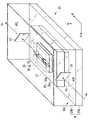
- FIG. 2 is a schematic perspective view for explaining the wavelength conversion device 30 of the first embodiment.
- the wavelength conversion device 30 includes a metal housing 28 and a multiplexer 14 that multiplexes the signal light 1a input to the wavelength conversion element 33 provided inside the metal housing 28 and the excitation light (not shown in the figure). and a demultiplexer 15 for demultiplexing the converted output signal light 3c wavelength-converted by the wavelength conversion element 33 and the excitation light (not shown).
- the signal light 1a is a fundamental wave with a wavelength of 1550 nm
- the converted output signal light 3c is a signal light with a wavelength of 775 nm, which is the second harmonic of the fundamental wave.
- the metal housing 28 has a bottom member 28A and a cover member 28B provided on the bottom member 28A.
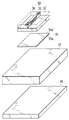
- the wavelength conversion element 33 including the optical waveguide core 31, the substrate 32 and the over-cladding layer 34, the temperature control element 26, the upper member 27, the substrate 32 and the upper member 27 of the wavelength conversion element 33. and a sheet-like resin layer provided between.
- a sheet-shaped resin layer is formed from an adhesive material, and the wavelength conversion element 33 and the upper member 27 are bonded by the sheet-shaped resin layer.
- the sheet-like adhesive layer is the adhesive sheet 35 .
- the temperature control element 26 of the first embodiment is, for example, a Peltier element, which generates heat on the surface facing the wavelength conversion element 33 and absorbs heat on the surface facing the bottom member 28A. The amount of heat generated and absorbed is controlled by the current supplied to the temperature control element 26 .
- the upper member 27 is located between the wavelength conversion element 33 and the temperature control element 26 and functions as a heat transfer member that transfers heat generated by the temperature control element 26 to the wavelength conversion element 33 .
- the material of the upper member 27 preferably contains one or more metals selected from stainless steel, copper-molybdenum steel, carbon steel, chromium-molybdenum steel, copper, phosphorus-deoxidized copper, oxygen-free copper, phosphor bronze, or brass. In the first embodiment, oxygen-free copper is used as the upper member 27 .
- the bottom member 28A and the cover member 28B are joined to seal the above configuration.
- the cover member 28B has an input port 400 for inputting the signal light 1a and an output port 401 for outputting the converted output signal light 3c.
- the upper and lower sides are defined according to the coordinate system shown in FIG. 2, and the side with the larger z coordinate is defined as "above” or "above” the side with the smaller z coordinate.
- An optical fiber connects between the optical waveguide core 31 and the input port 400 and between the output port 401 and the optical waveguide core 31, respectively.
- the branching filter 15 provided between the optical waveguide core 31 and the optical fiber on the output port 401 side reflects the pumping light (not shown) and transmits the converted output signal light 3c.
- the branching filter 15 on the output port 401 side transmits the excitation light, reflects the converted output signal light 3c, and the reflected light is optically transmitted to the optical fiber on the output port 401 side.
- the first embodiment uses a 45-degree mirror as the demultiplexer 15 .
- the demultiplexer 15 functions as a selective transmission/reflection section in the first embodiment.
- the bottom member 28A is preferably a member with high mechanical strength.
- the material of the bottom member 28A preferably contains one or more metals selected from tungsten, molybdenum, kovar, copper tungsten steel, stainless steel, or copper molybdenum steel.
- stainless steel is used as the bottom member 28A.
- a dry gas 302 is sealed inside the metal housing 28 to prevent dew condensation during temperature control.
- the inside of the metal housing 28 means the atmosphere around the wavelength conversion element 33, the temperature control element 26, the upper member 27, and the bottom member 28A sealed in the metal housing 28.
- FIG. Dry gas 302 preferably contains one or more selected from nitrogen, oxygen, argon, and helium. In the first embodiment, nitrogen gas is used as the dry gas 302 .
- the optical waveguide core 31 is an optical waveguide through which the signal light 1a is selectively transmitted without loss of intensity.
- the wavelength conversion element 33 having the optical waveguide core 31 is an optical waveguide type wavelength conversion element.
- the structure of the optical waveguide core 31 is not particularly limited as long as it has a function of outputting wavelength-converted converted output signal light 3c having a wavelength different from that of the signal light 1a when the wavelength of the signal light 1a is input.
- a structure in which the second-order nonlinear constant changes periodically along the traveling direction of light or with a period given a predetermined modulation to achieve quasi-phase matching for a single wavelength or multiple wavelengths, for example , multi-QPM (Quasi Phase Matching) elements can also be employed.
- the size of the optical waveguide core 31 is not particularly limited, and even if the core diameter is relatively large (10 ⁇ m) or larger, which allows light to propagate in multimode, light can propagate in single mode. It may have a small core diameter (10 ⁇ m) or less. Further, it may be an optical waveguide in which the core layer is thinned by the smart cut method or the like to try to reduce the core size, and the core diameter is very small (in units of nm). Also, the shape of the core is not particularly limited, and may be square, rectangular, trapezoidal, or any shape that can be processed.
- the substrate 32 is a ferroelectric substrate that is transparent to the signal light 1a, that is, does not absorb light.
- the substrate 32 functions as an undercladding layer for the optical waveguide core 31 when constructing the ridge-type optical waveguide, and receives the signal light 1a, excitation light (not shown), and wavelength conversion light rather than the optical waveguide core 31 . It is necessary that the converted output signal light 3c has a low refractive index.
- Ferroelectric materials employed for the substrate 32 include LiNbO 3 , KNbO 3 (potassium niobate), LiTaO 3 (lithium tantalate), LiNb(x)Ta( 1-x )O 3 (0 ⁇ x ⁇ 1) ( non-stoichiometric lithium tantalate), or KTiOPO 4 (potassium titanate phosphate), and at least one selected from Mg (magnesium), Zn (zinc), Sc (scandium), and In (indium) Those containing it as an additive are preferred.
- the overcladding layer 34 may be made of the same material as the substrate 32, which is the undercladding layer.
- the overcladding layer 34 may be air, chemical vapor deposition (CVD), flame hydrolysis deposition (FHD), glass deposited by sputtering, or the like.
- the over-cladding layer 34 is not particularly limited in terms of refractive index, and may be of any size as long as it has dimensions and shape for optical waveguide structural design.
- the overcladding layer 34 may be formed as required.
- the target is the wavelength conversion element 33 of the ridge-type optical waveguide in which the core layer that becomes the optical waveguide core 31 and the substrate 32 (undercladding layer) are directly bonded. That is, the wavelength conversion element 33 has a structure composed of an under clad layer, an over clad layer, and a core layer, and has an optical waveguide structure in which light propagates inside the core layer. Since the under-cladding layer and the core layer are directly bonded to each other, they have high resistance to optical damage, so that excitation light with a very high power density can be input into the optical waveguide.
- FIG. 3 is a schematic exploded perspective view of the wavelength conversion element 33, adhesive sheet 35, upper member 27 and temperature control element 26 shown in FIG.
- FIG. 4(a) is a schematic cross-sectional view of the wavelength conversion element 33, the adhesive sheet 35, the upper member 27 and the temperature control element 26 shown in FIG. 2 taken along the yz plane in the figure.
- FIG. 4(b) is a schematic cross-sectional view of the wavelength conversion element 33, the adhesive sheet 35, the upper member 27 and the temperature control element 26 shown in FIG. 2 taken along the xz plane.
- the adhesive sheet 35 of the first embodiment is provided on the entire surface between the wavelength conversion element 33 and the upper member 27.
- the adhesive sheet 35 is an adhesive sheet made of a material containing at least one of epoxy resin and polyimide resin. Such an adhesive sheet 35 also functions as an adhesive for bonding the substrate 32 of the wavelength conversion element 33 and the upper member 27 together.
- the surface 35 a of the adhesive sheet 35 facing the wavelength conversion element 33 adheres to the wavelength conversion element 33 and the surface 35 b facing the upper member 27 adheres to the upper member 27 .
- such a configuration is not limited to covering the entire surface of the adhesive sheet 35 , and may be a part of the adhesive sheet 35 .
- the lower surface of the substrate 32 of the wavelength conversion element 33 and the upper surface of the upper member 27 are connected via the adhesive sheet 35, and there are at least some portions that do not come into direct contact.
- the range in which the surface 35a of the adhesive sheet 35 adheres to the wavelength conversion element 33 and the surface 35b adheres to the upper member 27 is a range in which deformation of the upper member 27 is reduced. meets
- the adhesive sheet 35 of the first embodiment has elasticity necessary for alleviating the stress applied to the wavelength conversion element by the upper member 27, and can efficiently conduct heat from the temperature control element 26 to the substrate 32. Anything is fine.
- the adhesive sheet 35 may have any thickness as long as it fits inside the metal housing and does not interfere with other members. From the viewpoint of flatness and prevention of warping of the bonding structure, the thickness of the adhesive sheet 35 of the first embodiment is preferably 10 ⁇ m or more and 200 ⁇ m or less, for example.
- the adhesive sheet 35 of the first embodiment is not limited to one made of at least one of epoxy resin and polyimide resin as described above, and the elastic modulus, thermal conductivity and rigidity satisfy the required performance. Any material may be used if desired.
- a thermosetting resin is used for the adhesive sheet 35, but the present invention is not limited to this.
- a material that cures by any method may also be used. Such a curing method includes, for example, a photocuring method.
- the adhesive sheet 35 mainly includes curing agents, elastomers, fillers, curing accelerators, coupling agents, etc., in addition to epoxy resins or polyimide resins.
- Adhesive sheet 35 is produced by mixing such materials to form a layer of the adhesive composition on a support film, followed by heating and drying to bring it into a semi-cured state.
- the support film include films of polytetrafluoroethylene, polyethylene, polypropylene, polymethylpentene, polyethylene terephthalate, polyimide, and the like.
- the thickness of the support film may be, for example, about 10 ⁇ m to 200 ⁇ m.
- the adhesive composition may be applied to the support film by a known method to prepare the adhesive sheet 35.
- Examples of the application method include a knife coating method, a roll coating method, and a spray coating method. , a gravure coating method, a bar coating method, a curtain coating method, or the like may be used. Conditions for drying by heating are not particularly limited as long as the solvent used is sufficiently volatilized. After the surfaces 35a and 35b of the adhesive sheet 35 are attached to the substrate 32 and the upper member 27 of the wavelength conversion element 33, the adhesive sheet 35 is further heated to change from a semi-cured state to a fully cured state.
- the adhesive sheet 35 of the first embodiment is attached to the wavelength conversion element 33 and the upper member 27, and has excellent stress relaxation properties due to its smaller elastic modulus than solder or silver paste. Therefore, it is the most suitable adhesive for bonding dissimilar materials with different coefficients of thermal expansion.
- the adhesive sheet 35 is extremely flat due to the properties of the sheet or film, it is possible to realize an adhesive layer that is flatter than the applied liquid adhesive.
- the adhesive sheet 35 is made of a resin material, it has a relatively good elongation and can be easily embedded in the fine irregularities of the substrate 32 and the upper member 27 of the wavelength conversion element 33, thereby increasing the adhesive area. can. By such an action, the adhesion to the substrate 32 and the upper member 27 and the thermal conductivity can be enhanced.
- the adhesive sheet 35 can adhere the surfaces 35a and 35b to the substrate 32 or the upper member 27 and ensure the thickness between the surfaces 35a and 35b. For this reason, the adhesive sheet 35 has higher rigidity than a liquid adhesive made of a similar resin, and can reduce deformation of the upper member 27 and reduce warping of the joint structure with the wavelength conversion element 33 . can.
- the wavelength conversion device 30 of the first embodiment can relieve the stress applied to the wavelength conversion element during temperature control of the wavelength conversion element, and can realize stable operation and improved long-term reliability.
- the post-curing elastic modulus and thermal expansion coefficient of the adhesive sheet 35 can be adjusted.
- the elastic modulus of the adhesive sheet 35 is made smaller than the elastic modulus of a liquid adhesive made of a similar resin, the warping of the bonding structure between the substrate 32 and the upper member 27 can be further alleviated. can be done. Further, for example, it is preferable to adjust the amount of filler mixed so that the coefficient of thermal expansion of the adhesive sheet 35 approaches that of the substrate 32 and the upper member 27 .
- the sheet-like adhesive sheet 35 having a flat structure and having a smaller elastic modulus than known adhesive materials, the stress applied to the wavelength conversion element is relaxed and the temperature (control) applied to the wavelength conversion element 33 is reduced. temperature) is made uniform, and flat bonding between the wavelength conversion element 33 and the upper member 27 becomes possible. With such a configuration, it is possible to realize a wavelength conversion device with high optical characteristics and long-term reliability compared to known wavelength conversion devices.
- the manufacturing method of the wavelength conversion device of the first embodiment which will be described with reference to FIG. a step of processing the core substrate 311 to form an optical waveguide; a step of dividing the substrate 32 and the core substrate 311 into chips of the wavelength conversion element 33; 27 and a step of attaching the adhesive sheet 35 therebetween. Such steps will be sequentially described below.
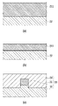
- (Substrate bonding process) 5(a), 5(b) and 5(c) are diagrams for explaining the manufacturing method of the wavelength conversion element 33 having a ridge type optical waveguide.
- a substrate 32 and a core substrate 311, which is a substrate serving as a core layer are directly bonded.
- the core substrate 311 is a substrate of nonlinear optical material.
- Direct bonding is a bonding technique that does not use an adhesive, and can improve resistance to light loss when high-intensity light is input. By selecting substrates 32 and core substrates 311 whose coefficients of thermal expansion are as close as possible in the bonding step, cracking of the substrate 32 can be suppressed in the subsequent heat treatment process.
- Direct bonding is a method in which the surfaces of the substrate 32 and the core substrate 311 are treated using chemicals, then the substrate 32 and the core substrate 311 are placed on top of each other, and the two are bonded using the attractive force between the surfaces.
- the surface treatment is performed by optimizing the conditions such as the temperature and the type of chemicals according to the types and combinations of the substrates 32 and core substrates 311 to be bonded.
- the bonding of the substrate 32 and the core substrate 311 must be performed in a clean atmosphere in which microparticles are minimized.
- direct bonding is performed at room temperature, but since the bonding strength at this time is small, it is necessary to perform heat treatment at a high temperature after that and perform diffusion bonding to improve the bonding strength.
- the bonded substrate 32 and core substrate 311 are free from microparticles and the like on the bonded surfaces, are void-free, and do not generate cracks or the like at room temperature.
- Direct bonding which allows substrates to be strongly bonded without using adhesives, etc., has features such as high optical damage resistance, long-term reliability, and ease of device design. This leads to stabilization of wave path characteristics.
- in light generation in the mid-infrared region using difference frequency generation, which is a type of nonlinear optical effect there is also the advantage of being able to avoid contamination by impurities and absorption by adhesives and the like.
- the core substrate 311 bonded to the substrate 32 is thinned as shown in FIG. 5(b).
- the method of thinning is not particularly limited, and thinning by grinding or polishing or thinning by smart cut may be used.
- thinning by grinding and polishing an apparatus in which the flatness of the surface plate for grinding and polishing is controlled is used to carry out grinding and polishing until an optical waveguide exists at an arbitrary depth.
- a mirror polished surface (optical end face) can be obtained by performing a polishing process after the grinding and polishing step.
- the parallelism of the substrate as a whole can be obtained by measuring the parallelism of the substrate (the difference between the maximum height and the minimum height of the substrate) using an optical parallelism measuring instrument.
- the thinning process using SmartCut mainly includes two processes: the ion implantation process and the thin film peeling process.
- the ion implantation process helium or hydrogen ions are implanted into a substrate that needs to be thinned with a second-order nonlinear optical effect. Ions are implanted from the surface of the core substrate 311 under a controlled acceleration voltage and a controlled dose, and trapped at a certain depth from the surface.
- the ions used are desirably smaller than the atoms forming the core substrate 311, such as hydrogen and helium.
- the substrate peeling step is a step of heat-treating the core substrate 311 implanted with ions and peeling the core substrate 311 along the damaged layer in the core substrate 311 .
- the heat treatment temperature in the substrate peeling step is performed at the Curie temperature of the secondary nonlinear optical crystal or less so as not to destroy the patterned polarization direction.
- the thinned core substrate 311 is then processed to form the optical waveguide core 31, as shown in FIG. 5(c).
- the formation method of the optical waveguide is not particularly limited, and a known method such as a dry etching process or cutting out the optical waveguide with a dicing saw may be used.
- the formation of the optical waveguide core 31 by dry etching is performed by etching the surface of the core substrate 311 using a dry etching apparatus.
- a resist pattern of an optical waveguide is formed on the surface of the core substrate 311 by a known photolithography process.
- An optical waveguide is formed by dry etching using the formed resist pattern as a mask.
- each of the divided substrate 32 and core substrate 311 is chipped so as to form the wavelength conversion element 33 of one chip. Dicing may be performed using a dicing saw, but the processing method is not particularly limited. Further, optical loss can be reduced when light enters or exits the chip by optically polishing the end face of the chip or coating it with an antireflection film after chipping. In the first embodiment, the optical characteristics of the chipped wavelength conversion element 33 are further evaluated.
- the wavelength conversion element 33 manufactured by the above steps is fixed to the upper surface of the upper member 27.
- an adhesive sheet 35 is inserted between the substrate 32 of the wavelength conversion element 33 and the upper surface of the upper member 27, and pressurized and heated to bond the substrate 32 and the upper member 27 together.
- Such bonding is a well-known bonding technique for conductive adhesives.
- the upper member 27, the bottom member 28A, and the temperature control element 26 between them are inserted and fixed inside the cover member 28B whose upper surface is open. Store later.
- the metal housing 28 is hermetically sealed by seam welding the upper surface of the cover member 28B of the metal housing 28 and the surrounding side surfaces in the atmosphere of the dry gas 302 .
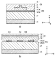
- FIG. 6(a) is a schematic cross-sectional view of the wavelength conversion element 33, the adhesive sheet 35, the upper member 27, and the temperature control element 26 of the second embodiment shown in FIG. is.
- FIG. 6(b) is a schematic cross-sectional view of the wavelength conversion element 33, the adhesive sheet 35, the upper member 27 and the temperature control element 26 shown in FIG. 2 taken along the xz plane.
- the second embodiment is different from the first embodiment in that a non-formation region 350, in which no adhesive sheet is formed, is formed between the substrate 32 and the upper member 27 instead of the adhesive sheet 35 of the first embodiment. It differs from the embodiment.
- the non-formation region corresponds to the resin layer non-formation region of the second embodiment.
- the second embodiment includes a plurality of adhesive sheets 351, 352, and 353 having a smaller area than the adhesive sheet 35 of the first embodiment, and bonds the substrate 32 and the upper member 27 together.
- non-formation regions 350 are formed on both sides of the adhesive sheets 351, 352, and 353 where no adhesive sheet is formed.
- the adhesive sheets 351, 352, and 353 all have the same length in the y direction as the adhesive sheet, but the length in the x direction is the same as that of the adhesive sheet 35. is shorter than
- Such adhesive sheets 351 , 352 , 353 are arranged in stripes on the upper surface of the upper member 27 .
- the surface 351a of the adhesive sheet 351 facing the substrate 32 adheres to the substrate 32
- the surface 351b facing the upper member 27 adheres to the upper member 27.
- FIG. Although illustration is omitted, the surfaces facing the substrate 32 and the surfaces facing the upper member 27 of the adhesive sheets 352 and 353 are also bonded to the opposing surfaces.
- the adhesive sheet can be processed into any size and shape by punching or laser processing. Therefore, the substrate 32 and the upper member 27 can be partially bonded together in addition to bonding the entire surface of the substrate 32 described in the first embodiment. With such a configuration, it is possible to selectively adjust the temperature of only a portion of the wavelength conversion element 33 .
- a temperature distribution exists inside the wavelength conversion element 33 during its operation. Specifically, the temperature near the light input port and the light output port of the optical waveguide core 31 is higher than the other portions.
- the second embodiment is effective in selectively adjusting the temperature of a part of the wavelength conversion element 33 and suppressing the temperature distribution in the optical waveguide.
- a higher effect can be obtained by introducing the dry gas 302 into the metal housing 28 and installing the wavelength conversion element 33 in the atmosphere.
Landscapes
- Physics & Mathematics (AREA)
- Nonlinear Science (AREA)
- General Physics & Mathematics (AREA)
- Optics & Photonics (AREA)
- Optical Modulation, Optical Deflection, Nonlinear Optics, Optical Demodulation, Optical Logic Elements (AREA)
Abstract
Description
図1(a)、図1(b)は、本実施形態の概要を説明するための図である。図1(a)は従来の波長変換装置における高温動作時の反りを示す模式図、図1(b)は本実施形態の波長変換装置の反りを解消するための構造を示す模式図である。図1(a)、図1(b)のいずれにあっても、波長変換装置は、例えばペルチェ素子等の温度制御素子と波長変換素子200とを熱伝導のために設けられた上部部材100を介して接合している。図1(a)の従来の波長変換装置は、波長変換素子200と上部部材100とが導電性接着剤で接着されている。図1(b)の波長変換装置は、波長変換素子200と上部部材100とを導電性接着剤で接着することに代えて、シートあるいはフィルム状の樹脂層を含む接着シート300により接合している。接着シート300は、半田や銀ペーストと比較して弾性率が小さく、また、樹脂を材料とする導電性接着剤よりも平坦であって、かつ、上部部材100の変形を緩和することに充分な剛性を得る厚さを有している。なお、ここで、シートとフィルムとは、いずれも厚さが比較的薄く、かつ均一な部材を指し、その厚さや平坦性を規定するものではない。
(波長変換装置)
図2は、第1の実施形態の波長変換装置30を説明するための模式的な斜視図である。波長変換装置30は、金属筐体28と、金属筐体28の内部に設けられた波長変換素子33に入力される信号光1aと励起光(図中省略)とを合波する合波器14と、波長変換素子33により波長変換された変換出力信号光3cと励起光(図中省略)とを分波する分波器15と、を備えている。信号光1aは、波長1550nmの基本波であり、変換出力信号光3cは、基本波の第二高調波である波長775nmの信号光である。
次に、以上説明した波長変換装置の製造方法を説明する。図5を参照して説明する第1の実施形態の波長変換装置の製造方法は、アンダークラッド層となる基板32と、光導波路コア31となるコア基板311とを接合する工程と、コア基板311を薄膜化する工程と、コア基板311を加工して光導波路を形成する工程と、基板32及びコア基板311を分割して波長変換素子33をチップ化する工程と、波長変換素子33を上部部材27に接着シート35を挟んで取り付ける工程と、を含んでいる。以下、このような工程を順次説明する。
図5(a)、図5(b)及び図5(c)は、リッジ型の光導波路を有する波長変換素子33の製造方法を説明するための図である。第1の実施形態は、図5(a)に示すように、基板32と、コア層となる基板であるコア基板311と、を直接接合により接合する。コア基板311は、非線形光学材料の基板である。直接接合は、接着剤を用いない接合技術であり、高強度の光を入力した場合の光損失耐性を向上させることができる。接合工程において、基板32とコア基板311とに熱膨張係数が可能な限り近いものを選定することにより、後の熱処理プロセスにおいて基板32の割れを抑制することが可能になる。
基板32と貼り合わされたコア基板311は、図5(b)に示すように、薄膜化される。第1の実施形態の薄膜化工程は、薄膜化の手法に特に制限はなく、研削、研磨による薄膜化でもスマートカットによる薄膜化のいずれであってもよい。研削、研磨による薄膜化では、研削研磨用の定盤の平坦度が管理された装置を用いて、任意の深さに光導波路が存在するようになるまで研削研磨加工を施す。研削研磨工程終了後にポリッシング加工を行うことで、鏡面の研磨表面(光学端面)を得ることができる。最終的に基板の平行度(基板の最大高さと最小高さの差)を光学的な平行度測定器を用いて測定することで、基板全体としての平行度を得ることができる。
第1の実施形態は、次に、図5(c)に示すように、薄膜化されたコア基板311を加工して光導波路コア31を形成する。光導波路の形成は、形成方法に特に制限はなく、ドライエッチングプロセスやダイシングソーによる光導波路の切り出し等の公知の方法を用いてもよい。ドライエッチングによる光導波路コア31の形成は、ドライエッチング装置を用いてコア基板311の表面をエッチングすることにより行われる。この際、コア基板311の表面には公知のフォトリソグラフィのプロセスによって光導波路のレジストパターンが形成される。形成されたレジストパターンをマスクとし、ドライエッチングすることによって光導波路が形成される。
次に、第2の実施形態を説明する。第2の実施形態の波長変換装置の斜視図は、第1の実施形態で説明した図2に示す構成と同様であるため、図示及び説明を省く。図6(a)は、図2に示す第2の実施形態の波長変換素子33、接着シート35、上部部材27及び温度制御素子26を図中のy-z平面で切断した模式的な断面図である。図6(b)は、図2に示す波長変換素子33、接着シート35、上部部材27及び温度制御素子26をx-z平面で切断した模式的な断面図である。第2の実施形態は、第1の実施形態の接着シート35に代えて、基板32と上部部材27との間において、接着シートが形成されない、非形成領域350が形成される点で第1の実施形態と相違する。非形成領域は、第2の実施形態の樹脂層非形成領域に相当する。
3c 変換出力信号光
14 合波器
15 分波器
26,260 温度制御素子
27,100,270 上部部材
28,290 金属筐体
28A,280 底面部材
28B カバー部材
30,200 波長変換装置
31,310 光導波路コア
32,320 基板
33,330 波長変換素子
34,340 オーバークラッド層
35,300,351,352,353 接着シート
35a,35b,351a,351b 面
311 コア基板
400 入力ポート
401 出力ポート
350 非形成領域
Claims (8)
- 波長変換装置であって、
励起光及び信号光を入力し、波長変換された変換出力信号光を出力する波長変換素子と、
前記波長変換素子の温度を制御する温度制御部と、
前記波長変換素子と前記温度制御部との間に設けられ、前記温度制御部と前記波長変換素子との間で熱を伝達する熱伝達部材と、
前記波長変換素子と前記熱伝達部材との間に設けられるシート状の樹脂層と、を備え、
前記シート状の樹脂層の少なくとも一部は、前記波長変換素子に向かう面が前記波長変換素子と接着し、前記熱伝達部材に向かう面が前記熱伝達部材と接着する、波長変換装置。 - 前記シート状の樹脂層における前記波長変換素子から前記熱伝達部材に向かう長さは、10μm以上、200μm以下である、請求項1に記載の波長変換装置。
- 前記波長変換素子と前記熱伝達部材との間において、前記シート状の樹脂層が形成されない、樹脂層非形成領域が形成される、請求項1または2に記載の波長変換装置。
- 前記シート状の樹脂層は、エポキシ系樹脂、ポリイミド系樹脂の少なくとも一方を材料に含む、請求項1から3のいずれか一項に記載の波長変換装置。
- 前記波長変換素子は、LiNbO3、LiTaO3もしくはLiNb(x)Ta(1-x)O3(0≦x≦1)のいずれか、または、これらにMg、Zn、Sc、Inからなる群から選ばれた少なくとも一種を添加物として含有したものである、請求項1から4のいずれか一項に記載の波長変換装置。
- 前記波長変換素子は、光導波路を備える光導波路型波長変換素子であり、かつ、分極が周期的に反転されている、請求項1から5のいずれか一項に記載の波長変換装置。
- 前記変換出力信号光を導出する光ファイバと、
前記波長変換素子と光ファイバとの間に設けられ、前記励起光及び前記変換出力信号光のうちの一方を透過すると共に他方を反射する選択的透過反射部と、をさらに備え、
前記選択的透過反射部は、透過または反射した前記変換出力信号光を前記光ファイバと光学的に接続する、請求項1から6のいずれか一項に記載の波長変換装置。 - 波長変換素子を有する波長変換装置の製造方法であって、
前記波長変換素子の温度を制御する温度制御部の熱を前記波長変換素子に伝達する熱伝達部材と前記波長変換素子との間にシート状の樹脂層を挿入する工程と、
前記シート状の樹脂層を加圧すると共に硬化させ、前記波長変換素子と前記熱伝達部材とを接着する工程と、
接着された前記波長変換素子及び前記熱伝達部材を一部が開口している筐体の内部に収容し、前記筐体の底面部材と前記熱伝達部材との間に前記温度制御部を挿入する工程と、
前記筐体の開口部分を封止する工程と、を含む、波長変換装置の製造方法。
Priority Applications (3)
| Application Number | Priority Date | Filing Date | Title |
|---|---|---|---|
| PCT/JP2021/019581 WO2022249234A1 (ja) | 2021-05-24 | 2021-05-24 | 波長変換装置及び波長変換装置の製造方法 |
| US18/554,590 US20240184147A1 (en) | 2021-05-24 | 2021-05-24 | Wavelength Conversion Device And Manufacturing Method Of Wavelength Conversion Device |
| JP2023523718A JP7553868B2 (ja) | 2021-05-24 | 2021-05-24 | 波長変換装置及び波長変換装置の製造方法 |
Applications Claiming Priority (1)
| Application Number | Priority Date | Filing Date | Title |
|---|---|---|---|
| PCT/JP2021/019581 WO2022249234A1 (ja) | 2021-05-24 | 2021-05-24 | 波長変換装置及び波長変換装置の製造方法 |
Publications (1)
| Publication Number | Publication Date |
|---|---|
| WO2022249234A1 true WO2022249234A1 (ja) | 2022-12-01 |
Family
ID=84229641
Family Applications (1)
| Application Number | Title | Priority Date | Filing Date |
|---|---|---|---|
| PCT/JP2021/019581 Ceased WO2022249234A1 (ja) | 2021-05-24 | 2021-05-24 | 波長変換装置及び波長変換装置の製造方法 |
Country Status (3)
| Country | Link |
|---|---|
| US (1) | US20240184147A1 (ja) |
| JP (1) | JP7553868B2 (ja) |
| WO (1) | WO2022249234A1 (ja) |
Cited By (1)
| Publication number | Priority date | Publication date | Assignee | Title |
|---|---|---|---|---|
| WO2026009282A1 (ja) * | 2024-07-01 | 2026-01-08 | Ntt株式会社 | 波長変換装置 |
Citations (7)
| Publication number | Priority date | Publication date | Assignee | Title |
|---|---|---|---|---|
| WO2004049526A1 (ja) * | 2002-11-12 | 2004-06-10 | Matsushita Electric Industrial Co., Ltd. | レーザモジュールおよびその作製方法 |
| JP2009003210A (ja) * | 2007-06-22 | 2009-01-08 | Panasonic Corp | 二次高調波発生装置 |
| JP2009194371A (ja) * | 2008-01-16 | 2009-08-27 | Panasonic Corp | 波長変換レーザ光源、これを備えた2次元画像表示装置およびレーザ光源装置 |
| US20100073761A1 (en) * | 2008-09-19 | 2010-03-25 | Korea Electronics Technology Institute | Wavelength conversion device package |
| JP2010109132A (ja) * | 2008-10-30 | 2010-05-13 | Yamaha Corp | 熱電モジュールを備えたパッケージおよびその製造方法 |
| JP2012053488A (ja) * | 2004-10-12 | 2012-03-15 | Ngk Insulators Ltd | 光導波路基板および高調波発生デバイス |
| US9397469B1 (en) * | 2015-04-06 | 2016-07-19 | Voxtel, Inc. | Er,Yb:YAB laser system |
Family Cites Families (8)
| Publication number | Priority date | Publication date | Assignee | Title |
|---|---|---|---|---|
| JP3966958B2 (ja) * | 1997-09-26 | 2007-08-29 | 富士フイルム株式会社 | 固体レーザー |
| JP3968610B2 (ja) * | 1998-05-27 | 2007-08-29 | Smc株式会社 | 半導体処理液用冷却加熱装置 |
| JP3641232B2 (ja) * | 2001-11-13 | 2005-04-20 | 本田技研工業株式会社 | インバータ装置及びその製造方法 |
| JP4843506B2 (ja) * | 2005-01-17 | 2011-12-21 | 日本電信電話株式会社 | 変調機能付光源装置とその駆動方法 |
| JP4277908B2 (ja) * | 2007-02-06 | 2009-06-10 | セイコーエプソン株式会社 | 光源装置、照明装置、モニタ装置及びプロジェクタ |
| JP5177229B2 (ja) * | 2009-05-21 | 2013-04-03 | トヨタ自動車株式会社 | 高熱伝導絶縁樹脂の接着方法 |
| JP5407881B2 (ja) * | 2010-01-13 | 2014-02-05 | トヨタ自動車株式会社 | パワーモジュール製造方法およびその方法により製造したパワーモジュール |
| CN102782836B (zh) * | 2010-02-24 | 2016-03-09 | 丰田自动车株式会社 | 半导体模块的制造方法、半导体模块以及制造装置 |
-
2021
- 2021-05-24 WO PCT/JP2021/019581 patent/WO2022249234A1/ja not_active Ceased
- 2021-05-24 JP JP2023523718A patent/JP7553868B2/ja active Active
- 2021-05-24 US US18/554,590 patent/US20240184147A1/en active Pending
Patent Citations (7)
| Publication number | Priority date | Publication date | Assignee | Title |
|---|---|---|---|---|
| WO2004049526A1 (ja) * | 2002-11-12 | 2004-06-10 | Matsushita Electric Industrial Co., Ltd. | レーザモジュールおよびその作製方法 |
| JP2012053488A (ja) * | 2004-10-12 | 2012-03-15 | Ngk Insulators Ltd | 光導波路基板および高調波発生デバイス |
| JP2009003210A (ja) * | 2007-06-22 | 2009-01-08 | Panasonic Corp | 二次高調波発生装置 |
| JP2009194371A (ja) * | 2008-01-16 | 2009-08-27 | Panasonic Corp | 波長変換レーザ光源、これを備えた2次元画像表示装置およびレーザ光源装置 |
| US20100073761A1 (en) * | 2008-09-19 | 2010-03-25 | Korea Electronics Technology Institute | Wavelength conversion device package |
| JP2010109132A (ja) * | 2008-10-30 | 2010-05-13 | Yamaha Corp | 熱電モジュールを備えたパッケージおよびその製造方法 |
| US9397469B1 (en) * | 2015-04-06 | 2016-07-19 | Voxtel, Inc. | Er,Yb:YAB laser system |
Cited By (1)
| Publication number | Priority date | Publication date | Assignee | Title |
|---|---|---|---|---|
| WO2026009282A1 (ja) * | 2024-07-01 | 2026-01-08 | Ntt株式会社 | 波長変換装置 |
Also Published As
| Publication number | Publication date |
|---|---|
| JP7553868B2 (ja) | 2024-09-19 |
| JPWO2022249234A1 (ja) | 2022-12-01 |
| US20240184147A1 (en) | 2024-06-06 |
Similar Documents
| Publication | Publication Date | Title |
|---|---|---|
| CN112969960B (zh) | 波长转换装置 | |
| JP5083865B2 (ja) | 光導波路基板および高調波発生デバイス | |
| WO2005019913A1 (ja) | 光導波路デバイスおよび進行波形光変調器 | |
| JP2008250258A (ja) | 光制御素子 | |
| JP2003140214A (ja) | 波長変換素子用薄膜基板の製造方法及び波長変換素子の製造方法 | |
| JP4907574B2 (ja) | 光変調器 | |
| US20110032600A1 (en) | Electromagnetic wave oscillating devices | |
| JP7295467B2 (ja) | 光学素子及びその製造方法 | |
| JP7473850B2 (ja) | 波長変換装置 | |
| JP7062937B2 (ja) | 光学素子およびその製造方法 | |
| JP7319582B2 (ja) | 波長変換装置 | |
| JP3506304B2 (ja) | 光発生装置及びその製造方法 | |
| JP2003270467A (ja) | 光導波路デバイスの製造方法、光導波路デバイス並びに当該光導波路デバイスを用いたコヒーレント光源及び光学装置 | |
| JP7553868B2 (ja) | 波長変換装置及び波長変換装置の製造方法 | |
| CN100439953C (zh) | 光波导路装置和使用它的相干光源及光学装置 | |
| CN113612108B (zh) | 一种基于斜切非线性晶体脊型波导的频率转换器及其制备方法 | |
| JP6774372B2 (ja) | 光学素子 | |
| Feng et al. | A bond-free PPLN thin film ridge waveguide | |
| JP4803546B2 (ja) | 波長変換導波路素子及びその製造方法 | |
| JP2014211539A (ja) | 波長変換素子 | |
| JP4682111B2 (ja) | 導波路型光デバイス及びその製造方法 | |
| WO2023218646A1 (ja) | 波長変換システム | |
| US20240152025A1 (en) | Optical Wavelength Conversion Device | |
| CN115698793A (zh) | 光波导元件及使用了该光波导元件的光调制器件以及光发送装置 | |
| JP7861632B2 (ja) | 光導波路素子及びそれを用いた光変調デバイス並びに光送信装置 |
Legal Events
| Date | Code | Title | Description |
|---|---|---|---|
| 121 | Ep: the epo has been informed by wipo that ep was designated in this application |
Ref document number: 21942892 Country of ref document: EP Kind code of ref document: A1 |
|
| WWE | Wipo information: entry into national phase |
Ref document number: 2023523718 Country of ref document: JP |
|
| WWE | Wipo information: entry into national phase |
Ref document number: 18554590 Country of ref document: US |
|
| NENP | Non-entry into the national phase |
Ref country code: DE |
|
| 122 | Ep: pct application non-entry in european phase |
Ref document number: 21942892 Country of ref document: EP Kind code of ref document: A1 |