WO2022244384A1 - 光検出装置および測距装置 - Google Patents
光検出装置および測距装置 Download PDFInfo
- Publication number
- WO2022244384A1 WO2022244384A1 PCT/JP2022/009234 JP2022009234W WO2022244384A1 WO 2022244384 A1 WO2022244384 A1 WO 2022244384A1 JP 2022009234 W JP2022009234 W JP 2022009234W WO 2022244384 A1 WO2022244384 A1 WO 2022244384A1
- Authority
- WO
- WIPO (PCT)
- Prior art keywords
- substrate
- photodetector
- light
- conductivity type
- section
- Prior art date
- Legal status (The legal status is an assumption and is not a legal conclusion. Google has not performed a legal analysis and makes no representation as to the accuracy of the status listed.)
- Ceased
Links
Images









Classifications
-
- G—PHYSICS
- G01—MEASURING; TESTING
- G01S—RADIO DIRECTION-FINDING; RADIO NAVIGATION; DETERMINING DISTANCE OR VELOCITY BY USE OF RADIO WAVES; LOCATING OR PRESENCE-DETECTING BY USE OF THE REFLECTION OR RERADIATION OF RADIO WAVES; ANALOGOUS ARRANGEMENTS USING OTHER WAVES
- G01S7/00—Details of systems according to groups G01S13/00, G01S15/00, G01S17/00
- G01S7/48—Details of systems according to groups G01S13/00, G01S15/00, G01S17/00 of systems according to group G01S17/00
- G01S7/483—Details of pulse systems
- G01S7/486—Receivers
- G01S7/4865—Time delay measurement, e.g. time-of-flight measurement, time of arrival measurement or determining the exact position of a peak
-
- G—PHYSICS
- G01—MEASURING; TESTING
- G01J—MEASUREMENT OF INTENSITY, VELOCITY, SPECTRAL CONTENT, POLARISATION, PHASE OR PULSE CHARACTERISTICS OF INFRARED, VISIBLE OR ULTRAVIOLET LIGHT; COLORIMETRY; RADIATION PYROMETRY
- G01J1/00—Photometry, e.g. photographic exposure meter
- G01J1/02—Details
-
- G—PHYSICS
- G01—MEASURING; TESTING
- G01J—MEASUREMENT OF INTENSITY, VELOCITY, SPECTRAL CONTENT, POLARISATION, PHASE OR PULSE CHARACTERISTICS OF INFRARED, VISIBLE OR ULTRAVIOLET LIGHT; COLORIMETRY; RADIATION PYROMETRY
- G01J1/00—Photometry, e.g. photographic exposure meter
- G01J1/42—Photometry, e.g. photographic exposure meter using electric radiation detectors
-
- G—PHYSICS
- G01—MEASURING; TESTING
- G01S—RADIO DIRECTION-FINDING; RADIO NAVIGATION; DETERMINING DISTANCE OR VELOCITY BY USE OF RADIO WAVES; LOCATING OR PRESENCE-DETECTING BY USE OF THE REFLECTION OR RERADIATION OF RADIO WAVES; ANALOGOUS ARRANGEMENTS USING OTHER WAVES
- G01S17/00—Systems using the reflection or reradiation of electromagnetic waves other than radio waves, e.g. lidar systems
- G01S17/02—Systems using the reflection of electromagnetic waves other than radio waves
- G01S17/06—Systems determining position data of a target
- G01S17/08—Systems determining position data of a target for measuring distance only
- G01S17/10—Systems determining position data of a target for measuring distance only using transmission of interrupted, pulse-modulated waves
-
- G—PHYSICS
- G01—MEASURING; TESTING
- G01S—RADIO DIRECTION-FINDING; RADIO NAVIGATION; DETERMINING DISTANCE OR VELOCITY BY USE OF RADIO WAVES; LOCATING OR PRESENCE-DETECTING BY USE OF THE REFLECTION OR RERADIATION OF RADIO WAVES; ANALOGOUS ARRANGEMENTS USING OTHER WAVES
- G01S17/00—Systems using the reflection or reradiation of electromagnetic waves other than radio waves, e.g. lidar systems
- G01S17/88—Lidar systems specially adapted for specific applications
- G01S17/89—Lidar systems specially adapted for specific applications for mapping or imaging
- G01S17/894—Three-dimensional [3D] imaging with simultaneous measurement of time-of-flight at a two-dimensional [2D] array of receiver pixels, e.g. time-of-flight cameras or flash lidar
-
- G—PHYSICS
- G01—MEASURING; TESTING
- G01S—RADIO DIRECTION-FINDING; RADIO NAVIGATION; DETERMINING DISTANCE OR VELOCITY BY USE OF RADIO WAVES; LOCATING OR PRESENCE-DETECTING BY USE OF THE REFLECTION OR RERADIATION OF RADIO WAVES; ANALOGOUS ARRANGEMENTS USING OTHER WAVES
- G01S17/00—Systems using the reflection or reradiation of electromagnetic waves other than radio waves, e.g. lidar systems
- G01S17/88—Lidar systems specially adapted for specific applications
- G01S17/93—Lidar systems specially adapted for specific applications for anti-collision purposes
- G01S17/931—Lidar systems specially adapted for specific applications for anti-collision purposes of land vehicles
-
- G—PHYSICS
- G01—MEASURING; TESTING
- G01S—RADIO DIRECTION-FINDING; RADIO NAVIGATION; DETERMINING DISTANCE OR VELOCITY BY USE OF RADIO WAVES; LOCATING OR PRESENCE-DETECTING BY USE OF THE REFLECTION OR RERADIATION OF RADIO WAVES; ANALOGOUS ARRANGEMENTS USING OTHER WAVES
- G01S7/00—Details of systems according to groups G01S13/00, G01S15/00, G01S17/00
- G01S7/48—Details of systems according to groups G01S13/00, G01S15/00, G01S17/00 of systems according to group G01S17/00
- G01S7/481—Constructional features, e.g. arrangements of optical elements
-
- G—PHYSICS
- G01—MEASURING; TESTING
- G01S—RADIO DIRECTION-FINDING; RADIO NAVIGATION; DETERMINING DISTANCE OR VELOCITY BY USE OF RADIO WAVES; LOCATING OR PRESENCE-DETECTING BY USE OF THE REFLECTION OR RERADIATION OF RADIO WAVES; ANALOGOUS ARRANGEMENTS USING OTHER WAVES
- G01S7/00—Details of systems according to groups G01S13/00, G01S15/00, G01S17/00
- G01S7/48—Details of systems according to groups G01S13/00, G01S15/00, G01S17/00 of systems according to group G01S17/00
- G01S7/481—Constructional features, e.g. arrangements of optical elements
- G01S7/4816—Constructional features, e.g. arrangements of optical elements of receivers alone
-
- H—ELECTRICITY
- H10—SEMICONDUCTOR DEVICES; ELECTRIC SOLID-STATE DEVICES NOT OTHERWISE PROVIDED FOR
- H10F—INORGANIC SEMICONDUCTOR DEVICES SENSITIVE TO INFRARED RADIATION, LIGHT, ELECTROMAGNETIC RADIATION OF SHORTER WAVELENGTH OR CORPUSCULAR RADIATION
- H10F30/00—Individual radiation-sensitive semiconductor devices in which radiation controls the flow of current through the devices, e.g. photodetectors
- H10F30/20—Individual radiation-sensitive semiconductor devices in which radiation controls the flow of current through the devices, e.g. photodetectors the devices having potential barriers, e.g. phototransistors
- H10F30/21—Individual radiation-sensitive semiconductor devices in which radiation controls the flow of current through the devices, e.g. photodetectors the devices having potential barriers, e.g. phototransistors the devices being sensitive to infrared, visible or ultraviolet radiation
- H10F30/22—Individual radiation-sensitive semiconductor devices in which radiation controls the flow of current through the devices, e.g. photodetectors the devices having potential barriers, e.g. phototransistors the devices being sensitive to infrared, visible or ultraviolet radiation the devices having only one potential barrier, e.g. photodiodes
- H10F30/225—Individual radiation-sensitive semiconductor devices in which radiation controls the flow of current through the devices, e.g. photodetectors the devices having potential barriers, e.g. phototransistors the devices being sensitive to infrared, visible or ultraviolet radiation the devices having only one potential barrier, e.g. photodiodes the potential barrier working in avalanche mode, e.g. avalanche photodiodes
-
- H—ELECTRICITY
- H10—SEMICONDUCTOR DEVICES; ELECTRIC SOLID-STATE DEVICES NOT OTHERWISE PROVIDED FOR
- H10F—INORGANIC SEMICONDUCTOR DEVICES SENSITIVE TO INFRARED RADIATION, LIGHT, ELECTROMAGNETIC RADIATION OF SHORTER WAVELENGTH OR CORPUSCULAR RADIATION
- H10F39/00—Integrated devices, or assemblies of multiple devices, comprising at least one element covered by group H10F30/00, e.g. radiation detectors comprising photodiode arrays
- H10F39/10—Integrated devices
- H10F39/12—Image sensors
-
- H—ELECTRICITY
- H10—SEMICONDUCTOR DEVICES; ELECTRIC SOLID-STATE DEVICES NOT OTHERWISE PROVIDED FOR
- H10F—INORGANIC SEMICONDUCTOR DEVICES SENSITIVE TO INFRARED RADIATION, LIGHT, ELECTROMAGNETIC RADIATION OF SHORTER WAVELENGTH OR CORPUSCULAR RADIATION
- H10F39/00—Integrated devices, or assemblies of multiple devices, comprising at least one element covered by group H10F30/00, e.g. radiation detectors comprising photodiode arrays
- H10F39/10—Integrated devices
- H10F39/12—Image sensors
- H10F39/18—Complementary metal-oxide-semiconductor [CMOS] image sensors; Photodiode array image sensors
- H10F39/184—Infrared image sensors
-
- H—ELECTRICITY
- H10—SEMICONDUCTOR DEVICES; ELECTRIC SOLID-STATE DEVICES NOT OTHERWISE PROVIDED FOR
- H10F—INORGANIC SEMICONDUCTOR DEVICES SENSITIVE TO INFRARED RADIATION, LIGHT, ELECTROMAGNETIC RADIATION OF SHORTER WAVELENGTH OR CORPUSCULAR RADIATION
- H10F39/00—Integrated devices, or assemblies of multiple devices, comprising at least one element covered by group H10F30/00, e.g. radiation detectors comprising photodiode arrays
- H10F39/80—Constructional details of image sensors
- H10F39/806—Optical elements or arrangements associated with the image sensors
- H10F39/8063—Microlenses
-
- H—ELECTRICITY
- H10—SEMICONDUCTOR DEVICES; ELECTRIC SOLID-STATE DEVICES NOT OTHERWISE PROVIDED FOR
- H10F—INORGANIC SEMICONDUCTOR DEVICES SENSITIVE TO INFRARED RADIATION, LIGHT, ELECTROMAGNETIC RADIATION OF SHORTER WAVELENGTH OR CORPUSCULAR RADIATION
- H10F39/00—Integrated devices, or assemblies of multiple devices, comprising at least one element covered by group H10F30/00, e.g. radiation detectors comprising photodiode arrays
- H10F39/80—Constructional details of image sensors
- H10F39/807—Pixel isolation structures
-
- H—ELECTRICITY
- H10—SEMICONDUCTOR DEVICES; ELECTRIC SOLID-STATE DEVICES NOT OTHERWISE PROVIDED FOR
- H10F—INORGANIC SEMICONDUCTOR DEVICES SENSITIVE TO INFRARED RADIATION, LIGHT, ELECTROMAGNETIC RADIATION OF SHORTER WAVELENGTH OR CORPUSCULAR RADIATION
- H10F39/00—Integrated devices, or assemblies of multiple devices, comprising at least one element covered by group H10F30/00, e.g. radiation detectors comprising photodiode arrays
- H10F39/80—Constructional details of image sensors
- H10F39/809—Constructional details of image sensors of hybrid image sensors
-
- H—ELECTRICITY
- H10—SEMICONDUCTOR DEVICES; ELECTRIC SOLID-STATE DEVICES NOT OTHERWISE PROVIDED FOR
- H10W—GENERIC PACKAGES, INTERCONNECTIONS, CONNECTORS OR OTHER CONSTRUCTIONAL DETAILS OF DEVICES COVERED BY CLASS H10
- H10W72/00—Interconnections or connectors in packages
- H10W72/90—Bond pads, in general
-
- H—ELECTRICITY
- H10—SEMICONDUCTOR DEVICES; ELECTRIC SOLID-STATE DEVICES NOT OTHERWISE PROVIDED FOR
- H10W—GENERIC PACKAGES, INTERCONNECTIONS, CONNECTORS OR OTHER CONSTRUCTIONAL DETAILS OF DEVICES COVERED BY CLASS H10
- H10W90/00—Package configurations
- H10W90/701—Package configurations characterised by the relative positions of pads or connectors relative to package parts
- H10W90/791—Package configurations characterised by the relative positions of pads or connectors relative to package parts of direct-bonded pads
- H10W90/792—Package configurations characterised by the relative positions of pads or connectors relative to package parts of direct-bonded pads between multiple chips
Definitions
- the present disclosure relates to, for example, a photodetector using an avalanche photodiode and a rangefinder including the same.
- Patent Document 1 a first photoelectric conversion element made of silicon and a second photoelectric conversion element made of a semiconductor material having a bandgap smaller than that of silicon are provided on the main surface of a silicon semiconductor substrate. is disclosed.
- a photodetector has a first surface that serves as a light receiving surface and a second surface that faces the first surface.
- a first substrate having a light-receiving portion that generates an amount of charge by photoelectric conversion; a third surface disposed on the second surface side of the first substrate and facing the second surface; a second substrate having a fourth surface facing the second substrate, having a bandgap wider than that of the first substrate, and having a multiplication section for each pixel for avalanche-multiplying the charge generated in the light-receiving section; a first electrode provided on the first surface of the first substrate and electrically connected to the light receiving section; and a first electrode provided on the fourth surface of the second substrate and electrically connected to the multiplier section. and a second electrode.
- a distance measuring device includes an optical system, a photodetector, and a signal processing circuit that calculates a distance to an object to be measured from an output signal of the photodetector. As a device, it has the photodetector of one embodiment of the present disclosure.
- the light receiving section is provided on the first substrate with a narrow bandgap
- the multiplication section is provided on the second substrate with a wider bandgap than the first substrate. I tried to set it on the board of As a result, generation of dark current in the multiplication section is reduced while improving the quantum efficiency for near infrared (NIR) and short infrared (SWIR) wavelengths.
- NIR near infrared
- SWIR short infrared
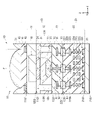
- FIG. 1 is a cross-sectional schematic diagram showing an example of a configuration of a photodetector according to an embodiment of the present disclosure
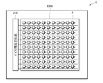
- FIG. 2 is a block diagram showing an example of an overall schematic configuration of the photodetector shown in FIG. 1;
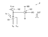
- FIG. 2 is an example of an equivalent circuit diagram of a unit pixel of the photodetector shown in FIG. 1.
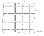
- FIG. 2 is a schematic plan view for explaining the layout of the anode of the photodetector shown in FIG. 1.
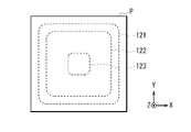
- FIG. FIG. 2 is a schematic plan view for explaining the configuration of a multiplication section in a unit pixel of the photodetector shown in FIG.
- FIG. 1; 2 is a schematic cross-sectional view for explaining an example of routing of an anode electrode of the photodetector shown in FIG. 1.
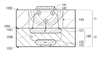
- FIG. 2 is a schematic diagram for explaining the flow of charges in the photodetector shown in FIG. 1;
- FIG. FIG. 5 is a schematic diagram for explaining the flow of charges in a photodetector as a comparative example;
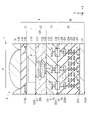
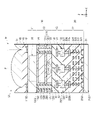
- FIG. 4 is a schematic cross-sectional view showing another example of the configuration of the photodetector according to the embodiment of the present disclosure;
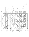
- FIG. 4 is a schematic cross-sectional view showing an example of a configuration of a photodetector according to Modification 1 of the present disclosure;
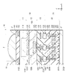
- FIG. 5 is a schematic cross-sectional view showing an example of the configuration of a photodetector according to Modification 2 of the present disclosure
- FIG. 11 is a schematic cross-sectional view showing an example of a configuration of a photodetector according to Modification 3 of the present disclosure
- FIG. 11 is a schematic cross-sectional view showing an example of a configuration of a photodetector according to Modification 4 of the present disclosure
- FIG. 12 is a schematic cross-sectional view showing another example of the configuration of the photodetector according to Modification 4 of the present disclosure
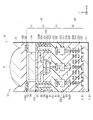
- FIG. 11 is a schematic cross-sectional view showing an example of a configuration of a photodetector according to Modification 5 of the present disclosure
- FIG. 12 is a schematic cross-sectional view showing another example of the configuration of the photodetector according to Modification 5 of the present disclosure
- FIG. 12 is a schematic cross-sectional view showing another example of the configuration of the photodetector according to Modification 5 of the present disclosure
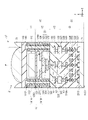
- FIG. 11 is a cross-sectional schematic diagram illustrating an example of a configuration of a photodetector according to Modification 6 of the present disclosure
- FIG. 12 is a schematic cross-sectional view showing another example of the configuration of the photodetector according to Modification 6 of the present disclosure
- FIG. 12 is a schematic cross-sectional view showing another example of the configuration of the photodetector according to Modification 6 of the present disclosure
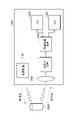
- 2 is a functional block diagram showing an example of an electronic device using the photodetector shown in FIG. 1 and the like
- FIG. 1 is a block diagram showing an example of a schematic configuration of a vehicle control system
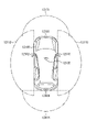
- FIG. 4 is an explanatory diagram showing an example of installation positions of an outside information detection unit and an imaging unit;
- Embodiment photodetection device in which a light receiving section is provided on a Ge substrate, a multiplication section is provided on a Si substrate, and an anode is provided on the light receiving surface side of the Ge substrate
- Configuration of photodetector 1-2 Manufacturing method of photodetector 1-3. Action and effect 2.
- Modification 2-1 Modification 2-1.
- Modification 1 Example in which a p-type contact layer is provided on the entire light-receiving surface of the Ge substrate
- Modification 2 Example in which a SiGe layer is provided between a Ge substrate and a Si substrate
- Modification 3 Example in which an impurity diffusion region is provided on the entire surface of the Si substrate facing the Ge substrate
- Modification 4 Example in which an element isolation portion is provided between adjacent unit pixels on a Si substrate
- Modification 5 Example in which an avalanche multiplication region is locally provided in the center of the unit pixel P
- Modification 6 (An example in which an element isolation portion is further provided between adjacent unit pixels of the Ge substrate) 3.
- FIG. 1 schematically illustrates an example of a cross-sectional configuration of a photodetector (photodetector 1) according to an embodiment of the present disclosure.
- FIG. 2 is a block diagram showing a schematic configuration of the photodetector 1 shown in FIG. 1
- FIG. 3 shows an example of an equivalent circuit of the unit pixel P of the photodetector 1 shown in FIG. is.
- the photodetector 1 is applied to, for example, a distance image sensor (distance image apparatus 1000 described later, see FIG. 20), an image sensor, or the like, which measures distance by the ToF (Time-of-Flight) method.
- ToF Time-of-Flight
- the photodetector 1 has, for example, a pixel array section 100A in which a plurality of unit pixels P are arranged in an array in the row direction and the column direction, and a peripheral section 100B around the pixel array section 100A. As shown in FIG. 2, the peripheral portion 100B is provided with, for example, a bias voltage application portion 210. As shown in FIG. The bias voltage applying section 210 applies a bias voltage to each unit pixel P of the pixel array section 100A. In this embodiment, a case of reading electrons (e) as signal charges will be described.
- the unit pixel P includes a light receiving element 101, a quenching resistance element 102 made of a p-type MOSFET (Metal-Oxide-Semiconductor Field-Effect Transistor), and an inverter 103 made of, for example, a complementary MOSFET. and
- a quenching resistance element 102 made of a p-type MOSFET (Metal-Oxide-Semiconductor Field-Effect Transistor)
- an inverter 103 made of, for example, a complementary MOSFET.
- the light receiving element 101 converts incident light into an electric signal by photoelectric conversion and outputs the electric signal. Additionally, the light receiving element 101 converts incident light (photons) into an electrical signal by photoelectric conversion, and outputs a pulse corresponding to the incidence of the photons.
- the light receiving element 101 is, for example, a SPAD element, and forms an avalanche multiplication region (depletion layer) 120X by, for example, applying a large positive voltage to the cathode, and electrons generated in response to the incidence of one photon undergo avalanche multiplication. It has the characteristic of generating a double current and allowing a large current to flow.
- the light receiving element 101 has, for example, an anode connected to the bias voltage applying section 210 and a cathode connected to the source terminal of the quenching resistance element 102 .
- a device voltage V B (for example, a negative voltage) is applied to the anode of the light receiving element 101 from a device voltage applying section.
- the quenching resistance element 102 is connected in series with the light receiving element 101, has a source terminal connected to the cathode of the light receiving element 101, and a drain terminal connected to a power supply (not shown).
- An excitation voltage VE is applied to the drain terminal of the quenching resistance element 102 from a power supply.
- the quenching resistance element 102 emits the electrons multiplied by the light receiving element 101 to return the voltage to the initial voltage. ching.
- the inverter 103 has an input terminal connected to the cathode of the light receiving element 101 and the source terminal of the quenching resistance element 102, and an output terminal connected to a post-processing unit (not shown).
- the inverter 103 outputs a received light signal based on the charge (signal charge) multiplied by the light receiving element 101 . More specifically, the inverter 103 shapes the voltage generated by the electrons multiplied by the light receiving element 101 . Starting from the arrival time of one font, the inverter 103 outputs a light reception signal (APD OUT) generating a pulse waveform shown in FIG. 3, for example, to the arithmetic processing unit.
- APD OUT light reception signal
- the arithmetic processing unit performs arithmetic processing to obtain the distance to the subject based on the timing at which a pulse indicating the arrival time of one font is generated in each light receiving signal, and obtains the distance for each unit pixel P. Based on these distances, a distance image is generated in which the distances to the subject detected by the plurality of unit pixels P are arranged in a plane.
- the photodetector 1 is, for example, a so-called back-illuminated photodetector in which the logic board 20 is laminated on the front side of the sensor substrate 10 and light is received from the back side of the sensor substrate 10 .
- the sensor substrate 10 includes a Ge substrate 11 having a pair of opposing surfaces (first surface 11S1 and second surface 11S2) and a Si substrate 12 having a pair of opposing surfaces (third surface 12S1 and fourth surface 12S2). have.
- the Ge substrate 11 is arranged on the light incident side S1 with the second surface 11S2 as a light receiving surface. They are arranged to face each other.
- the photodetector 1 has a light receiving element 101 for each unit pixel P. As shown in FIG.
- the light receiving element 101 has a light receiving section 110 and a multiplying section 120.
- the light receiving section 110 is provided on the Ge substrate 11, and the multiplying section 120 is provided on the Si substrate 12, respectively.
- An anode 141 electrically connected to the light receiving section 110 is provided on the second surface 11S2 of the Ge substrate, and a cathode 225A is provided on the third surface 12S1 of the Si substrate 12 side.
- the sensor substrate 10 has, for example, a Ge substrate 11, a Si substrate 12, and a multilayer wiring layer 13. As shown in FIG. A light receiving section 110 is formed for each unit pixel P on the Ge substrate 11, for example.
- the Si substrate 12 is provided with a p-type semiconductor region (p + ) 121 on the side of the third surface 12S1 and an n-type semiconductor region (n + ) 122 on the side of the fourth surface 12S2. 120 are formed.
- the substrate on which the light receiving section 110 is formed may be a substrate other than germanium (Ge) as long as it has a narrower bandgap than the substrate (Si substrate 12) on which the multiplier section 120 is formed.
- a compound semiconductor substrate of (Si) and Ge for example, a SiGe substrate
- a substrate of indium (In), gallium (Ga), and arsenic (As) may be used.
- the light receiving element 101 has a multiplication region (avalanche multiplication region) that avalanche multiplies charges by a high electric field region.
- (Depletion layer) 120X is formed, and the SPAD element is capable of avalanche-multiplying electrons generated by incidence of one photon.
- the light-receiving element 101 is composed of a light-receiving section 110 and a multiplier section 120 .
- the light receiving unit 110 corresponds to a specific example of the “light receiving unit” of the present disclosure, and has a photoelectric conversion function that absorbs light incident from the second surface 11S2 of the Ge substrate 11 and generates charges according to the amount of light received. have. Charges (electrons) generated in the light receiving section 110 are transferred to the multiplier section 120 due to the potential gradient.
- the multiplication section 120 corresponds to a specific example of the “multiplication section” of the present disclosure, and performs avalanche multiplication of charges (here, electrons (e)) generated in the light receiving section 110 .
- the multiplication section 120 includes the p-type semiconductor region (p + ) 121 and the n-type semiconductor region (n + ) 122 as described above.
- a p-type semiconductor region (p + ) 121 is provided near the interface of the fourth surface 12S2 of the Si substrate 12 .
- the n-type semiconductor region (n + ) 122 is formed near the interface of the third surface 12S1 of the Si substrate 12 .
- a p-type semiconductor region (p + ) 121 provided near the interface of the fourth surface 12S2 of the Si substrate 12, and an n-type semiconductor region provided near the interface of the third surface 12S1 of the Si substrate 12.
- An avalanche multiplication region 120X is formed between (n + ) 122 .
- the avalanche multiplication region 120X is a high electric field region (depletion layer) formed between the p-type semiconductor region (p + ) 121 and the n-type semiconductor region (n + ) 122 by a large positive voltage applied to the cathode. be.
- electrons (e ⁇ ) generated by one photon incident on the light receiving element 101 are multiplied.
- FIG. 4A schematically shows a planar layout of the anode 141.
- the anodes 141 are provided between a plurality of unit pixels P arranged in an array, and are provided in a grid pattern on the second surface 11S2 of the Ge substrate 11 in plan view.
- the anode 141 extends to the peripheral portion 100B as shown in FIG. Specifically, the anode 141 extends from the second surface 11S2 of the Ge substrate 11 to the fourth surface 12S2 of the Si substrate 12 via the side surface in the peripheral portion 100B.
- the anode 141 penetrates between the third surface 12S1 and the fourth surface 12S2 of the Si substrate 12 and, for example, the bias voltage applying section 210 provided on the logic substrate 20 via a through wiring 142V reaching the wiring layer 131. is electrically connected to
- the anode 141 is formed using, for example, aluminum (Al), copper (Cu), tungsten (W), or the like.
- the Si substrate 12 is further provided with an n-type contact region (n ++ ) 123 for electrically connecting the cathode 225A and the n-type semiconductor region (n + ) 122 .
- the n-type contact region (n ++ ) 123 is provided in the Si substrate 12 so as to face the third surface 12S 1 and contact the n-type semiconductor region (n + ) 122 .
- FIG. 4B schematically shows a planar configuration of the multiplication section 120 in the unit pixel P. As shown in FIG.
- the p-type semiconductor region (p + ) 121 and the n-type semiconductor region (n + ) 122 are provided approximately in the center of the unit pixel P, for example, in a substantially rectangular shape like the unit pixel P.
- the n-type semiconductor region (n + ) 122 is formed smaller than the p-type semiconductor region (p + ) 121, and the n-type contact region (n ++ ) 123 is formed even smaller.
- a multilayer wiring layer 13 is provided on the side opposite to the light incident side S1 of the sensor substrate 10 (specifically, on the side of the third surface 12S1 of the Si substrate 12).
- a wiring layer 131 composed of one or more wirings is formed within an interlayer insulating layer 132 .
- the wiring layer 131 is for, for example, supplying a voltage to be applied to the light receiving element 101 and extracting charges generated in the light receiving element 101 .
- a part of the wiring of the wiring layer 131 is electrically connected to the n-type contact region (n ++ ) 123 through the via V1.
- a plurality of pad electrodes 133 are embedded in the surface of the interlayer insulating layer 132 opposite to the Si substrate 12 side (the surface 13S1 of the multilayer wiring layer 13).
- the plurality of pad electrodes 133 are electrically connected to some wirings of the wiring layer 131 via vias V2.
- FIG. 1 shows an example in which one wiring layer 131 is formed in the multilayer wiring layer 13, the total number of wiring layers in the multilayer wiring layer 13 is not limited, and two or more wiring layers are formed. may be formed.
- the interlayer insulating layer 132 is, for example, a single layer film made of one of silicon oxide (SiO x ), TEOS, silicon nitride (SiN x ), silicon oxynitride (SiO x N y ), or the like. It is composed of a laminated film composed of two or more kinds.
- the wiring layer 131 is formed using, for example, aluminum (Al), copper (Cu), tungsten (W), or the like.
- the pad electrode 133 is exposed on the joint surface (surface 13S1 of the multilayer wiring layer 13) with the logic substrate 20, and is used for connection with the logic substrate 20, for example.
- the pad electrode 133 is formed using copper (Cu), for example.
- the logic board 20 has, for example, a semiconductor substrate 21 made of a Si substrate and a multilayer wiring layer 22 .
- the logic board 20 includes, for example, the bias voltage application section 210 described above, a readout circuit for outputting pixel signals based on charges output from the unit pixels P of the pixel array section 100A, a vertical drive circuit, a column signal processing circuit, A logic circuit including a horizontal driving circuit, an output circuit, and the like is configured.
- the multilayer wiring layer 22 includes, for example, a gate 221 of a transistor constituting a readout circuit and wiring layers 222, 223, 224, and 225 including one or a plurality of wirings, with an interlayer insulating layer 226 interposed therebetween, from the semiconductor substrate 21 side. They are stacked in order.
- a plurality of pad electrodes 227 are embedded in the surface of the interlayer insulating layer 226 opposite to the semiconductor substrate 21 (the surface 22S1 of the multilayer wiring layer 22). The plurality of pad electrodes 227 are electrically connected to some wirings of the wiring layer 225 via vias V3.
- the interlayer insulating layer 117 is made of, for example, one of silicon oxide (SiO x ), TEOS, silicon nitride (SiN x ), silicon oxynitride (SiO x N y ), and the like. It is composed of a layered film or a laminated film composed of two or more of these.
- the gate 221 and the wiring layers 222, 223, 224, 225 are formed using, for example, aluminum (Al), copper (Cu), tungsten (W), or the like, like the wiring layer 181.
- the pad electrode 227 is exposed on the joint surface (surface 22S1 of the multilayer wiring layer 22) with the sensor substrate 10, and is used for connection with the sensor substrate 10, for example.
- the pad electrode 227 is formed using copper (Cu), for example, like the pad electrode 133 .
- the pad electrode 133 and the pad electrode 227 are, for example, CuCu bonded.
- the cathode 225A is electrically connected to the quenching resistance element 102 provided on the logic substrate 20 side, and the anode 141 is electrically connected to the bias voltage applying section 210.
- a protective layer 143 that covers the anode 141 and planarizes the light incident side S1 is provided on the side of the second surface 11S2 of the Ge substrate 11.
- the condensing lens 31 converges the light incident from above onto the light receiving section 110, and is made of, for example, silicon oxide (SiO x ).
- the sensor substrate 10 can be manufactured, for example, as follows. First, by ion implantation, a p-type semiconductor region (p + ) 121 and an n-type semiconductor region (n) 122 are formed in the Si substrate 12 by controlling the concentration of p-type or n-type impurities. Next, a multilayer wiring layer 13 is formed on the third surface 12S1 of the Si substrate 12. As shown in FIG. After that, a logic substrate 20 prepared separately is pasted together.
- the plurality of pad electrodes 133 exposed on the bonding surface (surface 13S1) of the multilayer wiring layer 13 and the plurality of pad portions 217 exposed on the bonding surface (surface 22S1) of the multilayer wiring layer 22 on the logic board 20 side are CuCu bonding.
- the fourth surface 12S2 of the Si substrate 12 is polished by, for example, CMP to thin it.
- the Ge substrate 11 is formed on the fourth surface 12S2 of the Si substrate 12 by an epitaxial crystal growth method such as a metal organic chemical vapor deposition (MOCVD) method.
- MOCVD metal organic chemical vapor deposition
- a resist film is patterned on the second surface 11S2 of the Ge substrate 11, and the second surface 11S2 exposed from the resist film is subjected to a MOCVD method, for example.
- a p-type contact layer (p ++ ) 142 is formed by an epitaxial crystal growth method such as.
- a metal film is formed using an aluminum (Al) film or the like.
- the metal film is patterned by photolithography and etching to form the anode 141 .
- the protective layer 143 and the condensing lens 31 are sequentially formed.
- the photodetector 1 shown in FIG. 1 is completed.
- the light receiving section 110 is provided on the Ge substrate 11 with a narrow bandgap
- the multiplication section 120 is provided on the Si substrate 12 with a wider bandgap than the Ge substrate 11 . This reduces generation of dark current in the multiplier 120 while improving the quantum efficiency for NIR and SWIR. This will be explained below.
- Ge has a narrower bandgap than Si and high quantum efficiency for NIR and SWIR wavelengths. For this reason, as described above, a light receiving device using Ge as a photoelectric conversion element has been developed. Using this technique, the photoelectric conversion region and the multiplication region are all formed in Ge. However, since Ge has a narrow bandgap, dark current frequently occurs, which causes deterioration of noise.
- the light receiving section 110 is provided on the Ge substrate 11 having a narrow bandgap, thereby improving the quantum efficiency for NIR and SWIR, while the multiplying section 120 has a narrower bandgap than the Ge substrate 11. It is provided on a wide Si substrate 12 to reduce the generation of dark current.
- the photodetector 1 of the present embodiment it is possible to reduce the generation of noise while improving the sensitivity to the wavelengths of NIR and SWIR.
- the anode 141 is provided between adjacent unit pixels P on the second surface 11S2 of the Ge substrate 11 serving as a light receiving surface.
- FIG. 6 schematically shows the charge flow when the anode 141 is provided at the center of the unit pixel P on the second surface 11S2 of the Ge substrate 11. As shown in FIG. When the anode 141 is provided in the center of the unit pixel P, the charges photoelectrically converted in the light receiving section 110 are transported to the multiplication section 120 while spreading outward from the center of the unit pixel P. Therefore, the charges transferred to the multiplier 120 pass through the entire avalanche multiplication region 120X, resulting in variations in the multiplication probability.
- the potential of the peripheral portion of the unit pixel P is pulled to the negative side.
- the charges photoelectrically converted in the light receiving section 110 are transferred to the multiplication section 120 while moving to the central portion of the unit pixel P, as shown in FIG. Therefore, the charges transferred to the multiplication section 120 concentrate and pass through the center of the avalanche multiplication region 120X, and the multiplication probability is uniformed.
- the p-type semiconductor region (p + ) constituting the multiplier section 120 is formed at the interface of the fourth surface 12S2 on the light incident side S1, there is a possibility that a transfer barrier may be formed in the charge transfer path from the light receiving section 110.
- a negative voltage is applied to the anode 141 .
- the potential difference with the cathode 225A side becomes larger, and charge transfer within the multiplier section 120 is promoted.
- a condensing lens 31 is provided for each unit pixel P, for example, on the light incident side S1.
- vignetting caused by the anode 141 can be reduced, and sensitivity to NIR and SWIR wavelengths can be further improved.
- FIG. 1 and the like show an example in which an impurity-free region is provided between the p-type semiconductor region (p + ) 121 and the n-type semiconductor region (n + ) 122 that constitute the multiplier section 120, , but not limited to this.
- the p-type semiconductor region (p + ) 121 and the n-type semiconductor region (n + ) 122 forming the multiplication section 120 may be in contact with each other within the Si substrate 12 as shown in FIG. 8, for example. This makes it possible to improve timing jitter characteristics.
- the thickness of the Si substrate 12 in the Z-axis direction can be reduced, and the height can be reduced.
- FIG. 9 schematically illustrates an example of a cross-sectional configuration of a photodetector (photodetector 1A) according to Modification 1 of the present disclosure.
- the photodetector 1A is applied to, for example, a distance image sensor (distance image apparatus 1000) or an image sensor that performs distance measurement by the ToF method, as in the above embodiments.
- a photodetector device 1A of this modified example differs from the above-described embodiment in that a p-type contact layer (p ++ ) 142 is formed on the entire second surface 11S2 of the Ge substrate 11 .
- the p-type contact layer (p ++ ) 142 is provided over the entire second surface 11S2 of the Ge substrate 11 .
- an electric field gradient can be formed not only in the vicinity of the anode 141 but also in the central portion of the unit pixel P, thereby promoting charge transfer within the light receiving section 110 .
- the vicinity of the interface of the second surface 11S2 of the Ge substrate 11 is filled with high-concentration holes, it is possible to suppress the generation of dark current at the interface of the second surface 11S2.
- FIG. 10 schematically illustrates an example of a cross-sectional configuration of a photodetector (photodetector 1B) according to Modification 2 of the present disclosure.
- the photodetector 1B is applied to, for example, a distance image sensor (distance image apparatus 1000) or an image sensor that performs distance measurement by the ToF method, as in the above embodiments.
- the SiGe layer 14 having a bandgap between the bandgaps of the substrates 11 and 12 is arranged between the Ge substrate 11 and the Si substrate 12. different from the form.
- the SiGe layer 14 corresponding to a specific example of the "semiconductor layer" of the present disclosure is arranged between the Ge substrate 11 and the Si substrate 12. This suppresses the generation of interface states due to lattice mismatch at the interface between the Ge substrate 11 and the Si substrate 12 . Therefore, generation of dark current at the interface between the Ge substrate 11 and the Si substrate 12 can be reduced.
- FIG. 11 schematically illustrates an example of a cross-sectional configuration of a photodetector (photodetector 1C) according to Modification 3 of the present disclosure.
- the photodetector 1C is applied to, for example, a distance image sensor (distance image apparatus 1000) or an image sensor that performs distance measurement by the ToF method, as in the above embodiments.
- the photodetector device 1C of this modification has the p-type semiconductor region (p + ) 124 provided on the entire fourth surface 12S2 of the Si substrate 12 on which the p-type semiconductor region (p + ) 121 is formed. It differs from the embodiment.
- the p-type semiconductor regions (p + ) 121 and 124 are provided over the entire fourth surface 12S2 of the Si substrate 12 .
- the vicinity of the interface of the second surface 11S2 of the Ge substrate 11 is filled with high-concentration holes. can be reduced.
- the impurity concentration of the p-type semiconductor regions (p + ) 121 and 124 may be uniform over the entire surface of the fourth surface 12S2 of the Si substrate 12, but the impurity concentration of the p-type semiconductor region (p + ) 124 is equal to the unit pixel P It is preferably relatively lower than the p-type semiconductor region (p + ) 121 provided for each. This makes it possible to selectively form a strong electric field in the center of the unit pixel P.
- FIG. 12 schematically illustrates an example of a cross-sectional configuration of a photodetector (photodetector 1D) according to Modification 4 of the present disclosure.
- the photodetector 1D is applied to, for example, a distance image sensor (distance image apparatus 1000) or an image sensor that measures distance by the ToF method, as in the above embodiments.
- the photodetector 1D of this modified example differs from the third modified example in that an element separation section 125 is provided between the adjacent unit pixels P of the Si substrate 12 on which the multiplication section 120 is formed.
- the element isolation portion 125 electrically isolates adjacent unit pixels P, and corresponds to a specific example of the “isolation portion” of the present disclosure.
- the element isolation section 125 is arranged such that the p-type semiconductor regions (p + ) 124 provided between the adjacent p-type semiconductor regions (p + ) 121 in Modification 3 are placed between the adjacent unit pixels P in the second direction. It can be formed by extending toward the three surfaces 12S1.
- the element isolation part 125 is formed in the p-type semiconductor region (p + ) 124 extending from the fourth surface 12S2 of the Si substrate 12 toward the third surface 12S1. may be formed by burying the light shielding film 126 with the .
- the light shielding film 126 is formed using, for example, a light shielding conductive material. Examples of such materials include tungsten (W), silver (Ag), copper (Cu), aluminum (Al), an alloy of Al and copper (Cu), and the like.
- the insulating film 127 is formed using, for example, a silicon oxide (SiO x ) film or the like.
- the adjacent unit pixels P can be electrically and optically separated, and the self-luminous components in the avalanche multiplication region 120X can be prevented from leaking into the adjacent unit pixels P and causing color mixture. becomes possible.
- voltage may be independently applied to the light shielding film 126 .
- the vicinity of the interface of the element isolation portion 125 is filled with holes, so that it is possible to reduce the occurrence of dark current at the interface of the element isolation portion 125. Become.
- FIG. 14 schematically illustrates an example of a cross-sectional configuration of a photodetector (photodetector 1E) according to Modification 5 of the present disclosure.
- the photodetector 1E is applied to, for example, a distance image sensor (distance image apparatus 1000) or an image sensor that performs distance measurement by the ToF method, as in the above embodiments.
- the p-type semiconductor region (p + ) 124 extending on the side surface of the element isolation portion 125 extends toward the center of the unit pixel P inside the Si substrate 12,
- the modification is characterized in that an extension portion 124X having an opening 124H is provided in the central portion of the unit pixel P, and the p-type semiconductor region (p + ) 121 is locally provided on the third surface 12S1 side in contact with the extension portion 124X. different from 4.
- the p-type semiconductor region (p + ) 121 is separated from the interface of the fourth surface 12S2 of the Si substrate 12, for example, near the interface of the third surface 12S1 of the Si substrate 12. It is locally provided so as to be in contact with the n-type semiconductor region (n + ) 122 provided in the . This makes it possible to prevent the dark current generated at the interface between the Ge substrate 11 and the Si substrate 12 and the interface of the element isolation portion 125 from being multiplied in the avalanche multiplication region 120X.
- the p-type semiconductor region (p + ) 121 is provided near the third surface 12S1 of the Si substrate 12, for example, the light that has not been absorbed by the light receiving portion 110 of the Ge substrate 11 is transferred to p can be absorbed in the Si substrate 12 above the type semiconductor region (p + ) 121 .
- the photoelectric conversion efficiency can be improved and the sensitivity can be further improved as compared with the above embodiments and the like.
- photodetector 1E of this modified example may be configured as follows.
- the photodetector 1E forms a p-type semiconductor region (p + ) 121 over the entire surface of the unit pixel P and extends to the side surface of the element isolation portion 125 instead of the extension portion 124X. It may be in contact with the existing p-type semiconductor region (p + ) 124 . This makes it possible to suppress variations in sensitivity caused by variations in overlapping of the p-type impurities between the extension portion 124X and the p-type semiconductor region (p + ) 121 .
- the photodetector 1E may replace the extension 124X with a p-type semiconductor region (p + ) 121 as shown in FIG.
- a p-type semiconductor region (p + ) 121 is formed in the Si substrate 12, for example, on the entire surface of the unit pixel P apart from the n-type semiconductor region (n + ) 122, and an opening 121H is provided in the substantially central portion. You may do so.
- a strong electric field is formed by a fringe electric field between the p-type semiconductor region (p + ) 121 and the n-type semiconductor region (n + ) 122 .
- FIGS As a result, compared to the case where the p-type semiconductor region (p + ) 121 is provided in the center of the unit pixel P, for example, as shown in FIGS. This improves the possibility that the transfer of electric charges in the .
- FIG. 17 schematically illustrates an example of a cross-sectional configuration of a photodetector (photodetector 1F) according to Modification 6 of the present disclosure.
- the photodetector 1F is applied to, for example, a distance image sensor (distance image apparatus 1000) or an image sensor that performs distance measurement by the ToF method, as in the above embodiments.
- a distance image sensor distance image apparatus 1000
- an image sensor that performs distance measurement by the ToF method
- a distance image apparatus 1000 distance image apparatus 1000
- a p-type impurity diffusion region (p ++ ) 113 is provided on the second surface 11S2 of the Ge substrate 11 on which the light receiving portion 110 is formed.
- a p-type semiconductor region (p + ) 114 penetrating between, for example, the first surface 11S1 and the second surface 11S2 of the Ge substrate 11 is provided around it, which is different from the modification 5 above.
- the p-type impurity diffusion region (p ++ ) 113 is embedded in the interface of the second surface 11S2 of the Ge substrate 11, and the anode 141 is formed. It is provided directly on the second surface 11S2 of the Ge substrate 11.
- FIG. 1 since the position of the anode 141 is relatively close to the light receiving section 110, it is possible to reduce the occurrence of color mixture due to charge leaking into adjacent unit pixels P in the light receiving section 110.
- a p-type semiconductor region (p + ) 114 penetrating between the first surface 11S1 and the second surface 11S2 of the Ge substrate 11 is formed around the p-type impurity diffusion region (p ++ ) 113. Since it is provided, it is possible to reduce the occurrence of color mixture due to leakage of electric charges from adjacent unit pixels P in the light receiving section 110 .
- the p-type semiconductor region (p + ) 114 provided around the p-type impurity diffusion region (p ++ ) 113 is located on the side of the first surface 11S1 of the Ge substrate 11, as shown in FIG. is preferably in contact with the p-type semiconductor region (p + ) 124 provided in the . This makes it possible to efficiently transmit the voltage applied to the anode 141 to the avalanche multiplication region 120X.
- photodetector 1F of this modified example may be configured as follows.
- a part of the anode 141 may be embedded in the Ge substrate 11 as shown in FIG. As a result, it is possible to reduce the occurrence of color mixture due to leakage of electric charges from adjacent unit pixels P in the light receiving section 110 .
- a part of the anode 141 may pass through the Ge substrate 11 and the Si substrate 12 as shown in FIG.
- adjacent unit pixels P can be electrically and optically separated by both the light receiving section 110 and the multiplication section 120, and it is possible to further prevent the occurrence of color mixture.
- the anode 141 and the bias voltage application section 210 can be connected in the pixel array section 100A without routing the anode 141 to the peripheral section 100B.
- FIG. 19 shows an example in which the anodes 141A and 141B penetrating the Ge substrate 11 and the Si substrate 12 are formed with the same line width, but the present invention is not limited to this.
- the anodes 141A and 141B penetrating the Ge substrate 11 and the Si substrate 12 may have different line widths, for example, by forming them in separate processes.
- FIG. 20 shows an example of a schematic configuration of a distance imaging device 1000 as an electronic device including the photodetector (for example, photodetector 1) according to the above embodiment and Modifications 1 to 6.
- This range imaging device 1000 corresponds to a specific example of the "range finding device" of the present disclosure.
- the distance imaging device 1000 has, for example, a light source device 1100, an optical system 1200, a photodetector device 1, an image processing circuit 1300, a monitor 1400, and a memory 1500.
- the distance imaging device 1000 projects light from the light source device 1100 toward the object to be irradiated 2000 and receives light (modulated light or pulsed light) reflected from the surface of the object to be irradiated 2000 . It is possible to acquire a distance image corresponding to the distance of .
- the optical system 1200 includes one or more lenses, guides the image light (incident light) from the irradiation object 2000 to the photodetector 1, and directs it to the light receiving surface (sensor section) of the photodetector 1. to form an image.
- the image processing circuit 1300 performs image processing for constructing a distance image based on the distance signal supplied from the photodetector 1, and the distance image (image data) obtained by the image processing is supplied to the monitor 1400. It is displayed, or is supplied to the memory 1500 and stored (recorded).
- the distance imaging device 1000 configured in this way, by applying the above-described photodetector (for example, the photodetector 1), the irradiation object 2000 can be detected based only on the light reception signal from the unit pixel P with high stability. It is possible to calculate the distance to and generate a highly accurate distance image. That is, the distance imaging device 1000 can acquire a more accurate distance image.
- the photodetector for example, the photodetector 1
- the technology according to the present disclosure can be applied to various products.
- the technology according to the present disclosure can be applied to any type of movement such as automobiles, electric vehicles, hybrid electric vehicles, motorcycles, bicycles, personal mobility, airplanes, drones, ships, robots, construction machinery, agricultural machinery (tractors), etc. It may also be implemented as a body-mounted device.
- FIG. 21 is a block diagram showing a schematic configuration example of a vehicle control system, which is an example of a mobile control system to which the technology according to the present disclosure can be applied.
- a vehicle control system 12000 includes a plurality of electronic control units connected via a communication network 12001.
- the vehicle control system 12000 includes a drive system control unit 12010, a body system control unit 12020, an outside information detection unit 12030, an inside information detection unit 12040, and an integrated control unit 12050.
- a microcomputer 12051, an audio/image output section 12052, and an in-vehicle network I/F (interface) 12053 are illustrated.
- the drive system control unit 12010 controls the operation of devices related to the drive system of the vehicle according to various programs.
- the driving system control unit 12010 includes a driving force generator for generating driving force of the vehicle such as an internal combustion engine or a driving motor, a driving force transmission mechanism for transmitting the driving force to the wheels, and a steering angle of the vehicle. It functions as a control device such as a steering mechanism to adjust and a brake device to generate braking force of the vehicle.
- the body system control unit 12020 controls the operation of various devices equipped on the vehicle body according to various programs.
- the body system control unit 12020 functions as a keyless entry system, a smart key system, a power window device, or a control device for various lamps such as headlamps, back lamps, brake lamps, winkers or fog lamps.
- the body system control unit 12020 can receive radio waves transmitted from a portable device that substitutes for a key or signals from various switches.
- the body system control unit 12020 receives the input of these radio waves or signals and controls the door lock device, power window device, lamps, etc. of the vehicle.
- the vehicle exterior information detection unit 12030 detects information outside the vehicle in which the vehicle control system 12000 is installed.
- the vehicle exterior information detection unit 12030 is connected with an imaging section 12031 .
- the vehicle exterior information detection unit 12030 causes the imaging unit 12031 to capture an image of the exterior of the vehicle, and receives the captured image.
- the vehicle exterior information detection unit 12030 may perform object detection processing or distance detection processing such as people, vehicles, obstacles, signs, or characters on the road surface based on the received image.
- the imaging unit 12031 is an optical sensor that receives light and outputs an electrical signal according to the amount of received light.
- the imaging unit 12031 can output the electric signal as an image, and can also output it as distance measurement information.
- the light received by the imaging unit 12031 may be visible light or non-visible light such as infrared rays.
- the in-vehicle information detection unit 12040 detects in-vehicle information.
- the in-vehicle information detection unit 12040 is connected to, for example, a driver state detection section 12041 that detects the state of the driver.
- the driver state detection unit 12041 includes, for example, a camera that captures an image of the driver, and the in-vehicle information detection unit 12040 detects the degree of fatigue or concentration of the driver based on the detection information input from the driver state detection unit 12041. It may be calculated, or it may be determined whether the driver is dozing off.
- the microcomputer 12051 calculates control target values for the driving force generator, the steering mechanism, or the braking device based on the information inside and outside the vehicle acquired by the vehicle exterior information detection unit 12030 or the vehicle interior information detection unit 12040, and controls the drive system control unit.
- a control command can be output to 12010 .
- the microcomputer 12051 realizes the functions of ADAS (Advanced Driver Assistance System) including collision avoidance or shock mitigation of vehicles, follow-up driving based on inter-vehicle distance, vehicle speed maintenance driving, vehicle collision warning, vehicle lane deviation warning, etc. Cooperative control can be performed for the purpose of ADAS (Advanced Driver Assistance System) including collision avoidance or shock mitigation of vehicles, follow-up driving based on inter-vehicle distance, vehicle speed maintenance driving, vehicle collision warning, vehicle lane deviation warning, etc. Cooperative control can be performed for the purpose of ADAS (Advanced Driver Assistance System) including collision avoidance or shock mitigation of vehicles, follow-up driving based on inter-vehicle distance, vehicle speed maintenance driving
- the microcomputer 12051 controls the driving force generator, the steering mechanism, the braking device, etc. based on the information about the vehicle surroundings acquired by the vehicle exterior information detection unit 12030 or the vehicle interior information detection unit 12040, so that the driver's Cooperative control can be performed for the purpose of autonomous driving, etc., in which vehicles autonomously travel without depending on operation.
- the microcomputer 12051 can output a control command to the body system control unit 12020 based on the information outside the vehicle acquired by the information detection unit 12030 outside the vehicle.
- the microcomputer 12051 controls the headlamps according to the position of the preceding vehicle or the oncoming vehicle detected by the vehicle exterior information detection unit 12030, and performs cooperative control aimed at anti-glare such as switching from high beam to low beam. It can be carried out.
- the audio/image output unit 12052 transmits at least one of audio and/or image output signals to an output device capable of visually or audibly notifying the passengers of the vehicle or the outside of the vehicle.
- an audio speaker 12061, a display unit 12062, and an instrument panel 12063 are illustrated as output devices.
- the display unit 12062 may include at least one of an on-board display and a head-up display, for example.
- FIG. 22 is a diagram showing an example of the installation position of the imaging unit 12031.
- the imaging unit 12031 has imaging units 12101, 12102, 12103, 12104, and 12105.
- the imaging units 12101, 12102, 12103, 12104, and 12105 are provided at positions such as the front nose of the vehicle 12100, the side mirrors, the rear bumper, the back door, and the upper part of the windshield in the vehicle interior, for example.
- An image pickup unit 12101 provided in the front nose and an image pickup unit 12105 provided above the windshield in the passenger compartment mainly acquire images in front of the vehicle 12100 .
- Imaging units 12102 and 12103 provided in the side mirrors mainly acquire side images of the vehicle 12100 .
- An imaging unit 12104 provided in the rear bumper or back door mainly acquires an image behind the vehicle 12100 .
- the imaging unit 12105 provided above the windshield in the passenger compartment is mainly used for detecting preceding vehicles, pedestrians, obstacles, traffic lights, traffic signs, lanes, and the like.
- FIG. 22 shows an example of the imaging range of the imaging units 12101 to 12104.
- the imaging range 12111 indicates the imaging range of the imaging unit 12101 provided in the front nose
- the imaging ranges 12112 and 12113 indicate the imaging ranges of the imaging units 12102 and 12103 provided in the side mirrors, respectively
- the imaging range 12114 The imaging range of an imaging unit 12104 provided on the rear bumper or back door is shown. For example, by superimposing the image data captured by the imaging units 12101 to 12104, a bird's-eye view image of the vehicle 12100 viewed from above can be obtained.
- At least one of the imaging units 12101 to 12104 may have a function of acquiring distance information.
- at least one of the imaging units 12101 to 12104 may be a stereo camera composed of a plurality of imaging elements, or may be an imaging element having pixels for phase difference detection.
- the microcomputer 12051 determines the distance to each three-dimensional object within the imaging ranges 12111 to 12114 and changes in this distance over time (relative velocity with respect to the vehicle 12100). , it is possible to extract, as the preceding vehicle, the closest three-dimensional object on the course of the vehicle 12100, which runs at a predetermined speed (for example, 0 km/h or more) in substantially the same direction as the vehicle 12100. can. Furthermore, the microcomputer 12051 can set the inter-vehicle distance to be secured in advance in front of the preceding vehicle, and perform automatic brake control (including following stop control) and automatic acceleration control (including following start control). In this way, cooperative control can be performed for the purpose of automatic driving in which the vehicle runs autonomously without relying on the operation of the driver.
- automatic brake control including following stop control
- automatic acceleration control including following start control
- the microcomputer 12051 converts three-dimensional object data related to three-dimensional objects to other three-dimensional objects such as motorcycles, ordinary vehicles, large vehicles, pedestrians, and utility poles. It can be classified and extracted and used for automatic avoidance of obstacles. For example, the microcomputer 12051 distinguishes obstacles around the vehicle 12100 into those that are visible to the driver of the vehicle 12100 and those that are difficult to see. Then, the microcomputer 12051 judges the collision risk indicating the degree of danger of collision with each obstacle, and when the collision risk is equal to or higher than the set value and there is a possibility of collision, the obstacle is detected through the audio speaker 12061 and the display unit 12062. By outputting an alarm to the driver via the drive system control unit 12010 and performing forced deceleration and avoidance steering via the drive system control unit 12010, driving assistance for collision avoidance can be performed.
- At least one of the imaging units 12101 to 12104 may be an infrared camera that detects infrared rays.
- the microcomputer 12051 can recognize a pedestrian by determining whether or not the pedestrian exists in the captured images of the imaging units 12101 to 12104 .
- recognition of a pedestrian is performed by, for example, a procedure for extracting feature points in images captured by the imaging units 12101 to 12104 as infrared cameras, and performing pattern matching processing on a series of feature points indicating the outline of an object to determine whether or not the pedestrian is a pedestrian.
- the audio image output unit 12052 outputs a rectangular outline for emphasis to the recognized pedestrian. is superimposed on the display unit 12062 . Also, the audio/image output unit 12052 may control the display unit 12062 to display an icon or the like indicating a pedestrian at a desired position.
- the photodetector of the present disclosure need not include all of the constituent elements described in the above embodiments and the like, and conversely, may include other layers.
- the photodetector 1 detects light other than visible light (for example, near-infrared light (IR))
- the color filter 32 may be omitted.
- the polarities of the semiconductor regions forming the photodetector of the present disclosure may be reversed.
- the photodetector of the present disclosure may use holes as signal charges.
- the respective potentials are not limited as long as avalanche multiplication is caused by applying a reverse bias between the anode and the cathode.
- the present technology has been described with an example of a stacked photodetector device in which the sensor substrate 10 and the logic substrate 20 are stacked, but the present technology is not limited to this.
- the logic circuit including the bias voltage applying unit 210 and the readout circuit provided on the logic substrate 20 in the above-described embodiments and the like, the vertical drive circuit, the column signal processing circuit, the horizontal drive circuit, the output circuit, and the like is used. A similar effect can be obtained in the photodetector provided in the peripheral portion 100B.
- the present disclosure may be configured as follows.
- the light receiving section is provided on the first substrate with a narrow bandgap
- the multiplication section is provided on the second substrate with a wider bandgap than the first substrate.
- NIR near infrared
- SWIR short infrared
- (1) It has a first surface serving as a light-receiving surface and a second surface facing the first surface, and a plurality of pixels are arranged in an array, and each pixel generates an electric charge according to the amount of light received by photoelectric conversion.
- a first substrate having a light receiving portion for The first substrate is arranged on the second surface side of the first substrate and has a third surface facing the second surface and a fourth surface facing the third surface.
- a second substrate having a bandgap wider than that of the second substrate and having a multiplication section for avalanche-multiplying charges generated in the light-receiving section for each of the pixels; a first electrode provided on the first surface of the first substrate and electrically connected to the light receiving section; and a second electrode provided on the fourth surface of the second substrate and electrically connected to the multiplier section.
- the multiplication section has a first conductivity type region provided on the third surface side and a second conductivity type region provided on the fourth surface side, the above (1) to ( The photodetector according to any one of 6).
- the multiplication section further includes a first first conductivity type layer having an impurity concentration relatively lower than that of the first conductivity type region in the vicinity of the interface of the third surface. photodetector.
- the second substrate further has an isolation portion that electrically isolates the adjacent pixels; (8), wherein the separation section is formed by extending the first first-conductivity-type layer from the third surface toward the fourth surface between the adjacent pixels; A photodetector as described.
- the second substrate further has an isolation portion that electrically isolates the adjacent pixels;
- the first first conductivity type layer further having an extension extending toward the center of the pixel within the second substrate and having a first opening at the center of the pixel;
- the first conductivity type region is the pixel so as to be in contact with the first first conductivity type layer extending from the third surface toward the fourth surface inside the second substrate.
- the first surface is further provided with a condensing lens for condensing incident light onto the light receiving section for each of the pixels. photodetector.
- the photodetector is It has a first surface serving as a light-receiving surface and a second surface facing the first surface, and a plurality of pixels are arranged in an array, and each pixel generates an electric charge according to the amount of light received by photoelectric conversion.
- a first substrate having a light receiving portion for The first substrate is arranged on the second surface side of the first substrate and has a third surface facing the second surface and a fourth surface facing the third surface.
- a second substrate having a bandgap wider than that of the second substrate and having a multiplication section for avalanche-multiplying charges generated in the light-receiving section for each of the pixels; a first electrode provided on the first surface of the first substrate and electrically connected to the light receiving section; and a second electrode provided on the fourth surface of the second substrate and electrically connected to the multiplier.
Landscapes
- Engineering & Computer Science (AREA)
- Physics & Mathematics (AREA)
- General Physics & Mathematics (AREA)
- Computer Networks & Wireless Communication (AREA)
- Radar, Positioning & Navigation (AREA)
- Remote Sensing (AREA)
- Electromagnetism (AREA)
- Spectroscopy & Molecular Physics (AREA)
- Light Receiving Elements (AREA)
- Solid State Image Pick-Up Elements (AREA)
Abstract
Description
1.実施の形態
(Ge基板に受光部を、Si基板に増倍部を設けると共に、Ge基板の受光面側にアノードを設けた光検出装置)
1-1.光検出装置の構成
1-2.光検出装置の製造方法
1-3.作用・効果
2.変形例
2-1.変形例1
(Ge基板の受光面の全面にp型コンタクト層を設けた例)
2-2.変形例2
(Ge基板とSi基板との間にSiGe層を設けた例)
2-3.変形例3
(Si基板のGe基板との対向面全面に不純物拡散領域を設けた例)
2-4.変形例4
(Si基板の隣接する単位画素の間に素子分離部を設けた例)
2-5.変形例5
(アバランシェ増倍領域を単位画素Pの中央に局所的に設けた例)
2-6.変形例6
(さらにGe基板の隣接する単位画素の間に素子分離部を設けた例)
3.適用例
4.応用例
図1は、本開示の一実施の形態に係る光検出装置(光検出装置1)の断面構成の一例を模式的に表したものである。図2は、図1に示した光検出装置1の概略構成を表したブロック図であり、図3は、図1に示した光検出装置1の単位画素Pの等価回路の一例を表したものである。光検出装置1は、例えば、ToF(Time-of-Flight)法により距離計測を行う距離画像センサ(後述の距離画像装置1000、図20参照)やイメージセンサ等に適用されるものである。
光検出装置1は、例えば、複数の単位画素Pが行方向および列方向にアレイ状に配置された画素アレイ部100Aと、その周囲に周辺部100Bとを有している。周辺部100Bには、図2に示したように、例えばバイアス電圧印加部210が設けられている。バイアス電圧印加部210は、画素アレイ部100Aの単位画素P毎にバイアス電圧を印加するものである。本実施の形態では、電子(e)を信号電荷として読み出す場合について説明する。
センサ基板10は、例えば、次のようにして製造することができる。まず、イオン注入により、Si基板12に、p型またはn型の不純物濃度を制御してp型半導体領域(p+)121およびn型半導体領域(n)122を形成する。次に、Si基板12の第3面12S1上に多層配線層13を形成する。その後、別途作成したロジック基板20を貼り合わせる。このとき、多層配線層13の接合面(表面13S1)に露出した複数のパッド電極133と、ロジック基板20側の多層配線層22の接合面(表面22S1)に露出した複数のパッド部217とがCuCu接合される。
本実施の形態の光検出装置1は、受光部110をバンドギャップの狭いGe基板11に設け、増倍部120をGe基板11よりもバンドギャップの広いSi基板12に設けるようにした。これにより、NIRおよびSWIRに対する量子効率を向上させつつ、増倍部120での暗電流の発生を低減する。以下、これについて説明する。
(2-1.変形例1)
図9は、本開示の変形例1に係る光検出装置(光検出装置1A)の断面構成の一例を模式的に表したものである。光検出装置1Aは、例えば上記実施の形態と同様に、ToF法により距離計測を行う距離画像センサ(距離画像装置1000)やイメージセンサ等に適用されるものである。本変形例の光検出装置1Aは、p型コンタクト層(p++)142をGe基板11の第2面11S2の全面に形成した点が、上記実施の形態とは異なる。
図10は、本開示の変形例2に係る光検出装置(光検出装置1B)の断面構成の一例を模式的に表したものである。光検出装置1Bは、例えば上記実施の形態と同様に、ToF法により距離計測を行う距離画像センサ(距離画像装置1000)やイメージセンサ等に適用されるものである。本変形例の光検出装置1Bは、Ge基板11とSi基板12との間に、それぞれの基板11,12のバンドギャップの間のバンドギャップを有するSiGe層14を配置した点が、上記実施の形態とは異なる。
図11は、本開示の変形例3に係る光検出装置(光検出装置1C)の断面構成の一例を模式的に表したものである。光検出装置1Cは、例えば上記実施の形態と同様に、ToF法により距離計測を行う距離画像センサ(距離画像装置1000)やイメージセンサ等に適用されるものである。本変形例の光検出装置1Cは、p型半導体領域(p+)121が形成されるSi基板12の第4面12S2の全面にp型半導体領域(p+)124を設けた点が、上記実施の形態とは異なる。
図12は、本開示の変形例4に係る光検出装置(光検出装置1D)の断面構成の一例を模式的に表したものである。光検出装置1Dは、例えば上記実施の形態と同様に、ToF法により距離計測を行う距離画像センサ(距離画像装置1000)やイメージセンサ等に適用されるものである。本変形例の光検出装置1Dは、増倍部120が形成されるSi基板12の隣り合う単位画素Pの間に素子分離部125を設けた点が、上記変形例3とは異なる。
図14は、本開示の変形例5に係る光検出装置(光検出装置1E)の断面構成の一例を模式的に表したものである。光検出装置1Eは、例えば上記実施の形態と同様に、ToF法により距離計測を行う距離画像センサ(距離画像装置1000)やイメージセンサ等に適用されるものである。本変形例の光検出装置1Eは、素子分離部125の側面に延在するp型半導体領域(p+)124に、Si基板12の内部において単位画素Pの中央に向かって延在すると共に、単位画素P中央部において開口124Hを有する拡張部124Xを設け、この拡張部124Xに接してp型半導体領域(p+)121を局所的に第3面12S1側に設けた点が、上記変形例4とは異なる。
図17は、本開示の変形例6に係る光検出装置(光検出装置1F)の断面構成の一例を模式的に表したものである。光検出装置1Fは、例えば上記実施の形態と同様に、ToF法により距離計測を行う距離画像センサ(距離画像装置1000)やイメージセンサ等に適用されるものである。本変形例の光検出装置1Fは、p型コンタクト層(p++)142に変えて受光部110が形成されるGe基板11の第2面11S2にp型不純物拡散領域(p++)113を設けると共に、その周囲に、例えばGe基板11の第1面11S1と第2面11S2との間を貫通するp型半導体領域(p+)114を設けた点が、上記変形例5とは異なる。
図20は、上記実施の形態および変形例1~6に係る光検出装置(例えば、光検出装置1)を備えた電子機器としての距離画像装置1000の概略構成の一例を表したものである。この距離画像装置1000が、本開示の「測距装置」の一具体例に相当する。
(移動体への応用例)
本開示に係る技術は、様々な製品へ応用することができる。例えば、本開示に係る技術は、自動車、電気自動車、ハイブリッド電気自動車、自動二輪車、自転車、パーソナルモビリティ、飛行機、ドローン、船舶、ロボット、建設機械、農業機械(トラクター)などのいずれかの種類の移動体に搭載される装置として実現されてもよい。
(1)
受光面となる第1の面および前記第1の面と対向する第2の面を有すると共に、複数の画素がアレイ状に配置され、前記画素毎に受光量に応じた電荷を光電変換により生成する受光部を有する第1の基板と、
前記第1の基板の前記第2の面側に配置され、前記第2の面に正対する第3の面および前記第3の面と対向する第4の面を有すると共に、前記第1の基板よりもバンドギャップが広く、前記受光部において生成された電荷をアバランシェ増倍する増倍部を前記画素毎に有する第2の基板と、
前記第1の基板の前記第1の面に設けられ、前記受光部と電気的に接続された第1の電極と、
前記第2の基板の前記第4の面に設けられ、前記増倍部と電気的に接続された第2の電極と
を備えた光検出装置。
(2)
前記第1の電極は、前記複数の画素間に設けられ、前記第1の基板の前記第1の面に格子状に設けられている、前記(1)に記載の光検出装置。
(3)
前記第1の電極には負電圧が印加される、前記(1)または(2)に記載の光検出装置。
(4)
前記第1の基板の前記第1の面に設けられた、第1の導電型の不純物を含む不純物拡散層をさらに有し、
前記第1の電極は、前記不純物拡散層を間にして前記第1の基板の前記第1の面に設けられている、前記(1)乃至(3)のうちのいずれか1つに記載の光検出装置。
(5)
前記不純物拡散層は、前記第1の面全体に設けられている、前記(4)に記載の光検出装置。
(6)
前記第1の基板と前記第2の基板との間には、前記第1の基板および前記第2の基板のそれぞれのバンドギャップの間のバンドギャップを有する半導体層がさらに設けられている、前記(1)乃至(5)のうちのいずれか1つに記載の光検出装置。
(7)
前記増倍部は、前記第3の面側に設けられた第1の導電型領域と、前記第4の面側に設けられた第2の導電型領域とを有する、前記(1)乃至(6)のうちのいずれか1つに記載の光検出装置。
(8)
前記増倍部は、前記第3の面の界面近傍に、前記第1の導電型領域よりも相対的に不純物濃度の低い第1の第1導電型層をさらに有する、前記(7)に記載の光検出装置。
(9)
前記第2の基板は、隣り合う前記画素の間を電気的に分離する分離部をさらに有し、
前記分離部は、前記第1の第1導電型層が隣り合う前記画素間において前記第3の面から前記第4の面に向かって延在することによって形成されている、前記(8)に記載の光検出装置。
(10)
前記第2の基板は、隣り合う前記画素の間を電気的に分離する分離部をさらに有し、
前記分離部は、遮光性を有する材料によって形成されている、前記(1)乃至(9)のうちのいずれか1つに記載の光検出装置。
(11)
前記第1の第1導電型層は、前記第2の基板の内部において前記画素の中央に向かって延在すると共に、前記画素の中央に第1の開口を有する拡張部をさらに有し、
前記第1の導電型領域は、前記第4の面側において前記拡張部と接している、前記(9)または(10)に記載の光検出装置。
(12)
前記第1の導電型領域は、前記第2の基板の内部において、前記第3の面から前記第4の面に向かって延在する前記第1の第1導電型層に接するように前記画素の全面に形成されている、前記(9)または(10)に記載の光検出装置。
(13)
前記第1の導電型領域は、前記画素の中央に第2の開口を有している、前記(12)に記載の光検出装置。
(14)
前記第1の基板の前記第1の面に埋め込み形成された、第1の導電型の不純物を含む不純物拡散領域と、
前記不純物拡散領域の周囲に設けられ、前記第1の基板の前記第1の面と前記第2の面との間を貫通すると共に、前記第1の第1導電型層と電気的に接続された、前記不純物拡散領域よりも不純物濃度の低い第2の第1導電型領域とをさらに有する、前記(8)乃至(13)のうちのいずれか1つに記載の光検出装置。
(15)
前記第1の電極の一部は前記不純物拡散領域に埋め込まれている、前記(14)に記載の光検出装置。
(16)
前記第1の電極の一部は前記第2の基板の前記第4の面まで貫通している、前記(14)に記載の光検出装置。
(17)
前記第1の基板は、ゲルマニウム、シリコンゲルマニウムおよびインジウム・ガリウム・ヒ素からなる基板である、前記(1)乃至(16)のうちのいずれか1つに記載の光検出装置。
(18)
前記第2の基板はシリコン基板である、前記(1)乃至(17)のうちのいずれか1つに記載の光検出装置。
(19)
前記第1の面には、さらに、入射光を前記受光部に集光する集光レンズが前記画素毎に設けられている、前記(1)乃至(18)のうちのいずれか1つに記載の光検出装置。
(20)
光学系と、光検出装置と、前記光検出装置の出力信号から測定対象物までの距離を算出する信号処理回路とを備え、
前記光検出装置は、
受光面となる第1の面および前記第1の面と対向する第2の面を有すると共に、複数の画素がアレイ状に配置され、前記画素毎に受光量に応じた電荷を光電変換により生成する受光部を有する第1の基板と、
前記第1の基板の前記第2の面側に配置され、前記第2の面に正対する第3の面および前記第3の面と対向する第4の面を有すると共に、前記第1の基板よりもバンドギャップが広く、前記受光部において生成された電荷をアバランシェ増倍する増倍部を前記画素毎に有する第2の基板と、
前記第1の基板の前記第1の面に設けられ、前記受光部と電気的に接続された第1の電極と、
前記第2の基板の前記第4の面に設けられ、前記増倍部と電気的に接続された第2の電極と
を有する測距装置。
Claims (20)
- 受光面となる第1の面および前記第1の面と対向する第2の面を有すると共に、複数の画素がアレイ状に配置され、前記画素毎に受光量に応じた電荷を光電変換により生成する受光部を有する第1の基板と、
前記第1の基板の前記第2の面側に配置され、前記第2の面に正対する第3の面および前記第3の面と対向する第4の面を有すると共に、前記第1の基板よりもバンドギャップが広く、前記受光部において生成された電荷をアバランシェ増倍する増倍部を前記画素毎に有する第2の基板と、
前記第1の基板の前記第1の面に設けられ、前記受光部と電気的に接続された第1の電極と、
前記第2の基板の前記第4の面に設けられ、前記増倍部と電気的に接続された第2の電極と
を備えた光検出装置。 - 前記第1の電極は、前記複数の画素間に設けられ、前記第1の基板の前記第1の面に格子状に設けられている、請求項1に記載の光検出装置。
- 前記第1の電極には負電圧が印加される、請求項1に記載の光検出装置。
- 前記第1の基板の前記第1の面に設けられた、第1の導電型の不純物を含む不純物拡散層をさらに有し、
前記第1の電極は、前記不純物拡散層を間にして前記第1の基板の前記第1の面に設けられている、請求項1に記載の光検出装置。 - 前記不純物拡散層は、前記第1の面全体に設けられている、請求項4に記載の光検出装置。
- 前記第1の基板と前記第2の基板との間には、前記第1の基板および前記第2の基板のそれぞれのバンドギャップの間のバンドギャップを有する半導体層がさらに設けられている、請求項1に記載の光検出装置。
- 前記増倍部は、前記第3の面側に設けられた第1の導電型領域と、前記第4の面側に設けられた第2の導電型領域とを有する、請求項1に記載の光検出装置。
- 前記増倍部は、前記第3の面の界面近傍に、前記第1の導電型領域よりも相対的に不純物濃度の低い第1の第1導電型層をさらに有する、請求項7に記載の光検出装置。
- 前記第2の基板は、隣り合う前記画素の間を電気的に分離する分離部をさらに有し、
前記分離部は、前記第1の第1導電型層が隣り合う前記画素間において前記第3の面から前記第4の面に向かって延在することによって形成されている、請求項8に記載の光検出装置。 - 前記第2の基板は、隣り合う前記画素の間を電気的に分離する分離部をさらに有し、
前記分離部は、遮光性を有する材料によって形成されている、請求項1に記載の光検出装置。 - 前記第1の第1導電型層は、前記第2の基板の内部において前記画素の中央に向かって延在すると共に、前記画素の中央に第1の開口を有する拡張部をさらに有し、
前記第1の導電型領域は、前記第4の面側において前記拡張部と接している、請求項9に記載の光検出装置。 - 前記第1の導電型領域は、前記第2の基板の内部において、前記第3の面から前記第4の面に向かって延在する前記第1の第1導電型層に接するように前記画素の全面に形成されている、請求項9に記載の光検出装置。
- 前記第1の導電型領域は、前記画素の中央に第2の開口を有している、請求項12に記載の光検出装置。
- 前記第1の基板の前記第1の面に埋め込み形成された、第1の導電型の不純物を含む不純物拡散領域と、
前記不純物拡散領域の周囲に設けられ、前記第1の基板の前記第1の面と前記第2の面との間を貫通すると共に、前記第1の第1導電型層と電気的に接続された、前記不純物拡散領域よりも不純物濃度の低い第2の第1導電型領域とをさらに有する、請求項8に記載の光検出装置。 - 前記第1の電極の一部は前記不純物拡散領域に埋め込まれている、請求項14に記載の光検出装置。
- 前記第1の電極の一部は前記第2の基板の前記第4の面まで貫通している、請求項14に記載の光検出装置。
- 前記第1の基板は、ゲルマニウム、シリコンゲルマニウムおよびインジウム・ガリウム・ヒ素からなる基板である、請求項1に記載の光検出装置。
- 前記第2の基板はシリコン基板である、請求項1に記載の光検出装置。
- 前記第1の面には、さらに、入射光を前記受光部に集光する集光レンズが前記画素毎に設けられている、請求項1に記載の光検出装置。
- 光学系と、光検出装置と、前記光検出装置の出力信号から測定対象物までの距離を算出する信号処理回路とを備え、
前記光検出装置は、
受光面となる第1の面および前記第1の面と対向する第2の面を有すると共に、複数の画素がアレイ状に配置され、前記画素毎に受光量に応じた電荷を光電変換により生成する受光部を有する第1の基板と、
前記第1の基板の前記第2の面側に配置され、前記第2の面に正対する第3の面および前記第3の面と対向する第4の面を有すると共に、前記第1の基板よりもバンドギャップが広く、前記受光部において生成された電荷をアバランシェ増倍する増倍部を前記画素毎に有する第2の基板と、
前記第1の基板の前記第1の面に設けられ、前記受光部と電気的に接続された第1の電極と、
前記第2の基板の前記第4の面に設けられ、前記増倍部と電気的に接続された第2の電極と
を有する測距装置。
Priority Applications (2)
| Application Number | Priority Date | Filing Date | Title |
|---|---|---|---|
| JP2023522249A JPWO2022244384A1 (ja) | 2021-05-20 | 2022-03-03 | |
| US18/557,573 US20240210529A1 (en) | 2021-05-20 | 2022-03-03 | Photodetector and distance measurement apparatus |
Applications Claiming Priority (2)
| Application Number | Priority Date | Filing Date | Title |
|---|---|---|---|
| JP2021-085631 | 2021-05-20 | ||
| JP2021085631 | 2021-05-20 |
Publications (1)
| Publication Number | Publication Date |
|---|---|
| WO2022244384A1 true WO2022244384A1 (ja) | 2022-11-24 |
Family
ID=84140917
Family Applications (1)
| Application Number | Title | Priority Date | Filing Date |
|---|---|---|---|
| PCT/JP2022/009234 Ceased WO2022244384A1 (ja) | 2021-05-20 | 2022-03-03 | 光検出装置および測距装置 |
Country Status (3)
| Country | Link |
|---|---|
| US (1) | US20240210529A1 (ja) |
| JP (1) | JPWO2022244384A1 (ja) |
| WO (1) | WO2022244384A1 (ja) |
Families Citing this family (1)
| Publication number | Priority date | Publication date | Assignee | Title |
|---|---|---|---|---|
| KR20230032568A (ko) * | 2021-08-31 | 2023-03-07 | 주식회사 디비하이텍 | Spad 구조 |
Citations (4)
| Publication number | Priority date | Publication date | Assignee | Title |
|---|---|---|---|---|
| JP2005532695A (ja) * | 2002-07-11 | 2005-10-27 | キネティック リミテッド | 光検出器回路 |
| WO2017094362A1 (ja) * | 2015-12-03 | 2017-06-08 | ソニー株式会社 | 固体撮像素子および撮像装置 |
| US20190288026A1 (en) * | 2017-03-01 | 2019-09-19 | G-Ray Industries Sa | Electromagnetic radiation detector based on wafer bonding |
| JP2021027358A (ja) * | 2019-08-01 | 2021-02-22 | ダブリュアンドダブリュセンス デバイシーズ, インコーポレイテッドW&Wsens Devices, Inc. | マイクロストラクチャ向上型吸収感光装置 |
Family Cites Families (8)
| Publication number | Priority date | Publication date | Assignee | Title |
|---|---|---|---|---|
| US6525347B2 (en) * | 2001-03-12 | 2003-02-25 | Matsushita Electric Industrial Co., Ltd. | Photodetector and unit mounted with photodetector |
| JP6189237B2 (ja) * | 2014-03-20 | 2017-08-30 | 株式会社東芝 | 光検出器、及び光検出器の製造方法 |
| JP6570844B2 (ja) * | 2015-02-26 | 2019-09-04 | 株式会社東芝 | 光検出器、その製造方法、放射線検出器、および放射線検出装置 |
| JP6649207B2 (ja) * | 2016-08-26 | 2020-02-19 | 株式会社東芝 | 受光装置 |
| GB201814688D0 (en) * | 2018-09-10 | 2018-10-24 | Univ Court Univ Of Glasgow | Single photon avaalanche detector method for use therof and method for it's manufacture |
| DE102018215951A1 (de) * | 2018-09-19 | 2020-03-19 | Osram Gmbh | Lichtemittierende vorrichtung und verfahren zum herstellen derselben |
| JP7224823B2 (ja) * | 2018-09-19 | 2023-02-20 | キヤノン株式会社 | 光検出装置 |
| JP2021068811A (ja) * | 2019-10-24 | 2021-04-30 | ソニーセミコンダクタソリューションズ株式会社 | 半導体装置及び電子機器 |
-
2022
- 2022-03-03 US US18/557,573 patent/US20240210529A1/en active Pending
- 2022-03-03 JP JP2023522249A patent/JPWO2022244384A1/ja active Pending
- 2022-03-03 WO PCT/JP2022/009234 patent/WO2022244384A1/ja not_active Ceased
Patent Citations (4)
| Publication number | Priority date | Publication date | Assignee | Title |
|---|---|---|---|---|
| JP2005532695A (ja) * | 2002-07-11 | 2005-10-27 | キネティック リミテッド | 光検出器回路 |
| WO2017094362A1 (ja) * | 2015-12-03 | 2017-06-08 | ソニー株式会社 | 固体撮像素子および撮像装置 |
| US20190288026A1 (en) * | 2017-03-01 | 2019-09-19 | G-Ray Industries Sa | Electromagnetic radiation detector based on wafer bonding |
| JP2021027358A (ja) * | 2019-08-01 | 2021-02-22 | ダブリュアンドダブリュセンス デバイシーズ, インコーポレイテッドW&Wsens Devices, Inc. | マイクロストラクチャ向上型吸収感光装置 |
Also Published As
| Publication number | Publication date |
|---|---|
| JPWO2022244384A1 (ja) | 2022-11-24 |
| US20240210529A1 (en) | 2024-06-27 |
Similar Documents
| Publication | Publication Date | Title |
|---|---|---|
| CN113853686B (zh) | 光接收元件和电子设备 | |
| CN113383431A (zh) | 传感器芯片、电子设备和测距装置 | |
| CN113519067B (zh) | 传感器芯片和测距装置 | |
| US20250120213A1 (en) | Photodetection device and method of manufacturing photodetection device | |
| CN116568991A (zh) | 光检测装置及测距装置 | |
| WO2023058556A1 (ja) | 光検出装置及び電子機器 | |
| US20230352512A1 (en) | Imaging element, imaging device, electronic equipment | |
| US20250072140A1 (en) | Photodetection device | |
| JP2023059071A (ja) | 光検出装置および測距装置 | |
| WO2022244384A1 (ja) | 光検出装置および測距装置 | |
| US20250386615A1 (en) | Light detection apparatus and its manufacturing method | |
| US20250199137A1 (en) | Photodetector and distance measurement apparatus | |
| WO2023234070A1 (ja) | 光検出装置および測距装置 | |
| JP7835696B2 (ja) | 光検出装置および測距装置 | |
| WO2026004127A1 (ja) | 光検出装置および測距装置 | |
| WO2025099884A1 (ja) | 光検出装置及び測距システム | |
| WO2025191768A1 (ja) | 光検出装置および光検出装置の製造方法ならびに測距装置 | |
| TW202612541A (zh) | 光檢測裝置及測距裝置 | |
| WO2023090053A1 (ja) | 光検出装置及び電子機器 | |
| WO2023063252A1 (ja) | 光電変換素子及び撮像装置 | |
| WO2023127110A1 (ja) | 光検出装置及び電子機器 | |
| WO2024224610A1 (ja) | 光検出装置 |
Legal Events
| Date | Code | Title | Description |
|---|---|---|---|
| 121 | Ep: the epo has been informed by wipo that ep was designated in this application |
Ref document number: 22804305 Country of ref document: EP Kind code of ref document: A1 |
|
| WWE | Wipo information: entry into national phase |
Ref document number: 2023522249 Country of ref document: JP |
|
| WWE | Wipo information: entry into national phase |
Ref document number: 18557573 Country of ref document: US |
|
| NENP | Non-entry into the national phase |
Ref country code: DE |
|
| 122 | Ep: pct application non-entry in european phase |
Ref document number: 22804305 Country of ref document: EP Kind code of ref document: A1 |