WO2022239508A1 - 光学積層体 - Google Patents
光学積層体 Download PDFInfo
- Publication number
- WO2022239508A1 WO2022239508A1 PCT/JP2022/014024 JP2022014024W WO2022239508A1 WO 2022239508 A1 WO2022239508 A1 WO 2022239508A1 JP 2022014024 W JP2022014024 W JP 2022014024W WO 2022239508 A1 WO2022239508 A1 WO 2022239508A1
- Authority
- WO
- WIPO (PCT)
- Prior art keywords
- layer
- adhesive layer
- pressure
- polarizer
- sensitive adhesive
- Prior art date
- Legal status (The legal status is an assumption and is not a legal conclusion. Google has not performed a legal analysis and makes no representation as to the accuracy of the status listed.)
- Ceased
Links
Images
Classifications
-
- G—PHYSICS
- G02—OPTICS
- G02B—OPTICAL ELEMENTS, SYSTEMS OR APPARATUS
- G02B5/00—Optical elements other than lenses
- G02B5/30—Polarising elements
- G02B5/3083—Birefringent or phase retarding elements
-
- B—PERFORMING OPERATIONS; TRANSPORTING
- B32—LAYERED PRODUCTS
- B32B—LAYERED PRODUCTS, i.e. PRODUCTS BUILT-UP OF STRATA OF FLAT OR NON-FLAT, e.g. CELLULAR OR HONEYCOMB, FORM
- B32B7/00—Layered products characterised by the relation between layers; Layered products characterised by the relative orientation of features between layers, or by the relative values of a measurable parameter between layers, i.e. products comprising layers having different physical, chemical or physicochemical properties; Layered products characterised by the interconnection of layers
- B32B7/02—Physical, chemical or physicochemical properties
- B32B7/023—Optical properties
-
- B—PERFORMING OPERATIONS; TRANSPORTING
- B32—LAYERED PRODUCTS
- B32B—LAYERED PRODUCTS, i.e. PRODUCTS BUILT-UP OF STRATA OF FLAT OR NON-FLAT, e.g. CELLULAR OR HONEYCOMB, FORM
- B32B7/00—Layered products characterised by the relation between layers; Layered products characterised by the relative orientation of features between layers, or by the relative values of a measurable parameter between layers, i.e. products comprising layers having different physical, chemical or physicochemical properties; Layered products characterised by the interconnection of layers
- B32B7/04—Interconnection of layers
- B32B7/12—Interconnection of layers using interposed adhesives or interposed materials with bonding properties
-
- C—CHEMISTRY; METALLURGY
- C09—DYES; PAINTS; POLISHES; NATURAL RESINS; ADHESIVES; COMPOSITIONS NOT OTHERWISE PROVIDED FOR; APPLICATIONS OF MATERIALS NOT OTHERWISE PROVIDED FOR
- C09J—ADHESIVES; NON-MECHANICAL ASPECTS OF ADHESIVE PROCESSES IN GENERAL; ADHESIVE PROCESSES NOT PROVIDED FOR ELSEWHERE; USE OF MATERIALS AS ADHESIVES
- C09J7/00—Adhesives in the form of films or foils
- C09J7/20—Adhesives in the form of films or foils characterised by their carriers
- C09J7/29—Laminated material
-
- G—PHYSICS
- G02—OPTICS
- G02B—OPTICAL ELEMENTS, SYSTEMS OR APPARATUS
- G02B5/00—Optical elements other than lenses
- G02B5/30—Polarising elements
-
- G—PHYSICS
- G02—OPTICS
- G02B—OPTICAL ELEMENTS, SYSTEMS OR APPARATUS
- G02B5/00—Optical elements other than lenses
- G02B5/30—Polarising elements
- G02B5/3016—Polarising elements involving passive liquid crystal elements
-
- G—PHYSICS
- G02—OPTICS
- G02F—OPTICAL DEVICES OR ARRANGEMENTS FOR THE CONTROL OF LIGHT BY MODIFICATION OF THE OPTICAL PROPERTIES OF THE MEDIA OF THE ELEMENTS INVOLVED THEREIN; NON-LINEAR OPTICS; FREQUENCY-CHANGING OF LIGHT; OPTICAL LOGIC ELEMENTS; OPTICAL ANALOGUE/DIGITAL CONVERTERS
- G02F1/00—Devices or arrangements for the control of the intensity, colour, phase, polarisation or direction of light arriving from an independent light source, e.g. switching, gating or modulating; Non-linear optics
- G02F1/01—Devices or arrangements for the control of the intensity, colour, phase, polarisation or direction of light arriving from an independent light source, e.g. switching, gating or modulating; Non-linear optics for the control of the intensity, phase, polarisation or colour
- G02F1/13—Devices or arrangements for the control of the intensity, colour, phase, polarisation or direction of light arriving from an independent light source, e.g. switching, gating or modulating; Non-linear optics for the control of the intensity, phase, polarisation or colour based on liquid crystals, e.g. single liquid crystal display cells
- G02F1/133—Constructional arrangements; Operation of liquid crystal cells; Circuit arrangements
- G02F1/1333—Constructional arrangements; Manufacturing methods
- G02F1/1335—Structural association of cells with optical devices, e.g. polarisers or reflectors
- G02F1/133528—Polarisers
-
- G—PHYSICS
- G02—OPTICS
- G02F—OPTICAL DEVICES OR ARRANGEMENTS FOR THE CONTROL OF LIGHT BY MODIFICATION OF THE OPTICAL PROPERTIES OF THE MEDIA OF THE ELEMENTS INVOLVED THEREIN; NON-LINEAR OPTICS; FREQUENCY-CHANGING OF LIGHT; OPTICAL LOGIC ELEMENTS; OPTICAL ANALOGUE/DIGITAL CONVERTERS
- G02F1/00—Devices or arrangements for the control of the intensity, colour, phase, polarisation or direction of light arriving from an independent light source, e.g. switching, gating or modulating; Non-linear optics
- G02F1/01—Devices or arrangements for the control of the intensity, colour, phase, polarisation or direction of light arriving from an independent light source, e.g. switching, gating or modulating; Non-linear optics for the control of the intensity, phase, polarisation or colour
- G02F1/13—Devices or arrangements for the control of the intensity, colour, phase, polarisation or direction of light arriving from an independent light source, e.g. switching, gating or modulating; Non-linear optics for the control of the intensity, phase, polarisation or colour based on liquid crystals, e.g. single liquid crystal display cells
- G02F1/133—Constructional arrangements; Operation of liquid crystal cells; Circuit arrangements
- G02F1/1333—Constructional arrangements; Manufacturing methods
- G02F1/1335—Structural association of cells with optical devices, e.g. polarisers or reflectors
- G02F1/13363—Birefringent elements, e.g. for optical compensation
-
- G—PHYSICS
- G02—OPTICS
- G02F—OPTICAL DEVICES OR ARRANGEMENTS FOR THE CONTROL OF LIGHT BY MODIFICATION OF THE OPTICAL PROPERTIES OF THE MEDIA OF THE ELEMENTS INVOLVED THEREIN; NON-LINEAR OPTICS; FREQUENCY-CHANGING OF LIGHT; OPTICAL LOGIC ELEMENTS; OPTICAL ANALOGUE/DIGITAL CONVERTERS
- G02F1/00—Devices or arrangements for the control of the intensity, colour, phase, polarisation or direction of light arriving from an independent light source, e.g. switching, gating or modulating; Non-linear optics
- G02F1/01—Devices or arrangements for the control of the intensity, colour, phase, polarisation or direction of light arriving from an independent light source, e.g. switching, gating or modulating; Non-linear optics for the control of the intensity, phase, polarisation or colour
- G02F1/13—Devices or arrangements for the control of the intensity, colour, phase, polarisation or direction of light arriving from an independent light source, e.g. switching, gating or modulating; Non-linear optics for the control of the intensity, phase, polarisation or colour based on liquid crystals, e.g. single liquid crystal display cells
- G02F1/133—Constructional arrangements; Operation of liquid crystal cells; Circuit arrangements
- G02F1/1333—Constructional arrangements; Manufacturing methods
- G02F1/1337—Surface-induced orientation of the liquid crystal molecules, e.g. by alignment layers
-
- H—ELECTRICITY
- H10—SEMICONDUCTOR DEVICES; ELECTRIC SOLID-STATE DEVICES NOT OTHERWISE PROVIDED FOR
- H10K—ORGANIC ELECTRIC SOLID-STATE DEVICES
- H10K59/00—Integrated devices, or assemblies of multiple devices, comprising at least one organic light-emitting element covered by group H10K50/00
- H10K59/80—Constructional details
- H10K59/875—Arrangements for extracting light from the devices
- H10K59/879—Arrangements for extracting light from the devices comprising refractive means, e.g. lenses
-
- H—ELECTRICITY
- H10—SEMICONDUCTOR DEVICES; ELECTRIC SOLID-STATE DEVICES NOT OTHERWISE PROVIDED FOR
- H10K—ORGANIC ELECTRIC SOLID-STATE DEVICES
- H10K59/00—Integrated devices, or assemblies of multiple devices, comprising at least one organic light-emitting element covered by group H10K50/00
- H10K59/80—Constructional details
- H10K59/8793—Arrangements for polarized light emission
Definitions
- the present invention relates to an optical laminate.
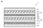
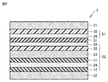
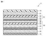
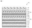
- the first adhesive layer 21 and the first protective film 32 are preferably in direct contact.
- Optical laminates 1 to 4 may have a surface functional layer between the first adhesive layer 21 and the first protective film 32 .
- the surface functional layer is preferably provided so as to be in direct contact with the first protective film 32 .
- the optical laminates 1 to 4 include surface functional layers, the surface functional layers and the first pressure-sensitive adhesive layer 21 may be in direct contact with each other.
- the thicknesses of the first retardation layer and the second retardation layer may each independently be 0.1 ⁇ m or more, 0.5 ⁇ m or more, 1 ⁇ m or more, or 2 ⁇ m. 10 ⁇ m or less, preferably 8 ⁇ m or less, or 5 ⁇ m or less.
- the adhesive composition As the adhesive composition, conventionally known adhesives with excellent optical transparency can be used without particular limitation. agent compositions can be used.
- the adhesive composition may also be an active energy ray-curable adhesive composition, a heat-curable adhesive composition, or the like.
- a pressure-sensitive adhesive composition using an acrylic resin as a base polymer which is excellent in transparency, adhesive strength, removability (reworkability), weather resistance, heat resistance, etc., is preferable.
- the pressure-sensitive adhesive layer preferably comprises a reaction product of a pressure-sensitive adhesive composition containing a (meth)acrylic resin, a cross-linking agent and a silane compound, and may contain other components.
- monomers other than the above include structural units derived from (meth)acrylic acid esters having an alicyclic structure in the molecule, structural units derived from styrene monomers, and vinyl monomers. structural units, structural units derived from monomers having multiple (meth)acryloyl groups in the molecule, structural units derived from (meth)acrylamide monomers, and the like. Other monomers may be used singly or in combination of two or more.
- the first adhesive layer may contain an ionic compound.
- the second pressure-sensitive adhesive layer preferably does not contain an ionic compound.
- the front plate is a plate-like body that can function as a layer for protecting the display element and the like of the display device and that can transmit light.
- the material and thickness of the front plate are not limited as long as it is a plate-like body that can transmit light.
- the front plate may be composed of only one layer, or may be composed of two or more layers. Examples of the front plate include a plate-like body made of resin (for example, a resin plate, a resin sheet, a resin film, etc.) and a plate-like body made of glass (for example, a glass plate, a glass film, etc.).
- the front panel can constitute the outermost surface of the display device.
- water-based adhesives include adhesives obtained by dissolving or dispersing polyvinyl alcohol-based resin in water.
- the method of drying when a water-based adhesive is used is not particularly limited. For example, a method of drying using a hot air dryer or an infrared ray dryer can be employed.
- Radically polymerizable curable compounds include, for example, (meth)acrylic compounds (compounds having one or more (meth)acryloyloxy groups in the molecule), and other radically polymerizable double bonds. or a combination thereof.
- Active energy ray-curable adhesives may optionally contain ion trapping agents, antioxidants, chain transfer agents, tackifiers, thermoplastic resins, fillers, flow control agents, plasticizers, antifoaming agents, and antistatic agents. Additives such as agents, leveling agents, solvents and the like can be included.
- the lamination was performed using a laminator, and the active energy ray-curable adhesive was applied so that the adhesive layer had a thickness of 3 ⁇ m after curing.
- the substrate layer / orientation layer / first cured layer (first retardation layer) / adhesive layer (second bonding layer) / second cured layer (second retardation layer) / orientation layer / A retardation layer with a substrate layer was obtained in which the substrate layers were laminated in this order.
- the total thickness of the first cured layer, the adhesive layer, and the second cured layer in the retardation layer with the substrate layer was 6 ⁇ m.
Landscapes
- Physics & Mathematics (AREA)
- Nonlinear Science (AREA)
- General Physics & Mathematics (AREA)
- Optics & Photonics (AREA)
- Chemical & Material Sciences (AREA)
- Crystallography & Structural Chemistry (AREA)
- Mathematical Physics (AREA)
- Spectroscopy & Molecular Physics (AREA)
- Organic Chemistry (AREA)
- Polarising Elements (AREA)
- Adhesive Tapes (AREA)
- Liquid Crystal (AREA)
Abstract
Description
〔1〕 第1粘着剤層、第1保護フィルム、偏光子、第1位相差層、及び、第2粘着剤層をこの順に含む光学積層体であって、
前記偏光子は、ヨウ素が吸着配向しているポリビニルアルコール系樹脂フィルムであり、
前記第1位相差層は、重合性液晶化合物の硬化物層を含み、
前記偏光子と前記第1粘着剤層との間に配置される層全体の温度40℃、相対湿度90%RHにおける透湿度をA1とし、
前記偏光子と前記第2粘着剤層との間に配置される層全体の温度40℃、相対湿度90%RHにおける透湿度をA2とするとき、下記式(I)の関係:
A1>A2 (I)
を満たし、かつ、
前記第1粘着剤層は、下記[a]及び[b]:
[a]前記第1粘着剤層の温度25℃、相対湿度80%RHにおける飽和水分率が0.5%以上である、
[b]前記第1粘着剤層がイオン性化合物を含む、
のうちの少なくとも一方を満たす、光学積層体。
〔2〕 前記透湿度A1と前記透湿度A2との比(A1/A2)は、1.1以上である、〔1〕に記載の光学積層体。
〔3〕 前記第1粘着剤層は、前記[a]を満たす、〔1〕又は〔2〕に記載の光学積層体。
〔4〕 さらに、前記第1粘着剤層と前記第1保護フィルムとの間に、表面機能層を有する、〔1〕~〔3〕のいずれかに記載の光学積層体。
〔5〕 さらに、前記偏光子と前記第1位相差層との間に、第2保護フィルムを有する、〔1〕~〔4〕のいずれかに記載の光学積層体。
〔6〕 前記第2保護フィルムと前記第1位相差層とは、第1貼合層を介して積層されている、〔5〕に記載の光学積層体。
〔7〕 さらに、前記第1位相差層と前記第2粘着剤層との間に、第2位相差層を有し、
前記第2位相差層は、重合性液晶化合物の硬化物層を含み、
前記第1位相差層と前記第2位相差層とは、第2貼合層を介して積層されている、〔1〕~〔6〕のいずれかに記載の光学積層体。
〔8〕 さらに、前記第2粘着剤層の前記第1位相差層側とは反対側に、金属層を有する、〔1〕~〔7〕のいずれかに記載の光学積層体。
〔9〕 さらに、前記第1粘着剤層の前記偏光子側とは反対側に、前面板を有する、〔1〕~〔8〕のいずれかに記載の光学積層体。
(光学積層体)
図1~図4は、本実施形態の光学積層体の一例を模式的に示す概略断面図である。本実施形態の光学積層体1~4は、第1粘着剤層21、第1保護フィルム32、偏光子31、第1位相差層11、及び第2粘着剤層22をこの順に有する。偏光子31は、ヨウ素が吸着配向しているポリビニルアルコール系樹脂フィルムである。第1位相差層11は、重合性液晶化合物の硬化物層を含む。
A1>A2 (I)
[式(I)において、
A1は、偏光子31と第1粘着剤層21との間に配置される層全体の温度40℃、相対湿度90%RHにおける透湿度である。
A2は、偏光子31と第2粘着剤層22との間に配置される層全体の温度40℃、相対湿度90%RHにおける透湿度である。]
[b]第1粘着剤層21がイオン性化合物を含む。
表示装置としては、有機EL表示装置、液晶表示装置等が挙げられる。表示装置はフレキシブルディスプレイであってもよい。
(偏光子)
無偏光の光を入射させたとき、吸収軸に直交する振動面をもつ直線偏光を透過させる性質を有する。偏光子は、ヨウ素が吸着配向しているポリビニルアルコール系樹脂フィルム(以下、「PVA系フィルム」ということがある。)である。
偏光子は、その各面に各々、第1保護フィルム及び第2保護フィルムを積層して偏光板とすることができる。偏光板は、第1保護フィルムを有し、第2保護フィルムを有していなくてもよい。
第1保護フィルム及び第2保護フィルムとしては、例えば、透明性、機械的強度、熱安定性、水分遮断性、等方性、延伸性等に優れる熱可塑性樹脂から形成されたフィルムが用いられる。熱可塑性樹脂の具体例としては、トリアセチルセルロース等のセルロース樹脂;ポリエチレンテレフタレート、ポリエチレンナフタレート等のポリエステル樹脂;ポリエーテルスルホン樹脂;ポリスルホン樹脂;ポリカーボネート樹脂;ナイロンや芳香族ポリアミド等のポリアミド樹脂;ポリイミド樹脂;ポリエチレン、ポリプロピレン、エチレン・プロピレン共重合体等のポリオレフィン樹脂;シクロ系及びノルボルネン構造を有する環状ポリオレフィン樹脂(ノルボルネン系樹脂ともいう);(メタ)アクリル樹脂;ポリアリレート樹脂;ポリスチレン樹脂;ポリビニルアルコール樹脂、並びにこれらの混合物を挙げることができる。第1保護フィルム及び第2保護フィルムの樹脂組成は同一であってもよいし、異なっていてもよい。なお、本明細書において「(メタ)アクリル」とは、アクリル又はメタクリルのいずれでもよいことを意味する。(メタ)アクリレート等の「(メタ)」も同様の意味である。
第1位相差層及び第2位相差層は、それぞれ重合性液晶化合物が重合硬化した硬化物層を含む。第1位相差層及び第2位相差層はそれぞれ、重合性液晶化合物を所望の方向に配向させる配向規制力を有する配向層を含んでいてもよい。
第1粘着剤層及び第2粘着剤層は、粘着剤組成物を用いて形成された粘着剤層である。
粘着剤組成物又は粘着剤組成物の反応生成物は、それ自体を金属層等の被着体に張り付けることで接着性を発現するものであり、いわゆる感圧型接着剤と称されるものである。また、後述する活性エネルギー線硬化型粘着剤組成物を用いて形成された粘着剤層は、活性エネルギー線を照射することにより、架橋度や接着力を調整することができる。
極性官能基としては、遊離カルボキシル基、水酸基、アミノ基、エポキシ基をはじめとする複素環基等を挙げることができる。
他の単量体としては、芳香環を有する(メタ)アクリル酸系化合物を挙げることができる。芳香環を有する(メタ)アクリル酸系化合物としては、アリールオキシアルキル基を有する(メタ)アクリル酸エステルが挙げられ、具体的には、(メタ)アクリル酸2-フェノキシエチル、(メタ)アクリル酸2-(2-フェノキシエトキシ)エチル、エチレンオキサイド変性ノニルフェノールの(メタ)アクリル酸エステル、(メタ)アクリル酸2-(o-フェニルフェノキシ)エチル等を含む。フェノキシエチル基含有(メタ)アクリル酸エステルは、1種のみを単独で用いてもよいし、2種以上を併用してもよい。中でも、フェノキシエチル基含有(メタ)アクリル酸エステルは、(メタ)アクリル酸2-フェノキシエチル、(メタ)アクリル酸2-(o-フェニルフェノキシ)エチル、及び(メタ)アクリル酸2-(2―フェノキシエトキシ)エチル等が挙げられる。
金属層は、タッチパネルのタッチセンサを構成するための導電層として用いることができる。金属層は、1種以上の金属によって形成された層である。金属層は、その表面に不動態被膜(酸化被膜)が形成されていてもよいものとする。金属層は単層構造であってもよく多層構造であってもよい。なお、不動態被膜は1つの層としては数えないものとする。
前面板は、表示装置の表示素子等を保護するための層として機能することができ、光を透過可能な板状体である。前面板は、光を透過可能な板状体であれば、材料及び厚みは限定されることはない。前面板は、1層のみから構成されてもよく、2層以上から構成されてもよい。前面板としては、樹脂製の板状体(例えば樹脂板、樹脂シート、樹脂フィルム等)、ガラス製の板状体(例えばガラス板、ガラスフィルム等)が挙げられる。前面板は、表示装置の最表面を構成することができる。また、前面板は、樹脂フィルム、又は、樹脂フィルムの少なくとも一方の面にハードコート層を設けて硬度をより向上させたハードコート層付き樹脂フィルムであってもよい。ハードコート層付き樹脂フィルムを用いる場合、ハードコート層は表示装置の最表面に配置されるように設けることが好ましい。また、前面板は、ブルーライトカット機能、視野角調整機能等を有するものであってもよい。
第1貼合層、第2貼合層、第3貼合層、及び第4貼合層(以下、これらをまとめて「貼合層」ということがある。)は、それぞれ独立して、粘着剤層又は接着剤層である。
冷却管、窒素導入管、温度計、及び撹拌機を備えた反応容器に、表1に示すモノマー組成(モノマー全量を100質量%としたときの質量%)を含み、酢酸エチルで希釈したモノマー混合物を仕込み、窒素ガスで反応容器内の空気を置換して酸素不含としながら内温を55℃に上げた。その後、アゾビスイソブチロニトリル(重合開始剤)を酢酸エチルに溶かした溶液を全量添加した。重合開始剤を添加した後、1時間この温度で保持し、次いで内温を54~56℃に保ちながら酢酸エチルを反応容器内へ連続的に加え、(メタ)アクリル系樹脂の濃度が35質量%となった時点で酢酸エチルの添加を止め、さらに酢酸エチルの添加開始から12時間経過するまでこの温度で保温した。最後に酢酸エチルを加えて(メタ)アクリル系樹脂の濃度が20質量%となるように調節し、(メタ)アクリル系樹脂の酢酸エチル溶液を調製した。
撹拌機、温度計、還流冷却器、滴下装置及び窒素導入管を備えた反応容器に、アクリル酸n-ブチル98.5質量部、アクリル酸1.0質量部、アクリル酸2-ヒドロキシエチル0.5質量部、酢酸エチル200質量部、及び2,2'-アゾビスイソブチロニトリル0.08質量部を仕込み、上記反応容器内の空気を窒素ガスで置換した。窒素雰囲気下で撹拌しながら、反応溶液を60℃に昇温し、6時間反応させた後、室温まで冷却した。得られた溶液において(メタ)アクリル系樹脂の生成を確認した。また、得られた溶液の一部の重量平均分子量(Mw)及び数平均分子量(Mn)を上記の手順で測定した。重量平均分子量(Mw)及びMw/Mnの結果を表1に示す。

BA :アクリル酸ブチル
MA :アクリル酸メチル
PEA :アクリル酸2-フェノキシエチル
HEA :アクリル酸2-ヒドロキシエチル
AA :アクリル酸
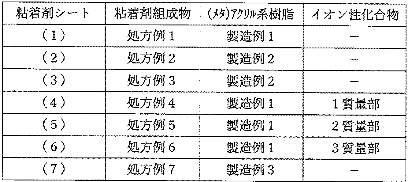
製造例1で得られた(メタ)アクリル系樹脂の固形分100質量部に対し、架橋剤として東ソー(株)から入手した「コロネートL」(トリレンジイソシアネートのトリメチロールプロパンアダクト体の酢酸エチル溶液:固形分濃度75質量%)0.5質量部、シラン化合物として信越化学工業(株)から入手した「KBM-403」(3-グリシドキシプロピルトリメトキシシラン)を0.5質量部添加し、処方例4~6については、イオン性化合物としてのN-オクチル-4-メチルピリジニウム6フッ化リンを、表2に記載した量で混合し、さらに固形分濃度が15質量%となるように酢酸エチルを添加して粘着剤組成物の溶液を調製した。架橋剤の配合量(質量部)は固形分換算量である。
製造例2で得られた(メタ)アクリル系樹脂の固形分100質量部に対し、架橋剤として東ソー(株)から入手した「コロネートL」(トリレンジイソシアネートのトリメチロールプロパンアダクト体の酢酸エチル溶液:固形分濃度75質量%)0.2質量部、シラン化合物として信越化学工業(株)から入手した「KBM-403」(3-グリシドキシプロピルトリメトキシシラン)を0.5質量部添加し、さらに固形分濃度が15質量%となるように酢酸エチルを添加して粘着剤組成物の溶液を調製した。架橋剤の配合量(質量部)は固形分換算量である。
架橋剤の配合量を1.0質量部にしたこと以外は、処方例2と同様にして粘着剤組成物の溶液を調製した。
製造例3で得られた(メタ)アクリル系樹脂100質量部(固形分換算値;以下同じ)と、イソシアネート系架橋剤としてのトリメチロールプロパン変性トリレンジイソシアネート(東ソー株式会社製、商品名「コロネートL」)0.30質量部と、シランカップリング剤としての3-グリシドキシプロピルトリメトキシシラン(信越化学工業株式会社製,商品名「KBM403」)0.30質量部とを混合し、十分に撹拌して、酢酸エチルで希釈することにより、粘着剤組成物の塗工溶液を得た。
処方例1~6で調製した粘着剤組成物を、離型処理が施されたポリエチレンテレフタレートフィルムからなるセパレートフィルム〔リンテック(株)から入手した「PLR-382190」〕の離型処理面に、アプリケータを用いて乾燥後の厚みが25μmとなるように塗布し、温度100℃で1分間乾燥して粘着剤層を作製した。得られた粘着剤層のセパレートフィルム側とは反対側の面に、離型処理が施されたポリエチレンテレフタレートフィルムからなるセパレートフィルム〔リンテック(株)から入手した「PLR-251130」〕の離型処理面を貼り合わせ、粘着剤シート(1)~(6)を作製した。
処方例7で調製した粘着剤組成物を、セパレートフィルム〔リンテック(株)から入手した「SP-PLR382190」〕の離型処理面に、アプリケータを用いて乾燥後の厚みが25μmとなるように塗布し、温度100℃で1分間乾燥して粘着剤層を作製した。
得られた粘着剤層のセパレートフィルム側とは反対側の面に、もう1枚のセパレートフィルム〔リンテック(株)から入手した「SP-PLR381031」〕の離型処理面を貼り合わせ、粘着剤シート(7)を作製した。
(偏光子の作製)
厚み30μmのポリビニルアルコール系樹脂フィルム(平均重合度約2400、ケン化度99.9モル%以上)を乾式延伸により約5倍に縦一軸延伸し、さらに緊張状態を保ったまま、温度60℃の純水に1分間浸漬した後、ヨウ素/ヨウ化カリウム/水の質量比が0.05/5/100である温度28℃の水溶液に60秒間浸漬した。その後、ヨウ化カリウム/ホウ酸/水の質量比が8.5/8.5/100である温度72℃の水溶液に300秒間浸漬した。引き続き温度26℃の純水で20秒間洗浄した後、温度65℃で乾燥処理を行って、ポリビニルアルコール系樹脂フィルムにヨウ素が吸着配向している、厚み12μmの偏光子を得た。
水100質量部に対し、カルボキシル基変性ポリビニルアルコール〔株式会社クラレ製の「KL-318」〕を3質量部溶解して、ポリビニルアルコール水溶液を調製した。得られた水溶液に水溶性ポリアミドエポキシ樹脂〔田岡化学工業株式会社製の「スミレーズレジン650(30)」、固形分濃度30質量%〕を、水100質量部に対し、1.5質量部の割合で混合して、水系接着剤を得た。
上記で得た偏光子の一方の面に、上記で得た水系接着剤を塗布し、ハードコート層(以下、「HC層」ということがある。)を有するトリアセチルセルロールフィルム(以下、「TACフィルム」ということがある。)を積層し、偏光子の他方の面に、上記で得た水系接着剤を用いて、TACフィルムを積層して、温度80℃で5分間乾燥することにより、偏光子の両面に保護フィルムを有する偏光板を得た。偏光板の層構造は、HC層(表面機能層)/TACフィルム(第1保護フィルム)/水系接着剤層(第3貼合層)/偏光子/水系接着剤層(第4貼合層)/TACフィルム(第2保護フィルム)であった。偏光板のHC層上に、基材フィルム上に粘着剤層を有するプロテクトフィルムを積層し、プロテクトフィルム付き偏光板(以下、「PF付き偏光板」ということがある。)を得た。
透明樹脂で形成された基材層上に、配向層形成用組成物を塗布し乾燥することにより、λ/2配向処理をした。次いで、配向層上に、ディスコチック重合性液晶化合物を含む液晶層形成用組成物を塗布し、加熱及びUV照射をして重合性液晶化合物の配向を固定化することにより、基材層の配向層上に、厚み2μmの第1硬化物層(λ/2位相差層)を形成した。
透明樹脂で形成された基材層上のラビング処理された配向層に、棒状のネマチック重合性液晶化合物を含む液晶層形成用組成物を塗布し、屈折率異方性を保持した状態で固化することにより、基材層の配向層上に、厚み1μmの第2硬化物層(λ/4位相差層)を形成した。
基材層上の第1硬化物層の表面、及び、基材層上の第2硬化物層の表面のそれぞれにコロナ処理を施した。第1硬化物層及び第2硬化物層の遅相軸のなす角度が60°となるように、それぞれのコロナ処理面どうしを、活性エネルギー線硬化型接着剤を用いて貼合した。その後、第2硬化物層側から、紫外線照射装置〔フュージョンUVシステムズ(株)製〕を用い、積算光量400mJ/cm2(UV-B)で紫外線照射を行って活性エネルギー線硬化型接着剤を硬化させて接着剤層を形成した。貼合は、ラミネータを用いて行い、活性エネルギー線硬化型接着剤は、硬化後の接着剤層の厚みが3μmとなるように塗布した。これにより、基材層/配向層/第1硬化物層(第1位相差層)/接着剤層(第2貼合層)/第2硬化物層(第2位相差層)/配向層/基材層がこの順に積層された基材層付き位相差層を得た。基材層付き位相差層のうち、第1硬化物層、接着剤層、及び第2硬化物層の総厚みは6μmであった。
上記で得た基材層付き位相差層の第1硬化物層側の基材層及び配向層を剥離して露出した第1硬化物層と、上記で得たPF付き偏光板の偏光板側とを、厚み5μmのアクリル系粘着剤層(第1貼合層、貯蔵弾性率:125,500Pa)を用いて貼合した。第1硬化物層と偏光板との貼合は、第1硬化物層の遅相軸と偏光子の透過軸とのなす角度が15°となるように行った。次いで、第2硬化物層側の基材層及び配向層を剥離して露出した第2硬化物層に、厚み15μmの粘着剤層(第2粘着剤層、貯蔵弾性率:25,500Pa)及びセパレートフィルムをこの順に積層して積層体(1)を得た。第1貼合層及び第2粘着剤層の貯蔵弾性率は、次の手順で測定した。
第1貼合層及び第2粘着剤層を構成する粘着剤層を各々、厚みが0.2mmになるように複数枚積層した。積層した粘着剤層を、直径8mmの円柱体となるように打ち抜き、これを貯蔵弾性率の測定用サンプルとした。測定用サンプルについて、JIS K7244-6に準拠し、粘弾性測定装置(Physica社製、MCR300)を用いてねじりせん断法により、以下の条件で貯蔵弾性率[Pa]を測定した。
<測定条件>
・ノーマルフォースFN:1N
・歪みγ:1%
・周波数:1Hz
・温度:25℃
粘着剤シート(1)に代えて粘着剤シート(2)~(7)を用いて積層粘着剤層を得、この積層粘着剤層を用いたこと以外は、実施例1と同様にして光学積層体(2)~(7)を得た。
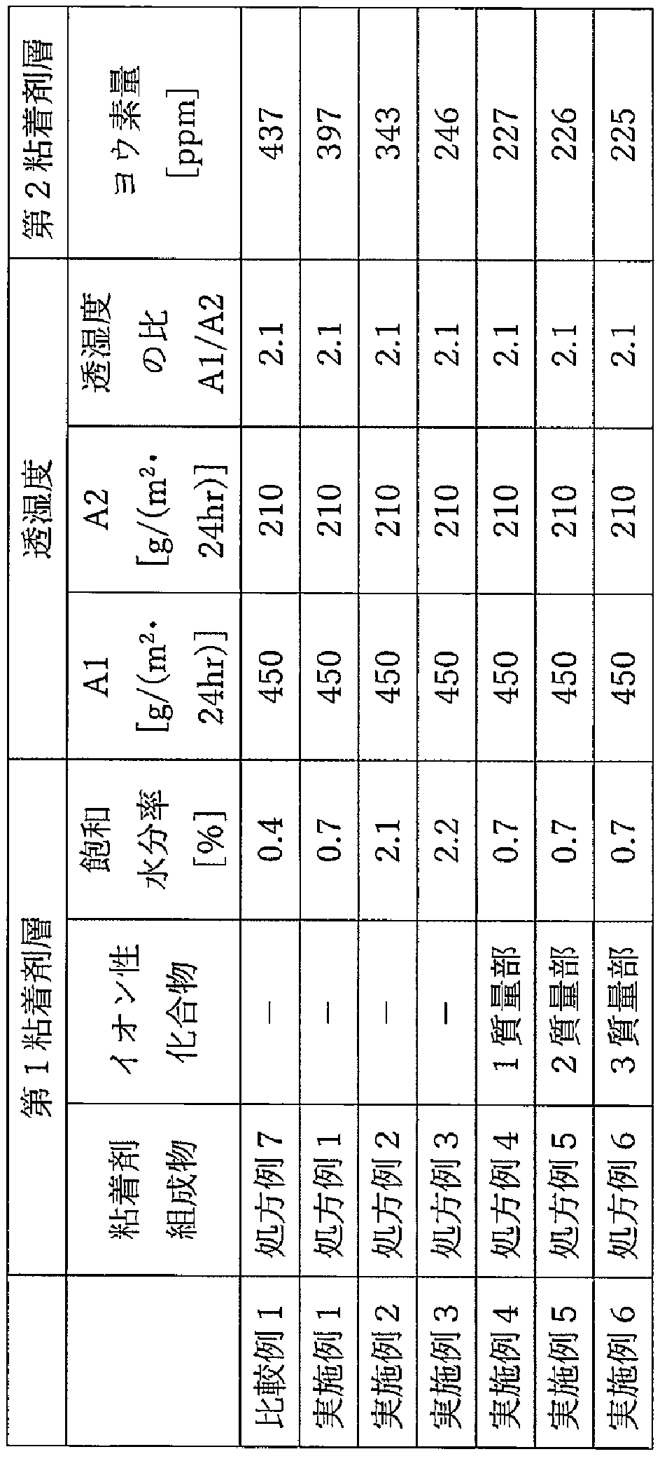
光学積層体(1)~(7)の偏光子と第1粘着剤層との間の積層構造部分S1(HC層/TACフィルム/水系接着剤層)の透湿度A1、及び、偏光子と第2粘着剤層との間の積層構造部分S2(水系接着剤層/TACフィルム/アクリル系粘着剤層/第1硬化物層/接着剤層/第2硬化物層)の透湿度A2を次の手順で決定した。
上記で作製した粘着剤シート(1)~(7)の粘着剤層(厚み:25μm)の各々を、下記の保管条件(1)で保管した後、下記の保管条件(2)で保管した。水分吸脱着測定装置IGA Sorp(Hiden Isochema製)を用いて各保管条件後の粘着剤層の質量を測定し、下式に基づいて粘着剤層の温度25℃、相対湿度80%RHにおける飽和水分率を求めた。結果を表3に示す。
保管条件(1):温度25℃、乾燥雰囲気下、保管時間24hr
保管条件(2):温度25℃、相対湿度80%RH、保管時間15hr
飽和水分率[%]=[(保管条件(2)後の質量)-(保管条件(1)後の質量)]/(保管条件(1)後の質量)
実施例及び比較例で得た光学積層体(1)~(7)を25mm×50mmの大きさに裁断し、第1粘着剤層側のセパレートフィルムを剥がし、露出した第1粘着剤層を無アルカリガラスに貼合して試験片を作製した。試験片を、温度85℃、相対湿度85%RHのオーブン中で240時間保管した後、第2粘着剤層側のセパレートフィルムを剥がし、第2粘着剤層の粘着剤を掻き取った。下記の条件で行った酸化燃焼イオンクロマトグラフ法により、掻き取った粘着剤に含まれるヨウ素量[ppm]を測定した。結果を表3に示す。
<試料燃焼>
・装置:株式会社三菱化学アナリテック製 AQF-2100H
・燃焼条件:燃焼温度を1100℃とし、ガス流量は、アルゴン流量を200mL/分、酸素流量を400mL/分、加湿空気流量を100mL/分とした。
<イオンクロオマトグラフ>
・装置:サーモフィッシャーサイエンティフィック社製 Integrion
・カラム:サーモフィッシャーサイエンティフィック社製 IonPac AS19
・測定条件:溶離液をKOH水溶液グラジエント、流速を1.0mL/分、注入量を100μL、測定モードをサプレッサ式、検出器を電気伝導度検出器とした。
Claims (9)
- 第1粘着剤層、第1保護フィルム、偏光子、第1位相差層、及び、第2粘着剤層をこの順に含む光学積層体であって、
前記偏光子は、ヨウ素が吸着配向しているポリビニルアルコール系樹脂フィルムであり、
前記第1位相差層は、重合性液晶化合物の硬化物層を含み、
前記偏光子と前記第1粘着剤層との間に配置される層全体の温度40℃、相対湿度90%RHにおける透湿度をA1とし、
前記偏光子と前記第2粘着剤層との間に配置される層全体の温度40℃、相対湿度90%RHにおける透湿度をA2とするとき、下記式(I)の関係:
A1>A2 (I)
を満たし、かつ、
前記第1粘着剤層は、下記[a]及び[b]:
[a]前記第1粘着剤層の温度25℃、相対湿度80%RHにおける飽和水分率が0.5%以上である、
[b]前記第1粘着剤層がイオン性化合物を含む、
のうちの少なくとも一方を満たす、光学積層体。 - 前記透湿度A1と前記透湿度A2との比(A1/A2)は、1.1以上である、請求項1に記載の光学積層体。
- 前記第1粘着剤層は、前記[a]を満たす、請求項1又は2に記載の光学積層体。
- さらに、前記第1粘着剤層と前記第1保護フィルムとの間に、表面機能層を有する、請求項1~3のいずれか1項に記載の光学積層体。
- さらに、前記偏光子と前記第1位相差層との間に、第2保護フィルムを有する、請求項1~4のいずれか1項に記載の光学積層体。
- 前記第2保護フィルムと前記第1位相差層とは、第1貼合層を介して積層されている、請求項5に記載の光学積層体。
- さらに、前記第1位相差層と前記第2粘着剤層との間に、第2位相差層を有し、
前記第2位相差層は、重合性液晶化合物の硬化物層を含み、
前記第1位相差層と前記第2位相差層とは、第2貼合層を介して積層されている、請求項1~6のいずれか1項に記載の光学積層体。 - さらに、前記第2粘着剤層の前記第1位相差層側とは反対側に、金属層を有する、請求項1~7のいずれか1項に記載の光学積層体。
- さらに、前記第1粘着剤層の前記偏光子側とは反対側に、前面板を有する、請求項1~8のいずれか1項に記載の光学積層体。
Priority Applications (2)
| Application Number | Priority Date | Filing Date | Title |
|---|---|---|---|
| CN202280020376.1A CN116981970A (zh) | 2021-05-10 | 2022-03-24 | 光学层叠体 |
| KR1020237040287A KR20240005766A (ko) | 2021-05-10 | 2022-03-24 | 광학 적층체 |
Applications Claiming Priority (2)
| Application Number | Priority Date | Filing Date | Title |
|---|---|---|---|
| JP2021079587A JP7680258B2 (ja) | 2021-05-10 | 2021-05-10 | 光学積層体 |
| JP2021-079587 | 2021-05-10 |
Publications (1)
| Publication Number | Publication Date |
|---|---|
| WO2022239508A1 true WO2022239508A1 (ja) | 2022-11-17 |
Family
ID=84029179
Family Applications (1)
| Application Number | Title | Priority Date | Filing Date |
|---|---|---|---|
| PCT/JP2022/014024 Ceased WO2022239508A1 (ja) | 2021-05-10 | 2022-03-24 | 光学積層体 |
Country Status (4)
| Country | Link |
|---|---|
| JP (1) | JP7680258B2 (ja) |
| KR (1) | KR20240005766A (ja) |
| CN (1) | CN116981970A (ja) |
| WO (1) | WO2022239508A1 (ja) |
Families Citing this family (1)
| Publication number | Priority date | Publication date | Assignee | Title |
|---|---|---|---|---|
| JP2024089227A (ja) * | 2022-12-21 | 2024-07-03 | 日東電工株式会社 | 位相差層付偏光板および位相差層付偏光板を含む画像表示装置 |
Citations (9)
| Publication number | Priority date | Publication date | Assignee | Title |
|---|---|---|---|---|
| JP2015004861A (ja) * | 2013-06-21 | 2015-01-08 | 日東電工株式会社 | 光学用粘着剤層、粘着剤層付光学フィルムおよび画像表示装置 |
| JP2015052765A (ja) * | 2013-09-09 | 2015-03-19 | 日東電工株式会社 | 透明導電膜用粘着剤層付偏光フィルム、積層体、及び、画像表示装置 |
| JP2016157077A (ja) * | 2015-02-26 | 2016-09-01 | 日東電工株式会社 | 粘着剤層付き偏光フィルム、及び画像表示装置 |
| JP2017075998A (ja) * | 2015-10-13 | 2017-04-20 | 日東電工株式会社 | 粘着シート、粘着剤層付き偏光板、および画像表示装置 |
| JP2018101117A (ja) * | 2016-12-21 | 2018-06-28 | 日東電工株式会社 | 画像表示装置 |
| JP2018205498A (ja) * | 2017-06-02 | 2018-12-27 | 日東電工株式会社 | 偏光フィルムおよび画像表示装置 |
| WO2019131218A1 (ja) * | 2017-12-26 | 2019-07-04 | 日東電工株式会社 | 粘着剤層付偏光板 |
| JP2019148734A (ja) * | 2018-02-28 | 2019-09-05 | 住友化学株式会社 | 円偏光板 |
| WO2021166659A1 (ja) * | 2020-02-17 | 2021-08-26 | 日東電工株式会社 | 粘着剤層付き偏光フィルム、および画像表示装置 |
Family Cites Families (6)
| Publication number | Priority date | Publication date | Assignee | Title |
|---|---|---|---|---|
| JP5049033B2 (ja) | 2007-03-08 | 2012-10-17 | 富士フイルム株式会社 | 液晶表示装置 |
| JP2010243863A (ja) | 2009-04-08 | 2010-10-28 | Sony Corp | 偏光板及び光装置 |
| JP6983497B2 (ja) | 2016-09-12 | 2021-12-17 | 日東電工株式会社 | 偏光フィルム、液晶パネルおよび液晶表示装置 |
| JP7236217B2 (ja) | 2018-02-08 | 2023-03-09 | 日東電工株式会社 | 粘着剤付き偏光板 |
| JP2019159311A (ja) * | 2018-03-12 | 2019-09-19 | 住友化学株式会社 | 偏光板およびそれを用いた画像表示装置 |
| JP7847937B2 (ja) | 2019-10-10 | 2026-04-20 | 日東電工株式会社 | 位相差層付偏光板およびそれを用いた有機エレクトロルミネセンス表示装置 |
-
2021
- 2021-05-10 JP JP2021079587A patent/JP7680258B2/ja active Active
-
2022
- 2022-03-24 KR KR1020237040287A patent/KR20240005766A/ko active Pending
- 2022-03-24 WO PCT/JP2022/014024 patent/WO2022239508A1/ja not_active Ceased
- 2022-03-24 CN CN202280020376.1A patent/CN116981970A/zh active Pending
Patent Citations (9)
| Publication number | Priority date | Publication date | Assignee | Title |
|---|---|---|---|---|
| JP2015004861A (ja) * | 2013-06-21 | 2015-01-08 | 日東電工株式会社 | 光学用粘着剤層、粘着剤層付光学フィルムおよび画像表示装置 |
| JP2015052765A (ja) * | 2013-09-09 | 2015-03-19 | 日東電工株式会社 | 透明導電膜用粘着剤層付偏光フィルム、積層体、及び、画像表示装置 |
| JP2016157077A (ja) * | 2015-02-26 | 2016-09-01 | 日東電工株式会社 | 粘着剤層付き偏光フィルム、及び画像表示装置 |
| JP2017075998A (ja) * | 2015-10-13 | 2017-04-20 | 日東電工株式会社 | 粘着シート、粘着剤層付き偏光板、および画像表示装置 |
| JP2018101117A (ja) * | 2016-12-21 | 2018-06-28 | 日東電工株式会社 | 画像表示装置 |
| JP2018205498A (ja) * | 2017-06-02 | 2018-12-27 | 日東電工株式会社 | 偏光フィルムおよび画像表示装置 |
| WO2019131218A1 (ja) * | 2017-12-26 | 2019-07-04 | 日東電工株式会社 | 粘着剤層付偏光板 |
| JP2019148734A (ja) * | 2018-02-28 | 2019-09-05 | 住友化学株式会社 | 円偏光板 |
| WO2021166659A1 (ja) * | 2020-02-17 | 2021-08-26 | 日東電工株式会社 | 粘着剤層付き偏光フィルム、および画像表示装置 |
Also Published As
| Publication number | Publication date |
|---|---|
| CN116981970A (zh) | 2023-10-31 |
| JP7680258B2 (ja) | 2025-05-20 |
| JP2022173715A (ja) | 2022-11-22 |
| TW202302355A (zh) | 2023-01-16 |
| KR20240005766A (ko) | 2024-01-12 |
Similar Documents
| Publication | Publication Date | Title |
|---|---|---|
| KR102665602B1 (ko) | 광학 적층체 및 액정 표시 장치 | |
| JP7642589B2 (ja) | 光学積層体 | |
| JP7731667B2 (ja) | 光学積層体 | |
| CN103930942B (zh) | 具有粘接剂层的图像显示装置用单元及使用了该单元的图像显示装置 | |
| KR102542169B1 (ko) | 점착제 조성물, 점착제층 및 점착제층이 구비된 광학 부재 | |
| US10054726B2 (en) | Polarizing plate and liquid crystal display comprising the same | |
| TWI708826B (zh) | 撓性積層體及具備其的圖像顯示裝置 | |
| JP7847949B2 (ja) | 偏光板および該偏光板を用いた画像表示装置 | |
| WO2021225114A1 (ja) | 画像表示装置 | |
| JP7680258B2 (ja) | 光学積層体 | |
| WO2022270402A1 (ja) | 表示装置 | |
| CN107177319B (zh) | 带粘合剂层的光学构件 | |
| JP2023003753A (ja) | 光学積層体及び表示装置 | |
| JP2022183013A (ja) | 光学積層体 | |
| TWI910290B (zh) | 偏光板套組及液晶面板 | |
| WO2022250025A1 (ja) | 光学積層体 | |
| CN117242376A (zh) | 光学层叠体 | |
| WO2023127471A1 (ja) | 円偏光板及び有機el表示装置 | |
| KR20240174494A (ko) | 점착제 조성물, 점착제층, 및 점착제 부착 편광판 | |
| KR20250018125A (ko) | 광학 적층체 및 이것을 포함하는 유기 el 표시 장치 | |
| KR20240129179A (ko) | 원편광판 | |
| JP2023070311A (ja) | 積層体及び表示装置 | |
| JP2023070310A (ja) | 積層体及び表示装置 |
Legal Events
| Date | Code | Title | Description |
|---|---|---|---|
| 121 | Ep: the epo has been informed by wipo that ep was designated in this application |
Ref document number: 22807213 Country of ref document: EP Kind code of ref document: A1 |
|
| WWE | Wipo information: entry into national phase |
Ref document number: 202280020376.1 Country of ref document: CN |
|
| ENP | Entry into the national phase |
Ref document number: 20237040287 Country of ref document: KR Kind code of ref document: A |
|
| NENP | Non-entry into the national phase |
Ref country code: DE |
|
| 122 | Ep: pct application non-entry in european phase |
Ref document number: 22807213 Country of ref document: EP Kind code of ref document: A1 |