WO2022239208A1 - 光半導体装置 - Google Patents
光半導体装置 Download PDFInfo
- Publication number
- WO2022239208A1 WO2022239208A1 PCT/JP2021/018294 JP2021018294W WO2022239208A1 WO 2022239208 A1 WO2022239208 A1 WO 2022239208A1 JP 2021018294 W JP2021018294 W JP 2021018294W WO 2022239208 A1 WO2022239208 A1 WO 2022239208A1
- Authority
- WO
- WIPO (PCT)
- Prior art keywords
- laser
- modulator
- temperature
- modulators
- semiconductor device
- Prior art date
- Legal status (The legal status is an assumption and is not a legal conclusion. Google has not performed a legal analysis and makes no representation as to the accuracy of the status listed.)
- Ceased
Links
Images






Classifications
-
- G—PHYSICS
- G02—OPTICS
- G02F—OPTICAL DEVICES OR ARRANGEMENTS FOR THE CONTROL OF LIGHT BY MODIFICATION OF THE OPTICAL PROPERTIES OF THE MEDIA OF THE ELEMENTS INVOLVED THEREIN; NON-LINEAR OPTICS; FREQUENCY-CHANGING OF LIGHT; OPTICAL LOGIC ELEMENTS; OPTICAL ANALOGUE/DIGITAL CONVERTERS
- G02F1/00—Devices or arrangements for the control of the intensity, colour, phase, polarisation or direction of light arriving from an independent light source, e.g. switching, gating or modulating; Non-linear optics
- G02F1/01—Devices or arrangements for the control of the intensity, colour, phase, polarisation or direction of light arriving from an independent light source, e.g. switching, gating or modulating; Non-linear optics for the control of the intensity, phase, polarisation or colour
- G02F1/0121—Operation of devices; Circuit arrangements, not otherwise provided for in this subclass
-
- G—PHYSICS
- G02—OPTICS
- G02F—OPTICAL DEVICES OR ARRANGEMENTS FOR THE CONTROL OF LIGHT BY MODIFICATION OF THE OPTICAL PROPERTIES OF THE MEDIA OF THE ELEMENTS INVOLVED THEREIN; NON-LINEAR OPTICS; FREQUENCY-CHANGING OF LIGHT; OPTICAL LOGIC ELEMENTS; OPTICAL ANALOGUE/DIGITAL CONVERTERS
- G02F1/00—Devices or arrangements for the control of the intensity, colour, phase, polarisation or direction of light arriving from an independent light source, e.g. switching, gating or modulating; Non-linear optics
- G02F1/01—Devices or arrangements for the control of the intensity, colour, phase, polarisation or direction of light arriving from an independent light source, e.g. switching, gating or modulating; Non-linear optics for the control of the intensity, phase, polarisation or colour
- G02F1/015—Devices or arrangements for the control of the intensity, colour, phase, polarisation or direction of light arriving from an independent light source, e.g. switching, gating or modulating; Non-linear optics for the control of the intensity, phase, polarisation or colour based on semiconductor elements having potential barriers, e.g. having a PN or PIN junction
-
- G—PHYSICS
- G02—OPTICS
- G02F—OPTICAL DEVICES OR ARRANGEMENTS FOR THE CONTROL OF LIGHT BY MODIFICATION OF THE OPTICAL PROPERTIES OF THE MEDIA OF THE ELEMENTS INVOLVED THEREIN; NON-LINEAR OPTICS; FREQUENCY-CHANGING OF LIGHT; OPTICAL LOGIC ELEMENTS; OPTICAL ANALOGUE/DIGITAL CONVERTERS
- G02F1/00—Devices or arrangements for the control of the intensity, colour, phase, polarisation or direction of light arriving from an independent light source, e.g. switching, gating or modulating; Non-linear optics
- G02F1/01—Devices or arrangements for the control of the intensity, colour, phase, polarisation or direction of light arriving from an independent light source, e.g. switching, gating or modulating; Non-linear optics for the control of the intensity, phase, polarisation or colour
- G02F1/015—Devices or arrangements for the control of the intensity, colour, phase, polarisation or direction of light arriving from an independent light source, e.g. switching, gating or modulating; Non-linear optics for the control of the intensity, phase, polarisation or colour based on semiconductor elements having potential barriers, e.g. having a PN or PIN junction
- G02F1/017—Structures with periodic or quasi periodic potential variation, e.g. superlattices, quantum wells
- G02F1/01708—Structures with periodic or quasi periodic potential variation, e.g. superlattices, quantum wells in an optical wavequide structure
-
- G—PHYSICS
- G02—OPTICS
- G02F—OPTICAL DEVICES OR ARRANGEMENTS FOR THE CONTROL OF LIGHT BY MODIFICATION OF THE OPTICAL PROPERTIES OF THE MEDIA OF THE ELEMENTS INVOLVED THEREIN; NON-LINEAR OPTICS; FREQUENCY-CHANGING OF LIGHT; OPTICAL LOGIC ELEMENTS; OPTICAL ANALOGUE/DIGITAL CONVERTERS
- G02F1/00—Devices or arrangements for the control of the intensity, colour, phase, polarisation or direction of light arriving from an independent light source, e.g. switching, gating or modulating; Non-linear optics
- G02F1/01—Devices or arrangements for the control of the intensity, colour, phase, polarisation or direction of light arriving from an independent light source, e.g. switching, gating or modulating; Non-linear optics for the control of the intensity, phase, polarisation or colour
- G02F1/015—Devices or arrangements for the control of the intensity, colour, phase, polarisation or direction of light arriving from an independent light source, e.g. switching, gating or modulating; Non-linear optics for the control of the intensity, phase, polarisation or colour based on semiconductor elements having potential barriers, e.g. having a PN or PIN junction
- G02F1/025—Devices or arrangements for the control of the intensity, colour, phase, polarisation or direction of light arriving from an independent light source, e.g. switching, gating or modulating; Non-linear optics for the control of the intensity, phase, polarisation or colour based on semiconductor elements having potential barriers, e.g. having a PN or PIN junction in an optical waveguide structure
-
- H—ELECTRICITY
- H01—ELECTRIC ELEMENTS
- H01S—DEVICES USING THE PROCESS OF LIGHT AMPLIFICATION BY STIMULATED EMISSION OF RADIATION [LASER] TO AMPLIFY OR GENERATE LIGHT; DEVICES USING STIMULATED EMISSION OF ELECTROMAGNETIC RADIATION IN WAVE RANGES OTHER THAN OPTICAL
- H01S5/00—Semiconductor lasers
- H01S5/005—Optical components external to the laser cavity, specially adapted therefor, e.g. for homogenisation or merging of the beams or for manipulating laser pulses, e.g. pulse shaping
- H01S5/0085—Optical components external to the laser cavity, specially adapted therefor, e.g. for homogenisation or merging of the beams or for manipulating laser pulses, e.g. pulse shaping for modulating the output, i.e. the laser beam is modulated outside the laser cavity
-
- H—ELECTRICITY
- H01—ELECTRIC ELEMENTS
- H01S—DEVICES USING THE PROCESS OF LIGHT AMPLIFICATION BY STIMULATED EMISSION OF RADIATION [LASER] TO AMPLIFY OR GENERATE LIGHT; DEVICES USING STIMULATED EMISSION OF ELECTROMAGNETIC RADIATION IN WAVE RANGES OTHER THAN OPTICAL
- H01S5/00—Semiconductor lasers
- H01S5/02—Structural details or components not essential to laser action
- H01S5/026—Monolithically integrated components, e.g. waveguides, monitoring photo-detectors, drivers
- H01S5/0265—Intensity modulators
-
- H—ELECTRICITY
- H01—ELECTRIC ELEMENTS
- H01S—DEVICES USING THE PROCESS OF LIGHT AMPLIFICATION BY STIMULATED EMISSION OF RADIATION [LASER] TO AMPLIFY OR GENERATE LIGHT; DEVICES USING STIMULATED EMISSION OF ELECTROMAGNETIC RADIATION IN WAVE RANGES OTHER THAN OPTICAL
- H01S5/00—Semiconductor lasers
- H01S5/04—Processes or apparatus for excitation, e.g. pumping, e.g. by electron beams
- H01S5/042—Electrical excitation ; Circuits therefor
-
- H—ELECTRICITY
- H01—ELECTRIC ELEMENTS
- H01S—DEVICES USING THE PROCESS OF LIGHT AMPLIFICATION BY STIMULATED EMISSION OF RADIATION [LASER] TO AMPLIFY OR GENERATE LIGHT; DEVICES USING STIMULATED EMISSION OF ELECTROMAGNETIC RADIATION IN WAVE RANGES OTHER THAN OPTICAL
- H01S5/00—Semiconductor lasers
- H01S5/06—Arrangements for controlling the laser output parameters, e.g. by operating on the active medium
- H01S5/0607—Arrangements for controlling the laser output parameters, e.g. by operating on the active medium by varying physical parameters other than the potential of the electrodes, e.g. by an electric or magnetic field, mechanical deformation, pressure, light, temperature
- H01S5/0612—Arrangements for controlling the laser output parameters, e.g. by operating on the active medium by varying physical parameters other than the potential of the electrodes, e.g. by an electric or magnetic field, mechanical deformation, pressure, light, temperature controlled by temperature
-
- H—ELECTRICITY
- H01—ELECTRIC ELEMENTS
- H01S—DEVICES USING THE PROCESS OF LIGHT AMPLIFICATION BY STIMULATED EMISSION OF RADIATION [LASER] TO AMPLIFY OR GENERATE LIGHT; DEVICES USING STIMULATED EMISSION OF ELECTROMAGNETIC RADIATION IN WAVE RANGES OTHER THAN OPTICAL
- H01S5/00—Semiconductor lasers
- H01S5/40—Arrangement of two or more semiconductor lasers, not provided for in groups H01S5/02 - H01S5/30
- H01S5/4012—Beam combining, e.g. by the use of fibres, gratings, polarisers, prisms
-
- H—ELECTRICITY
- H01—ELECTRIC ELEMENTS
- H01S—DEVICES USING THE PROCESS OF LIGHT AMPLIFICATION BY STIMULATED EMISSION OF RADIATION [LASER] TO AMPLIFY OR GENERATE LIGHT; DEVICES USING STIMULATED EMISSION OF ELECTROMAGNETIC RADIATION IN WAVE RANGES OTHER THAN OPTICAL
- H01S5/00—Semiconductor lasers
- H01S5/40—Arrangement of two or more semiconductor lasers, not provided for in groups H01S5/02 - H01S5/30
- H01S5/4025—Array arrangements, e.g. constituted by discrete laser diodes or laser bar
- H01S5/4087—Array arrangements, e.g. constituted by discrete laser diodes or laser bar emitting more than one wavelength
-
- H—ELECTRICITY
- H01—ELECTRIC ELEMENTS
- H01S—DEVICES USING THE PROCESS OF LIGHT AMPLIFICATION BY STIMULATED EMISSION OF RADIATION [LASER] TO AMPLIFY OR GENERATE LIGHT; DEVICES USING STIMULATED EMISSION OF ELECTROMAGNETIC RADIATION IN WAVE RANGES OTHER THAN OPTICAL
- H01S5/00—Semiconductor lasers
- H01S5/10—Construction or shape of the optical resonator, e.g. extended or external cavity, coupled cavities, bent-guide, varying width, thickness or composition of the active region
- H01S5/12—Construction or shape of the optical resonator, e.g. extended or external cavity, coupled cavities, bent-guide, varying width, thickness or composition of the active region the resonator having a periodic structure, e.g. in distributed feedback [DFB] lasers
Definitions
- the present disclosure relates to an optical semiconductor device.
- Patent Document 1 discloses a semiconductor laser device.
- This semiconductor laser device includes a plurality of DFB lasers with different oscillation wavelengths, a multiplexer that combines the outputs of the multiple DFB lasers, and an EA modulator that modulates the light output from the multiplexer.
- the semiconductor laser device also includes a temperature detector for measuring temperature, and a laser selection controller for selecting and switching a DFB laser to be operated from among the plurality of DFB lasers based on the temperature detected by the temperature detector. .
- An EML Electroabsorption modulated laser
- a DFB Distributed Feedback
- EA modulator Electroabsorption modulator
- the difference between the oscillation wavelength ⁇ DFB of the DFB laser and the absorption peak wavelength ⁇ EA of the EA modulator is called a separation amount ⁇ .
- the separation amount ⁇ is an important parameter that generally affects the performance of a communication LD (Laser Diode).
- the main characteristics of EML, the optical output and the extinction ratio, are generally in a trade-off relationship via ⁇ .
- the value of ⁇ is usually determined so as to optimize the balance between optical output and extinction ratio.
- the oscillation wavelength ⁇ DFB and the absorption peak wavelength ⁇ EA differ greatly in temperature dependence. Therefore, if the temperature of the device fluctuates, ⁇ may fluctuate greatly. Therefore, the balance between the optical output and the extinction ratio may be lost.
- Patent Document 1 the LD to be operated is switched according to the temperature. This allows the oscillation wavelength ⁇ DFB to follow a large temperature change in the absorption peak wavelength ⁇ EA.
- Patent Document 1 there is a risk that the range of values that the oscillation wavelength ⁇ DFB can take is widened. Therefore, if strict wavelength standards are required, there is a possibility that the semiconductor laser device of Patent Document 1 cannot be adopted.
- An object of the present disclosure is to obtain an optical semiconductor device capable of reducing the range in which the oscillation wavelength changes.
- An optical semiconductor device includes at least one laser, a plurality of EA modulators having an input side connected to the output of the laser and having mutually different absorption peak wavelengths, and an input side having the outputs of the plurality of EA modulators. and a waveguide connected to the output side, a temperature detector for detecting the temperature of the laser or the plurality of EA modulators, and the plurality of a selection control unit for switching an EA modulator to be operated among the EA modulators.
- the EA modulator to be operated among the plurality of EA modulators is switched according to the temperature. Therefore, the range in which the oscillation wavelength changes can be reduced.
- FIG. 1 is a block diagram showing the configuration of an optical semiconductor device according to Embodiment 1;
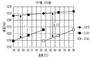
- FIG. 4 is a diagram showing how the oscillation wavelength ⁇ DFB and the absorption peak wavelength ⁇ EA change according to the first embodiment;
- FIG. 8 is a diagram showing how the oscillation wavelength ⁇ DFB and the absorption peak wavelength ⁇ EA change according to the first comparative example;
- FIG. 10 is a diagram showing how the oscillation wavelength ⁇ DFB and the absorption peak wavelength ⁇ EA change according to the second comparative example;
- FIG. 2 is a block diagram showing the configuration of an optical semiconductor device according to Embodiment 2;
- FIG. 11 is a diagram illustrating a lookup table according to Embodiment 2;
- FIG. FIG. 12 is a block diagram showing the configuration of an optical semiconductor device according to Embodiment 3;
- FIG. 12 is a block diagram showing the configuration of an optical semiconductor device according to Embodiment 4;
- 13 is a sectional view obtained by cutting FIG. 12 along a straight line AA.
- FIG. FIG. 13 is a cross-sectional view obtained by cutting FIG. 12 along a straight line BB.
- FIG. 1 is a block diagram showing the configuration of an optical semiconductor device 100 according to Embodiment 1.
- the optical semiconductor device 100 is an optical transmitter.
- the optical semiconductor device 100 is also called an uncooled EML optical transmitter.
- the optical semiconductor device 100 is equipped with an EML.
- EML is also called DFB laser with electro-absorption modulator.
- the optical semiconductor device 100 includes one laser 21 and a plurality of EA modulators 41 and 42 to which the output of the laser 21 is connected on the input side.
- Laser 21 is a DFB laser.
- the EA modulators 41 and 42 have different absorption peak wavelengths. Although two EA modulators 41 and 42 are shown in FIG. 1, three or more EA modulators may be provided.
- a branching filter 30 connects the laser 21 and a plurality of EA modulators 41 and 42 .
- the demultiplexer 30 demultiplexes the output light of the laser 21 and inputs it to a plurality of EA modulators 41 and 42 respectively.
- the multiplexer 50 has an input side connected to the outputs of the plurality of EA modulators 41 and 42 and an output side connected to a waveguide.
- MMI Multi-Mode Interference
- the laser 21, demultiplexer 30, EA modulators 41 and 42, multiplexer 50 and waveguide are monolithically integrated on the same substrate.
- a temperature detector 60 detects the temperature of the laser 21 or multiple EA modulators 41 , 42 .
- the temperature detector 60 may detect the temperature of the semiconductor optical integrated device 10, or may detect the temperature of the substrate on which the laser 21 and the plurality of EA modulators 41 and 42 are formed.
- the EA selection control unit 62 switches between the EA modulators 41 and 42 to be operated according to the detected temperature Tc of the temperature detector 60 .
- the EA driver 70 outputs a modulation signal for modulating the EA modulators 41 and 42 according to the signal 80 from the outside.
- the EA selection control section 62 outputs the modulated signal output from the EA driver 70 to one of the plurality of EA modulators 41 and 42 according to the detected temperature Tc.
- the EA selection control unit 62 selects the EA modulator 41 when the detected temperature Tc is -40°C to +25°C, and selects the EA modulator 42 when the detected temperature Tc is +25°C to +90°C.
- the oscillation wavelength ⁇ DFB of the laser 21 is designed to be 1310 nm at +25° C., for example.
- the absorption peak wavelength ⁇ EA1 of the EA modulator 41 is designed to be 1258 nm at +25° C., for example.
- the absorption peak wavelength is also called absorption edge wavelength.
- the absorption peak wavelength ⁇ EA2 of the EA modulator 42 is designed to be 1232 nm at +25° C., for example.
- the EA modulator 42 has a smaller absorption peak wavelength ⁇ EA than the EA modulator 41 at the same temperature.
- the EA selection control unit 62 operates the EA modulator 41 when the detected temperature Tc is lower than a predetermined threshold, and operates the EA modulator 42 when the detected temperature Tc is higher than the threshold.
- operating an EA modulator refers to outputting a modulated signal to the EA modulator.
- the threshold value of the detected temperature Tc is +25° C., for example.
- FIG. 2 is a diagram showing changes in the oscillation wavelength ⁇ DFB and the absorption peak wavelength ⁇ EA according to the first embodiment.
- the oscillation wavelength ⁇ DFB and the absorption peak wavelength ⁇ EA fluctuate, for example, by 0.1 nm/°C and 0.5 nm/°C, respectively, with temperature changes.
- the rate of variation of the absorption peak wavelength ⁇ EA with respect to temperature is greater than the rate of variation of the oscillation wavelength ⁇ DFB.
- the oscillation wavelength ⁇ DFB fluctuates in the range of 1303.5 to 1310 nm, with a fluctuation width of 6.5 nm.
- the absorption peak wavelength ⁇ EA1 fluctuates in the range of 1225.5 to 1258 nm with a fluctuation width of 32.5 nm.
- the separation amount ⁇ 1 which is the difference between the oscillation wavelength ⁇ DFB and the absorption peak wavelength ⁇ EA1, fluctuates in the range of 52 to 78 nm with a fluctuation width of 26 nm.
- ⁇ DFB fluctuates in the range of 1310 to 1316.5 nm, with a fluctuation width of 6.5 nm.
- the absorption peak wavelength ⁇ EA2 fluctuates in the range of 1232 to 1264.5 nm with a fluctuation width of 32.5 nm.
- the separation amount ⁇ 2 which is the difference between the oscillation wavelength ⁇ DFB and the absorption peak wavelength ⁇ EA2, fluctuates in the range of 52 to 78 nm with a fluctuation width of 26 nm.
- ⁇ DFB fluctuates in the range of 1303.5 to 1316.5 nm over the entire temperature range of ⁇ 40 to +90° C., with a fluctuation width of 13 nm.
- FIG. 3 is a diagram showing how the oscillation wavelength ⁇ DFB and the absorption peak wavelength ⁇ EA change according to the first comparative example.
- the first comparative example one EA modulator is provided, and the operating laser of two lasers with different oscillation wavelengths ⁇ DFB is switched according to the temperature.
- the absorption peak wavelength ⁇ EA of only one EA modulator is assumed to be fixed at 1245 nm at 25°C.
- the oscillation wavelength ⁇ DFB1 of the first laser is designed to be 1297 nm at 25°C.
- the oscillation wavelength ⁇ DFB2 of the second laser is designed to be 1323 nm at 25°C.
- the oscillation wavelength ⁇ DFB and the absorption peak wavelength ⁇ EA fluctuate by 0.1 nm/°C and 0.5 nm/°C, respectively, with temperature changes.
- the oscillation wavelength ⁇ DFB1 fluctuates in the range of 1290.5 to 1297 nm with a fluctuation width of 6.5 nm.
- the absorption peak wavelength ⁇ EA fluctuates in the range of 1212.5 to 1245 nm with a fluctuation width of 32.5 nm.
- the separation amount ⁇ 1 fluctuates in the range of 52 to 78 nm, and the fluctuation width is 26 nm.
- the oscillation wavelength ⁇ DFB2 fluctuates in the range of 1323 to 1329.5 nm with a fluctuation width of 6.5 nm.
- the absorption peak wavelength ⁇ EA fluctuates in the range of 1245 to 1277.5 nm with a fluctuation width of 32.5 nm.
- the separation amount ⁇ 2 fluctuates in the range of 52 to 78 nm, with a fluctuation width of 26 nm.
- the fluctuation width of the separation amount ⁇ in the entire temperature range of ⁇ 40 to +90° C. is 26 nm, which is the same as in the present embodiment.
- the variation width of the oscillation wavelength ⁇ DFB is 39 nm, which is three times that of the present embodiment.
- the absorption peak wavelength ⁇ EA changes more with temperature than the oscillation wavelength ⁇ DFB. Therefore, if the laser is switched so as to follow the temperature change of the absorption peak wavelength ⁇ EA, the fluctuation width of the oscillation wavelength ⁇ DFB becomes large. In this way, when switching the operating laser to suppress the fluctuation width of the distance ⁇ , the fluctuation width of the oscillation wavelength ⁇ DFB becomes large. Therefore, this embodiment is advantageous when particularly stringent wavelength standards are required.
- FIG. 4 is a diagram showing how the oscillation wavelength ⁇ DFB and the absorption peak wavelength ⁇ EA change according to the second comparative example.
- the second comparative example one laser and one EA modulator are provided.
- the fluctuation width of the separation amount ⁇ in the entire temperature range of ⁇ 40° C. to +90° C. is 52 nm, which is larger than that of the present embodiment.
- the variation width of the oscillation wavelength ⁇ DFB is 13 nm, which is the same as in the present embodiment.
- the range of possible values for the separation amount ⁇ is narrow in the present embodiment and the first comparative example. Further, the range of values taken by the oscillation wavelength ⁇ DFB is narrow in this embodiment and in the second comparative example. That is, it can be said that this embodiment is the best configuration among the above three modes.
- FIG. 5 is a flow chart explaining the operation of the optical semiconductor device 100 according to the first embodiment.
- FIG. 6 is a diagram illustrating a lookup table according to Embodiment 1.
- FIG. An algorithm for selecting and operating an EA modulator will be described with reference to FIGS.
- the temperature detector 60 is designed to output the detected temperature Tc, for example, in increments of 10°C.
- the EA selection control section 62 has a storage section.
- the EA selection control unit 62 stores in the storage unit a lookup table that associates discrete detected temperatures Tc with EA modulators to be selected.
- the EA selection control unit 62 reads the detected temperature Tc from the temperature detector 60 (step 1).
- the EA selection control unit 62 receives the detected temperature Tc from the temperature detector 60, it reads the EA modulator corresponding to the detected temperature Tc from the lookup table (step 2).
- EA1 indicates the EA modulator 41
- EA2 indicates the EA modulator .
- the EA selection control unit 62 selects and drives the EA modulator corresponding to the detected temperature Tc (step 3).
- the EA selection control section 62 may switch the driving voltage of the EA modulator according to the detected temperature Tc.
- the lookup table shown in FIG. 6 includes information on drive voltage corresponding to detected temperature Tc.
- the EA selection control section 62 may read the drive voltage corresponding to the detected temperature Tc and drive the EA modulator with the read drive voltage.
- the absolute value of the drive voltage is set to increase as the detected temperature Tc decreases.
- the temperature change of the absorption peak wavelength ⁇ EA follows the temperature change of the oscillation wavelength ⁇ DFB, which has a smaller temperature change than the absorption peak wavelength ⁇ EA. Therefore, compared to the first comparative example in which a plurality of lasers are switched, the range in which the oscillation wavelength ⁇ DFB changes can be reduced. Therefore, the optical semiconductor device 100 can be used even when strict wavelength standards are required.
- the EA selection control unit 62 operates the EA modulator 41 when the detected temperature Tc is within the first temperature range, and operates the EA modulator 42 when the detected temperature Tc is within the second temperature range.
- the first temperature range is -40 to +25°C and the second temperature range is +25 to +90°C.
- the range in which the absorption peak wavelength ⁇ EA1 of the EA modulator 41 changes in the first temperature range at least partially overlaps the range in which the absorption peak wavelength ⁇ EA2 of the EA modulator 42 changes in the second temperature range. ing.
- the fluctuation width of the separation amount ⁇ can be further reduced.
- the variation width of the separation amount ⁇ is smaller than that in the second comparative example, for example. It may be set as follows.
- FIG. 7 is a block diagram showing the configuration of an optical semiconductor device 200 according to the second embodiment.
- the optical semiconductor device 200 according to the present embodiment differs from the optical semiconductor device 100 in that a plurality of lasers 21 and 22 having different oscillation wavelengths ⁇ DFB are provided. Outputs of the plurality of lasers 21 and 22 are connected to the input sides of the plurality of EA modulators 41 and 42, respectively. Two lasers 21 and 22 are integrated in the semiconductor optical integrated device 10 .
- the optical semiconductor device 200 also includes a laser selection control section 64 and an EA selection control section 62 as selection control sections.
- the laser selection control unit 64 supplies a driving current to one of the plurality of lasers 21 and 22 according to the detected temperature Tc to operate it.
- the EA selection control unit 62 supplies a drive voltage to one of the plurality of EA modulators 41 and 42 according to the detected temperature Tc to operate it. In this manner, the selection control unit switches the laser to be operated among the plurality of lasers 21 and 22 and switches the EA modulator to be operated among the plurality of EA modulators according to the detected temperature Tc.
- Other configurations are the same as those of the first embodiment.
- FIG. 8 is a diagram showing changes in the oscillation wavelength ⁇ DFB and the absorption peak wavelength ⁇ EA according to the second embodiment.
- the EA selection control section 62 and the laser selection control section 64 the laser 21 and the EA modulator 41 are selected when the detected temperature Tc is -40°C to +25°C, and the laser 22 and the EA modulation are selected when the detected temperature Tc is +25°C to +90°C. device 42 is selected.
- the oscillation wavelength ⁇ DFB1 of the laser 21 is designed to be 1310 nm at -7.5°C, which is the center temperature of the temperature range -45 to +25°C.
- the oscillation wavelength ⁇ DFB2 of the laser 22 is designed to be 1310 nm at +57.5°C, which is the central temperature of the temperature range of +25 to +90°C.
- the absorption peak wavelength ⁇ EA1 of the EA modulator 41 is designed to be 1245 nm at -7.5°C, which is the center temperature of the temperature range -45 to +25°C.
- the absorption peak wavelength ⁇ EA2 of the EA modulator 42 is designed to be 1245 nm at +57.5°C, which is the center temperature of the temperature range +25 to +90°C.
- the laser 22 has a smaller oscillation wavelength ⁇ DFB than the laser 21 at the same temperature.
- the laser selection control unit 64 operates the laser 21 when the detected temperature Tc is lower than a predetermined threshold, and operates the laser 22 when the detected temperature Tc is higher than the threshold.
- the threshold is, for example, +25°C.
- the oscillation wavelength ⁇ DFB and the absorption peak wavelength ⁇ EA fluctuate, for example, by 0.1 nm/°C and 0.5 nm/°C, respectively, with temperature changes.
- the oscillation wavelength ⁇ DFB1 fluctuates in the range of 1306.75 to 1313.25 nm with a fluctuation width of 6.5 nm.
- the absorption peak wavelength ⁇ EA1 fluctuates in the range of 1228.75 to 1261.25 nm with a fluctuation width of 32.5 nm.
- the separation amount ⁇ 1 fluctuates in the range of 52 to 78 nm, with a fluctuation width of 26 nm.
- the oscillation wavelength ⁇ DFB2 fluctuates in the range of 1306.75 to 1313.25 nm with a fluctuation width of 6.5 nm.
- the absorption peak wavelength ⁇ EA2 fluctuates in the range of 1228.75 to 1261.25 nm with a fluctuation width of 32.5 nm.
- the separation amount ⁇ 2 fluctuates in the range of 52 to 78 nm, with a fluctuation width of 26 nm.
- the oscillation wavelength ⁇ DFB in the entire temperature range of -40 to +90°C fluctuates in the range of 1306.75 to 1313.25 nm, with a fluctuation width of 6.5 nm. Therefore, in this embodiment, the variation width of the oscillation wavelength ⁇ DFB can be suppressed to half that of the first embodiment. Further, the fluctuation width of the separation amount ⁇ is the same as in the first embodiment.
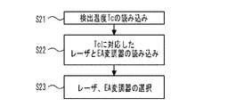
- FIG. 9 is a flow chart explaining the operation of the optical semiconductor device 200 according to the second embodiment.
- FIG. 10 is a diagram explaining a lookup table according to the second embodiment. 9 and 10 show an algorithm for selecting and operating the laser and EA modulator.
- the EA selection control unit 62 and the laser selection control unit 64 each store a lookup table that associates discrete detected temperatures Tc with selected lasers and EA modulators, as shown in FIG.
- the EA selection control unit 62 and the laser selection control unit 64 read the detected temperature Tc (step 21).
- the EA selection control section 62 and the laser selection control section 64 read the DFB laser and EA modulator corresponding to the detected temperature Tc from the lookup table (step 22).
- LD1 indicates the laser
- LD2 indicates the laser
- EA1 indicates the EA modulator 41
- EA2 indicates the EA modulator .
- the EA selection controller 62 and the laser selection controller 64 select and drive the laser and EA modulator corresponding to the detected temperature Tc (step 23).
- the laser selection control unit 64 may switch the laser driving current according to the detected temperature Tc.
- the EA modulator 41 may switch the driving voltage of the EA modulator according to the detected temperature Tc.
- the lookup table shown in FIG. 10 includes information on the laser drive current and the EA modulator drive voltage corresponding to the detected temperature Tc. In this manner, the laser selection control unit 64 may read the drive current corresponding to the detected temperature Tc and drive the laser with the read drive current.
- the EA selection control unit 62 may read a drive voltage corresponding to the detected temperature Tc and drive the EA modulator with the read drive voltage. In the example shown in FIG. 10, the drive current is set to increase as the detected temperature Tc increases.
- the absolute value of the drive voltage is set so as to increase as the detected temperature Tc decreases.
- the optical semiconductor device 200 can be used even when strict wavelength standards are required.
- the laser selection control unit 64 operates the laser 21 when the detected temperature Tc is within the first temperature range, and operates the laser 22 when the detected temperature Tc is within the second temperature range.
- the first temperature range is -40 to +25°C and the second temperature range is +25 to 90°C.
- the range in which the oscillation wavelength ⁇ DFB1 of the laser 21 changes in the first temperature range at least partially overlaps the range in which the oscillation wavelength ⁇ DFB2 of the laser 22 changes in the second temperature range. This makes it possible to reduce the variation width of the oscillation wavelength ⁇ DFB over the entire temperature range as compared with the first embodiment.
- the above shows an example of integrating two lasers and two EA modulators on the same substrate.
- three or more lasers with different oscillation wavelengths ⁇ DFB and three or more EA modulators with different absorption peak wavelengths ⁇ EA are integrated on the same substrate.
- One EA modulator may be selected. This narrows the temperature range that each laser and each EA modulator should cover. Therefore, it is possible to further reduce the fluctuation range of the separation amount ⁇ over the entire temperature range of -40 to +90°C.
- by providing three or more lasers or EA modulators it is possible to perform uncooled operation in a wider temperature range with the same fluctuation width of the distance ⁇ as in the case of two lasers and two EA modulators.
- the temperature at which the EA modulators 41 and 42 are switched and the temperature at which the lasers 21 and 22 are switched may be different.
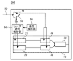
- FIG. 11 is a block diagram showing the configuration of an optical semiconductor device 300 according to the third embodiment.
- the optical semiconductor device 300 includes multiple EA modulators 41 and 42 and multiple lasers 21 and 22 . Further, the EA selection control unit 62 is not provided in this embodiment.
- Driving voltages are supplied from an EA driver 70 to the plurality of EA modulators 41 and 42, respectively.
- the EA driver 70 has an output terminal 71 that outputs a drive voltage.
- a plurality of EA modulators 41 and 42 are connected in parallel to an output terminal 71 of the EA driver 70 .
- Other configurations are the same as those of the second embodiment.
- the drive voltage of the EA driver is constantly supplied to the EA modulators 41 and 42 regardless of the detected temperature Tc. However, if there is no optical input from the rear laser, no optical signal is output from the EA modulator. Therefore, when the laser selection control unit 64 selects the laser 21 , the optical signal is output only from the EA modulator 41 . Similarly, when the laser selection controller 64 selects the laser 22 , only the EA modulator 42 outputs an optical signal. As described above, the selection control unit of the present embodiment switches the EA modulator to be operated indirectly by switching the laser to be operated.
- the EA selection control unit 62 is not provided in this embodiment. Therefore, the EA modulator can be switched with a less expensive configuration than the second embodiment. However, since two EA modulators 41 and 42 are connected in parallel to the output terminal 71 of one EA driver 70, the capacity is increased. Therefore, the modulation band may be inferior to that of the second embodiment.
- FIG. 12 is a block diagram showing the configuration of an optical semiconductor device 400 according to the fourth embodiment.
- the present embodiment differs from the third embodiment in that the other component is also used.
- the EA driver 70 outputs a positive-phase signal and a negative-phase signal as drive voltages.
- the positive phase signal is output from the output terminal 71 and the negative phase signal is output from the output terminal 72 .
- a normal phase signal is applied to one of the plurality of EA modulators 41 and 42, and a reverse phase signal is applied to the other.
- an EA modulator 41 receives a positive-phase signal and an EA modulator 42 receives a negative-phase signal.
- the polarities of the EA modulators 41 and 42 are the same, 1 and 0 of the optical signal output by the selected EA modulator are reversed. Therefore, the polarities of the EA modulators 41 and 42 should be reversed in advance.
- p-type electrode pad 41p and n-type electrode pad 41n of EA modulator 41 and p-type electrode pad 42p and n-type electrode pad 42n of EA modulator 42 are provided on the chip surface. be done.
- An output terminal 71 which is a positive phase output terminal, is connected to the p-type electrode pad 41p.
- the output terminal 72 which is the reverse phase output terminal, is connected to the n-type electrode pad 42n.
- FIG. 13 is a cross-sectional view obtained by cutting FIG. 12 along line AA.
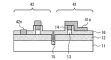
- FIG. 14 is a sectional view obtained by cutting FIG. 12 along line BB.
- Each of the EA modulators 41 and 42 includes a semi-insulating InP substrate 11, an n-type InP cladding layer 12, a light absorption layer 13, and a p-type InP cladding layer 14, which are sequentially laminated on the semi-insulating InP substrate 11. have.
- the EA modulators 41 and 42 are electrically separated by a trench 15 extending from the chip surface to the semi-insulating InP substrate 11.
- the upper surface of the n-type InP clad layer 12 and the side surfaces of the light absorption layer 13 and the p-type InP clad layer 14 are covered with a protective insulating film 16 .
- An opening in the protective insulating film 16 exposes the n-type InP clad layer 12 and the p-type InP clad layer 14 .
- P-type electrode pads 41p, 42p and n-type electrode pads 41n, 42n are formed on the chip surface.
- the p-type electrode pads 41p and 42p are connected to the p-type InP clad layer 14 through the openings of the protective insulating film 16. As shown in FIG.
- n-type electrode pads 41n and 42n are connected to the n-type InP clad layer 12 through the openings of the protective insulating film 16. As shown in FIG. In this manner, two EA modulators 41 and 42 with different polarities can be configured within the same chip.
Landscapes
- Physics & Mathematics (AREA)
- General Physics & Mathematics (AREA)
- Optics & Photonics (AREA)
- Nonlinear Science (AREA)
- Condensed Matter Physics & Semiconductors (AREA)
- Electromagnetism (AREA)
- Semiconductor Lasers (AREA)
- Optical Modulation, Optical Deflection, Nonlinear Optics, Optical Demodulation, Optical Logic Elements (AREA)
Abstract
Description
図1は、実施の形態1に係る光半導体装置100の構成を示すブロック図である。光半導体装置100は、光送信機である。光半導体装置100は、アンクールドEML光送信機とも呼ばれる。光半導体装置100はEMLを搭載している。EMLは、電界吸収型変調器付きDFBレーザとも呼ばれる。
図7は、実施の形態2に係る光半導体装置200の構成を示すブロック図である。本実施の形態に係る光半導体装置200で、互いに発振波長λDFBの異なる複数のレーザ21、22を備える点が光半導体装置100と異なる。複数のEA変調器41、42の入力側には、複数のレーザ21、22の出力がそれぞれ接続される。半導体光集積装置10には、2つのレーザ21、22が集積されている。
図11は、実施の形態3に係る光半導体装置300の構成を示すブロック図である。光半導体装置300は、複数のEA変調器41、42と複数のレーザ21、22を備える。また、本実施の形態ではEA選択制御部62が設けられない。複数のEA変調器41、42には、EAドライバ70からそれぞれ駆動電圧が供給される。EAドライバ70は、駆動電圧を出力する出力端子71を有する。EAドライバ70の出力端子71には、複数のEA変調器41、42が並列に接続される。他の構成は実施の形態2の構成と同様である。
図12は、実施の形態4に係る光半導体装置400の構成を示すブロック図である。実施の形態1~3では、EAドライバ70の差動出力端子の正相、逆相成分のうち、片方のみを利用している。これに対し本実施の形態では、もう一方の成分も利用する点が実施の形態3と異なる。
Claims (14)
- 少なくとも1つのレーザと、
入力側に前記レーザの出力が接続され、互いに吸収ピーク波長の異なる複数のEA変調器と、
入力側に前記複数のEA変調器の出力が接続され、出力側に導波路が接続された合波器と、
前記レーザまたは前記複数のEA変調器の温度を検出する温度検出器と、
前記温度検出器の検出温度に応じて、前記複数のEA変調器のうち動作させるEA変調器を切り替える選択制御部と、
を備えることを特徴とする光半導体装置。 - 前記複数のEA変調器は、第1EA変調器と第2EA変調器を含み、
前記第2EA変調器は、前記第1EA変調器よりも、同じ温度での前記吸収ピーク波長が小さく、
前記選択制御部は、前記検出温度が予め定められた閾値よりも低いとき前記第1EA変調器を動作させ、前記検出温度が前記閾値よりも高いとき前記第2EA変調器を動作させることを特徴とする請求項1に記載の光半導体装置。 - 前記選択制御部は、前記検出温度が第1温度範囲のとき前記第1EA変調器を動作させ、前記検出温度が第2温度範囲のとき前記第2EA変調器を動作させ、
前記第1温度範囲での前記第1EA変調器の前記吸収ピーク波長の変化する範囲は、前記第2温度範囲での前記第2EA変調器の前記吸収ピーク波長の変化する範囲と少なくとも一部が重複していることを特徴とする請求項2に記載の光半導体装置。 - 前記選択制御部は、前記検出温度に応じて前記複数のEA変調器の駆動電圧を切り替えることを特徴とする請求項1から3の何れか1項に記載の光半導体装置。
- 1つの前記レーザと、
前記レーザと前記複数のEA変調器とを接続し、前記レーザの出力光を分波して前記複数のEA変調器にそれぞれ入力させる分波器と、
を備えることを特徴とする請求項1から4の何れか1項に記載の光半導体装置。 - 互いに発振波長の異なる複数の前記レーザを備え、
前記複数のEA変調器の入力側には、前記複数のレーザの出力がそれぞれ接続され、
前記選択制御部は、前記検出温度に応じて前記複数のレーザのうち動作させるレーザを切り替えることを特徴とする請求項1から4の何れか1項に記載の光半導体装置。 - 前記複数のレーザは、第1レーザと第2レーザを含み、
前記第2レーザは、前記第1レーザよりも同じ温度での前記発振波長が小さく、
前記選択制御部は、前記検出温度が予め定められた閾値よりも低いとき前記第1レーザを動作させ、前記検出温度が前記閾値よりも高いとき前記第2レーザを動作させることを特徴とする請求項6に記載の光半導体装置。 - 前記選択制御部は、前記検出温度が第1温度範囲のとき前記第1レーザを動作させ、前記検出温度が第2温度範囲のとき前記第2レーザを動作させ、
前記第1温度範囲での前記第1レーザの前記発振波長の変化する範囲は、前記第2温度範囲での前記第2レーザの前記発振波長の変化する範囲と少なくとも一部が重複していることを特徴とする請求項7に記載の光半導体装置。 - 前記選択制御部は、前記検出温度に応じて前記複数のレーザの駆動電流を切り替えることを特徴とする請求項6から8の何れか1項に記載の光半導体装置。
- 前記選択制御部は、
前記検出温度に応じて、前記複数のレーザのうち1つに駆動電流を供給して動作させるレーザ選択制御部と、
前記検出温度に応じて、前記複数のEA変調器のうち1つに駆動電圧を供給して動作させるEA選択制御部と、
を備えることを特徴とする請求項6から9の何れか1項に記載の光半導体装置。 - 前記複数のEA変調器には、それぞれ駆動電圧が供給されることを特徴とする請求項6から9の何れか1項に記載の光半導体装置。
- 前記駆動電圧を出力する出力端子を有するEAドライバを備え、
前記EAドライバの前記出力端子には、前記複数のEA変調器が並列に接続されることを特徴とする請求項11に記載の光半導体装置。 - 前記駆動電圧として正相信号と逆相信号を出力するEAドライバを備え、
前記複数のEA変調器のうち第1EA変調器と第2EA変調器の一方には前記正相信号が印加され、
前記第1EA変調器と前記第2EA変調器の他方には前記逆相信号が印加されることを特徴とする請求項11に記載の光半導体装置。 - 前記第1EA変調器と前記第2EA変調器の前記一方のp型電極に、前記正相信号が印加され、
前記第1EA変調器と前記第2EA変調器の前記他方のn型電極に、前記逆相信号が印加されることを特徴とする請求項13に記載の光半導体装置。
Priority Applications (4)
| Application Number | Priority Date | Filing Date | Title |
|---|---|---|---|
| JP2021547290A JP6989068B1 (ja) | 2021-05-13 | 2021-05-13 | 光半導体装置 |
| CN202180097866.7A CN117280553A (zh) | 2021-05-13 | 2021-05-13 | 光半导体装置 |
| US18/260,599 US20240061279A1 (en) | 2021-05-13 | 2021-05-13 | Optical semiconductor device |
| PCT/JP2021/018294 WO2022239208A1 (ja) | 2021-05-13 | 2021-05-13 | 光半導体装置 |
Applications Claiming Priority (1)
| Application Number | Priority Date | Filing Date | Title |
|---|---|---|---|
| PCT/JP2021/018294 WO2022239208A1 (ja) | 2021-05-13 | 2021-05-13 | 光半導体装置 |
Publications (1)
| Publication Number | Publication Date |
|---|---|
| WO2022239208A1 true WO2022239208A1 (ja) | 2022-11-17 |
Family
ID=79239731
Family Applications (1)
| Application Number | Title | Priority Date | Filing Date |
|---|---|---|---|
| PCT/JP2021/018294 Ceased WO2022239208A1 (ja) | 2021-05-13 | 2021-05-13 | 光半導体装置 |
Country Status (4)
| Country | Link |
|---|---|
| US (1) | US20240061279A1 (ja) |
| JP (1) | JP6989068B1 (ja) |
| CN (1) | CN117280553A (ja) |
| WO (1) | WO2022239208A1 (ja) |
Families Citing this family (2)
| Publication number | Priority date | Publication date | Assignee | Title |
|---|---|---|---|---|
| JP7648836B1 (ja) | 2024-06-26 | 2025-03-18 | 三菱電機株式会社 | 光変調器集積半導体レーザ、光変調器集積半導体レーザの駆動方法、光モジュール、多値強度変調送受信装置、及び光回線終端装置 |
| JP7802250B1 (ja) * | 2025-03-13 | 2026-01-19 | 三菱電機株式会社 | 光変調器集積半導体レーザ及び光モジュール |
Citations (7)
| Publication number | Priority date | Publication date | Assignee | Title |
|---|---|---|---|---|
| JPH11220213A (ja) * | 1998-02-02 | 1999-08-10 | Nippon Telegr & Teleph Corp <Ntt> | 半導体光源装置、および、その制御方法 |
| US20030081878A1 (en) * | 2001-10-09 | 2003-05-01 | Joyner Charles H. | Transmitter photonic integrated circuit (TxPIC) chip with enhanced power and yield without on-chip amplification |
| JP2010239056A (ja) * | 2009-03-31 | 2010-10-21 | Opnext Japan Inc | 半導体素子及びその製造方法 |
| JP2013168500A (ja) * | 2012-02-15 | 2013-08-29 | Mitsubishi Electric Corp | 光半導体装置 |
| JP2017098342A (ja) * | 2015-11-19 | 2017-06-01 | 日本電信電話株式会社 | 波長多重光送信器 |
| WO2019111295A1 (ja) * | 2017-12-04 | 2019-06-13 | 三菱電機株式会社 | 電界吸収型変調器、光半導体装置及び光モジュール |
| JP2020109800A (ja) * | 2019-01-07 | 2020-07-16 | 三菱電機株式会社 | 半導体レーザー装置 |
Family Cites Families (5)
| Publication number | Priority date | Publication date | Assignee | Title |
|---|---|---|---|---|
| US6687278B1 (en) * | 1999-09-02 | 2004-02-03 | Agility Communications, Inc. | Method of generating an optical signal with a tunable laser source with integrated optical amplifier |
| JP4411938B2 (ja) * | 2003-11-04 | 2010-02-10 | 住友電気工業株式会社 | 変調器集積半導体レーザ、光変調システムおよび光変調方法 |
| CN1779545A (zh) * | 2004-11-18 | 2006-05-31 | 中国科学院半导体研究所 | 基于电吸收调制器光开关技术产生超短光脉冲的方法 |
| JP5395235B2 (ja) * | 2012-08-28 | 2014-01-22 | 日本オクラロ株式会社 | 波長可変光送信器および光送受信器 |
| CN208608991U (zh) * | 2018-09-13 | 2019-03-15 | 科大国盾量子技术股份有限公司 | 一种基于ea驱动电路的诱骗态制备装置 |
-
2021
- 2021-05-13 WO PCT/JP2021/018294 patent/WO2022239208A1/ja not_active Ceased
- 2021-05-13 CN CN202180097866.7A patent/CN117280553A/zh active Pending
- 2021-05-13 JP JP2021547290A patent/JP6989068B1/ja active Active
- 2021-05-13 US US18/260,599 patent/US20240061279A1/en active Pending
Patent Citations (7)
| Publication number | Priority date | Publication date | Assignee | Title |
|---|---|---|---|---|
| JPH11220213A (ja) * | 1998-02-02 | 1999-08-10 | Nippon Telegr & Teleph Corp <Ntt> | 半導体光源装置、および、その制御方法 |
| US20030081878A1 (en) * | 2001-10-09 | 2003-05-01 | Joyner Charles H. | Transmitter photonic integrated circuit (TxPIC) chip with enhanced power and yield without on-chip amplification |
| JP2010239056A (ja) * | 2009-03-31 | 2010-10-21 | Opnext Japan Inc | 半導体素子及びその製造方法 |
| JP2013168500A (ja) * | 2012-02-15 | 2013-08-29 | Mitsubishi Electric Corp | 光半導体装置 |
| JP2017098342A (ja) * | 2015-11-19 | 2017-06-01 | 日本電信電話株式会社 | 波長多重光送信器 |
| WO2019111295A1 (ja) * | 2017-12-04 | 2019-06-13 | 三菱電機株式会社 | 電界吸収型変調器、光半導体装置及び光モジュール |
| JP2020109800A (ja) * | 2019-01-07 | 2020-07-16 | 三菱電機株式会社 | 半導体レーザー装置 |
Also Published As
| Publication number | Publication date |
|---|---|
| JP6989068B1 (ja) | 2022-01-05 |
| US20240061279A1 (en) | 2024-02-22 |
| CN117280553A (zh) | 2023-12-22 |
| JPWO2022239208A1 (ja) | 2022-11-17 |
Similar Documents
| Publication | Publication Date | Title |
|---|---|---|
| US6516017B1 (en) | Multiwavelength semiconductor laser device with single modulator and drive method therefor | |
| US20160127070A1 (en) | Integrated two-channel spectral combiner and wavelength locker in silicon photonics | |
| JP6398969B2 (ja) | 集積光源及び光出力制御方法 | |
| JP6989068B1 (ja) | 光半導体装置 | |
| JP2009081512A (ja) | 光送信装置および設定値決定方法 | |
| de Valicourt et al. | Photonic integrated circuit based on hybrid III–V/silicon integration | |
| JP2009004903A (ja) | 光データリンク及び光出力制御方法 | |
| WO2014139103A1 (en) | Optical transceiver with isolated modulator contacts and/or inputs | |
| US9335495B2 (en) | Optical module | |
| JP2005326548A (ja) | 光変調装置、光送信装置及び光変調方法 | |
| US8724933B2 (en) | Optical device | |
| Saito et al. | Burst-tolerant tuning of reflection-type transversal filter laser with single active region | |
| JP5432043B2 (ja) | 光送信機 | |
| JP5109566B2 (ja) | 光送信機 | |
| JP6761390B2 (ja) | 半導体光集積素子 | |
| WO2016180146A1 (en) | Tunable wavelength-flattening element for switch carrying multiple wavelengths per lightpath | |
| JP5669665B2 (ja) | 光送受信器 | |
| JP5994230B2 (ja) | 光通信装置 | |
| JP2019033116A (ja) | 半導体光集積素子 | |
| US20050129077A1 (en) | Tunable electro-absorption modulator and tunable laser | |
| US7680164B1 (en) | Configurable laser driver with common anode and common cathode outputs | |
| JP2020109800A (ja) | 半導体レーザー装置 | |
| US20150303650A1 (en) | Low Cost Directly Modulated TWDM Burst Mode Laser | |
| JP4578989B2 (ja) | 光集積デバイス | |
| JP2006287144A (ja) | 光集積デバイス |
Legal Events
| Date | Code | Title | Description |
|---|---|---|---|
| ENP | Entry into the national phase |
Ref document number: 2021547290 Country of ref document: JP Kind code of ref document: A |
|
| 121 | Ep: the epo has been informed by wipo that ep was designated in this application |
Ref document number: 21941940 Country of ref document: EP Kind code of ref document: A1 |
|
| WWE | Wipo information: entry into national phase |
Ref document number: 18260599 Country of ref document: US |
|
| WWE | Wipo information: entry into national phase |
Ref document number: 202180097866.7 Country of ref document: CN |
|
| NENP | Non-entry into the national phase |
Ref country code: DE |
|
| 122 | Ep: pct application non-entry in european phase |
Ref document number: 21941940 Country of ref document: EP Kind code of ref document: A1 |