WO2022239154A1 - パワーモジュールおよび電力変換装置 - Google Patents
パワーモジュールおよび電力変換装置 Download PDFInfo
- Publication number
- WO2022239154A1 WO2022239154A1 PCT/JP2021/018070 JP2021018070W WO2022239154A1 WO 2022239154 A1 WO2022239154 A1 WO 2022239154A1 JP 2021018070 W JP2021018070 W JP 2021018070W WO 2022239154 A1 WO2022239154 A1 WO 2022239154A1
- Authority
- WO
- WIPO (PCT)
- Prior art keywords
- frame
- power module
- heat spreader
- insulating substrate
- semiconductor element
- Prior art date
- Legal status (The legal status is an assumption and is not a legal conclusion. Google has not performed a legal analysis and makes no representation as to the accuracy of the status listed.)
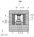
- Ceased
Links
Images





Classifications
-
- H—ELECTRICITY
- H10—SEMICONDUCTOR DEVICES; ELECTRIC SOLID-STATE DEVICES NOT OTHERWISE PROVIDED FOR
- H10W—GENERIC PACKAGES, INTERCONNECTIONS, CONNECTORS OR OTHER CONSTRUCTIONAL DETAILS OF DEVICES COVERED BY CLASS H10
- H10W76/00—Containers; Fillings or auxiliary members therefor; Seals
- H10W76/10—Containers or parts thereof
- H10W76/12—Containers or parts thereof characterised by their shape
Definitions
- the present disclosure relates to a power module and a power conversion device having a pressurizing section that pressurizes a bonding material.
- the power semiconductor elements mounted in the power module are exposed to high-temperature or high-temperature and low-temperature temperature cycles in order to switch the main current at high speed.
- each constituent member of the power module experiences a high stress load on the joints of each constituent member due to the difference in coefficient of linear expansion.
- solder joints using solder as a joint material are susceptible to cracking and deterioration.
- the present disclosure has been made to solve the above-described problems, and a power module with improved reliability is obtained by providing a pressure member between the lid and the wiring member to pressurize the joint. It is intended to
- a power module includes: a thermal diffusion part; an insulating substrate having a metal layer on the upper surface and the lower surface; the thermal diffusion part; a semiconductor element disposed above the semiconductor element and connected to the semiconductor element; a frame surrounding the insulating substrate and disposed in an outer peripheral region of the heat diffusion portion; and disposed on the upper surface side of the frame. a pressurizing portion disposed between the lid portion and the connection wiring portion to pressurize the semiconductor element through the connection wiring portion; and a fastening member for fastening the lid portion and the frame to the thermal diffusion portion. and a power module.
- the lid portion is arranged on the upper surface side of the frame
- the pressurizing portion is arranged between the lid portion and the connection wiring portion and presses the semiconductor element through the connection wiring portion
- the lid portion and a fastening member for fastening the frame body to the thermal diffusion part it is possible to pressurize the junction part that joins the semiconductor element and the metal layer on the upper surface of the insulating substrate, improving the reliability of the power module.
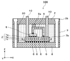
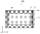
- FIG. 1 is a schematic plan view showing a power module according to Embodiment 1.
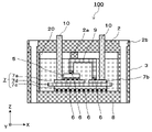
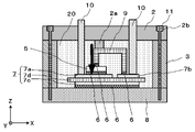
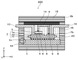
- FIG. 1 is a cross-sectional structural schematic diagram showing a power module according to Embodiment 1.
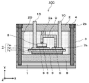
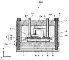
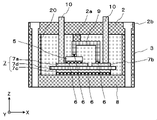
- FIG. 1 is a cross-sectional structural schematic diagram showing a power module according to Embodiment 1.
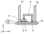
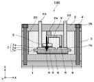
- FIG. 1 is a cross-sectional structural schematic diagram showing a power module according to Embodiment 1.
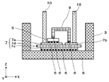
- FIG. 1 is a cross-sectional structural schematic diagram showing a power module according to Embodiment 1.
- FIG. 4 is a cross-sectional schematic diagram showing another power module in Embodiment 1.
- FIG. 4 is a cross-sectional schematic diagram showing another power module in Embodiment 1.
- FIG. 4 is a cross-sectional structural schematic diagram showing a manufacturing process of the power module in Embodiment 1;
- FIG. 4 is a cross-sectional structural schematic diagram showing a manufacturing process of the power module in Embodiment 1;
- FIG. 4 is a cross-sectional structural schematic diagram showing a manufacturing process of the power module in Embodiment 1;
- FIG. 4 is a cross-sectional structural schematic diagram showing a manufacturing process of the power module in Embodiment 1;
- FIG. 4 is a cross-sectional structural schematic diagram showing a manufacturing process of the power module in Embodiment 1;
- FIG. 4 is a cross-sectional structural schematic diagram showing a manufacturing process of the power module in Embodiment 1;
- FIG. 4 is a cross-sectional structural schematic diagram showing a manufacturing process of the power module in Embodiment 1;
- FIG. 4 is a cross-sectional structural schematic diagram showing a manufacturing process of the power module in Embodiment 1;
- FIG. 4 is a
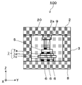
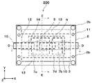
- FIG. 4 is a schematic plan view showing a power module according to Embodiment 2;
- FIG. 10 is a cross-sectional structural schematic diagram showing a power module according to Embodiment 2;
- FIG. 10 is a cross-sectional structural schematic diagram showing a power module according to Embodiment 2;
- FIG. 11 is a schematic plan view showing a power module according to Embodiment 3;
- FIG. 11 is a cross-sectional structural schematic diagram showing a power module according to Embodiment 3;
- FIG. 11 is a cross-sectional structural schematic diagram showing a power module according to Embodiment 3;
- FIG. 11 is a schematic plan view showing a power module according to Embodiment 4;
- FIG. 11 is a cross-sectional structural schematic diagram showing a power module according to Embodiment 4;
- FIG. 11 is a schematic plan view showing a power module according to Embodiment 5;
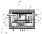
- FIG. 11 is a cross-sectional structural schematic diagram showing a power module according to Embodiment 5;
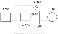
- FIG. 12 is a block diagram showing the configuration of a power conversion system to which a power conversion device according to Embodiment 6 is applied;
- FIG. 1 is a schematic plan view showing a power module according to Embodiment 1.
- FIG. FIG. 2 is a cross-sectional schematic diagram showing the power module according to Embodiment 1.
- FIG. 3 is a cross-sectional schematic diagram showing the power module according to Embodiment 1.
- FIG. 4 is a cross-sectional schematic diagram showing the power module according to Embodiment 1.
- FIG. 5 is a cross-sectional schematic diagram showing the power module according to Embodiment 1.
- FIG. FIG. 6 is a cross-sectional schematic diagram showing another power module according to Embodiment 1.
- FIG. FIG. 2 is a schematic cross-sectional view taken along the dashed-dotted line AA in FIG. FIG.
- FIG. 3 is a schematic cross-sectional view taken along dashed-dotted line BB in FIG.
- FIG. 4 is a schematic cross-sectional view taken along dashed-dotted line CC in FIG.
- FIG. 5 is a schematic cross-sectional view taken along the dashed-dotted line AA in FIG. 1 when the cooling unit 1 is attached to the power module 100.
- FIG. 6 is a schematic cross-sectional view taken along dashed-dotted line AA in FIG.
- a power module 100 includes a lid portion 2, a pressure portion 2a, a frame 3, a power semiconductor element 5 as a semiconductor element, solder 6 as a bonding material (bonding portion), and an insulating substrate 7. , a heat spreader 8 that is a heat diffusion part, wiring 9 that is a connection wiring part, bolts 4 and 11 that are fastening members, and external connection terminals 10 .
- the metal layer 7c on the lower surface side of the insulating substrate 7 is joined to the upper surface of the heat spreader 8 via the solder 6.
- the back surface of the power semiconductor element 5 is joined to the metal layer 7 a on the upper surface side of the insulating substrate 7 via solder 6 .
- Wiring 9 is joined to the surface of power semiconductor element 5 and metal layer 7 b on the upper surface side of insulating substrate 7 via solder 6 .
- External connection terminals 10 are joined to the upper surface of the metal layer 7a and the upper surface of the metal layer 7b on the upper surface side of the insulating substrate 7, respectively.
- a frame 3 surrounding the insulating substrate 7 is arranged in the outer peripheral region of the upper surface of the heat spreader 8 .
- the bottom surface of the frame 3 is joined to the top surface of the heat spreader 8 .
- a lid portion 2 is arranged on the upper surface of the frame body 3 . Between the lower surface of the lid portion 2 and the upper surface of the wiring 9, a pressurizing portion 2a for pressurizing the solder 6 that joins the power semiconductor element 5 and the metal layer 7a is arranged.
- a sealing member 20 is arranged (filled) in the interior surrounded by the heat spreader 8 and the frame 3 .
- FIG. 1 is a schematic plan view of the power module 100 viewed from the upper surface side through the cover 2 .
- a transparent member is indicated by a dotted line.
- the outermost solid line is the outer edge of the lid 2 and the outer edge (outer wall) of the frame 3.
- An inner edge (inner wall) of the frame 3 is arranged inside the outer edge of the frame 3 .
- the outer edge of the heat spreader 8 is arranged at the same position as the outer edge of the lid portion 2 (the outer edge of the frame 3).
- the outer edge of the insulating layer 7 d of the insulating substrate 7 is arranged inside the inner edge of the frame 3 .
- Metal layers 7 a and 7 b on the upper surface side of the insulating substrate 7 are arranged inside the outer edge of the insulating layer 7 d of the insulating substrate 7 .
- the power semiconductor element 5 and the external connection terminals 10 are arranged inside the outer edge of the upper surface of the metal layer 7a on the upper surface side of the insulating substrate 7 .
- Wires 9 are arranged inside the outer edges of the upper surface of the power semiconductor element 5 and the metal layer 7b on the upper surface side of the insulating substrate 7, respectively.
- the wiring 9 is located inside the outer edge of the metal layer 7a and the metal layer 7b on the upper surface side of the insulating substrate 7, straddling the gap (spaced portion) between the outer edges of the metal layer 7a and the metal layer 7b facing each other. , the metal layer 7a and the metal layer 7b.
- a pressure member 2 a is arranged on the wiring 9 above the power semiconductor element 5 inside the outer edge of the power semiconductor element 5 .
- Fastening holes 2 b for arranging bolts 4 and 11 are arranged between the outer edge and the inner edge of the frame 3 .
- FIG. 2 is a schematic cross-sectional view of a portion corresponding to the fastening hole 2b for fastening with the cooling section 1 of the power module 100.
- the metal layer 7c on the lower surface side of the insulating substrate 7 is joined to the upper surface of the heat spreader 8 via the solder 6.
- the back surface of the power semiconductor element 5 is joined to the metal layer 7 a on the upper surface side of the insulating substrate 7 via solder 6 .
- Wiring 9 is joined to the surface of power semiconductor element 5 and the upper surface of metal layer 7 b on the upper surface side of insulating substrate 7 via solder 6 .
- External connection terminals 10 are joined to the upper surface of the metal layer 7a and the upper surface of the metal layer 7b on the upper surface side of the insulating substrate 7, respectively.
- a frame 3 surrounding the insulating substrate 7 is arranged in the outer peripheral region of the upper surface of the heat spreader 8 .
- the lower surface of the frame 3 is joined to the upper surface of the heat spreader 8
- the lid portion 2 is arranged on the upper surface of the frame 3 .
- a pressurizing portion 2a for pressurizing the solder 6 that joins the power semiconductor element 5 and the metal layer 7a is arranged.
- a sealing member 20 is arranged inside the frame 3 .
- Fastening holes 2 b for inserting bolts 4 are arranged at corresponding portions of the frame 3 , the lid portion 2 and the heat spreader 8 .
- the fastening hole 2 b is formed through the lid portion 2 , the frame 3 and the heat spreader 8 .
- the external connection terminal 10 protrudes outside the lid portion 2 through a predetermined position of the lid portion 2 .
- FIG. 3 is a schematic cross-sectional view of a portion corresponding to the fastening hole 2b for fastening the power module 100 to the heat spreader 8.
- FIG. 3 differs from FIG. 2 in the shape of the fastening hole 2b into which the fastening member 4 is inserted.
- the bottom of the fastening hole 2 b does not penetrate the heat spreader 8 and stops inside the heat spreader 8 .
- FIG. 4 is a schematic cross-sectional view of a portion corresponding to a region where the power semiconductor element 5 of the power module 100 is pressurized by the pressurizing portion 2a.
- the back surface of the power semiconductor element 5 is bonded to the upper surface of the metal layer 7a on the upper surface side of the insulating substrate 7 via solder 6 as a bonding material.
- An electrode (not shown) is formed on the surface of the power semiconductor element 5 , and the lower surface of the wiring 9 and the electrode of the power semiconductor element 5 are joined via solder 6 .
- a pressurizing portion 2 a is arranged above the power semiconductor element 5 and on the upper surface of the wiring 9 .
- the pressurizing portion 2a is arranged so that the lower surface is in contact with the upper surface of the wiring 9 and the upper surface is in contact with the lower surface of the lid portion 2 .
- the lid portion 2 can be fastened to the heat spreader 8 using the bolts 11.
- the solder 6 that joins the power semiconductor element 5 to the metal layer 7a on the upper surface side of the insulating substrate 7 can be pressurized.
- FIG. 5 is a schematic cross-sectional view of the cooling unit 1 attached to the power module 100.
- the upper surface of cooling unit 1 is arranged so as to be in contact with the lower surface of heat spreader 8 .
- Cooling unit 1 is fastened to power module 100 with bolts 4 . If the pressurizing force applied to the solder 6 is insufficient when the bolts 11 are used for fastening, the pressurizing force can be increased when the bolts 4 are used for fastening.
- the heat spreader 8 is a plate-like bottom portion (bottom plate) of the power module 100 that includes the insulating substrate 7 and the like.
- the heat spreader 8 extends in the first direction and the second direction.
- the heat spreader 8 functions as a heat diffusion member for dissipating heat generated inside the power module 100 to the outside of the power module 100 .
- the upper surface of the heat spreader 8 is bonded to the lower surface of the metal layer 7c on the lower surface side of the insulating substrate 7 via (using) solder 6 as a bonding material.
- a copper alloy, an aluminum alloy, or the like can be used as a material for the heat spreader 8.
- the lower surface of the sealing member 20 is in contact with the outside of the bonding area with the solder 6 on the upper surface of the heat spreader 8 .
- a metal with good thermal conductivity such as copper (Cu) or aluminum (Al), or a material such as a graphite material can be used.
- the insulating substrate 7 extends in the first direction and the second direction.
- the insulating substrate 7 is a plate-like member.
- the insulating substrate 7 has an upper surface layer, an intermediate layer and a lower surface layer.
- a metal layer 7 c on the lower surface side of the insulating substrate 7 faces the upper surface of the heat spreader 8 .
- the insulating substrate 7 has an insulating layer 7d as an intermediate layer, a metal layer 7a as an upper surface layer on the upper surface side of the insulating layer 7d, and a metal layer 7c as a lower surface layer on the lower surface side of the insulating layer 7d.
- a metal layer 7 c on the lower surface side of the insulating layer 7 d is joined to the upper surface of the heat spreader 8 with solder 6 .
- the insulating substrate 7 is plate-shaped, and when the plate-shaped insulating substrate 7 is viewed from the plane (upper surface) direction, the size of the metal layer 7a on the upper surface side of the insulating layer 7d is smaller than the size of the insulating layer 7d. It's becoming The size of the metal layer 7c on the lower surface side of the insulating layer 7d is smaller than the size of the insulating layer 7d. The end of insulating layer 7d protrudes outward beyond the ends of metal layer 7a on the upper surface side of insulating layer 7d and metal layer 7c on the lower surface side of insulating layer 7d.
- the insulating layer 7d is sandwiched between the metal layer 7a on the upper surface side of the insulating layer 7d and the metal layer 7c on the lower surface side of the insulating layer 7d and the heat spreader 8, thereby suppressing creeping discharge (securing a creeping distance). It is for
- the metal layer 7a on the upper surface side of the insulating layer 7d may be divided into a plurality of parts depending on the purpose to form a circuit pattern.
- the power semiconductor element 5 and the external connection terminals 10 are arranged on the metal layer 7a.
- a wire and an external connection terminal 10 are arranged on the metal layer 7b.
- a ceramic substrate such as aluminum oxide ( Al2O3 ), aluminum nitride ( AlN) or silicon nitride ( Si3N4 ) can be used.
- a metal layer (circuit pattern plate) 7a and a metal layer (relay plate) 7b are joined to the upper surface of the insulating layer 7d by brazing or direct joining.
- a metal layer (radiating plate) 7c is joined to the lower surface of the insulating layer 7d by using a method such as brazing or direct joining.
- a method such as brazing or direct joining.
- any good electrical conductor such as Cu or Al can be used.
- a material having a two-layer structure obtained by laminating Cu and Al may be used as the metal layer 7a, the metal layer 7b, and the metal layer 7c, respectively.
- Al serves as a stress relaxation layer for bonding Cu and the insulating substrate 7, so the side closer to the insulating layer 7d is the Al layer and the far side is the Cu layer.
- the upper surface side of the insulating substrate 7 is synonymous with the upper surface side of the insulating layer 7d
- the lower surface side of the insulating substrate 7 is synonymous with the lower surface side of the insulating layer 7d.
- the power semiconductor element 5 has a structure in which electrodes (not shown) are arranged on the surface of the power semiconductor element 5 .
- the power semiconductor element 5 is bonded to the upper surface of the metal layer 7a on the upper surface side of the insulating substrate 7 via solder 6 as a bonding portion.
- silicon Si: Silicon
- silicon carbide SiC: Silicon Carbide
- gallium nitride GaN: Gallium Nitride
- the power semiconductor element 5 is a MOSFET (Metal Oxide Semiconductor Field Effect Transistor), IGBT (Insulated Gate Bipolar Transistor), FWD (Free Wheel Diode), and RC-IGBT (Reverse Conducting Power IGBT) device.
- MOSFET Metal Oxide Semiconductor Field Effect Transistor
- IGBT Insulated Gate Bipolar Transistor
- FWD Free Wheel Diode
- RC-IGBT Reverse Conducting Power IGBT
- the wiring 9 is a plate-like metal member. One end of the wiring 9 is electrically connected to the electrode of the power semiconductor element 5 on the metal layer 7 a on the upper surface side of the insulating substrate 7 . The wiring 9 has the other end electrically connected to a predetermined position of the metal layer 7b. The wiring 9 is connected to the electrodes of the power semiconductor element 5 via the solder 6 . Further, the wiring 9 is connected to the metal layer 7b through the solder 6. As shown in FIG. The wiring 9 is made of a good conductor metal with sufficient rigidity, for example, a copper plate can be used.
- the wiring 9 when Al is used as the material of the wiring 9, it can be used if the surface of the Al is configured so that it can be soldered by nickel (Ni) plating or the like. Furthermore, although both ends of the wiring 9 are joined by solder 6, they may be joined by ultrasonic joining or the like. Moreover, the wiring 9 can use a Cu ribbon material, an Al ribbon material, or the like, which can provide sufficient rigidity. The wiring 9 may be bonded to the power semiconductor element 5 or the metal layer 7b using ultrasonic bonding.
- the external connection terminal 10 is joined to a predetermined position on the metal layer 7a and a predetermined position on the metal layer 7b using ultrasonic bonding.
- the other end of the external connection terminal 10 is taken out (protrudes) from a through hole provided in the side surface of the frame 3 .
- the external connection terminal 10 can also have a structure in which an insulation bush (not shown) is inserted into the side surface of the frame 3 to ensure a long creepage insulation distance.
- the external connection terminals 10 protrude to the outside of the power module 100 from through holes provided in the side surface of the frame 3 in FIG. 2 .
- a through hole or a notch may be provided in the side surface of the frame 3 as shown in FIG.
- the external connection terminal 10 is joined to the metal layer 7a or the metal layer 7b using ultrasonic bonding, but may be joined using solder.
- the frame 3 and the lid 2 a highly rigid resin such as PPS resin (Poly Phenylene Sulfide Resin) can be used.
- the frame 3 and the lid portion 2 may be made of highly rigid metal such as Cu, Al, and stainless steel in order to increase rigidity.
- the lid portion 2 has a pressurizing portion 2a protruding toward the inside of the power module 100 of the lid portion 2 (upper surface side of the wiring 9).
- the coating amount of the resin material which is the material of the pressurizing portion 2a
- an insulator such as ceramic may be used.
- the frame 3 is a frame that surrounds the insulating substrate 7 .
- the pressurizing portion 2a may be formed integrally with the lid portion 2 or may be formed separately from the lid portion 2 .
- the shape of the lower surface side of the lid portion 2 may be the same plane as long as it is in contact with the upper surface of the frame body 3 . Further, the shape of the lower surface of the lid portion 2 may be such that it protrudes toward the heat spreader 8 inside the inner edge of the frame 3 . With such a shape, the lower surface of the lid portion 2 can be in contact with the upper surface of the pressurizing portion 2a, so that the solder 6 that joins the power semiconductor element 5 can be reliably pressurized.
- the fastening holes 2b provided in the lid portion 2 and the frame 3 may be appropriately formed according to the size (thickness) of the bolts 4 and 11 used for fastening.
- the size is not particularly limited as long as the lid portion 2, the frame body 3, the heat spreader 8 and the cooling portion 1 can be fastened together and the required pressure can be applied to the pressure portion 2a.
- the bolts 4 pass through the heat spreader 8 and fasten the lid part 2 and the frame body 3 to the cooling part 1 .
- the bolts 11 fasten the lid portion 2 and the frame body 3 to the heat spreader 8 .
- the bolts 4 and 11 are passed through (inserted into) fastening holes 2b provided in the lid portion 2 and the frame body 3 to fasten the lid portion 2 and the frame body 3 to the heat spreader 8 or the cooling portion 1 with an appropriate fastening force. .
- heat conductive grease or a graphite sheet (not shown) is interposed between the heat spreader 8 and the cooling unit 1 to reduce thermal resistance.
- the head of the bolt 4 is embedded in the lid portion 2. However, even if the head portion is protruded outside the lid portion 2 as shown in FIG. good. Common bolts can be used as the bolts 4 and 11 .
- the bonding material 6 bonds the heat spreader 8 to the insulating substrate 7 , the insulating substrate 7 to the power semiconductor element 5 , and the insulating substrate 7 to the wiring 9 .
- Tin (Sn)-based solder can be used as the solder 6 which is a joining material.
- antimony (Sb), silver (Ag), Cu, and the like are added to such Sn-based solders in order to provide stress relaxation properties, heat resistance, and fatigue resistance strength, and the composition can be arbitrarily selected.
- the solder 6 joins the members to be joined by reflowing together with the members to be joined.
- solder As a bonding material for die bonding, general solder was used as an example, but in addition to solder, TLP bonding (Transient Liquid Phase), nanoparticles such as Ag or Cu are used. There is also a sintered type joining material, which can be applied to the present disclosure, but a solder material is most suitable from the viewpoint of cost reduction and process stability.
- the sealing member 20 is filled inside the frame 3 .
- the sealing member 20 seals the insulating substrate 7 and the power semiconductor element 5 .
- epoxy resin containing filler such as silicone gel or silica can be used.
- silicone gel is used as the material of the sealing member 20, the pressurizing effect of the pressurizing portion 2a is sufficiently exhibited.
- the upper surface of the sealing member 20 can be filled inside the frame 3 within a range from the same height as the upper surface of the wiring 9 (FIG. 6) to the height contacting the lower surface of the lid 2 (FIG. 5).
- the upper surface of the sealing member 20 is higher than the upper surface of the wiring 9, by disposing a dummy member in advance in the region where the pressure member 2a is arranged and then filling the sealing member 20, It is possible to secure an arrangement area for the pressure part 2a. In this case, the wiring 9 is sealed with the sealing member 20 except for the arrangement position of the pressure member 2a. Moreover, when the upper surface of the sealing member 20 is at the same height as the upper surfaces of the wirings 9, it is desirable to secure a distance from the external connection terminals 10. FIG. If it is difficult to secure the distance between the wiring 9 and the external connection terminal 10 , the height of the upper surface of the sealing member 20 should be set to a height that covers the upper surface of the wiring 9 .
- the thickness of the sealing member 20 that covers the upper surface of the wiring 9 should be at least 100 ⁇ m.
- the thickness of the sealing member 20 covering the upper surface of the wiring 9 can be appropriately selected within a range of 100 ⁇ m or more according to the voltage of the power module used.
- the cooling part 1 is a flat metal member. Cu, Al, or the like can be used as the material of the cooling part 1 .
- the cooling unit 1 shown in FIG. 5 is displayed by simulating a top plate of a water jacket or a heat sink, and the configuration of the cooling unit 1 other than the top plate may be of any configuration.
- a heat sink is used as the cooling unit 1, not only air cooling but also water cooling or liquid cooling may be used as the cooling method.
- the difference in linear expansion coefficient between the power semiconductor element 5 and the insulating substrate 7 is small, preferably 5 ppm/K.
- the following countermeasures are taken to suppress horizontal cracking caused by cracks extending horizontally inside the solder 6 .
- the solder 6 is pressurized through the wiring 9 by the pressurizing portion 2a on the lower surface side of the lid portion 2 in order to suppress the generation of cracks due to the equibiaxial tensile-compressive deformation.
- the deformation is no longer equal biaxial tension-compression deformation, so longitudinal cracking of the solder 6 can be suppressed.
- the power module 100 is constructed using the pressurizing portion 2a in this way, the occurrence of longitudinal cracks in the solder 6 that joins the power semiconductor element 5 to the metal layer 7a on the upper surface side of the insulating substrate 7 can be suppressed. Since the heat dissipation of the power semiconductor element 5 during operation is not interrupted, the reliability of the power module 100 can be improved. Moreover, the life of the power module 100 can be extended.
- the power module can be miniaturized.
- FIG. 7 is a cross-sectional schematic diagram showing another power module according to Embodiment 1.
- FIG. FIG. 7 is a cross-sectional view of the heat spreader 8 attached to the cooling unit 1 with bolts 4.
- the heat spreader 8 does not extend to the outer edge of the frame 3, and the outer surface of the heat spreader 8 and the inner surface of the frame 3 are in contact with each other. 3c is formed.
- a corner portion 3 c of the frame 3 is a fitting portion for fitting the frame 3 and the heat spreader 8 .
- FIG 8 to 13 are cross-sectional structural schematic diagrams showing the manufacturing process of the power module according to the first embodiment.
- the main manufacturing processes of the first embodiment are roughly divided into five processes.
- the power semiconductor element 5 and the like are bonded onto the insulating substrate 7 (mounting step on the insulating substrate).
- the insulating substrate 7 to which the power semiconductor element 5 and the like are joined and the frame 3 are joined on the heat spreader 8 (mounting step on the heat spreader).
- the sealing member 20 is filled in the region surrounded by the heat spreader 8 and the frame 3 (frame resin filling step).
- the lid portion 2 is placed on the frame body 3 filled with the sealing member 20 (lid fastening step).
- the heat spreader 8 and the cooling unit 1 are fastened together (cooling unit fastening step).
- the power semiconductor element 5, the wiring 9, and the external connection terminal 10 are joined (arranged) at predetermined positions on the metal layers 7a and 7b on the upper surface side of the insulating substrate 7 (insulating substrate 7). mounting process).
- Solder 6 is used as a bonding material for bonding the power semiconductor element 5 and the wiring 9 .
- the external connection terminals 10 can be joined to the metal layers 7a and 7b on the upper surface side of the insulating substrate 7 by soldering 6 or ultrasonic joining.
- the insulating substrate 7 on which the power semiconductor elements 5 and the like are arranged is bonded (arranged) on the upper surface of the heat spreader 8 .
- the frame 3 is arranged surrounding the insulating substrate 7 in the outer peripheral region of the upper surface of the heat spreader 8 (mounting process to the heat spreader). Solder is usually used for bonding the insulating substrate 7 .
- An adhesive is usually used for bonding (bonding) the frame 3 .
- the insulating substrate 7 is placed, and the area surrounded by the frame 3 and the heat spreader 8 is filled with the sealing member 20 .
- the height of the upper surface of the sealing member 20 from the upper surface of the heat spreader 8 can be in the range from the upper surface of the wiring 9 to the upper surface of the frame 3 , in other words, the height of contact with the lower surface of the lid portion 2 .
- the sealing member 20 may be filled after disposing the pressurizing portion 2a at a predetermined position on the upper surface of the wiring 9 in advance.
- the sealing member 20 is filled so as to fill the space.
- the height of the sealing member 20 can be appropriately selected within a range from the upper surface of the wiring 9 to the lower surface of the lid portion 2 as necessary.
- FIG. 11 is a display in which the cross section AA (FIG.
- FIG. 12 shows a cross-sectional shape of a fastening hole 2b into which a bolt 4 for fastening with the cooling part 1 is inserted.
- the connection between the heat spreader 8 and the cooling unit 1, which connects the lower surface of the heat spreader 8 and the upper surface of the cooling unit 1, is performed using bolts 4 (cooling unit fastening process).
- bolts 4 cooling unit fastening process
- pressure can be applied in the direction indicated by the arrow (the direction from the pressurizing portion 2a toward the insulating substrate 7 in the Z direction).
- a thermally conductive material such as a thermal interface material (TIM) or a graphite sheet may be sandwiched between the heat spreader 8 and the cooling unit 1 to efficiently dissipate heat.
- the power module 100 including the cooling section 1 can be manufactured.
- the pressurizing portion 2a is provided between the lower surface of the lid portion 2 and the upper surface of the wiring 9, the power semiconductor element 5 is placed on the metal layer 7a on the upper surface side of the insulating substrate 7. It is possible to pressurize the solder 6 that is joined to the solder 6 and suppress the occurrence of longitudinal cracks in the solder 6 . As a result, reliability of the power module can be improved. Also, the life of the power module can be extended.
- the pressurizing portion 2a is provided between the lower surface of the lid portion 2 and the upper surface of the wiring 9, the power module can be easily manufactured.
- the pressurizing portion 2a is provided between the lower surface of the lid portion 2 and the upper surface of the wiring 9, it is possible to suppress the occurrence of longitudinal cracks in the solder 6, thereby suppressing an increase in the resistance of the power module.
- Embodiment 2 In the second embodiment, the external connection terminals 10 used in the first embodiment are exposed (protruded) from the side surface of the frame 3 to the outside of the power module, and the pressure member 2a is used as the pressure member 14.
- the heat spreader 8 is arranged so as to be in contact with not only the wiring 9 but also the external connection terminals 10 and that the heat spreader 8 has a heat spreader upper surface portion 12 and a heat spreader side surface portion 13 .
- the pressure member 14 is arranged so as to be in contact with the upper surfaces of the wirings 9 and the external connection terminals 10.
- the solder 6 that joins the power semiconductor element 5 and the metal layer 7a on the upper surface side of the insulating substrate 7 can be pressurized, and vertical cracking of the solder 6 can be suppressed.
- the heat spreader upper surface portion 12 and the heat spreader side surface portion 13 which are thermally connected to the heat spreader 8 are provided so as to be in contact with the upper surface of the external connection terminal 10 and the upper surface of the wiring 9 via the pressurizing portion 14, the power semiconductor Heat generated from the device 5 or the external connection terminals 10 can be dissipated to the heat spreader 8 and the cooling unit 1 via the heat spreader upper surface portion 12 and the heat spreader side surface portion 13. Heat can be efficiently dissipated and the cooling capacity can be improved.
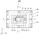
- FIG. 14 is a schematic plan view showing the power module according to Embodiment 2.
- FIG. 15 is a cross-sectional schematic diagram showing a power module according to Embodiment 2.
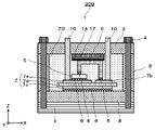
- FIG. 16 is a cross-sectional schematic diagram showing a power module according to Embodiment 2.
- FIG. 15 is a schematic cross-sectional view taken along dashed-dotted line DD in FIG.
- FIG. 16 is a schematic cross-sectional view taken along dashed-dotted line EE in FIG.
- the power module 200 includes a lid portion 2, a pressurizing portion 14, a frame 3, a power semiconductor element 5, a solder 6 as a bonding material, an insulating substrate 7, and a heat spreader 8 as a heat diffusion portion.
- the heat spreader upper surface portion 12 that is the upper surface portion of the heat spreader
- the heat spreader side surface portion 13 that is the side surface portion of the heat spreader
- the wiring 9 that is the connection wiring portion
- the bolts 4 and 11 that are fastening members
- the external connection a terminal 10 the external connection a terminal 10
- the metal layer 7c on the lower surface side of the insulating substrate 7 is joined to the upper surface of the heat spreader 8 via solder.
- the back surface of the power semiconductor element 5 is joined to the metal layer 7a on the upper surface side of the insulating substrate 7 via solder.
- Wiring 9 is joined to the surface of power semiconductor element 5 and metal layer 7b on the upper surface side of insulating substrate 7 via solder.
- External connection terminals 10 are joined to the upper surface of the metal layer 7a and the upper surface of the metal layer 7b on the upper surface side of the insulating substrate 7, respectively.
- a frame 3 surrounding the insulating substrate 7 is arranged in the outer peripheral region of the upper surface of the heat spreader 8 .
- the bottom surface of the frame 3 is joined to the top surface of the heat spreader 8 .
- a lid portion 2 is arranged on the upper surface of the frame body 3 .
- the lower surface of the lid portion 2 is in contact with the upper surface of the heat spreader upper surface portion.
- a pressure member 14 for applying pressure to the solder 6 that joins the power semiconductor element 5 and the metal layer 7a is arranged between the lower surface of the upper surface of the heat spreader and the upper surface of the wiring 9, a pressure member 14 for applying pressure to the solder 6 that joins the power semiconductor element 5 and the metal layer 7a is arranged.
- a sealing member 20 is arranged (filled) in the interior surrounded by the heat spreader 8 and the frame 3 .
- FIG. 14 is a schematic plan view of the power module 200 viewed from the upper surface side through the cover 2.
- FIG. A transparent member is indicated by a dotted line.
- the outermost solid line is the outer edge of the lid portion 2 and the outer edge (outer wall) of the frame 3 .
- An inner edge (inner wall) of the frame 3 is arranged inside the outer edge of the frame 3 .
- the outer edge of the heat spreader 8 is arranged at the same position as the outer edge of the lid portion 2 (outer edge of the frame).
- the outer edge of the insulating layer 7 d of the insulating substrate 7 is arranged inside the inner edge of the frame 3 .
- Metal layers 7 a and 7 b on the upper surface side of the insulating substrate 7 are arranged inside the outer edge of the insulating layer 7 d of the insulating substrate 7 .
- the power semiconductor element 5 and the external connection terminals 10 are arranged inside the outer edge of the upper surface of the metal layer 7 a on the upper surface side of the insulating substrate 7 .
- Wires 9 are arranged inside the outer edges of the upper surface of the power semiconductor element 5 and the metal layer 7b on the upper surface side of the insulating substrate 7, respectively.
- the wiring 9 is located inside the outer edge of the metal layer 7a and the metal layer 7b on the upper surface side of the insulating substrate 7, straddling the gap (spaced portion) between the outer edges of the metal layer 7a and the metal layer 7b facing each other. , the metal layer 7a and the metal layer 7b.
- a pressurizing portion 14 is arranged inside the inner edge of the frame 3 of the external connection terminal 10 protruding outside from the opposite side and on the upper surface of the wiring 9 .
- Fastening holes 2 b for arranging bolts 4 and 11 are arranged between the outer edge and the inner edge of the frame 3 .
- the heat spreader upper surface portion 12 is arranged so as to cover the entire inner edge of the frame 3 .
- the heat spreader side portions 13 are arranged on both sides along opposite sides of the frame 3 in the first direction.
- FIG. 15 is a schematic cross-sectional view of a portion corresponding to the external connection terminal 10 of the power module 200.
- the metal layer 7c on the lower surface side of the insulating substrate 7 is joined to the upper surface of the heat spreader 8 via the solder 6.
- the back surface of the power semiconductor element 5 is joined to the metal layer 7 a on the upper surface side of the insulating substrate 7 via solder 6 .
- Wiring 9 is joined to the surface of power semiconductor element 5 and metal layer 7 b on the upper surface side of insulating substrate 7 via solder 6 .
- External connection terminals 10 are joined to the upper surface of the metal layer 7a and the upper surface of the metal layer 7b on the upper surface side of the insulating substrate 7, respectively.
- the external connection terminals 10 protrude to the outside of the power module 200 from the side surfaces of the frame 3 facing each other.
- a region of the frame 3 where the external connection terminal 10 protrudes to the outside is provided with a hole or a notch through which the external connection terminal 10 protrudes to the outside. If the frame 3 is provided with a notch, the corresponding region of the lid 2 may have a shape that fits the notch of the frame 3 while holding the external connection terminal 10 therebetween.
- a frame 3 surrounding the insulating substrate 7 is arranged in the outer peripheral region of the upper surface of the heat spreader 8 .
- the lower surface of the frame 3 is joined to the upper surface of the heat spreader 8
- the lower surface of the lid portion 2 is arranged on the upper surface of the frame 3 .
- a pressure applying portion 14 for applying pressure to the solder 6 that joins the power semiconductor element 5 and the metal layer 7a is arranged via the heat spreader upper surface portion 12.
- a sealing member 20 is arranged inside the frame 3 .
- Fastening holes 2 b for inserting bolts 4 are arranged in the lid portion 2 corresponding to the frame 3 and the heat spreader 8 .
- the fastening hole 2 b is formed through the lid portion 2 , the frame 3 and the heat spreader 8 .
- the external connection terminal 10 protrudes outside the lid portion 2 through a predetermined position of the lid portion 2 .
- the pressurizing portion 14 and the heat spreader upper surface portion 12 extend in the first direction.
- FIG. 16 is a schematic cross-sectional view of a portion of the power module 200 corresponding to the area where the power semiconductor element 5 is pressurized by the pressurizing portion 14.
- the back surface of the power semiconductor element 5 is bonded to the upper surface of the metal layer 7a on the upper surface side of the insulating substrate 7 via solder 6 as a bonding material.
- An electrode (not shown) is formed on the surface of the power semiconductor element 5 , and the lower surface of the wiring 9 and the electrode of the power semiconductor element 5 are joined via solder 6 .
- a pressure member 14 is arranged above the power semiconductor element 5 and on the upper surface of the wiring 9 .
- the pressurizing part 14 is arranged so that its lower surface is in contact with the upper surface of the wiring 9 and its upper surface is in contact with the lower surface of the heat spreader upper surface part 12 .
- the lid portion 2 is fastened to the heat spreader 8 using the bolts 11.
- the solder 6 that joins the power semiconductor element 5 to the metal layer 7a on the upper surface side of the insulating substrate 7 can be pressurized.
- the heat spreader 8 has a heat spreader side surface portion 13 and a heat spreader top surface portion 12 surrounding the insulating substrate 7 inside the inner wall of the frame 3 .
- the upper surface of the heat spreader upper surface portion 12 is in contact with the lower surface of the lid portion 2 .
- the lower surface of the heat spreader upper surface portion 12 is in contact with the upper surface of the pressurizing portion 14 .
- the heat spreader upper surface portion 12 is supported by the heat spreader side surface portion 13 .
- the heat spreader side portions 13 face each other in the second direction of the frame 3 and are arranged along the sides of the frame 3 in the first direction.
- the insulating substrate 7 is arranged at a position sandwiched by the heat spreader side portions 13 arranged to face each other.
- the heat spreader upper surface portion 12 is supported by two heat spreader side surface portions 13 arranged at opposite positions.
- the heat spreader side surface portion 13 may be divided into a plurality of portions so that the heat spreader upper surface portion 12 can be supported on both
- the external connection terminal 10 may secure a long creepage insulation distance by inserting an insulation bush (not shown) into a projecting region projecting from the side surface of the frame 3 to the outside of the power module 200 .
- the pressurizing part 14 is in contact not only with the upper surfaces of the wirings 9 but also with the upper surfaces of the external connection terminals 10 .
- the contact area between the upper surface of the wiring 9 and the upper surface of the external connection terminal 10 although not shown, thermal grease, graphite sheet, or the like is applied to the upper surface of the wiring 9 and the external connection in order to improve contact and heat conduction. It may be inserted between the upper surface of the terminal 10 and the lower surface of the pressure member 14 .
- the heat spreader 8 has a heat spreader upper surface portion 12 and a heat spreader side surface portion 13 .
- the heat spreader upper surface portion 12 is supported by a plurality of heat spreader side surface portions 13 .
- a heat spreader upper surface portion 12 in contact with the upper surface side of the power semiconductor element 5 is thermally connected to the heat spreader 8 or the cooling portion 1 via a heat spreader side surface portion 13 . Therefore, the heat generated in the power semiconductor element 5 can be radiated not only from the metal layer 7c side on the lower surface side of the insulating substrate 7, but also from the heat spreader upper surface portion 12 side on the upper surface side of the power semiconductor element 5. Therefore, the heat generated by the power semiconductor element 5 can be cooled more effectively.
- a metal with good thermal conductivity such as Cu or Al, a graphite material, or the like can be used.
- the pressure member 14 contacts the wiring 9 and the external connection terminal 10 , it is made of an insulator similar to the insulating substrate 7 .
- the pressure member 14 can be made of a ceramic substrate such as Si 3 N 4 (silicon nitride), AlN (aluminum nitride), Al 2 O 3 (alumina), resin material, or the like.
- the heat spreader upper surface portion 12 is connected to the cooling portion 1 or the heat spreader 8 through the heat spreader side surface portion 13, so that the power semiconductor element 5 is connected through the wiring 9 or the external connection terminal 10. heat can be dissipated (cooled), and not only can the solder 6 be pressurized, but also the heat resistance can be further lowered, so the life of the power module 200 can be further extended.
- the pressurizing portion 14 is arranged so as to be in contact with the entire upper surface of the wiring 9, the entire upper surface of the wiring 9 can be pressurized. Sufficient pressure can be generated against 6.
- the external connection terminals 10 are arranged so as to protrude from the side surfaces of the frame 3 to the outside.
- the heat spreader upper surface portion 12 is supported by the respective upper surfaces of the heat spreader side surface portions 13 arranged to face each other, and is arranged in contact with the upper surface of the pressure member 14 and the lower surface of the lid portion 2 . .
- the power module 200 including the cooling section 1 can be manufactured.
- the pressure member 14 is provided between the lower surface of the heat spreader upper surface portion 12 and the upper surface of the wiring 9 and the upper surface of the external connection terminal 10, so that the power semiconductor element 5 is placed on the insulating substrate.
- the solder 6 bonded to the metal layer 7a on the upper surface side of 7 can be pressurized, and the occurrence of vertical cracks in the solder 6 can be suppressed. As a result, reliability of the power module can be improved. Also, the life of the power module can be extended.
- the heat spreader upper surface portion 12 is provided between the lower surface of the lid portion 2 and the upper surface of the pressurizing portion 14 and is connected to the heat spreader 8 via the heat spreader side surface portion 13, power is also supplied from the upper surface side of the power semiconductor element 5. Heat generated in the semiconductor element 5 or the external connection terminal 10 can be dissipated, and the heat dissipation of the power module can be improved.
- the pressurizing part 14 is arranged so as to be in contact with the entire upper surface of the wiring 9, the entire upper surface of the wiring 9 can be pressurized. Sufficient pressure can be generated against 6.
- the pressing portion 14 used in the first embodiment is arranged so as to be in contact with the entire upper surface of the wiring 9, and the heat spreader 8 has a heat spreader upper surface portion 12 and a heat spreader side surface portion 13. different. Since the pressurizing part 14 is arranged so as to be in contact with the entire upper surface of the wiring 9 in this manner, the solder 6 that joins the power semiconductor element 5 and the metal layer 7a on the upper surface side of the insulating substrate 7 can be pressurized. Vertical cracks in the solder 6 can be suppressed.
- the heat spreader upper surface portion 12 and the heat spreader side surface portion 13 connected to the heat spreader 8 are provided so as to be in contact with the upper surface of the external connection terminal 10 and the upper surface of the wiring 9 via the pressurizing portion 14, the power semiconductor element 5 or The heat generated from the external connection terminal 10 can be dissipated to the heat spreader 8 and the cooling unit 1 via the heat spreader upper surface portion 12 and the heat spreader side surface portion 13, and the heat generated in the power semiconductor element 5 and the external connection terminal 10 can be efficiently dissipated. It can dissipate heat and improve cooling capacity.
- FIG. 17 is a schematic plan view showing a power module according to Embodiment 3.
- FIG. 18 is a cross-sectional schematic diagram showing a power module according to Embodiment 3.
- FIG. 19 is a cross-sectional schematic diagram showing a power module according to Embodiment 3.
- FIG. 18 is a schematic cross-sectional view taken along dashed-dotted line FF in FIG.
- FIG. 19 is a schematic cross-sectional view along the dashed-dotted line GG in FIG.
- a power module 300 includes a lid portion 2, a pressure portion 14, a frame 3, a power semiconductor element 5, a solder 6 as a bonding material, an insulating substrate 7, and a heat spreader 8 as a heat diffusion portion.
- the heat spreader upper surface portion 12 that is the upper surface portion of the heat spreader
- the heat spreader side surface portion 13 that is the side surface portion of the heat spreader
- the wiring 9 that is the connection wiring portion
- the bolts 4 and 11 that are fastening members
- the external connection a terminal 10 the external connection a terminal 10
- the metal layer 7c on the lower surface side of the insulating substrate 7 is joined to the upper surface of the heat spreader 8 via solder.
- the back surface of the power semiconductor element 5 is joined to the metal layer 7 a on the upper surface side of the insulating substrate 7 via solder 6 .
- Wiring 9 is joined to the surface of power semiconductor element 5 and metal layer 7 b on the upper surface side of insulating substrate 7 via solder 6 .
- External connection terminals 10 are joined to the upper surface of the metal layer 7a and the upper surface of the metal layer 7b on the upper surface side of the insulating substrate 7, respectively.
- a frame 3 surrounding the insulating substrate 7 is arranged in the outer peripheral region of the upper surface of the heat spreader 8 .
- the bottom surface of the frame 3 is joined to the top surface of the heat spreader 8 .
- a lid portion 2 is arranged on the upper surface of the frame body 3 .
- the lower surface of the lid portion 2 is in contact with the upper surface of the heat spreader upper surface portion 12 .
- a pressure member 14 for applying pressure to the solder 6 that joins the power semiconductor element 5 and the metal layer 7a is arranged.
- a sealing member 20 is arranged (filled) in the interior surrounded by the heat spreader 8 and the frame 3 .
- FIG. 17 is a schematic plan view of the power module 200 viewed from the upper surface side through the lid portion 2 .
- a transparent member is indicated by a dotted line.
- the outermost solid line is the outer edge of the lid 2 and the outer edge (outer wall) of the frame 3 .
- An inner edge (inner wall) of the frame 3 is arranged inside the outer edge of the frame 3 .
- the outer edge of the heat spreader 8 is arranged at the same position as the outer edge of the lid portion 2 (outer edge of the frame).
- the outer edge of the insulating layer 7 d of the insulating substrate 7 is arranged inside the inner edge of the frame 3 .
- Metal layers 7 a and 7 b on the upper surface side of the insulating substrate 7 are arranged inside the outer edge of the insulating layer 7 d of the insulating substrate 7 .
- the power semiconductor element 5 and the external connection terminals 10 are arranged inside the outer edge of the upper surface of the metal layer 7 a on the upper surface side of the insulating substrate 7 .
- Wires 9 are arranged inside the outer edges of the upper surface of the power semiconductor element 5 and the metal layer 7b on the upper surface side of the insulating substrate 7, respectively.
- the wiring 9 is located inside the outer edge of the metal layer 7a and the metal layer 7b on the upper surface side of the insulating substrate 7, straddling the gap (spaced portion) between the outer edges of the metal layer 7a and the metal layer 7b facing each other. , the metal layer 7a and the metal layer 7b.
- a pressurizing portion 14 is arranged between the external connection terminals 10 protruding from the lid portion 2 to the outside.
- a heat spreader upper surface portion 12 is arranged in a region sandwiched between the external connection terminals 10 .
- Fastening holes 2 b for arranging bolts 4 and 11 are arranged between the outer edge and the inner edge of the frame 3 .
- the heat spreader upper surface portion 12 is arranged so as to cover at least the power semiconductor element 5 from the side extending in the first direction of the frame 3 toward the opposite side.
- the heat spreader side surface portion 13 is arranged on one side along opposite sides of the frame 3 in the first direction.
- FIG. 18 is a schematic cross-sectional view of a portion corresponding to the external connection terminal 10 of the power module 300.
- FIG. 18, the metal layer 7c on the lower surface side of the insulating substrate 7 is joined to the upper surface of the heat spreader 8 via the solder 6.
- the back surface of the power semiconductor element 5 is joined to the metal layer 7 a on the upper surface side of the insulating substrate 7 via solder 6 .
- Wiring 9 is joined to the surface of power semiconductor element 5 and metal layer 7 b on the upper surface side of insulating substrate 7 via solder 6 .
- External connection terminals 10 are joined to the upper surface of the metal layer 7a and the upper surface of the metal layer 7b on the upper surface side of the insulating substrate 7, respectively.
- the external connection terminal 10 protrudes outside from the upper surface of the power module 300 through a through hole provided in the lid portion 2 .
- a frame 3 surrounding the insulating substrate 7 is arranged in the outer peripheral region of the upper surface of the heat spreader 8 .
- the lower surface of the frame 3 is joined to the upper surface of the heat spreader 8 , and the lower surface of the lid portion 2 is arranged on the upper surface of the frame 3 .
- a pressurizing part 14 for pressurizing the solder 6 that joins the power semiconductor element 5 and the metal layer 7a is arranged between the lower surface side of the lid part 2 and the upper surface of the wiring 9 with the heat spreader upper surface part 12 interposed therebetween.
- a sealing member 20 is arranged (filled) inside the frame 3 .
- Fastening holes 2 b for inserting bolts 4 are arranged in the lid portion 2 corresponding to the frame 3 and the heat spreader 8 .
- the fastening hole 2 b is formed through the lid portion 2 , the frame 3 and the heat spreader 8 .
- the external connection terminal 10 protrudes outside the lid portion 2 through a predetermined position of the lid portion 2 .
- the pressurizing portion 14 and the heat spreader upper surface portion 12 are sandwiched between the external connection terminals 10 and extend in the first direction.
- FIG. 19 is a schematic cross-sectional view of a portion of the power module 300 corresponding to the area where the power semiconductor element 5 is pressed by the pressing portion 14.
- FIG. 19 the back surface of the power semiconductor element 5 is bonded to the upper surface of the metal layer 7a on the upper surface side of the insulating substrate 7 via solder 6 as a bonding material.
- An electrode (not shown) is formed on the surface of the power semiconductor element 5 , and the lower surface of the wiring 9 and the electrode of the power semiconductor element 5 are joined via solder 6 .
- a pressure member 14 is arranged above the power semiconductor element 5 and on the upper surface of the wiring 9 .
- the pressurizing part 14 is arranged so that its lower surface is in contact with the upper surface of the wiring 9 and its upper surface is in contact with the lower surface of the heat spreader upper surface part 12 .
- the heat spreader side surface portion 13 is only on one side. Therefore, since the heat spreader top surface 12 has a cantilever shape supported by one heat spreader side surface 13, the cooling effect is reduced as compared with the second embodiment because the number of paths is reduced. However, since the heat spreader has a cantilever beam shape, the pressure (pressing force) applied to the solder 6 that joins the power semiconductor element 5 is greater than in the case of the second embodiment, and the solder 6 is applied more. Pressure can be increased.
- the heat spreader side portion 13 extending in the first direction may be divided into a plurality of portions in the first direction.
- the inside of the housing formed by the heat spreader 8, the frame 3, and the lid 2 is filled with a sealing member 20 such as a silicone gel or a resin material to prevent discharge.
- a sealing member 20 such as a silicone gel or a resin material to prevent discharge.
- a resin material that is hard after curing such as a resin material for direct potting
- the hardened resin blocks it, and the effect of pressurizing the solder 6 is reduced.
- the lid portion 2 is fastened to the heat spreader 8 using the bolts 11.
- the solder 6 that joins the power semiconductor element 5 to the metal layer 7a on the upper surface side of the insulating substrate 7 can be pressurized.
- the heat spreader upper surface portion 12 is supported by one heat spreader side surface portion 13 .
- the heat spreader side portion 13 is arranged along one of the sides of the frame 3 in the second direction. Further, they are arranged along the side portions of the frame 3 in the first direction. Since the heat spreader upper surface portion 12 is connected to the cooling portion 1 or the heat spreader 8 through the heat spreader side surface portion 13, the heat generated by the power semiconductor element 5 can be dissipated (cooled) through the wiring 9 or the external connection terminal 10. Since the structure not only pressurizes the solder 6 but also reduces the heat resistance, the life of the power module 300 can be further extended.
- the power module can be miniaturized.
- the pressure member 14 is provided between the lower surface of the heat spreader upper surface portion 12 and the upper surface of the wiring 9 and the upper surface of the external connection terminal 10, so that the power semiconductor element 5 is placed on the insulating substrate.
- the solder 6 bonded to the metal layer 7a on the upper surface side of 7 can be pressurized, and the occurrence of vertical cracks in the solder 6 can be suppressed. As a result, reliability of the power module can be improved. Also, the life of the power module can be extended.
- the heat spreader upper surface portion 12 is provided between the lower surface of the lid portion 2 and the upper surface of the pressurizing portion 14 and is connected to the heat spreader 8 via the heat spreader side surface portion 13, power is also supplied from the upper surface side of the power semiconductor element 5. Heat generated in the semiconductor element 5 or the external connection terminal 10 can be dissipated, and the heat dissipation of the power module can be improved.
- the pressurizing part 14 is arranged so as to be in contact with the entire upper surface of the wiring 9, the entire upper surface of the wiring 9 can be pressurized. Sufficient pressure can be generated against 6.
- Embodiment 4 In the fourth embodiment, the heat spreader upper surface portion 12 and the heat spreader side surface portion 13 used in the second embodiment are eliminated, and the lid portion 2 and the frame body 3 are made of the same material as the cooling portion 1. 15 and frame 16 are different. Since the pressurizing part 14 is arranged so as to be in contact with the entire upper surface of the wiring 9 in this manner, the solder 6 that joins the power semiconductor element 5 and the metal layer 7a on the upper surface side of the insulating substrate 7 can be pressurized. Vertical cracks in the solder 6 can be suppressed.
- the lid portion 15 and the frame body 16 formed of the same material as the cooling portion 1 are provided, the heat generated from the power semiconductor element 5 or the external connection terminals 10 is transferred to the outside by the cooling portion 1, the frame body 16 and the lid portion 15.
- the heat generated in the power semiconductor element 5 and the external connection terminal 10 can be efficiently radiated, and the cooling capacity can be improved. Since other points are the same as those of the second embodiment, detailed description thereof will be omitted.
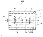
- FIG. 20 is a schematic plan view showing a power module according to Embodiment 4.
- FIG. 21 is a cross-sectional schematic diagram showing a power module according to Embodiment 4.
- FIG. 21 is a schematic cross-sectional view taken along the dashed-dotted line HH in FIG. 20.
- the power module 400 includes a lid portion 15, a pressure portion 14, a frame 16, a power semiconductor element 5, a solder 6 as a bonding material, an insulating substrate 7, and a heat spreader 8 as a heat diffusion portion. , wiring 9 as a connection wiring portion, bolts 4 and 11 as fastening members, and external connection terminals 10 .
- the metal layer 7c on the lower surface side of the insulating substrate 7 is joined to the upper surface of the heat spreader 8 via solder.
- the back surface of the power semiconductor element 5 is joined to the metal layer 7 a on the upper surface side of the insulating substrate 7 via solder 6 .
- Wiring 9 is joined to the surface of power semiconductor element 5 and metal layer 7 b on the upper surface side of insulating substrate 7 via solder 6 .
- External connection terminals 10 are joined to the upper surface of the metal layer 7a and the upper surface of the metal layer 7b on the upper surface side of the insulating substrate 7, respectively.
- the inner side surface of the frame 16 surrounding the insulating substrate 7 is in contact with the outer peripheral side surface of the heat spreader 8 .
- the lower surface of frame 16 is joined to the upper surface of the outer peripheral region of cooling unit 1 .
- a lid portion 15 is arranged on the upper surface of the frame body 16 .
- the lower surface of the lid portion 15 is in contact with the upper surface of the frame 16 .
- the outer edge of the heat spreader 8 is arranged inside the outer edge of the frame 16 .
- a pressurizing portion 14 is arranged between the lower surface of the lid portion 15 and the upper surface of the wiring 9, for pressurizing the solder 6 that joins the power semiconductor element 5 and the metal layer 7a.
- a sealing member 20 is arranged (filled) in the interior surrounded by the heat spreader 8 and the frame 16 .
- FIG. 20 is a schematic plan view of the power module 400 seen from the upper surface side through the cover 2.
- FIG. A transparent member is indicated by a dotted line.
- the outermost solid line is the outer edge of the lid portion 15 and the outer edge (outer wall) of the frame body 16 .
- An inner edge (inner wall) of the frame 16 is arranged inside the outer edge of the frame 16 .
- the outer edge of the heat spreader 8 is arranged inside the outer edge of the lid portion 15 (the outer edge of the frame 16).
- the outer edge of the insulating layer 7 d of the insulating substrate 7 is arranged inside the inner edge of the frame 16 .
- Metal layers 7 a and 7 b on the upper surface side of the insulating substrate 7 are arranged inside the outer edge of the insulating layer 7 d of the insulating substrate 7 .
- the power semiconductor element 5 and the external connection terminals 10 are arranged inside the outer edge of the upper surface of the metal layer 7 a on the upper surface side of the insulating substrate 7 .
- Wires 9 are arranged inside the outer edges of the upper surface of the power semiconductor element 5 and the metal layer 7b on the upper surface side of the insulating substrate 7, respectively.
- the wiring 9 is located inside the outer edge of the metal layer 7a and the metal layer 7b on the upper surface side of the insulating substrate 7, straddling the gap (spaced portion) between the outer edges of the metal layer 7a and the metal layer 7b facing each other. , the metal layer 7a and the metal layer 7b.
- a pressurizing portion 14 is arranged inside the inner edge of the frame 3 of the external connection terminal 10 protruding outside from the opposite side and on the upper surface of the wiring 9 .
- Fastening holes 2 b for arranging bolts 4 and 11 are arranged between the outer edge and the inner edge of the frame 16 .
- FIG. 21 is a schematic cross-sectional view of a portion corresponding to the external connection terminal 10 of the power module 400.
- FIG. 21 the metal layer 7c on the lower surface side of the insulating substrate 7 is joined to the upper surface of the heat spreader 8 via the solder 6.
- the back surface of the power semiconductor element 5 is joined to the metal layer 7 a on the upper surface side of the insulating substrate 7 via solder 6 .
- Wiring 9 is joined to the surface of power semiconductor element 5 and metal layer 7 b on the upper surface side of insulating substrate 7 via solder 6 .
- External connection terminals 10 are joined to the upper surface of the metal layer 7a and the upper surface of the metal layer 7b on the upper surface side of the insulating substrate 7, respectively.
- the external connection terminals 10 protrude to the outside of the power module 400 from the side surfaces of the frame bodies 16 facing each other.
- a region of the frame 16 where the external connection terminal 10 protrudes to the outside is provided with a hole or a notch through which the external connection terminal 10 protrudes to the outside. If the frame 16 is provided with a notch, the corresponding region of the lid 15 may be shaped to fit the notch of the frame 16 while holding the external connection terminal 10 therebetween.
- a frame 16 surrounding the insulating substrate 7 is arranged in the outer peripheral region of the upper surface of the heat spreader 8 .
- the lower surface of the frame 16 is joined to the upper surface of the cooling unit 1 , and the lower surface of the lid 15 is arranged on the upper surface of the frame 16 .
- a pressurizing portion 14 for pressurizing the solder 6 that joins the power semiconductor element 5 and the metal layer 7a is arranged.
- a sealing member 20 is arranged inside the frame 16 .
- the pressurizing part 14 extends in the first direction.
- the frame 16 is arranged in the outer peripheral region of the cooling unit 1 in contact with the inner surface of the frame 16 and the outer surface of the heat spreader 8 .
- the frame 16 is provided with a corner portion 3 c including the intersection of the top surface and the side surface of the heat spreader 8 .
- a corner portion 3c of the frame 16 is a fitting portion for fitting the frame 16 and the heat spreader 8 together.
- the frame 16 and the heat spreader 8 are arranged on the upper surface of the cooling section. Therefore, the lid portion 15 and the frame body 16 are fastened to the cooling portion 1 with bolts 4 and 11 . As a result, pressure is generated in the pressurizing section 14 .
- both the bolts 4 and 11 do not necessarily have to be used to fasten the lid portion 15 and the frame body 16 to the cooling portion 1, and only the bolt 4 may be used as long as the pressure required for pressurization can be obtained.
- At least the side of the pressurizing part 14 that contacts the upper surface of the wiring 9 is made of an insulating material.
- the upper surface of the pressurizing portion 14 is in contact with the lower surface of the lid portion 15 . If the pressurizing portion 14 that contacts the lid portion 15 made of the same material as the cooling portion 1 is entirely made of a metal member, the state from the power semiconductor element 5 to the lid portion 15 is not electrically insulated. As a result, the power module no longer functions. Therefore, in order to electrically insulate the wiring 9 and the lid portion 15, an insulating member is arranged at least on the side of the pressing portion 14 that is in contact with the upper surface of the wiring 9, thereby ensuring electrical insulation. It has a structure.
- the power semiconductor element 5 is attached to the metal layer 7a on the upper surface side of the insulating substrate 7.
- the joining solder 6 can be pressurized, and the occurrence of vertical cracks in the solder 6 can be suppressed. As a result, the reliability of power module 400 can be improved. Also, the life of the power module 400 can be extended.
- lid portion 15 and the frame body 16 are made of the same material as the cooling portion 1, heat generated in the power semiconductor element 5 or the external connection terminal 10 can be dissipated from the upper surface side of the power semiconductor element 5 as well. The heat dissipation of the module 400 can be improved.
- the pressure member 14 is provided between the lower surface of the lid portion 15 and the upper surface of the wiring 9 and the upper surface of the external connection terminal 10 .
- the solder 6 bonded to the metal layer 7a on the upper surface side of the can be pressurized, and the occurrence of vertical cracks in the solder 6 can be suppressed. As a result, reliability of the power module can be improved. Also, the life of the power module can be extended.
- lid portion 15 and the frame body 16 are made of the same material as the cooling portion 1, heat generated in the power semiconductor element 5 or the external connection terminal 10 can be dissipated from the upper surface side of the power semiconductor element 5 as well. It is possible to improve the heat dissipation of the module.
- Embodiment 5 the frame 16 used in the fourth embodiment is replaced with the frame 3 in which the heat radiating portion 17 is arranged on the outer wall region (outer surface) of the region sandwiched between the fastening holes 2b of the fastening member. is different. As described above, since the heat radiating portion 17 is arranged in the outer wall region of the region sandwiched between the fastening holes 2b for arranging the fastening member of the frame 3, the heat generated from the power semiconductor element 5 or the external connection terminal 10 is dissipated from the cooling portion 1.
- Heat can be dissipated to the outside by the frame 16 and the lid portion 15, and the heat generated in the power semiconductor element 5 and the external connection terminals 10 can be efficiently dissipated and the cooling capacity can be improved. Since other points are the same as those of the fourth embodiment, detailed description thereof will be omitted.
- FIG. 22 is a schematic plan view showing a power module according to Embodiment 5.
- FIG. FIG. 23 is a cross-sectional schematic diagram showing a power module according to Embodiment 5.
- FIG. FIG. 23 is a schematic cross-sectional view along the dashed-dotted line II in FIG.
- a power module 500 includes a lid portion 15, a pressurizing portion 14, a frame body 3 having a heat radiating portion 17 in an outer wall region, a power semiconductor element 5, a solder 6 as a bonding material, and an insulating substrate 7. , a heat spreader 8 that is a heat diffusion part, wiring 9 that is a connection wiring part, bolts 4 and 11 that are fastening members, and external connection terminals 10 .
- the metal layer 7c on the lower surface side of the insulating substrate 7 is joined to the upper surface of the heat spreader 8 via solder.
- the back surface of the power semiconductor element 5 is joined to the metal layer 7 a on the upper surface side of the insulating substrate 7 via solder 6 .
- Wiring 9 is joined to the surface of power semiconductor element 5 and metal layer 7 b on the upper surface side of insulating substrate 7 via solder 6 .
- External connection terminals 10 are joined to the upper surface of the metal layer 7a and the upper surface of the metal layer 7b on the upper surface side of the insulating substrate 7, respectively.
- a frame 3 surrounding the insulating substrate 7 is arranged in the outer peripheral region of the heat spreader 8 .
- the lower surface of frame 16 is joined to the upper surface of cooling unit 1 .
- the lower surface of the lid portion 15 is in contact with the upper surface of the frame 3 .
- the outer edge of the heat spreader 8 is arranged inside the outer edge of the frame 3 .
- a lid portion 15 is arranged on the upper surface of the frame 3 .
- the lower surface of the lid portion 15 is in contact with the upper surface of the frame 16 .
- a pressurizing portion 14 is arranged for pressurizing the solder 6 that joins the power semiconductor element 5 and the metal layer 7a.
- a heat radiating portion 17 is arranged in the outer wall region sandwiched between the fastening holes 2 b of the frame 3 .
- a sealing member 20 is arranged (filled) in the interior surrounded by the heat spreader 8 and the frame 3 .
- FIG. 22 is a schematic plan view of the power module 500 seen from the upper surface side through the lid portion 15.
- FIG. A transparent member is indicated by a dotted line.
- the outermost solid line is the outer edge of the lid portion 15 and the outer edge (outer wall) of the frame 3 .
- An inner edge (inner wall) of the frame 3 is arranged inside the outer edge of the frame 16 .
- the outer edge of the heat spreader 8 is arranged inside the outer edge of the lid portion 15 (the outer edge of the frame 3).
- the outer edge of the insulating layer 7 d of the insulating substrate 7 is arranged inside the inner edge of the frame 3 .
- Metal layers 7 a and 7 b on the upper surface side of the insulating substrate 7 are arranged inside the outer edge of the insulating layer 7 d of the insulating substrate 7 .
- the power semiconductor element 5 and the external connection terminals 10 are arranged inside the outer edge of the upper surface of the metal layer 7 a on the upper surface side of the insulating substrate 7 .
- Wires 9 are arranged inside the outer edges of the upper surface of the power semiconductor element 5 and the metal layer 7b on the upper surface side of the insulating substrate 7, respectively.
- the wiring 9 is located inside the outer edge of the metal layer 7a and the metal layer 7b on the upper surface side of the insulating substrate 7, straddling the gap (spaced portion) between the outer edges of the metal layer 7a and the metal layer 7b facing each other. , the metal layer 7a and the metal layer 7b.
- a pressurizing portion 14 is arranged inside the inner edge of the frame 3 of the external connection terminal 10 projecting outward from the opposite side and on the upper surface of the wiring 9 .
- Fastening holes 2 b for arranging bolts 4 and 11 are arranged between the outer edge and the inner edge of the frame 3 .
- a plate-shaped heat radiating portion 17 is arranged in a region (outer surface) on the outer edge side sandwiched between the fastening holes 2 b of the frame 3 .
- the heat radiating portion 17 is provided with fastening holes 2b on both sides, sandwiched between the fastening holes 2b, and spaced apart from the fastening holes 2b.
- the heat dissipation portion 17 is arranged to avoid the external connection terminals 10 on the side where the external connection terminals 10 protrude to the outside.
- the bolts 11 are used to fasten the cooling unit 1 , but the bolts 11 are not necessarily required, and the bolts 4 alone may be used to fasten the cooling unit 1 .
- the heat radiating portion 17 extending in the second direction may be arranged in a region sandwiched between the bolts 4 arranged to face each other in the second direction.
- FIG. 23 is a schematic cross-sectional view of a portion corresponding to the external connection terminal 10 of the power module 500.
- FIG. 23 the metal layer 7c on the lower surface side of the insulating substrate 7 is joined to the upper surface of the heat spreader 8 via the solder 6.
- the back surface of the power semiconductor element 5 is joined to the metal layer 7 a on the upper surface side of the insulating substrate 7 via solder 6 .
- Wiring 9 is joined to the surface of power semiconductor element 5 and metal layer 7 b on the upper surface side of insulating substrate 7 via solder 6 .
- External connection terminals 10 are joined to the upper surface of the metal layer 7a and the upper surface of the metal layer 7b on the upper surface side of the insulating substrate 7, respectively.
- the external connection terminals 10 protrude to the outside of the power module 500 from the side surfaces of the frame 3 facing each other.
- a region of the frame 3 where the external connection terminal 10 protrudes to the outside is provided with a hole or a notch through which the external connection terminal 10 protrudes to the outside.
- the lid 15 may have a shape that fits the notch of the frame 3 so that the external connection terminal 10 is sandwiched in the corresponding region.
- a frame 3 surrounding the insulating substrate 7 is arranged in the outer peripheral region of the upper surface of the heat spreader 8 .
- the lower surface of the frame 3 is joined to the upper surface of the heat spreader 8 , and the lower surface of the lid portion 15 is arranged on the upper surface of the frame 3 .
- a pressurizing portion 14 for pressurizing the solder 6 that joins the power semiconductor element 5 and the metal layer 7a is arranged.
- a sealing member 20 is arranged inside the frame 3 .
- a plate-shaped heat radiating portion 17 is arranged on the outer wall of the frame 3 .
- the heat radiating portion 17 has an upper surface in contact with the lower surface of the lid portion 15 and a lower surface in contact with the upper surface of the heat spreader 8 .
- the pressurizing part 14 extends in the first direction.
- a corner portion 3c of the frame 3 is a fitting portion for fitting the frame 3 and the heat spreader 8 together.
- the frame 3 and the heat spreader 8 can be easily positioned.
- the frame 3 and the heat spreader 8 are arranged on the upper surface of the cooling section.
- the lid portion 15 and the frame body 3 are fastened to the cooling portion 1 with bolts 4 and 11 .
- pressure is generated in the pressurizing section 14 .
- both the bolts 4 and 11 do not necessarily have to be used to fasten the lid portion 15 and the frame 3 to the cooling portion 1, and only the bolt 4 may be used as long as the pressure required for pressurization can be obtained.
- the power semiconductor element 5 is attached to the metal layer 7a on the upper surface side of the insulating substrate 7.
- the joining solder 6 can be pressurized, and the occurrence of vertical cracks in the solder 6 can be suppressed. As a result, the reliability of power module 500 can be improved. Also, the life of the power module 400 can be extended.
- heat radiating portion 17 is arranged on the outer wall region of the frame 3, heat generated by the power semiconductor element 5 or the external connection terminal 10 can be dissipated from the side surface of the power module 500 while maintaining insulation from the inside of the power module 500. Heat can be dissipated, and the heat dissipation of the power module 500 can be improved.
- the pressure member 14 is provided between the lower surface of the lid portion 15 and the upper surface of the wiring 9 and the upper surface of the external connection terminal 10 .
- the solder 6 bonded to the metal layer 7a on the upper surface side of the can be pressurized, and the occurrence of vertical cracks in the solder 6 can be suppressed. As a result, reliability of the power module can be improved. Also, the life of the power module can be extended.
- heat radiating portion 17 is arranged on the outer wall region of the frame 3, heat generated by the power semiconductor element 5 or the external connection terminal 10 can be dissipated from the side surface of the power module 500 while maintaining insulation from the inside of the power module 500. Heat can be dissipated, and the heat dissipation of the power module 500 can be improved.
- Embodiment 6 a power converter to which the power modules described in the first to fifth embodiments are applied will be described.
- the present disclosure is not limited to a specific power converter, a case where the present disclosure is applied to a three-phase inverter will be described below as a sixth embodiment.
- FIG. 24 is a block diagram showing the configuration of a power conversion system to which the power converter according to this embodiment is applied.
- the power conversion system shown in FIG. 24 comprises a power supply 1000, a power conversion device 2000, and a load 3000.
- the power supply 1000 is a DC power supply and supplies DC power to the power converter 2000 .
- the power supply 1000 can be composed of various things, for example, it can be composed of a DC system, a solar battery, and a storage battery. Alternatively, it may be composed of a rectifier circuit or an AC/DC converter connected to an AC system. Also, power supply 1000 may be configured with a DC/DC converter that converts DC power output from a DC system into predetermined power.
- the power conversion device 2000 is a three-phase inverter connected between the power supply 1000 and the load 3000, converts the DC power supplied from the power supply 1000 into AC power, and supplies the AC power to the load 3000. As shown in FIG. 24, the power conversion device 2000 includes a main conversion circuit 2001 that converts DC power into AC power and outputs it, and a control circuit 2003 that outputs a control signal for controlling the main conversion circuit 2001 to the main conversion circuit 2001. and
- a load 3000 is a three-phase electric motor driven by AC power supplied from the power converter 2000 .
- the load 3000 is not limited to a specific application, but is an electric motor mounted on various electrical equipment, such as a hybrid vehicle, an electric vehicle, a railway vehicle, an elevator, or an electric motor for an air conditioner.
- the main conversion circuit 2001 includes a switching element and a freewheeling diode (not shown). By switching the switching element, DC power supplied from power supply 1000 is converted into AC power and supplied to load 3000 .
- the main conversion circuit 2001 has various specific circuit configurations, the main conversion circuit 2001 according to the present embodiment is a two-level three-phase full bridge circuit, and has six switching elements and It can consist of six freewheeling diodes in anti-parallel.
- each switching element and each freewheeling diode of the main conversion circuit 2001 is a switching element or a freewheeling diode included in the power module 2002 corresponding to the power module according to at least one of the first to fifth embodiments described above.
- the six switching elements constitute upper and lower arms connected in series for every two switching elements, and each upper and lower arm constitutes each phase (U phase, V phase, W phase) of the full bridge circuit.
- Output terminals of the upper and lower arms, that is, three output terminals of the main conversion circuit 2001 are connected to the load 3000 .
- the main conversion circuit 2001 includes a drive circuit (not shown) for driving each switching element. may be provided.
- the drive circuit generates a drive signal for driving the switching element of the main conversion circuit 2001 and supplies it to the control electrode of the switching element of the main conversion circuit 2001 .
- a drive signal for turning on the switching element and a drive signal for turning off the switching element are output to the control electrode of each switching element.
- the driving signal is a voltage signal (ON signal) equal to or higher than the threshold voltage of the switching element, and when maintaining the switching element in the OFF state, the driving signal is a voltage equal to or less than the threshold voltage of the switching element. signal (off signal).
- the control circuit 2003 controls the switching elements of the main conversion circuit 2001 so that the desired power is supplied to the load 3000 . Specifically, based on the power to be supplied to the load 3000, the time (on time) during which each switching element of the main converter circuit 2001 should be in the ON state is calculated. For example, the main conversion circuit 2001 can be controlled by PWM control that modulates the ON time of the switching element according to the voltage to be output. Then, a control command (control signal) to the drive circuit provided in the main conversion circuit 2001 so that an ON signal is output to the switching element that should be in the ON state at each time point, and an OFF signal is output to the switching element that should be in the OFF state at each time. to output The drive circuit outputs an ON signal or an OFF signal as a drive signal to the control electrode of each switching element according to this control signal.
- the power modules according to Embodiments 1 to 5 are applied as the power module 2002 forming the main conversion circuit 2001 .
- longitudinal cracks in the solder 6 that joins the power semiconductor element 5 to the insulating substrate 7 can be suppressed.
- the reliability of power converter 2000 can be improved.
- the present disclosure is not limited to this, and can be applied to various power converters.
- a two-level power conversion device is used, but a three-level or multi-level power conversion device may be used. Disclosure may apply.
- the present disclosure can be applied to a DC/DC converter or an AC/DC converter when power is supplied to a DC load or the like.
- the power conversion device to which the present disclosure is applied is not limited to the case where the above-described load is an electric motor. It can also be used, and furthermore, it can be used as a power conditioner for a photovoltaic power generation system, an electric storage system, or the like.
- Cooling part 2, 15 Lid part, 2a, 14 Pressure part, 2b Fastening hole, 3, 16 Frame, 3c Corner of frame 3, 4, 11 Bolt, 5 Power semiconductor element, 6 Solder, 7 Insulating substrate 7a, 7b, 7c Metal layer 7d Insulating layer 8 Heat spreader 9 Wiring 10 External connection terminal 12 Heat spreader top surface 13 Heat spreader side surface 17 Radiation part 20 Sealing member 100, 101, 200 , 300, 400, 500, 2002 power module, 1000 power supply, 2000 power converter, 2001 main conversion circuit, 2003 control circuit, 3000 load.
Landscapes
- Cooling Or The Like Of Semiconductors Or Solid State Devices (AREA)
Abstract
接合材を加圧する加圧部を備え、信頼性を向上させたパワーモジュールを得る。熱拡散部(8)と、熱拡散部(8)の上面上に接合材(6)で接合され、上面と下面との金属層(7a,7c)を有する絶縁基板(7)と、絶縁基板(7)の上面上に接合材(6)で接合された半導体素子(5)と、半導体素子(5)の上方に配置され、半導体素子(5)と接続された接続配線部(9)と、絶縁基板(7)を囲み、熱拡散部(8)の外周領域に配置された枠体(3)と、枠体(3)の上面側に配置される蓋部(2)と、蓋部(2)と接続配線部(9)との間に配置され、接続配線部(9)を介して半導体素子(5)を加圧する加圧部(2a)と、蓋部(2)と枠体(3)とを熱拡散部(8)に締結する締結部材(4,11)と、を備えたパワーモジュールである。
Description
本開示は、接合材を加圧する加圧部を備えたパワーモジュールおよび電力変換装置に関する。
パワーモジュールに実装されるパワー半導体素子は、主電流を高速でスイッチングするために、高温状態または高温と低温の状態を行き来する温度サイクルに曝される。このような高温状態または温度サイクルに曝されると、パワーモジュールの各構成部材は、それぞれの線膨張係数の差により、各構成部材の接合部への高い応力負荷が発生する。特に、接合材としてはんだを用いたはんだ接合部には、クラックが入ったりし、劣化が発生しやすい。
線膨張係数が大きく異なる部材同士である、例えば、シリコン(Silicon:Si)のパワー半導体素子と銅基板とをはんだで接合する場合、はんだ接合部に高いせん断応力が発生し、はんだ外周部から中央部に向かって接合面とほぼ平行にクラックが進展していく、いわゆる「横割れ」が発生する。はんだ内部で横割れが発生し進展すると、はんだ接合部での接合面積が減少し、パワー半導体素子で発生した熱を外部に放出するための熱抵抗が大きくなり、パワー半導体素子などが破壊される。この問題を避けるためには、はんだ接合される被接合部材間の線膨張係数の差を小さくすることが好ましい。この結果、発生する熱応力が小さくなり、接合部の不良の発生は大幅に低減され、横割れを抑制することができる。
ところが、被接合部材間の線膨張係数の差が小さくなったパワーモジュールに温度サイクルが印加されると、はんだ接合部の中央付近に、接合面に対して平行方向の等2軸の引張圧縮変形による連続動的再結晶によって形成される高Σ粒界でき裂が発生、進展することで、最終的にき裂のネットワークを形成する破壊が発生する。これは、き裂が発生する段階で、接合面に対して垂直方向にき裂が進展するので、いわゆる「縦割れ」と呼ばれている。
このため、従来のパワーモジュールでは、チップ上に絶縁材料を挟んで、チップ面への圧力を加えるための押さえ板を配置し、縦割れを防ぐことではんだ中央部のクラック発生を抑制することが記載されている(例えば、特許文献1)。
しかしながら、特許文献1に記載のパワーモジュールにおいては、ワイヤとパワー半導体素子の表面との間に押さえ板を配置し、押さえ板自体を加圧するための部材が別途必要であった。このため、はんだ接合部に十分な加圧力を発生させることができず、パワーモジュールの信頼性が劣化する場合があった。
本開示は、上述のような問題を解決するためになされたもので、蓋と配線部材との間に加圧部を設けて接合部を加圧することで、信頼性の向上したパワーモジュールを得ることを目的としている。
本開示に係るパワーモジュールは、熱拡散部と、熱拡散部の上面上に接合材で接合され、上面と下面との金属層を有する絶縁基板と、絶縁基板の上面上に接合材で接合された半導体素子と、半導体素子の上方に配置され、半導体素子と接続された接続配線部と、絶縁基板を囲み、熱拡散部の外周領域に配置された枠体と、枠体の上面側に配置される蓋部と、蓋部と接続配線部との間に配置され、接続配線部を介して半導体素子を加圧する加圧部と、蓋部と枠体とを熱拡散部に締結する締結部材と、を備えたパワーモジュールである。
本開示によれば、枠体の上面側に配置される蓋部と、蓋部と接続配線部との間に配置され、接続配線部を介して半導体素子を加圧する加圧部と、蓋部と枠体とを熱拡散部に締結する締結部材とを設けたので、半導体素子と絶縁基板の上面の金属層とを接合する接合部を加圧することが可能となり、パワーモジュールの信頼性を向上させることができる。
はじめに、本開示のパワーモジュールの全体構成について、図面を参照しながら説明する。なお、図は模式的なものであり、示された構成要素の正確な大きさなどを反映するものではない。また、同一の符号を付したものは、同一又はこれに相当するものであり、このことは明細書の全文において共通することである。各図には、第1方向(X方向)と第2方向(Y方向)と第3方向(Z方向)とを示している。
実施の形態1.
図1は、実施の形態1におけるパワーモジュールを示す平面構造模式図である。図2は、実施の形態1におけるパワーモジュールを示す断面構造模式図である。図3は、実施の形態1におけるパワーモジュールを示す断面構造模式図である。図4は、実施の形態1におけるパワーモジュールを示す断面構造模式図である。図5は、実施の形態1におけるパワーモジュールを示す断面構造模式図である。図6は、実施の形態1における他のパワーモジュールを示す断面構造模式図である。図2は、図1の一点鎖線AAにおける断面構造模式図である。図3は、図1の一点鎖線BBにおける断面構造模式図である。図4は、図1の一点鎖線CCにおける断面構造模式図である。図5は、パワーモジュール100に冷却部1を取り付けた場合の図1の一点鎖線AAにおける断面構造模式図である。図6は、パワーモジュール100に冷却部1を取り付けた場合の図1の一点鎖線AAにおける断面構造模式図で、封止部材10の上面の高さが配線9の高さと同じ場合である。
図1は、実施の形態1におけるパワーモジュールを示す平面構造模式図である。図2は、実施の形態1におけるパワーモジュールを示す断面構造模式図である。図3は、実施の形態1におけるパワーモジュールを示す断面構造模式図である。図4は、実施の形態1におけるパワーモジュールを示す断面構造模式図である。図5は、実施の形態1におけるパワーモジュールを示す断面構造模式図である。図6は、実施の形態1における他のパワーモジュールを示す断面構造模式図である。図2は、図1の一点鎖線AAにおける断面構造模式図である。図3は、図1の一点鎖線BBにおける断面構造模式図である。図4は、図1の一点鎖線CCにおける断面構造模式図である。図5は、パワーモジュール100に冷却部1を取り付けた場合の図1の一点鎖線AAにおける断面構造模式図である。図6は、パワーモジュール100に冷却部1を取り付けた場合の図1の一点鎖線AAにおける断面構造模式図で、封止部材10の上面の高さが配線9の高さと同じ場合である。
図において、パワーモジュール100は、蓋部2と、加圧部2aと、枠体3と、半導体素子であるパワー半導体素子5と、接合材(接合部)であるはんだ6と、絶縁基板7と、熱拡散部であるヒートスプレッダ8と、接続配線部である配線9と、締結部材であるボルト4,11と、外部接続端子10と、を備えている。
図において、ヒートスプレッダ8の上面には、絶縁基板7の下面側の金属層7cがはんだ6を介して接合されている。絶縁基板7の上面側の金属層7aには、パワー半導体素子5の裏面がはんだ6を介し接合されている。パワー半導体素子5の表面と絶縁基板7の上面側の金属層7bとには、配線9がはんだ6を介して接合されている。また、絶縁基板7の上面側の金属層7aの上面と金属層7bの上面とには、それぞれ外部接続端子10が接合されている。ヒートスプレッダ8の上面の外周領域には、絶縁基板7を囲む枠体3が配置される。枠体3の下面は、ヒートスプレッダ8の上面と接合されている。枠体3の上面には、蓋部2が配置される。蓋部2の下面と配線9の上面との間には、パワー半導体素子5と金属層7aとを接合するはんだ6を加圧するための加圧部2aが配置されている。ヒートスプレッダ8と枠体3とで囲まれた内部には、封止部材20が配置(充填)される。
図1は、パワーモジュール100を上面側から蓋部2を透過して見た平面構造模式図である。透過した部材に関しては、点線にて表示している。
図1において、最外周の実線は、蓋部2の外縁および枠体3の外縁(外壁)である。枠体3の外縁よりも内側には、枠体3の内縁(内壁)が配置されている。ヒートスプレッダ8の外縁は蓋部2の外縁(枠体3の外縁)と同じ位置に配置されている。枠体3の内縁よりも内側には、絶縁基板7の絶縁層7dの外縁が配置されている。絶縁基板7の絶縁層7dの外縁よりも内側には、絶縁基板7の上面側の金属層7a,7bが配置されている。
絶縁基板7の上面側の金属層7aの上面の外縁の内側には、パワー半導体素子5と外部接続端子10(実線)とが配置される。パワー半導体素子5の上面と絶縁基板7の上面側の金属層7bの外縁よりも内側には、配線9がそれぞれ配置されている。配線9は、絶縁基板7の上面側の金属層7aと金属層7bとの外縁よりも内側で、金属層7aと金属層7bとの外縁の対向する間の隙間部(離間部)を跨いで、金属層7aと金属層7bとに配置されている。パワー半導体素子5の外縁よりも内側で、パワー半導体素子5の上方にある配線9には、加圧部2aが配置されている。枠体3の外縁と内縁との間には、ボルト4,11を配置するための締結用穴2bが配置されている。
図2は、パワーモジュール100の冷却部1と締結するための締結用穴2bに対応する部分の断面模式図である。図2において、ヒートスプレッダ8の上面には、絶縁基板7の下面側の金属層7cがはんだ6を介して接合されている。絶縁基板7の上面側の金属層7aには、パワー半導体素子5の裏面がはんだ6を介し接合されている。パワー半導体素子5の表面と絶縁基板7の上面側の金属層7bの上面とには、配線9がはんだ6を介して接合されている。また、絶縁基板7の上面側の金属層7aの上面と金属層7bの上面とには、それぞれ外部接続端子10が接合されている。
ヒートスプレッダ8の上面の外周領域には、絶縁基板7を囲む枠体3が配置される。枠体3の下面は、ヒートスプレッダ8の上面と接合されている、枠体3の上面には、蓋部2が配置される。蓋部2の下面側と配線9の上面との間には、パワー半導体素子5と金属層7aとを接合するはんだ6を加圧するための加圧部2aが配置されている。枠体3の内部には、封止部材20が配置される。枠体3と蓋部2とヒートスプレッダ8との対応する箇所には、ボルト4を挿入するための、締結用穴2bが配置されている。締結用穴2bは、蓋部2と枠体3とヒートスプレッダ8とを貫通して形成されている。外部接続端子10は、蓋部2の所定の位置を貫通して蓋部2の外部へ突出している。
図3は、パワーモジュール100のヒートスプレッダ8との締結のための締結用穴2bに対応する部分の断面模式図である。図3において、図2との違いは、締結部材4を挿入する締結用穴2bの形状である。図3においては、締結用穴2bの底部は、ヒートスプレッダ8を貫通しておらず、ヒートスプレッダ8の内部で止まった形状である。
図4は、パワーモジュール100のパワー半導体素子5を加圧部2aで加圧する領域に対応する部分の断面模式図である。図4において、絶縁基板7の上面側の金属層7aの上面には、接合材であるはんだ6を介してパワー半導体素子5の裏面が接合されている。パワー半導体素子5の表面には電極(図示せず)が形成されており、はんだ6を介して配線9の下面とパワー半導体素子5の電極が接合されている。パワー半導体素子5の上方であり、配線9の上面には、加圧部2aが配置されている。加圧部2aは、下面が配線9の上面に接し、上面が蓋部2の下面と接して配置される。このように、パワー半導体素子5と配線9と加圧部2aと蓋部2とが直線的(直列)に配置されることで、蓋部2をヒートスプレッダ8にボルト11を用いて締結することでパワー半導体素子5を絶縁基板7の上面側の金属層7aに接合しているはんだ6を加圧することができる。
図5は、パワーモジュール100に冷却部1を取り付けた断面構造模式図である。図5において、ヒートスプレッダ8の下面と接するように冷却部1の上面が配置される。冷却部1は、ボルト4によりパワーモジュール100と締結される。ボルト11での締結ではんだ6への加圧力が足りない場合は、ボルト4での締結時に加圧力を増加させることができる。
ヒートスプレッダ8は、板状であり、絶縁基板7等を内包するパワーモジュール100の底面部(底板)である。ヒートスプレッダ8は、第1方向と第2方向とに延在している。ヒートスプレッダ8は、パワーモジュール100の内部で発生した熱をパワーモジュール100の外部へ放熱するための熱拡散部材として機能する。ヒートスプレッダ8は、ヒートスプレッダ8の上面が絶縁基板7の下面側の金属層7cの下面と、接合材であるはんだ6を介して(用いて)接合されている。ヒートスプレッダ8の材料としては、銅合金またはアルミニウム合金などを用いることができる。ヒートスプレッダ8の上面ではんだ6との接合領域の外側には、封止部材20の下面が接している。ヒートスプレッダ8の材料としては、銅(Cu)またはアルミニウム(Al)などの熱伝導性のよい金属またはグラファイト素材などの材料を用いることができる。
絶縁基板7は、第1方向と第2方向とに延在している。絶縁基板7は、板状の部材である。絶縁基板7は、上面層と中間層と下面層とを有している。絶縁基板7の下面側の金属層7cは、ヒートスプレッダ8の上面に対向している。絶縁基板7は、中間層として絶縁層7d、上面層として絶縁層7dの上面側に金属層7aと、下面層として絶縁層7dの下面側に金属層7cと、を有している。絶縁層7dの下面側の金属層7cは、はんだ6によりヒートスプレッダ8の上面と接合されている。絶縁基板7は板状であり、板状の絶縁基板7を平面(上面)方向から見た場合において、絶縁層7dの上面側の金属層7aの大きさは、絶縁層7dの大きさよりも小さくなっている。絶縁層7dの下面側の金属層7cの大きさは、絶縁層7dの大きさよりも小さくなっている。絶縁層7dの端部は、絶縁層7dの上面側の金属層7aおよび絶縁層7dの下面側の金属層7cの端部よりも外側へ突出している。この構成は、絶縁層7dを挟んで、絶縁層7dの上面側の金属層7aが、絶縁層7dの下面側の金属層7cおよびヒートスプレッダ8との間で沿面放電を抑制(沿面距離を確保)するためである。
また、絶縁層7dの上面側の金属層7aは、目的に応じて複数に分割され、回路パターンを形成してもよい。図1においては、金属層7aには、パワー半導体素子5と外部接続端子10とが配置されている。金属層7bには、配線の一旦と外部接続端子10とが配置されている。絶縁基板7の絶縁層7dの材料としては、酸化アルミニウム(Al2O3)、窒化アルミニウム(AlN)または窒化珪素(Si3N4)などのセラミック基板が用いることができる。絶縁層7dの上面には、ロウ付けまたは直接接合などの方法を用いて、金属層(回路パターン板)7aと金属層(中継板)7bとが接合されている。また、絶縁層7dの下面には、ロウ付けまたは直接接合などの方法を用いて、金属層(放熱用板)7cが接合されている。絶縁基板7の上面側の金属層7aおよび下面側の金属層7cの材料としては、CuまたはAl等の電気の良導体であればなんでも使用することができる。また、CuとAlとを積層して2層構造になった材料を、それぞれ金属層7a、金属層7b、金属層7cとして使用してもよい。2層構造の絶縁基板7を用いる場合、Alは、Cuと絶縁基板7との接合の応力緩和層となるため、絶縁層7dに近い側がAl層、遠い側はCu層である。なお、絶縁基板7の上面側は、絶縁層7dの上面側、絶縁基板7の下面側は、絶縁層7dの下面側と同義である。
パワー半導体素子5は、パワー半導体素子5の表面に電極(図示せず)が配置された構造である。パワー半導体素子5は、絶縁基板7の上面側の金属層7aの上面に接合部であるはんだ6を介して接合されている。 パワー半導体素子5の材料としては、例えば、珪素(Si:Silicon)、炭化珪素(SiC:Silicon Cabide)、および窒化ガリウム(GaN:Gallium Nitride)を用いることができる。また、パワー半導体素子5は、MOSFET(Metal Oxide Semiconductor Field Effect Transistor)、IGBT(Insulated Gate Bipolar Transistor)、FWD(Free Wheel Diode)、およびRC-IGBT(Reverse Conducting IGBT)などのパワーデバイスである。
配線9は、板状の金属部材である。配線9は、一端が絶縁基板7の上面側の金属層7aのパワー半導体素子5の電極と電気的に接続している。また、配線9は、他端が金属層7bの所定の位置と電気的に接続している。配線9は、パワー半導体素子5の電極とはんだ6を介して接続されている。また、配線9は、金属層7bとはんだ6を介して接続されている。配線9は、十分な剛性のある良導体の金属でできており、例えば、銅板が使用可能である。また、配線9の材料として、Alを用いた場合には、Alの表面にニッケル(Ni)めっきなどのはんだ接合ができるような構成にすれば使用可能である。さらに、配線9は、両端ともはんだ6で接合しているが、超音波接合などで接合されてもよい。また、配線9は、十分な剛性の得られるCuリボン材、Alリボン材などを使用することができる。配線9は、パワー半導体素子5または金属層7bと超音波接合を用いて接合してもよい。
外部接続端子10は、一端が金属層7aの所定の位置と金属層7bの所定の位置とを超音波接合を用いて接合されている。また、外部接続端子10は、他端が枠体3の側面部に設けられた貫通孔から外部に取り出されている(突出している)。外部接続端子10は、枠体3の側面部と図示しない絶縁ブッシュを挿入して沿面絶縁距離を長く確保する構造とすることも可能である。外部接続端子10は、図2では枠体3の側面部に設けられた貫通孔からパワーモジュール100の外部へ突出している。例えば、後述する図14のような枠体3の側面部に貫通孔または切り欠きを設けてパワーモジュール100の外部へ取り出してもよい。外部接続端子10は、金属層7aまたは金属層7bと超音波接合を用いて接合しているが、はんだを用いて接合してもよい。
枠体3および蓋部2は、PPS樹脂(Poly Phenylene Sulfide Resin)などの高い剛性のある樹脂などを使用することができる。また、枠体3および蓋部2は、剛性を高めるたにCu、Alおよびステンレスなどの剛性の高い金属を使用してもよい。枠体3および蓋部2として金属材を使用する場合は、枠体3および蓋部2の表面を樹脂でコーティングして絶縁を確保する必要がある。本実施の形態では、蓋部2は、蓋部2のパワーモジュール100の内部側(配線9の上面側)に突起した加圧部2aを有している。
加圧部2aは、加圧部2aの下面が配線9と接触するので、より絶縁を高めるためには、加圧部2aの材料である樹脂材のコーティング量を増やす、またはセラミックなどの絶縁体を加圧部2aの先端(下面)に配置するとよい。また、加圧部2aとして金属材を使用している場合には、ボルト4,11を挿入する締結用穴2bの内面にも樹脂を厚くコーティングする、または、絶縁ブッシュ材を挿入して、沿面絶縁距離を長く確保するとよい。
枠体3は、絶縁基板7を取り囲む枠体である。加圧部2aは、蓋部2と一体として形成されていてもよく、蓋部2と別体として形成されていてもよい。蓋部2の下面側の形状としては、枠体3の上面と接する同一平面であればよい。また、蓋部2の下面側の形状としては、枠体3の内縁よりも内側でヒートスプレッダ8方向へ突出していてもよい。このような形状であれば、蓋部2の下面が加圧部2aの上面と接することができるので、パワー半導体素子5を接合するはんだ6を確実に加圧することが可能である。蓋部2および枠体3に設けている締結用穴2bは、締結に用いるボルト4,11の大きさ(太さ)に合わせて適宜形成されていればよい。蓋部2と枠体3とヒートスプレッダ8と冷却部1とを締結でき、加圧部2aに必要な加圧力を加えることができれば、大きさは特に限定されない。
ボルト4は、ヒートスプレッダ8を貫通して、蓋部2と枠体3とを冷却部1に締結する。また、ボルト11は、蓋部2と枠体3とをヒートスプレッダ8に締結する。ボルト4,11は、蓋部2および枠体3に設けられた締結用穴2bを通して(挿入して)、蓋部2および枠体3をヒートスプレッダ8または冷却部1に適切な締め付け力で締結する。このとき、ヒートスプレッダ8と冷却部1との間には、図示しない熱伝導グリースまたはグラファイトシートなどを間に介して、熱抵抗を下げている。ここで、ボルト4の頭部は、蓋部2の中に埋め込まれた構造になっているが、図13に示すような蓋部2の外側に頭部を出している構造になっていてもよい。ボルト4,11としては、一般的なボルトを使用することができる。
接合材6は、ヒートスプレッダ8と絶縁基板7と、絶縁基板7とパワー半導体素子5とおよび絶縁基板7と配線9とを接合する。接合材であるはんだ6は、錫(Sn)系のはんだを使用することができる。また、このようなSn系はんだには、応力緩和性、耐熱性および耐疲労強度を持たせるため、アンチモン(Sb)、銀(Ag)およびCuなどを添加し、任意の組成とすることができる。はんだ6は、被接合部材と一緒にリフローすることで、被接合部材と被接合部材とを接合する。ダイボンディング用の接合材としては、一般的なはんだを例に説明したが、はんだの他に、TLP接合(Transient Liquid Phase:遷移的液相焼結法)、AgまたはCuなどのナノ粒子を利用した焼結型の接合材もあり、本開示にも適用できるが、低コスト化およびプロセスの安定性からは、はんだ材が最も適している。
封止部材20は、枠体3内部に充填されている。封止部材20は、絶縁基板7とパワー半導体素子5とを封止する。封止部材20の材料としては、シリコーンゲルまたはシリカなどのフィラを含むエポキシ樹脂を使用することができる。特に、封止部材20の材料としてシリコーンゲルを用いた場合は、加圧部2aでの加圧効果が十分に発揮される。封止部材20の上面は、配線9の上面と同じ高さ(図6)から蓋部2の下面に接する高さ(図5)までの範囲で枠体3の内部に充填することができる。封止部材20の上面の高さが配線9の上面よりも高い場合、予め加圧部2aが配置される領域に、ダミーとなる部材を配置してから封止部材20を充填することで、加圧部2aの配置領域を確保することができる。この場合、配線9は、加圧部2aの配置位置以外は、封止部材20で封止される。また、封止部材20の上面は、配線9の上面と同じ高さの場合は、外部接続端子10との距離を確保しておくことが望ましい。配線9と外部接続端子10との距離の確保が難しい場合は、封止部材20の上面の高さは、配線9の上面を覆う高さとするほうがよい。この場合、使用するパワーモジュールの電圧にもよるが、配線9の上面を覆う封止部材20の厚さとしては、少なくとも100μmは必要である。なお、配線9の上面を覆う封止部材20の厚さは、100μm以上の範囲で使用するパワーモジュールの電圧に応じて適宜選択可能である。
冷却部1は、平板状の金属部材である。冷却部1の材料としては、CuまたはAl等を使用することができる。冷却部1の形態としては、平板だけではなく、ウォータージャケットまたはヒートシンクなどを用いてもよい。図5に図示した冷却部1は、ウォータージャケットまたはヒートシンクの天板を摸擬して表示しており、冷却部1の天板以外の構成はどのような構成でもよい。冷却部1として、ヒートシンクを用いる場合には、冷却の方法として空冷だけでなく、水冷または液冷を用いてもよい。
なお、本開示では、パワー半導体素子5を接合するはんだ6へのせん断応力を低減するために、パワー半導体素子5と絶縁基板7との間の線膨張係数の差は小さく、望ましくは5ppm/K以下として、はんだ6の内部を水平方向に進展するクラックの横割れを抑制する対策を実施している。
このようなはんだ6の横割れ対策を施して、線膨張係数差の小さい構造にした場合においても、各構成部材に温度ストレスが繰り返し加わることで、各構成部材は膨張と収縮を繰り返し、応力負荷を発生させ、はんだ6などの接合部を劣化させる。この劣化は、はんだ接合部の中央付近に、接合面に対して平行方向の等2軸の引張圧縮変形により連続動的再結晶によって形成される高Σ粒界で、き裂が発生・進展して、網目状に周辺部へ拡大し、最終的にき裂のネットワークを形成する破壊が発生する。これは、き裂が発生する段階で、接合面に対して垂直方向にき裂が進展するので、いわゆる「縦割れ」と呼ばれている。このような縦割れが発生すると、熱抵抗または電気抵抗を上昇される要因となり、最終的には、パワーモジュールの故障へとつながる。
そして、はんだ6の縦割れが発生すると、はんだ6の厚さが接合した初期の厚さと比較し、増加していることが確認されている。
しかしながら、本実施の形態1では、等2軸の引張圧縮変形によるき裂の発生を抑制するために、蓋部2の下面側の加圧部2aで配線9を介してはんだ6を加圧している。このように、はんだ6を加圧することにより、等2軸の引張圧縮変形ではなくなるので、はんだ6の縦割れを抑制できる。
このように、加圧部2aを用いてパワーモジュール100を構成したので、パワー半導体素子5を絶縁基板7の上面側の金属層7aに接合しているはんだ6の縦割れの発生を抑制することができ、パワー半導体素子5の動作時の放熱を遮ることないため、パワーモジュール100の信頼性が向上できる。また、パワーモジュール100の寿命を長寿命化できる。
また、外部接続端子10は、パワーモジュール100の上面となる蓋部2からパワーモジュール100の外部へ突出しているので、パワーモジュールの小型化が可能となる。
図7は、実施の形態1における他のパワーモジュールを示す断面構造模式図である。図7は、冷却部1にボルト4でヒートスプレッダ8を取り付けた断面図である。図7において、パワーモジュール100と異なりパワーモジュール101は、ヒートスプレッダ8が、枠体3の外縁まで伸びておらず、ヒートスプレッダ8の外側面と枠体3の内側面とが接する枠体3の角部3cが形成されている。枠体3の角部3cは、枠体3とヒートスプレッダ8とを嵌合する嵌合部である。枠体3の角部3cを設けることで、枠体3とヒートスプレッダ8との位置決めを容易に行うことができる。
次に、本実施の形態に記載のパワーモジュール100の製造方法について説明する。
図8から図13は、実施の形態1におけるパワーモジュールの製造工程を示す断面構造模式図である。
本実施の形態1の主要な製造工程は、大きく分けて5つ工程である。第一工程としては、絶縁基板7上にパワー半導体素子5等を接合する(絶縁基板への実装工程)。第二工程としては、パワー半導体素子5等を接合した絶縁基板7と枠体3とをヒートスプレッダ8上に接合する(ヒートスプレッダへの実装工程)。第三工程としては、ヒートスプレッダ8と枠体3とで囲まれた領域内に封止部材20を充填する(枠体内樹脂充填工程)。第四工程としては、封止部材20が充填された枠体3に蓋部2を配置する(蓋部締結工程)。第五工程としては、ヒートスプレッダ8と冷却部1とを締結する(冷却部締結工程)。これらの工程を経ることで、冷却部1を備えたパワーモジュール100が製造できる。
はじめに、図8に示すように、絶縁基板7の上面側の金属層7a,7b上の所定の位置に、パワー半導体素子5と配線9と外部接続端子10とを接合(配置)する(絶縁基板への実装工程)。パワー半導体素子5、配線9の接合には、接合材としてはんだ6が用いられる。外部接続端子10の絶縁基板7の上面側の金属層7a,7bへの接合は、はんだ6または超音波接合で行うことができる。
次に、図9に示すように、パワー半導体素子5等が配置された絶縁基板7をヒートスプレッダ8の上面に接合(配置)する。また、ヒートスプレッダ8の上面の外周領域には、枠体3が絶縁基板7を囲んで配置される(ヒートスプレッダへの実装工程)。絶縁基板7の接合には、通常、はんだが用いられる。また、枠体3の接着(接合)には、通常、接着剤が用いられる。
次に、図10に示すように、絶縁基板7が配置され、枠体3とヒートスプレッダ8とで囲まれた領域内に封止部材20を充填する。封止部材20の上面のヒートスプレッダ8の上面からの高さは、配線9の上面から枠体3の上面、言い換えると、蓋部2の下面と接する高さまでの範囲で充填することができる。配線9の上面よりも高い位置まで封止部材20を充填する場合、加圧部2aが蓋部2と一体で形成されていれば、予め加圧部2aを配置する領域を確保するために、ダミー部材を配置しておくほうがよい(枠体内の樹脂充填工程)。加圧部2aが蓋部2と別体で形成されていれば、加圧部2aを予め配線9の上面の所定の位置に配置してから、封止部材20を充填してもよい。なお、封止部材20の上面が蓋部2の下面と接していない場合の一例として、図6に示したように、配線9の上面と同じ高さとする場合は、配線9の上面と同じ高さになるように、封止部材20を充填する。また、必要に応じて、封止部材20の高さは、配線9の上面から蓋部2の下面までの範囲で適宜選択可能である。
次に、図11に示すように、封止部材20が充填された枠体3の上面上に蓋部2を配置し、ボルト11を用いて蓋部2と枠体3とをヒートスプレッダ8に締結する。本実施の形態1では、加圧部2aは蓋部2の下面から突出して配置されている。このように、ボルト11を用いて蓋部2を締結することで、矢印で示す方向に配線9を介して加圧部2aからパワー半導体素子5と絶縁基板7の上面側の金属層7aとを接合するはんだ6に圧力が加わることとなる(蓋部締結工程)。ここで、図11は、便宜上、断面位置として図1における断面AA(図2)と断面BB(図3)とを合わせた表示となっている。なお、図12には、冷却部1と締結するためのボルト4を挿入する締結用穴2bでの断面形状である。
次に、図13に示すように、必要に応じて、ヒートスプレッダ8の下面と冷却部1の上面とを接続するヒートスプレッダ8と冷却部1との接続は、ボルト4を用いて行う(冷却部締結工程)。このように、ボルト4を用いて締結する場合でも、矢印で示した方向(Z方向で加圧部2aから絶縁基板7へ向かう方向)に圧力を加えることができる。なお、ヒートスプレッダ8と冷却部1との間には、熱伝導性をよくするために、図示していない熱伝導性材料TIM(Thermal Interface Material)やグラファイトシートなど挟んで効率よく放熱してもよい。
これらの工程を経ることで、冷却部1を備えたパワーモジュール100を製造することができる。
以上のように構成されたパワーモジュールにおいては、蓋部2の下面と配線9の上面との間に加圧部2aを設けたので、パワー半導体素子5を絶縁基板7の上面側の金属層7aに接合しているはんだ6を加圧することができ、はんだ6の縦割れの発生を抑制することが可能となる。その結果、パワーモジュールの信頼性を向上させることができる。また、パワーモジュールの寿命を長寿命化ができる。
さらに、蓋部2の下面と配線9の上面との間に加圧部2aを設けたので、容易にパワーモジュールを製造することができる。
また、蓋部2の下面と配線9の上面との間に加圧部2aを設けたので、はんだ6の縦割れの発生を抑制でき、パワーモジュールの抵抗の増加を抑制することができる。
実施の形態2
本実施の形態2においては、実施の形態1で用いた外部接続端子10を枠体3の側面側からパワーモジュール外部へと露出(突出)させた点、加圧部2aを加圧部14として配線9のみでなく外部接続端子10のとも接するように配置した点、およびヒートスプレッダ8はヒートスプレッダ上面部12とヒートスプレッダ側面部13とを有する点が異なる。このように、外部接続端子10が、枠体3の側面側から外部へ露出した場合においても、加圧部14を配線9の上面と外部接続端子10の上面とに接するように配置したので、パワー半導体素子5と絶縁基板7の上面側の金属層7aとを接合するはんだ6を加圧することができ、はんだ6の縦割れを抑制することができる。
本実施の形態2においては、実施の形態1で用いた外部接続端子10を枠体3の側面側からパワーモジュール外部へと露出(突出)させた点、加圧部2aを加圧部14として配線9のみでなく外部接続端子10のとも接するように配置した点、およびヒートスプレッダ8はヒートスプレッダ上面部12とヒートスプレッダ側面部13とを有する点が異なる。このように、外部接続端子10が、枠体3の側面側から外部へ露出した場合においても、加圧部14を配線9の上面と外部接続端子10の上面とに接するように配置したので、パワー半導体素子5と絶縁基板7の上面側の金属層7aとを接合するはんだ6を加圧することができ、はんだ6の縦割れを抑制することができる。
また、熱的にヒートスプレッダ8に接続するヒートスプレッダ上面部12とヒートスプレッダ側面部13とを加圧部14を介して外部接続端子10の上面と配線9の上面とに接するように設けたので、パワー半導体素子5または外部接続端子10からの発熱をヒートスプレッダ上面部12、ヒートスプレッダ側面部13を介してヒートスプレッダ8、冷却部1へと放熱することができ、パワー半導体素子5および外部接続端子10での発熱を効率的に放熱し冷却能力を向上させることができる。その結果、パワー半導体素子5と絶縁基板7の上面側の金属層7aとを接合するはんだ6の縦割れの発生を抑制でき、パワーモジュール200の信頼性を向上することができる。なお、その他の点については、実施の形態1と同様であるので、詳しい説明は省略する。
図14は、実施の形態2におけるパワーモジュールを示す平面構造模式図である。図15は、実施の形態2におけるパワーモジュールを示す断面構造模式図である。図16は、実施の形態2におけるパワーモジュールを示す断面構造模式図である。図15は、図14の一点鎖線DDにおける断面構造模式図である。図16は、図14の一点鎖線EEにおける断面構造模式図である。
図において、パワーモジュール200は、蓋部2と、加圧部14と、枠体3と、パワー半導体素子5と、接合材であるはんだ6と、絶縁基板7と、熱拡散部であるヒートスプレッダ8と、熱拡散部の上面部であるヒートスプレッダ上面部12、熱拡散部の側面部であるヒートスプレッダ側面部13と、接続配線部である配線9と、締結部材であるボルト4,11と、外部接続端子10と、を備えている。
図において、ヒートスプレッダ8の上面には、絶縁基板7の下面側の金属層7cがはんだを介して接合されている。絶縁基板7の上面側の金属層7aには、パワー半導体素子5の裏面がはんだを介し接合されている。パワー半導体素子5の表面と絶縁基板7の上面側の金属層7bとには、配線9がはんだを介して接合されている。また、絶縁基板7の上面側の金属層7aの上面と金属層7bの上面とには、それぞれ外部接続端子10が接合されている。ヒートスプレッダ8の上面の外周領域には、絶縁基板7を囲む枠体3が配置される。枠体3の下面は、ヒートスプレッダ8の上面と接合されている。枠体3の上面には、蓋部2が配置される。蓋部2の下面は、ヒートスプレッダ上面部の上面と接している。ヒートスプレッダ上面部の下面と配線9の上面との間には、パワー半導体素子5と金属層7aとを接合するはんだ6を加圧するための加圧部14が配置されている。ヒートスプレッダ8と枠体3とで囲まれた内部には、封止部材20が配置(充填)される。
図14は、パワーモジュール200を上面側から蓋部2を透過して見た平面構造模式図である。透過した部材に関しては、点線にて表示している。
図14において、最外周の実線は、蓋部2の外縁および枠体3の外縁(外壁)である。枠体3の外縁よりも内側には、枠体3の内縁(内壁)が配置されている。ヒートスプレッダ8の外縁は蓋部2の外縁(枠体の外縁)と同じ位置に配置されている。枠体3の内縁よりも内側には、絶縁基板7の絶縁層7dの外縁が配置されている。絶縁基板7の絶縁層7dの外縁よりも内側には、絶縁基板7の上面側の金属層7a,7bが配置されている。絶縁基板7の上面側の金属層7aの上面の外縁の内側には、パワー半導体素子5と外部接続端子10(実線)とが配置される。パワー半導体素子5の上面と絶縁基板7の上面側の金属層7bの外縁よりも内側には、配線9がそれぞれ配置されている。
配線9は、絶縁基板7の上面側の金属層7aと金属層7bとの外縁よりも内側で、金属層7aと金属層7bとの外縁の対向する間の隙間部(離間部)を跨いで、金属層7aと金属層7bとに配置されている。対向する辺側から外部へ突出した外部接続端子10の枠体3の内縁よりも内側と配線9の上面には、加圧部14が配置されている。枠体3の外縁と内縁との間には、ボルト4,11を配置するための締結用穴2bが配置されている。ヒートスプレッダ上面部12は、枠体3の内縁全面を覆うように配置されている。ヒートスプレッダ側面部13は、第1方向であって枠体3の対向する辺部に沿って両側にそれぞれ配置されている。
図15は、パワーモジュール200の外部接続端子10に対応する部分の断面模式図である。図15において、ヒートスプレッダ8の上面には、絶縁基板7の下面側の金属層7cがはんだ6を介して接合されている。絶縁基板7の上面側の金属層7aには、パワー半導体素子5の裏面がはんだ6を介し接合されている。パワー半導体素子5の表面と絶縁基板7の上面側の金属層7bとには、配線9がはんだ6を介して接合されている。また、絶縁基板7の上面側の金属層7aの上面と金属層7bの上面とには、それぞれ外部接続端子10が接合されている。外部接続端子10は、対向する枠体3の側面側からパワーモジュール200の外部へ突出している。外部接続端子10が外部へ突出する枠体3の領域には、外部接続端子10が外部へ突出するための、孔または切り欠きが設けられている。枠体3に切り欠きが設けられた場合は、蓋部2の対応する領域に、外部接続端子10を挟み枠体3の切り欠きと勘合する形状としてもよい。
ヒートスプレッダ8の上面の外周領域には、絶縁基板7を囲む枠体3が配置される。枠体3の下面は、ヒートスプレッダ8の上面と接合されている、枠体3の上面には、蓋部2の下面が配置される。蓋部2の下面と配線9の上面との間には、パワー半導体素子5と金属層7aとを接合するはんだ6を加圧するための加圧部14がヒートスプレッダ上面部12を介して配置されている。枠体3の内部には、封止部材20が配置される。枠体3に対応する蓋部2とヒートスプレッダ8とには、ボルト4を挿入するための、締結用穴2bが配置されている。締結用穴2bは、蓋部2と枠体3とヒートスプレッダ8とを貫通して形成されている。外部接続端子10は、蓋部2の所定の位置を貫通して蓋部2の外部へ突出している。加圧部14とヒートスプレッダ上面部12とは、第1方向に延在している。
図16は、パワーモジュール200のパワー半導体素子5を加圧部14で加圧する領域に対応する部分の断面模式図である。図16において、絶縁基板7の上面側の金属層7aの上面には、接合材であるはんだ6を介してパワー半導体素子5の裏面が接合されている。パワー半導体素子5の表面には電極(図示せず)が形成されており、はんだ6を介して配線9の下面とパワー半導体素子5の電極が接合されている。パワー半導体素子5の上方であり、配線9の上面には、加圧部14が配置されている。加圧部14は、下面が配線9の上面に接し、上面がヒートスプレッダ上面部12の下面と接して配置される。
このように、パワー半導体素子5と配線9と加圧部14とヒートスプレッダ上面部12と蓋部2とが直線的に配置されることで、蓋部2をヒートスプレッダ8にボルト11を用いて締結することでパワー半導体素子5を絶縁基板7の上面側の金属層7aに接合しているはんだ6を加圧することができる。
また、ヒートスプレッダ8は、枠体3の内壁よりも内側において、絶縁基板7を囲むヒートスプレッダ側面部13とヒートスプレッダ上面部12とを有している。ヒートスプレッダ上面部12の上面は、蓋部2の下面と接している。ヒートスプレッダ上面部12の下面は、加圧部14の上面と接している。ヒートスプレッダ上面部12は、ヒートスプレッダ側面部13で支持されている。ヒートスプレッダ側面部13は枠体3の第2方向で対向し、第1方向で枠体3の辺部に沿ってそれぞれ配置されている。対向して配置されたヒートスプレッダ側面部13によって、絶縁基板7は挟まれる位置に配置される。ヒートスプレッダ上面部12は、対向する位置に配置された2つのヒートスプレッダ側面部13で支持されている。ヒートスプレッダ側面部13は、対向する両辺にヒートスプレッダ上面部12を支持できるように、複数に分割されて配置されていてもよい。
外部接続端子10は、枠体3の側面部からパワーモジュール200の外部へ突出する突出領域に、図示しない絶縁ブッシュを挿入して沿面絶縁距離を長く確保してもよい。
加圧部14は、配線9の上面に接触しているだけでなく、外部接続端子10の上面とも接触している。配線9の上面および外部接続端子10の上面との接触領域に関して、図示していないが、接触性を高めて熱伝導をよくするために、サーマルグリースまたはグラファイトシートなどを配線9の上面および外部接続端子10の上面と加圧部14の下面と間に挿入してもよい。
ヒートスプレッダ8は、ヒートスプレッダ上面部12とヒートスプレッダ側面部13を有している。ヒートスプレッダ上面部12は、複数のヒートスプレッダ側面部13で支持されている。パワー半導体素子5の上面側と接するヒートスプレッダ上面部12は、ヒートスプレッダ側面部13を介して、ヒートスプレッダ8または冷却部1と熱的に接続している。このため、パワー半導体素子5での発熱は、絶縁基板7の下面側の金属層7c側から放熱するだけでなく、パワー半導体素子5の上面側のヒートスプレッダ上面部12側からも放熱することができるので、パワー半導体素子5の発熱をより効果的に冷却することができる。
ヒートスプレッダ上面部12とヒートスプレッダ側面部13の材料としては、ヒートスプレッダ8と同様に、CuまたはAlなどの熱伝導性のよい金属、グラファイト素材などを用いることができる。
加圧部14は、配線9と外部接続端子10とに接触するので、絶縁基板7同様の絶縁体で構成されている。加圧部14の材質としては、Si3N4(窒化珪素)、AlN(窒化アルミニウム)、Al2O3(アルミナ)などのセラミック基板および樹脂材などで構成することができる。
このように、蓋部2が枠体3を介してヒートスプレッダ8に、ボルト4で締め付けられるときの加圧力を利用して、ヒートスプレッダ上面部12と加圧部14と配線9とを介して、パワー半導体素子5の上面側および下面側のはんだ6を加圧したので、はんだ6の縦割れを抑制でき、パワーモジュール200を長寿命化することができる。
また、本実施の形態2では、ヒートスプレッダ上面部12は、ヒートスプレッダ側面部13を介して冷却部1またはヒートスプレッダ8と接続しているので、配線9または外部接続端子10を介して、パワー半導体素子5の発熱を放熱(冷却)することができ、はんだ6を加圧することだけでなく、さらに熱抵抗を下げる構造になっているので、さらなるパワーモジュール200を長寿命化することができる。
さらに、加圧部14を配線9の上面全面と接するように配置したので、配線9の上面全体を加圧でき、パワー半導体素子5と絶縁基板7の上面側の金属層7aとを接合するはんだ6に対して十分な圧力を発生させることができる。
次に、本実施の形態に記載のパワーモジュール200の製造方法について説明する。
一部の工程で、本実施の形態2特有の構造を配置する処理を行うことで、基本的には、実施の形態1で示した製造方法で製造することができる。
図9に示したパワー半導体素子5等が配置された絶縁基板7をヒートスプレッダ8の上面に接合(配置)した後に、外部接続端子10の延在する方向と同じ方向にヒートスプレッダ側面部13をそれぞれ対向させて配置する。このとき、外部接続端子10は、枠体3に側面側から外部へ突出させて配置する。
図11に示した封止部材20が充填された枠体3の上面上に蓋部2を配置する前に、配線9の上面と外部接続端子10の上面とに接するように、加圧部14を配置する。加圧部14を配置後、ヒートスプレッダ上面部12は、対向して配置されたヒートスプレッダ側面部13のそれぞれの上面で支持され、加圧部14の上面と蓋部2の下面と接して配置される。
これらの工程を経ることで、冷却部1を備えたパワーモジュール200を製造することができる。
以上のように構成されたパワーモジュールにおいては、ヒートスプレッダ上面部12の下面と配線9の上面および外部接続端子10の上面との間に加圧部14を設けたので、パワー半導体素子5を絶縁基板7の上面側の金属層7aに接合しているはんだ6を加圧することができ、はんだ6の縦割れの発生を抑制することが可能となる。その結果、パワーモジュールの信頼性を向上させることができる。また、パワーモジュールの寿命を長寿命化ができる。
さらに、蓋部2の下面と加圧部14の上面との間にヒートスプレッダ上面部12を設けて、ヒートスプレッダ側面部13を介してヒートスプレッダ8と接続したので、パワー半導体素子5の上面側からもパワー半導体素子5または外部接続端子10での発熱を放熱することができ、パワーモジュールの放熱性を向上することができる。
また、加圧部14を配線9の上面全面と接するように配置したので、配線9の上面全体を加圧でき、パワー半導体素子5と絶縁基板7の上面側の金属層7aとを接合するはんだ6に対して十分な圧力を発生させることができる。
実施の形態3
本実施の形態3においては、実施の形態1で用いた加圧部14を配線9の上面全体と接するように配置した点およびヒートスプレッダ8はヒートスプレッダ上面部12とヒートスプレッダ側面部13とを有する点が異なる。このように、加圧部14を配線9の上面全面と接するように配置したので、パワー半導体素子5と絶縁基板7の上面側の金属層7aとを接合するはんだ6を加圧することができ、はんだ6の縦割れを抑制することができる。
本実施の形態3においては、実施の形態1で用いた加圧部14を配線9の上面全体と接するように配置した点およびヒートスプレッダ8はヒートスプレッダ上面部12とヒートスプレッダ側面部13とを有する点が異なる。このように、加圧部14を配線9の上面全面と接するように配置したので、パワー半導体素子5と絶縁基板7の上面側の金属層7aとを接合するはんだ6を加圧することができ、はんだ6の縦割れを抑制することができる。
また、ヒートスプレッダ8に接続するヒートスプレッダ上面部12とヒートスプレッダ側面部13とを加圧部14を介して外部接続端子10の上面と配線9の上面とに接するように設けたので、パワー半導体素子5または外部接続端子10からの発熱をヒートスプレッダ上面部12、ヒートスプレッダ側面部13を介してヒートスプレッダ8、冷却部1へと放熱することができ、パワー半導体素子5および外部接続端子10での発熱を効率的に放熱し冷却能力を向上させることができる。その結果、パワー半導体素子5と絶縁基板7の上面側の金属層7aとを接合するはんだ6の縦割れの発生を抑制でき、パワーモジュール300の信頼性を向上することができる。なお、その他の点については、実施の形態1と同様であるので、詳しい説明は省略する。
図17は、実施の形態3におけるパワーモジュールを示す平面構造模式図である。図18は、実施の形態3におけるパワーモジュールを示す断面構造模式図である。図19は、実施の形態3におけるパワーモジュールを示す断面構造模式図である。図18は、図17の一点鎖線FFにおける断面構造模式図である。図19は、図17の一点鎖線GGにおける断面構造模式図である。
図において、パワーモジュール300は、蓋部2と、加圧部14と、枠体3と、パワー半導体素子5と、接合材であるはんだ6と、絶縁基板7と、熱拡散部であるヒートスプレッダ8と、熱拡散部の上面部であるヒートスプレッダ上面部12、熱拡散部の側面部であるヒートスプレッダ側面部13と、接続配線部である配線9と、締結部材であるボルト4,11と、外部接続端子10と、を備えている。
図において、ヒートスプレッダ8の上面には、絶縁基板7の下面側の金属層7cがはんだを介して接合されている。絶縁基板7の上面側の金属層7aには、パワー半導体素子5の裏面がはんだ6を介し接合されている。パワー半導体素子5の表面と絶縁基板7の上面側の金属層7bとには、配線9がはんだ6を介して接合されている。また、絶縁基板7の上面側の金属層7aの上面と金属層7bの上面とには、それぞれ外部接続端子10が接合されている。ヒートスプレッダ8の上面の外周領域には、絶縁基板7を囲む枠体3が配置される。枠体3の下面は、ヒートスプレッダ8の上面と接合されている。枠体3の上面には、蓋部2が配置される。蓋部2の下面は、ヒートスプレッダ上面部12の上面と接している。ヒートスプレッダ上面部12の下面と配線9の上面との間には、パワー半導体素子5と金属層7aとを接合するはんだ6を加圧するための加圧部14が配置されている。ヒートスプレッダ8と枠体3とで囲まれた内部には、封止部材20が配置(充填)される。
図17は、パワーモジュール200を上面側から蓋部2を透過して見た平面構造模式図である。透過した部材に関しては、点線にて表示している。
図17において、最外周の実線は、蓋部2の外縁および枠体3の外縁(外壁)である。枠体3の外縁よりも内側には、枠体3の内縁(内壁)が配置されている。ヒートスプレッダ8の外縁は蓋部2の外縁(枠体の外縁)と同じ位置に配置されている。枠体3の内縁よりも内側には、絶縁基板7の絶縁層7dの外縁が配置されている。絶縁基板7の絶縁層7dの外縁よりも内側には、絶縁基板7の上面側の金属層7a,7bが配置されている。絶縁基板7の上面側の金属層7aの上面の外縁の内側には、パワー半導体素子5と外部接続端子10(実線)とが配置される。パワー半導体素子5の上面と絶縁基板7の上面側の金属層7bの外縁よりも内側には、配線9がそれぞれ配置されている。
配線9は、絶縁基板7の上面側の金属層7aと金属層7bとの外縁よりも内側で、金属層7aと金属層7bとの外縁の対向する間の隙間部(離間部)を跨いで、金属層7aと金属層7bとに配置されている。蓋部2から外部へ突出した外部接続端子10の間には、加圧部14が配置されている。また、外部接続端子10に挟まれた領域には、ヒートスプレッダ上面部12が配置されている。枠体3の外縁と内縁との間には、ボルト4,11を配置するための締結用穴2bが配置されている。ヒートスプレッダ上面部12は、枠体3の第1方向に延在する辺側から対向する辺側へ向かって少なくともパワー半導体素子5を覆うように配置されている。ヒートスプレッダ側面部13は、第1方向であって枠体3の対向する辺部に沿って一方の辺側に配置されている。
図18は、パワーモジュール300の外部接続端子10に対応する部分の断面模式図である。図18において、ヒートスプレッダ8の上面には、絶縁基板7の下面側の金属層7cがはんだ6を介して接合されている。絶縁基板7の上面側の金属層7aには、パワー半導体素子5の裏面がはんだ6を介し接合されている。パワー半導体素子5の表面と絶縁基板7の上面側の金属層7bとには、配線9がはんだ6を介して接合されている。また、絶縁基板7の上面側の金属層7aの上面と金属層7bの上面とには、それぞれ外部接続端子10が接合されている。外部接続端子10は、蓋部2に設けられた貫通孔を通しパワーモジュール300の上面から外部へ突出している。ヒートスプレッダ8の上面の外周領域には、絶縁基板7を囲む枠体3が配置される。枠体3の下面は、ヒートスプレッダ8の上面と接合されている、枠体3の上面には、蓋部2の下面が配置される。
蓋部2の下面側と配線9の上面との間には、パワー半導体素子5と金属層7aとを接合するはんだ6を加圧するための加圧部14がヒートスプレッダ上面部12を介して配置されている。枠体3の内部には、封止部材20が配置(充填)される。枠体3に対応する蓋部2とヒートスプレッダ8とには、ボルト4を挿入するための、締結用穴2bが配置されている。締結用穴2bは、蓋部2と枠体3とヒートスプレッダ8とを貫通して形成されている。外部接続端子10は、蓋部2の所定の位置を貫通して蓋部2の外部へ突出している。加圧部14とヒートスプレッダ上面部12とは、外部接続端子10にはさまれて第1方向に延在している。
図19は、パワーモジュール300のパワー半導体素子5を加圧部14で加圧する領域に対応する部分の断面模式図である。図19において、絶縁基板7の上面側の金属層7aの上面には、接合材であるはんだ6を介してパワー半導体素子5の裏面が接合されている。パワー半導体素子5の表面には電極(図示せず)が形成されており、はんだ6を介して配線9の下面とパワー半導体素子5の電極が接合されている。パワー半導体素子5の上方であり、配線9の上面には、加圧部14が配置されている。加圧部14は、下面が配線9の上面に接し、上面がヒートスプレッダ上面部12の下面と接して配置される。
本実施の形態3では、ヒートスプレッダ側面部13が片側だけにしかない。このため、ヒートスプレッダ上面部12は、1つのヒートスプレッダ側面部13で支持される片持ち梁形状になっているので、冷却の効果としては実施の形態2よりも経路が減る分、減少する。しかしながら、ヒートスプレッダが片持ち梁形状になっているので、パワー半導体素子5を接合しているはんだ6に対する加圧力(押圧力)が実施の形態2の場合よりも増加し、よりはんだ6への加圧力を増加させることができる。第1方向に延在して配置されるヒートスプレッダ側面部13は、第1方向において、複数に分割されていてもよい。
ヒートスプレッダ8と枠体3と蓋部2とで形成される筐体内部には、放電を防ぐためのシリコーンゲルまたは樹脂材などの封止部材20を充填して封止された構造となっている。例えば、ダイレクトポッティングの樹脂材のように、硬化後、硬い樹脂の場合には、配線9を加圧しても硬化した樹脂に阻まれて、はんだ6を加圧する効果が減少してしまう場合にこの片持ち梁形状を適用することで、はんだ6の縦割れ抑制を効率よく抑制できるので、パワーモジュールの長寿命化の効果を高めることができる。
このように、パワー半導体素子5と配線9と加圧部14とヒートスプレッダ上面部12と蓋部2とが直線的に配置されることで、蓋部2をヒートスプレッダ8にボルト11を用いて締結することでパワー半導体素子5を絶縁基板7の上面側の金属層7aに接合しているはんだ6を加圧することができる。
また、ヒートスプレッダ上面部12は、一つのヒートスプレッダ側面部13で支持されている。ヒートスプレッダ側面部13は、第2方向においては、枠体3のいずれかの辺部沿って配置される。さらに、第1方向においては、枠体3の辺部に沿って配置されている。ヒートスプレッダ上面部12が、ヒートスプレッダ側面部13を介して冷却部1またはヒートスプレッダ8と接続しているので、配線9または外部接続端子10を介して、パワー半導体素子5の発熱を放熱(冷却)することができ、はんだ6を加圧することだけでなく、さらに熱抵抗を下げる構造になっているので、さらなるパワーモジュール300を長寿命化することができる。
また、外部接続端子10は、パワーモジュール300の上面となる蓋部2からパワーモジュール100の外部へ突出しているので、パワーモジュールの小型化が可能となる。
以上のように構成されたパワーモジュールにおいては、ヒートスプレッダ上面部12の下面と配線9の上面および外部接続端子10の上面との間に加圧部14を設けたので、パワー半導体素子5を絶縁基板7の上面側の金属層7aに接合しているはんだ6を加圧することができ、はんだ6の縦割れの発生を抑制することが可能となる。その結果、パワーモジュールの信頼性を向上させることができる。また、パワーモジュールの寿命を長寿命化ができる。
さらに、蓋部2の下面と加圧部14の上面との間にヒートスプレッダ上面部12を設けて、ヒートスプレッダ側面部13を介してヒートスプレッダ8と接続したので、パワー半導体素子5の上面側からもパワー半導体素子5または外部接続端子10での発熱を放熱することができ、パワーモジュールの放熱性を向上することができる。
また、加圧部14を配線9の上面全面と接するように配置したので、配線9の上面全体を加圧でき、パワー半導体素子5と絶縁基板7の上面側の金属層7aとを接合するはんだ6に対して十分な圧力を発生させることができる。
実施の形態4.
本実施の形態4においては、実施の形態2で用いたヒートスプレッダ上面部12とヒートスプレッダ側面部13をなくして、蓋部2および枠体3を冷却部1と同じ材料(材質)で形成した蓋部15および枠体16とした点が異なる。このように、加圧部14を配線9の上面全面と接するように配置したので、パワー半導体素子5と絶縁基板7の上面側の金属層7aとを接合するはんだ6を加圧することができ、はんだ6の縦割れを抑制することができる。
本実施の形態4においては、実施の形態2で用いたヒートスプレッダ上面部12とヒートスプレッダ側面部13をなくして、蓋部2および枠体3を冷却部1と同じ材料(材質)で形成した蓋部15および枠体16とした点が異なる。このように、加圧部14を配線9の上面全面と接するように配置したので、パワー半導体素子5と絶縁基板7の上面側の金属層7aとを接合するはんだ6を加圧することができ、はんだ6の縦割れを抑制することができる。
また、冷却部1と同じ材料で形成した蓋部15および枠体16を設けたので、パワー半導体素子5または外部接続端子10からの発熱を冷却部1と枠体16と蓋部15とで外部へ放熱することができ、パワー半導体素子5および外部接続端子10での発熱を効率的に放熱し冷却能力を向上させることができる。なお、その他の点については、実施の形態2と同様であるので、詳しい説明は省略する。
図20は、実施の形態4におけるパワーモジュールを示す平面構造模式図である。図21は、実施の形態4におけるパワーモジュールを示す断面構造模式図である。図21は、図20の一点鎖線HHにおける断面構造模式図である。
図において、パワーモジュール400は、蓋部15と、加圧部14と、枠体16と、パワー半導体素子5と、接合材であるはんだ6と、絶縁基板7と、熱拡散部であるヒートスプレッダ8と、接続配線部である配線9と、締結部材であるボルト4,11と、外部接続端子10と、を備えている。
図において、ヒートスプレッダ8の上面には、絶縁基板7の下面側の金属層7cがはんだを介して接合されている。絶縁基板7の上面側の金属層7aには、パワー半導体素子5の裏面がはんだ6を介し接合されている。パワー半導体素子5の表面と絶縁基板7の上面側の金属層7bとには、配線9がはんだ6を介して接合されている。また、絶縁基板7の上面側の金属層7aの上面と金属層7bの上面とには、それぞれ外部接続端子10が接合されている。ヒートスプレッダ8の外周側面には、絶縁基板7を囲む枠体16の内側面が接している。枠体16の下面は、冷却部1の外周領域の上面と接合されている。枠体16の上面には、蓋部15が配置される。蓋部15の下面は、枠体16の上面と接している。ヒートスプレッダ8の外縁は、枠体16の外縁よりも内側に配置されている。蓋部15の下面と配線9の上面との間には、パワー半導体素子5と金属層7aとを接合するはんだ6を加圧するための加圧部14が配置されている。ヒートスプレッダ8と枠体16とで囲まれた内部には、封止部材20が配置(充填)される。
図20は、パワーモジュール400を上面側から蓋部2を透過して見た平面構造模式図である。透過した部材に関しては、点線にて表示している。
図20において、最外周の実線は、蓋部15の外縁および枠体16の外縁(外壁)である。枠体16の外縁よりも内側には、枠体16の内縁(内壁)が配置されている。ヒートスプレッダ8の外縁は蓋部15の外縁(枠体16の外縁)よりも内側に配置されている。枠体16の内縁よりも内側には、絶縁基板7の絶縁層7dの外縁が配置されている。絶縁基板7の絶縁層7dの外縁よりも内側には、絶縁基板7の上面側の金属層7a,7bが配置されている。絶縁基板7の上面側の金属層7aの上面の外縁の内側には、パワー半導体素子5と外部接続端子10(実線)とが配置される。パワー半導体素子5の上面と絶縁基板7の上面側の金属層7bの外縁よりも内側には、配線9がそれぞれ配置されている。配線9は、絶縁基板7の上面側の金属層7aと金属層7bとの外縁よりも内側で、金属層7aと金属層7bとの外縁の対向する間の隙間部(離間部)を跨いで、金属層7aと金属層7bとに配置されている。対向する辺側から外部へ突出した外部接続端子10の枠体3の内縁よりも内側と配線9の上面には、加圧部14が配置されている。枠体16の外縁と内縁との間には、ボルト4,11を配置するための締結用穴2bが配置されている。
図21は、パワーモジュール400の外部接続端子10に対応する部分の断面模式図である。図21において、ヒートスプレッダ8の上面には、絶縁基板7の下面側の金属層7cがはんだ6を介して接合されている。絶縁基板7の上面側の金属層7aには、パワー半導体素子5の裏面がはんだ6を介し接合されている。パワー半導体素子5の表面と絶縁基板7の上面側の金属層7bとには、配線9がはんだ6を介して接合されている。また、絶縁基板7の上面側の金属層7aの上面と金属層7bの上面とには、それぞれ外部接続端子10が接合されている。
外部接続端子10は、対向する枠体16の側面側からパワーモジュール400の外部へ突出している。外部接続端子10が外部へ突出する枠体16の領域には、外部接続端子10が外部へ突出するための、孔または切り欠きが設けられている。枠体16に切り欠きが設けられた場合は、蓋部15の対応する領域に、外部接続端子10を挟み枠体16の切り欠きと勘合する形状としてもよい。ヒートスプレッダ8の上面の外周領域には、絶縁基板7を囲む枠体16が配置される。枠体16の下面は、冷却部1の上面と接合されている、枠体16の上面には、蓋部15の下面が配置される。蓋部15の下面側と配線9の上面との間には、パワー半導体素子5と金属層7aとを接合するはんだ6を加圧するための加圧部14が配置されている。枠体16の内部には、封止部材20が配置される。加圧部14は、第1方向に延在している。
枠体16は、枠体16の内側面とヒートスプレッダ8の外側面と接して、冷却部1の外周領域に配置される。枠体16には、ヒートスプレッダ8の上面と側面との交点を含んで枠体16の角部3cが設けられている。枠体16の角部3cは、枠体16とヒートスプレッダ8とを勘合する勘合部である。枠体16の角部3cを設けることで、枠体16とヒートスプレッダ8との位置決めを容易に行うことができる。枠体16とヒートスプレッダ8とは、冷却部の上面に配置されている。このため、蓋部15と枠体16とは、ボルト4,11で冷却部1に締結されている。これにより、加圧部14へ圧力を発生させている。なお、蓋部15と枠体16との冷却部1への締結において、必ずしもボルト4,11の両方を用いる必要はなく、加圧に必要な圧力が得られれば、ボルト4のみでもよい。
加圧部14は、少なくとも、配線9の上面と接する側が絶縁部材で構成されている。加圧部14の上面は、蓋部15の下面と接する。冷却部1と同じ材料で形成された蓋部15と接触する加圧部14が、すべて金属部材で構成されていると、パワー半導体素子5から蓋部15までが電気的に絶縁されていない状態となり、パワーモジュールとして機能しなくなる。このため、配線9と蓋部15とを電気的に絶縁するために、加圧部14の少なくとも配線9の上面と接する側には、絶縁部材を配置することで、電気的な絶縁を確保できる構造としている。
このように、蓋部15の下面と配線9の上面および外部接続端子10の上面との間に加圧部14を設けたので、パワー半導体素子5を絶縁基板7の上面側の金属層7aに接合しているはんだ6を加圧することができ、はんだ6の縦割れの発生を抑制することが可能となる。その結果、パワーモジュール400の信頼性を向上させることができる。また、パワーモジュール400の寿命を長寿命化ができる。
さらに、蓋部15および枠体16を冷却部1と同じ材質で構成したので、パワー半導体素子5の上面側からもパワー半導体素子5または外部接続端子10での発熱を放熱することができ、パワーモジュール400の放熱性を向上することができる。
以上のように構成されたパワーモジュールにおいては、蓋部15の下面と配線9の上面および外部接続端子10の上面との間に加圧部14を設けたので、パワー半導体素子5を絶縁基板7の上面側の金属層7aに接合しているはんだ6を加圧することができ、はんだ6の縦割れの発生を抑制することが可能となる。その結果、パワーモジュールの信頼性を向上させることができる。また、パワーモジュールの寿命を長寿命化ができる。
さらに、蓋部15および枠体16を冷却部1と同じ材質で構成したので、パワー半導体素子5の上面側からもパワー半導体素子5または外部接続端子10での発熱を放熱することができ、パワーモジュールの放熱性を向上することができる。
実施の形態5.
本実施の形態5においては、実施の形態4で用いた枠体16を締結部材の締結用穴2bで挟まれた領域の外壁領域(外面)に放熱部17を配置した枠体3とした点が異なる。このように、枠体3の締結部材を配置する締結用穴2bに挟まれる領域の外壁領域に放熱部17を配置したので、パワー半導体素子5または外部接続端子10からの発熱を冷却部1と枠体16と蓋部15とで外部へ放熱することができ、パワー半導体素子5および外部接続端子10での発熱を効率的に放熱し冷却能力を向上させることができる。なお、その他の点については、実施の形態4と同様であるので、詳しい説明は省略する。
本実施の形態5においては、実施の形態4で用いた枠体16を締結部材の締結用穴2bで挟まれた領域の外壁領域(外面)に放熱部17を配置した枠体3とした点が異なる。このように、枠体3の締結部材を配置する締結用穴2bに挟まれる領域の外壁領域に放熱部17を配置したので、パワー半導体素子5または外部接続端子10からの発熱を冷却部1と枠体16と蓋部15とで外部へ放熱することができ、パワー半導体素子5および外部接続端子10での発熱を効率的に放熱し冷却能力を向上させることができる。なお、その他の点については、実施の形態4と同様であるので、詳しい説明は省略する。
図22は、実施の形態5におけるパワーモジュールを示す平面構造模式図である。図23は、実施の形態5におけるパワーモジュールを示す断面構造模式図である。図23は、図1の一点鎖線IIにおける断面構造模式図である。
図において、パワーモジュール500は、蓋部15と、加圧部14と、外壁領域に放熱部17を有する枠体3と、パワー半導体素子5と、接合材であるはんだ6と、絶縁基板7と、熱拡散部であるヒートスプレッダ8と、接続配線部である配線9と、締結部材であるボルト4,11と、外部接続端子10と、を備えている。
図において、ヒートスプレッダ8の上面には、絶縁基板7の下面側の金属層7cがはんだを介して接合されている。絶縁基板7の上面側の金属層7aには、パワー半導体素子5の裏面がはんだ6を介し接合されている。パワー半導体素子5の表面と絶縁基板7の上面側の金属層7bとには、配線9がはんだ6を介して接合されている。また、絶縁基板7の上面側の金属層7aの上面と金属層7bの上面とには、それぞれ外部接続端子10が接合されている。ヒートスプレッダ8の外周領域には、絶縁基板7を囲む枠体3が配置される。枠体16の下面は、冷却部1の上面と接合されている。蓋部15の下面は、枠体3の上面と接している。ヒートスプレッダ8の外縁は、枠体3の外縁よりも内側に配置されている。枠体3の上面には、蓋部15が配置される。蓋部15の下面は、枠体16の上面と接している。蓋部15の下面と配線9の上面との間には、パワー半導体素子5と金属層7aとを接合するはんだ6を加圧するための加圧部14が配置されている。枠体3の締結用穴2bに挟まれる外壁領域には、放熱部17が配置されている。ヒートスプレッダ8と枠体3とで囲まれた内部には、封止部材20が配置(充填)される。
図22は、パワーモジュール500を上面側から蓋部15を透過して見た平面構造模式図である。透過した部材に関しては、点線にて表示している。
図22において、最外周の実線は、蓋部15の外縁および枠体3の外縁(外壁)である。枠体16の外縁よりも内側には、枠体3の内縁(内壁)が配置されている。ヒートスプレッダ8の外縁は蓋部15の外縁(枠体3の外縁)よりも内側に配置されている。枠体3の内縁よりも内側には、絶縁基板7の絶縁層7dの外縁が配置されている。絶縁基板7の絶縁層7dの外縁よりも内側には、絶縁基板7の上面側の金属層7a,7bが配置されている。絶縁基板7の上面側の金属層7aの上面の外縁の内側には、パワー半導体素子5と外部接続端子10(実線)とが配置される。パワー半導体素子5の上面と絶縁基板7の上面側の金属層7bの外縁よりも内側には、配線9がそれぞれ配置されている。
配線9は、絶縁基板7の上面側の金属層7aと金属層7bとの外縁よりも内側で、金属層7aと金属層7bとの外縁の対向する間の隙間部(離間部)を跨いで、金属層7aと金属層7bとに配置されている。
対向する辺側から外部へ突出した外部接続端子10の枠体3の内縁よりも内側と配線9の上面には、加圧部14が配置されている。枠体3の外縁と内縁との間には、ボルト4,11を配置するための締結用穴2bが配置されている。枠体3の締結用穴2bに挟まれる外縁側の領域(外面)には、板状の放熱部17が配置されている。放熱部17は、両側に締結用穴2bが配置され、締結用穴2bで挟まれ、締結用穴2bと間隔を空けて放熱部17が配置されている。放熱部17は、外部接続端子10が外部へ突出している辺側では、外部接続端子10を避けて配置される。
なお、図1においては、ボルト11を用いて冷却部1と締結しているが、必ずしもボルト11は必要ではなく、ボルト4のみで冷却部1と締結してもよい。この場合、第2方向に延在する放熱部17は、第2方向に対向して配置されたボルト4に挟まれた領域に配置されればよい。
図23は、パワーモジュール500の外部接続端子10に対応する部分の断面模式図である。図23において、ヒートスプレッダ8の上面には、絶縁基板7の下面側の金属層7cがはんだ6を介して接合されている。絶縁基板7の上面側の金属層7aには、パワー半導体素子5の裏面がはんだ6を介し接合されている。パワー半導体素子5の表面と絶縁基板7の上面側の金属層7bとには、配線9がはんだ6を介して接合されている。また、絶縁基板7の上面側の金属層7aの上面と金属層7bの上面とには、それぞれ外部接続端子10が接合されている。
外部接続端子10は、対向する枠体3の側面側からパワーモジュール500の外部へ突出している。外部接続端子10が外部へ突出する枠体3の領域には、外部接続端子10が外部へ突出するための、孔または切り欠きが設けられている。枠体3に切り欠きが設けられた場合は、蓋部15の対応する領域に、外部接続端子10を挟み枠体3の切り欠きと勘合する形状としてもよい。ヒートスプレッダ8の上面の外周領域には、絶縁基板7を囲む枠体3が配置される。枠体3の下面は、ヒートスプレッダ8の上面と接合されている、枠体3の上面には、蓋部15の下面が配置される。蓋部15の下面側と配線9の上面との間には、パワー半導体素子5と金属層7aとを接合するはんだ6を加圧するための加圧部14が配置されている。枠体3の内部には、封止部材20が配置される。枠体3の外壁には、板状の放熱部17が配置されている。放熱部17は、上面が蓋部15の下面と接し、下面がヒートスプレッダ8の上面と接している。加圧部14は、第1方向に延在している。
枠体3の角部3cは、枠体3とヒートスプレッダ8とを勘合する勘合部である。枠体3の角部3cを設けることで、枠体3とヒートスプレッダ8との位置決めを容易に行うことができる。枠体3とヒートスプレッダ8とは、冷却部の上面に配置されている。このため、蓋部15と枠体3とは、ボルト4,11で冷却部1に締結されている。これにより、加圧部14へ圧力を発生させている。なお、蓋部15と枠体3との冷却部1への締結において、必ずしもボルト4,11の両方を用いる必要はなく、加圧に必要な圧力が得られれば、ボルト4のみでもよい。
このように、蓋部15の下面と配線9の上面および外部接続端子10の上面との間に加圧部14を設けたので、パワー半導体素子5を絶縁基板7の上面側の金属層7aに接合しているはんだ6を加圧することができ、はんだ6の縦割れの発生を抑制することが可能となる。その結果、パワーモジュール500の信頼性を向上させることができる。また、パワーモジュール400の寿命を長寿命化ができる。
さらに、枠体3の外壁領域に放熱部17を配置したので、パワーモジュール500の内部との絶縁を保ちながら、パワーモジュール500の側面側からもパワー半導体素子5または外部接続端子10での発熱を放熱することができ、パワーモジュール500の放熱性を向上することができる。
以上のように構成されたパワーモジュールにおいては、蓋部15の下面と配線9の上面および外部接続端子10の上面との間に加圧部14を設けたので、パワー半導体素子5を絶縁基板7の上面側の金属層7aに接合しているはんだ6を加圧することができ、はんだ6の縦割れの発生を抑制することが可能となる。その結果、パワーモジュールの信頼性を向上させることができる。また、パワーモジュールの寿命を長寿命化ができる。
さらに、枠体3の外壁領域に放熱部17を配置したので、パワーモジュール500の内部との絶縁を保ちながら、パワーモジュール500の側面側からもパワー半導体素子5または外部接続端子10での発熱を放熱することができ、パワーモジュール500の放熱性を向上することができる。
実施の形態6.
ここでは、上述した実施の形態1~5において説明したパワーモジュールを適用した電力変換装置について説明する。本開示は特定の電力変換装置に限定されるものではないが、以下、実施の形態6として、三相のインバータに本開示を適用した場合について説明する。
ここでは、上述した実施の形態1~5において説明したパワーモジュールを適用した電力変換装置について説明する。本開示は特定の電力変換装置に限定されるものではないが、以下、実施の形態6として、三相のインバータに本開示を適用した場合について説明する。
図24は、本実施の形態に係る電力変換装置を適用した電力変換システムの構成を示すブロック図である。図24に示す電力変換システムは、電源1000、電力変換装置2000、負荷3000から構成される。電源1000は、直流電源であり、電力変換装置2000に直流電力を供給する。電源1000は種々のもので構成することが可能であり、たとえば、直流系統、太陽電池、蓄電池により構成することができる。また、交流系統に接続された整流回路またはAC/DCコンバータにより構成してもよい。また、電源1000を、直流系統から出力される直流電力を所定の電力に変換するDC/DCコンバータによって構成してもよい。
電力変換装置2000は、電源1000と負荷3000との間に接続された三相のインバータであり、電源1000から供給された直流電力を交流電力に変換し、負荷3000に交流電力を供給する。電力変換装置2000は、図24に示すように、直流電力を交流電力に変換して出力する主変換回路2001と、主変換回路2001を制御する制御信号を主変換回路2001に出力する制御回路2003とを備えている。
負荷3000は、電力変換装置2000から供給された交流電力によって駆動される三相の電動機である。なお、負荷3000は特定の用途に限られるものではなく、各種電気機器に搭載された電動機であり、たとえば、ハイブリッド自動車、電気自動車、鉄道車両、エレベーター、または、空調機器向けの電動機として用いられる。
以下、電力変換装置2000の詳細について説明する。主変換回路2001は、スイッチング素子と還流ダイオードを備えている(図示せず)。スイッチング素子がスイッチングすることによって、電源1000から供給される直流電力が交流電力に変換されて、負荷3000に供給される。主変換回路2001の具体的な回路構成は種々のものがあるが、本実施の形態に係る主変換回路2001は2レベルの三相フルブリッジ回路であり、6つのスイッチング素子とそれぞれのスイッチング素子に逆並列された6つの還流ダイオードから構成することができる。
主変換回路2001の各スイッチング素子および各還流ダイオードの少なくともいずれかは、上述した実施の形態1~5の少なくともいずれかに係るパワーモジュールに相当するパワーモジュール2002が有するスイッチング素子または還流ダイオードである。6つのスイッチング素子は2つのスイッチング素子ごとに直列接続された上下アームを構成し、各上下アームはフルブリッジ回路の各相(U相、V相、W相)を構成する。そして、各上下アームの出力端子、すなわち、主変換回路2001の3つの出力端子は、負荷3000に接続される。
また、主変換回路2001は、各スイッチング素子を駆動する駆動回路(図示せず)を備えているが、駆動回路はパワーモジュール2002に内蔵されていてもよいし、パワーモジュール2002とは別に駆動回路を備える構成であってもよい。駆動回路は、主変換回路2001のスイッチング素子を駆動する駆動信号を生成し、主変換回路2001のスイッチング素子の制御電極に供給する。具体的には、後述する制御回路2003からの制御信号に従い、スイッチング素子をオン状態にする駆動信号とスイッチング素子をオフ状態にする駆動信号とを各スイッチング素子の制御電極に出力する。スイッチング素子をオン状態に維持する場合、駆動信号はスイッチング素子の閾値電圧以上の電圧信号(オン信号)であり、スイッチング素子をオフ状態に維持する場合、駆動信号はスイッチング素子の閾値電圧以下の電圧信号(オフ信号)となる。
制御回路2003は、負荷3000に所望の電力が供給されるように、主変換回路2001のスイッチング素子を制御する。具体的には、負荷3000に供給すべき電力に基づいて主変換回路2001の各スイッチング素子がオン状態となるべき時間(オン時間)を算出する。たとえば、出力すべき電圧に応じてスイッチング素子のオン時間を変調するPWM制御によって主変換回路2001を制御することができる。そして、各時点においてオン状態となるべきスイッチング素子にはオン信号を、オフ状態となるべきスイッチング素子にはオフ信号が出力されるよう、主変換回路2001が備える駆動回路に制御指令(制御信号)を出力する。駆動回路は、この制御信号に従い、各スイッチング素子の制御電極にオン信号またはオフ信号を駆動信号として出力する。
本実施の形態に係る電力変換装置2000では、主変換回路2001を構成するパワーモジュール2002として実施の形態1~5に係るパワーモジュールを適用する。これにより、パワー半導体素子5を絶縁基板7に接合するはんだ6の縦割れを抑制できる。その結果、電力変換装置2000の信頼性を向上させることができる。
本実施の形態では、2レベルの三相インバータに本開示を適用する例について説明したが、本開示は、これに限られるものではなく、種々の電力変換装置に適用することができる。本実施の形態では、2レベルの電力変換装置としたが、3レベルまたはマルチレベルの電力変換装置であっても構わないし、単相負荷に電力を供給する場合には、単相のインバータに本開示を適用しても構わない。また、直流負荷等に電力を供給する場合にはDC/DCコンバータまたはAC/DCコンバータに本開示を適用することも可能である。
また、本開示を適用した電力変換装置は、上述した負荷が電動機の場合に限定されるものではなく、たとえば、放電加工機、レーザー加工機、誘導加熱調理器または非接触給電システムの電源装置として用いることもでき、さらには、太陽光発電システムまたは蓄電システム等のパワーコンディショナーとして用いることも可能である。
なお、各実施の形態において説明したパワーモジュールについては、必要に応じて種々組み合わせることが可能である。
今回開示された実施の形態は例示であってこれに制限されるものではない。本開示は上記で説明した範囲ではなく、請求の範囲によって示され、請求の範囲と均等の意味および範囲でのすべての変更が含まれることが意図される。
1 冷却部、2,15 蓋部、2a,14 加圧部、2b 締結用穴、3,16 枠体、3c 枠体3の角部、4,11 ボルト、5 パワー半導体素子、6 はんだ、7 絶縁基板、7a,7b,7c 金属層、7d 絶縁層、8 ヒートスプレッダ、9 配線、10 外部接続端子、12 ヒートスプレッダ上面部、13 ヒートスプレッダ側面部、17 放熱部、20 封止部材、100,101,200,300,400,500,2002 パワーモジュール、1000 電源、2000 電力変換装置、2001 主変換回路、2003 制御回路、3000 負荷。
Claims (14)
- 熱拡散部と、
前記熱拡散部の上面上に接合材で接合され、上面と下面とに金属層を有する絶縁基板と、
前記絶縁基板の上面上に接合材で接合された半導体素子と、
前記半導体素子の上方に配置され、前記半導体素子と接続された接続配線部と、
前記絶縁基板を囲む枠体と、
前記枠体の上面側に配置される蓋部と、
前記蓋部と前記接続配線部との間に配置され、前記接続配線部を介して前記半導体素子を加圧する加圧部と、
前記蓋部と前記枠体とを前記熱拡散部に締結する締結部材と、
を備えたパワーモジュール。 - 前記加圧部は、前記蓋部の下面側から前記接続配線部側に突出している、請求項1に記載のパワーモジュール。
- 前記枠体の下面側には、前記熱拡散部の側面と接して前記熱拡散部と勘合する勘合部を備える、請求項1または請求項2に記載のパワーモジュール。
- 前記熱拡散部は、前記枠体の内壁よりも内側において前記絶縁基板を囲む側面部と上面部とを有し、
前記上面部は、前記蓋部と前記接続配線部との間に配置される、請求項1から請求項3のいずれか1項に記載のパワーモジュール。 - 前記上面部は、一つの前記側面部で支持される、請求項4に記載のパワーモジュール。
- 前記上面部は、複数の前記側面部で支持される、請求項4に記載のパワーモジュール。
- 前記熱拡散部の下面側に配置される冷却部を備える、請求項1から請求項6のいずれか1項に記載のパワーモジュール。
- 前記枠体は、前記熱拡散部の外周領域に配置される、請求項1から請求項7のいずれか1項に記載のパワーモジュール。
- 前記枠体は、前記冷却部の外周領域に配置される、請求項7に記載のパワーモジュール。
- 前記蓋部は、前記枠体の上面側に配置され、前記冷却部と同じ材料であり、
前記加圧部は、前記蓋部と前記接続配線部との間に配置され、少なくとも前記接続配線部と接する前記加圧部の下面側が絶縁部材である、請求項9に記載のパワーモジュール。 - 前記枠体は、前記冷却部と同じ材料である、請求項10に記載のパワーモジュール。
- 前記枠体の外面で、対向する前記締結部材に挟まれた領域には、板状の放熱部が配置される、請求項10に記載のパワーモジュール。
- 前記接続配線部は、板状の金属部材である、請求項1から請求項12のいずれか1項に記載のパワーモジュール。
- 請求項1から請求項13のいずれか1項に記載のパワーモジュールを有し、入力される電力を変換して出力する主変換回路と、
前記主変換回路を制御する制御信号を前記主変換回路に出力する制御回路と、
を備えた、電力変換装置。
Priority Applications (2)
| Application Number | Priority Date | Filing Date | Title |
|---|---|---|---|
| JP2021557047A JPWO2022239154A1 (ja) | 2021-05-12 | 2021-05-12 | |
| PCT/JP2021/018070 WO2022239154A1 (ja) | 2021-05-12 | 2021-05-12 | パワーモジュールおよび電力変換装置 |
Applications Claiming Priority (1)
| Application Number | Priority Date | Filing Date | Title |
|---|---|---|---|
| PCT/JP2021/018070 WO2022239154A1 (ja) | 2021-05-12 | 2021-05-12 | パワーモジュールおよび電力変換装置 |
Publications (1)
| Publication Number | Publication Date |
|---|---|
| WO2022239154A1 true WO2022239154A1 (ja) | 2022-11-17 |
Family
ID=84028034
Family Applications (1)
| Application Number | Title | Priority Date | Filing Date |
|---|---|---|---|
| PCT/JP2021/018070 Ceased WO2022239154A1 (ja) | 2021-05-12 | 2021-05-12 | パワーモジュールおよび電力変換装置 |
Country Status (2)
| Country | Link |
|---|---|
| JP (1) | JPWO2022239154A1 (ja) |
| WO (1) | WO2022239154A1 (ja) |
Citations (8)
| Publication number | Priority date | Publication date | Assignee | Title |
|---|---|---|---|---|
| WO2013172183A1 (ja) * | 2012-05-18 | 2013-11-21 | 三菱電機株式会社 | パワーモジュール |
| JP2014053440A (ja) * | 2012-09-07 | 2014-03-20 | Meidensha Corp | 半導体モジュール及び半導体モジュール製造方法 |
| JP2014082458A (ja) * | 2012-10-15 | 2014-05-08 | Toyota Motor Engineering & Manufacturing North America Inc | モジュール式設計態様を有するパワーモジュール及びパワーモジュール・アレイ |
| JP2014116478A (ja) * | 2012-12-11 | 2014-06-26 | Meidensha Corp | 半導体モジュール及び半導体モジュールの製造方法並びに電力変換装置 |
| JP2017220610A (ja) * | 2016-06-09 | 2017-12-14 | 株式会社村田製作所 | 半導体装置 |
| WO2018042973A1 (ja) * | 2016-09-01 | 2018-03-08 | 三菱電機株式会社 | パワーモジュールおよびその製造方法 |
| JP2018512742A (ja) * | 2015-04-13 | 2018-05-17 | アーベーベー・シュバイツ・アーゲー | パワーエレクトロニクスモジュール |
| WO2019146402A1 (ja) * | 2018-01-25 | 2019-08-01 | 三菱電機株式会社 | 電力変換装置及び電力変換装置の製造方法 |
Family Cites Families (1)
| Publication number | Priority date | Publication date | Assignee | Title |
|---|---|---|---|---|
| JP2017135183A (ja) * | 2016-01-26 | 2017-08-03 | 三菱電機株式会社 | 半導体装置 |
-
2021
- 2021-05-12 JP JP2021557047A patent/JPWO2022239154A1/ja active Pending
- 2021-05-12 WO PCT/JP2021/018070 patent/WO2022239154A1/ja not_active Ceased
Patent Citations (8)
| Publication number | Priority date | Publication date | Assignee | Title |
|---|---|---|---|---|
| WO2013172183A1 (ja) * | 2012-05-18 | 2013-11-21 | 三菱電機株式会社 | パワーモジュール |
| JP2014053440A (ja) * | 2012-09-07 | 2014-03-20 | Meidensha Corp | 半導体モジュール及び半導体モジュール製造方法 |
| JP2014082458A (ja) * | 2012-10-15 | 2014-05-08 | Toyota Motor Engineering & Manufacturing North America Inc | モジュール式設計態様を有するパワーモジュール及びパワーモジュール・アレイ |
| JP2014116478A (ja) * | 2012-12-11 | 2014-06-26 | Meidensha Corp | 半導体モジュール及び半導体モジュールの製造方法並びに電力変換装置 |
| JP2018512742A (ja) * | 2015-04-13 | 2018-05-17 | アーベーベー・シュバイツ・アーゲー | パワーエレクトロニクスモジュール |
| JP2017220610A (ja) * | 2016-06-09 | 2017-12-14 | 株式会社村田製作所 | 半導体装置 |
| WO2018042973A1 (ja) * | 2016-09-01 | 2018-03-08 | 三菱電機株式会社 | パワーモジュールおよびその製造方法 |
| WO2019146402A1 (ja) * | 2018-01-25 | 2019-08-01 | 三菱電機株式会社 | 電力変換装置及び電力変換装置の製造方法 |
Also Published As
| Publication number | Publication date |
|---|---|
| JPWO2022239154A1 (ja) | 2022-11-17 |
Similar Documents
| Publication | Publication Date | Title |
|---|---|---|
| JP4635564B2 (ja) | 半導体装置 | |
| JP4569473B2 (ja) | 樹脂封止型パワー半導体モジュール | |
| JP6945418B2 (ja) | 半導体装置および半導体装置の製造方法 | |
| JP6826665B2 (ja) | 半導体装置、半導体装置の製造方法及び電力変換装置 | |
| JP7154422B2 (ja) | 電力用半導体装置、電力用半導体装置の製造方法および電力変換装置 | |
| JP7561677B2 (ja) | 電力半導体装置、電力半導体装置の製造方法及び電力変換装置 | |
| CN113646876B (zh) | 功率半导体模块以及电力变换装置 | |
| JP6575739B1 (ja) | 半導体装置、半導体装置の製造方法および電力変換装置 | |
| JP7019024B2 (ja) | 半導体装置及び電力変換装置 | |
| JP2024013570A (ja) | 半導体装置、半導体装置の製造方法および電力変換装置 | |
| JP2007012831A (ja) | パワー半導体装置 | |
| JP7053897B2 (ja) | 半導体装置、半導体装置の製造方法及び電力変換装置 | |
| JP5899952B2 (ja) | 半導体モジュール | |
| JPWO2021001927A1 (ja) | 半導体装置、半導体装置の製造方法および電力変換装置 | |
| JP7109347B2 (ja) | 半導体装置および電力変換装置 | |
| JP7418474B2 (ja) | 半導体装置および電力変換装置 | |
| JP2022038019A (ja) | 半導体装置、半導体装置の製造方法及び電力変換装置 | |
| JP7720918B2 (ja) | 電力用半導体装置および電力用半導体装置の製造方法 | |
| WO2022239154A1 (ja) | パワーモジュールおよび電力変換装置 | |
| JP7479771B2 (ja) | 半導体装置、半導体装置の製造方法及び電力変換装置 | |
| JP2019040955A (ja) | 半導体モジュールの製造方法 | |
| JP2022029886A (ja) | 半導体装置、半導体装置の製造方法及び電力変換装置 | |
| JP7681920B2 (ja) | 半導体パッケージ及びその製造方法 | |
| JP7851410B2 (ja) | 半導体装置、電力変換装置および半導体装置の製造方法 | |
| JPWO2020245998A1 (ja) | 半導体装置、電力変換装置および半導体装置の製造方法 |
Legal Events
| Date | Code | Title | Description |
|---|---|---|---|
| ENP | Entry into the national phase |
Ref document number: 2021557047 Country of ref document: JP Kind code of ref document: A |
|
| 121 | Ep: the epo has been informed by wipo that ep was designated in this application |
Ref document number: 21941888 Country of ref document: EP Kind code of ref document: A1 |
|
| NENP | Non-entry into the national phase |
Ref country code: DE |
|
| 122 | Ep: pct application non-entry in european phase |
Ref document number: 21941888 Country of ref document: EP Kind code of ref document: A1 |