WO2022229781A1 - 表示装置、及び表示装置の作製方法 - Google Patents
表示装置、及び表示装置の作製方法 Download PDFInfo
- Publication number
- WO2022229781A1 WO2022229781A1 PCT/IB2022/053598 IB2022053598W WO2022229781A1 WO 2022229781 A1 WO2022229781 A1 WO 2022229781A1 IB 2022053598 W IB2022053598 W IB 2022053598W WO 2022229781 A1 WO2022229781 A1 WO 2022229781A1
- Authority
- WO
- WIPO (PCT)
- Prior art keywords
- layer
- light
- film
- electrode
- sacrificial
- Prior art date
Links
- 238000004519 manufacturing process Methods 0.000 title claims description 65
- 238000000034 method Methods 0.000 title description 124
- 239000000126 substance Substances 0.000 claims abstract description 94
- 230000005525 hole transport Effects 0.000 claims abstract description 38
- 239000010410 layer Substances 0.000 claims description 1800
- 239000000463 material Substances 0.000 claims description 140
- 238000005530 etching Methods 0.000 claims description 78
- 239000002346 layers by function Substances 0.000 claims description 46
- 229910052751 metal Inorganic materials 0.000 claims description 34
- 239000002184 metal Substances 0.000 claims description 30
- 238000010521 absorption reaction Methods 0.000 claims description 11
- 238000001514 detection method Methods 0.000 abstract description 5
- 239000010408 film Substances 0.000 description 549
- 239000004065 semiconductor Substances 0.000 description 152
- 230000006870 function Effects 0.000 description 133
- 239000000758 substrate Substances 0.000 description 116
- 238000005401 electroluminescence Methods 0.000 description 90
- 230000015572 biosynthetic process Effects 0.000 description 75
- 229920005989 resin Polymers 0.000 description 62
- 239000011347 resin Substances 0.000 description 62
- 238000002347 injection Methods 0.000 description 57
- 239000007924 injection Substances 0.000 description 57
- 239000013078 crystal Substances 0.000 description 38
- 230000003287 optical effect Effects 0.000 description 36
- 229910052760 oxygen Inorganic materials 0.000 description 33
- QVGXLLKOCUKJST-UHFFFAOYSA-N atomic oxygen Chemical compound [O] QVGXLLKOCUKJST-UHFFFAOYSA-N 0.000 description 32
- 239000001301 oxygen Substances 0.000 description 32
- 230000008569 process Effects 0.000 description 27
- 230000032258 transport Effects 0.000 description 27
- 239000012535 impurity Substances 0.000 description 25
- 239000011701 zinc Substances 0.000 description 25
- XUIMIQQOPSSXEZ-UHFFFAOYSA-N Silicon Chemical compound [Si] XUIMIQQOPSSXEZ-UHFFFAOYSA-N 0.000 description 22
- 229910052710 silicon Inorganic materials 0.000 description 22
- 239000010703 silicon Substances 0.000 description 22
- IJGRMHOSHXDMSA-UHFFFAOYSA-N Atomic nitrogen Chemical compound N#N IJGRMHOSHXDMSA-UHFFFAOYSA-N 0.000 description 21
- XLOMVQKBTHCTTD-UHFFFAOYSA-N Zinc monoxide Chemical compound [Zn]=O XLOMVQKBTHCTTD-UHFFFAOYSA-N 0.000 description 21
- 229910044991 metal oxide Inorganic materials 0.000 description 19
- 150000004706 metal oxides Chemical class 0.000 description 19
- 239000011241 protective layer Substances 0.000 description 19
- -1 etc.) Substances 0.000 description 18
- VYPSYNLAJGMNEJ-UHFFFAOYSA-N silicon dioxide Inorganic materials O=[Si]=O VYPSYNLAJGMNEJ-UHFFFAOYSA-N 0.000 description 17
- 239000012790 adhesive layer Substances 0.000 description 16
- 125000004429 atom Chemical group 0.000 description 16
- 238000000231 atomic layer deposition Methods 0.000 description 16
- 229910052738 indium Inorganic materials 0.000 description 16
- 230000007547 defect Effects 0.000 description 15
- 238000001312 dry etching Methods 0.000 description 15
- 229910052733 gallium Inorganic materials 0.000 description 15
- 150000002894 organic compounds Chemical class 0.000 description 15
- XLYOFNOQVPJJNP-UHFFFAOYSA-N water Substances O XLYOFNOQVPJJNP-UHFFFAOYSA-N 0.000 description 15
- PXHVJJICTQNCMI-UHFFFAOYSA-N Nickel Chemical compound [Ni] PXHVJJICTQNCMI-UHFFFAOYSA-N 0.000 description 14
- 229910052782 aluminium Inorganic materials 0.000 description 14
- XAGFODPZIPBFFR-UHFFFAOYSA-N aluminium Chemical compound [Al] XAGFODPZIPBFFR-UHFFFAOYSA-N 0.000 description 14
- 239000007789 gas Substances 0.000 description 14
- 239000001257 hydrogen Substances 0.000 description 14
- 229910052739 hydrogen Inorganic materials 0.000 description 14
- APFVFJFRJDLVQX-UHFFFAOYSA-N indium atom Chemical compound [In] APFVFJFRJDLVQX-UHFFFAOYSA-N 0.000 description 14
- 238000012545 processing Methods 0.000 description 14
- 238000004544 sputter deposition Methods 0.000 description 14
- GYHNNYVSQQEPJS-UHFFFAOYSA-N Gallium Chemical compound [Ga] GYHNNYVSQQEPJS-UHFFFAOYSA-N 0.000 description 13
- UFHFLCQGNIYNRP-UHFFFAOYSA-N Hydrogen Chemical compound [H][H] UFHFLCQGNIYNRP-UHFFFAOYSA-N 0.000 description 13
- 229910052581 Si3N4 Inorganic materials 0.000 description 13
- HQVNEWCFYHHQES-UHFFFAOYSA-N silicon nitride Chemical compound N12[Si]34N5[Si]62N3[Si]51N64 HQVNEWCFYHHQES-UHFFFAOYSA-N 0.000 description 13
- 238000001039 wet etching Methods 0.000 description 13
- XEEYBQQBJWHFJM-UHFFFAOYSA-N Iron Chemical compound [Fe] XEEYBQQBJWHFJM-UHFFFAOYSA-N 0.000 description 12
- KFZMGEQAYNKOFK-UHFFFAOYSA-N Isopropanol Chemical compound CC(C)O KFZMGEQAYNKOFK-UHFFFAOYSA-N 0.000 description 12
- 229910052814 silicon oxide Inorganic materials 0.000 description 12
- 150000004767 nitrides Chemical class 0.000 description 11
- 239000010936 titanium Substances 0.000 description 11
- LFQSCWFLJHTTHZ-UHFFFAOYSA-N Ethanol Chemical compound CCO LFQSCWFLJHTTHZ-UHFFFAOYSA-N 0.000 description 10
- ZOKXTWBITQBERF-UHFFFAOYSA-N Molybdenum Chemical compound [Mo] ZOKXTWBITQBERF-UHFFFAOYSA-N 0.000 description 10
- RTAQQCXQSZGOHL-UHFFFAOYSA-N Titanium Chemical compound [Ti] RTAQQCXQSZGOHL-UHFFFAOYSA-N 0.000 description 10
- 238000002441 X-ray diffraction Methods 0.000 description 10
- 239000000872 buffer Substances 0.000 description 10
- 238000005229 chemical vapour deposition Methods 0.000 description 10
- 150000001875 compounds Chemical class 0.000 description 10
- 238000010894 electron beam technology Methods 0.000 description 10
- 235000019441 ethanol Nutrition 0.000 description 10
- 239000000203 mixture Substances 0.000 description 10
- 229910052750 molybdenum Inorganic materials 0.000 description 10
- 239000011733 molybdenum Substances 0.000 description 10
- 229910052757 nitrogen Inorganic materials 0.000 description 10
- TWNQGVIAIRXVLR-UHFFFAOYSA-N oxo(oxoalumanyloxy)alumane Chemical compound O=[Al]O[Al]=O TWNQGVIAIRXVLR-UHFFFAOYSA-N 0.000 description 10
- 239000010409 thin film Substances 0.000 description 10
- 229910052719 titanium Inorganic materials 0.000 description 10
- 229910052721 tungsten Inorganic materials 0.000 description 10
- 239000010937 tungsten Substances 0.000 description 10
- 239000011787 zinc oxide Substances 0.000 description 10
- 239000003990 capacitor Substances 0.000 description 9
- 229910000449 hafnium oxide Inorganic materials 0.000 description 9
- WIHZLLGSGQNAGK-UHFFFAOYSA-N hafnium(4+);oxygen(2-) Chemical compound [O-2].[O-2].[Hf+4] WIHZLLGSGQNAGK-UHFFFAOYSA-N 0.000 description 9
- WFKWXMTUELFFGS-UHFFFAOYSA-N tungsten Chemical compound [W] WFKWXMTUELFFGS-UHFFFAOYSA-N 0.000 description 9
- XMWRBQBLMFGWIX-UHFFFAOYSA-N C60 fullerene Chemical class C12=C3C(C4=C56)=C7C8=C5C5=C9C%10=C6C6=C4C1=C1C4=C6C6=C%10C%10=C9C9=C%11C5=C8C5=C8C7=C3C3=C7C2=C1C1=C2C4=C6C4=C%10C6=C9C9=C%11C5=C5C8=C3C3=C7C1=C1C2=C4C6=C2C9=C5C3=C12 XMWRBQBLMFGWIX-UHFFFAOYSA-N 0.000 description 8
- RYGMFSIKBFXOCR-UHFFFAOYSA-N Copper Chemical compound [Cu] RYGMFSIKBFXOCR-UHFFFAOYSA-N 0.000 description 8
- 239000000853 adhesive Substances 0.000 description 8
- 230000001070 adhesive effect Effects 0.000 description 8
- 230000006378 damage Effects 0.000 description 8
- 238000010586 diagram Methods 0.000 description 8
- 239000002904 solvent Substances 0.000 description 8
- WGTYBPLFGIVFAS-UHFFFAOYSA-M tetramethylammonium hydroxide Chemical compound [OH-].C[N+](C)(C)C WGTYBPLFGIVFAS-UHFFFAOYSA-M 0.000 description 8
- 239000000956 alloy Substances 0.000 description 7
- 230000004888 barrier function Effects 0.000 description 7
- 229910052802 copper Inorganic materials 0.000 description 7
- 239000010949 copper Substances 0.000 description 7
- 238000004768 lowest unoccupied molecular orbital Methods 0.000 description 7
- 239000011159 matrix material Substances 0.000 description 7
- 229910052759 nickel Inorganic materials 0.000 description 7
- 229910052715 tantalum Inorganic materials 0.000 description 7
- GUVRBAGPIYLISA-UHFFFAOYSA-N tantalum atom Chemical compound [Ta] GUVRBAGPIYLISA-UHFFFAOYSA-N 0.000 description 7
- 229910052727 yttrium Inorganic materials 0.000 description 7
- VWQVUPCCIRVNHF-UHFFFAOYSA-N yttrium atom Chemical compound [Y] VWQVUPCCIRVNHF-UHFFFAOYSA-N 0.000 description 7
- 229910052725 zinc Inorganic materials 0.000 description 7
- QTBSBXVTEAMEQO-UHFFFAOYSA-N Acetic acid Chemical compound CC(O)=O QTBSBXVTEAMEQO-UHFFFAOYSA-N 0.000 description 6
- 102000001554 Hemoglobins Human genes 0.000 description 6
- 108010054147 Hemoglobins Proteins 0.000 description 6
- OKKJLVBELUTLKV-UHFFFAOYSA-N Methanol Chemical compound OC OKKJLVBELUTLKV-UHFFFAOYSA-N 0.000 description 6
- MUBZPKHOEPUJKR-UHFFFAOYSA-N Oxalic acid Chemical compound OC(=O)C(O)=O MUBZPKHOEPUJKR-UHFFFAOYSA-N 0.000 description 6
- KDLHZDBZIXYQEI-UHFFFAOYSA-N Palladium Chemical compound [Pd] KDLHZDBZIXYQEI-UHFFFAOYSA-N 0.000 description 6
- 229910052783 alkali metal Inorganic materials 0.000 description 6
- 150000001340 alkali metals Chemical class 0.000 description 6
- 229910052784 alkaline earth metal Inorganic materials 0.000 description 6
- 150000001342 alkaline earth metals Chemical class 0.000 description 6
- 230000000903 blocking effect Effects 0.000 description 6
- 239000000969 carrier Substances 0.000 description 6
- 239000003086 colorant Substances 0.000 description 6
- 238000009792 diffusion process Methods 0.000 description 6
- 238000000295 emission spectrum Methods 0.000 description 6
- 238000004770 highest occupied molecular orbital Methods 0.000 description 6
- 229910052742 iron Inorganic materials 0.000 description 6
- 239000007769 metal material Substances 0.000 description 6
- 229910052709 silver Inorganic materials 0.000 description 6
- 239000004332 silver Substances 0.000 description 6
- 238000007740 vapor deposition Methods 0.000 description 6
- FYYHWMGAXLPEAU-UHFFFAOYSA-N Magnesium Chemical compound [Mg] FYYHWMGAXLPEAU-UHFFFAOYSA-N 0.000 description 5
- HCHKCACWOHOZIP-UHFFFAOYSA-N Zinc Chemical compound [Zn] HCHKCACWOHOZIP-UHFFFAOYSA-N 0.000 description 5
- QCWXUUIWCKQGHC-UHFFFAOYSA-N Zirconium Chemical compound [Zr] QCWXUUIWCKQGHC-UHFFFAOYSA-N 0.000 description 5
- 229910045601 alloy Inorganic materials 0.000 description 5
- 239000012298 atmosphere Substances 0.000 description 5
- 239000011248 coating agent Substances 0.000 description 5
- 238000000576 coating method Methods 0.000 description 5
- PMHQVHHXPFUNSP-UHFFFAOYSA-M copper(1+);methylsulfanylmethane;bromide Chemical compound Br[Cu].CSC PMHQVHHXPFUNSP-UHFFFAOYSA-M 0.000 description 5
- 239000003822 epoxy resin Substances 0.000 description 5
- 229910003472 fullerene Inorganic materials 0.000 description 5
- 229910052735 hafnium Inorganic materials 0.000 description 5
- 238000003384 imaging method Methods 0.000 description 5
- 229910003437 indium oxide Inorganic materials 0.000 description 5
- PJXISJQVUVHSOJ-UHFFFAOYSA-N indium(iii) oxide Chemical compound [O-2].[O-2].[O-2].[In+3].[In+3] PJXISJQVUVHSOJ-UHFFFAOYSA-N 0.000 description 5
- AMGQUBHHOARCQH-UHFFFAOYSA-N indium;oxotin Chemical compound [In].[Sn]=O AMGQUBHHOARCQH-UHFFFAOYSA-N 0.000 description 5
- 229910010272 inorganic material Inorganic materials 0.000 description 5
- 239000011810 insulating material Substances 0.000 description 5
- 239000011777 magnesium Substances 0.000 description 5
- 229910052749 magnesium Inorganic materials 0.000 description 5
- 229920000647 polyepoxide Polymers 0.000 description 5
- 239000002356 single layer Substances 0.000 description 5
- 238000001228 spectrum Methods 0.000 description 5
- 238000001771 vacuum deposition Methods 0.000 description 5
- YVTHLONGBIQYBO-UHFFFAOYSA-N zinc indium(3+) oxygen(2-) Chemical compound [O--].[Zn++].[In+3] YVTHLONGBIQYBO-UHFFFAOYSA-N 0.000 description 5
- 229910052726 zirconium Inorganic materials 0.000 description 5
- 239000004925 Acrylic resin Substances 0.000 description 4
- 229920000178 Acrylic resin Polymers 0.000 description 4
- XKRFYHLGVUSROY-UHFFFAOYSA-N Argon Chemical compound [Ar] XKRFYHLGVUSROY-UHFFFAOYSA-N 0.000 description 4
- OKTJSMMVPCPJKN-UHFFFAOYSA-N Carbon Chemical compound [C] OKTJSMMVPCPJKN-UHFFFAOYSA-N 0.000 description 4
- MYMOFIZGZYHOMD-UHFFFAOYSA-N Dioxygen Chemical compound O=O MYMOFIZGZYHOMD-UHFFFAOYSA-N 0.000 description 4
- KRHYYFGTRYWZRS-UHFFFAOYSA-N Fluorane Chemical compound F KRHYYFGTRYWZRS-UHFFFAOYSA-N 0.000 description 4
- PEDCQBHIVMGVHV-UHFFFAOYSA-N Glycerine Chemical compound OCC(O)CO PEDCQBHIVMGVHV-UHFFFAOYSA-N 0.000 description 4
- NBIIXXVUZAFLBC-UHFFFAOYSA-N Phosphoric acid Chemical compound OP(O)(O)=O NBIIXXVUZAFLBC-UHFFFAOYSA-N 0.000 description 4
- 239000004372 Polyvinyl alcohol Substances 0.000 description 4
- BQCADISMDOOEFD-UHFFFAOYSA-N Silver Chemical compound [Ag] BQCADISMDOOEFD-UHFFFAOYSA-N 0.000 description 4
- ATJFFYVFTNAWJD-UHFFFAOYSA-N Tin Chemical compound [Sn] ATJFFYVFTNAWJD-UHFFFAOYSA-N 0.000 description 4
- 238000004380 ashing Methods 0.000 description 4
- WZJYKHNJTSNBHV-UHFFFAOYSA-N benzo[h]quinoline Chemical class C1=CN=C2C3=CC=CC=C3C=CC2=C1 WZJYKHNJTSNBHV-UHFFFAOYSA-N 0.000 description 4
- XJHCXCQVJFPJIK-UHFFFAOYSA-M caesium fluoride Chemical compound [F-].[Cs+] XJHCXCQVJFPJIK-UHFFFAOYSA-M 0.000 description 4
- 239000010941 cobalt Substances 0.000 description 4
- 229910017052 cobalt Inorganic materials 0.000 description 4
- GUTLYIVDDKVIGB-UHFFFAOYSA-N cobalt atom Chemical compound [Co] GUTLYIVDDKVIGB-UHFFFAOYSA-N 0.000 description 4
- 239000002131 composite material Substances 0.000 description 4
- 239000004020 conductor Substances 0.000 description 4
- 230000006866 deterioration Effects 0.000 description 4
- AJNVQOSZGJRYEI-UHFFFAOYSA-N digallium;oxygen(2-) Chemical compound [O-2].[O-2].[O-2].[Ga+3].[Ga+3] AJNVQOSZGJRYEI-UHFFFAOYSA-N 0.000 description 4
- 229910001882 dioxygen Inorganic materials 0.000 description 4
- 238000001035 drying Methods 0.000 description 4
- 230000005669 field effect Effects 0.000 description 4
- 229910001195 gallium oxide Inorganic materials 0.000 description 4
- 239000011521 glass Substances 0.000 description 4
- VBJZVLUMGGDVMO-UHFFFAOYSA-N hafnium atom Chemical group [Hf] VBJZVLUMGGDVMO-UHFFFAOYSA-N 0.000 description 4
- 238000010438 heat treatment Methods 0.000 description 4
- MRELNEQAGSRDBK-UHFFFAOYSA-N lanthanum(3+);oxygen(2-) Chemical compound [O-2].[O-2].[O-2].[La+3].[La+3] MRELNEQAGSRDBK-UHFFFAOYSA-N 0.000 description 4
- 239000007788 liquid Substances 0.000 description 4
- 150000002739 metals Chemical class 0.000 description 4
- 239000002159 nanocrystal Substances 0.000 description 4
- PLDDOISOJJCEMH-UHFFFAOYSA-N neodymium(3+);oxygen(2-) Chemical compound [O-2].[O-2].[O-2].[Nd+3].[Nd+3] PLDDOISOJJCEMH-UHFFFAOYSA-N 0.000 description 4
- 238000000206 photolithography Methods 0.000 description 4
- BASFCYQUMIYNBI-UHFFFAOYSA-N platinum Chemical compound [Pt] BASFCYQUMIYNBI-UHFFFAOYSA-N 0.000 description 4
- 229920002037 poly(vinyl butyral) polymer Polymers 0.000 description 4
- 229920006122 polyamide resin Polymers 0.000 description 4
- 229920002451 polyvinyl alcohol Polymers 0.000 description 4
- 238000007789 sealing Methods 0.000 description 4
- 238000001004 secondary ion mass spectrometry Methods 0.000 description 4
- 229910052718 tin Inorganic materials 0.000 description 4
- XESMNQMWRSEIET-UHFFFAOYSA-N 2,9-dinaphthalen-2-yl-4,7-diphenyl-1,10-phenanthroline Chemical compound C1=CC=CC=C1C1=CC(C=2C=C3C=CC=CC3=CC=2)=NC2=C1C=CC1=C(C=3C=CC=CC=3)C=C(C=3C=C4C=CC=CC4=CC=3)N=C21 XESMNQMWRSEIET-UHFFFAOYSA-N 0.000 description 3
- DHDHJYNTEFLIHY-UHFFFAOYSA-N 4,7-diphenyl-1,10-phenanthroline Chemical compound C1=CC=CC=C1C1=CC=NC2=C1C=CC1=C(C=3C=CC=CC=3)C=CN=C21 DHDHJYNTEFLIHY-UHFFFAOYSA-N 0.000 description 3
- UHOVQNZJYSORNB-UHFFFAOYSA-N Benzene Chemical compound C1=CC=CC=C1 UHOVQNZJYSORNB-UHFFFAOYSA-N 0.000 description 3
- ZOXJGFHDIHLPTG-UHFFFAOYSA-N Boron Chemical group [B] ZOXJGFHDIHLPTG-UHFFFAOYSA-N 0.000 description 3
- 229910052684 Cerium Inorganic materials 0.000 description 3
- VYZAMTAEIAYCRO-UHFFFAOYSA-N Chromium Chemical compound [Cr] VYZAMTAEIAYCRO-UHFFFAOYSA-N 0.000 description 3
- YCKRFDGAMUMZLT-UHFFFAOYSA-N Fluorine atom Chemical compound [F] YCKRFDGAMUMZLT-UHFFFAOYSA-N 0.000 description 3
- WHXSMMKQMYFTQS-UHFFFAOYSA-N Lithium Chemical compound [Li] WHXSMMKQMYFTQS-UHFFFAOYSA-N 0.000 description 3
- 229910052779 Neodymium Inorganic materials 0.000 description 3
- 150000004982 aromatic amines Chemical class 0.000 description 3
- 229910052796 boron Inorganic materials 0.000 description 3
- 229910052799 carbon Inorganic materials 0.000 description 3
- ZMIGMASIKSOYAM-UHFFFAOYSA-N cerium Chemical group [Ce][Ce][Ce][Ce][Ce][Ce][Ce][Ce][Ce][Ce][Ce][Ce][Ce][Ce][Ce][Ce][Ce][Ce][Ce][Ce][Ce][Ce][Ce][Ce][Ce][Ce][Ce][Ce][Ce][Ce][Ce][Ce][Ce][Ce][Ce][Ce][Ce][Ce] ZMIGMASIKSOYAM-UHFFFAOYSA-N 0.000 description 3
- 229910052804 chromium Inorganic materials 0.000 description 3
- 239000011651 chromium Substances 0.000 description 3
- 230000000295 complement effect Effects 0.000 description 3
- 230000003111 delayed effect Effects 0.000 description 3
- 238000000151 deposition Methods 0.000 description 3
- 238000011161 development Methods 0.000 description 3
- 230000018109 developmental process Effects 0.000 description 3
- 230000000694 effects Effects 0.000 description 3
- 238000002003 electron diffraction Methods 0.000 description 3
- 238000000605 extraction Methods 0.000 description 3
- 239000011737 fluorine Substances 0.000 description 3
- 229910052731 fluorine Inorganic materials 0.000 description 3
- 229910052732 germanium Inorganic materials 0.000 description 3
- GNPVGFCGXDBREM-UHFFFAOYSA-N germanium atom Chemical group [Ge] GNPVGFCGXDBREM-UHFFFAOYSA-N 0.000 description 3
- 238000001341 grazing-angle X-ray diffraction Methods 0.000 description 3
- 125000005843 halogen group Chemical group 0.000 description 3
- LNEPOXFFQSENCJ-UHFFFAOYSA-N haloperidol Chemical compound C1CC(O)(C=2C=CC(Cl)=CC=2)CCN1CCCC(=O)C1=CC=C(F)C=C1 LNEPOXFFQSENCJ-UHFFFAOYSA-N 0.000 description 3
- 239000011261 inert gas Substances 0.000 description 3
- 150000002484 inorganic compounds Chemical class 0.000 description 3
- 238000009413 insulation Methods 0.000 description 3
- 229910052746 lanthanum Inorganic materials 0.000 description 3
- FZLIPJUXYLNCLC-UHFFFAOYSA-N lanthanum atom Chemical group [La] FZLIPJUXYLNCLC-UHFFFAOYSA-N 0.000 description 3
- 229910052744 lithium Inorganic materials 0.000 description 3
- PQXKHYXIUOZZFA-UHFFFAOYSA-M lithium fluoride Chemical compound [Li+].[F-] PQXKHYXIUOZZFA-UHFFFAOYSA-M 0.000 description 3
- 238000005259 measurement Methods 0.000 description 3
- QEFYFXOXNSNQGX-UHFFFAOYSA-N neodymium atom Chemical group [Nd] QEFYFXOXNSNQGX-UHFFFAOYSA-N 0.000 description 3
- 239000011368 organic material Substances 0.000 description 3
- 229910052763 palladium Inorganic materials 0.000 description 3
- 239000005011 phenolic resin Substances 0.000 description 3
- IEQIEDJGQAUEQZ-UHFFFAOYSA-N phthalocyanine Chemical compound N1C(N=C2C3=CC=CC=C3C(N=C3C4=CC=CC=C4C(=N4)N3)=N2)=C(C=CC=C2)C2=C1N=C1C2=CC=CC=C2C4=N1 IEQIEDJGQAUEQZ-UHFFFAOYSA-N 0.000 description 3
- 238000000623 plasma-assisted chemical vapour deposition Methods 0.000 description 3
- 229920001721 polyimide Polymers 0.000 description 3
- 239000009719 polyimide resin Substances 0.000 description 3
- 229920000642 polymer Polymers 0.000 description 3
- 238000004549 pulsed laser deposition Methods 0.000 description 3
- 230000009467 reduction Effects 0.000 description 3
- 239000000523 sample Substances 0.000 description 3
- ROFVEXUMMXZLPA-UHFFFAOYSA-N Bipyridyl Chemical class N1=CC=CC=C1C1=CC=CC=N1 ROFVEXUMMXZLPA-UHFFFAOYSA-N 0.000 description 2
- GRYLNZFGIOXLOG-UHFFFAOYSA-N Nitric acid Chemical compound O[N+]([O-])=O GRYLNZFGIOXLOG-UHFFFAOYSA-N 0.000 description 2
- 229920001609 Poly(3,4-ethylenedioxythiophene) Polymers 0.000 description 2
- 239000002202 Polyethylene glycol Substances 0.000 description 2
- 239000004373 Pullulan Substances 0.000 description 2
- 229920001218 Pullulan Polymers 0.000 description 2
- NRCMAYZCPIVABH-UHFFFAOYSA-N Quinacridone Chemical compound N1C2=CC=CC=C2C(=O)C2=C1C=C1C(=O)C3=CC=CC=C3NC1=C2 NRCMAYZCPIVABH-UHFFFAOYSA-N 0.000 description 2
- SMWDFEZZVXVKRB-UHFFFAOYSA-N Quinoline Chemical compound N1=CC=CC2=CC=CC=C21 SMWDFEZZVXVKRB-UHFFFAOYSA-N 0.000 description 2
- FZWLAAWBMGSTSO-UHFFFAOYSA-N Thiazole Chemical group C1=CSC=N1 FZWLAAWBMGSTSO-UHFFFAOYSA-N 0.000 description 2
- NRTOMJZYCJJWKI-UHFFFAOYSA-N Titanium nitride Chemical compound [Ti]#N NRTOMJZYCJJWKI-UHFFFAOYSA-N 0.000 description 2
- 229910052769 Ytterbium Inorganic materials 0.000 description 2
- 239000002253 acid Substances 0.000 description 2
- 230000002411 adverse Effects 0.000 description 2
- 150000001298 alcohols Chemical class 0.000 description 2
- 229910000147 aluminium phosphate Inorganic materials 0.000 description 2
- 150000001454 anthracenes Chemical class 0.000 description 2
- 229940027991 antiseptic and disinfectant quinoline derivative Drugs 0.000 description 2
- 239000007864 aqueous solution Substances 0.000 description 2
- 229910052786 argon Inorganic materials 0.000 description 2
- UMIVXZPTRXBADB-UHFFFAOYSA-N benzocyclobutene Chemical compound C1=CC=C2CCC2=C1 UMIVXZPTRXBADB-UHFFFAOYSA-N 0.000 description 2
- 239000008280 blood Substances 0.000 description 2
- 210000004369 blood Anatomy 0.000 description 2
- DQXBYHZEEUGOBF-UHFFFAOYSA-N but-3-enoic acid;ethene Chemical compound C=C.OC(=O)CC=C DQXBYHZEEUGOBF-UHFFFAOYSA-N 0.000 description 2
- 150000001716 carbazoles Chemical class 0.000 description 2
- 239000001913 cellulose Substances 0.000 description 2
- 229920002678 cellulose Polymers 0.000 description 2
- 239000000919 ceramic Substances 0.000 description 2
- 238000006243 chemical reaction Methods 0.000 description 2
- 239000000470 constituent Substances 0.000 description 2
- XCJYREBRNVKWGJ-UHFFFAOYSA-N copper(II) phthalocyanine Chemical compound [Cu+2].C12=CC=CC=C2C(N=C2[N-]C(C3=CC=CC=C32)=N2)=NC1=NC([C]1C=CC=CC1=1)=NC=1N=C1[C]3C=CC=CC3=C2[N-]1 XCJYREBRNVKWGJ-UHFFFAOYSA-N 0.000 description 2
- 238000007766 curtain coating Methods 0.000 description 2
- 238000002484 cyclic voltammetry Methods 0.000 description 2
- 230000008021 deposition Effects 0.000 description 2
- KPUWHANPEXNPJT-UHFFFAOYSA-N disiloxane Chemical class [SiH3]O[SiH3] KPUWHANPEXNPJT-UHFFFAOYSA-N 0.000 description 2
- 239000000428 dust Substances 0.000 description 2
- 239000005038 ethylene vinyl acetate Substances 0.000 description 2
- 230000005284 excitation Effects 0.000 description 2
- 230000005281 excited state Effects 0.000 description 2
- 239000000284 extract Substances 0.000 description 2
- 150000002240 furans Chemical class 0.000 description 2
- 235000011187 glycerol Nutrition 0.000 description 2
- PCHJSUWPFVWCPO-UHFFFAOYSA-N gold Chemical compound [Au] PCHJSUWPFVWCPO-UHFFFAOYSA-N 0.000 description 2
- 229910052737 gold Inorganic materials 0.000 description 2
- 239000010931 gold Substances 0.000 description 2
- 150000002390 heteroarenes Chemical class 0.000 description 2
- 150000002460 imidazoles Chemical class 0.000 description 2
- 150000003949 imides Chemical class 0.000 description 2
- 229940079865 intestinal antiinfectives imidazole derivative Drugs 0.000 description 2
- 238000002955 isolation Methods 0.000 description 2
- 239000000395 magnesium oxide Substances 0.000 description 2
- CPLXHLVBOLITMK-UHFFFAOYSA-N magnesium oxide Inorganic materials [Mg]=O CPLXHLVBOLITMK-UHFFFAOYSA-N 0.000 description 2
- AXZKOIWUVFPNLO-UHFFFAOYSA-N magnesium;oxygen(2-) Chemical compound [O-2].[Mg+2] AXZKOIWUVFPNLO-UHFFFAOYSA-N 0.000 description 2
- 150000004702 methyl esters Chemical class 0.000 description 2
- 230000004048 modification Effects 0.000 description 2
- 238000012986 modification Methods 0.000 description 2
- 229910021421 monocrystalline silicon Inorganic materials 0.000 description 2
- 150000002790 naphthalenes Chemical class 0.000 description 2
- 229910017604 nitric acid Inorganic materials 0.000 description 2
- 238000007645 offset printing Methods 0.000 description 2
- 150000004866 oxadiazoles Chemical class 0.000 description 2
- 235000006408 oxalic acid Nutrition 0.000 description 2
- 125000002971 oxazolyl group Chemical class 0.000 description 2
- SIWVEOZUMHYXCS-UHFFFAOYSA-N oxo(oxoyttriooxy)yttrium Chemical compound O=[Y]O[Y]=O SIWVEOZUMHYXCS-UHFFFAOYSA-N 0.000 description 2
- BPUBBGLMJRNUCC-UHFFFAOYSA-N oxygen(2-);tantalum(5+) Chemical compound [O-2].[O-2].[O-2].[O-2].[O-2].[Ta+5].[Ta+5] BPUBBGLMJRNUCC-UHFFFAOYSA-N 0.000 description 2
- RVTZCBVAJQQJTK-UHFFFAOYSA-N oxygen(2-);zirconium(4+) Chemical compound [O-2].[O-2].[Zr+4] RVTZCBVAJQQJTK-UHFFFAOYSA-N 0.000 description 2
- 150000005041 phenanthrolines Chemical class 0.000 description 2
- 229920001568 phenolic resin Polymers 0.000 description 2
- 229920002120 photoresistant polymer Polymers 0.000 description 2
- 229910052697 platinum Inorganic materials 0.000 description 2
- 229920001200 poly(ethylene-vinyl acetate) Polymers 0.000 description 2
- 229920001223 polyethylene glycol Polymers 0.000 description 2
- 239000004800 polyvinyl chloride Substances 0.000 description 2
- 229920000915 polyvinyl chloride Polymers 0.000 description 2
- 229920000036 polyvinylpyrrolidone Polymers 0.000 description 2
- 239000001267 polyvinylpyrrolidone Substances 0.000 description 2
- 235000013855 polyvinylpyrrolidone Nutrition 0.000 description 2
- 239000002243 precursor Substances 0.000 description 2
- 235000019423 pullulan Nutrition 0.000 description 2
- 150000003222 pyridines Chemical class 0.000 description 2
- 229940083082 pyrimidine derivative acting on arteriolar smooth muscle Drugs 0.000 description 2
- 150000003230 pyrimidines Chemical class 0.000 description 2
- 239000002096 quantum dot Substances 0.000 description 2
- 239000010453 quartz Substances 0.000 description 2
- 150000003248 quinolines Chemical class 0.000 description 2
- 125000002943 quinolinyl group Chemical class N1=C(C=CC2=CC=CC=C12)* 0.000 description 2
- 150000003252 quinoxalines Chemical class 0.000 description 2
- 230000006798 recombination Effects 0.000 description 2
- YYMBJDOZVAITBP-UHFFFAOYSA-N rubrene Chemical compound C1=CC=CC=C1C(C1=C(C=2C=CC=CC=2)C2=CC=CC=C2C(C=2C=CC=CC=2)=C11)=C(C=CC=C2)C2=C1C1=CC=CC=C1 YYMBJDOZVAITBP-UHFFFAOYSA-N 0.000 description 2
- 239000010980 sapphire Substances 0.000 description 2
- 229910052594 sapphire Inorganic materials 0.000 description 2
- 238000007650 screen-printing Methods 0.000 description 2
- 229920002050 silicone resin Polymers 0.000 description 2
- 238000004528 spin coating Methods 0.000 description 2
- 238000005507 spraying Methods 0.000 description 2
- 238000003860 storage Methods 0.000 description 2
- 238000012916 structural analysis Methods 0.000 description 2
- 229940042055 systemic antimycotics triazole derivative Drugs 0.000 description 2
- MZLGASXMSKOWSE-UHFFFAOYSA-N tantalum nitride Chemical compound [Ta]#N MZLGASXMSKOWSE-UHFFFAOYSA-N 0.000 description 2
- 229910001936 tantalum oxide Inorganic materials 0.000 description 2
- 238000002230 thermal chemical vapour deposition Methods 0.000 description 2
- 150000007979 thiazole derivatives Chemical class 0.000 description 2
- 150000003577 thiophenes Chemical class 0.000 description 2
- 238000012546 transfer Methods 0.000 description 2
- NAWDYIZEMPQZHO-UHFFFAOYSA-N ytterbium Chemical compound [Yb] NAWDYIZEMPQZHO-UHFFFAOYSA-N 0.000 description 2
- 229910001928 zirconium oxide Inorganic materials 0.000 description 2
- JYEUMXHLPRZUAT-UHFFFAOYSA-N 1,2,3-triazine Chemical group C1=CN=NN=C1 JYEUMXHLPRZUAT-UHFFFAOYSA-N 0.000 description 1
- HMUNWXXNJPVALC-UHFFFAOYSA-N 1-[4-[2-(2,3-dihydro-1H-inden-2-ylamino)pyrimidin-5-yl]piperazin-1-yl]-2-(2,4,6,7-tetrahydrotriazolo[4,5-c]pyridin-5-yl)ethanone Chemical compound C1C(CC2=CC=CC=C12)NC1=NC=C(C=N1)N1CCN(CC1)C(CN1CC2=C(CC1)NN=N2)=O HMUNWXXNJPVALC-UHFFFAOYSA-N 0.000 description 1
- FCEHBMOGCRZNNI-UHFFFAOYSA-N 1-benzothiophene Chemical class C1=CC=C2SC=CC2=C1 FCEHBMOGCRZNNI-UHFFFAOYSA-N 0.000 description 1
- LDXJRKWFNNFDSA-UHFFFAOYSA-N 2-(2,4,6,7-tetrahydrotriazolo[4,5-c]pyridin-5-yl)-1-[4-[2-[[3-(trifluoromethoxy)phenyl]methylamino]pyrimidin-5-yl]piperazin-1-yl]ethanone Chemical compound C1CN(CC2=NNN=C21)CC(=O)N3CCN(CC3)C4=CN=C(N=C4)NCC5=CC(=CC=C5)OC(F)(F)F LDXJRKWFNNFDSA-UHFFFAOYSA-N 0.000 description 1
- KXGFMDJXCMQABM-UHFFFAOYSA-N 2-methoxy-6-methylphenol Chemical compound [CH]OC1=CC=CC([CH])=C1O KXGFMDJXCMQABM-UHFFFAOYSA-N 0.000 description 1
- YLZOPXRUQYQQID-UHFFFAOYSA-N 3-(2,4,6,7-tetrahydrotriazolo[4,5-c]pyridin-5-yl)-1-[4-[2-[[3-(trifluoromethoxy)phenyl]methylamino]pyrimidin-5-yl]piperazin-1-yl]propan-1-one Chemical compound N1N=NC=2CN(CCC=21)CCC(=O)N1CCN(CC1)C=1C=NC(=NC=1)NCC1=CC(=CC=C1)OC(F)(F)F YLZOPXRUQYQQID-UHFFFAOYSA-N 0.000 description 1
- JWBHNEZMQMERHA-UHFFFAOYSA-N 5,6,11,12,17,18-hexaazatrinaphthylene Chemical compound C1=CC=C2N=C3C4=NC5=CC=CC=C5N=C4C4=NC5=CC=CC=C5N=C4C3=NC2=C1 JWBHNEZMQMERHA-UHFFFAOYSA-N 0.000 description 1
- RSRXYYMFVWHYBW-UHFFFAOYSA-N 9,10-bis(methylcarbamoyl)perylene-3,4-dicarboxylic acid Chemical compound C=12C3=CC=C(C(O)=O)C2=C(C(O)=O)C=CC=1C1=CC=C(C(=O)NC)C2=C1C3=CC=C2C(=O)NC RSRXYYMFVWHYBW-UHFFFAOYSA-N 0.000 description 1
- 229910001111 Fine metal Inorganic materials 0.000 description 1
- 229910002601 GaN Inorganic materials 0.000 description 1
- JMASRVWKEDWRBT-UHFFFAOYSA-N Gallium nitride Chemical compound [Ga]#N JMASRVWKEDWRBT-UHFFFAOYSA-N 0.000 description 1
- 229910012294 LiPP Inorganic materials 0.000 description 1
- 229910000861 Mg alloy Inorganic materials 0.000 description 1
- ZCQWOFVYLHDMMC-UHFFFAOYSA-N Oxazole Chemical compound C1=COC=N1 ZCQWOFVYLHDMMC-UHFFFAOYSA-N 0.000 description 1
- 229920002873 Polyethylenimine Polymers 0.000 description 1
- 229920000265 Polyparaphenylene Polymers 0.000 description 1
- JUJWROOIHBZHMG-UHFFFAOYSA-N Pyridine Chemical group C1=CC=NC=C1 JUJWROOIHBZHMG-UHFFFAOYSA-N 0.000 description 1
- 229910000577 Silicon-germanium Inorganic materials 0.000 description 1
- 241000700605 Viruses Species 0.000 description 1
- LEVVHYCKPQWKOP-UHFFFAOYSA-N [Si].[Ge] Chemical compound [Si].[Ge] LEVVHYCKPQWKOP-UHFFFAOYSA-N 0.000 description 1
- 238000004847 absorption spectroscopy Methods 0.000 description 1
- 238000000862 absorption spectrum Methods 0.000 description 1
- 229910021417 amorphous silicon Inorganic materials 0.000 description 1
- 238000004458 analytical method Methods 0.000 description 1
- 229940054051 antipsychotic indole derivative Drugs 0.000 description 1
- 125000005605 benzo group Chemical group 0.000 description 1
- 229910052790 beryllium Inorganic materials 0.000 description 1
- ATBAMAFKBVZNFJ-UHFFFAOYSA-N beryllium atom Chemical group [Be] ATBAMAFKBVZNFJ-UHFFFAOYSA-N 0.000 description 1
- 230000005540 biological transmission Effects 0.000 description 1
- YVVVSJAMVJMZRF-UHFFFAOYSA-N c1cncc(c1)-c1cccc(c1)-c1cccc(c1)-c1nc(nc(n1)-c1cccc(c1)-c1cccc(c1)-c1cccnc1)-c1cccc(c1)-c1cccc(c1)-c1cccnc1 Chemical compound c1cncc(c1)-c1cccc(c1)-c1cccc(c1)-c1nc(nc(n1)-c1cccc(c1)-c1cccc(c1)-c1cccnc1)-c1cccc(c1)-c1cccc(c1)-c1cccnc1 YVVVSJAMVJMZRF-UHFFFAOYSA-N 0.000 description 1
- 229910052792 caesium Inorganic materials 0.000 description 1
- TVFDJXOCXUVLDH-UHFFFAOYSA-N caesium atom Chemical compound [Cs] TVFDJXOCXUVLDH-UHFFFAOYSA-N 0.000 description 1
- FJDQFPXHSGXQBY-UHFFFAOYSA-L caesium carbonate Chemical compound [Cs+].[Cs+].[O-]C([O-])=O FJDQFPXHSGXQBY-UHFFFAOYSA-L 0.000 description 1
- 229910000024 caesium carbonate Inorganic materials 0.000 description 1
- WUKWITHWXAAZEY-UHFFFAOYSA-L calcium difluoride Chemical compound [F-].[F-].[Ca+2] WUKWITHWXAAZEY-UHFFFAOYSA-L 0.000 description 1
- 229910052800 carbon group element Inorganic materials 0.000 description 1
- 229910000420 cerium oxide Inorganic materials 0.000 description 1
- 230000021615 conjugation Effects 0.000 description 1
- 238000011109 contamination Methods 0.000 description 1
- 150000001893 coumarin derivatives Chemical class 0.000 description 1
- 150000001907 coumarones Chemical class 0.000 description 1
- 229910021419 crystalline silicon Inorganic materials 0.000 description 1
- 238000005520 cutting process Methods 0.000 description 1
- 230000002950 deficient Effects 0.000 description 1
- 238000013461 design Methods 0.000 description 1
- 125000005331 diazinyl group Chemical group N1=NC(=CC=C1)* 0.000 description 1
- 150000004826 dibenzofurans Chemical class 0.000 description 1
- IYYZUPMFVPLQIF-ALWQSETLSA-N dibenzothiophene Chemical class C1=CC=CC=2[34S]C3=C(C=21)C=CC=C3 IYYZUPMFVPLQIF-ALWQSETLSA-N 0.000 description 1
- 239000003085 diluting agent Substances 0.000 description 1
- 229910001873 dinitrogen Inorganic materials 0.000 description 1
- 238000003618 dip coating Methods 0.000 description 1
- 238000007598 dipping method Methods 0.000 description 1
- 230000009977 dual effect Effects 0.000 description 1
- 238000002524 electron diffraction data Methods 0.000 description 1
- 238000005516 engineering process Methods 0.000 description 1
- 238000001704 evaporation Methods 0.000 description 1
- 238000007687 exposure technique Methods 0.000 description 1
- 230000002349 favourable effect Effects 0.000 description 1
- 238000011049 filling Methods 0.000 description 1
- 150000002220 fluorenes Chemical class 0.000 description 1
- BIXHRBFZLLFBFL-UHFFFAOYSA-N germanium nitride Chemical compound N#[Ge]N([Ge]#N)[Ge]#N BIXHRBFZLLFBFL-UHFFFAOYSA-N 0.000 description 1
- YBMRDBCBODYGJE-UHFFFAOYSA-N germanium oxide Inorganic materials O=[Ge]=O YBMRDBCBODYGJE-UHFFFAOYSA-N 0.000 description 1
- 230000009477 glass transition Effects 0.000 description 1
- 229910021389 graphene Inorganic materials 0.000 description 1
- 230000012447 hatching Effects 0.000 description 1
- 125000001072 heteroaryl group Chemical group 0.000 description 1
- 238000002173 high-resolution transmission electron microscopy Methods 0.000 description 1
- 150000002431 hydrogen Chemical class 0.000 description 1
- 238000007654 immersion Methods 0.000 description 1
- BDVZHDCXCXJPSO-UHFFFAOYSA-N indium(3+) oxygen(2-) titanium(4+) Chemical compound [O-2].[Ti+4].[In+3] BDVZHDCXCXJPSO-UHFFFAOYSA-N 0.000 description 1
- 150000002475 indoles Chemical class 0.000 description 1
- VVVPGLRKXQSQSZ-UHFFFAOYSA-N indolo[3,2-c]carbazole Chemical class C1=CC=CC2=NC3=C4C5=CC=CC=C5N=C4C=CC3=C21 VVVPGLRKXQSQSZ-UHFFFAOYSA-N 0.000 description 1
- 239000011147 inorganic material Substances 0.000 description 1
- 239000011229 interlayer Substances 0.000 description 1
- 238000002361 inverse photoelectron spectroscopy Methods 0.000 description 1
- 238000010030 laminating Methods 0.000 description 1
- 150000002605 large molecules Chemical class 0.000 description 1
- 239000003446 ligand Substances 0.000 description 1
- FUJCRWPEOMXPAD-UHFFFAOYSA-N lithium oxide Chemical compound [Li+].[Li+].[O-2] FUJCRWPEOMXPAD-UHFFFAOYSA-N 0.000 description 1
- 229910001947 lithium oxide Inorganic materials 0.000 description 1
- SJCKRGFTWFGHGZ-UHFFFAOYSA-N magnesium silver Chemical compound [Mg].[Ag] SJCKRGFTWFGHGZ-UHFFFAOYSA-N 0.000 description 1
- 230000008018 melting Effects 0.000 description 1
- 238000002844 melting Methods 0.000 description 1
- 238000004776 molecular orbital Methods 0.000 description 1
- 229910000476 molybdenum oxide Inorganic materials 0.000 description 1
- LKKPNUDVOYAOBB-UHFFFAOYSA-N naphthalocyanine Chemical class N1C(N=C2C3=CC4=CC=CC=C4C=C3C(N=C3C4=CC5=CC=CC=C5C=C4C(=N4)N3)=N2)=C(C=C2C(C=CC=C2)=C2)C2=C1N=C1C2=CC3=CC=CC=C3C=C2C4=N1 LKKPNUDVOYAOBB-UHFFFAOYSA-N 0.000 description 1
- 230000006855 networking Effects 0.000 description 1
- 229910052758 niobium Inorganic materials 0.000 description 1
- 239000010955 niobium Substances 0.000 description 1
- GUCVJGMIXFAOAE-UHFFFAOYSA-N niobium atom Chemical compound [Nb] GUCVJGMIXFAOAE-UHFFFAOYSA-N 0.000 description 1
- 229910052756 noble gas Inorganic materials 0.000 description 1
- 150000002835 noble gases Chemical class 0.000 description 1
- 239000003960 organic solvent Substances 0.000 description 1
- 230000001151 other effect Effects 0.000 description 1
- 150000007978 oxazole derivatives Chemical class 0.000 description 1
- BMMGVYCKOGBVEV-UHFFFAOYSA-N oxo(oxoceriooxy)cerium Chemical compound [Ce]=O.O=[Ce]=O BMMGVYCKOGBVEV-UHFFFAOYSA-N 0.000 description 1
- PVADDRMAFCOOPC-UHFFFAOYSA-N oxogermanium Chemical compound [Ge]=O PVADDRMAFCOOPC-UHFFFAOYSA-N 0.000 description 1
- PQQKPALAQIIWST-UHFFFAOYSA-N oxomolybdenum Chemical compound [Mo]=O PQQKPALAQIIWST-UHFFFAOYSA-N 0.000 description 1
- 125000004430 oxygen atom Chemical group O* 0.000 description 1
- 230000000737 periodic effect Effects 0.000 description 1
- 230000035699 permeability Effects 0.000 description 1
- FVDOBFPYBSDRKH-UHFFFAOYSA-N perylene-3,4,9,10-tetracarboxylic acid Chemical class C=12C3=CC=C(C(O)=O)C2=C(C(O)=O)C=CC=1C1=CC=C(C(O)=O)C2=C1C3=CC=C2C(=O)O FVDOBFPYBSDRKH-UHFFFAOYSA-N 0.000 description 1
- 238000001420 photoelectron spectroscopy Methods 0.000 description 1
- 238000000103 photoluminescence spectrum Methods 0.000 description 1
- 230000000704 physical effect Effects 0.000 description 1
- 239000000049 pigment Substances 0.000 description 1
- 229920003227 poly(N-vinyl carbazole) Polymers 0.000 description 1
- 229920000553 poly(phenylenevinylene) Chemical class 0.000 description 1
- 229920000172 poly(styrenesulfonic acid) Polymers 0.000 description 1
- 229910021420 polycrystalline silicon Inorganic materials 0.000 description 1
- 229920002098 polyfluorene Polymers 0.000 description 1
- 229920005591 polysilicon Polymers 0.000 description 1
- 229920000123 polythiophene Polymers 0.000 description 1
- 150000004032 porphyrins Chemical class 0.000 description 1
- 238000007639 printing Methods 0.000 description 1
- 125000003373 pyrazinyl group Chemical group 0.000 description 1
- 150000003220 pyrenes Chemical class 0.000 description 1
- PBMFSQRYOILNGV-UHFFFAOYSA-N pyridazine Chemical group C1=CC=NN=C1 PBMFSQRYOILNGV-UHFFFAOYSA-N 0.000 description 1
- 125000000714 pyrimidinyl group Chemical group 0.000 description 1
- 150000003233 pyrroles Chemical class 0.000 description 1
- 150000004059 quinone derivatives Chemical class 0.000 description 1
- 238000005215 recombination Methods 0.000 description 1
- 239000005871 repellent Substances 0.000 description 1
- 230000002441 reversible effect Effects 0.000 description 1
- PYWVYCXTNDRMGF-UHFFFAOYSA-N rhodamine B Chemical class [Cl-].C=12C=CC(=[N+](CC)CC)C=C2OC2=CC(N(CC)CC)=CC=C2C=1C1=CC=CC=C1C(O)=O PYWVYCXTNDRMGF-UHFFFAOYSA-N 0.000 description 1
- 238000005488 sandblasting Methods 0.000 description 1
- 238000006748 scratching Methods 0.000 description 1
- 230000002393 scratching effect Effects 0.000 description 1
- 230000035945 sensitivity Effects 0.000 description 1
- 238000000926 separation method Methods 0.000 description 1
- 230000035939 shock Effects 0.000 description 1
- 150000003384 small molecules Chemical class 0.000 description 1
- 239000007787 solid Substances 0.000 description 1
- 230000003595 spectral effect Effects 0.000 description 1
- 238000010186 staining Methods 0.000 description 1
- 238000006467 substitution reaction Methods 0.000 description 1
- 238000010345 tape casting Methods 0.000 description 1
- JBQYATWDVHIOAR-UHFFFAOYSA-N tellanylidenegermanium Chemical compound [Te]=[Ge] JBQYATWDVHIOAR-UHFFFAOYSA-N 0.000 description 1
- 150000003518 tetracenes Chemical class 0.000 description 1
- 230000003685 thermal hair damage Effects 0.000 description 1
- 229920001187 thermosetting polymer Polymers 0.000 description 1
- XOLBLPGZBRYERU-UHFFFAOYSA-N tin dioxide Chemical compound O=[Sn]=O XOLBLPGZBRYERU-UHFFFAOYSA-N 0.000 description 1
- 229910001887 tin oxide Inorganic materials 0.000 description 1
- 238000002834 transmittance Methods 0.000 description 1
- 150000003918 triazines Chemical class 0.000 description 1
- 125000005580 triphenylene group Chemical group 0.000 description 1
- 229910052720 vanadium Inorganic materials 0.000 description 1
- GPPXJZIENCGNKB-UHFFFAOYSA-N vanadium Chemical group [V]#[V] GPPXJZIENCGNKB-UHFFFAOYSA-N 0.000 description 1
- 239000011800 void material Substances 0.000 description 1
- TYHJXGDMRRJCRY-UHFFFAOYSA-N zinc indium(3+) oxygen(2-) tin(4+) Chemical compound [O-2].[Zn+2].[Sn+4].[In+3] TYHJXGDMRRJCRY-UHFFFAOYSA-N 0.000 description 1
- OPCPDIFRZGJVCE-UHFFFAOYSA-N zinc indium(3+) oxygen(2-) titanium(4+) Chemical compound [O-2].[Zn+2].[In+3].[Ti+4] OPCPDIFRZGJVCE-UHFFFAOYSA-N 0.000 description 1
- BNEMLSQAJOPTGK-UHFFFAOYSA-N zinc;dioxido(oxo)tin Chemical compound [Zn+2].[O-][Sn]([O-])=O BNEMLSQAJOPTGK-UHFFFAOYSA-N 0.000 description 1
Images


Classifications
-
- H—ELECTRICITY
- H10—SEMICONDUCTOR DEVICES; ELECTRIC SOLID-STATE DEVICES NOT OTHERWISE PROVIDED FOR
- H10K—ORGANIC ELECTRIC SOLID-STATE DEVICES
- H10K65/00—Integrated devices, or assemblies of multiple devices, comprising at least one organic light-emitting element and at least one organic radiation-sensitive element, e.g. organic opto-couplers
-
- G—PHYSICS
- G09—EDUCATION; CRYPTOGRAPHY; DISPLAY; ADVERTISING; SEALS
- G09F—DISPLAYING; ADVERTISING; SIGNS; LABELS OR NAME-PLATES; SEALS
- G09F9/00—Indicating arrangements for variable information in which the information is built-up on a support by selection or combination of individual elements
- G09F9/30—Indicating arrangements for variable information in which the information is built-up on a support by selection or combination of individual elements in which the desired character or characters are formed by combining individual elements
-
- H—ELECTRICITY
- H01—ELECTRIC ELEMENTS
- H01L—SEMICONDUCTOR DEVICES NOT COVERED BY CLASS H10
- H01L27/00—Devices consisting of a plurality of semiconductor or other solid-state components formed in or on a common substrate
- H01L27/14—Devices consisting of a plurality of semiconductor or other solid-state components formed in or on a common substrate including semiconductor components sensitive to infrared radiation, light, electromagnetic radiation of shorter wavelength or corpuscular radiation and specially adapted either for the conversion of the energy of such radiation into electrical energy or for the control of electrical energy by such radiation
- H01L27/144—Devices controlled by radiation
- H01L27/146—Imager structures
-
- H—ELECTRICITY
- H05—ELECTRIC TECHNIQUES NOT OTHERWISE PROVIDED FOR
- H05B—ELECTRIC HEATING; ELECTRIC LIGHT SOURCES NOT OTHERWISE PROVIDED FOR; CIRCUIT ARRANGEMENTS FOR ELECTRIC LIGHT SOURCES, IN GENERAL
- H05B33/00—Electroluminescent light sources
- H05B33/12—Light sources with substantially two-dimensional radiating surfaces
- H05B33/22—Light sources with substantially two-dimensional radiating surfaces characterised by the chemical or physical composition or the arrangement of auxiliary dielectric or reflective layers
-
- H—ELECTRICITY
- H05—ELECTRIC TECHNIQUES NOT OTHERWISE PROVIDED FOR
- H05B—ELECTRIC HEATING; ELECTRIC LIGHT SOURCES NOT OTHERWISE PROVIDED FOR; CIRCUIT ARRANGEMENTS FOR ELECTRIC LIGHT SOURCES, IN GENERAL
- H05B33/00—Electroluminescent light sources
- H05B33/12—Light sources with substantially two-dimensional radiating surfaces
- H05B33/26—Light sources with substantially two-dimensional radiating surfaces characterised by the composition or arrangement of the conductive material used as an electrode
- H05B33/28—Light sources with substantially two-dimensional radiating surfaces characterised by the composition or arrangement of the conductive material used as an electrode of translucent electrodes
-
- H—ELECTRICITY
- H10—SEMICONDUCTOR DEVICES; ELECTRIC SOLID-STATE DEVICES NOT OTHERWISE PROVIDED FOR
- H10K—ORGANIC ELECTRIC SOLID-STATE DEVICES
- H10K30/00—Organic devices sensitive to infrared radiation, light, electromagnetic radiation of shorter wavelength or corpuscular radiation
- H10K30/60—Organic devices sensitive to infrared radiation, light, electromagnetic radiation of shorter wavelength or corpuscular radiation in which radiation controls flow of current through the devices, e.g. photoresistors
-
- H—ELECTRICITY
- H10—SEMICONDUCTOR DEVICES; ELECTRIC SOLID-STATE DEVICES NOT OTHERWISE PROVIDED FOR
- H10K—ORGANIC ELECTRIC SOLID-STATE DEVICES
- H10K30/00—Organic devices sensitive to infrared radiation, light, electromagnetic radiation of shorter wavelength or corpuscular radiation
- H10K30/80—Constructional details
- H10K30/81—Electrodes
-
- H—ELECTRICITY
- H10—SEMICONDUCTOR DEVICES; ELECTRIC SOLID-STATE DEVICES NOT OTHERWISE PROVIDED FOR
- H10K—ORGANIC ELECTRIC SOLID-STATE DEVICES
- H10K30/00—Organic devices sensitive to infrared radiation, light, electromagnetic radiation of shorter wavelength or corpuscular radiation
- H10K30/80—Constructional details
- H10K30/84—Layers having high charge carrier mobility
- H10K30/85—Layers having high electron mobility, e.g. electron-transporting layers or hole-blocking layers
-
- H—ELECTRICITY
- H10—SEMICONDUCTOR DEVICES; ELECTRIC SOLID-STATE DEVICES NOT OTHERWISE PROVIDED FOR
- H10K—ORGANIC ELECTRIC SOLID-STATE DEVICES
- H10K30/00—Organic devices sensitive to infrared radiation, light, electromagnetic radiation of shorter wavelength or corpuscular radiation
- H10K30/80—Constructional details
- H10K30/84—Layers having high charge carrier mobility
- H10K30/86—Layers having high hole mobility, e.g. hole-transporting layers or electron-blocking layers
-
- H—ELECTRICITY
- H10—SEMICONDUCTOR DEVICES; ELECTRIC SOLID-STATE DEVICES NOT OTHERWISE PROVIDED FOR
- H10K—ORGANIC ELECTRIC SOLID-STATE DEVICES
- H10K50/00—Organic light-emitting devices
- H10K50/10—OLEDs or polymer light-emitting diodes [PLED]
- H10K50/14—Carrier transporting layers
- H10K50/15—Hole transporting layers
-
- H—ELECTRICITY
- H10—SEMICONDUCTOR DEVICES; ELECTRIC SOLID-STATE DEVICES NOT OTHERWISE PROVIDED FOR
- H10K—ORGANIC ELECTRIC SOLID-STATE DEVICES
- H10K50/00—Organic light-emitting devices
- H10K50/10—OLEDs or polymer light-emitting diodes [PLED]
- H10K50/14—Carrier transporting layers
- H10K50/16—Electron transporting layers
-
- H—ELECTRICITY
- H10—SEMICONDUCTOR DEVICES; ELECTRIC SOLID-STATE DEVICES NOT OTHERWISE PROVIDED FOR
- H10K—ORGANIC ELECTRIC SOLID-STATE DEVICES
- H10K59/00—Integrated devices, or assemblies of multiple devices, comprising at least one organic light-emitting element covered by group H10K50/00
- H10K59/10—OLED displays
- H10K59/12—Active-matrix OLED [AMOLED] displays
- H10K59/1201—Manufacture or treatment
-
- H—ELECTRICITY
- H10—SEMICONDUCTOR DEVICES; ELECTRIC SOLID-STATE DEVICES NOT OTHERWISE PROVIDED FOR
- H10K—ORGANIC ELECTRIC SOLID-STATE DEVICES
- H10K59/00—Integrated devices, or assemblies of multiple devices, comprising at least one organic light-emitting element covered by group H10K50/00
- H10K59/80—Constructional details
- H10K59/805—Electrodes
- H10K59/8051—Anodes
-
- H—ELECTRICITY
- H10—SEMICONDUCTOR DEVICES; ELECTRIC SOLID-STATE DEVICES NOT OTHERWISE PROVIDED FOR
- H10K—ORGANIC ELECTRIC SOLID-STATE DEVICES
- H10K59/00—Integrated devices, or assemblies of multiple devices, comprising at least one organic light-emitting element covered by group H10K50/00
- H10K59/80—Constructional details
- H10K59/805—Electrodes
- H10K59/8052—Cathodes
-
- H—ELECTRICITY
- H10—SEMICONDUCTOR DEVICES; ELECTRIC SOLID-STATE DEVICES NOT OTHERWISE PROVIDED FOR
- H10K—ORGANIC ELECTRIC SOLID-STATE DEVICES
- H10K71/00—Manufacture or treatment specially adapted for the organic devices covered by this subclass
- H10K71/10—Deposition of organic active material
- H10K71/12—Deposition of organic active material using liquid deposition, e.g. spin coating
-
- H—ELECTRICITY
- H10—SEMICONDUCTOR DEVICES; ELECTRIC SOLID-STATE DEVICES NOT OTHERWISE PROVIDED FOR
- H10K—ORGANIC ELECTRIC SOLID-STATE DEVICES
- H10K71/00—Manufacture or treatment specially adapted for the organic devices covered by this subclass
- H10K71/20—Changing the shape of the active layer in the devices, e.g. patterning
- H10K71/221—Changing the shape of the active layer in the devices, e.g. patterning by lift-off techniques
-
- H—ELECTRICITY
- H10—SEMICONDUCTOR DEVICES; ELECTRIC SOLID-STATE DEVICES NOT OTHERWISE PROVIDED FOR
- H10K—ORGANIC ELECTRIC SOLID-STATE DEVICES
- H10K71/00—Manufacture or treatment specially adapted for the organic devices covered by this subclass
- H10K71/20—Changing the shape of the active layer in the devices, e.g. patterning
- H10K71/231—Changing the shape of the active layer in the devices, e.g. patterning by etching of existing layers
-
- H—ELECTRICITY
- H10—SEMICONDUCTOR DEVICES; ELECTRIC SOLID-STATE DEVICES NOT OTHERWISE PROVIDED FOR
- H10K—ORGANIC ELECTRIC SOLID-STATE DEVICES
- H10K71/00—Manufacture or treatment specially adapted for the organic devices covered by this subclass
- H10K71/60—Forming conductive regions or layers, e.g. electrodes
-
- H—ELECTRICITY
- H10—SEMICONDUCTOR DEVICES; ELECTRIC SOLID-STATE DEVICES NOT OTHERWISE PROVIDED FOR
- H10K—ORGANIC ELECTRIC SOLID-STATE DEVICES
- H10K50/00—Organic light-emitting devices
- H10K50/10—OLEDs or polymer light-emitting diodes [PLED]
-
- H—ELECTRICITY
- H10—SEMICONDUCTOR DEVICES; ELECTRIC SOLID-STATE DEVICES NOT OTHERWISE PROVIDED FOR
- H10K—ORGANIC ELECTRIC SOLID-STATE DEVICES
- H10K59/00—Integrated devices, or assemblies of multiple devices, comprising at least one organic light-emitting element covered by group H10K50/00
- H10K59/80—Constructional details
- H10K59/805—Electrodes
-
- H—ELECTRICITY
- H10—SEMICONDUCTOR DEVICES; ELECTRIC SOLID-STATE DEVICES NOT OTHERWISE PROVIDED FOR
- H10K—ORGANIC ELECTRIC SOLID-STATE DEVICES
- H10K59/00—Integrated devices, or assemblies of multiple devices, comprising at least one organic light-emitting element covered by group H10K50/00
- H10K59/80—Constructional details
- H10K59/87—Passivation; Containers; Encapsulations
- H10K59/873—Encapsulations
Definitions
- One embodiment of the present invention relates to a display device.
- One embodiment of the present invention relates to a method for manufacturing a display device.
- one aspect of the present invention is not limited to the above technical field.
- Technical fields of one embodiment of the present invention disclosed in this specification and the like include semiconductor devices, display devices, light-emitting devices, power storage devices, storage devices, electronic devices, lighting devices, input devices, input/output devices, driving methods thereof, or methods for producing them can be cited as an example.
- a semiconductor device refers to all devices that can function by utilizing semiconductor characteristics.
- display devices have been used in various devices such as smartphones, tablet terminals, information terminal devices such as laptop PCs, television devices, and monitor devices.
- display devices that have various functions in addition to displaying images, such as a function as a touch sensor or a function of capturing fingerprints for authentication.
- a light-emitting device having a light-emitting device As a display device, for example, a light-emitting device having a light-emitting device (also referred to as a light-emitting element) has been developed.
- a light-emitting device also referred to as an EL device or an EL element
- EL electroluminescence
- Patent Document 1 discloses a flexible light-emitting device to which an organic EL device (also referred to as an organic EL element) is applied.
- An object of one embodiment of the present invention is to provide a high-definition display device having a light detection function.
- An object of one embodiment of the present invention is to provide a display device having a highly accurate photodetection function.
- An object of one embodiment of the present invention is to provide a display device with a light detection function and low power consumption.
- An object of one embodiment of the present invention is to provide a highly reliable display device having a photodetection function.
- An object of one embodiment of the present invention is to provide a novel display device.
- One aspect of the present invention is a display device that includes a light receiving device and a first light emitting device.
- the light-receiving device has a first electrode, a light-receiving layer, and a common electrode stacked in this order.
- the first light emitting device has a second electrode, a first EL layer, and a common electrode stacked in this order.
- the light-receiving layer has a first layer, a second layer, and an active layer between the first and second layers.
- the first layer contains a first hole-transporting substance
- the second layer contains a second electron-transporting substance.
- the edge of the active layer, the edge of the first layer, and the edge of the second layer are coincident or substantially coincident with each other.
- the first EL layer has a third layer, a fourth layer, and a first light emitting layer between the third layer and the fourth layer.
- the third layer contains a hole-transporting third substance
- the fourth layer contains an electron-transporting fourth substance.
- the edge of the first light-emitting layer is located inside the edge of the third layer and inside the edge of the fourth layer.
- the active layer preferably has a region overlapping with the first electrode via the first layer.
- the active layer preferably has a region overlapping with the first electrode via the second layer.
- the first light-emitting layer preferably has a region overlapping the second electrode with the third layer interposed therebetween.
- the first light-emitting layer preferably has a region overlapping the second electrode with the fourth layer interposed therebetween.
- the edge of the third layer and the edge of the fourth layer preferably match or substantially match.
- the first substance is preferably different from the third substance.
- the second substance is preferably different from the fourth substance.
- the active layer has a fifth substance
- the first light-emitting layer has a sixth substance different from the fifth substance.
- the display device described above preferably has a second light-emitting device.
- the second light-emitting device preferably has a third electrode, a second EL layer, and a common electrode stacked in this order.
- the second EL layer preferably has a third layer, a fourth layer, and a second light-emitting layer between the third and fourth layers.
- the display device described above preferably has a second light-emitting device. It is preferable that the second light-emitting device has a third electrode, a second EL layer, and a common electrode stacked in this order.
- the second EL layer preferably has a fifth layer, a sixth layer, and a second light-emitting layer between the fifth and sixth layers.
- the fifth layer comprises the third substance and the sixth layer comprises the fourth substance.
- the second light-emitting layer preferably contains a seventh substance different from the sixth substance.
- One aspect of the present invention includes steps of forming a first electrode and a second electrode; forming a light-receiving film on the first electrode and the second electrode; forming an island-shaped first sacrificial layer having a region overlapping with the first electrode; using the first sacrificial layer as a mask, etching the light-receiving film to form a light-receiving layer; exposing; forming a first functional film on the first sacrificial layer and the second electrode; using a metal mask on the first functional film to form a region overlapping the second electrode; forming a second functional film on the light emitting layer and the first functional film; and forming a region overlapping the light emitting layer on the second functional film forming an island-shaped second sacrificial layer; and using the second sacrificial layer as a mask, etching the first functional film and the second functional film to form the first functional layer and the second functional layer.
- the first functional layer contains a hole-transporting substance
- the second functional layer contains an electron-transporting substance
- One aspect of the present invention includes steps of forming a first electrode and a second electrode; forming a light-receiving film on the first electrode and the second electrode; forming an island-shaped sacrificial layer having a region overlapping with the first electrode; using the sacrificial layer as a mask, etching the light-receiving film to form a light-receiving layer and exposing the second electrode; forming a first functional layer on the layer and forming a second functional layer on the second electrode; forming a second electrode on the second functional layer using a metal mask; a step of forming an island-shaped light-emitting layer having a region overlapping with the first functional layer, forming a third functional layer on the first functional layer, and forming a fourth functional layer on the light-emitting layer; removing the sacrificial layer, lifting off the first functional layer and the third functional layer, exposing the absorption layer, and forming a common electrode on the absorption layer and the fourth functional layer; This is
- a high-definition display device having a photodetection function can be provided.
- a display device having a highly accurate photodetection function can be provided.
- a display device with a light detection function and low power consumption can be provided.
- a highly reliable display device having a photodetection function can be provided.
- One embodiment of the present invention can provide a novel display device.
- FIG. 1A to 1D are cross-sectional views showing configuration examples of display devices.
- FIG. 1E is a diagram showing an example of a captured image.
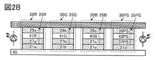
- 2A to 2D are cross-sectional views showing configuration examples of the display device.
- 3A and 3B are cross-sectional views showing configuration examples of the display device.
- FIG. 4A is a top view showing a configuration example of a display device.
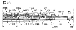
- FIG. 4B is a cross-sectional view showing a configuration example of the display device.
- 5A and 5B are cross-sectional views showing configuration examples of the display device.
- 6A to 6C are cross-sectional views showing configuration examples of the display device.
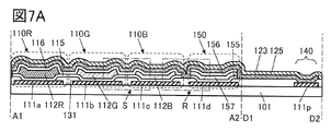
- 7A to 7C are cross-sectional views showing configuration examples of the display device.
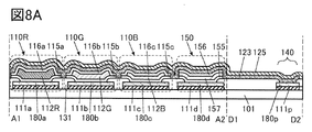
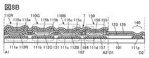
- 8A to 8C are cross-sectional views showing configuration examples of the display device.
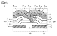
- 9A and 9B are cross-sectional views showing configuration examples of the display device.
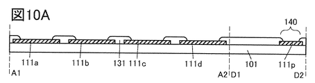
- 10A to 10E are cross-sectional views illustrating an example of a method for manufacturing a display device.
- 11A to 11D are cross-sectional views illustrating an example of a method for manufacturing a display device.
- 12A to 12D are cross-sectional views illustrating an example of a method for manufacturing a display device.
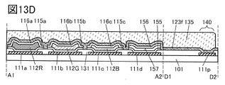
- 13A to 13D are cross-sectional views illustrating an example of a method for manufacturing a display device.
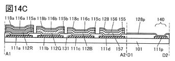
- 14A to 14C are cross-sectional views illustrating an example of a method for manufacturing a display device.
- 15A to 15D are cross-sectional views illustrating an example of a method for manufacturing a display device.
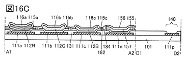
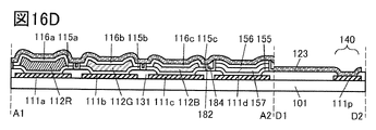
- 16A to 16D are cross-sectional views illustrating an example of a method for manufacturing a display device.
- 17A to 17D are cross-sectional views illustrating an example of a method for manufacturing a display device.
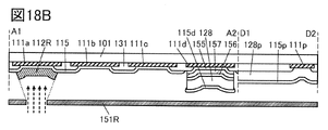
- 18A to 18D are cross-sectional views illustrating an example of a method for manufacturing a display device.
- 19A and 19B are cross-sectional views illustrating an example of a method for manufacturing a display device.
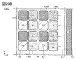
- 20A and 20B are top views showing configuration examples of the display device.
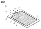
- FIG. 21 is a perspective view showing a configuration example of a display device.
- FIG. 22 is a cross-sectional view showing a configuration example of a display device.
- FIG. 23 is a cross-sectional view showing a configuration example of a display device.
- FIG. 21 is a perspective view showing a configuration example of a display device.
- FIG. 22 is a cross-sectional view showing a configuration example of a display device.
- FIG. 23 is a cross-sectional
- FIG. 24 is a cross-sectional view showing a configuration example of a display device.
- FIG. 25 is a cross-sectional view showing a configuration example of a display device.
- FIG. 26 is a cross-sectional view showing a configuration example of a display device.
- 27A to 27D are cross-sectional views showing configuration examples of light-emitting devices.
- 28A to 28G are cross-sectional views showing configuration examples of light receiving and emitting devices.
- 29A to 29E are diagrams illustrating examples of electronic devices.
- film and “layer” can be used interchangeably.
- conductive layer or “insulating layer” may be interchangeable with the terms “conductive film” or “insulating film.”
- an EL layer indicates a layer provided between a pair of electrodes of a light-emitting device and containing at least a light-emitting substance (also referred to as a light-emitting layer), or a laminate including a light-emitting layer.
- a display panel which is one aspect of a display device, has a function of displaying (outputting) an image or the like on a display surface. Therefore, the display panel is one aspect of the output device.
- the substrate of the display panel is attached with a connector such as FPC (Flexible Printed Circuit) or TCP (Tape Carrier Package), or an IC is mounted on the substrate by the COG (Chip On Glass) method, etc.
- a connector such as FPC (Flexible Printed Circuit) or TCP (Tape Carrier Package)
- COG Chip On Glass
- a display panel module a display module, or simply a display panel or the like.
- a display device of one embodiment of the present invention includes a display portion, and the display portion includes a plurality of pixels arranged in a matrix.
- a pixel has a light-emitting device and a light-receiving device (also referred to as a light-receiving element).
- a light-emitting device functions as a display device (also referred to as a display element).
- light-emitting devices are arranged in a matrix in a display portion, and an image can be displayed on the display portion. Further, the display device of one embodiment of the present invention has a function of detecting light using a light receiving device.
- light-receiving devices are arranged in a matrix, and the display portion has one or both of an imaging function and a sensing function in addition to an image display function.
- the display part can be used for an image sensor or a touch sensor. That is, by detecting light on the display portion, an image can be captured, or proximity or contact of an object (a finger, hand, pen, or the like) can be detected.
- the display device of one embodiment of the present invention can use a light-emitting device as a light source of a sensor. Therefore, it is not necessary to provide a light receiving portion and a light source separately from the display device, and the number of parts of the electronic device can be reduced.
- the display device can capture an image using the light receiving device.
- the display device of this embodiment can be used as a scanner.
- an image sensor can be used to acquire data related to biometric information such as fingerprints and palm prints. That is, the biometric authentication sensor can be incorporated in the display device.
- the biometric authentication sensor can be incorporated into the display device.
- the number of parts of the electronic device can be reduced compared to the case where the biometric authentication sensor is provided separately from the display device, and the electronic device can be small and lightweight. .
- the display device can detect proximity or contact of an object using the light receiving device.
- a device manufactured using a metal mask or FMM may be referred to as a device with an MM (metal mask) structure.
- a device manufactured without using a metal mask or FMM may be referred to as a device with an MML (metal maskless) structure.
- ⁇ Configuration example 1> 1A to 1D are cross-sectional views illustrating structural examples of display devices of one embodiment of the present invention.
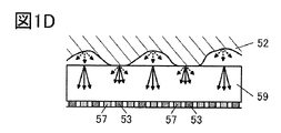
- the display device 100 shown in FIG. 1A has a layer 53 having light receiving devices and a layer 57 having light emitting devices between substrates 50 and 59 .
- FIG. 1A shows a configuration in which red (R), green (G), and blue (B) lights are emitted from a layer 57 having light-emitting devices, and light is incident on a layer 53 having light-receiving devices.
- R red
- G green
- B blue
- FIG. 1A light emitted from the layer 57 and light incident on the layer 53 are indicated by arrows.
- the wavelength region of blue (B) is 400 nm or more and less than 490 nm, and blue (B) light has at least one emission spectrum peak in this wavelength region.
- the wavelength region of green (G) is 490 nm or more and less than 580 nm, and green (G) light has at least one emission spectrum peak in this wavelength region.
- the wavelength region of red (R) is 580 nm or more and less than 700 nm, and red (R) light has at least one emission spectrum peak in this wavelength region.
- the wavelength region of visible light is from 400 nm to less than 700 nm, and visible light has at least one emission spectrum peak in this wavelength region.
- the infrared (IR) wavelength range is from 700 nm to less than 900 nm, and the infrared (IR) light has at least one emission spectrum peak in this wavelength range.
- a display device of one embodiment of the present invention includes a plurality of pixels arranged in a matrix in a display portion.
- One pixel has one or more sub-pixels.
- Each subpixel has a light emitting device or a light receiving device.
- a pixel can have four sub-pixels.
- one pixel includes a sub-pixel having a light-emitting device that emits red (R) light, a sub-pixel having a light-emitting device that emits green (G) light, and a sub-pixel having a light-emitting device that emits blue (B) light. and a sub-pixel having a light-receiving device.
- the combination of colors of light emitted by the light emitting device included in the pixel is not limited to red (R), green (G), and blue (B).
- the combination of colors of light emitted by the light emitting device of the pixel can be, for example, yellow (Y), cyan (C), and magenta (M). Note that four or more colors of light emitted by the light-emitting device included in the pixel may be used.
- a pixel may be configured to have five or more sub-pixels. Specifically, one pixel can be configured to have four types of light-emitting devices of red (R), green (G), blue (B), and white (W) and a light-receiving device. . Further, it is possible to adopt a configuration having four kinds of light emitting devices of red (R), green (G), blue (B), and infrared (IR) and a light receiving device. Note that the light receiving device may be provided in all the pixels, or may be provided in some of the pixels. Note that one pixel may have a plurality of light receiving devices. For example, one pixel may include three light emitting devices of red (R), green (G), and blue (B), a light receiving device sensitive to the visible wavelength range, and an infrared wavelength range. and a light receiving device having sensitivity.
- a display device of one embodiment of the present invention can have a function of detecting an object in contact with the display device.
- the object is not particularly limited, and can be a living body or an object.
- the display device can have a function of detecting a finger or palm, for example.
- FIG. 1B light emitted by a light-emitting device in layer 57 is reflected by finger 52 touching display device 100, and a light-receiving device in layer 53 detects the reflected light. Thereby, it is possible to detect that the finger 52 touches the display device 100 .
- the display device of one embodiment of the present invention can function as a touch sensor. Further, as shown in FIG.
- the display device of one embodiment of the present invention can function as a near-touch sensor.
- the display device 100 has a function as a near-touch sensor, even if the finger 52 does not touch the display device 100, the finger 52 can be detected by approaching the display device 100. It is preferable that the display device 100 can detect the finger 52 when the distance between the display device 100 and the finger 52 is, for example, 0.1 mm or more and 300 mm or less, preferably 3 mm or more and 50 mm or less. With this configuration, it is possible to operate the display device 100 without directly touching the finger 52 , in other words, it is possible to operate the display device 100 in a non-contact (touchless) manner. With the above structure, the risk of staining or scratching the display device 100 can be reduced, or the finger 52 can directly touch stains (for example, dust or viruses) that may adhere to the display device 100. It is possible to operate the display device 100 without having to
- a display device of one embodiment of the present invention can have a function of imaging an object that is in contact with the display device.
- the display device may have the ability to detect the fingerprint of finger 52, for example.
- FIG. 1D schematically shows an enlarged view of the contact portion when the finger 52 is in contact with the substrate 59.
- FIG. 1D also shows that layers 57 having light-emitting devices and layers 53 having light-receiving devices are alternately arranged.
- a fingerprint is formed on the finger 52 by concave portions and convex portions. Therefore, the raised portion of the fingerprint touches the substrate 59 as shown in FIG. 1D.
- Specularly reflected light is highly directional light whose incident angle and reflected angle are the same, and diffusely reflected light is light with low angle dependence of intensity and low directivity.
- the light reflected from the surface of the finger 52 is dominated by the diffuse reflection component of the specular reflection and the diffuse reflection.
- the light reflected from the interface between the substrate 59 and the atmosphere is predominantly a specular reflection component.
- the intensity of the light reflected by the contact surface or the non-contact surface between the finger 52 and the substrate 59 and incident on the layer 53 located directly below them is the sum of specularly reflected light and diffusely reflected light.
- the specularly reflected light (indicated by the solid line arrow) is dominant. indicated by dashed arrows) becomes dominant. Therefore, the intensity of light received by the light-receiving device of the layer 53 located directly below the recess is higher than the intensity of light received by the light-receiving device of the layer 53 located directly below the protrusion. Therefore, the fingerprint of the finger 52 can be imaged using the light receiving device.
- the arrangement interval of the light-receiving devices included in the layer 53 is set to be smaller than the distance between two protrusions of the fingerprint, preferably smaller than the distance between adjacent recesses and protrusions, so that a clear fingerprint image can be obtained. can be done. Since the distance between concave and convex portions of a human fingerprint is approximately 150 ⁇ m to 250 ⁇ m, the array interval of light receiving devices is, for example, 400 ⁇ m or less, preferably 200 ⁇ m or less, more preferably 150 ⁇ m or less, and even more preferably 120 ⁇ m or less. , more preferably 100 ⁇ m or less, more preferably 50 ⁇ m or less. Although the arrangement interval is preferably as small as possible, it can be, for example, 1 ⁇ m or more, 10 ⁇ m or more, or 20 ⁇ m or more.
- FIG. 1E is an example of a fingerprint image captured by the display device of one embodiment of the present invention.
- the outline of the finger 52 is indicated by a dashed line
- the outline of the contact portion 69 is indicated by a dashed line.
- a high-contrast fingerprint 67 can be imaged due to the difference in the amount of light incident on the light-receiving device.
- fingerprint authentication can be performed using the obtained fingerprint image.
- the display device can detect a palm in contact with or in close proximity to the display.
- the display device can capture an image of a palmprint, and can perform palmprint authentication using the acquired palmprint image.
- the light-receiving device can detect light emitted by the light-emitting device, applied to the object, and reflected by the object. Therefore, even in a dark place, it is possible to detect an object that is in contact with or close to the display unit. Furthermore, the display device can perform authentication such as fingerprint authentication and palm print authentication.
- the display device By providing the light receiving device in the display unit, there is no need to externally attach the sensor to the display device. Therefore, since the number of parts can be reduced, the display device can be small and lightweight.
- a substrate having heat resistance that can withstand the formation of light emitting devices and light receiving devices can be used.
- a glass substrate, a quartz substrate, a sapphire substrate, a ceramic substrate, an organic resin substrate, or the like can be used.
- a semiconductor substrate such as a single crystal semiconductor substrate, a polycrystalline semiconductor substrate, a compound semiconductor substrate made of silicon germanium or the like, or an SOI substrate can be used.
- the substrate 50 it is preferable to use a substrate in which a semiconductor circuit including a semiconductor element such as a transistor is formed on the insulating substrate or semiconductor substrate described above.
- the semiconductor circuit preferably constitutes, for example, a pixel circuit, a gate line driver circuit (gate driver), a source line driver circuit (source driver), and the like.
- gate driver gate line driver
- source driver source driver
- an arithmetic circuit, a memory circuit, and the like may be configured.
- FIG. 2A shows configurations of a light-emitting device 20R, a light-emitting device 20G, a light-emitting device 20B, and a light-receiving device 30PS that can be applied to a display device.
- the light-emitting device 20R, the light-emitting device 20G, and the light-emitting device 20B each have a function of emitting light (hereinafter also referred to as a light-emitting function).
- the light-emitting device 20R, the light-emitting device 20G, and the light-emitting device 20B preferably use EL elements such as OLEDs (Organic Light Emitting Diodes) or QLEDs (Quantum-dot Light Emitting Diodes).
- Examples of light-emitting substances in EL devices include substances that emit fluorescence (fluorescent materials), substances that emit phosphorescence (phosphorescent materials), inorganic compounds (quantum dot materials, etc.), and substances that exhibit heat-activated delayed fluorescence (heat-activated delayed fluorescence (TADF: Thermally Activated Delayed Fluorescence) material) and the like.
- TADF heat-activated delayed fluorescence
- As the TADF material a material in which the singlet excited state and the triplet excited state are in thermal equilibrium may be used. Since such a TADF material has a short emission lifetime (excitation lifetime), it is possible to suppress a decrease in efficiency in a high-luminance region of a light-emitting device.
- the light-emitting device 20R has an electrode 21a, an EL layer 25R, and an electrode 23.
- the light emitting device 20G has an electrode 21b, an EL layer 25G, and an electrode 23.
- the light-emitting device 20B has an electrode 21c, an EL layer 25B, and an electrode 23.
- FIG. In the light-emitting device 20R the EL layer 25R sandwiched between the electrodes 21a and 23 has at least the light-emitting layer 41R.
- the light-emitting layer 41R has a light-emitting material that emits light. By applying a voltage between the electrode 21a and the electrode 23, light is emitted from the EL layer 25R.
- the EL layer 25G has at least a light emitting layer 41G.
- the light-emitting layer 41G has a light-emitting material that emits light.
- the EL layer 25B has at least a light emitting layer 41B.
- the light-emitting layer 41B has a light-emitting material that emits light.
- Each of the EL layer 25R, the EL layer 25G, and the EL layer 25B further includes a layer containing a highly hole-injecting substance (hereinafter referred to as a hole-injecting layer) and a layer containing a highly hole-transporting substance (hereinafter referred to as a hole-transporting substance).
- a hole transport layer a layer containing a highly electron-transporting substance (hereinafter referred to as an electron-transporting layer), a layer containing a highly electron-injecting substance (hereinafter referred to as an electron-injecting layer), a carrier block layer , an exciton blocking layer, and a charge generating layer.
- the hole injection layer, hole transport layer, electron transport layer, electron injection layer, carrier block layer, exciton block layer, and charge generation layer can also be called functional layers.
- the light emitting device 20 when describing matters common to the light emitting device 20R, the light emitting device 20G, and the light emitting device 20B, or when there is no need to distinguish them, the light emitting device 20 may be simply referred to.
- the EL layer 25R, the EL layer 25G, and the EL layer 25B may be simply referred to as the EL layer 25 in some cases. The same applies to other constituent elements.
- the light receiving device 30PS has a function of detecting light (hereinafter also referred to as a light receiving function).
- the light receiving device 30PS has a function of detecting visible light.
- the light receiving device 30PS is sensitive to visible light. More preferably, the light receiving device 30PS has a function of detecting visible light and infrared light.
- the light receiving device 30PS is preferably sensitive to visible light and infrared light.
- a pn-type or pin-type photodiode can be used.
- the light receiving device 30PS has an electrode 21d, a light receiving layer 35PS, and an electrode 23.
- the light receiving layer 35PS sandwiched between the electrode 21d and the electrode 23 has at least an active layer.
- the light-receiving device 30PS functions as a photoelectric conversion device, and can generate electric charge by light incident on the light-receiving layer 35PS and extract it as a current. At this time, a voltage may be applied between the electrode 21d and the electrode 23.
- FIG. The amount of charge generated is determined based on the amount of light incident on the light receiving layer 35PS.
- the light-receiving layer 35PS may further include one or more of a hole-transporting layer, an electron-transporting layer, a layer containing a bipolar substance (a substance with high electron-transporting and hole-transporting properties), and a carrier block layer. good.
- the light receiving layer 35PS may have a layer containing a substance that can be used as a hole injection layer. In the light receiving device 30PS, this layer can function as a hole transport layer. Also, the light receiving layer 35PS may have a layer containing a substance that can be used as an electron injection layer. In the light receiving device 30PS, this layer can function as an electron transport layer. Note that a substance having a hole-injecting property can also be said to have a hole-transporting property.
- a substance having an electron-injecting property can also be said to have an electron-transporting property. Therefore, in this specification and the like, a substance having a hole-injecting property is sometimes referred to as a substance having a hole-transporting property. Similarly, an electron-injecting substance is sometimes referred to as an electron-transporting substance.
- the active layer contains a semiconductor.
- the semiconductor include inorganic semiconductors such as silicon and organic semiconductors including organic compounds.
- organic photodiode having a layer containing an organic semiconductor as the light receiving device 30PS.
- Organic photodiodes can be easily made thinner, lighter, and larger, and have a high degree of freedom in shape and design, so that they can be applied to various display devices.
- the EL layer of the light emitting device 20 and the light receiving layer of the light receiving device 30PS can be formed by the same method (eg, vacuum deposition method), and a common manufacturing apparatus can be used. It is preferable because it can be done.
- the display device of one embodiment of the present invention can suitably use organic EL devices as the light-emitting devices 20R, 20G, and 20B, and organic photodiodes as the light-receiving devices 30PS.
- An organic EL device and an organic photodiode can be formed on the same substrate. Therefore, an organic photodiode can be incorporated in a display device using an organic EL device.
- a display device which is one embodiment of the present invention has one or both of an imaging function and a sensing function in addition to a function of displaying an image.
- FIG. 2A shows a configuration in which electrode 21a, electrode 21b, electrode 21c, and electrode 21d are provided on substrate 50.
- FIG. 2A shows a configuration in which electrode 21a, electrode 21b, electrode 21c, and electrode 21d are provided on substrate 50.
- FIG. The same material can be used for the electrodes 21a, 21b, 21c, and 21d.
- the electrode 21a, the electrode 21b, the electrode 21c, and the electrode 21d can be formed through the same process.
- the electrodes 21a, 21b, 21c, and 21d can be formed by processing a conductive film formed on the substrate 50 into an island shape.
- the electrodes 21a, 21b, 21c, and 21d can be called pixel electrodes.
- the electrode 23 is a layer common to the light emitting device 20R, the light emitting device 20G, the light emitting device 20B, and the light receiving device 30PS, and can be called a common electrode.
- a conductive film that transmits visible light and infrared light is used for the electrode on the side from which light is emitted or from which light is incident, of the pixel electrode and the common electrode.
- a conductive film that reflects visible light and infrared light is preferably used for the electrode on the side from which light is not emitted or incident.
- FIG. 2A shows a configuration in which the electrodes 21a, 21b, 21c, and 21d function as anodes and the electrodes 23 function as cathodes in each of the light-emitting device 20R, the light-emitting device 20G, the light-emitting device 20B, and the light-receiving device 30PS. is schematically shown.
- the circuit symbol of the light-emitting diode is shown on the left side of the light-emitting device 20R
- the circuit symbol of the photodiode is shown on the right side of the light-receiving device 30PS, in order to make the orientation of the anode and cathode easier to understand.
- electrons are indicated by circles with - (minus)
- holes are indicated by circles with + (plus)
- directions of flow of electrons and holes are schematically indicated by arrows.
- the electrodes 21a, 21b, and 21c functioning as anodes are electrically connected to the first wiring that supplies the first potential.
- the electrode 23 functioning as a cathode is electrically connected to the second wiring that supplies the second potential.
- the second potential is lower than the first potential.
- the electrode 21d functioning as an anode is electrically connected to a third wiring that supplies a third potential.
- a reverse bias voltage is applied to the light receiving device 30PS. That is, the third potential is lower than the second potential.
- FIG. 2B A specific example of the configuration shown in FIG. 2A is shown in FIG. 2B.
- the EL layer 25R has a first layer 27a, a light-emitting layer 41R, and a second layer 29a laminated in this order.
- the EL layer 25G has a first layer 27b, a light-emitting layer 41G, and a second layer 29b laminated in this order.
- the EL layer 25B has a first layer 27c, a light-emitting layer 41B, and a second layer 29c laminated in this order.
- the structure having the first layer 27a, the light-emitting layer 41R, and the second layer 29a provided between a pair of electrodes (electrode 21a and electrode 23) functions as a single light-emitting unit.
- the configuration of the light emitting device 20R may be referred to as a single configuration. The same applies to the light emitting device 20G and the light emitting device 20B.
- the first layer 27a, the first layer 27b, and the first layer 27c are positioned on the side of the electrodes 21a, 21b, and 21c functioning as anodes in the light-emitting device 20R, the light-emitting device 20G, and the light-emitting device 20B. do.
- Each of the first layer 27a, the first layer 27b, and the first layer 27c can be a hole transport layer or a hole injection layer.
- each of the first layer 27a, the first layer 27b, and the first layer 27c may have a laminated structure of a hole injection layer and a hole transport layer on the hole injection layer.
- the hole injection layer may have a laminated structure
- the hole transport layer may have a laminated structure.
- the first layer 27a, the first layer 27b, and the first layer 27c may each contain a substance having a hole-transporting property and a substance having a hole-injecting property.
- the first layer 27a, the first layer 27b, and the first layer 27c may be referred to as functional layers.
- the same material can be used for the first layer 27a, the first layer 27b, and the first layer 27c.
- the first layer 27a, the first layer 27b, and the first layer 27c can be formed through the same process.
- the first layer 27a, the first layer 27b, and the first layer 27c can be formed by processing the films that become the first layer 27a, the first layer 27b, and the first layer 27c. .
- the productivity of the display device can be improved.
- the second layer 29a, the second layer 29b, and the second layer 29c are located on the side of the electrode 23 functioning as a cathode in the light emitting device 20R, the light emitting device 20G, and the light emitting device 20B.
- Second layer 29a, second layer 29b, and second layer 29c can each be an electron transport layer or an electron injection layer.
- each of the second layer 29a, the second layer 29b, and the second layer 29c may have a laminated structure of an electron transport layer and an electron injection layer on the electron transport layer.
- the electron injection layer may have a laminated structure
- the electron transport layer may have a laminated structure.
- the second layer 29a, the second layer 29b, and the second layer 29c may each contain an electron-transporting substance and an electron-injecting substance.
- the second layer 29a, the second layer 29b, and the second layer 29c may be referred to as functional layers.
- the same material can be used for the second layer 29a, the second layer 29b, and the second layer 29c.
- the second layer 29a, the second layer 29b, and the second layer 29c can be formed through the same process.
- the second layer 29a, the second layer 29b, and the second layer 29c can be formed by processing the films that become the second layer 29a, the second layer 29b, and the second layer 29c. .
- the productivity of the display device can be improved.
- the light receiving layer 35PS has a third layer 37PS, an active layer 43PS, and a fourth layer 39PS laminated in this order.
- the third layer 37PS located on the side of the electrode 21d functioning as the anode of the light receiving device 30PS can be a hole transport layer.
- the hole-transporting substance contained in the third layer 37PS may be different from the hole-transporting substance contained in the first layer 27a, the first layer 27b, and the first layer 27c.
- the third layer 37PS of the light-receiving device 30PS is preferably formed in a process different from the layers forming the light-emitting device 20 (eg, the first layer 27a, the first layer 27b, and the first layer 27c). . By forming in a different process, a material more suitable for the light receiving device 30PS can be applied to the third layer 37PS. In this specification and the like, the third layer 37PS may be referred to as a functional layer.
- the material that can be used for the first layer 27a, the first layer 27b, and the first layer 27c can be used for the third layer 37PS.
- the hole-transporting substance contained in the third layer 37PS may be the same as the hole-transporting substance contained in the first layer 27a, the first layer 27b, and the first layer 27c. .
- the third layer 37PS may have a laminated structure.
- the fourth layer 39PS located on the electrode 23 side that functions as the cathode of the light receiving device 30PS can be an electron transport layer.
- the electron-transporting substance contained in the fourth layer 39PS may be different from the electron-transporting substance contained in the second layers 29a, 29b, and 29c.
- the fourth layer 39PS of the light-receiving device 30PS is preferably formed in a process different from the layers forming the light-emitting device 20 (for example, the second layer 29a, the second layer 29b, and the second layer 29c). . By forming in a different process, a material more suitable for the light receiving device 30PS can be applied to the fourth layer 39PS. In this specification and the like, the fourth layer 39PS may be referred to as a functional layer.
- the fourth layer 39PS can use the material that can be used for the second layer 29a, the second layer 29b, and the second layer 29c.
- the electron-transporting substance contained in the fourth layer 39PS may be the same as the electron-transporting substance contained in the second layers 29a, 29b, and 29c.
- the fourth layer 39PS may have a laminated structure.
- the third layer 37PS may have a layer that functions as a hole injection layer in the light emitting device, that is, a layer containing a substance with high hole injection properties.
- a hole-injecting layer can function as a hole-transporting layer in a light-receiving device.
- the fourth layer 39PS may have a layer that functions as an electron injection layer in the light emitting device, ie a layer containing a substance with high electron injection properties.
- An electron-injecting layer can function as an electron-transporting layer in a light-receiving device.
- the EL layer 25R, the EL layer 25G, the EL layer 25B, and the light receiving layer 35PS do not have layers in common with each other. Moreover, it is preferable that the EL layer 25R, the EL layer 25G, the EL layer 25B, and the light-receiving layer 35PS do not have regions in contact with each other. That is, it is preferable that the EL layer 25R, the EL layer 25G, the EL layer 25B, and the light receiving layer 35PS are separated.
- the light-receiving layer 35PS of the light-receiving device 30PS is separated from the EL layer 25 of the adjacent light-emitting device 20, so that leakage current (also referred to as side leak) flowing from the light-emitting device 20 to the light-receiving device 30PS can be suppressed. Therefore, the light-receiving device 30PS can have a high SN ratio (Signal to Noise Ratio) and high accuracy.
- the distance between the light emitting device 20 and the light receiving device 30PS can be narrowed.
- the ratio of the light emitting device 20 and the light receiving device 30PS to the pixels (hereinafter also referred to as aperture ratio) can be increased.
- the pixel size can be reduced, and the definition of the display device can be improved. Therefore, a display device having a photodetection function and a high aperture ratio can be realized. Further, a high-definition display device having a photodetection function can be realized.
- the resolution of the light receiving device 30PS should be 100 ppi or more, preferably 200 ppi or more, more preferably 300 ppi or more, more preferably 400 ppi or more, still more preferably 500 ppi or more, and 2000 ppi or less, 1000 ppi or less, or 600 ppi or less. can be done. In particular, by setting the resolution of the light receiving device 30PS to 200 ppi or more and 600 ppi or less, preferably 300 ppi or more and 600 ppi or less, it can be suitably used for fingerprint imaging.
- the resolution of the light-receiving device 30PS is 500 ppi or more, it is preferable because it can conform to standards such as the US National Institute of Standards and Technology (NIST). Assuming that the resolution of the light-receiving device is 500 ppi, the size of one pixel is 50.8 ⁇ m, which is sufficient resolution to capture the width of a fingerprint (typically, 300 ⁇ m or more and 500 ⁇ m or less). I understand.
- FIG. 2C A configuration different from that shown in FIGS. 2A and 2B is shown in FIG. 2C.
- the electrodes 21a, 21b, and 21c function as anodes
- the electrode 23 functions as a cathode
- the light-receiving device 30PS It schematically shows a configuration in which the electrode 21d functions as a cathode and the electrode 23 functions as an anode.
- the electrodes 21a, 21b, and 21c functioning as anodes are electrically connected to the first wiring that supplies the first potential.
- An electrode 23 that functions as a cathode in the light-emitting device 20R, the light-emitting device 20G, and the light-emitting device 20B and functions as an anode in the light-receiving device 30PS is electrically connected to a second wiring that supplies a second potential. be. The second potential is lower than the first potential.
- the electrode 21d functioning as a cathode is electrically connected to a third wiring that supplies a third potential. The third potential is a potential higher than the second potential.
- the electrode 23 functioning as a common electrode functions as either an anode or a cathode in the light-emitting device 20R, the light-emitting device 20G, and the light-emitting device 20B, and functions as the other anode or cathode in the light-receiving device 30PS.
- the potential difference between the pixel electrodes (electrodes 21a, 21b and 21c) of the light emitting device 20 and the pixel electrode (electrode 21d) of the light receiving device 30PS can be reduced. Leakage (hereinafter also referred to as side leak) can be suppressed. Therefore, the light-receiving device 30PS can have a high SN ratio and a high accuracy.
- the first potential (the potential supplied to the electrodes 21a, 21b, and 21c) is 12 V
- the second potential (the potential supplied to the electrode 23) is 0 V
- the third potential (the potential supplied to the electrode 21d) is 12 V. potential) can be 4V.
- the potential difference between the pixel electrodes (electrodes 21a, 21b and 21c) of the light emitting device 20 and the pixel electrode (electrode 21d) of the light receiving device 30PS can be reduced. A side leak with the device 30PS can be suppressed.
- the display device can consume less power.
- FIG. 2D A specific example of the configuration shown in FIG. 2C is shown in FIG. 2D.
- the above description can be referred to, so detailed description thereof will be omitted.
- the third layer 37PS located on the side of the electrode 21d functioning as the cathode of the light receiving device 30PS can be an electron transport layer.
- the electron-transporting substance contained in the third layer 37PS may be different from the electron-transporting substance contained in the second layers 29a, 29b, and 29c.
- the third layer 37PS can use the material that can be used for the second layer 29a, the second layer 29b, and the second layer 29c.
- the electron-transporting substance contained in the third layer 37PS may be the same as the electron-transporting substance contained in the second layers 29a, 29b, and 29c.
- the fourth layer 39PS located on the electrode 23 side that functions as the anode of the light receiving device 30PS can be a hole transport layer.
- the hole-transporting substance contained in the fourth layer 39PS may be different from the hole-transporting substance contained in the first layer 27a, the first layer 27b, and the first layer 27c.
- a material that can be used for the first layer 27a, the first layer 27b, and the first layer 27c can be used.
- the hole-transporting substance contained in the fourth layer 39PS may be the same as the hole-transporting substance contained in the first layer 27a, the first layer 27b, and the first layer 27c. .
- the third layer 37PS may have a layer that functions as an electron injection layer in the light emitting device, that is, a layer containing a substance with high electron injection properties.
- the fourth layer 39PS may comprise a layer that functions as a hole injection layer in a light emitting device, ie a layer containing a substance with high hole injection properties.
- the electrodes 21a, 21b, and 21c function as anodes and the electrode 23 functions as a cathode in the light-emitting device 20
- the electrodes 21a, 21b, and 21c may function as cathodes
- the electrode 23 may function as an anode.
- the first layer 27a, the first layer 27b, and the first layer 27c can be one or both of an electron-transporting layer and an electron-injecting layer.
- Second layer 29a, second layer 29b, and second layer 29c can be one or both of a hole transport layer or a hole injection layer.
- FIG. 3A A configuration different from that shown in FIG. 2B is shown in FIG. 3A.
- Light emitting device 20R, light emitting device 20G, and light emitting device 20B shown in FIG. 3A have first layer 27 instead of first layer 27a, first layer 27b, and first layer 27c, and a second It has a second layer 29 instead of the layer 29a, the second layer 29b, and the second layer 29c.
- the first layer 27 is a layer common to the light emitting device 20R, the light emitting device 20G, and the light emitting device 20B, and can be called a first common layer.
- second layer 29 is a layer common to light emitting device 20R, light emitting device 20G, and light emitting device 20B and can be referred to as a second common layer.
- the first layer 27 located on the side of the electrodes 21a, 21b, and 21c functioning as anodes of the light-emitting device 20R, the light-emitting device 20G, and the light-emitting device 20B is a hole transport layer or a positive electrode. It can be a hole injection layer. Alternatively, the first layer 27 may have a laminate structure of a hole injection layer and a hole transport layer on the hole injection layer. For the first layer 27, the description of the first layer 27a, the first layer 27b, and the first layer 27c can be referred to, so detailed description thereof is omitted.
- the second layer 29 located on the side of the electrode 23 that functions as the cathode of the light emitting device 20R, the light emitting device 20G, and the light emitting device 20B can be an electron transport layer or an electron injection layer.
- the second layer 29 may have a laminated structure of an electron transport layer and an electron injection layer on the electron transport layer.
- the description of the second layer 29a, the second layer 29b, and the second layer 29c can be referred to, so detailed description thereof is omitted.
- a third common layer may be provided between the electrode 23 and the second layer 29 and between the electrode 23 and the fourth layer 39PS.
- the third common layer has, for example, an electron injection layer.
- the third common layer may have a laminate structure of an electron transport layer and an electron injection layer on the electron transport layer.
- a third common layer is a layer common to the light emitting device 20R, the light emitting device 20G, the light emitting device 20B, and the light receiving device 30PS. Note that when an electron injection layer is used for the third common layer, the electron injection layer functions as an electron transport layer in the light receiving device 30PS.
- the light receiving device 30PS may have a configuration in which the electrode 21d functions as a cathode and the electrode 23 functions as an anode.
- a third common layer may be provided between the electrode 23 and the second layer 29 and between the electrode 23 and the fourth layer 39PS.
- the above description can be referred to, so a detailed description is omitted. Note that when an electron injection layer is used for the third common layer, the electron injection layer does not have to have a specific function in the light receiving device 30PS.
- the hole-injecting layer is a layer that injects holes from the anode into the hole-transporting layer, and contains a material with high hole-injecting properties.
- highly hole-injecting materials include aromatic amine compounds and composite materials containing a hole-transporting material and an acceptor material (electron-accepting material).
- a hole-transporting layer is a layer that transports holes injected from the anode to the light-emitting layer by means of a hole-injecting layer.
- the hole-transporting layer is a layer that transports holes generated by incident light in the active layer to the anode.
- a hole-transporting layer is a layer containing a hole-transporting material.
- the hole-transporting material is preferably a substance having a hole mobility of 10 ⁇ 6 cm 2 /Vs or more. Note that substances other than these can be used as long as they have a higher hole-transport property than electron-transport property.
- the hole-transporting materials include materials with high hole-transporting properties such as ⁇ -electron-rich heteroaromatic compounds (e.g., carbazole derivatives, thiophene derivatives, furan derivatives, etc.) and aromatic amines (compounds having an aromatic amine skeleton). preferable.
- ⁇ -electron-rich heteroaromatic compounds e.g., carbazole derivatives, thiophene derivatives, furan derivatives, etc.
- aromatic amines compounds having an aromatic amine skeleton.
- an electron-transporting layer is a layer that transports electrons injected from the cathode to the light-emitting layer by the electron-injecting layer.
- the electron transport layer is a layer that transports electrons generated by incident light in the active layer to the cathode.
- the electron-transporting layer is a layer containing an electron-transporting material.
- the electron-transporting material is preferably a substance having an electron mobility of 1 ⁇ 10 ⁇ 6 cm 2 /Vs or more. Note that substances other than these substances can be used as long as they have a higher electron-transport property than hole-transport property.
- Electron-transporting materials include metal complexes having a quinoline skeleton, metal complexes having a benzoquinoline skeleton, metal complexes having an oxazole skeleton, metal complexes having a thiazole skeleton, oxadiazole derivatives, triazole derivatives, imidazole derivatives, and oxazole. derivatives, thiazole derivatives, phenanthroline derivatives, quinoline derivatives with quinoline ligands, benzoquinoline derivatives, quinoxaline derivatives, dibenzoquinoxaline derivatives, pyridine derivatives, bipyridine derivatives, pyrimidine derivatives, and other nitrogen-containing heteroaromatic compounds.
- a material having a high electron-transport property such as a heteroaromatic compound can be used.
- the electron injection layer is a layer that injects electrons from the cathode to the electron transport layer, and is a layer that contains a material with high electron injection properties.
- Alkali metals, alkaline earth metals, or compounds thereof can be used as materials with high electron injection properties.
- a composite material containing an electron-transporting material and a donor material (electron-donating material) can also be used as a material with high electron-injecting properties.
- the electron injection layer includes, for example, lithium, cesium, ytterbium, lithium fluoride (LiF), cesium fluoride (CsF), calcium fluoride (CaF 2 ), 8-(quinolinolato)lithium (abbreviation: Liq), 2-( 2-pyridyl)phenoratritium (abbreviation: LiPP), 2-(2-pyridyl)-3-pyridinolatritium (abbreviation: LiPPy), 4-phenyl-2-(2-pyridyl)phenoratritium (abbreviation: LiPPP) ), lithium oxide (LiO x ), alkali metals such as cesium carbonate, alkaline earth metals, or compounds thereof.
- the electron injection layer may have a laminated structure of two or more layers. As the laminated structure, for example, lithium fluoride can be used for the first layer and ytterbium can be used for the second layer.
- an electron-transporting material may be used for the electron injection layer.
- a compound having a lone pair of electrons and an electron-deficient heteroaromatic ring can be used as the electron-transporting material.
- a compound having at least one of a pyridine ring, diazine ring (pyrimidine ring, pyrazine ring, pyridazine ring), and triazine ring can be used.
- the lowest unoccupied molecular orbital (LUMO) of the organic compound having an unshared electron pair is preferably -3.6 eV or more and -2.3 eV or less.
- CV cyclic voltammetry
- photoelectron spectroscopy optical absorption spectroscopy
- inverse photoelectron spectroscopy etc. are used to determine the highest occupied molecular orbital (HOMO: Highest Occupied Molecular Orbital) level and LUMO level of an organic compound. can be estimated.
- BPhen 4,7-diphenyl-1,10-phenanthroline
- NBPhen 2,9-di(naphthalen-2-yl)-4,7-diphenyl-1,10-phenanthroline
- HATNA diquinoxalino [2,3-a:2′,3′-c]phenazine
- TmPPPyTz 2,4,6-tris[3′-(pyridin-3-yl)biphenyl-3-yl]-1,3 , 5-triazine
- charge generation layer materials applicable to the electron injection layer, such as lithium, can be suitably used.
- a material applicable to the hole injection layer can be suitably used.
- a layer containing a hole-transporting material and an acceptor material (electron-accepting material) can be used as the charge-generating layer.
- a layer containing an electron-transporting material and a donor material can be used for the charge generation layer.
- the active layer contains a semiconductor.
- the semiconductor include inorganic semiconductors such as silicon and organic semiconductors including organic compounds.
- an organic semiconductor is used as the semiconductor included in the active layer.
- the light-emitting layer and the active layer can be formed by the same method (for example, a vacuum deposition method), and a manufacturing apparatus can be shared, which is preferable.
- Electron-accepting organic semiconductor materials such as fullerenes (eg, C 60 , C 70 , etc.) and fullerene derivatives are examples of the n-type semiconductor material of the active layer.
- Fullerenes have a soccer ball-like shape, which is energetically stable.
- Fullerene has both deep (low) HOMO and LUMO levels. Since fullerene has a deep LUMO level, it has an extremely high electron-accepting property (acceptor property). Normally, as in benzene, if the ⁇ -electron conjugation (resonance) spreads in the plane, the electron-donating property (donor property) increases. and the electron acceptability becomes higher.
- a high electron-accepting property is useful as a light-receiving device because charge separation occurs quickly and efficiently.
- Both C 60 and C 70 have broad absorption bands in the visible light region, and C 70 is particularly preferable because it has a larger ⁇ -electron conjugated system than C 60 and has a wide absorption band in the long wavelength region.
- [6,6]-Phenyl-C71-butylic acid methyl ester (abbreviation: PC70BM), [6,6]-Phenyl-C61-butylic acid methyl ester (abbreviation: PC60BM), 1′,1 '',4',4''-Tetrahydro-di[1,4]methanonaphthaleno[1,2:2',3',56,60:2'',3''][5,6]fullerene-C60 (abbreviation: ICBA) and the like.
- PC70BM [6,6]-Phenyl-C71-butylic acid methyl ester
- PC60BM [6,6]-Phenyl-C61-butylic acid methyl ester
- ICBA 1,6]fullerene-C60
- n-type semiconductor materials include perylenetetracarboxylic acid derivatives such as N,N'-dimethyl-3,4,9,10-perylenetetracarboxylic acid diimide (abbreviation: Me-PTCDI).
- n-type semiconductor materials include 2,2′-(5,5′-(thieno[3,2-b]thiophene-2,5-diyl)bis(thiophene-5,2-diyl))bis( methane-1-yl-1-ylidene)dimalononitrile (abbreviation: FT2TDMN).
- n-type semiconductor materials include metal complexes having a quinoline skeleton, metal complexes having a benzoquinoline skeleton, metal complexes having an oxazole skeleton, metal complexes having a thiazole skeleton, oxadiazole derivatives, triazole derivatives, imidazole derivatives, oxazole derivatives, Thiazole derivatives, phenanthroline derivatives, quinoline derivatives, benzoquinoline derivatives, quinoxaline derivatives, dibenzoquinoxaline derivatives, pyridine derivatives, bipyridine derivatives, pyrimidine derivatives, naphthalene derivatives, anthracene derivatives, coumarin derivatives, rhodamine derivatives, triazine derivatives, quinone derivatives, etc. .
- Materials for the p-type semiconductor of the active layer include copper (II) phthalocyanine (CuPc), tetraphenyldibenzoperiflanthene (DBP), zinc phthalocyanine (ZnPc), tin phthalocyanine ( SnPc), quinacridone, rubrene, and other electron-donating organic semiconductor materials.
- CuPc copper
- DBP tetraphenyldibenzoperiflanthene
- ZnPc zinc phthalocyanine
- SnPc tin phthalocyanine
- quinacridone quinacridone
- rubrene and other electron-donating organic semiconductor materials.
- Examples of p-type semiconductor materials include carbazole derivatives, thiophene derivatives, furan derivatives, and compounds having an aromatic amine skeleton. Furthermore, materials for p-type semiconductors include naphthalene derivatives, anthracene derivatives, pyrene derivatives, triphenylene derivatives, fluorene derivatives, pyrrole derivatives, benzofuran derivatives, benzothiophene derivatives, indole derivatives, dibenzofuran derivatives, dibenzothiophene derivatives, indolocarbazole derivatives, and porphyrins.
- phthalocyanine derivatives phthalocyanine derivatives, naphthalocyanine derivatives, quinacridone derivatives, rubrene derivatives, tetracene derivatives, polyphenylenevinylene derivatives, polyparaphenylene derivatives, polyfluorene derivatives, polyvinylcarbazole derivatives, polythiophene derivatives and the like.
- the HOMO level of the electron-donating organic semiconductor material is preferably shallower (higher) than the HOMO level of the electron-accepting organic semiconductor material.
- the LUMO level of the electron-donating organic semiconductor material is preferably shallower (higher) than the LUMO level of the electron-accepting organic semiconductor material.
- a spherical fullerene as the electron-accepting organic semiconductor material, and use an organic semiconductor material with a shape close to a plane as the electron-donating organic semiconductor material. Molecules with similar shapes tend to gather together, and when molecules of the same type aggregate, the energy levels of the molecular orbitals are close to each other, so the carrier transportability can be enhanced.
- the active layer is preferably formed by co-depositing an n-type semiconductor and a p-type semiconductor.
- the active layer may be formed by laminating an n-type semiconductor and a p-type semiconductor.
- Both low-molecular-weight compounds and high-molecular-weight compounds can be used for the light-emitting device and the light-receiving device, and inorganic compounds may be included.
- the layers constituting the light-emitting device and the light-receiving device can be formed by vapor deposition (including vacuum vapor deposition), transfer, printing, inkjet, coating, and the like.
- polymer compounds such as poly(3,4-ethylenedioxythiophene)/poly(styrenesulfonic acid) (PEDOT/PSS), molybdenum oxide, and iodide Inorganic compounds such as copper (CuI) can be used.
- Inorganic compounds such as zinc oxide (ZnO) and organic compounds such as polyethyleneimine ethoxylate (PEIE) can be used as the electron-transporting material or the hole-blocking material.
- the light receiving device may have, for example, a mixed film of PEIE and ZnO.
- PBDB-T polymer compound such as a PBDB-T derivative
- a method of dispersing an acceptor material in PBDB-T or a PBDB-T derivative can be used.
- FIG. 4A is a schematic top view showing a structural example of a display device 100A of one embodiment of the present invention.
- the display device 100A has a display section in which a plurality of pixels 103 are arranged in a matrix and a connection section 140 outside the display section.
- Each pixel 103 has a plurality of sub-pixels.
- FIG. 4A shows an example where pixel 103 has sub-pixel 120R, sub-pixel 120G, sub-pixel 120B, and sub-pixel .
- Sub-pixel 120R has a light-emitting device 110R that emits red light.
- Sub-pixel 120G has a light-emitting device 110G that emits green light.
- Sub-pixel 120B has a light-emitting device 110B that emits blue light.
- the subpixel 130 has a light receiving device 150 .
- the light emitting regions of the light emitting device 110 are labeled R, G, and B for easy identification of each device.
- the light-receiving region of the light-receiving device 150 is denoted by PS.
- FIG. 4B shows a cross-sectional view corresponding to dashed-dotted line A1-A2 and dashed-dotted line D1-D2 in FIG. 4A.
- Light emitting device 110 R, light emitting device 110 G, light emitting device 110 B, and light receiving device 150 are provided on substrate 101 .
- the light-emitting device 110R has an electrode 111a, a first layer 115a, a light-emitting layer 112R, a second layer 116a, and a common electrode 123.
- the light-emitting device 110G has an electrode 111b, a first layer 115b, a light-emitting layer 112G, a second layer 116b, and a common electrode 123.
- the light-emitting device 110B has an electrode 111c, a first layer 115c, a light-emitting layer 112B, a second layer 116c, and a common electrode 123.
- the light receiving device 150 has an electrode 111 d , a third layer 155 , an active layer 157 , a fourth layer 156 and a common electrode 123 .
- the electrodes 111a, 111b, 111c, and 111d function as pixel electrodes.
- the configurations of the light emitting device 20R, the light emitting device 20G, and the light emitting device 20B described above can be applied to the light emitting device 110R, the light emitting device 110G, and the light emitting device 110B.
- the light receiving device 150 can apply the configuration of the light receiving device 30PS described above.
- the common electrode 123 is commonly provided for the light emitting device and the light receiving device. Elements constituting the light-emitting device and the light-receiving device other than the common electrode 123 are not common to the light-emitting device and the light-receiving device, and are provided separately.
- the electrodes 111a, 111b, 111c, and 111d are not shared between the light emitting device 110 and the light receiving device 150, and are provided separately.
- the first layer 115a, the first layer 115b, and the first layer 115c are not common in the light emitting device 110 and are provided separately.
- the light-emitting layer 112R, the light-emitting layer 112G, and the light-emitting layer 112B are not common in the light-emitting device 110 and are provided separately.
- the second layer 116a, the second layer 116b, and the second layer 116c are not common in the light emitting device 110 and are provided separately.
- the third layer 155, the active layer 157, and the fourth layer 156 of the light receiving device 150 are not shared with the light emitting device 110 and are provided separately.
- leakage current can be suppressed from flowing from the light emitting device 110 to the light receiving device 150 . Therefore, the light-receiving device 150 can have a high SN ratio and high accuracy.
- the third layer 155 of the light-receiving device 150 is preferably formed in a process different from that of the functional layers of the light-emitting device 110 (eg, the first layer 115a, the first layer 115b, and the first layer 115c). .
- a material more suitable for the light receiving device 150 can be applied to the third layer 155 by forming it in a different process. That is, the third layer 155 can be configured to contain an organic compound different from the organic compound contained in the functional layers of the light-emitting device 110 .
- the fourth layer 156 of the light receiving device 150 is formed in a process different from the functional layers of the light emitting device 110 (for example, the second layer 116a, the second layer 116b, and the second layer 116c). is preferred.
- a material more suitable for the light receiving device 150 can be applied to the fourth layer 156 by forming it in a different process. That is, the fourth layer 156 can be configured to contain an organic compound different from the organic compound contained in the functional layers of the light-emitting device 110 .
- An insulating layer 131 is provided to cover the end of the electrode 111a, the end of the electrode 111b, the end of the electrode 111c, and the end of the electrode 111d.
- the ends of the insulating layer 131 are preferably tapered. Note that the insulating layer 131 may be omitted if unnecessary.
- a tapered shape refers to a shape in which at least part of the side surface of the structure is inclined with respect to the substrate surface. For example, it is preferable to have a region where the angle formed by the inclined side surface and the substrate surface (also called taper angle) is less than 90 degrees.
- the first layer 115a, the first layer 115b, the first layer 115c, and the third layer 155 each have a region in contact with the upper surface of the electrode 111 and a region in contact with the surface of the insulating layer 131.
- the edge of the first layer 115 a , the edge of the first layer 115 b , the edge of the first layer 115 c , and the edge of the third layer 155 are located on the insulating layer 131 .
- a conductive film that is transparent to visible light is used for one of the electrodes 111 and the common electrode 123, and a conductive film that is reflective is used for the other.
- the display device 100A can be a bottom emission display device.
- the display device 100A can be a top emission display device.
- the display device 100A can be a dual emission display device.
- a protective layer 125 is provided on the common electrode 123 .
- the protective layer 125 has a function of preventing impurities such as water from diffusing into each light emitting device from above.
- the protective layer 125 can have a single-layer structure or a laminated structure including at least an inorganic insulating film.
- the inorganic insulating film include oxide films or nitride films such as a silicon oxide film, a silicon oxynitride film, a silicon nitride oxide film, a silicon nitride film, an aluminum oxide film, an aluminum oxynitride film, and a hafnium oxide film.
- a semiconductor material such as indium gallium oxide or indium gallium zinc oxide may be used for the protective layer 125 .
- oxynitride refers to a material whose composition contains more oxygen than nitrogen
- nitride oxide refers to a material whose composition contains more nitrogen than oxygen. point to the material.
- silicon oxynitride refers to a material whose composition contains more oxygen than nitrogen
- silicon nitride oxide refers to a material whose composition contains more nitrogen than oxygen. indicates
- a laminated film of an inorganic insulating film and an organic insulating film can also be used as the protective layer 125 .
- a structure in which an organic insulating film is sandwiched between a pair of inorganic insulating films is preferable.
- the organic insulating film functions as a planarizing film. As a result, the upper surface of the organic insulating film can be flattened, so that the coverage of the inorganic insulating film thereon can be improved, and the barrier property can be enhanced.
- the upper surface of the protective layer 125 is flat, when a structure (for example, a color filter, an electrode of a touch sensor, or a lens array) is provided above the protective layer 125, an uneven shape due to the structure below may be formed. This is preferable because it can reduce the impact.
- a structure for example, a color filter, an electrode of a touch sensor, or a lens array
- connection portion 140 has a common electrode 123 and a connection electrode 111p.
- Connection portion 140 can be referred to as a cathode contact portion.
- the connection electrode 111p can use the same material as the electrodes 111a, 111b, 111c, and 111d. Further, the connection electrode 111p can be formed through the same process as the electrodes 111a, 111b, 111c, and 111d.
- An insulating layer 131 is provided to cover the end of the connection electrode 111p.
- a protective layer 125 is provided over the common electrode 123 .
- FIG. 4A shows an example in which the connecting portion 140 is positioned on the right side of the display portion when viewed from above, but the position of the connecting portion 140 is not particularly limited.
- the connecting portion 140 may be provided at least one of the upper side, the right side, the left side, and the lower side of the display portion when viewed from above, and may be provided so as to surround the four sides of the display portion.
- the number of connection parts 140 may be singular or plural.
- the connecting portion 140 can be provided along the outer circumference of the display portion. For example, it may be provided along one side of the outer periphery of the display section, or may be provided over two or more sides of the outer periphery of the display section. Moreover, the shape of the upper surface of the connecting portion 140 is not particularly limited. When the top surface shape of the display portion is rectangular, the top surface shape of the connection portion 140 can be, for example, strip-shaped, L-shaped, bracket-shaped, or square-shaped.
- FIG. 5A shows an enlarged view of region P indicated by a dashed line in FIG. 4B
- FIG. 5B shows an enlarged view of region Q.
- FIG. 5A shows light emitting device 110B on the left and light receiving device 150 on the right.
- FIG. 5B shows light emitting device 110G on the left and light emitting device 110B on the right.
- the edge of the light-emitting layer 112B is located inside the edge of the first layer 115c.
- the edge of the light emitting layer 112B is located inside the edge of the second layer 116c.
- the top and side surfaces of the light emitting layer 112B are in contact with the second layer 116c. That is, the top surface and side surfaces of the light emitting layer 112B are covered with the second layer 116c.
- the impurities include, for example, metal components contained in the common electrode 123 .
- the side surface of the light emitting layer 112B is preferably tapered.
- the angle ⁇ 112B between the side surface of the light-emitting layer 112B and the formation surface (here, the first layer 115c) is preferably small.
- the angle ⁇ 112B is preferably greater than 0 degrees and less than 90 degrees, more preferably greater than 0 degrees and less than 60 degrees, more preferably greater than 0 degrees and less than 50 degrees, and further preferably greater than 0 degrees and less than 40 degrees. Less than degrees is preferable, and more preferably more than 0 degrees and less than 30 degrees.
- the step coverage of a layer (for example, the second layer 116c) formed on the light-emitting layer 112B and the first layer 115c is improved, and defects such as steps or voids in the layer are improved. can be suppressed.
- the light-emitting layer 112B can be formed using FMM.
- the light-emitting layer 112B formed using FMM has a thinner thickness closer to the edge, and the angle ⁇ 112B may be very small.
- angle ⁇ 112B may be greater than 0 degrees and less than 30 degrees. Therefore, the side surface and the top surface of the light-emitting layer 112B are continuously connected, and it may be difficult to clearly distinguish between the side surface and the top surface.
- the edge of the second layer 116c coincides or substantially coincides with the edge of the first layer 115c.
- the second layer 116c matches or substantially matches the top surface shape of the first layer 115c.
- processing is performed using the same mask to form the first layer 115c and the second layer 116c.
- Layer 116c may be formed.
- the upper surface shapes match or roughly match means that at least part of the contours overlaps between the laminated layers.
- the upper layer and the lower layer may be processed with the same mask pattern or partially with the same mask pattern. Strictly speaking, however, the contours do not overlap, and the upper layer may be located inside the lower layer, or the upper layer may be located outside the lower layer.
- the side surfaces of the first layer 115c and the second layer 116c are preferably perpendicular or substantially perpendicular to their formation surfaces.
- the angle ⁇ 115c between the side surface of the first layer 115c and the formation surface (here, the insulating layer 131) is preferably 60 degrees or more and 90 degrees or less.
- the angle ⁇ 116c between the side surface of the second layer 116c and the formation surface (here, the first layer 115c) is preferably 60 degrees or more and 90 degrees or less.
- the light-emitting device 110B has been described as an example here, the same applies to the light-emitting device 20R and the light-emitting device 20B.
- the edge of the third layer 155, the edge of the active layer 157, and the edge of the fourth layer 156 coincide or substantially coincide with each other.
- the top surface shapes of the third layer 155, the active layer 157, and the fourth layer 156 match or substantially match each other.
- processing is performed using the same mask, whereby the Three layers 155, an active layer 157, and a fourth layer 156 may be formed.
- the side surfaces of the third layer 155, the active layer 157, and the fourth layer 156 are preferably perpendicular or substantially perpendicular to their formation surfaces.
- the angle ⁇ 155 between the side surface of the third layer 155 and the formation surface (here, the insulating layer 131) is preferably 60 degrees or more and 90 degrees or less.
- An angle ⁇ 157 between the side surface of the active layer 157 and the formation surface (here, the third layer 155) is preferably 60 degrees or more and 90 degrees or less.
- the angle ⁇ 156 between the side surface of the fourth layer 156 and the formation surface is preferably 60 degrees or more and 90 degrees or less.
- the angle ⁇ 155 is larger than the angle ⁇ 156 and the angle ⁇ 157 is larger than the angle ⁇ 112B .
- each of the angle ⁇ 155 , the angle ⁇ 156 , and the angle ⁇ 157 is preferably larger than the angle between the side surface of the light emitting layer 112R and the formation surface.
- the angle ⁇ 155 , the angle ⁇ 156 , and the angle ⁇ 157 are each preferably larger than the angle between the side surface of the light-emitting layer 112G and the formation surface.
- the light-receiving layer 177 of the light-receiving device 150 preferably has no layer in common with the EL layer 175B of the light-emitting device 110B, and preferably does not have a region in contact with the EL layer 175B. In other words, the light receiving layer 177 is preferably separated from the EL layer 175B.
- FIG. 5A shows the light emitting device 110B as the light emitting device adjacent to the light receiving device 150, it is not limited to this. It is preferable that the light-receiving layer of the light-receiving device is separated from the EL layer of the light-emitting device adjacent to the light-receiving device. Similarly, when two light receiving devices are adjacent to each other, the light receiving layer of one light receiving device is preferably separated from the light receiving layer of the other light receiving device.
- the EL layer 175G of the light-emitting device 110G preferably does not have layers in common with the EL layer 175B of the light-emitting device 110B, and preferably does not have a region in contact with the EL layer 175B. In other words, the EL layer 175G is preferably separated from the EL layer 175B.
- FIG. 5B shows the light emitting device 110B as the light emitting device adjacent to the light emitting device 110G, the present invention is not limited to this.
- the EL layer of a light-emitting device is preferably separated from the EL layer of a light-emitting device adjacent to the light-emitting device.
- FIG. 6A A configuration different from that shown in FIG. 4B is shown in FIG. 6A.
- the light-emitting device 110R, the light-emitting device 110G, and the light-emitting device 110B shown in FIG. 6A differ from the configuration shown in FIG. Mainly different.
- the light-emitting layer 112R, the light-emitting layer 112G, and the light-emitting layer 112B are collectively referred to as the light-emitting layer 112 in some cases.
- the edge of the first layer 115a, the edge of the light-emitting layer 112R, and the edge of the second layer 116a match or substantially match each other.
- the top surface shapes of the first layer 115a, the light emitting layer 112R, and the second layer 116a match or substantially match each other.
- the area of the light-emitting layer 112 can be increased, and the area of the light-emitting region of the light-emitting device 110 can be increased. That is, the display device can have a high aperture ratio.
- FIG. 6B shows an enlarged view of the area P1 indicated by the dashed line in FIG. 6A
- FIG. 6C shows an enlarged view of the area Q1.
- FIG. 6B shows light emitting device 110B on the left and light receiving device 150 on the right.
- FIG. 6C shows light emitting device 110G on the left and light emitting device 110B on the right.
- the side surfaces of the first layer 115c and the light-emitting layer 112B are preferably perpendicular or substantially perpendicular to their formation surfaces.
- the angle ⁇ 115c between the side surface of the first layer 115c and the formation surface (here, the insulating layer 131) is preferably 60 degrees or more and 90 degrees or less.
- the angle ⁇ 112B between the side surface of the light-emitting layer 112B and the formation surface (here, the first layer 115c) is preferably 60 degrees or more and 90 degrees or less. Note that the thickness of the light-emitting layer 112B near the end may be thinner than the thickness of the inner side of the end.
- the side surfaces of the first layer 115b and the light-emitting layer 112G are preferably perpendicular or substantially perpendicular to their formation surfaces.
- the angle ⁇ 115b between the side surface of the first layer 115b and the formation surface (here, the insulating layer 131) is preferably 60 degrees or more and 90 degrees or less.
- the angle ⁇ 112G between the side surface of the light emitting layer 112G and the formation surface (here, the first layer 115b) is preferably 60 degrees or more and 90 degrees or less.
- the film thickness of the light-emitting layer 112G near the end may be thinner than the film thickness inside the end. The same is true for the light emitting device 110R.
- FIG. 7A A configuration different from that shown in FIG. 4B is shown in FIG. 7A.
- Light-emitting device 110R, light-emitting device 110G, and light-emitting device 110B shown in FIG. 7A have first layer 115 in place of first layers 115a, 115b, and 115c, and The main difference from the configuration shown in FIG. 4B is that it has a second layer 116 instead of the second layer 116a, the second layer 116b, and the second layer 116c.
- the light-emitting device 110R has a first layer 115, a light-emitting layer 112R, and a second layer 116 stacked in this order as EL layers.
- the light-emitting device 110G has a first layer 115, a light-emitting layer 112G, and a second layer 116 stacked in this order as EL layers.
- the light-emitting device 110B has a first layer 115, a light-emitting layer 112B, and a second layer 116 stacked in this order as EL layers.
- the first layer 115 is a layer common to the light emitting device 110R, the light emitting device 110G, and the light emitting device 110B, and can be called a first common layer.
- second layer 116 may be referred to as a second common layer.
- a material that can be used for the first layers 115a, 115b, and 115c can be used.
- a material that can be used for the second layers 116a, 116b, and 116c can be used.
- FIG. 7B An enlarged view of region R indicated by a dashed line in FIG. 7A is shown in FIG. 7B, and an enlarged view of region S is shown in FIG. 7C.
- FIG. 7B shows light emitting device 110B on the left and light receiving device 150 on the right.
- FIG. 7C shows light emitting device 110G on the left and light emitting device 110B on the right.
- the light-receiving layer 177 of the light-receiving device 150 preferably has no layer in common with the EL layer 175B of the light-emitting device 110B, and preferably does not have a region in contact with the EL layer 175B.
- the light-receiving layer of the light-receiving device is preferably separated from the EL layer of the light-emitting device adjacent to the light-receiving device.
- the light receiving layer of one light receiving device is preferably separated from the light receiving layer of the other light receiving device.
- the edge of the second layer 116 coincides or approximately coincides with the edge of the first layer 115 .
- the second layer 116 matches or substantially matches the top surface shape of the first layer 115 .
- processing is performed using the same mask to form the first layer 115 and the second layer 116.
- a layer 116 can be formed.
- the side surfaces of the first layer 115 and the second layer 116 are preferably perpendicular or substantially perpendicular to their formation surfaces.
- the angle ⁇ 115 between the side surface of the first layer 115 and the formation surface is preferably 60 degrees or more and 90 degrees or less.
- the angle ⁇ 116 between the side surface of the second layer 116 and the formation surface is preferably 60 degrees or more and 90 degrees or less.
- the light-emitting layer 112G of the light-emitting device 110G has the first layer 115 and the second layer 116 in common with the EL layer 175B of the light-emitting device 110B.
- FIG. 7C shows the light emitting device 110B as the light emitting device adjacent to the light emitting device 110G, but the other two adjacent light emitting devices are similar. Two adjacent light emitting devices can be configured to have the first layer 115 and the second layer 116 in common.
- FIG. 8A A configuration different from that shown in FIG. 4B is shown in FIG. 8A.
- Light-emitting device 110R, light-emitting device 110G, and light-emitting device 110B shown in FIG. 8A mainly differ from the configuration shown in FIG. 4B in that they have an optical adjustment layer between the pixel electrode and the EL layer.
- the light-receiving device 150 mainly differs from the configuration shown in FIG. 4B in that it has an optical adjustment layer between the pixel electrode and the light-receiving layer.
- the light emitting device 110R has an optical adjustment layer 180a between the electrode 111a and the first layer 115a.
- the light emitting device 110G has an optical adjustment layer 180b between the electrode 111b and the first layer 115b.
- the light emitting device 110B has an optical adjustment layer 180c between the electrode 111c and the first layer 115c.
- the light receiving device 150 has an optical adjustment layer 180d between the electrode 111d and the third layer 155.
- the connection portion 140 has a conductive layer 180 p between the connection electrode 111 p and the common electrode 123 .
- the conductive layer 180p can be formed by processing a conductive film that becomes the optical adjustment layer 180a, the optical adjustment layer 180b, the optical adjustment layer 180c, and the optical adjustment layer 180d.
- the connection portion 140 electrically connects the connection electrode 111p and the common electrode 123 via the conductive layer 180p.
- the optical adjustment layer 180a, the optical adjustment layer 180b, the optical adjustment layer 180c, and the optical adjustment layer 180d it is preferable to use a conductive material with high visible light transmittance. It is more preferable that the optical adjustment layer 180a, the optical adjustment layer 180b, the optical adjustment layer 180c, and the optical adjustment layer 180d use a conductive material with high transparency to visible light and infrared light.
- the optical adjustment layer 180a, the optical adjustment layer 180b, the optical adjustment layer 180c, and the optical adjustment layer 180d are made of, for example, indium oxide, indium tin oxide, indium zinc oxide, zinc oxide, gallium-containing zinc oxide, or silicon-containing indium oxide. Conductive oxides such as tin oxide and indium zinc oxide containing silicon can be used.
- the light-emitting device 110R, the light-emitting device 110G, the light-emitting device 110B, and the light-receiving device 150 have a so-called microcavity structure (microresonator structure).
- Light-emitting device 110R, light-emitting device 110G, and light-emitting device 110B can be light-emitting devices with enhanced color purity, intensifying light of specific wavelengths.
- the light receiving device 150 can be a highly sensitive light receiving device in which light of a particular wavelength that is desired to be detected is enhanced.
- optical path lengths of the optical adjustment layer 180a, the optical adjustment layer 180b, the optical adjustment layer 180c, and the optical adjustment layer 180d can be made different by making the film thickness different.
- Each optical adjustment layer may use a conductive film having a different thickness, or may have a different structure between a single-layer structure and a multi-layer structure.
- FIG. 8B A configuration different from that shown in FIG. 4B is shown in FIG. 8B.
- the display device shown in FIG. 8B is mainly different from the display device shown in FIG. 4B in that a resin layer 184 is provided between two adjacent light emitting devices and between the adjacent light emitting device and light receiving device.
- the resin layer 184 may also be provided between two adjacent light emitting devices.
- FIG. 8C shows an enlarged view of the area T indicated by the dashed-dotted line in FIG. 8B.
- FIG. 8C shows light emitting device 110B on the left and light receiving device 150 on the right.
- An insulating layer 182 may be provided between the light emitting device 110B and the resin layer 184 and between the light receiving device 150 and the resin layer 184 .
- the insulating layer 182 is provided along the side surface of the EL layer 175B, the side surface of the light-receiving layer 177, and the upper surface of the insulating layer 131.
- the resin layer 184 has the function of filling the concave portion located between the light emitting device 110B and the light receiving device 150 and planarizing the upper surface thereof.
- step coverage of the common electrode 123 and the protective layer 125 formed thereon can be improved. Since the insulating layer 182 is provided in contact with the side surface of the EL layer 175B and the side surface of the light-receiving layer 177, a structure in which these layers and the resin layer 184 are not in contact can be employed. When the EL layer 175B and the light-receiving layer 177 are in contact with the resin layer 184, there is a possibility that the EL layer 175B and the light-receiving layer 177 will be dissolved by the component (for example, organic solvent) contained in the resin layer 184.
- the component for example, organic solvent
- the side surface of the EL layer 175B and the side surface of the light-receiving layer 177 can be protected.
- the insulating layer 182 preferably covers the side surfaces of the active layer 157 in particular. Note that a structure in which the insulating layer 182 is not provided may be employed.
- the insulating layer 182 can be an insulating layer containing an inorganic material.
- an inorganic insulating film such as an oxide insulating film, a nitride insulating film, an oxynitride insulating film, or a nitride oxide insulating film can be used, for example.
- the insulating layer 182 may have a single-layer structure or a laminated structure.
- oxide insulating film a silicon oxide film, an aluminum oxide film, a magnesium oxide film, an indium gallium zinc oxide film, a gallium oxide film, a germanium oxide film, an yttrium oxide film, a zirconium oxide film, a lanthanum oxide film, a neodymium oxide film, and a hafnium oxide. films, tantalum oxide films, and the like.
- the nitride insulating film include a silicon nitride film, an aluminum nitride film, and the like.
- the oxynitride insulating film include a silicon oxynitride film, an aluminum oxynitride film, and the like.
- nitride oxide insulating film a silicon nitride oxide film, an aluminum nitride oxide film, or the like can be given.
- an inorganic insulating film such as an aluminum oxide film, a hafnium oxide film, or a silicon oxide film formed by an ALD method to the insulating layer 182
- the insulating layer 182 with few pinholes and an excellent function of protecting the EL layer can be obtained. can be formed.
- a sputtering method, a CVD method, a PLD method, an ALD method, or the like can be used to form the insulating layer 182 .
- the insulating layer 182 is preferably formed by an ALD method with good coverage.
- An insulating layer containing an organic material can be suitably used for the resin layer 184 .
- acrylic resin, polyimide resin, epoxy resin, imide resin, polyamide resin, polyimideamide resin, silicone resin, siloxane resin, benzocyclobutene-based resin, phenolic resin, and precursors of these resins are applied as the resin layer 184. can do.
- an organic material such as polyvinyl alcohol (PVA), polyvinyl butyral, polyvinylpyrrolidone, polyethylene glycol, polyglycerin, pullulan, water-soluble cellulose, or alcohol-soluble polyamide resin may be used.
- a photosensitive resin can be used for the resin layer 184 .
- a photoresist may be used as the photosensitive resin.
- a positive material or a negative material can be used for the photosensitive resin.
- a colored material for example, a material containing a black pigment
- a reflective film for example, a metal film containing one or more selected from silver, palladium, copper, titanium, and aluminum
- a function of improving the light extraction efficiency by reflecting emitted light by the reflecting film may be imparted.
- the upper surface of the resin layer 184 is flat, but the surface may have a gently curved shape.
- the upper surface of the resin layer 184 may be, for example, a corrugated shape having concave portions and convex portions, a convex surface, a concave surface, or a flat surface.
- FIG. 9A A configuration different from that shown in FIG. 7A is shown in FIG. 9A.
- the light-emitting device 110R, the light-emitting device 110G, and the light-emitting device 110B shown in FIG. 9A mainly differ from the configuration shown in FIG. 4B in that the side surfaces of the first layer 115 and the second layer 116 have different shapes. .
- FIG. 9B shows an enlarged view of the area V indicated by the dashed line in FIG. 9A.
- An enlarged view of region S can be seen in FIG. 7C.
- FIG. 9B shows light emitting device 110B on the left and light receiving device 150 on the right.
- FIG. 7C shows light emitting device 110G on the left and light emitting device 110B on the right.
- a side surface of the first layer 115 has a tapered shape.
- the angle ⁇ 115 between the side surface of the first layer 115 and the formation surface (here, the insulating layer 131) is preferably small.
- the angle ⁇ 115 is preferably greater than 0 degrees and less than 90 degrees, more preferably greater than 0 degrees and less than 60 degrees, more preferably greater than 0 degrees and less than 50 degrees, and further preferably greater than 0 degrees and less than 40 degrees. Less than degrees is preferable, and more preferably more than 0 degrees and less than 30 degrees.
- the step coverage of a layer (for example, the second layer 116) formed on the insulating layer 131 and the first layer 115 is improved, and defects such as discontinuities or voids in the layer are improved. can be suppressed.
- the side surface of the second layer 116 has a tapered shape.
- the angle ⁇ 116 between the side surface of the second layer 116 and the formation surface (here, the first layer 115) is preferably small.
- the angle ⁇ 116 is preferably greater than 0 degrees and less than 90 degrees, more preferably greater than 0 degrees and less than 60 degrees, more preferably greater than 0 degrees and less than 50 degrees, further preferably greater than 0 degrees and less than 40 degrees. Less than degrees is preferable, and more preferably more than 0 degrees and less than 30 degrees. Reducing the angle ⁇ 116 improves the step coverage of a layer (eg, the common electrode 123) formed on the first layer 115 and the second layer 116, and prevents defects such as discontinuities or voids in the layer. can be suppressed.
- a layer eg, the common electrode 123
- the end of the second layer 116 is located inside the end of the first layer 115.
- the edges of the second layer 116 may coincide or substantially coincide with the edges of the first layer 115 .
- FIG. 10A to 13D are cross-sectional schematic diagrams in each step of the manufacturing method of the display device 100.
- FIG. 10A to 13D show cross sections corresponding to the dashed-dotted line A1-A2 and dashed-dotted line D1-D2 in FIG. 4A.
- the thin films (insulating film, semiconductor film, conductive film, etc.) constituting the display device can be formed by sputtering, chemical vapor deposition (CVD), vacuum deposition, pulsed laser deposition (PLD). ) method, Atomic Layer Deposition (ALD) method, or the like.
- the CVD method includes a plasma enhanced CVD (PECVD) method, a thermal CVD method, or the like.
- PECVD plasma enhanced CVD
- thermal CVD is the metal organic CVD (MOCVD) method.
- Thin films (insulating films, semiconductor films, conductive films, etc.) that make up the display device can be processed by spin coating, dip coating, spray coating, inkjet, dispensing, screen printing, offset printing, doctor knife method, slit coating, roll coating, curtain coating, It can be formed by a method such as knife coating.
- a photolithography method or the like can be used when processing the thin film that constitutes the display device.
- the thin film may be processed by a nanoimprint method, a sandblast method, a lift-off method, or the like.
- the photolithography method typically includes the following two methods. One is a method of forming a resist mask on a thin film to be processed, processing the thin film by etching or the like, and removing the resist mask. The other is a method of forming a photosensitive thin film, then performing exposure and development to process the thin film into a desired shape.
- the light used for exposure can be, for example, i-line (wavelength 365 nm), g-line (wavelength 436 nm), h-line (wavelength 405 nm), or a mixture of these.
- ultraviolet rays, KrF laser light, ArF laser light, or the like can also be used.
- extreme ultraviolet (EUV: Extreme Ultra-violet) light, X-rays, or the like may be used.
- An electron beam can also be used instead of the light used for exposure.
- the use of extreme ultraviolet light, X-rays, or electron beams is preferable because extremely fine processing is possible.
- a photomask is not necessary when exposure is performed by scanning a beam such as an electron beam.
- a dry etching method, a wet etching method, a sandblasting method, or the like can be used to etch the thin film.
- Electrodes 111a to 111d and connection electrode 111p An electrode 111 a , an electrode 111 b , an electrode 111 c , an electrode 111 d , and a connection electrode 111 p are formed over the substrate 101 .
- a conductive film is formed, a resist mask is formed by a photolithography method, and unnecessary portions of the conductive film are removed by etching. After that, by removing the resist mask, the electrodes 111a, 111b, 111c, and the connection electrode 111p can be formed.
- a material for example, silver or aluminum
- a material that has as high a reflectance as possible over the entire wavelength range of visible light.
- the insulating layer 131 is formed to cover the ends of the electrode 111a, the electrode 111b, the electrode 111d, the electrode 111c, and the connection electrode 111p (FIG. 10A).
- An organic insulating film or an inorganic insulating film can be used for the insulating layer 131 .
- the insulating layer 131 preferably has a tapered end in order to improve the step coverage of a film to be formed later.
- it is preferable to use a photosensitive material because the shape of the end portion can be easily controlled depending on the exposure and development conditions.
- an inorganic insulating film may be used as the insulating layer 131 .
- the display device 100 can be a high-definition display device.
- a functional film 155f to be the third layer 155 later an active film 157f to be the active layer 157, and a fourth layer 156 are formed.
- a functional film 156f is formed in this order.
- the functional film 155f, the active film 157f, and the functional film 156f can each be formed by vapor deposition, sputtering, or inkjet, for example. Note that the film formation method described above is not limited to this, and can be used as appropriate. In this specification and the like, the functional film 155f, the active film 157f, and the functional film 156f may be collectively referred to as a light receiving film.
- the functional film 155f, the active film 157f, and the functional film 156f are preferably formed so as not to be provided over the connection electrode 111p.
- a shielding mask is used to prevent the functional film 155f, the active film 157f, and the functional film 156f from being formed on the connection electrode 111p. can be formed using
- sacrificial film 128f and sacrificial film 129f are formed in this order on the functional film 156f (FIG. 10B).
- the sacrificial film 128f is provided in contact with the upper surface of the connection electrode 111p.
- a film having high resistance to the etching process of the functional film 156f, the active film 157f, and the functional film 155f that is, a film having a high etching selectivity can be preferably used.
- a film having a high etching selectivity with respect to the sacrificial film 129f, which will be described later can be preferably used.
- the sacrificial film 128f uses a film that can be removed by a wet etching method that causes little damage to the functional film 156f, the active film 157f, and the functional film 155f.
- An inorganic film such as a metal film, an alloy film, a metal oxide film, a semiconductor film, or an inorganic insulating film can be used for the sacrificial film 128f.
- the sacrificial film 128f can be formed by various film formation methods such as sputtering, vapor deposition, CVD, and ALD.
- the sacrificial film 128f that is directly formed on the functional film 156f is preferably formed using the ALD method.
- the sacrificial film 128f is, for example, metal materials such as gold, silver, platinum, magnesium, nickel, tungsten, chromium, molybdenum, iron, cobalt, copper, palladium, titanium, aluminum, yttrium, zirconium, and tantalum, or the metal materials. can be used. In particular, it is preferable to use a low melting point material such as aluminum or silver.
- a metal oxide such as indium gallium zinc oxide (In--Ga--Zn oxide, also abbreviated as IGZO) can be used for the sacrificial film 128f.
- indium oxide, indium zinc oxide (In—Zn oxide), indium tin oxide (In—Sn oxide, also referred to as ITO), indium titanium oxide (In—Ti oxide), indium tin zinc oxide (In--Sn--Zn oxide), indium titanium zinc oxide (In--Ti--Zn oxide), indium gallium tin-zinc oxide (In--Ga--Sn--Zn oxide), or the like can be used.
- indium tin oxide containing silicon or the like can be used.
- element M is aluminum, silicon, boron, yttrium, copper, vanadium, beryllium, titanium, iron, nickel, germanium, zirconium, molybdenum, lanthanum, cerium, neodymium, hafnium, tantalum, tungsten , or one or more selected from magnesium).
- the element M is preferably one or more selected from gallium, aluminum, and yttrium.
- oxides such as aluminum oxide, hafnium oxide, and silicon oxide, nitrides such as silicon nitride and aluminum nitride, or oxynitrides such as silicon oxynitride can be used.
- Such an inorganic insulating material can be formed using a sputtering method, a CVD method, an ALD method, or the like.
- the sacrificial film 128f it is preferable to use a material that can be dissolved in a chemically stable solvent at least for the functional film 156f.
- a material that dissolves in water or alcohol can be suitably used for the sacrificial film 128f.
- the sacrificial film 128f is dissolved in a solvent such as water or alcohol and applied by a wet film formation method, and then heat treatment is performed to evaporate the solvent.
- the solvent can be removed at a low temperature in a short time by performing heat treatment in a reduced pressure atmosphere, so that thermal damage to the functional film 156f, the active film 157f, and the functional film 155f can be reduced. ,preferable.
- wet film formation methods that can be used to form the sacrificial film 128f include spin coating, dipping, spray coating, inkjet, dispensing, screen printing, offset printing, doctor knife method, slit coating, roll coating, curtain coating, and a knife court.
- an organic material such as polyvinyl alcohol (PVA), polyvinyl butyral, polyvinylpyrrolidone, polyethylene glycol, polyglycerin, pullulan, water-soluble cellulose, or alcohol-soluble polyamide resin can be used.
- the sacrificial film 129f is used as a hard mask when etching the sacrificial film 128f later. Further, the sacrificial film 128f is exposed when the sacrificial film 129f is processed later. Therefore, for the sacrificial film 128f and the sacrificial film 129f, a combination of films having a high etching selectivity is selected. Therefore, a film that can be used for the sacrificial film 129f can be selected according to the etching conditions for the sacrificial film 128f and the etching conditions for the sacrificial film 129f.
- a gas containing fluorine also referred to as a fluorine-based gas
- a gas containing fluorine also referred to as a fluorine-based gas
- An alloy containing molybdenum and niobium, an alloy containing molybdenum and tungsten, or the like can be used for the sacrificial film 129f.
- a film capable of obtaining a large etching selectivity that is, capable of slowing the etching rate
- a metal oxide film such as IGZO or ITO. It can be used for the sacrificial film 128f.
- the sacrificial film 129f is not limited to this, and can be selected from various materials according to the etching conditions for the sacrificial film 128f and the etching conditions for the sacrificial film 129f. For example, it can be selected from films that can be used for the sacrificial film 128f.
- an oxide film can be used as the sacrificial film 129f.
- oxide films or oxynitride films such as silicon oxide, silicon oxynitride, aluminum oxide, aluminum oxynitride, hafnium oxide, and hafnium oxynitride can be used.
- a nitride film for example, can be used for the sacrificial film 129f.
- nitrides such as silicon nitride, aluminum nitride, hafnium nitride, titanium nitride, tantalum nitride, tungsten nitride, gallium nitride, and germanium nitride can also be used.
- metals such as tungsten, molybdenum, copper, aluminum, titanium, and tantalum, or alloys containing such metals may be used as the sacrificial film 129f.
- an inorganic insulating material such as aluminum oxide, hafnium oxide, or silicon oxide formed by ALD is used, and as the sacrificial film 129f, an indium gallium zinc oxide (In—Ga—Zn oxide) is formed by sputtering. It is preferable to use a metal oxide containing indium such as an oxide (also referred to as IGZO).
- a material that can be used for the functional film 155f, the active film 157f, or the functional film 156f can be used for the sacrificial film 129f.
- the use of such a material is preferable because a common deposition apparatus can be used.
- the sacrificial film 129f can also be removed, thereby simplifying the process.
- the resist mask 133 can use a resist material containing a photosensitive resin, such as a positive resist material or a negative resist material.
- the resist mask 133 is formed on the sacrificial film 128f without forming the sacrificial film 129f, if defects such as pinholes are present in the sacrificial film 128f, the functional film 156f and the like are dissolved by the solvent of the resist material. there is a risk of it happening.
- Using the sacrificial film 129f can prevent such a problem from occurring.
- the resist mask 133 may be formed directly on the sacrificial film 128f without using the sacrificial film 129f.
- the sacrificial film 129f in the region not covered with the resist mask 133 is removed by etching to form the sacrificial layer 129.
- FIG. 1 shows that the sacrificial film 129f in the region not covered with the resist mask 133 is removed by etching to form the sacrificial layer 129.
- etching the sacrificial film 129f it is preferable to use etching conditions with a high selectivity so that the sacrificial film 128f is not removed by the etching.
- the sacrificial film 129f can be etched by wet etching or dry etching. By using dry etching, reduction in the area of the sacrificial layer 129 can be suppressed.
- the removal of the resist mask 133 can be performed by wet etching or dry etching.
- the resist mask 133 is preferably removed by dry etching (also referred to as plasma ashing) using an oxygen gas as an etching gas.
- the resist mask 133 is removed while the sacrificial film 128f is provided on the functional film 156f, so damage to the functional film 156f, the active film 157f, and the functional film 155f can be suppressed.
- the active film 157f comes into contact with oxygen, the characteristics of the light receiving device may be adversely affected, so this is suitable for etching using oxygen gas such as plasma ashing.
- the sacrificial film 128f in the region not covered with the sacrificial layer 129 is removed by etching to form the sacrificial layer 128 in the region overlapping with the electrode 111d and the sacrificial film in contact with the upper surface of the connection electrode 111p. Form layer 128p.
- Etching of the sacrificial film 128f can be performed by wet etching or dry etching, but dry etching is preferable because reduction in the areas of the sacrificial layers 128 and 128p can be suppressed.
- third layer 155, active layer 157, and fourth layer 156 [Formation of third layer 155, active layer 157, and fourth layer 156] Subsequently, the sacrificial layer 129 is removed by etching, and the functional film 156f, the active film 157f, and the functional film 155f in regions not covered with either the sacrificial layer 128 or the sacrificial layer 128p are removed by etching to form a fourth film. Layer 156, active layer 157, and third layer 155 are formed (FIG. 10E).
- the process can be simplified, the productivity of the display device can be improved, and the manufacturing cost can be reduced. can be done.
- the functional film 156f, the active film 157f, and the functional film 155f are preferably etched by dry etching using an etching gas that does not contain oxygen as a main component.
- Etching gases that do not contain oxygen as a main component include, for example, noble gases such as CF 4 , C 4 F 8 , SF 6 , CHF 3 , Cl 2 , H 2 O, BCl 3 , H 2 and He.
- a mixed gas of the above gas and a diluent gas that does not contain oxygen can be used as an etching gas.
- the etching of the functional film 156f, the active film 157f, and the functional film 155f and the etching of the sacrificial layer 129 may be performed separately.
- the functional film 156f, the active film 157f, and the functional film 155f may be etched, and then the sacrificial layer 129 may be etched.
- a functional film 115f is formed covering the insulating layer 131, the electrode 111a, the electrode 111b, the electrode 111c, the connection electrode 111p, the third layer 155, the active layer 157, the fourth layer 156, and the sacrificial layer 128. (Fig. 11A).
- the functional film 115f will later become the first layer 115a, the first layer 115b, and the first layer 115c.
- the functional film 115f is preferably formed without using FMM.
- the method that can be used for forming the above-described functional film 155f, active film 157f, and functional film 156f can be used. Note that the film formation method described above is not limited to this, and can be used as appropriate.
- the light-emitting layer 112R is preferably formed by vacuum deposition using FMM. Note that the island-shaped light-emitting layer 112R may be formed by a sputtering method using FMM or an inkjet method.
- FIG. 11B shows how the light emitting layer 112R is formed through the FMM 151R.
- FIG. 11B shows how the light-emitting layer 112R is formed by a so-called face-down method, in which the substrate is turned over so that the surface on which the light-emitting layer 112R is to be formed faces downward.
- the light emitting layer 112R can be deposited over a wider area than the opening of the FMM 151R. Further, the end portion of the light emitting layer 112R has a tapered shape.
- the FMM 151G is used to form the light-emitting layer 112G on the functional film 115f in the region overlapping the electrode 111b (FIG. 11C).
- the end of the light emitting layer 112G has a tapered shape.
- the FMM 151B is used to form the light emitting layer 112B on the functional film 115f in the region overlapping the electrode 111c (FIG. 11D).
- the end of the light emitting layer 112B has a tapered shape.
- the formation order is not limited to this.
- the functional film 116f is formed to cover the light emitting layer 112R, the light emitting layer 112G, the light emitting layer 112B, and the functional film 115f.
- the functional film 116f will later become the second layer 116a, the second layer 116b, and the second layer 116c.
- the method that can be used for forming the functional film 155f, the active film 157f, and the functional film 156f can be used. Note that the film formation method described above is not limited to this, and can be used as appropriate.
- a sacrificial film 118f and a sacrificial film 119f are formed in this order on the functional film 116f (FIG. 12A).
- the sacrificial film 118f a film having high resistance to the etching process of the functional film 116f and the functional film 115f, that is, a film having a high etching selectivity can be preferably used. Also, for the sacrificial film 118f, a film having a high etching selectivity with respect to the sacrificial film 119f, which will be described later, can be preferably used. Furthermore, the sacrificial film 118f can be a film that can be removed by a wet etching method that causes little damage to the functional films 156f and 155f.
- a material that can be used for the sacrificial film 128f can be used for the sacrificial film 118f.
- a method that can be used for forming the sacrificial film 128f can be used to form the sacrificial film 118f. Note that the film formation method described above is not limited to this, and can be used as appropriate.
- the sacrificial film 118f preferably uses the same material as the sacrificial film 128f. Furthermore, the thickness of the sacrificial film 118f is preferably approximately the same as the thickness of the sacrificial film 128f.
- the sacrificial film 119f is used as a hard mask when etching the sacrificial film 118f later. Moreover, the sacrificial film 118f is exposed when the sacrificial film 119f is processed later. Therefore, for the sacrificial film 118f and the sacrificial film 119f, a combination of films having a high etching selectivity is selected. Therefore, a film that can be used for the sacrificial film 119f can be selected according to the etching conditions for the sacrificial film 118f and the etching conditions for the sacrificial film 119f.
- a material that can be used for the sacrificial film 129f can be used for the sacrificial film 119f.
- a method that can be used for forming the sacrificial film 128f can be used to form the sacrificial film 118f.
- the sacrificial film 119f may use the same material as the sacrificial film 129f, or may use a different material.
- the film thickness of the sacrificial film 118f may be the same as the film thickness of the sacrificial film 128f, or may be different.
- the description of the etching of the sacrificial film 129f can be referred to, so detailed description thereof will be omitted.
- a resist mask 134a, a resist mask 134b, and a resist mask 134c are formed on the sacrificial film 119f in the region overlapping with the electrode 111a, the sacrificial film 119f in the region overlapping with the electrode 111b, and the sacrificial film 119f in the region overlapping with the electrode 111d. (FIG. 12B).
- the resist mask 134a is made larger than the light emitting layer 112R. That is, the edge of the resist mask 134a is positioned outside the edge of the light emitting layer 112R.
- the resist mask 134b is made larger than the light emitting layer 112G. That is, the edge of the resist mask 134b is positioned outside the edge of the light emitting layer 112G.
- the resist mask 134c is made larger than the light emitting layer 112B. That is, the edge of the resist mask 134c is located outside the edge of the light emitting layer 112B.
- the description of the resist mask 133 can be referred to for the resist mask 134a, the resist mask 134b, and the resist mask 134c, so detailed description thereof will be omitted.
- the resist mask 134a, the resist mask 134b, and the resist mask 134c are formed on the sacrificial film 118f without forming the sacrificial film 119f, if a defect such as a pinhole exists in the sacrificial film 118f, the resist material may be damaged.
- the solvent may dissolve the functional film 116f and the like. Using the sacrificial film 119f can prevent such a problem from occurring.
- resist masks 134a, 134b, and 134c are formed directly on the sacrificial film 118f without using the sacrificial film 119f. You may
- the sacrificial film 119f in a region not covered with any of the resist masks 134a, 134b, and 134c is removed by etching to form sacrificial layers 119a, 119b, and 119c.
- etching the sacrificial film 119f it is preferable to use etching conditions with a high selectivity so that the sacrificial film 118f is not removed by the etching.
- the sacrificial film 119f can be etched by wet etching or dry etching. By using dry etching, reduction in the areas of the sacrificial layers 119a, 119b, and 119c can be suppressed.
- the removal of the resist mask 134a, the resist mask 134b, and the resist mask 134c is performed with the sacrificial film 118f provided on the functional film 116f. Damage to the layer 112B and the functional film 155f can be suppressed. In particular, if the light-emitting layer 112R, the light-emitting layer 112G, and the light-emitting layer 112B come into contact with oxygen, the characteristics of the light-emitting device may be adversely affected. is.
- the sacrificial film 118f in a region not covered with any of the sacrificial layers 119a, 119b, and 119c is removed by etching.
- Layer 118a, sacrificial layer 118b, and sacrificial layer 118c are formed.
- the description regarding the etching of the sacrificial film 128f can be referred to, so detailed description thereof will be omitted.
- first layers 115a to 115c and second layers 116a to 116c [Formation of first layers 115a to 115c and second layers 116a to 116c] Subsequently, the sacrificial layer 119a, the sacrificial layer 119b, and the sacrificial layer 119c are removed by etching, and the functional film 116f and the functional film in the region not covered with the sacrificial layer 118a, the sacrificial layer 118b, and the sacrificial layer 118c are removed. 115f is removed by etching to form second layer 116a, second layer 116b, second layer 116c, first layer 115a, first layer 115b, and first layer 115c (FIG. 12D). .
- the process can be simplified, the productivity of the display device can be improved, and the manufacturing cost can be reduced. can be reduced.
- dry etching using an etching gas that does not contain oxygen as a main component is preferably used for etching the functional film 116f and the functional film 115f. Accordingly, deterioration of the functional films 156f and 155f can be suppressed, and a highly reliable display device can be realized.
- the etching of the functional films 116f and 115f and the etching of the sacrificial layers 119a, 119b and 119c may be performed separately.
- the functional films 116f and 115f may be etched, and then the sacrificial layers 119a, 119b and 119c may be etched.
- the sacrificial layer 118a, sacrificial layer 118b, sacrificial layer 118c, sacrificial layer 128, and sacrificial layer 128p can be removed by wet etching or dry etching. At this time, a method that damages the light-emitting layer 112, the active layer 157, the first layer 115, the second layer 116, the third layer 155, the fourth layer 156, and the connection electrode 111p as little as possible can be used. preferable. In particular, it is preferable to use a wet etching method.
- TMAH tetramethylammonium hydroxide aqueous solution
- dilute hydrofluoric acid, oxalic acid, phosphoric acid, acetic acid, nitric acid, or a mixed liquid thereof is preferably used.
- a solvent such as water or alcohol.
- various alcohols such as ethyl alcohol, methyl alcohol, isopropyl alcohol (IPA), and glycerin are used as the alcohol capable of dissolving the sacrificial layer 118a, the sacrificial layer 118b, the sacrificial layer 118c, the sacrificial layer 128, and the sacrificial layer 128p. can be used.
- the etching time required for these removals be approximately the same.
- the thicknesses of the sacrificial layers 118a to 118c and the sacrificial layers 128 and 128p be approximately the same.
- a drying treatment is preferably performed.
- heat treatment is preferably performed in an inert gas atmosphere or a reduced pressure atmosphere.
- the heat treatment can be performed at a substrate temperature of 50° C. to 200° C., preferably 60° C. to 150° C., more preferably 70° C. to 120° C.
- a reduced-pressure atmosphere is preferable because drying can be performed at a lower temperature.
- a common electrode 123 is formed covering the second layer 116a, the second layer 116b, the second layer 116c, the fourth layer 156, and the connection electrode 111p (FIG. 13B).
- Common electrode 123 is electrically connected to connection electrode 111 p at connection portion 140 .
- the common electrode 123 can be formed using a vapor deposition method or a sputtering method. Alternatively, the common electrode 123 may be formed by stacking a film formed by an evaporation method and a film formed by a sputtering method.
- the common electrode 123 is preferably formed using a shielding mask. The shielding mask is preferably provided so that the common electrode 123 is not exposed at the edge of the display device 100 , that is, the edge of the common electrode 123 is positioned inside the edge of the display device 100 .
- a shielding mask may not be used when forming the common electrode 123 .
- a conductive layer 123f to be the common electrode 123 is formed.
- a resist mask 135 is formed over the conductive layer 123f, the conductive layer 123f is processed, and the common electrode 123 can be formed.
- the common electrode 123 is not exposed at the edge of the display device, that is, the edge of the common electrode 123 is processed so as to be inside the edge of the display device.
- a protective layer 125 is formed over the common electrode 123 .
- a sputtering method, a PECVD method, or an ALD method is preferably used for forming the inorganic insulating film used for the protective layer 125 .
- the ALD method is preferable because it has excellent step coverage and hardly causes defects such as pinholes.
- the display device shown in FIG. 4B can be manufactured.
- the light-emitting layer of the light-emitting device can be formed using FMM, and the active layer of the light-receiving device can be formed without using FMM.
- a display device having a highly accurate photodetection function can be provided.
- ⁇ Production method example 2> A method for manufacturing the display device shown in FIG. 6A will be described.
- 14A to 14C are schematic cross-sectional views in each step of the manufacturing method of the display device. Note that the description of the parts that overlap with the manufacturing method example 1 described above will be omitted, and the different parts will be described.
- a resist mask 134a, a resist mask 134b, and a resist mask 134c are formed on the sacrificial film 119f in the region overlapping with the electrode 111a, the sacrificial film 119f in the region overlapping with the electrode 111b, and the sacrificial film 119f in the region overlapping with the electrode 111d. (FIG. 14A).
- the resist mask 134a is made smaller than the light emitting layer 112R. That is, the edge of the resist mask 134a is located inside the edge of the light emitting layer 112R.
- the resist mask 134b is made smaller than the light emitting layer 112G. That is, the edge of the resist mask 134b is located inside the edge of the light emitting layer 112G.
- the resist mask 134c is made smaller than the light emitting layer 112B. That is, the edge of the resist mask 134c is located inside the edge of the light emitting layer 112B.
- the sacrificial film 119f in a region not covered with any of the resist masks 134a, 134b, and 134c is removed by etching to form sacrificial layers 119a, 119b, and 119c.
- the sacrificial film 118f in a region not covered with any of the sacrificial layers 119a, 119b, and 119c is removed by etching.
- Layer 118a, sacrificial layer 118b, and sacrificial layer 118c are formed.
- first layers 115a to 115c and second layers 116a to 116c [Formation of first layers 115a to 115c and second layers 116a to 116c] Subsequently, the sacrificial layer 119a, the sacrificial layer 119b, and the sacrificial layer 119c are removed by etching, and the functional film 116f and the functional film in the region not covered with the sacrificial layer 118a, the sacrificial layer 118b, and the sacrificial layer 118c are removed. 115f is removed by etching to form second layer 116a, second layer 116b, second layer 116c, first layer 115a, first layer 115b, and first layer 115c (FIG. 14C). .
- the light-emitting layers 112R, 112G, and 112B in regions not covered with the sacrificial layers 118a, 118b, and 118c are also etched, and part of the light-emitting layers 112R, 112G, and 112B is etched. part is exposed.
- dry etching using an etching gas that does not contain oxygen as a main component is preferably used for etching the light-emitting layer 112R, the light-emitting layer 112G, the light-emitting layer 112B, the functional films 116f, and 115f. Accordingly, deterioration of the light-emitting layer 112R, the light-emitting layer 112G, the light-emitting layer 112B, the functional film 156f, and the functional film 155f can be suppressed, and a highly reliable display device can be realized.
- the above manufacturing method example 1 After removing the sacrificial layers 118a, 118b, 118c, 128, and 128p, the above manufacturing method example 1 can be referred to, so detailed description is omitted.
- the display device shown in FIG. 6A can be manufactured.
- ⁇ Production method example 3> A method for manufacturing the display device shown in FIG. 7A will be described.
- 15A to 15D are schematic cross-sectional views in each step of the manufacturing method of the display device. Note that the description of the parts that overlap with the manufacturing method example 1 described above will be omitted, and the different parts will be described.
- a resist mask 134 is formed over the sacrificial film 119f in regions overlapping with the electrodes 111a, 111b, and 111c (FIG. 15A).
- the sacrificial film 119f in the region not covered with the resist mask 134 is removed by etching to form the sacrificial layer 119.
- the sacrificial film 118 f in the region not covered with the sacrificial layer 119 is removed by etching to form the sacrificial layer 118 .
- first layer 115 and second layer 116 [Formation of first layer 115 and second layer 116] Subsequently, the sacrificial layer 119 is removed by etching, and the functional film 116f and the functional film 115f in regions not covered with the sacrificial layer 118 are also removed by etching to form the second layer 116 and the first layer 115. (Fig. 15C).
- the display device shown in FIG. 7A can be manufactured.
- ⁇ Production method example 4> A method for manufacturing the display device shown in FIG. 8B will be described.
- 16A to 16D are schematic cross-sectional views in each step of the manufacturing method of the display device. Note that the description of the parts that overlap with the manufacturing method example 1 described above will be omitted, and the different parts will be described.
- the second layer 116a, the second layer 116b, the second layer 116c, the first layer 115a, the first layer 115b, and the first layer 115c are formed ( Figure 12D).
- insulating film 182f is formed to cover the sacrificial layer 118a, sacrificial layer 118b, sacrificial layer 118c, sacrificial layer 128, sacrificial layer 128p, and insulating layer 131 (FIG. 16A).
- the insulating film 182f functions as a barrier layer that prevents impurities from diffusing into the EL layer and the light receiving layer. Impurities include, for example, water.
- the insulating film 182f is preferably formed by an ALD method, which has excellent step coverage, because the side surface of the EL layer and the side surface of the light-receiving layer can be preferably covered.
- the insulating film 182f and the sacrificial layer 118 are preferably formed using an inorganic insulating material such as aluminum oxide, hafnium oxide, or silicon oxide formed by an ALD method.
- the material that can be used for the insulating film 182f is not limited to this, and a material that can be used for the sacrificial layer 119 can be used as appropriate.
- FIG. 16B shows an example in which the resin layer 184 is formed with a width greater than the width between devices.
- a photosensitive resin is preferably used as the resin layer 184 .
- the resin layer 184 can be formed by first forming a resin film, exposing the resin film through a photomask, and then performing development processing. After that, in order to adjust the height of the upper surface of the resin layer 184, the upper portion of the resin layer 184 may be removed by ashing or the like.
- the resin layer 184 When a non-photosensitive resin is used as the resin layer 184, after the resin film is formed, the resin film is formed until the thickness becomes optimal and the surface of the sacrificial layer 118 and the sacrificial layer 128 is exposed by ashing.
- the resin layer 184 can be formed by removing the upper portion of the .
- the insulating film 182f and the sacrificial layers 118a, 118b, 118c, 128, and 128p are preferably etched in the same step.
- the etching of sacrificial layer 118a, sacrificial layer 118b, sacrificial layer 118c, sacrificial layer 128, and sacrificial layer 128p is effective for second layer 116a, second layer 116b, second layer 116c, and fourth layer 156.
- Wet etching which causes less etching damage to the film, can be preferably used.
- TMAH tetramethylammonium hydroxide aqueous solution
- a solvent such as water or alcohol.
- alcohol capable of dissolving the insulating film 182f and the sacrificial layer 118 various alcohols such as ethyl alcohol, methyl alcohol, isopropyl alcohol (IPA), or glycerin can be used.
- sacrificial layer 118a After removing sacrificial layer 118a, sacrificial layer 118b, sacrificial layer 118c, sacrificial layer 128, and sacrificial layer 128p, light emitting layer 112, active layer 157, first layer 115, second layer 116, and third layer 155 are formed. , the fourth layer 156, and the connection electrode 111p, and in order to remove water adsorbed to the surface, a drying treatment is preferably performed.
- the common electrode 123 is formed covering the insulating layer 182, the resin layer 184, the second layer 116, the fourth layer 156, and the connection electrode 111p (FIG. 16D).
- the display device shown in FIG. 8B can be manufactured.
- FIG. 9A A method for manufacturing the display device shown in FIG. 9A will be described.
- 17A to 19B are schematic cross-sectional views in each step of the manufacturing method of the display device. Note that the description of the parts that overlap with the manufacturing method example 1 described above will be omitted, and the different parts will be described.
- the thickness of the sacrificial film 128f is preferably 10 nm or more and 3 ⁇ m or less, more preferably 10 nm or more and 2 ⁇ m or less, further preferably 10 nm or more and 1 ⁇ m or less, further preferably 20 nm or more and 1 ⁇ m or less, further preferably 20 nm or more and 500 nm or less.
- the thickness of the sacrificial film 128f is preferably thicker than the thickness of the first layer 115 .
- a resist mask 133 and a resist mask 133p are formed on the sacrificial film 129f in a region overlapping with the electrode 111d and on the sacrificial film 129f in a region overlapping with the connecting portion 140 (FIG. 17B).
- the sacrificial film 129f in a region not covered with the resist mask 133 or the resist mask 133p is removed by etching to form sacrificial layers 129 and 129p.
- the sacrificial film 128f in the region not covered with the sacrificial layer 129 and the sacrificial layer 129p is removed by etching to form the sacrificial layer 128 in the region overlapping with the electrode 111d.
- a sacrificial layer 128p is formed in contact with the upper surface of the connection electrode 111p.
- third layer 155, active layer 157, and fourth layer 156 [Formation of third layer 155, active layer 157, and fourth layer 156] Subsequently, the sacrificial layer 129 and the sacrificial layer 129p are removed by etching, and the functional film 156f, the active film 157f, and the functional film 155f in regions not covered with the sacrificial layer 128 and the sacrificial layer 128p are removed by etching. , a fourth layer 156, an active layer 157, and a third layer 155 (FIG. 17D).
- the process can be simplified, the productivity of the display device can be improved, and the manufacturing cost can be reduced. can be reduced.
- the etching of the functional film 156f, the active film 157f, and the functional film 155f can be referred to the above description, so detailed description thereof will be omitted.
- first layer 115 [Formation of first layer 115] Subsequently, the insulating layer 131, the electrode 111a, the electrode 111b, the electrode 111c, the connection electrode 111p, the third layer 155, the active layer 157, the fourth layer 156, the sacrificial layer 128, and the sacrificial layer 128p are covered, and the first A functional film to be the layer 115 of is formed.
- a region in which the functional film is not formed is formed between a region in which the sacrificial layer 128 or the sacrificial layer 128p is provided and a region in which neither the sacrificial layer 128 nor the sacrificial layer 128p is provided. That is, the functional film is separately provided in a region where the sacrificial layer 128 or the sacrificial layer 128p is provided and a region where the sacrificial layer 128 or the sacrificial layer 128p is not provided.
- FIG. 18A shows, as the functional films provided separately, a first layer 115d formed over the sacrificial layer 128, a first layer 115p formed over the sacrificial layer 128p, the sacrificial layer 128 and The first layer 115p is shown deposited in areas where none of the sacrificial layers 128p are provided. Note that the first layer 115 is provided in contact with top surfaces of the electrodes 111a, 111b, and 111c.
- the film thickness of the sacrificial layer 128 or the sacrificial film 128f that becomes the sacrificial layer 128p is preferably within the range described above. If the thickness of the sacrificial film 128f is too thin, it may become impossible to separate the functional film that will be the first layer 115 from the sacrificial film 128f. Moreover, if the thickness of the sacrificial film 128f is large, it may become difficult to process the sacrificial film 128f. By setting the film thickness of the sacrificial film 128f within the above range, the functional film that becomes the first layer 115 can be separately provided, and the processing of the sacrificial film 128f can be facilitated.
- an FMM 151R is used to form an island-shaped light-emitting layer 112R on the first layer 115 in a region overlapping with the electrode 111a (FIG. 18B).
- a light emitting layer 112G is formed on the first layer 115 in a region overlapping with the electrode 111b.
- the light emitting layer 112B is formed on the first layer 115 in the region overlapping the electrode 111c (FIG. 18C).
- the above description can be referred to, so detailed description thereof will be omitted.
- the order of formation of the light-emitting layer 112R, the light-emitting layer 112G, and the light-emitting layer 112B is not particularly limited.
- Second layer 116 a functional film serving as the second layer 116 is formed covering the light emitting layer 112R, the light emitting layer 112G, the light emitting layer 112B, the first layer 115, the first layer 115d, and the first layer 115p.
- a region in which the functional film is not formed is formed between a region in which the sacrificial layer 128 or the sacrificial layer 128p is provided and a region in which neither the sacrificial layer 128 nor the sacrificial layer 128p is provided.
- the functional film is separated (also referred to as a discontinuity) in a region where the sacrificial layer 128 or the sacrificial layer 128p is provided and a region where the sacrificial layer 128 or the sacrificial layer 128p is not provided.
- 18D shows, as the functional films provided separately, a second layer 116d formed over the sacrificial layer 128, a second layer 116p formed over the sacrificial layer 128p, the sacrificial layer 128 and The second layer 116 is shown deposited in areas where none of the sacrificial layers 128p are provided. Note that the second layer 116d is provided in contact with the first layer 115d. The second layer 116p is provided in contact with the first layer 115p. A second layer 116 is provided in contact with the first layer 115 . At this time, the end of the second layer 116 may be located inside the end of the first layer 115 .
- the film thickness of the sacrificial layer 128 or the sacrificial film 128f that becomes the sacrificial layer 128p is preferably within the range described above. If the thickness of the sacrificial film 128f is too thin, it may become impossible to separate the functional film that will be the second layer 116 from the sacrificial film 128f. By setting the film thickness of the sacrificial film 128f within the above range, the functional film that becomes the second layer 116 can be provided separately.
- the removal of the sacrificial layer 128 and the sacrificial layer 128p damages the first layer 115, the second layer 116, the third layer 155, the active layer 157, the fourth layer 156, and the connection electrode 111p as little as possible. It is preferred to use the method. Wet etching can be preferably used to remove the sacrificial layer 128 and the sacrificial layer 128p. By dissolving the sacrificial layer 128, the first layer 115d and the second layer 116d over the sacrificial layer 128 are removed (also referred to as lift-off).
- first layer 115p and the second layer 116p on the sacrificial layer 128p are removed (lifted off) together. Remove first layer 115d, second layer 116d, first layer 115p and second layer 116p without damaging first layer 115 and second layer 116 by using lift-off be able to.
- the light-emitting layer 112 After removing the sacrificial layer 128 and the sacrificial layer 128p, the light-emitting layer 112, the active layer 157, the first layer 115, the second layer 116, the third layer 155, the fourth layer 156, and the connection electrode 111p are formed. In order to remove the water contained inside and the water adsorbed on the surface, it is preferable to perform a drying treatment.
- a common electrode 123 is formed covering the second layer 116, the fourth layer 156, and the connection electrode 111p (FIG. 19B). Common electrode 123 is electrically connected to connection electrode 111 p at connection portion 140 .
- the display device shown in FIG. 9A can be manufactured.
- a light-emitting device and a light-receiving device can be separately manufactured over the same substrate. Furthermore, the light-emitting device and the light-receiving device can be configured so as not to have common components other than the common electrode. As a result, the SN ratio of the light receiving device can be increased, and the display device having the highly accurate light receiving device can be obtained. In addition, a display device with low power consumption can be obtained.
- ⁇ Pixel layout> A pixel layout will be described. There is no particular limitation on the arrangement of sub-pixels, and various methods can be applied. Examples of the arrangement of sub-pixels include stripe arrangement, S-stripe arrangement, matrix arrangement, delta arrangement, Bayer arrangement, and pentile arrangement.
- top surface shapes of sub-pixels include triangles, quadrilaterals (including rectangles and squares), polygons such as pentagons, shapes with rounded corners of these polygons, ellipses, and circles.
- the top surface shape of the sub-pixel corresponds to the top surface shape of the light emitting region of the light emitting device or the light receiving region of the light receiving device.
- one pixel 103 is composed of 2 rows and 3 columns.
- the pixel 103 has three sub-pixels (sub-pixels 120R, 120G, 120B) in the upper row (first row) and one sub-pixel (sub-pixel 130) in the lower row (second row).
- sub-pixels 120R, 120G, 120B sub-pixels 120R, 120G, 120B
- subpixel 120G subpixel 120G in the center column (second column)
- subpixel 120G in the right column third column
- It has pixels 120B and sub-pixels 130 over these three columns.
- the horizontal direction (X direction) of the drawing is the row direction
- the vertical direction (Y direction) is the column direction in order to explain the layout of pixels in an easy-to-understand manner. and columns can be interchanged. Therefore, in this specification and the like, one of the row direction and the column direction may be referred to as the first direction, and the other of the row direction and the column direction may be referred to as the second direction.
- the second direction is orthogonal to the first direction.
- the top surface shape of the display section is rectangular
- the first direction and the second direction may not be parallel to the straight line portion of the outline of the display section.
- the shape of the upper surface of the display portion is not limited to a rectangle, and may be a polygon or a curved shape (circle, ellipse, etc.). can be the direction of
- the order of sub-pixels is shown from the left of the drawing in order to explain the layout of pixels in an easy-to-understand manner, but the order is not limited to this, and can be changed to the order from the right.
- the order of sub-pixels is shown from the top of the drawing, it is not limited to this, and can be switched to the order from the bottom.
- FIGS. 20A and 20B A pixel arrangement different from that in FIG. 4A is shown in FIGS. 20A and 20B.
- a display device 100B shown in FIG. 20A has pixels 103 in a stripe arrangement.
- the pixel 103 has a sub-pixel 120R, a sub-pixel 120G, a sub-pixel 120B, and a sub-pixel 130 in the row direction.
- a matrix arrangement is applied to the pixels 103 in the display device 100C shown in FIG. 20B.
- the pixel 103 is composed of two rows and two columns, has two sub-pixels (sub-pixels 120R and 120G) in the upper row (first row), and has two sub-pixels in the lower row (second row). (sub-pixels 120B and 130).
- the pixel 103 has two sub-pixels (sub-pixels 120R, 130) in the left column (first column) and two sub-pixels (sub-pixels 120G, 120G, 130) in the right column (second column). 120B).
- the position of each sub-pixel is not particularly limited.
- the positions of the sub-pixel 120R and the sub-pixel 130 may be interchanged.
- the areas of the light-emitting regions of the light-emitting devices included in each sub-pixel may be the same or different.
- the area of the light emitting region can be determined according to the lifetime of the light emitting device. It is preferable that the area of the light-emitting region of the light-emitting device having a short lifetime be larger than the area of the light-emitting region of the other light-emitting devices.
- This embodiment can be implemented by appropriately combining at least part of it with other embodiments described herein.
- FIG. 21 is a perspective view showing a configuration example of the display device 200. As shown in FIG. The display device 200 has a structure in which a substrate 151 and a substrate 152 are bonded together. In FIG. 21, the substrate 152 is indicated by dashed lines.
- the display device 200 has a display section 162, a circuit 164, wiring 165, and the like.
- FIG. 21 shows an example in which an IC (integrated circuit) 173 and an FPC 172 are mounted on the display device 200 . Therefore, the configuration shown in FIG. 21 can also be called a display module having a display device, an IC, and an FPC.
- the circuit 164 can be, for example, a gate driver.
- a signal and power can be supplied to the circuit 164 and the like through the wiring 165 .
- the signal and power can be input to the wiring 165 via the FPC 172 from the outside of the display device 100, for example.
- the signal and power can be generated by IC 173 and output to wiring 165 .
- FIG. 21 shows an example in which the IC 173 is provided on the substrate 151 by the COG (Chip On Glass) method, a TCP (Tape Carrier Package) method, a COF (Chip On Film) method, or the like may be used.
- COG Chip On Glass
- TCP Transmission Carrier Package
- COF Chip On Film
- FIG. 22 shows part of the area including the FPC 172, part of the area including the circuit 164, part of the area including the display section 162, and part of the area including the edge of the display device 200 shown in FIG. It is a figure which shows an example of a cross section. Note that the display device 200 shown in FIG. 22 is referred to as a display device 200A.
- the display device 200A has a transistor 201, a transistor 141, a transistor 142, a light emitting device 110, a light receiving device 150, etc. between the substrate 151 and the substrate 152.
- the substrate 152 and the insulating layer 214 are bonded via an adhesive layer 242 .
- a solid sealing structure, a hollow sealing structure, or the like can be applied for sealing the light emitting device 110 and the light receiving device 150 .
- a space 143 surrounded by the substrate 152, the adhesive layer 242, and the insulating layer 214 is filled with an inert gas (nitrogen, argon, or the like) and has a hollow sealing structure.
- the adhesive layer 242 may be provided overlying the light emitting device 110 .
- a region surrounded by the substrate 152 , the adhesive layer 242 , and the insulating layer 214 may be filled with a resin different from the adhesive layer 242 .
- the electrode 111 included in the light-emitting device 110 is electrically connected to the conductive layer 222b included in the transistor 142 through an opening provided in the insulating layer 214.
- the transistor 142 has a function of controlling driving of the light emitting device 110 .
- the electrode 111PS included in the light receiving device 150 is electrically connected to the conductive layer 222b included in the transistor 141 through an opening provided in the insulating layer 214.
- the light emitted by the light emitting device 110 is emitted to the substrate 152 side.
- Light enters the light receiving device 150 through the substrate 152 and the space 143 . It is preferable to use a material having high transparency to visible light and infrared light for the substrate 152 .
- a light shielding layer 148 is provided on the surface of the substrate 152 on the substrate 151 side.
- the light shielding layer 148 has openings at positions overlapping with the light receiving device 150 and at positions overlapping with the light emitting device 110 .
- a filter 149 for cutting ultraviolet light is provided at a position overlapping the light receiving device 150 . Note that a configuration in which the filter 149 is not provided is also possible.
- the transistors 201 , 141 , and 142 are all formed over the substrate 151 . These transistors can be made with the same material and the same process.
- An insulating layer 211, an insulating layer 213, an insulating layer 215, and an insulating layer 214 are provided on the substrate 151 in this order.
- Part of the insulating layer 211 functions as a gate insulating layer of each transistor.
- Part of the insulating layer 213 functions as a gate insulating layer of each transistor.
- An insulating layer 215 is provided over the transistor.
- An insulating layer 214 is provided over the transistor and functions as a planarization layer. Note that the number of gate insulating layers and the number of insulating layers covering a transistor are not limited, and each may have a single layer or two or more layers.
- a material in which impurities such as water or hydrogen are difficult to diffuse for at least one insulating layer covering the transistor.
- An inorganic insulating film is preferably used for the insulating layer 211, the insulating layer 213, and the insulating layer 215.
- the inorganic insulating film for example, a silicon nitride film, a silicon oxynitride film, a silicon oxide film, a silicon nitride oxide film, an aluminum oxide film, or an aluminum nitride film can be used.
- a hafnium oxide film, an yttrium oxide film, a zirconium oxide film, a gallium oxide film, a tantalum oxide film, a magnesium oxide film, a lanthanum oxide film, a cerium oxide film, or a neodymium oxide film may be used.
- two or more of the insulating films described above may be laminated and used.
- An organic insulating film is preferably used for the insulating layer 214 that functions as a planarizing layer.
- Materials that can be used for the organic insulating film include acrylic resins, polyimide resins, epoxy resins, polyamide resins, polyimideamide resins, siloxane resins, benzocyclobutene resins, phenolic resins, precursors of these resins, and the like.
- the organic insulating film preferably has openings near the ends of the display device 200A. Thereby, it is possible to suppress diffusion of impurities from the end portion of the display device 200A through the organic insulating film.
- the organic insulating film may be formed so that the edges of the organic insulating film are positioned inside the edges of the display device 200A so that the organic insulating film is not exposed at the edges of the display device 200A.
- An opening is formed in the insulating layer 214 in a region 228 shown in FIG. As a result, even when an organic insulating film is used for the insulating layer 214 , diffusion of impurities from the outside into the display section 162 through the insulating layer 214 can be suppressed. Therefore, the reliability of the display device 200A can be improved.
- the transistor 201, the transistor 141, and the transistor 142 include a conductive layer 221 functioning as a gate, an insulating layer 211 functioning as a gate insulating layer, conductive layers 222a and 222b functioning as sources and drains, a semiconductor layer 231, and a gate insulating layer. It has an insulating layer 213 functioning as a gate and a conductive layer 223 functioning as a gate.
- the same hatching pattern is applied to a plurality of layers obtained by processing the same conductive film.
- the insulating layer 211 is located between the conductive layer 221 and the semiconductor layer 231 .
- the insulating layer 213 is located between the conductive layer 223 and the semiconductor layer 231 .
- the structure of the transistor included in the display device of this embodiment There is no particular limitation on the structure of the transistor included in the display device of this embodiment.
- a planar transistor, a staggered transistor, an inverted staggered transistor, or the like can be used.
- a top-gate transistor structure or a bottom-gate transistor structure may be used.
- gates may be provided above and below a semiconductor layer in which a channel is formed.
- a structure in which a semiconductor layer in which a channel is formed is sandwiched between two gates is applied to the transistors 201 , 141 , and 142 .
- a transistor may be driven by connecting two gates and applying the same signal to them.
- one of the two gates may be supplied with a potential for controlling the threshold voltage of the transistor and the other may be supplied with a potential for driving.
- crystallinity of a semiconductor material used for a transistor there is no particular limitation on the crystallinity of a semiconductor material used for a transistor, and an amorphous semiconductor, a single crystal semiconductor, or a semiconductor having a crystallinity other than a single crystal (a microcrystalline semiconductor, a polycrystalline semiconductor, or a semiconductor having a crystal region in part) can be used. semiconductor) may be used. A single crystal semiconductor or a crystalline semiconductor is preferably used because deterioration of transistor characteristics can be suppressed.
- a semiconductor layer of a transistor preferably includes a metal oxide (also referred to as an oxide semiconductor).
- the semiconductor layer of the transistor may comprise silicon. Examples of silicon include amorphous silicon, crystalline silicon (low-temperature polysilicon, monocrystalline silicon, etc.), and the like.
- the metal oxide preferably contains at least indium or zinc as described above. In particular, it preferably contains indium and zinc.
- aluminum, gallium, yttrium, tin and the like are preferably contained.
- one or more selected from boron, silicon, titanium, iron, nickel, germanium, zirconium, molybdenum, lanthanum, cerium, neodymium, hafnium, tantalum, tungsten, magnesium, cobalt, etc. may be contained. .
- the transistors included in the circuit 164 and the transistors included in the display portion 162 may have the same structure or different structures.
- the plurality of transistors included in the circuit 164 may all have the same structure, or may have two or more types.
- the structures of the plurality of transistors included in the display portion 162 may all be the same, or may be of two or more types.
- a connecting portion 204 is provided in a region on the substrate 151 where the substrate 152 does not overlap.
- the wiring 165 is electrically connected to the FPC 172 via the conductive layer 166 and the connecting layer 244 .
- a conductive layer 166 obtained by processing the same conductive film as the electrode 111 is exposed on the upper surface of the connecting portion 204 . Thereby, the connecting portion 204 and the FPC 172 can be electrically connected via the connecting layer 244 .
- optical members can be arranged outside the substrate 152 .
- optical members include polarizing plates, retardation plates, light diffusion layers (diffusion films, etc.), antireflection layers, and light collecting films.
- an antistatic film that suppresses adhesion of dust, a water-repellent film that prevents adhesion of dirt, a hard coat film that suppresses the occurrence of scratches due to use, a shock absorption layer, etc. are arranged. may
- Glass, quartz, ceramics, sapphire, resin, or the like can be used for the substrates 151 and 152 .
- various curable adhesives such as photocurable adhesives such as ultraviolet curable adhesives, reaction curable adhesives, thermosetting adhesives, and anaerobic adhesives can be used.
- These adhesives include epoxy resins, acrylic resins, silicone resins, phenol resins, polyimide resins, imide resins, PVC (polyvinyl chloride) resins, PVB (polyvinyl butyral) resins, EVA (ethylene vinyl acetate) resins, and the like.
- a material with low moisture permeability such as epoxy resin is preferable.
- a two-liquid mixed type resin may be used.
- an adhesive sheet or the like may be used.
- An anisotropic conductive film (ACF: Anisotropic Conductive Film), an anisotropic conductive paste (ACP: Anisotropic Conductive Paste), or the like can be used for the connection layer 244 .
- ACF Anisotropic Conductive Film
- ACP Anisotropic Conductive Paste
- Aluminum, titanium, chromium, nickel, copper, yttrium, zirconium, molybdenum, silver, and tantalum are materials that can be used for conductive layers such as the gates, sources, and drains of transistors, as well as various wiring and electrodes that constitute display devices. , metals such as tungsten, and alloys containing such metals as main components. A film containing these materials can be used as a single layer structure or a laminated structure.
- conductive oxides such as indium oxide, indium tin oxide, indium zinc oxide, zinc oxide, zinc oxide containing gallium can be used, or graphene can be used.
- metal materials such as gold, silver, platinum, magnesium, nickel, tungsten, chromium, molybdenum, iron, cobalt, copper, palladium, and titanium, and alloy materials containing these metal materials can be used.
- a nitride of the metal material for example, titanium nitride
- it is preferably thin enough to have translucency.
- a stacked film of any of the above materials can be used as the conductive layer.
- a laminated film of a silver-magnesium alloy and indium tin oxide, or the like because the conductivity can be increased.
- These can also be used for various wirings and conductive layers such as electrodes that constitute a display device, and conductive layers (conductive layers functioning as pixel electrodes or common electrodes) included in display elements.
- Examples of insulating materials that can be used for each insulating layer include resins such as acrylic resins and epoxy resins, and inorganic insulating materials such as silicon oxide, silicon oxynitride, silicon nitride oxide, silicon nitride, and aluminum oxide.
- FIG. 23 is a cross-sectional view showing a configuration example of the display device 200B, which is a modification of the display device 200A.
- the display device 200B differs from the display device 200A in that it has a substrate 153, an adhesive layer 159, and an insulating layer 212 instead of the substrate 151, and a substrate 154, an adhesive layer 160, and an insulating layer 158 instead of the substrate 152. different from
- a substrate 153 and an insulating layer 212 are bonded together by an adhesive layer 159. Also, the substrate 154 and the insulating layer 158 are bonded together by an adhesive layer 160 .
- a second fabrication substrate provided with a filter 149 and the like is attached with an adhesive layer 242 .
- a substrate 153 is attached using an adhesive layer 159 to the surface exposed by peeling the first fabrication substrate.
- each component formed over the first manufacturing substrate is transferred to the substrate 153 .
- a substrate 154 is attached using an adhesive layer 160 to the surface exposed by peeling the second manufacturing substrate.
- each component formed over the second manufacturing substrate is transferred to the substrate 154 .
- each of the substrates 153 and 154 has flexibility. This allows the display device 200B to have flexibility. That is, the display device 200B can be used as a flexible display.
- the inorganic insulating films that can be used for the insulating layers 211, 213, and 215 can be used for the insulating layers 212 and 158, respectively.
- FIG. 24 is a cross-sectional view showing a configuration example of the display device 200C.
- the display device 200C has a substrate 301, a light emitting device 110, a light receiving device 150, a capacitor 240, and a transistor 310.
- FIG. The substrate 301 corresponds to the substrate 151 in FIG. 21 and the like.
- a transistor 310 is a transistor having a channel formation region in the substrate 301 .
- the substrate 301 for example, a semiconductor substrate such as a single crystal silicon substrate can be used.
- Transistor 310 includes a portion of substrate 301 , conductive layer 311 , low resistance region 312 , insulating layer 313 and insulating layer 314 .
- the conductive layer 311 functions as a gate electrode.
- An insulating layer 313 is located between the substrate 301 and the conductive layer 311 and functions as a gate insulating layer.
- the low resistance region 312 is a region in which the substrate 301 is doped with impurities and functions as a source or drain.
- the insulating layer 314 is provided to cover the side surface of the conductive layer 311 .
- a device isolation layer 315 is provided between two adjacent transistors 310 so as to be embedded in the substrate 301 .
- An insulating layer 261 is provided to cover the transistor 310 , and a capacitor 240 is provided over the insulating layer 261 .
- the capacitor 240 has a conductive layer 241, a conductive layer 245, and an insulating layer 243 positioned therebetween.
- the conductive layer 241 functions as one electrode of the capacitor 240
- the conductive layer 245 functions as the other electrode of the capacitor 240
- the insulating layer 243 functions as the dielectric of the capacitor 240 .
- the conductive layer 241 is provided on the insulating layer 261 and embedded in the insulating layer 254 .
- Conductive layer 241 is electrically connected to the source or drain of transistor 310 by plug 271 embedded in insulating layer 261 .
- An insulating layer 243 is provided over the conductive layer 241 .
- the conductive layer 245 is provided in a region overlapping with the conductive layer 241 with the insulating layer 243 provided therebetween.
- An insulating layer 255 is provided to cover the capacitor 240 , and the light emitting device 110 , the light receiving device 150 and the like are provided on the insulating layer 255 .
- a protective layer 125 is provided on the light-emitting device 110 and the light-receiving device 150 , and a substrate 420 is attached to the upper surface of the protective layer 125 with a resin layer 419 .
- the substrate 420 corresponds to the substrate 152 in FIG. 21 and the like.
- the electrode 111 of the light-emitting device 110 and the electrode 111PS of the light-receiving device 150 are connected to the transistor by a plug 256 embedded in the insulating layer 255, a conductive layer 241 embedded in the insulating layer 254, and a plug 271 embedded in the insulating layer 261. It is electrically connected to the source or drain of 310 .
- FIG. 25 is a cross-sectional view showing a configuration example of the display device 200D.
- the display device 200D mainly differs from the display device 200C in that the transistor configuration is different. Note that the description of the same parts as those of the display device 200C may be omitted.
- a transistor 320 is a transistor (also referred to as an OS transistor) in which a metal oxide is applied to a semiconductor layer in which a channel is formed.
- the transistor 320 includes a semiconductor layer 321, an insulating layer 323, a conductive layer 324, a pair of conductive layers 325, an insulating layer 326, and a conductive layer 327.
- the substrate 331 corresponds to the substrate 151 in FIG. 21 and the like.
- An insulating substrate or a semiconductor substrate can be used for the substrate 331 .
- An insulating layer 332 is provided on the substrate 331 .
- the insulating layer 332 functions as a barrier layer that prevents impurities such as water or hydrogen from diffusing from the substrate 331 into the transistor 320 and oxygen from the semiconductor layer 321 toward the insulating layer 332 side.
- a film into which hydrogen or oxygen is less likely to diffuse than a silicon oxide film such as an aluminum oxide film, a hafnium oxide film, or a silicon nitride film, can be used.
- a conductive layer 327 is provided over the insulating layer 332 , and an insulating layer 326 is provided to cover the conductive layer 327 .
- the conductive layer 327 functions as a first gate electrode of the transistor 320, and part of the insulating layer 326 functions as a first gate insulating layer.
- An oxide insulating film such as a silicon oxide film is preferably used for at least a portion of the insulating layer 326 that is in contact with the semiconductor layer 321 .
- the upper surface of the insulating layer 326 is preferably planarized.
- the semiconductor layer 321 is provided on the insulating layer 326 .
- the semiconductor layer 321 preferably has a metal oxide film having semiconductor properties. Details of materials that can be suitably used for the semiconductor layer 321 will be described later.
- a pair of conductive layers 325 are provided on and in contact with the semiconductor layer 321 and function as a source electrode and a drain electrode.
- An insulating layer 328 is provided to cover the top and side surfaces of the pair of conductive layers 325 and the side surface of the semiconductor layer 321 , and the insulating layer 264 is provided on the insulating layer 328 .
- the insulating layer 328 functions as a barrier layer that prevents impurities such as water or hydrogen from diffusing into the semiconductor layer 321 from the insulating layer 264 or the like and oxygen from leaving the semiconductor layer 321 .
- an insulating film similar to that of the insulating layer 332 can be used as the insulating layer 328.
- An opening reaching the semiconductor layer 321 is provided in the insulating layer 328 and the insulating layer 264 .
- the insulating layer 323 and the conductive layer 324 are buried in contact with the side surfaces of the insulating layer 264 , the insulating layer 328 , and the conductive layer 325 and the top surface of the semiconductor layer 321 .
- the conductive layer 324 functions as a second gate electrode, and the insulating layer 323 functions as a second gate insulating layer.
- the upper surface of the conductive layer 324, the upper surface of the insulating layer 323, and the upper surface of the insulating layer 264 are planarized so that their heights are approximately the same, and the insulating layers 329 and 265 are provided to cover them.
- the insulating layers 264 and 265 function as interlayer insulating layers.
- the insulating layer 329 functions as a barrier layer that prevents impurities such as water or hydrogen from diffusing into the transistor 320 from the insulating layer 265 or the like.
- an insulating film similar to the insulating layers 328 and 332 can be used.
- a plug 274 electrically connected to one of the pair of conductive layers 325 is provided so as to be embedded in the insulating layers 265 , 329 , 264 and 328 .
- the plug 274 includes a conductive layer 274a that covers the side surfaces of the openings of the insulating layers 265, the insulating layers 329, the insulating layers 264, and the insulating layer 328 and part of the top surface of the conductive layer 325, and the conductive layer 274a. It is preferable to have a conductive layer 274b in contact with the top surface. At this time, a conductive material into which hydrogen and oxygen are difficult to diffuse is preferably used for the conductive layer 274a.
- the configuration from the insulating layer 254 to the substrate 420 in the display device 200D is similar to that of the display device 200C.
- FIG. 26 is a cross-sectional view showing a configuration example of the display device 200E.
- the display device 200E has a structure in which a transistor 310 in which a channel is formed over a substrate 301 and a transistor 320 including a metal oxide in a semiconductor layer in which the channel is formed are stacked. It should be noted that descriptions of portions similar to those of the display device 200C or the display device 200D may be omitted.
- An insulating layer 261 is provided to cover the transistor 310 , and a conductive layer 251 is provided over the insulating layer 261 .
- An insulating layer 262 is provided to cover the conductive layer 251 , and the conductive layer 252 is provided over the insulating layer 262 .
- the conductive layers 251 and 252 each function as wirings.
- An insulating layer 263 and an insulating layer 332 are provided to cover the conductive layer 252 , and the transistor 320 is provided over the insulating layer 332 .
- An insulating layer 265 is provided to cover the transistor 320 , and the capacitor 240 is provided over the insulating layer 265 . Capacitor 240 and transistor 320 are electrically connected by plug 274 .
- the transistor 320 can be used as a transistor forming a pixel circuit. Further, the transistor 310 can be used as a transistor forming a pixel circuit or a transistor forming a driver circuit (a gate line driver circuit or a source line driver circuit) for driving the pixel circuit. Further, the transistors 310 and 320 can be used as transistors included in various circuits such as an arithmetic circuit and a memory circuit.
- the display device 200C, the display device 200D, and the display device 200E can have flexibility, like the display device 200B.
- This embodiment can be implemented by appropriately combining at least part of it with other embodiments described herein.
- the light emitting device has an EL layer 686 between a pair of electrodes (electrode 672, electrode 688).
- the EL layer 686 can be composed of multiple layers such as a layer 4420, a light-emitting layer 4411, and a layer 4430.
- FIG. The layer 4420 can have, for example, a layer containing a highly electron-injecting substance (electron-injecting layer), a layer containing a highly electron-transporting substance (electron-transporting layer), and the like.
- the light-emitting layer 4411 contains, for example, a light-emitting compound.
- the layer 4430 can have, for example, a layer containing a substance with high hole-injection properties (hole-injection layer) and a layer containing a substance with high hole-transport properties (hole-transport layer).
- a structure having a layer 4420, a light-emitting layer 4411, and a layer 4430 provided between a pair of electrodes can function as a single light-emitting unit, and the structure of FIG. 27A is called a single structure in this specification.
- FIG. 27B is a modification of the EL layer 686 of the light emitting device shown in FIG. 27A. Specifically, the light-emitting device shown in FIG. layer 4420-1, layer 4420-2 on layer 4420-1, and electrode 688 on layer 4420-2. For example, if electrode 672 were the anode and electrode 688 was the cathode, layer 4430-1 would function as a hole injection layer, layer 4430-2 would function as a hole transport layer, and layer 4420-1 would function as an electron transport layer. and layer 4420-2 functions as an electron injection layer.
- layer 4430-1 functions as an electron-injecting layer
- layer 4430-2 functions as an electron-transporting layer
- layer 4420-1 functions as a hole-transporting layer. function
- layer 4420-2 functions as a hole injection layer.
- a configuration in which a plurality of light-emitting layers (light-emitting layers 4411, 4412, and 4413) are provided between layers 4420 and 4430 as shown in FIG. 27C is also a variation of the single structure.
- tandem structure a structure in which a plurality of light-emitting units (EL layers 686a and 686b) are connected in series via an intermediate layer (charge generation layer) 4440 is referred to herein as a tandem structure.
- the configuration as shown in FIG. 27D is referred to as a tandem structure, but the configuration is not limited to this, and for example, the tandem structure may be referred to as a stack structure. Note that the tandem structure enables a light-emitting device capable of emitting light with high luminance.
- the layers 4420 and 4430 may have a laminated structure consisting of two or more layers as shown in FIG. 27B.
- a structure that separates the emission colors (here, blue (B), green (G), and red (R)) for each light emitting device is sometimes called an SBS (Side By Side) structure.
- the power consumption can be reduced in the order of the SBS structure, the tandem structure, and the single structure. If it is desired to keep the power consumption low, it is preferable to use the SBS structure.
- the single structure and the tandem structure are preferable because the manufacturing process is simpler than the SBS structure, so that the manufacturing cost can be reduced or the manufacturing yield can be increased.
- the emission color of the light-emitting device can be red, green, blue, cyan, magenta, yellow, white, or the like, depending on the material forming the EL layer 686 . Further, the color purity can be further enhanced by providing the light-emitting device with a microcavity structure.
- a light-emitting device that emits white light preferably has a structure in which two or more types of light-emitting substances are contained in the light-emitting layer.
- the emission color of the first light-emitting layer and the emission color of the second light-emitting layer have a complementary color relationship, it is possible to obtain a light-emitting device that emits white light as a whole.
- the light-emitting device as a whole may emit white light by combining the respective light-emitting colors. The same applies to light-emitting devices having three or more light-emitting layers.
- the light-emitting layer preferably contains two or more light-emitting substances that emit light such as R (red), G (green), B (blue), Y (yellow), and O (orange). Alternatively, it preferably has two or more light-emitting substances, and light emitted from each light-emitting substance includes spectral components of two or more colors among R, G, and B.
- This embodiment can be implemented by appropriately combining at least part of it with other embodiments described herein.
- a structure of a light emitting/receiving device that can be used for a display device of one embodiment of the present invention will be described.
- a light emitting/receiving device may be added to the display device described above.
- the light receiving device may be replaced with a light receiving and emitting device.
- a display device of one embodiment of the present invention can have a structure including a light-emitting device, a light-receiving device, and a light-receiving and light-receiving device, for example.
- the display device of one embodiment of the present invention can have a structure including a light-emitting device and a light-receiving and light-receiving device.
- a light receiving and emitting device has a light emitting function and a light receiving function.
- a light emitting/receiving device that emits red light and has a light receiving function will be described as an example.
- the description of the method of manufacturing the light receiving device described above can be referred to, and detailed description thereof will be omitted.
- the method for manufacturing the light-receiving and emitting device can refer to the description of the method for manufacturing the light-emitting device, detailed description thereof is omitted.
- a display device of one embodiment of the present invention includes a top emission type in which light is emitted in a direction opposite to a substrate over which a light emitting device is formed, a bottom emission type in which light is emitted toward a substrate over which a light emitting device is formed, and a double-sided display device. It may be of any dual-emission type that emits light to .
- a top emission type display device will be described as an example.
- the light emitting/receiving device shown in FIG. 28A has an electrode 377, a hole injection layer 381, a hole transport layer 382, an active layer 373, a light emitting layer 383R, an electron transport layer 384, an electron injection layer 385, and an electrode 378 laminated in this order. and have.
- the light-emitting layer 383R has a light-emitting material that emits red light.
- the active layer 373 has an organic compound that absorbs visible light.
- active layer 373 may comprise an organic compound that absorbs visible light and infrared light.
- the active layer 373 may have an organic compound that absorbs visible light and an organic compound that absorbs infrared light. Note that the organic compound included in the active layer 373 preferably does not easily absorb at least the light emitted from the light emitting layer 383R.
- red light is efficiently extracted from the light receiving and emitting device, and furthermore, light with a shorter wavelength than red (e.g., green light and blue light) and light with a longer wavelength than red (e.g., infrared light) can be detected with high accuracy.
- red e.g., green light and blue light
- red e.g., infrared light
- FIG. 28A schematically shows how the light emitting/receiving device functions as a light emitting device.
- arrows indicate red (R) light emitted from the light emitting/receiving device.
- FIG. 28B schematically shows how the light emitting/receiving device functions as a light receiving device.
- arrows indicate blue light (G) and green light (B) incident on the light emitting/receiving device.
- the light emitting/receiving device can detect light incident on the light emitting/receiving device, generate electric charge, and extract it as a current.
- the light emitting/receiving device can be said to have a configuration in which an active layer 373 is added to the light emitting device.
- the light-receiving and emitting device can be formed in parallel with the formation of the light-emitting device simply by adding the step of forming the active layer 373 to the manufacturing steps of the light-emitting device.
- the light-emitting device and the light-receiving and emitting device can be formed on the same substrate. Therefore, one or both of an imaging function and a sensing function can be imparted to the display portion without significantly increasing the number of manufacturing steps.
- the stacking order of the light emitting layer 383R and the active layer 373 is not limited. 28A and 28B show an example in which an active layer 373 is provided on the hole transport layer 382 and a light emitting layer 383R is provided on the active layer 373. FIG. For example, the stacking order of the light emitting layer 383R and the active layer 373 may be changed.
- the light emitting/receiving device may not have at least one of the hole injection layer 381, the hole transport layer 382, the electron transport layer 384, and the electron injection layer 385.
- the light emitting and receiving device may also have other functional layers such as a hole blocking layer and an electron blocking layer.
- a conductive film that transmits visible light is used for the electrode on the light extraction side.
- a conductive film that reflects visible light is preferably used for the electrode on the side from which light is not extracted.
- each layer constituting the light emitting/receiving device The functions and materials of each layer constituting the light emitting/receiving device are the same as the functions and materials of the layers constituting the light emitting device and the light receiving device, so detailed description thereof will be omitted.
- 28C to 28G show examples of laminated structures of light emitting and receiving devices.
- the light emitting/receiving device shown in FIG. 28C has an electrode 377, a hole injection layer 381, a hole transport layer 382, a light emitting layer 383R, an active layer 373, an electron transport layer 384, an electron injection layer 385, and an electrode 378.
- FIG. 28C is an example in which a light emitting layer 383R is provided on the hole transport layer 382 and an active layer 373 is laminated on the light emitting layer 383R.
- the active layer 373 and the light emitting layer 383R may be in contact with each other.
- a buffer layer is preferably provided between the active layer 373 and the light emitting layer 383R.
- the buffer layer preferably has hole-transporting properties and electron-transporting properties.
- at least one of a hole injection layer, a hole transport layer, an electron transport layer, an electron injection layer, a hole block layer, an electron block layer, and the like can be used as the buffer layer.
- FIG. 28D shows an example of using a hole transport layer 382 as a buffer layer.
- a buffer layer between the active layer 373 and the light emitting layer 383R By providing a buffer layer between the active layer 373 and the light emitting layer 383R, it is possible to suppress the transfer of excitation energy from the light emitting layer 383R to the active layer 373.
- the buffer layer can also be used to adjust the optical path length (cavity length) of the microcavity structure. Therefore, a light emitting/receiving device having a buffer layer between the active layer 373 and the light emitting layer 383R can provide high light emitting efficiency.
- FIG. 28E is an example having a layered structure in which a hole transport layer 382-1, an active layer 373, a hole transport layer 382-2, and a light emitting layer 383R are layered on the hole injection layer 381 in this order.
- the hole transport layer 382-2 functions as a buffer layer.
- the hole transport layer 382-1 and the hole transport layer 281-2 may contain the same material, or may contain different materials. Further, the above layer that can be used for the buffer layer may be used instead of the hole-transport layer 281-2. Also, the positions of the active layer 373 and the light emitting layer 383R may be exchanged.
- the light emitting/receiving device shown in FIG. 28F differs from the light emitting/receiving device shown in FIG. 28A in that it does not have a hole transport layer 382 .
- the light emitting and receiving device need not have at least one of the hole injection layer 381 , the hole transport layer 382 , the electron transport layer 384 and the electron injection layer 385 .
- the light emitting and receiving device may also have other functional layers such as a hole blocking layer and an electron blocking layer.
- the light emitting/receiving device shown in FIG. 28G differs from the light emitting/receiving device shown in FIG. 28A in that it does not have an active layer 373 and a light emitting layer 383R, but has a layer 389 that serves both as a light emitting layer and an active layer.
- Layers serving as both a light-emitting layer and an active layer include, for example, an n-type semiconductor that can be used for the active layer 373, a p-type semiconductor that can be used for the active layer 373, a light-emitting substance that can be used for the light-emitting layer 383R, A layer containing three materials can be used.
- the absorption band on the lowest energy side of the absorption spectrum of the mixed material of the n-type semiconductor and the p-type semiconductor and the maximum peak of the emission spectrum (PL spectrum) of the light-emitting substance do not overlap each other. More preferably away.
- This embodiment can be implemented by appropriately combining at least part of it with other embodiments described herein.
- the metal oxide preferably contains at least indium or zinc. In particular, it preferably contains indium and zinc. In addition to these, aluminum, gallium, yttrium, tin and the like are preferably contained. In addition, one or more selected from boron, silicon, titanium, iron, nickel, germanium, zirconium, molybdenum, lanthanum, cerium, neodymium, hafnium, tantalum, tungsten, magnesium, cobalt, etc. may be contained. .
- Metal oxides are formed by chemical vapor deposition (CVD) methods such as sputtering, metal organic chemical vapor deposition (MOCVD), or atomic layer deposition (ALD). ) can be formed by the method, etc.
- CVD chemical vapor deposition
- MOCVD metal organic chemical vapor deposition
- ALD atomic layer deposition
- Crystal structures of oxide semiconductors include amorphous (including completely amorphous), CAAC (c-axis-aligned crystalline), nc (nanocrystalline), CAC (cloud-aligned composite), single crystal, and polycrystalline ( poly crystal) and the like.
- the crystal structure of the film or substrate can be evaluated using an X-ray diffraction (XRD) spectrum.
- XRD X-ray diffraction
- it can be evaluated using an XRD spectrum obtained by GIXD (Grazing-Incidence XRD) measurement.
- GIXD Gram-Incidence XRD
- the GIXD method is also called a thin film method or a Seemann-Bohlin method.
- the shape of the peak of the XRD spectrum is almost bilaterally symmetrical.
- the peak shape of the XRD spectrum is left-right asymmetric.
- the asymmetric shape of the peaks in the XRD spectra clearly indicates the presence of crystals in the film or substrate. In other words, the film or substrate cannot be said to be in an amorphous state unless the shape of the peaks in the XRD spectrum is symmetrical.
- the crystal structure of a film or substrate can be evaluated by a diffraction pattern (also referred to as a nano beam electron diffraction pattern) observed by nano beam electron diffraction (NBED).
- a diffraction pattern also referred to as a nano beam electron diffraction pattern
- NBED nano beam electron diffraction
- a halo is observed in the diffraction pattern of a quartz glass substrate, and it can be confirmed that the quartz glass is in an amorphous state.
- a spot-like pattern is observed instead of a halo. Therefore, it is presumed that the IGZO film deposited at room temperature is neither crystalline nor amorphous, but in an intermediate state and cannot be concluded to be in an amorphous state.
- oxide semiconductors may be classified differently from the above when their structures are focused. For example, oxide semiconductors are classified into single-crystal oxide semiconductors and non-single-crystal oxide semiconductors.
- Non-single-crystal oxide semiconductors include, for example, the above CAAC-OS and nc-OS.
- Non-single-crystal oxide semiconductors include polycrystalline oxide semiconductors, amorphous-like oxide semiconductors (a-like OS), amorphous oxide semiconductors, and the like.
- CAAC-OS is an oxide semiconductor that includes a plurality of crystal regions, and the c-axes of the plurality of crystal regions are oriented in a specific direction. Note that the specific direction is the thickness direction of the CAAC-OS film, the normal direction to the formation surface of the CAAC-OS film, or the normal direction to the surface of the CAAC-OS film.
- a crystalline region is a region having periodicity in atomic arrangement. If the atomic arrangement is regarded as a lattice arrangement, the crystalline region is also a region with a uniform lattice arrangement.
- CAAC-OS has a region where a plurality of crystal regions are connected in the a-b plane direction, and the region may have strain.
- the strain refers to a portion where the orientation of the lattice arrangement changes between a region with a uniform lattice arrangement and another region with a uniform lattice arrangement in a region where a plurality of crystal regions are connected. That is, CAAC-OS is an oxide semiconductor that is c-axis oriented and has no obvious orientation in the ab plane direction.
- each of the plurality of crystal regions is composed of one or more minute crystals (crystals having a maximum diameter of less than 10 nm).
- the maximum diameter of the crystalline region is less than 10 nm.
- the size of the crystal region may be about several tens of nanometers.
- CAAC-OS is a layer containing indium (In) and oxygen ( It tends to have a layered crystal structure (also referred to as a layered structure) in which an In layer) and a layer containing the element M, zinc (Zn), and oxygen (hereinafter, a (M, Zn) layer) are laminated.
- the (M, Zn) layer may contain indium.
- the In layer contains the element M.
- the In layer may contain Zn.
- the layered structure is observed as a lattice image in, for example, a high-resolution TEM (Transmission Electron Microscope) image.
- spots are observed in the electron beam diffraction pattern of the CAAC-OS film.
- a certain spot and another spot are observed at point-symmetrical positions with respect to the spot of the incident electron beam that has passed through the sample (also referred to as a direct spot) as the center of symmetry.
- the lattice arrangement in the crystal region is basically a hexagonal lattice, but the unit cell is not always a regular hexagon and may be a non-regular hexagon. Moreover, the distortion may have a lattice arrangement of pentagons, heptagons, or the like. Note that in CAAC-OS, no clear crystal grain boundary can be observed even near the strain. That is, it can be seen that the distortion of the lattice arrangement suppresses the formation of grain boundaries. This is because CAAC-OS can tolerate strain due to the fact that the arrangement of oxygen atoms is not dense in the ab plane direction, the bond distance between atoms changes due to the substitution of metal atoms, and the like. It is considered to be for
- a crystal structure in which clear grain boundaries are confirmed is called a polycrystal.
- a grain boundary becomes a recombination center, and there is a high possibility that carriers are trapped and cause a decrease in the on-state current of a transistor, a decrease in field-effect mobility, and the like. Therefore, a CAAC-OS in which no clear grain boundaries are observed is one of crystalline oxides having a crystal structure suitable for a semiconductor layer of a transistor.
- a structure containing Zn is preferable for forming a CAAC-OS.
- In--Zn oxide and In--Ga--Zn oxide are preferable because they can suppress the generation of grain boundaries more than In oxide.
- CAAC-OS is an oxide semiconductor with high crystallinity and no clear crystal grain boundaries. Therefore, it can be said that the decrease in electron mobility due to grain boundaries is less likely to occur in CAAC-OS.
- a CAAC-OS can be said to be an oxide semiconductor with few impurities and defects (such as oxygen vacancies). Therefore, an oxide semiconductor including CAAC-OS has stable physical properties. Therefore, an oxide semiconductor including CAAC-OS is resistant to heat and has high reliability.
- CAAC-OS is also stable against high temperatures (so-called thermal budget) in the manufacturing process. Therefore, the use of the CAAC-OS for the OS transistor makes it possible to increase the degree of freedom in the manufacturing process.
- nc-OS has periodic atomic arrangement in a minute region (eg, a region of 1 nm to 10 nm, particularly a region of 1 nm to 3 nm).
- the nc-OS has minute crystals.
- the size of the minute crystal is, for example, 1 nm or more and 10 nm or less, particularly 1 nm or more and 3 nm or less, the minute crystal is also called a nanocrystal.
- nc-OS does not show regularity in crystal orientation between different nanocrystals. Therefore, no orientation is observed in the entire film.
- an nc-OS may be indistinguishable from an a-like OS or an amorphous oxide semiconductor depending on the analysis method.
- an nc-OS film is subjected to structural analysis using an XRD apparatus, out-of-plane XRD measurement using ⁇ /2 ⁇ scanning does not detect a peak indicating crystallinity.
- an nc-OS film is subjected to electron beam diffraction (also referred to as selected area electron beam diffraction) using an electron beam with a probe diameter larger than that of nanocrystals (for example, 50 nm or more), a diffraction pattern such as a halo pattern is obtained. is observed.
- an nc-OS film is subjected to electron diffraction (also referred to as nanobeam electron diffraction) using an electron beam with a probe diameter close to or smaller than the size of a nanocrystal (for example, 1 nm or more and 30 nm or less)
- an electron beam diffraction pattern is obtained in which a plurality of spots are observed within a ring-shaped area centered on the direct spot.
- An a-like OS is an oxide semiconductor having a structure between an nc-OS and an amorphous oxide semiconductor.
- An a-like OS has void or low density regions. That is, the a-like OS has lower crystallinity than the nc-OS and CAAC-OS. In addition, the a-like OS has a higher hydrogen concentration in the film than the nc-OS and the CAAC-OS.
- CAC-OS relates to material composition.
- CAC-OS is, for example, one structure of a material in which elements constituting a metal oxide are unevenly distributed with a size of 0.5 nm or more and 10 nm or less, preferably 1 nm or more and 3 nm or less, or in the vicinity thereof.
- one or more metal elements are unevenly distributed in the metal oxide, and the region having the metal element has a size of 0.5 nm or more and 10 nm or less, preferably 1 nm or more and 3 nm or less, or a size in the vicinity thereof.
- the mixed state is also called a mosaic shape or a patch shape.
- CAC-OS is a structure in which the material is separated into a first region and a second region to form a mosaic shape, and the first region is distributed in the film (hereinafter, also referred to as a cloud shape). ). That is, CAC-OS is a composite metal oxide in which the first region and the second region are mixed.
- the atomic ratios of In, Ga, and Zn to the metal elements constituting the CAC-OS in the In--Ga--Zn oxide are denoted by [In], [Ga], and [Zn], respectively.
- the first region is a region where [In] is larger than [In] in the composition of the CAC-OS film.
- the second region is a region where [Ga] is larger than [Ga] in the composition of the CAC-OS film.
- the first region is a region in which [In] is larger than [In] in the second region and [Ga] is smaller than [Ga] in the second region.
- the second region is a region in which [Ga] is larger than [Ga] in the first region and [In] is smaller than [In] in the first region.
- the first region is a region whose main component is indium oxide, indium zinc oxide, or the like.
- the second region is a region containing gallium oxide, gallium zinc oxide, or the like as a main component. That is, the first region can be rephrased as a region containing In as a main component. Also, the second region can be rephrased as a region containing Ga as a main component.
- a clear boundary between the first region and the second region may not be observed.
- CAC-OS in In--Ga--Zn oxide means a region containing Ga as a main component and a region containing In as a main component in a material structure containing In, Ga, Zn, and O. , and , are mosaic-like, and refer to a configuration in which these regions are randomly present. Therefore, CAC-OS is presumed to have a structure in which metal elements are unevenly distributed.
- the CAC-OS can be formed, for example, by sputtering under the condition that the substrate is not heated.
- one or more selected from inert gas (typically argon), oxygen gas, and nitrogen gas may be used as the film formation gas. good.
- the lower the flow rate ratio of the oxygen gas to the total flow rate of the film formation gas during film formation, the better. is preferably 0% or more and 10% or less.
- a region containing In as the main component (first 1 region) and a region containing Ga as a main component (second region) are unevenly distributed and can be confirmed to have a mixed structure.
- the first region is a region with higher conductivity than the second region. That is, when carriers flow through the first region, conductivity as a metal oxide is developed. Therefore, by distributing the first region in the form of a cloud in the metal oxide, a high field effect mobility ( ⁇ ) can be realized.
- the second region is a region with higher insulation than the first region.
- the leakage current can be suppressed by distributing the second region in the metal oxide.
- CAC-OS when used for a transistor, the conductivity caused by the first region and the insulation caused by the second region act in a complementary manner to provide a switching function (turning ON/OFF). functions) can be given to the CAC-OS.
- a part of the material has a conductive function
- a part of the material has an insulating function
- the whole material has a semiconductor function.
- CAC-OS A transistor using CAC-OS is highly reliable. Therefore, CAC-OS is most suitable for various semiconductor devices including display devices.
- Oxide semiconductors have a variety of structures, each with different characteristics.
- An oxide semiconductor of one embodiment of the present invention includes two or more of an amorphous oxide semiconductor, a polycrystalline oxide semiconductor, an a-like OS, a CAC-OS, an nc-OS, and a CAAC-OS. may
- an oxide semiconductor with low carrier concentration is preferably used for a transistor.
- the carrier concentration of the oxide semiconductor is 1 ⁇ 10 17 cm ⁇ 3 or less, preferably 1 ⁇ 10 15 cm ⁇ 3 or less, more preferably 1 ⁇ 10 13 cm ⁇ 3 or less, more preferably 1 ⁇ 10 11 cm ⁇ 3 or less. 3 or less, more preferably less than 1 ⁇ 10 10 cm ⁇ 3 and 1 ⁇ 10 ⁇ 9 cm ⁇ 3 or more.
- the impurity concentration in the oxide semiconductor film may be lowered to lower the defect level density.
- a low impurity concentration and a low defect level density are referred to as high-purity intrinsic or substantially high-purity intrinsic.
- an oxide semiconductor with a low carrier concentration is sometimes referred to as a highly purified intrinsic or substantially highly purified intrinsic oxide semiconductor.
- a high-purity intrinsic or substantially high-purity intrinsic oxide semiconductor film has a low defect level density, so the trap level density may also be low.
- the charge trapped in the trap level of the oxide semiconductor takes a long time to disappear and may behave as if it were a fixed charge. Therefore, a transistor whose channel formation region is formed in an oxide semiconductor with a high trap level density might have unstable electrical characteristics.
- Impurities include hydrogen, nitrogen, alkali metals, alkaline earth metals, iron, nickel, silicon, and the like.
- the concentration of silicon or carbon in the oxide semiconductor and the concentration of silicon or carbon in the vicinity of the interface with the oxide semiconductor are equal to 2. ⁇ 10 18 atoms/cm 3 or less, preferably 2 ⁇ 10 17 atoms/cm 3 or less.
- the concentration of alkali metal or alkaline earth metal in the oxide semiconductor obtained by SIMS is set to 1 ⁇ 10 18 atoms/cm 3 or less, preferably 2 ⁇ 10 16 atoms/cm 3 or less.
- the nitrogen concentration in the oxide semiconductor obtained by SIMS is less than 5 ⁇ 10 19 atoms/cm 3 , preferably 5 ⁇ 10 18 atoms/cm 3 or less, more preferably 1 ⁇ 10 18 atoms/cm 3 or less. , more preferably 5 ⁇ 10 17 atoms/cm 3 or less.
- Hydrogen contained in an oxide semiconductor reacts with oxygen that bonds to a metal atom to form water, which may cause oxygen vacancies. When hydrogen enters the oxygen vacancies, electrons, which are carriers, may be generated. In addition, part of hydrogen may bond with oxygen that bonds with a metal atom to generate an electron, which is a carrier. Therefore, a transistor including an oxide semiconductor containing hydrogen is likely to have normally-on characteristics. Therefore, hydrogen in the oxide semiconductor is preferably reduced as much as possible.
- the hydrogen concentration obtained by SIMS is less than 1 ⁇ 10 20 atoms/cm 3 , preferably less than 1 ⁇ 10 19 atoms/cm 3 , more preferably less than 5 ⁇ 10 18 atoms/cm. Less than 3 , more preferably less than 1 ⁇ 10 18 atoms/cm 3 .
- This embodiment can be implemented by appropriately combining at least part of it with other embodiments described herein.
- the display device of one embodiment of the present invention can be provided in various electronic devices.
- electronic devices with relatively large screens such as televisions, desktop or notebook computers, tablet computers, computer monitors, digital signage, large game machines such as pachinko machines, and digital cameras , a digital video camera, a digital photo frame, a portable game machine, a personal digital assistant, a sound player, or the like can be provided with the display device of one embodiment of the present invention.
- Structural examples of electronic devices which can be provided with the display device of one embodiment of the present invention will be described with reference to FIGS. 29A to 29E.
- FIG. 29A is a diagram showing an example of the oxygen concentration meter 900.
- the oximeter 900 has a housing 911 and a light emitting/receiving device 912 .
- a housing 911 is provided with a cavity, and a light emitting/receiving device 912 is provided so as to be in contact with the wall surface of the cavity.
- the light receiving and emitting device 912 has a function as a light source that emits light and a function as a sensor that detects light. For example, when an object is placed in the cavity of the housing 911, the light emitting/receiving device 912 can detect the light emitted by the light emitting/receiving device 912, applied to the object, and reflected from the object.
- the oximeter 900 can measure the oxygen saturation by detecting the intensity of the reflected light with the light emitting/receiving device 912 .
- the oximeter 900 can be, for example, a pulse oximeter.
- the display device of one embodiment of the present invention can be applied to the light receiving and emitting device 912 .
- the light emitting/receiving device 912 has at least a light emitting device that emits red light (R).
- the light receiving and emitting device 912 preferably has a light emitting device that emits infrared light (IR).
- the red light (R) reflectance of hemoglobin bound to oxygen differs significantly from the red light (R) reflectance of hemoglobin not bound to oxygen.
- the difference between the infrared light (IR) reflectance of hemoglobin bound with oxygen and the infrared light (IR) reflectance of hemoglobin not bound with oxygen is small.
- the light receiving and emitting device 912 includes not only a light emitting device that emits red light (R) but also a light emitting device that emits infrared light (IR), so that the oximeter 900 can measure oxygen saturation with high accuracy. be able to.
- the light emitting and receiving device 912 preferably has flexibility. Since the light emitting/receiving device 912 has flexibility, the light emitting/receiving device 912 can have a curved shape. As a result, the finger or the like can be irradiated with light with good uniformity, and the oxygen saturation or the like can be measured with high accuracy.
- FIG. 29B is a diagram showing an example of a portable data terminal 9100.
- FIG. A portable data terminal 9100 includes a display portion 9110, a housing 9101, keys 9102, speakers 9103, and the like.
- Portable data terminal 9100 may be, for example, a tablet.
- the key 9102 can be, for example, a key for switching on/off the power. That is, the key 9102 can be, for example, a power switch.
- the key 9102 can be, for example, an operation key used to cause the electronic device to perform a desired operation.
- the display unit 9110 can display information 9104, operation buttons (also referred to as operation icons or simply icons) 9105, and the like.
- the display portion 9110 can function as a touch sensor or a near-touch sensor.
- FIG. 29C is a diagram showing an example of the digital signage 9200.
- the digital signage 9200 can be configured such that a display portion 9210 is attached to a pillar 9201 .
- the display portion 9210 can function as a touch sensor or a near-touch sensor.
- FIG. 29D is a diagram showing an example of a mobile information terminal 9300.
- FIG. A portable information terminal 9300 includes a display portion 9310, a housing 9301, a speaker 9302, a camera 9303, keys 9304, connection terminals 9305, 9306, and the like.
- the mobile information terminal 9300 can be a smart phone, for example.
- the connection terminal 9305 can be, for example, microUSB, lighting, Type-C, or the like.
- the connection terminal 9306 can be an earphone jack, for example.
- an operation button 9307 can be displayed on the display unit 9310.
- Information 9308 can be displayed on the display portion 9310 .
- An example of the information 9308 is a display that notifies an incoming e-mail, SNS (social networking service), or a phone call, the title of the e-mail or SNS, the name of the sender of the e-mail or SNS, the date and time, the battery remaining power, strength of antenna reception, etc.
- the display portion 9310 can function as a touch sensor or a near-touch sensor.
- FIG. 29E is a diagram showing an example of a wristwatch-type portable information terminal 9400.
- FIG. A portable information terminal 9400 includes a display portion 9410, a housing 9401, a wristband 9402, a key 9403, connection terminals 9404, and the like.
- the connection terminals 9404 can be, for example, microUSB, lighting, or Type-C, like the connection terminals 9305 and the like.
- the display unit 9410 can display information 9406, operation buttons 9407, and the like.
- FIG. 29E shows an example in which time is displayed on the display unit 9410 as information 9406 .
- the display portion 9410 can function as a touch sensor or a near-touch sensor.
- This embodiment can be implemented by appropriately combining at least part of it with other embodiments described herein.
- 20B light-emitting device, 20G: light-emitting device, 20R: light-emitting device, 20: light-emitting device, 21a: electrode, 21b: electrode, 21c: electrode, 21d: electrode, 23: electrode, 25B: EL layer, 25G: EL layer, 25R: EL layer, 25: EL layer, 27a: first layer, 27b: first layer, 27c: first layer, 27: first layer, 29a: second layer, 29b: second layer layer, 29c: second layer, 29: second layer, 30PS: light receiving device, 35PS: light receiving layer, 37PS: third layer, 39PS: fourth layer, 41B: light emitting layer, 41G: light emitting layer, 41R: luminescent layer, 43PS: active layer, 50: substrate, 52: finger, 53: layer, 57: layer, 59: substrate, 65: region, 67: fingerprint, 69: contact portion, 100A: display device, 100B: Display Device, 100C: Display Device, 100: Display Device, 101:
Landscapes
- Physics & Mathematics (AREA)
- Engineering & Computer Science (AREA)
- Electromagnetism (AREA)
- Manufacturing & Machinery (AREA)
- General Physics & Mathematics (AREA)
- Optics & Photonics (AREA)
- Microelectronics & Electronic Packaging (AREA)
- Theoretical Computer Science (AREA)
- Power Engineering (AREA)
- Condensed Matter Physics & Semiconductors (AREA)
- Computer Hardware Design (AREA)
- Electroluminescent Light Sources (AREA)
Abstract
Description
図2A乃至図2Dは、表示装置の構成例を示す断面図である。
図3A及び図3Bは、表示装置の構成例を示す断面図である。
図4Aは、表示装置の構成例を示す上面図である。図4Bは、表示装置の構成例を示す断面図である。
図5A及び図5Bは、表示装置の構成例を示す断面図である。
図6A乃至図6Cは、表示装置の構成例を示す断面図である。
図7A乃至図7Cは、表示装置の構成例を示す断面図である。
図8A乃至図8Cは、表示装置の構成例を示す断面図である。
図9A及び図9Bは、表示装置の構成例を示す断面図である。
図10A乃至図10Eは、表示装置の作製方法例を示す断面図である。
図11A乃至図11Dは、表示装置の作製方法例を示す断面図である。
図12A乃至図12Dは、表示装置の作製方法例を示す断面図である。
図13A乃至図13Dは、表示装置の作製方法例を示す断面図である。
図14A乃至図14Cは、表示装置の作製方法例を示す断面図である。
図15A乃至図15Dは、表示装置の作製方法例を示す断面図である。
図16A乃至図16Dは、表示装置の作製方法例を示す断面図である。
図17A乃至図17Dは、表示装置の作製方法例を示す断面図である。
図18A乃至図18Dは、表示装置の作製方法例を示す断面図である。
図19A及び図19Bは、表示装置の作製方法例を示す断面図である。
図20A及び図20Bは、表示装置の構成例を示す上面図である。
図21は、表示装置の構成例を示す斜視図である。
図22は、表示装置の構成例を示す断面図である。
図23は、表示装置の構成例を示す断面図である。
図24は、表示装置の構成例を示す断面図である。
図25は、表示装置の構成例を示す断面図である。
図26は、表示装置の構成例を示す断面図である。
図27A乃至図27Dは、発光デバイスの構成例を示す断面図である。
図28A乃至図28Gは、受発光デバイスの構成例を示す断面図である。
図29A乃至図29Eは、電子機器の一例を示す図である。
本実施の形態では、本発明の一態様の表示装置について説明する。
本発明の一態様の表示装置の構成例を示す断面図を、図1A乃至図1Dに示す。
[構成例2−1]
本発明の一態様の表示装置に適用できる発光デバイス、及び受光デバイスの構成について、説明する。本発明の一態様の表示装置の断面概略図を、図2Aに示す。図2Aは、表示装置に適用できる発光デバイス20R、発光デバイス20G、発光デバイス20B、及び受光デバイス30PSの構成を示している。
図2A及び図2Bに示す構成と異なる構成を、図2Cに示す。図2Cに示す表示装置は、発光デバイス20R、発光デバイス20G、及び発光デバイス20Bにおいて、電極21a、電極21b、及び電極21cが陽極として機能し、電極23が陰極として機能し、受光デバイス30PSにおいて、電極21dが陰極として機能し、電極23が陽極として機能する構成を模式的に示している。
図2Bに示す構成と異なる構成を、図3Aに示す。図3Aに示す発光デバイス20R、発光デバイス20G、及び発光デバイス20Bは、第1の層27a、第1の層27b、及び第1の層27cに代わり、第1の層27を有し、第2の層29a、第2の層29b、及び第2の層29cに代わり、第2の層29を有する。第1の層27は、発光デバイス20R、発光デバイス20G、及び発光デバイス20Bで共通する層であり、第1の共通層と呼ぶことができる。同様に、第2の層29は、発光デバイス20R、発光デバイス20G、及び発光デバイス20Bで共通する層であり、第2の共通層と呼ぶことができる。
[構成例3−1]
本発明の一態様の表示装置100Aの構成例を示す上面概略図を、図4Aに示す。表示装置100Aは、複数の画素103がマトリクス状に配置された表示部と、表示部の外側の接続部140と、を有する。
図4Bに示す構成と異なる構成を、図6Aに示す。図6Aに示す発光デバイス110R、発光デバイス110G、及び発光デバイス110Bは、発光層112R、発光層112G、及び発光層112Bがそれぞれ、共通電極123と接する領域を有する点で、図4Bに示す構成と主に異なる。なお、本明細書等において、発光層112R、発光層112G、及び発光層112Bをまとめて、発光層112と記す場合がある。
図4Bに示す構成と異なる構成を、図7Aに示す。図7Aに示す発光デバイス110R、発光デバイス110G、及び発光デバイス110Bは、第1の層115a、第1の層115b、及び第1の層115cに代わり、第1の層115を有する点と、第2の層116a、第2の層116b、及び第2の層116cに代わり、第2の層116を有する点で、図4Bに示す構成と主に異なる。
図4Bに示す構成と異なる構成を、図8Aに示す。図8Aに示す発光デバイス110R、発光デバイス110G、及び発光デバイス110Bは、画素電極とEL層との間に光学調整層を有する点で、図4Bに示す構成と主に異なる。受光デバイス150は、画素電極と受光層との間に光学調整層を有する点で、図4Bに示す構成と主に異なる。具体的には、発光デバイス110Rは、電極111aと第1の層115aの間に光学調整層180aを有する。発光デバイス110Gは、電極111bと第1の層115bの間に光学調整層180bを有する。発光デバイス110Bは、電極111cと第1の層115cの間に光学調整層180cを有する。受光デバイス150は、電極111dと第3の層155の間に光学調整層180dを有する。また、接続部140において、接続電極111pと共通電極123との間に導電層180pを有する。導電層180pは、光学調整層180a、光学調整層180b、光学調整層180c、及び光学調整層180dとなる導電膜を加工して形成することができる。接続部140は、導電層180pを介して接続電極111pと共通電極123が電気的に接続される。
図4Bに示す構成と異なる構成を、図8Bに示す。図8Bに示す表示装置は、隣接する2つの発光デバイスの間、及び隣接する発光デバイスと受光デバイスの間に、樹脂層184を有する点で、図4Bに示す表示装置と主に異なる。なお、2つの受光デバイスが隣接する構成とする場合も同様に、隣接する2つの発光デバイスの間も樹脂層184を設けてもよい。
図7Aに示す構成と異なる構成を、図9Aに示す。図9Aに示す発光デバイス110R、発光デバイス110G、及び発光デバイス110Bは、第1の層115の側面、及び第2の層116の側面の形状が異なる点で、図4Bに示す構成と主に異なる。
以下では、本発明の一態様の表示装置の作製方法の一例について、図面を参照して説明する。ここでは、図4Bに示す表示装置100の作製方法を例に挙げて説明する。図10A乃至図13Dは、表示装置100の作製方法の、各工程における断面概略図である。図10A乃至図13Dでは、図4A中の一点鎖線A1−A2に対応する断面、及び一点鎖線D1−D2に対応する断面を示している。
基板101上に電極111a、電極111b、電極111c、電極111d、及び接続電極111pを形成する。まず、導電膜を成膜し、フォトリソグラフィ法によりレジストマスクを形成し、導電膜の不要な部分をエッチングにより除去する。その後、レジストマスクを除去することで、電極111a、電極111b、電極111c、及び接続電極111pを形成することができる。
続いて、電極111a、電極111b、電極111d、電極111c、及び接続電極111pの端部を覆って、絶縁層131を形成する(図10A)。絶縁層131は、有機絶縁膜又は無機絶縁膜を用いることができる。絶縁層131は、後の膜の段差被覆性を向上させるために、端部をテーパー形状とすることが好ましい。特に、有機絶縁膜を用いる場合には、感光性の材料を用いると、露光及び現像の条件により端部の形状を制御しやすいため好ましい。なお、絶縁層131として、無機絶縁膜を用いてもよい。絶縁層131として無機絶縁膜を用いることにより、表示装置100を高精細な表示装置とすることができる。
続いて、電極111a、電極111b、電極111c、電極111d、及び絶縁層131上に、後に第3の層155となる機能膜155f、活性層157となる活性膜157f、及び第4の層156となる機能膜156fをこの順に成膜する。機能膜155f、活性膜157f、及び機能膜156fはそれぞれ、例えば、蒸着法、スパッタリング法、又はインクジェット法等により形成することができる。なお、これに限られず、上述した成膜方法を適宜用いることができる。なお、本明細書等において、機能膜155f、活性膜157f、及び機能膜156fをまとめて、受光膜と記す場合がある。
続いて、機能膜156f上に、犠牲膜128fと、犠牲膜129fをこの順に形成する(図10B)。犠牲膜128fは、接続電極111pの上面に接して設けられる。
続いて、電極111dと重なる領域の犠牲膜129f上に、レジストマスク133を形成する(図10C)。
続いて、犠牲層129をエッチングにより除去するとともに、犠牲層128及び犠牲層128pのいずれにも覆われない領域の機能膜156f、活性膜157f、及び機能膜155fをエッチングにより除去し、第4の層156、活性層157、及び第3の層155を形成する(図10E)。
続いて、絶縁層131、電極111a、電極111b、電極111c、接続電極111p、第3の層155、活性層157、第4の層156、及び犠牲層128を覆って、機能膜115fを成膜する(図11A)。機能膜115fは、後に第1の層115a、第1の層115b、及び第1の層115cとなる。機能膜115fは、FMMを用いることなく、成膜することが好ましい。
続いて、電極111aと重なる領域の機能膜115f上に、島状の発光層112Rを形成する(図11B)。
続いて、発光層112R、発光層112G、発光層112B、及び機能膜115fを覆って、機能膜116fを形成する。機能膜116fは、後に第2の層116a、第2の層116b、及び第2の層116cになる。機能膜116fの形成は、前述の機能膜155f、活性膜157f、及び機能膜156fの成膜に用いることができる方法を用いることができる。なお、これに限られず、上述した成膜方法を適宜用いることができる。
続いて、電極111aと重なる領域の犠牲膜119f上、電極111bと重なる領域の犠牲膜119f上、及び電極111dと重なる領域の犠牲膜119f上に、レジストマスク134a、レジストマスク134b、及びレジストマスク134cを形成する(図12B)。
続いて、犠牲層119a、犠牲層119b、及び犠牲層119cをエッチングにより除去するとともに、犠牲層118a、犠牲層118b、及び犠牲層118cのいずれにも覆われない領域の機能膜116f、及び機能膜115fをエッチングにより除去し、第2の層116a、第2の層116b、第2の層116c、第1の層115a、第1の層115b、及び第1の層115cを形成する(図12D)。
続いて、犠牲層118a、犠牲層118b、犠牲層118c、犠牲層128、及び犠牲層128pを除去し、第2の層116aの上面、第2の層116bの上面、第2の層116cの上面、第4の層156の上面、及び接続電極111pの上面を露出させる(図13A)。
続いて、第2の層116a、第2の層116b、第2の層116c、第4の層156、及び接続電極111pを覆って、共通電極123を形成する(図13B)。共通電極123は、接続部140において接続電極111pと電気的に接続される。
続いて、共通電極123上に、保護層125を形成する。保護層125に用いる無機絶縁膜の成膜には、スパッタリング法、PECVD法、又はALD法を用いることが好ましい。特にALD法は、段差被覆性に優れ、ピンホール等の欠陥が生じにくいため、好ましい。また、有機絶縁膜の成膜には、インクジェット法を用いると、所望の領域に均一な膜を形成できるため好ましい。
図6Aに示す表示装置の作製方法を説明する。図14A乃至図14Cは、表示装置の作製方法の、各工程における断面概略図である。なお、前述の作製方法例1と重複する部分については説明を省略し、相違する部分について説明する。
続いて、電極111aと重なる領域の犠牲膜119f上、電極111bと重なる領域の犠牲膜119f上、及び電極111dと重なる領域の犠牲膜119f上に、レジストマスク134a、レジストマスク134b、及びレジストマスク134cを形成する(図14A)。
続いて、犠牲層119a、犠牲層119b、及び犠牲層119cをエッチングにより除去するとともに、犠牲層118a、犠牲層118b、及び犠牲層118cのいずれにも覆われない領域の機能膜116f、及び機能膜115fをエッチングにより除去し、第2の層116a、第2の層116b、第2の層116c、第1の層115a、第1の層115b、及び第1の層115cを形成する(図14C)。このとき、犠牲層118a、犠牲層118b、及び犠牲層118cに覆われていない領域の発光層112R、発光層112G、発光層112Bもエッチングされ、発光層112R、発光層112G、発光層112Bの一部が露出する。
図7Aに示す表示装置の作製方法を説明する。図15A乃至図15Dは、表示装置の作製方法の、各工程における断面概略図である。なお、前述の作製方法例1と重複する部分については説明を省略し、相違する部分について説明する。
続いて、電極111a、電極111b、及び電極111cと重なる領域の犠牲膜119f上に、レジストマスク134を形成する(図15A)。
続いて、犠牲層119をエッチングにより除去するとともに、犠牲層118に覆われない領域の機能膜116f、及び機能膜115fをエッチングにより除去し、第2の層116、及び第1の層115を形成する(図15C)。
続いて、犠牲層118、犠牲層128、及び犠牲層128pを除去する(図15D)。犠牲層118、犠牲層128、及び犠牲層128pの除去については、前述の記載を参照できるため、詳細な説明は省略する。
図8Bに示す表示装置の作製方法を説明する。図16A乃至図16Dは、表示装置の作製方法の、各工程における断面概略図である。なお、前述の作製方法例1と重複する部分については説明を省略し、相違する部分について説明する。
続いて、犠牲層118a、犠牲層118b、犠牲層118c、犠牲層128、犠牲層128p、及び絶縁層131を覆って、絶縁膜182fを成膜する(図16A)。
続いて、隣接する2つの発光デバイスの間、及び隣接する発光デバイスと受光デバイスの間に、樹脂層184を形成する(図16B)。図16Bは、樹脂層184をデバイス間の幅よりも大きな幅になるように形成した場合の例を示している。
続いて、樹脂層184に覆われない領域の絶縁膜182f、犠牲層118a、犠牲層118b、犠牲層118c、犠牲層128、及び犠牲層128pをエッチングにより除去し、第2の層116の上面、第4の層156の上面、及び接続電極111pの上面を露出させる。また、樹脂層184に覆われる領域に、絶縁層182が形成される(図16C)。このとき、樹脂層184の上部が除去され、樹脂層184の上面の高さが低くなる場合がある。
続いて、絶縁層182、樹脂層184、第2の層116、第4の層156、及び接続電極111pを覆って、共通電極123を形成する(図16D)。
続いて、共通電極123上に、保護層125を形成する。
図9Aに示す表示装置の作製方法を説明する。図17A乃至図19Bは、表示装置の作製方法の、各工程における断面概略図である。なお、前述の作製方法例1と重複する部分については説明を省略し、相違する部分について説明する。
続いて、電極111a、電極111b、電極111c、電極111d、及び絶縁層131上に、後に第3の層155となる機能膜155f、活性層157となる活性膜157f、及び第4の層156となる機能膜156fをこの順に成膜する。機能膜155f、活性膜157f、及び機能膜156fの形成については、前述の記載を参照できるため、詳細な説明は省略する。
続いて、機能膜156f上に、犠牲膜128fと、犠牲膜129fをこの順に形成する(図17A)。
〔犠牲層129、犠牲層128の形成〕
続いて、電極111dと重なる領域の犠牲膜129f上、及び接続部140と重なる領域の犠牲膜129f上に、レジストマスク133及びレジストマスク133pを形成する(図17B)。
続いて、犠牲層129及び犠牲層129pをエッチングにより除去するとともに、犠牲層128及び犠牲層128pのいずれにも覆われない領域の機能膜156f、活性膜157f、及び機能膜155fをエッチングにより除去し、第4の層156、活性層157、及び第3の層155を形成する(図17D)。
続いて、絶縁層131、電極111a、電極111b、電極111c、接続電極111p、第3の層155、活性層157、第4の層156、犠牲層128、及び犠牲層128pを覆って、第1の層115となる機能膜を成膜する。
続いて、FMM151Rを用いて、電極111aと重なる領域の第1の層115上に、島状の発光層112Rを形成する(図18B)。
続いて、発光層112R、発光層112G、発光層112B、第1の層115、第1の層115d、及び第1の層115pを覆って、第2の層116となる機能膜を形成する。
続いて、犠牲層128、及び犠牲層128pを除去する。このとき、犠牲層128上の第1の層115d及び第2の層116d、及び犠牲層128p上の第1の層115p及び第2の層116pも除去され、第2の層116aの上面、第2の層116bの上面、第2の層116cの上面、第4の層156の上面、及び接続電極111pの上面を露出させる(図19A)。
続いて、第2の層116、第4の層156、及び接続電極111pを覆って、共通電極123を形成する(図19B)。共通電極123は、接続部140において接続電極111pと電気的に接続される。
続いて、共通電極123上に、保護層125を形成する。
画素のレイアウトについて、説明する。副画素の配列に特に限定はなく、様々な方法を適用することができる。副画素の配列として、例えば、ストライプ配列、Sストライプ配列、マトリクス配列、デルタ配列、ベイヤー配列、ペンタイル配列などが挙げられる。
本実施の形態では、本発明の一態様の表示装置の構成例について説明する。
図21は、表示装置200の構成例を示す斜視図である。表示装置200は、基板151と基板152が貼り合わされた構成を有する。図21では、基板152を破線で示している。
図23は、表示装置200Bの構成例を示す断面図であり、表示装置200Aの変形例である。表示装置200Bは、基板151の代わりに基板153、接着層159、及び絶縁層212を有する点、及び基板152の代わりに基板154、接着層160、及び絶縁層158を有する点が、表示装置200Aと異なる。
図24は、表示装置200Cの構成例を示す断面図である。表示装置200Cは、基板301、発光デバイス110、受光デバイス150、容量240、及びトランジスタ310を有する。基板301は、図21等における基板151に相当する。
図25は、表示装置200Dの構成例を示す断面図である。表示装置200Dは、トランジスタの構成が異なる点で、表示装置200Cと主に相違する。なお、表示装置200Cと同様の部分については説明を省略することがある。
図26は、表示装置200Eの構成例を示す断面図である。表示装置200Eは、基板301にチャネルが形成されるトランジスタ310と、チャネルが形成される半導体層に金属酸化物を含むトランジスタ320とが積層された構成を有する。なお、表示装置200C、又は表示装置200Dと同様の部分については説明を省略することがある。
本実施の形態では、本発明の一態様の表示装置に用いることができる発光デバイスについて、説明する。
図27Aに示すように、発光デバイスは、一対の電極(電極672、電極688)の間に、EL層686を有する。EL層686は、層4420、発光層4411、層4430等の複数の層で構成することができる。層4420は、例えば電子注入性の高い物質を含む層(電子注入層)及び電子輸送性の高い物質を含む層(電子輸送層)等を有することができる。発光層4411は、例えば発光性の化合物を有する。層4430は、例えば正孔注入性の高い物質を含む層(正孔注入層)及び正孔輸送性の高い物質を含む層(正孔輸送層)を有することができる。
本実施の形態では、本発明の一態様の表示装置に用いることができる受発光デバイスの構成について、説明する。前述の表示装置に、受発光デバイスを加えた構成とすることができる。または、受光デバイスを受発光デバイスに置き換えた構成とすることができる。本発明の一態様の表示装置は、例えば、発光デバイスと、受光デバイスと、受発光デバイスとを有する構成とすることができる。または、本発明の一態様の表示装置は、発光デバイスと、受発光デバイスとを有する構成とすることができる。
本実施の形態では、上記の実施の形態で説明したOSトランジスタに用いることができる金属酸化物について説明する。
酸化物半導体の結晶構造として、アモルファス(completely amorphousを含む)、CAAC(c−axis−aligned crystalline)、nc(nanocrystalline)、CAC(cloud−aligned composite)、単結晶(single crystal)、及び多結晶(poly crystal)等が挙げられる。
なお、酸化物半導体は、構造に着目した場合、上記とは異なる分類となる場合がある。例えば、酸化物半導体は、単結晶酸化物半導体と、それ以外の非単結晶酸化物半導体と、に分けられる。非単結晶酸化物半導体には、例えば、上述のCAAC−OS、及びnc−OSがある。また、非単結晶酸化物半導体には、多結晶酸化物半導体、擬似非晶質酸化物半導体(a−like OS:amorphous−like oxide semiconductor)、非晶質酸化物半導体、等が含まれる。
CAAC−OSは、複数の結晶領域を有し、当該複数の結晶領域はc軸が特定の方向に配向している酸化物半導体である。なお、特定の方向とは、CAAC−OS膜の厚さ方向、CAAC−OS膜の被形成面の法線方向、又はCAAC−OS膜の表面の法線方向である。また、結晶領域とは、原子配列に周期性を有する領域である。なお、原子配列を格子配列とみなすと、結晶領域とは、格子配列の揃った領域でもある。さらに、CAAC−OSは、a−b面方向において複数の結晶領域が連結する領域を有し、当該領域は歪みを有する場合がある。なお、歪みとは、複数の結晶領域が連結する領域において、格子配列の揃った領域と、別の格子配列の揃った領域と、の間で格子配列の向きが変化している箇所を指す。つまり、CAAC−OSは、c軸配向し、a−b面方向には明らかな配向をしていない酸化物半導体である。
nc−OSは、微小な領域(例えば、1nm以上10nm以下の領域、特に1nm以上3nm以下の領域)において原子配列に周期性を有する。別言すると、nc−OSは、微小な結晶を有する。なお、当該微小な結晶の大きさは、例えば、1nm以上10nm以下、特に1nm以上3nm以下であることから、当該微小な結晶をナノ結晶ともいう。また、nc−OSは、異なるナノ結晶間で結晶方位に規則性が見られない。そのため、膜全体で配向性が見られない。従って、nc−OSは、分析方法によっては、a−like OS、又は非晶質酸化物半導体と区別が付かない場合がある。例えば、nc−OS膜に対し、XRD装置を用いて構造解析を行うと、θ/2θスキャンを用いたOut−of−plane XRD測定では、結晶性を示すピークが検出されない。また、nc−OS膜に対し、ナノ結晶よりも大きいプローブ径(例えば50nm以上)の電子線を用いる電子線回折(制限視野電子線回折ともいう。)を行うと、ハローパターンのような回折パターンが観測される。一方、nc−OS膜に対し、ナノ結晶の大きさと近いかナノ結晶より小さいプローブ径(例えば1nm以上30nm以下)の電子線を用いる電子線回折(ナノビーム電子線回折ともいう。)を行うと、ダイレクトスポットを中心とするリング状の領域内に複数のスポットが観測される電子線回折パターンが取得される場合がある。
a−like OSは、nc−OSと非晶質酸化物半導体との間の構造を有する酸化物半導体である。a−like OSは、鬆又は低密度領域を有する。即ち、a−like OSは、nc−OS及びCAAC−OSと比べて、結晶性が低い。また、a−like OSは、nc−OS及びCAAC−OSと比べて、膜中の水素濃度が高い。
次に、上述のCAC−OSの詳細について、説明を行う。なお、CAC−OSは材料構成に関する。
CAC−OSとは、例えば、金属酸化物を構成する元素が、0.5nm以上10nm以下、好ましくは、1nm以上3nm以下、又はその近傍のサイズで偏在した材料の一構成である。なお、以下では、金属酸化物において、一つ又は複数の金属元素が偏在し、該金属元素を有する領域が、0.5nm以上10nm以下、好ましくは、1nm以上3nm以下、又はその近傍のサイズで混合した状態をモザイク状、又はパッチ状ともいう。
続いて、上記酸化物半導体をトランジスタに用いる場合について説明する。
ここで、酸化物半導体中における各不純物の影響について説明する。
本実施の形態では、本発明の一態様の表示装置を有する電子機器について説明する。
Claims (14)
- 受光デバイスと、第1の発光デバイスと、を有し、
前記受光デバイスは、第1の電極と、受光層と、共通電極と、をこの順に積層して有し、
前記第1の発光デバイスは、第2の電極と、第1のEL層と、前記共通電極と、をこの順に積層して有し、
前記受光層は、第1の層と、第2の層と、前記第1の層と前記第2の層の間の活性層と、を有し、
前記第1の層は、正孔輸送性を有する第1の物質を含み、
前記第2の層は、電子輸送性を有する第2の物質を含み、
前記活性層の端部、前記第1の層の端部、及び前記第2の層の端部は、互いに一致または概略一致し、
前記第1のEL層は、第3の層と、第4の層と、前記第3の層と前記第4の層の間の第1の発光層と、を有し、
前記第3の層は、正孔輸送性を有する第3の物質を含み、
前記第4の層は、電子輸送性を有する第4の物質を含み、
前記第1の発光層の端部は、前記第3の層の端部より内側に位置し、かつ前記第4の層の端部より内側に位置する表示装置。 - 請求項1において、
前記活性層は、前記第1の層を介して前記第1の電極と重なる領域を有する表示装置。 - 請求項1において、
前記活性層は、前記第2の層を介して前記第1の電極と重なる領域を有する表示装置。 - 請求項1乃至請求項3のいずれか一において、
前記第1の発光層は、前記第3の層を介して前記第2の電極と重なる領域を有する表示装置。 - 請求項1乃至請求項3のいずれか一において、
前記第1の発光層は、前記第4の層を介して前記第2の電極と重なる領域を有する表示装置。 - 請求項1乃至請求項5のいずれか一において、
前記第3の層の端部、及び前記第4の層の端部は、一致または概略一致する表示装置。 - 請求項1乃至請求項6のいずれか一において、
前記第1の物質は、前記第3の物質と異なる表示装置。 - 請求項1乃至請求項7のいずれか一において、
前記第2の物質は、前記第4の物質と異なる表示装置。 - 請求項1乃至請求項8のいずれか一において、
前記活性層は、第5の物質を有し、
前記第1の発光層は、前記第5の物質と異なる第6の物質を有する表示装置。 - 請求項1乃至請求項9のいずれか一において、
第2の発光デバイスを有し、
前記第2の発光デバイスは、第3の電極と、第2のEL層と、前記共通電極と、をこの順に積層して有し、
前記第2のEL層は、前記第3の層と、前記第4の層と、前記第3の層と前記第4の層の間の第2の発光層と、を有する表示装置。 - 請求項1乃至請求項9のいずれか一において、
第2の発光デバイスを有し、
前記第2の発光デバイスは、第3の電極と、第2のEL層と、前記共通電極と、をこの順に積層して有し、
前記第2のEL層は、第5の層と、第6の層と、前記第5の層と前記第6の層の間の第2の発光層と、を有し、
前記第5の層は、前記第3の物質を含み、
前記第6の層は、前記第4の物質を含む表示装置。 - 請求項10または請求項11において、
前記第2の発光層は、前記第6の物質と異なる第7の物質を有する表示装置。 - 第1の電極と、第2の電極と、を形成する工程と、
前記第1の電極及び前記第2の電極上に、受光膜を形成する工程と、
前記受光膜上に、前記第1の電極と重なる領域を有する島状の第1の犠牲層を形成する工程と、
前記第1の犠牲層をマスクに、前記受光膜をエッチングして受光層を形成するとともに、前記第2の電極を露出させる工程と、
前記第1の犠牲層及び前記第2の電極上に、第1の機能膜を形成する工程と、
前記第1の機能膜上に、メタルマスクを用いて、前記第2の電極と重なる領域を有する島状の発光層を形成する工程と、
前記発光層及び前記第1の機能膜上に、第2の機能膜を形成する工程と、
前記第2の機能膜上に、前記発光層と重なる領域を有する島状の第2の犠牲層を形成する工程と、
前記第2の犠牲層をマスクに、前記第1の機能膜及び前記第2の機能膜をエッチングして第1の機能層及び第2の機能層を形成するとともに、前記第1の犠牲層を露出させる工程と、
前記第1の犠牲層及び前記第2の犠牲層を除去し、前記受光層及び前記第2の機能層を露出させる工程と、
前記受光層及び前記第2の機能層上に、共通電極を形成する工程と、を有し、
前記第1の機能層は、正孔輸送性を有する物質を含み、
前記第2の機能層は、電子輸送性を有する物質を含む表示装置の作製方法。 - 第1の電極と、第2の電極と、を形成する工程と、
前記第1の電極及び前記第2の電極上に、受光膜を形成する工程と、
前記受光膜上に、前記第1の電極と重なる領域を有する島状の犠牲層を形成する工程と、
前記犠牲層をマスクに、前記受光膜をエッチングして受光層を形成するとともに、前記第2の電極を露出させる工程と、
前記犠牲層上に、第1の機能層を形成するとともに、前記第2の電極上に、第2の機能層を形成する工程と、
前記第2の機能層上に、メタルマスクを用いて、前記第2の電極と重なる領域を有する島状の発光層を形成する工程と、
前記第1の機能層上に、第3の機能層を形成するとともに、前記発光層上に、第4の機能層を形成する工程と、
前記犠牲層を除去し、前記第1の機能層及び前記第3の機能層をリフトオフするとともに、前記受光層を露出させる工程と、
前記受光層及び前記第4の機能層上に、共通電極を形成する工程と、を有し、
前記第2の機能層は、正孔輸送性を有する物質を含み、
前記第4の機能層は、電子輸送性を有する物質を含む表示装置の作製方法。
Priority Applications (3)
| Application Number | Priority Date | Filing Date | Title |
|---|---|---|---|
| KR1020237040307A KR20240005767A (ko) | 2021-04-30 | 2022-04-18 | 표시 장치 및 표시 장치의 제작 방법 |
| CN202280032040.7A CN117223044A (zh) | 2021-04-30 | 2022-04-18 | 显示装置及显示装置的制造方法 |
| JP2023516854A JPWO2022229781A1 (ja) | 2021-04-30 | 2022-04-18 |
Applications Claiming Priority (2)
| Application Number | Priority Date | Filing Date | Title |
|---|---|---|---|
| JP2021-077918 | 2021-04-30 | ||
| JP2021077918 | 2021-04-30 |
Publications (1)
| Publication Number | Publication Date |
|---|---|
| WO2022229781A1 true WO2022229781A1 (ja) | 2022-11-03 |
Family
ID=83847827
Family Applications (1)
| Application Number | Title | Priority Date | Filing Date |
|---|---|---|---|
| PCT/IB2022/053598 WO2022229781A1 (ja) | 2021-04-30 | 2022-04-18 | 表示装置、及び表示装置の作製方法 |
Country Status (4)
| Country | Link |
|---|---|
| JP (1) | JPWO2022229781A1 (ja) |
| KR (1) | KR20240005767A (ja) |
| CN (1) | CN117223044A (ja) |
| WO (1) | WO2022229781A1 (ja) |
Citations (6)
| Publication number | Priority date | Publication date | Assignee | Title |
|---|---|---|---|---|
| JP2011029322A (ja) * | 2009-07-23 | 2011-02-10 | Sony Corp | 表示装置および表示装置の製造方法 |
| JP2019067747A (ja) * | 2017-10-03 | 2019-04-25 | Tianma Japan株式会社 | Oled表示装置及びその製造方法 |
| US20200176526A1 (en) * | 2018-11-30 | 2020-06-04 | Samsung Display Co., Ltd. | Display panel |
| WO2020128735A1 (ja) * | 2018-12-21 | 2020-06-25 | 株式会社半導体エネルギー研究所 | 発光デバイス、発光装置、発光モジュール、照明装置、表示装置、表示モジュール、及び電子機器 |
| WO2020136495A1 (ja) * | 2018-12-28 | 2020-07-02 | 株式会社半導体エネルギー研究所 | 表示装置 |
| WO2020148600A1 (ja) * | 2019-01-18 | 2020-07-23 | 株式会社半導体エネルギー研究所 | 表示装置、表示モジュール、及び電子機器 |
Family Cites Families (1)
| Publication number | Priority date | Publication date | Assignee | Title |
|---|---|---|---|---|
| KR102079188B1 (ko) | 2012-05-09 | 2020-02-19 | 가부시키가이샤 한도오따이 에네루기 켄큐쇼 | 발광 장치 및 전자 기기 |
-
2022
- 2022-04-18 CN CN202280032040.7A patent/CN117223044A/zh active Pending
- 2022-04-18 WO PCT/IB2022/053598 patent/WO2022229781A1/ja active Application Filing
- 2022-04-18 KR KR1020237040307A patent/KR20240005767A/ko unknown
- 2022-04-18 JP JP2023516854A patent/JPWO2022229781A1/ja active Pending
Patent Citations (6)
| Publication number | Priority date | Publication date | Assignee | Title |
|---|---|---|---|---|
| JP2011029322A (ja) * | 2009-07-23 | 2011-02-10 | Sony Corp | 表示装置および表示装置の製造方法 |
| JP2019067747A (ja) * | 2017-10-03 | 2019-04-25 | Tianma Japan株式会社 | Oled表示装置及びその製造方法 |
| US20200176526A1 (en) * | 2018-11-30 | 2020-06-04 | Samsung Display Co., Ltd. | Display panel |
| WO2020128735A1 (ja) * | 2018-12-21 | 2020-06-25 | 株式会社半導体エネルギー研究所 | 発光デバイス、発光装置、発光モジュール、照明装置、表示装置、表示モジュール、及び電子機器 |
| WO2020136495A1 (ja) * | 2018-12-28 | 2020-07-02 | 株式会社半導体エネルギー研究所 | 表示装置 |
| WO2020148600A1 (ja) * | 2019-01-18 | 2020-07-23 | 株式会社半導体エネルギー研究所 | 表示装置、表示モジュール、及び電子機器 |
Also Published As
| Publication number | Publication date |
|---|---|
| JPWO2022229781A1 (ja) | 2022-11-03 |
| KR20240005767A (ko) | 2024-01-12 |
| CN117223044A (zh) | 2023-12-12 |
Similar Documents
| Publication | Publication Date | Title |
|---|---|---|
| WO2022248984A1 (ja) | 表示装置 | |
| WO2022229781A1 (ja) | 表示装置、及び表示装置の作製方法 | |
| JP2022183125A (ja) | 表示装置および表示装置の作製方法 | |
| WO2022248974A1 (ja) | 表示装置 | |
| WO2022162494A1 (ja) | 表示装置、及び表示装置の作製方法 | |
| WO2022162495A1 (ja) | 表示装置、及び表示装置の作製方法 | |
| WO2022248971A1 (ja) | 表示装置、及び表示装置の作製方法 | |
| WO2022162493A1 (ja) | 表示装置、表示モジュール、電子機器、及び、表示装置の作製方法 | |
| WO2022248973A1 (ja) | 表示装置 | |
| WO2023281345A1 (ja) | 表示装置 | |
| WO2023100022A1 (ja) | 表示装置、及び表示装置の作製方法 | |
| WO2022167882A1 (ja) | 表示装置、表示モジュール、及び電子機器 | |
| WO2022189916A1 (ja) | 表示装置、及び表示装置の作製方法 | |
| WO2022238808A1 (ja) | 表示装置、及び表示装置の作製方法 | |
| WO2022224070A1 (ja) | 表示装置、及び表示装置の作製方法 | |
| WO2022167892A1 (ja) | 表示装置の作製方法 | |
| US20230116067A1 (en) | Display apparatus, display module, and electronic device | |
| WO2023052907A1 (ja) | 表示装置 | |
| WO2023144643A1 (ja) | 表示装置、及び表示装置の作製方法 | |
| US20240164166A1 (en) | Display apparatus, display module, and electronic device | |
| WO2022200914A1 (ja) | 表示装置、表示モジュール、電子機器、及び、表示装置の作製方法 | |
| WO2023002280A1 (ja) | 表示装置、表示装置の作製方法、表示モジュール、及び電子機器 | |
| WO2023002279A1 (ja) | 表示装置、表示モジュール、電子機器、及び、表示装置の作製方法 | |
| CN116964657A (zh) | 显示装置、显示模块及电子设备 | |
| CN117652205A (zh) | 显示装置、显示模块、电子设备以及显示装置的制造方法 |
Legal Events
| Date | Code | Title | Description |
|---|---|---|---|
| 121 | Ep: the epo has been informed by wipo that ep was designated in this application |
Ref document number: 22795101 Country of ref document: EP Kind code of ref document: A1 |
|
| WWE | Wipo information: entry into national phase |
Ref document number: 18288333 Country of ref document: US |
|
| WWE | Wipo information: entry into national phase |
Ref document number: 202280032040.7 Country of ref document: CN Ref document number: 2023516854 Country of ref document: JP |
|
| ENP | Entry into the national phase |
Ref document number: 20237040307 Country of ref document: KR Kind code of ref document: A |
|
| NENP | Non-entry into the national phase |
Ref country code: DE |
|
| 122 | Ep: pct application non-entry in european phase |
Ref document number: 22795101 Country of ref document: EP Kind code of ref document: A1 |