WO2022167892A1 - 表示装置の作製方法 - Google Patents
表示装置の作製方法 Download PDFInfo
- Publication number
- WO2022167892A1 WO2022167892A1 PCT/IB2022/050610 IB2022050610W WO2022167892A1 WO 2022167892 A1 WO2022167892 A1 WO 2022167892A1 IB 2022050610 W IB2022050610 W IB 2022050610W WO 2022167892 A1 WO2022167892 A1 WO 2022167892A1
- Authority
- WO
- WIPO (PCT)
- Prior art keywords
- layer
- light
- light emitting
- film
- receiving
- Prior art date
Links
- 238000004519 manufacturing process Methods 0.000 title claims abstract description 82
- 238000000034 method Methods 0.000 claims abstract description 128
- 239000004065 semiconductor Substances 0.000 claims description 169
- 238000002347 injection Methods 0.000 claims description 70
- 239000007924 injection Substances 0.000 claims description 70
- 238000005530 etching Methods 0.000 claims description 63
- 230000005525 hole transport Effects 0.000 claims description 58
- 150000002894 organic compounds Chemical class 0.000 claims description 54
- 239000000126 substance Substances 0.000 claims description 45
- 229910052751 metal Inorganic materials 0.000 claims description 38
- 239000002184 metal Substances 0.000 claims description 33
- 239000007789 gas Substances 0.000 claims description 21
- 229910044991 metal oxide Inorganic materials 0.000 claims description 19
- 150000004706 metal oxides Chemical class 0.000 claims description 19
- 238000001312 dry etching Methods 0.000 claims description 15
- MYMOFIZGZYHOMD-UHFFFAOYSA-N Dioxygen Chemical compound O=O MYMOFIZGZYHOMD-UHFFFAOYSA-N 0.000 claims description 10
- 229910001882 dioxygen Inorganic materials 0.000 claims description 10
- 239000000956 alloy Substances 0.000 claims description 9
- 229910045601 alloy Inorganic materials 0.000 claims description 6
- 229910052756 noble gas Inorganic materials 0.000 claims description 4
- 150000002835 noble gases Chemical class 0.000 claims description 2
- 238000001514 detection method Methods 0.000 abstract description 18
- 239000010410 layer Substances 0.000 description 1206
- 239000010408 film Substances 0.000 description 394
- 230000006870 function Effects 0.000 description 176
- 238000005401 electroluminescence Methods 0.000 description 145
- 239000000463 material Substances 0.000 description 144
- 239000000758 substrate Substances 0.000 description 132
- 239000011241 protective layer Substances 0.000 description 61
- 230000001681 protective effect Effects 0.000 description 50
- 239000011701 zinc Substances 0.000 description 47
- 238000003384 imaging method Methods 0.000 description 46
- 230000015572 biosynthetic process Effects 0.000 description 45
- 238000005755 formation reaction Methods 0.000 description 45
- 230000003287 optical effect Effects 0.000 description 44
- 239000003990 capacitor Substances 0.000 description 39
- 230000032258 transport Effects 0.000 description 39
- 239000013078 crystal Substances 0.000 description 34
- 238000010586 diagram Methods 0.000 description 27
- 229910052760 oxygen Inorganic materials 0.000 description 25
- XUIMIQQOPSSXEZ-UHFFFAOYSA-N Silicon Chemical compound [Si] XUIMIQQOPSSXEZ-UHFFFAOYSA-N 0.000 description 24
- QVGXLLKOCUKJST-UHFFFAOYSA-N atomic oxygen Chemical compound [O] QVGXLLKOCUKJST-UHFFFAOYSA-N 0.000 description 24
- 239000001301 oxygen Substances 0.000 description 24
- 229920005989 resin Polymers 0.000 description 24
- 239000011347 resin Substances 0.000 description 24
- 229910052710 silicon Inorganic materials 0.000 description 24
- 239000010703 silicon Substances 0.000 description 24
- 239000012535 impurity Substances 0.000 description 23
- RYGMFSIKBFXOCR-UHFFFAOYSA-N Copper Chemical compound [Cu] RYGMFSIKBFXOCR-UHFFFAOYSA-N 0.000 description 22
- 239000012790 adhesive layer Substances 0.000 description 19
- 238000002834 transmittance Methods 0.000 description 19
- XLOMVQKBTHCTTD-UHFFFAOYSA-N Zinc monoxide Chemical compound [Zn]=O XLOMVQKBTHCTTD-UHFFFAOYSA-N 0.000 description 18
- IJGRMHOSHXDMSA-UHFFFAOYSA-N Atomic nitrogen Chemical compound N#N IJGRMHOSHXDMSA-UHFFFAOYSA-N 0.000 description 17
- 125000004429 atom Chemical group 0.000 description 17
- 239000000203 mixture Substances 0.000 description 17
- 238000004544 sputter deposition Methods 0.000 description 17
- 239000003086 colorant Substances 0.000 description 16
- -1 etc.) Substances 0.000 description 15
- 229910052733 gallium Inorganic materials 0.000 description 15
- 229910052738 indium Inorganic materials 0.000 description 15
- PXHVJJICTQNCMI-UHFFFAOYSA-N Nickel Chemical compound [Ni] PXHVJJICTQNCMI-UHFFFAOYSA-N 0.000 description 14
- 238000000295 emission spectrum Methods 0.000 description 14
- 239000001257 hydrogen Substances 0.000 description 14
- 229910052739 hydrogen Inorganic materials 0.000 description 14
- GYHNNYVSQQEPJS-UHFFFAOYSA-N Gallium Chemical compound [Ga] GYHNNYVSQQEPJS-UHFFFAOYSA-N 0.000 description 13
- UFHFLCQGNIYNRP-UHFFFAOYSA-N Hydrogen Chemical compound [H][H] UFHFLCQGNIYNRP-UHFFFAOYSA-N 0.000 description 13
- VYPSYNLAJGMNEJ-UHFFFAOYSA-N Silicium dioxide Chemical compound O=[Si]=O VYPSYNLAJGMNEJ-UHFFFAOYSA-N 0.000 description 13
- APFVFJFRJDLVQX-UHFFFAOYSA-N indium atom Chemical compound [In] APFVFJFRJDLVQX-UHFFFAOYSA-N 0.000 description 13
- XLYOFNOQVPJJNP-UHFFFAOYSA-N water Substances O XLYOFNOQVPJJNP-UHFFFAOYSA-N 0.000 description 13
- XEEYBQQBJWHFJM-UHFFFAOYSA-N Iron Chemical compound [Fe] XEEYBQQBJWHFJM-UHFFFAOYSA-N 0.000 description 12
- 229910052782 aluminium Inorganic materials 0.000 description 12
- XAGFODPZIPBFFR-UHFFFAOYSA-N aluminium Chemical compound [Al] XAGFODPZIPBFFR-UHFFFAOYSA-N 0.000 description 12
- 238000000231 atomic layer deposition Methods 0.000 description 12
- 238000012545 processing Methods 0.000 description 12
- 230000001052 transient effect Effects 0.000 description 12
- 239000011159 matrix material Substances 0.000 description 11
- 239000010409 thin film Substances 0.000 description 11
- 238000002441 X-ray diffraction Methods 0.000 description 10
- 230000007547 defect Effects 0.000 description 10
- 238000010894 electron beam technology Methods 0.000 description 10
- ZOKXTWBITQBERF-UHFFFAOYSA-N Molybdenum Chemical compound [Mo] ZOKXTWBITQBERF-UHFFFAOYSA-N 0.000 description 9
- 229910052581 Si3N4 Inorganic materials 0.000 description 9
- 150000001875 compounds Chemical class 0.000 description 9
- 229910052750 molybdenum Inorganic materials 0.000 description 9
- 239000011733 molybdenum Substances 0.000 description 9
- TWNQGVIAIRXVLR-UHFFFAOYSA-N oxo(oxoalumanyloxy)alumane Chemical compound O=[Al]O[Al]=O TWNQGVIAIRXVLR-UHFFFAOYSA-N 0.000 description 9
- 238000007789 sealing Methods 0.000 description 9
- HQVNEWCFYHHQES-UHFFFAOYSA-N silicon nitride Chemical compound N12[Si]34N5[Si]62N3[Si]51N64 HQVNEWCFYHHQES-UHFFFAOYSA-N 0.000 description 9
- 239000010936 titanium Substances 0.000 description 9
- 238000012546 transfer Methods 0.000 description 9
- 229910052721 tungsten Inorganic materials 0.000 description 9
- 239000010937 tungsten Substances 0.000 description 9
- 238000001039 wet etching Methods 0.000 description 9
- 229910052727 yttrium Inorganic materials 0.000 description 9
- 239000011787 zinc oxide Substances 0.000 description 9
- XMWRBQBLMFGWIX-UHFFFAOYSA-N C60 fullerene Chemical class C12=C3C(C4=C56)=C7C8=C5C5=C9C%10=C6C6=C4C1=C1C4=C6C6=C%10C%10=C9C9=C%11C5=C8C5=C8C7=C3C3=C7C2=C1C1=C2C4=C6C4=C%10C6=C9C9=C%11C5=C5C8=C3C3=C7C1=C1C2=C4C6=C2C9=C5C3=C12 XMWRBQBLMFGWIX-UHFFFAOYSA-N 0.000 description 8
- 102000001554 Hemoglobins Human genes 0.000 description 8
- 108010054147 Hemoglobins Proteins 0.000 description 8
- RTAQQCXQSZGOHL-UHFFFAOYSA-N Titanium Chemical compound [Ti] RTAQQCXQSZGOHL-UHFFFAOYSA-N 0.000 description 8
- 239000000853 adhesive Substances 0.000 description 8
- 230000001070 adhesive effect Effects 0.000 description 8
- 230000000903 blocking effect Effects 0.000 description 8
- 238000005229 chemical vapour deposition Methods 0.000 description 8
- 238000004768 lowest unoccupied molecular orbital Methods 0.000 description 8
- 229910052757 nitrogen Inorganic materials 0.000 description 8
- 238000005424 photoluminescence Methods 0.000 description 8
- 229910052814 silicon oxide Inorganic materials 0.000 description 8
- 229910052719 titanium Inorganic materials 0.000 description 8
- WFKWXMTUELFFGS-UHFFFAOYSA-N tungsten Chemical compound [W] WFKWXMTUELFFGS-UHFFFAOYSA-N 0.000 description 8
- 238000007740 vapor deposition Methods 0.000 description 8
- 210000003462 vein Anatomy 0.000 description 8
- VWQVUPCCIRVNHF-UHFFFAOYSA-N yttrium atom Chemical compound [Y] VWQVUPCCIRVNHF-UHFFFAOYSA-N 0.000 description 8
- 210000001367 artery Anatomy 0.000 description 7
- 238000004891 communication Methods 0.000 description 7
- 229910052735 hafnium Inorganic materials 0.000 description 7
- 239000007769 metal material Substances 0.000 description 7
- 229910052759 nickel Inorganic materials 0.000 description 7
- 230000008569 process Effects 0.000 description 7
- 239000002356 single layer Substances 0.000 description 7
- 229910052725 zinc Inorganic materials 0.000 description 7
- XKRFYHLGVUSROY-UHFFFAOYSA-N Argon Chemical compound [Ar] XKRFYHLGVUSROY-UHFFFAOYSA-N 0.000 description 6
- LFQSCWFLJHTTHZ-UHFFFAOYSA-N Ethanol Chemical compound CCO LFQSCWFLJHTTHZ-UHFFFAOYSA-N 0.000 description 6
- KFZMGEQAYNKOFK-UHFFFAOYSA-N Isopropanol Chemical compound CC(C)O KFZMGEQAYNKOFK-UHFFFAOYSA-N 0.000 description 6
- FYYHWMGAXLPEAU-UHFFFAOYSA-N Magnesium Chemical compound [Mg] FYYHWMGAXLPEAU-UHFFFAOYSA-N 0.000 description 6
- ATJFFYVFTNAWJD-UHFFFAOYSA-N Tin Chemical compound [Sn] ATJFFYVFTNAWJD-UHFFFAOYSA-N 0.000 description 6
- 230000004888 barrier function Effects 0.000 description 6
- 235000019441 ethanol Nutrition 0.000 description 6
- 229910000449 hafnium oxide Inorganic materials 0.000 description 6
- WIHZLLGSGQNAGK-UHFFFAOYSA-N hafnium(4+);oxygen(2-) Chemical compound [O-2].[O-2].[Hf+4] WIHZLLGSGQNAGK-UHFFFAOYSA-N 0.000 description 6
- 238000004770 highest occupied molecular orbital Methods 0.000 description 6
- AMGQUBHHOARCQH-UHFFFAOYSA-N indium;oxotin Chemical compound [In].[Sn]=O AMGQUBHHOARCQH-UHFFFAOYSA-N 0.000 description 6
- 229910052742 iron Inorganic materials 0.000 description 6
- 239000011777 magnesium Substances 0.000 description 6
- 238000012986 modification Methods 0.000 description 6
- 230000004048 modification Effects 0.000 description 6
- 238000000206 photolithography Methods 0.000 description 6
- 230000035945 sensitivity Effects 0.000 description 6
- 239000002904 solvent Substances 0.000 description 6
- 238000001228 spectrum Methods 0.000 description 6
- 229910052715 tantalum Inorganic materials 0.000 description 6
- GUVRBAGPIYLISA-UHFFFAOYSA-N tantalum atom Chemical compound [Ta] GUVRBAGPIYLISA-UHFFFAOYSA-N 0.000 description 6
- 229910052718 tin Inorganic materials 0.000 description 6
- HCHKCACWOHOZIP-UHFFFAOYSA-N Zinc Chemical compound [Zn] HCHKCACWOHOZIP-UHFFFAOYSA-N 0.000 description 5
- QCWXUUIWCKQGHC-UHFFFAOYSA-N Zirconium Chemical compound [Zr] QCWXUUIWCKQGHC-UHFFFAOYSA-N 0.000 description 5
- 238000010521 absorption reaction Methods 0.000 description 5
- 229910052783 alkali metal Inorganic materials 0.000 description 5
- 150000001340 alkali metals Chemical class 0.000 description 5
- 229910052784 alkaline earth metal Inorganic materials 0.000 description 5
- 150000001342 alkaline earth metals Chemical class 0.000 description 5
- 239000012298 atmosphere Substances 0.000 description 5
- 229910052796 boron Inorganic materials 0.000 description 5
- 239000000969 carrier Substances 0.000 description 5
- 239000011248 coating agent Substances 0.000 description 5
- 238000000576 coating method Methods 0.000 description 5
- 239000004020 conductor Substances 0.000 description 5
- 229910052802 copper Inorganic materials 0.000 description 5
- 239000010949 copper Substances 0.000 description 5
- 230000006378 damage Effects 0.000 description 5
- 238000000151 deposition Methods 0.000 description 5
- 230000000694 effects Effects 0.000 description 5
- 230000005669 field effect Effects 0.000 description 5
- 229910003472 fullerene Inorganic materials 0.000 description 5
- 239000011521 glass Substances 0.000 description 5
- VBJZVLUMGGDVMO-UHFFFAOYSA-N hafnium atom Chemical group [Hf] VBJZVLUMGGDVMO-UHFFFAOYSA-N 0.000 description 5
- 238000010438 heat treatment Methods 0.000 description 5
- 229910010272 inorganic material Inorganic materials 0.000 description 5
- 239000007788 liquid Substances 0.000 description 5
- 229910052749 magnesium Inorganic materials 0.000 description 5
- 150000004767 nitrides Chemical class 0.000 description 5
- 229910052709 silver Inorganic materials 0.000 description 5
- 239000004332 silver Substances 0.000 description 5
- YVTHLONGBIQYBO-UHFFFAOYSA-N zinc indium(3+) oxygen(2-) Chemical compound [O--].[Zn++].[In+3] YVTHLONGBIQYBO-UHFFFAOYSA-N 0.000 description 5
- 229910052726 zirconium Inorganic materials 0.000 description 5
- OKTJSMMVPCPJKN-UHFFFAOYSA-N Carbon Chemical compound [C] OKTJSMMVPCPJKN-UHFFFAOYSA-N 0.000 description 4
- KDLHZDBZIXYQEI-UHFFFAOYSA-N Palladium Chemical compound [Pd] KDLHZDBZIXYQEI-UHFFFAOYSA-N 0.000 description 4
- WZJYKHNJTSNBHV-UHFFFAOYSA-N benzo[h]quinoline Chemical class C1=CN=C2C3=CC=CC=C3C=CC2=C1 WZJYKHNJTSNBHV-UHFFFAOYSA-N 0.000 description 4
- 238000006243 chemical reaction Methods 0.000 description 4
- 239000002131 composite material Substances 0.000 description 4
- 230000003111 delayed effect Effects 0.000 description 4
- 230000006866 deterioration Effects 0.000 description 4
- 239000003822 epoxy resin Substances 0.000 description 4
- 238000000605 extraction Methods 0.000 description 4
- 229910003437 indium oxide Inorganic materials 0.000 description 4
- PJXISJQVUVHSOJ-UHFFFAOYSA-N indium(iii) oxide Chemical compound [O-2].[O-2].[O-2].[In+3].[In+3] PJXISJQVUVHSOJ-UHFFFAOYSA-N 0.000 description 4
- 239000011261 inert gas Substances 0.000 description 4
- 150000002484 inorganic compounds Chemical class 0.000 description 4
- MRELNEQAGSRDBK-UHFFFAOYSA-N lanthanum(3+);oxygen(2-) Chemical compound [O-2].[O-2].[O-2].[La+3].[La+3] MRELNEQAGSRDBK-UHFFFAOYSA-N 0.000 description 4
- 238000005259 measurement Methods 0.000 description 4
- 239000002159 nanocrystal Substances 0.000 description 4
- BASFCYQUMIYNBI-UHFFFAOYSA-N platinum Chemical compound [Pt] BASFCYQUMIYNBI-UHFFFAOYSA-N 0.000 description 4
- 229920000647 polyepoxide Polymers 0.000 description 4
- 238000001004 secondary ion mass spectrometry Methods 0.000 description 4
- WGTYBPLFGIVFAS-UHFFFAOYSA-M tetramethylammonium hydroxide Chemical compound [OH-].C[N+](C)(C)C WGTYBPLFGIVFAS-UHFFFAOYSA-M 0.000 description 4
- 238000001771 vacuum deposition Methods 0.000 description 4
- QTBSBXVTEAMEQO-UHFFFAOYSA-N Acetic acid Chemical compound CC(O)=O QTBSBXVTEAMEQO-UHFFFAOYSA-N 0.000 description 3
- 239000004925 Acrylic resin Substances 0.000 description 3
- 229920000178 Acrylic resin Polymers 0.000 description 3
- UHOVQNZJYSORNB-UHFFFAOYSA-N Benzene Chemical compound C1=CC=CC=C1 UHOVQNZJYSORNB-UHFFFAOYSA-N 0.000 description 3
- ZOXJGFHDIHLPTG-UHFFFAOYSA-N Boron Chemical group [B] ZOXJGFHDIHLPTG-UHFFFAOYSA-N 0.000 description 3
- 229910052684 Cerium Inorganic materials 0.000 description 3
- VYZAMTAEIAYCRO-UHFFFAOYSA-N Chromium Chemical compound [Cr] VYZAMTAEIAYCRO-UHFFFAOYSA-N 0.000 description 3
- YCKRFDGAMUMZLT-UHFFFAOYSA-N Fluorine atom Chemical compound [F] YCKRFDGAMUMZLT-UHFFFAOYSA-N 0.000 description 3
- OKKJLVBELUTLKV-UHFFFAOYSA-N Methanol Chemical compound OC OKKJLVBELUTLKV-UHFFFAOYSA-N 0.000 description 3
- 229910052779 Neodymium Inorganic materials 0.000 description 3
- MUBZPKHOEPUJKR-UHFFFAOYSA-N Oxalic acid Chemical compound OC(=O)C(O)=O MUBZPKHOEPUJKR-UHFFFAOYSA-N 0.000 description 3
- BQCADISMDOOEFD-UHFFFAOYSA-N Silver Chemical compound [Ag] BQCADISMDOOEFD-UHFFFAOYSA-N 0.000 description 3
- 150000001454 anthracenes Chemical class 0.000 description 3
- 229910052786 argon Inorganic materials 0.000 description 3
- 150000004982 aromatic amines Chemical class 0.000 description 3
- 210000004204 blood vessel Anatomy 0.000 description 3
- 150000001716 carbazoles Chemical class 0.000 description 3
- 229910052799 carbon Inorganic materials 0.000 description 3
- ZMIGMASIKSOYAM-UHFFFAOYSA-N cerium Chemical group [Ce][Ce][Ce][Ce][Ce][Ce][Ce][Ce][Ce][Ce][Ce][Ce][Ce][Ce][Ce][Ce][Ce][Ce][Ce][Ce][Ce][Ce][Ce][Ce][Ce][Ce][Ce][Ce][Ce][Ce][Ce][Ce][Ce][Ce][Ce][Ce][Ce][Ce] ZMIGMASIKSOYAM-UHFFFAOYSA-N 0.000 description 3
- 239000000460 chlorine Substances 0.000 description 3
- 229910052804 chromium Inorganic materials 0.000 description 3
- 239000011651 chromium Substances 0.000 description 3
- 229910017052 cobalt Inorganic materials 0.000 description 3
- 239000010941 cobalt Substances 0.000 description 3
- GUTLYIVDDKVIGB-UHFFFAOYSA-N cobalt atom Chemical compound [Co] GUTLYIVDDKVIGB-UHFFFAOYSA-N 0.000 description 3
- 230000000295 complement effect Effects 0.000 description 3
- 230000008021 deposition Effects 0.000 description 3
- 238000011161 development Methods 0.000 description 3
- 230000018109 developmental process Effects 0.000 description 3
- 238000009792 diffusion process Methods 0.000 description 3
- AJNVQOSZGJRYEI-UHFFFAOYSA-N digallium;oxygen(2-) Chemical compound [O-2].[O-2].[O-2].[Ga+3].[Ga+3] AJNVQOSZGJRYEI-UHFFFAOYSA-N 0.000 description 3
- 238000002003 electron diffraction Methods 0.000 description 3
- 239000011737 fluorine Substances 0.000 description 3
- 229910052731 fluorine Inorganic materials 0.000 description 3
- 229910001195 gallium oxide Inorganic materials 0.000 description 3
- 229910052732 germanium Inorganic materials 0.000 description 3
- GNPVGFCGXDBREM-UHFFFAOYSA-N germanium atom Chemical group [Ge] GNPVGFCGXDBREM-UHFFFAOYSA-N 0.000 description 3
- 238000001341 grazing-angle X-ray diffraction Methods 0.000 description 3
- 125000005843 halogen group Chemical group 0.000 description 3
- LNEPOXFFQSENCJ-UHFFFAOYSA-N haloperidol Chemical compound C1CC(O)(C=2C=CC(Cl)=CC=2)CCN1CCCC(=O)C1=CC=C(F)C=C1 LNEPOXFFQSENCJ-UHFFFAOYSA-N 0.000 description 3
- 239000011810 insulating material Substances 0.000 description 3
- 238000009413 insulation Methods 0.000 description 3
- 229910052746 lanthanum Inorganic materials 0.000 description 3
- FZLIPJUXYLNCLC-UHFFFAOYSA-N lanthanum atom Chemical group [La] FZLIPJUXYLNCLC-UHFFFAOYSA-N 0.000 description 3
- 239000002346 layers by function Substances 0.000 description 3
- 230000031700 light absorption Effects 0.000 description 3
- 238000002156 mixing Methods 0.000 description 3
- 229910021421 monocrystalline silicon Inorganic materials 0.000 description 3
- 150000002790 naphthalenes Chemical class 0.000 description 3
- QEFYFXOXNSNQGX-UHFFFAOYSA-N neodymium atom Chemical group [Nd] QEFYFXOXNSNQGX-UHFFFAOYSA-N 0.000 description 3
- IEQIEDJGQAUEQZ-UHFFFAOYSA-N phthalocyanine Chemical compound N1C(N=C2C3=CC=CC=C3C(N=C3C4=CC=CC=C4C(=N4)N3)=N2)=C(C=CC=C2)C2=C1N=C1C2=CC=CC=C2C4=N1 IEQIEDJGQAUEQZ-UHFFFAOYSA-N 0.000 description 3
- 238000000623 plasma-assisted chemical vapour deposition Methods 0.000 description 3
- 229920002037 poly(vinyl butyral) polymer Polymers 0.000 description 3
- 229910021420 polycrystalline silicon Inorganic materials 0.000 description 3
- 229920000642 polymer Polymers 0.000 description 3
- 150000003222 pyridines Chemical class 0.000 description 3
- 229940083082 pyrimidine derivative acting on arteriolar smooth muscle Drugs 0.000 description 3
- 150000003230 pyrimidines Chemical class 0.000 description 3
- 239000002096 quantum dot Substances 0.000 description 3
- 150000003252 quinoxalines Chemical class 0.000 description 3
- 239000000523 sample Substances 0.000 description 3
- 239000007787 solid Substances 0.000 description 3
- ROFVEXUMMXZLPA-UHFFFAOYSA-N Bipyridyl Chemical class N1=CC=CC=C1C1=CC=CC=N1 ROFVEXUMMXZLPA-UHFFFAOYSA-N 0.000 description 2
- 229910001111 Fine metal Inorganic materials 0.000 description 2
- KRHYYFGTRYWZRS-UHFFFAOYSA-N Fluorane Chemical compound F KRHYYFGTRYWZRS-UHFFFAOYSA-N 0.000 description 2
- PEDCQBHIVMGVHV-UHFFFAOYSA-N Glycerine Chemical compound OCC(O)CO PEDCQBHIVMGVHV-UHFFFAOYSA-N 0.000 description 2
- NBIIXXVUZAFLBC-UHFFFAOYSA-N Phosphoric acid Chemical compound OP(O)(O)=O NBIIXXVUZAFLBC-UHFFFAOYSA-N 0.000 description 2
- 229920001609 Poly(3,4-ethylenedioxythiophene) Polymers 0.000 description 2
- 239000004372 Polyvinyl alcohol Substances 0.000 description 2
- NRCMAYZCPIVABH-UHFFFAOYSA-N Quinacridone Chemical compound N1C2=CC=CC=C2C(=O)C2=C1C=C1C(=O)C3=CC=CC=C3NC1=C2 NRCMAYZCPIVABH-UHFFFAOYSA-N 0.000 description 2
- SMWDFEZZVXVKRB-UHFFFAOYSA-N Quinoline Chemical compound N1=CC=CC2=CC=CC=C21 SMWDFEZZVXVKRB-UHFFFAOYSA-N 0.000 description 2
- FZWLAAWBMGSTSO-UHFFFAOYSA-N Thiazole Chemical group C1=CSC=N1 FZWLAAWBMGSTSO-UHFFFAOYSA-N 0.000 description 2
- GWEVSGVZZGPLCZ-UHFFFAOYSA-N Titan oxide Chemical compound O=[Ti]=O GWEVSGVZZGPLCZ-UHFFFAOYSA-N 0.000 description 2
- NRTOMJZYCJJWKI-UHFFFAOYSA-N Titanium nitride Chemical compound [Ti]#N NRTOMJZYCJJWKI-UHFFFAOYSA-N 0.000 description 2
- 230000001133 acceleration Effects 0.000 description 2
- 238000009825 accumulation Methods 0.000 description 2
- 239000002253 acid Substances 0.000 description 2
- 229910021417 amorphous silicon Inorganic materials 0.000 description 2
- 229940027991 antiseptic and disinfectant quinoline derivative Drugs 0.000 description 2
- 238000004380 ashing Methods 0.000 description 2
- 239000002585 base Substances 0.000 description 2
- 229910052790 beryllium Inorganic materials 0.000 description 2
- ATBAMAFKBVZNFJ-UHFFFAOYSA-N beryllium atom Chemical group [Be] ATBAMAFKBVZNFJ-UHFFFAOYSA-N 0.000 description 2
- 230000005540 biological transmission Effects 0.000 description 2
- DQXBYHZEEUGOBF-UHFFFAOYSA-N but-3-enoic acid;ethene Chemical compound C=C.OC(=O)CC=C DQXBYHZEEUGOBF-UHFFFAOYSA-N 0.000 description 2
- 239000000919 ceramic Substances 0.000 description 2
- 229910000420 cerium oxide Inorganic materials 0.000 description 2
- 230000008859 change Effects 0.000 description 2
- PMHQVHHXPFUNSP-UHFFFAOYSA-M copper(1+);methylsulfanylmethane;bromide Chemical compound Br[Cu].CSC PMHQVHHXPFUNSP-UHFFFAOYSA-M 0.000 description 2
- XCJYREBRNVKWGJ-UHFFFAOYSA-N copper(II) phthalocyanine Chemical compound [Cu+2].C12=CC=CC=C2C(N=C2[N-]C(C3=CC=CC=C32)=N2)=NC1=NC([C]1C=CC=CC1=1)=NC=1N=C1[C]3C=CC=CC3=C2[N-]1 XCJYREBRNVKWGJ-UHFFFAOYSA-N 0.000 description 2
- 238000007766 curtain coating Methods 0.000 description 2
- 238000013461 design Methods 0.000 description 2
- 150000004826 dibenzofurans Chemical class 0.000 description 2
- IYYZUPMFVPLQIF-ALWQSETLSA-N dibenzothiophene Chemical class C1=CC=CC=2[34S]C3=C(C=21)C=CC=C3 IYYZUPMFVPLQIF-ALWQSETLSA-N 0.000 description 2
- 230000008034 disappearance Effects 0.000 description 2
- 238000006073 displacement reaction Methods 0.000 description 2
- 238000001035 drying Methods 0.000 description 2
- 230000005684 electric field Effects 0.000 description 2
- 239000005038 ethylene vinyl acetate Substances 0.000 description 2
- 150000002220 fluorenes Chemical class 0.000 description 2
- 150000002240 furans Chemical class 0.000 description 2
- PCHJSUWPFVWCPO-UHFFFAOYSA-N gold Chemical compound [Au] PCHJSUWPFVWCPO-UHFFFAOYSA-N 0.000 description 2
- 229910052737 gold Inorganic materials 0.000 description 2
- 239000010931 gold Substances 0.000 description 2
- 150000002390 heteroarenes Chemical class 0.000 description 2
- 150000002460 imidazoles Chemical class 0.000 description 2
- 229940079865 intestinal antiinfectives imidazole derivative Drugs 0.000 description 2
- 229910052741 iridium Inorganic materials 0.000 description 2
- GKOZUEZYRPOHIO-UHFFFAOYSA-N iridium atom Chemical compound [Ir] GKOZUEZYRPOHIO-UHFFFAOYSA-N 0.000 description 2
- 238000002955 isolation Methods 0.000 description 2
- CPLXHLVBOLITMK-UHFFFAOYSA-N magnesium oxide Inorganic materials [Mg]=O CPLXHLVBOLITMK-UHFFFAOYSA-N 0.000 description 2
- 239000000395 magnesium oxide Substances 0.000 description 2
- AXZKOIWUVFPNLO-UHFFFAOYSA-N magnesium;oxygen(2-) Chemical compound [O-2].[Mg+2] AXZKOIWUVFPNLO-UHFFFAOYSA-N 0.000 description 2
- 230000005389 magnetism Effects 0.000 description 2
- 150000002739 metals Chemical class 0.000 description 2
- 150000004702 methyl esters Chemical class 0.000 description 2
- 239000002105 nanoparticle Substances 0.000 description 2
- PLDDOISOJJCEMH-UHFFFAOYSA-N neodymium(3+);oxygen(2-) Chemical compound [O-2].[O-2].[O-2].[Nd+3].[Nd+3] PLDDOISOJJCEMH-UHFFFAOYSA-N 0.000 description 2
- 238000007645 offset printing Methods 0.000 description 2
- 239000011368 organic material Substances 0.000 description 2
- 125000002524 organometallic group Chemical group 0.000 description 2
- 150000004866 oxadiazoles Chemical class 0.000 description 2
- 125000002971 oxazolyl group Chemical class 0.000 description 2
- BMMGVYCKOGBVEV-UHFFFAOYSA-N oxo(oxoceriooxy)cerium Chemical compound [Ce]=O.O=[Ce]=O BMMGVYCKOGBVEV-UHFFFAOYSA-N 0.000 description 2
- SIWVEOZUMHYXCS-UHFFFAOYSA-N oxo(oxoyttriooxy)yttrium Chemical compound O=[Y]O[Y]=O SIWVEOZUMHYXCS-UHFFFAOYSA-N 0.000 description 2
- BPUBBGLMJRNUCC-UHFFFAOYSA-N oxygen(2-);tantalum(5+) Chemical compound [O-2].[O-2].[O-2].[O-2].[O-2].[Ta+5].[Ta+5] BPUBBGLMJRNUCC-UHFFFAOYSA-N 0.000 description 2
- RVTZCBVAJQQJTK-UHFFFAOYSA-N oxygen(2-);zirconium(4+) Chemical compound [O-2].[O-2].[Zr+4] RVTZCBVAJQQJTK-UHFFFAOYSA-N 0.000 description 2
- 229910052763 palladium Inorganic materials 0.000 description 2
- 238000005192 partition Methods 0.000 description 2
- 150000005041 phenanthrolines Chemical class 0.000 description 2
- 239000005011 phenolic resin Substances 0.000 description 2
- 229910052697 platinum Inorganic materials 0.000 description 2
- 229920001200 poly(ethylene-vinyl acetate) Polymers 0.000 description 2
- 229920006122 polyamide resin Polymers 0.000 description 2
- 229920001721 polyimide Polymers 0.000 description 2
- 239000009719 polyimide resin Substances 0.000 description 2
- 229920005591 polysilicon Polymers 0.000 description 2
- 229920002451 polyvinyl alcohol Polymers 0.000 description 2
- 239000004800 polyvinyl chloride Substances 0.000 description 2
- 229920000915 polyvinyl chloride Polymers 0.000 description 2
- 238000004549 pulsed laser deposition Methods 0.000 description 2
- 150000003220 pyrenes Chemical class 0.000 description 2
- 239000010453 quartz Substances 0.000 description 2
- 150000003248 quinolines Chemical class 0.000 description 2
- 125000002943 quinolinyl group Chemical class N1=C(C=CC2=CC=CC=C12)* 0.000 description 2
- 230000005855 radiation Effects 0.000 description 2
- 230000009467 reduction Effects 0.000 description 2
- 230000004044 response Effects 0.000 description 2
- 239000010980 sapphire Substances 0.000 description 2
- 229910052594 sapphire Inorganic materials 0.000 description 2
- 238000007650 screen-printing Methods 0.000 description 2
- 238000004528 spin coating Methods 0.000 description 2
- 238000005507 spraying Methods 0.000 description 2
- 238000012916 structural analysis Methods 0.000 description 2
- 229940042055 systemic antimycotics triazole derivative Drugs 0.000 description 2
- MZLGASXMSKOWSE-UHFFFAOYSA-N tantalum nitride Chemical compound [Ta]#N MZLGASXMSKOWSE-UHFFFAOYSA-N 0.000 description 2
- 229910001936 tantalum oxide Inorganic materials 0.000 description 2
- 238000010345 tape casting Methods 0.000 description 2
- JBQYATWDVHIOAR-UHFFFAOYSA-N tellanylidenegermanium Chemical compound [Te]=[Ge] JBQYATWDVHIOAR-UHFFFAOYSA-N 0.000 description 2
- 238000002230 thermal chemical vapour deposition Methods 0.000 description 2
- 150000007979 thiazole derivatives Chemical class 0.000 description 2
- 150000003577 thiophenes Chemical class 0.000 description 2
- OGIDPMRJRNCKJF-UHFFFAOYSA-N titanium oxide Inorganic materials [Ti]=O OGIDPMRJRNCKJF-UHFFFAOYSA-N 0.000 description 2
- 125000005580 triphenylene group Chemical group 0.000 description 2
- 229910052720 vanadium Inorganic materials 0.000 description 2
- GPPXJZIENCGNKB-UHFFFAOYSA-N vanadium Chemical group [V]#[V] GPPXJZIENCGNKB-UHFFFAOYSA-N 0.000 description 2
- 239000011800 void material Substances 0.000 description 2
- 229910001928 zirconium oxide Inorganic materials 0.000 description 2
- FCEHBMOGCRZNNI-UHFFFAOYSA-N 1-benzothiophene Chemical class C1=CC=C2SC=CC2=C1 FCEHBMOGCRZNNI-UHFFFAOYSA-N 0.000 description 1
- QWENRTYMTSOGBR-UHFFFAOYSA-N 1H-1,2,3-Triazole Chemical group C=1C=NNN=1 QWENRTYMTSOGBR-UHFFFAOYSA-N 0.000 description 1
- AEJARLYXNFRVLK-UHFFFAOYSA-N 4H-1,2,3-triazole Chemical group C1C=NN=N1 AEJARLYXNFRVLK-UHFFFAOYSA-N 0.000 description 1
- 229910001316 Ag alloy Inorganic materials 0.000 description 1
- WKBOTKDWSSQWDR-UHFFFAOYSA-N Bromine atom Chemical compound [Br] WKBOTKDWSSQWDR-UHFFFAOYSA-N 0.000 description 1
- ZAMOUSCENKQFHK-UHFFFAOYSA-N Chlorine atom Chemical compound [Cl] ZAMOUSCENKQFHK-UHFFFAOYSA-N 0.000 description 1
- 229910002601 GaN Inorganic materials 0.000 description 1
- JMASRVWKEDWRBT-UHFFFAOYSA-N Gallium nitride Chemical compound [Ga]#N JMASRVWKEDWRBT-UHFFFAOYSA-N 0.000 description 1
- 229910000861 Mg alloy Inorganic materials 0.000 description 1
- GRYLNZFGIOXLOG-UHFFFAOYSA-N Nitric acid Chemical compound O[N+]([O-])=O GRYLNZFGIOXLOG-UHFFFAOYSA-N 0.000 description 1
- ZCQWOFVYLHDMMC-UHFFFAOYSA-N Oxazole Chemical compound C1=COC=N1 ZCQWOFVYLHDMMC-UHFFFAOYSA-N 0.000 description 1
- 239000002202 Polyethylene glycol Substances 0.000 description 1
- 229920000265 Polyparaphenylene Polymers 0.000 description 1
- 239000004373 Pullulan Substances 0.000 description 1
- 229920001218 Pullulan Polymers 0.000 description 1
- JUJWROOIHBZHMG-UHFFFAOYSA-N Pyridine Chemical group C1=CC=NC=C1 JUJWROOIHBZHMG-UHFFFAOYSA-N 0.000 description 1
- 229910000577 Silicon-germanium Inorganic materials 0.000 description 1
- 229910020994 Sn-Zn Inorganic materials 0.000 description 1
- 229910009069 Sn—Zn Inorganic materials 0.000 description 1
- NINIDFKCEFEMDL-UHFFFAOYSA-N Sulfur Chemical compound [S] NINIDFKCEFEMDL-UHFFFAOYSA-N 0.000 description 1
- UCKMPCXJQFINFW-UHFFFAOYSA-N Sulphide Chemical compound [S-2] UCKMPCXJQFINFW-UHFFFAOYSA-N 0.000 description 1
- 235000005811 Viola adunca Nutrition 0.000 description 1
- 240000009038 Viola odorata Species 0.000 description 1
- 235000013487 Viola odorata Nutrition 0.000 description 1
- 235000002254 Viola papilionacea Nutrition 0.000 description 1
- 239000005083 Zinc sulfide Substances 0.000 description 1
- LEVVHYCKPQWKOP-UHFFFAOYSA-N [Si].[Ge] Chemical compound [Si].[Ge] LEVVHYCKPQWKOP-UHFFFAOYSA-N 0.000 description 1
- 238000000862 absorption spectrum Methods 0.000 description 1
- 230000002411 adverse Effects 0.000 description 1
- 150000001298 alcohols Chemical class 0.000 description 1
- 229910000147 aluminium phosphate Inorganic materials 0.000 description 1
- 230000003321 amplification Effects 0.000 description 1
- 238000004458 analytical method Methods 0.000 description 1
- 229940054051 antipsychotic indole derivative Drugs 0.000 description 1
- 238000013459 approach Methods 0.000 description 1
- 239000007864 aqueous solution Substances 0.000 description 1
- 125000003118 aryl group Chemical group 0.000 description 1
- 230000003190 augmentative effect Effects 0.000 description 1
- 125000005605 benzo group Chemical group 0.000 description 1
- UMIVXZPTRXBADB-UHFFFAOYSA-N benzocyclobutene Chemical compound C1=CC=C2CCC2=C1 UMIVXZPTRXBADB-UHFFFAOYSA-N 0.000 description 1
- 239000008280 blood Substances 0.000 description 1
- 210000004369 blood Anatomy 0.000 description 1
- GDTBXPJZTBHREO-UHFFFAOYSA-N bromine Substances BrBr GDTBXPJZTBHREO-UHFFFAOYSA-N 0.000 description 1
- 229910052794 bromium Inorganic materials 0.000 description 1
- 239000006229 carbon black Substances 0.000 description 1
- 229910052800 carbon group element Inorganic materials 0.000 description 1
- 239000001913 cellulose Substances 0.000 description 1
- 229920002678 cellulose Polymers 0.000 description 1
- 229910052801 chlorine Inorganic materials 0.000 description 1
- 230000021615 conjugation Effects 0.000 description 1
- 238000011109 contamination Methods 0.000 description 1
- LSXDOTMGLUJQCM-UHFFFAOYSA-M copper(i) iodide Chemical compound I[Cu] LSXDOTMGLUJQCM-UHFFFAOYSA-M 0.000 description 1
- 150000001893 coumarin derivatives Chemical class 0.000 description 1
- 150000001907 coumarones Chemical class 0.000 description 1
- 229910021419 crystalline silicon Inorganic materials 0.000 description 1
- 238000002484 cyclic voltammetry Methods 0.000 description 1
- 239000003085 diluting agent Substances 0.000 description 1
- 229910001873 dinitrogen Inorganic materials 0.000 description 1
- 238000003618 dip coating Methods 0.000 description 1
- 238000007598 dipping method Methods 0.000 description 1
- KPUWHANPEXNPJT-UHFFFAOYSA-N disiloxane Chemical class [SiH3]O[SiH3] KPUWHANPEXNPJT-UHFFFAOYSA-N 0.000 description 1
- 230000009977 dual effect Effects 0.000 description 1
- 239000000428 dust Substances 0.000 description 1
- 230000005674 electromagnetic induction Effects 0.000 description 1
- 238000002524 electron diffraction data Methods 0.000 description 1
- 125000006575 electron-withdrawing group Chemical group 0.000 description 1
- 238000001704 evaporation Methods 0.000 description 1
- 230000005284 excitation Effects 0.000 description 1
- 238000007687 exposure technique Methods 0.000 description 1
- 239000000284 extract Substances 0.000 description 1
- 230000004424 eye movement Effects 0.000 description 1
- 230000008921 facial expression Effects 0.000 description 1
- 230000002349 favourable effect Effects 0.000 description 1
- 238000007667 floating Methods 0.000 description 1
- YZZNJYQZJKSEER-UHFFFAOYSA-N gallium tin Chemical compound [Ga].[Sn] YZZNJYQZJKSEER-UHFFFAOYSA-N 0.000 description 1
- BIXHRBFZLLFBFL-UHFFFAOYSA-N germanium nitride Chemical compound N#[Ge]N([Ge]#N)[Ge]#N BIXHRBFZLLFBFL-UHFFFAOYSA-N 0.000 description 1
- 235000011187 glycerol Nutrition 0.000 description 1
- 229910021389 graphene Inorganic materials 0.000 description 1
- 230000012447 hatching Effects 0.000 description 1
- 229910001385 heavy metal Inorganic materials 0.000 description 1
- 238000002173 high-resolution transmission electron microscopy Methods 0.000 description 1
- 150000002431 hydrogen Chemical class 0.000 description 1
- 125000002883 imidazolyl group Chemical group 0.000 description 1
- 150000003949 imides Chemical class 0.000 description 1
- 238000007654 immersion Methods 0.000 description 1
- BDVZHDCXCXJPSO-UHFFFAOYSA-N indium(3+) oxygen(2-) titanium(4+) Chemical compound [O-2].[Ti+4].[In+3] BDVZHDCXCXJPSO-UHFFFAOYSA-N 0.000 description 1
- 150000002475 indoles Chemical class 0.000 description 1
- VVVPGLRKXQSQSZ-UHFFFAOYSA-N indolo[3,2-c]carbazole Chemical class C1=CC=CC2=NC3=C4C5=CC=CC=C5N=C4C=CC3=C21 VVVPGLRKXQSQSZ-UHFFFAOYSA-N 0.000 description 1
- 238000007641 inkjet printing Methods 0.000 description 1
- 239000011147 inorganic material Substances 0.000 description 1
- 239000011229 interlayer Substances 0.000 description 1
- PNDPGZBMCMUPRI-UHFFFAOYSA-N iodine Chemical compound II PNDPGZBMCMUPRI-UHFFFAOYSA-N 0.000 description 1
- 238000010030 laminating Methods 0.000 description 1
- 150000002605 large molecules Chemical class 0.000 description 1
- 239000003446 ligand Substances 0.000 description 1
- 238000002844 melting Methods 0.000 description 1
- 230000008018 melting Effects 0.000 description 1
- 239000013081 microcrystal Substances 0.000 description 1
- 238000004776 molecular orbital Methods 0.000 description 1
- 229910000476 molybdenum oxide Inorganic materials 0.000 description 1
- LKKPNUDVOYAOBB-UHFFFAOYSA-N naphthalocyanine Chemical class N1C(N=C2C3=CC4=CC=CC=C4C=C3C(N=C3C4=CC5=CC=CC=C5C=C4C(=N4)N3)=N2)=C(C=C2C(C=CC=C2)=C2)C2=C1N=C1C2=CC3=CC=CC=C3C=C2C4=N1 LKKPNUDVOYAOBB-UHFFFAOYSA-N 0.000 description 1
- 229910052758 niobium Inorganic materials 0.000 description 1
- 239000010955 niobium Substances 0.000 description 1
- GUCVJGMIXFAOAE-UHFFFAOYSA-N niobium atom Chemical compound [Nb] GUCVJGMIXFAOAE-UHFFFAOYSA-N 0.000 description 1
- 229910000484 niobium oxide Inorganic materials 0.000 description 1
- URLJKFSTXLNXLG-UHFFFAOYSA-N niobium(5+);oxygen(2-) Chemical compound [O-2].[O-2].[O-2].[O-2].[O-2].[Nb+5].[Nb+5] URLJKFSTXLNXLG-UHFFFAOYSA-N 0.000 description 1
- 229910017604 nitric acid Inorganic materials 0.000 description 1
- 238000003199 nucleic acid amplification method Methods 0.000 description 1
- 230000001151 other effect Effects 0.000 description 1
- 235000006408 oxalic acid Nutrition 0.000 description 1
- 150000007978 oxazole derivatives Chemical class 0.000 description 1
- 230000003647 oxidation Effects 0.000 description 1
- 238000007254 oxidation reaction Methods 0.000 description 1
- PQQKPALAQIIWST-UHFFFAOYSA-N oxomolybdenum Chemical compound [Mo]=O PQQKPALAQIIWST-UHFFFAOYSA-N 0.000 description 1
- 125000004430 oxygen atom Chemical group O* 0.000 description 1
- 239000003973 paint Substances 0.000 description 1
- 230000000737 periodic effect Effects 0.000 description 1
- 230000002093 peripheral effect Effects 0.000 description 1
- 230000035699 permeability Effects 0.000 description 1
- 150000002987 phenanthrenes Chemical class 0.000 description 1
- 229920001568 phenolic resin Polymers 0.000 description 1
- 150000005359 phenylpyridines Chemical class 0.000 description 1
- 238000000103 photoluminescence spectrum Methods 0.000 description 1
- 229920002120 photoresistant polymer Polymers 0.000 description 1
- 230000000704 physical effect Effects 0.000 description 1
- 239000000049 pigment Substances 0.000 description 1
- 150000003057 platinum Chemical class 0.000 description 1
- 229920003227 poly(N-vinyl carbazole) Polymers 0.000 description 1
- 229920000553 poly(phenylenevinylene) Chemical class 0.000 description 1
- 229920000172 poly(styrenesulfonic acid) Polymers 0.000 description 1
- 229920001223 polyethylene glycol Polymers 0.000 description 1
- 229920002098 polyfluorene Polymers 0.000 description 1
- 229920000123 polythiophene Polymers 0.000 description 1
- 229920000036 polyvinylpyrrolidone Polymers 0.000 description 1
- 239000001267 polyvinylpyrrolidone Substances 0.000 description 1
- 235000013855 polyvinylpyrrolidone Nutrition 0.000 description 1
- 150000004032 porphyrins Chemical class 0.000 description 1
- 239000002243 precursor Substances 0.000 description 1
- 238000002360 preparation method Methods 0.000 description 1
- 238000007639 printing Methods 0.000 description 1
- 235000019423 pullulan Nutrition 0.000 description 1
- 210000001747 pupil Anatomy 0.000 description 1
- 125000003373 pyrazinyl group Chemical group 0.000 description 1
- 125000000714 pyrimidinyl group Chemical group 0.000 description 1
- 150000003233 pyrroles Chemical class 0.000 description 1
- 150000004059 quinone derivatives Chemical class 0.000 description 1
- 229910052761 rare earth metal Inorganic materials 0.000 description 1
- 150000002910 rare earth metals Chemical class 0.000 description 1
- 230000006798 recombination Effects 0.000 description 1
- 238000002310 reflectometry Methods 0.000 description 1
- 239000005871 repellent Substances 0.000 description 1
- 230000002441 reversible effect Effects 0.000 description 1
- PYWVYCXTNDRMGF-UHFFFAOYSA-N rhodamine B Chemical class [Cl-].C=12C=CC(=[N+](CC)CC)C=C2OC2=CC(N(CC)CC)=CC=C2C=1C1=CC=CC=C1C(O)=O PYWVYCXTNDRMGF-UHFFFAOYSA-N 0.000 description 1
- 238000005488 sandblasting Methods 0.000 description 1
- 238000000926 separation method Methods 0.000 description 1
- 230000035939 shock Effects 0.000 description 1
- HBMJWWWQQXIZIP-UHFFFAOYSA-N silicon carbide Chemical compound [Si+]#[C-] HBMJWWWQQXIZIP-UHFFFAOYSA-N 0.000 description 1
- 229910010271 silicon carbide Inorganic materials 0.000 description 1
- 229920002050 silicone resin Polymers 0.000 description 1
- 150000003384 small molecules Chemical class 0.000 description 1
- 238000003860 storage Methods 0.000 description 1
- 238000006467 substitution reaction Methods 0.000 description 1
- 229910052717 sulfur Inorganic materials 0.000 description 1
- 239000011593 sulfur Substances 0.000 description 1
- 238000010897 surface acoustic wave method Methods 0.000 description 1
- 230000002194 synthesizing effect Effects 0.000 description 1
- 230000003685 thermal hair damage Effects 0.000 description 1
- 229920001187 thermosetting polymer Polymers 0.000 description 1
- 150000003918 triazines Chemical class 0.000 description 1
- TYHJXGDMRRJCRY-UHFFFAOYSA-N zinc indium(3+) oxygen(2-) tin(4+) Chemical compound [O-2].[Zn+2].[Sn+4].[In+3] TYHJXGDMRRJCRY-UHFFFAOYSA-N 0.000 description 1
- OPCPDIFRZGJVCE-UHFFFAOYSA-N zinc indium(3+) oxygen(2-) titanium(4+) Chemical compound [O-2].[Zn+2].[In+3].[Ti+4] OPCPDIFRZGJVCE-UHFFFAOYSA-N 0.000 description 1
- 229910052984 zinc sulfide Inorganic materials 0.000 description 1
- DRDVZXDWVBGGMH-UHFFFAOYSA-N zinc;sulfide Chemical compound [S-2].[Zn+2] DRDVZXDWVBGGMH-UHFFFAOYSA-N 0.000 description 1
Images


Classifications
-
- H—ELECTRICITY
- H10—SEMICONDUCTOR DEVICES; ELECTRIC SOLID-STATE DEVICES NOT OTHERWISE PROVIDED FOR
- H10K—ORGANIC ELECTRIC SOLID-STATE DEVICES
- H10K59/00—Integrated devices, or assemblies of multiple devices, comprising at least one organic light-emitting element covered by group H10K50/00
- H10K59/10—OLED displays
- H10K59/12—Active-matrix OLED [AMOLED] displays
- H10K59/1201—Manufacture or treatment
-
- G—PHYSICS
- G09—EDUCATION; CRYPTOGRAPHY; DISPLAY; ADVERTISING; SEALS
- G09F—DISPLAYING; ADVERTISING; SIGNS; LABELS OR NAME-PLATES; SEALS
- G09F9/00—Indicating arrangements for variable information in which the information is built-up on a support by selection or combination of individual elements
- G09F9/30—Indicating arrangements for variable information in which the information is built-up on a support by selection or combination of individual elements in which the desired character or characters are formed by combining individual elements
-
- H—ELECTRICITY
- H05—ELECTRIC TECHNIQUES NOT OTHERWISE PROVIDED FOR
- H05B—ELECTRIC HEATING; ELECTRIC LIGHT SOURCES NOT OTHERWISE PROVIDED FOR; CIRCUIT ARRANGEMENTS FOR ELECTRIC LIGHT SOURCES, IN GENERAL
- H05B33/00—Electroluminescent light sources
- H05B33/10—Apparatus or processes specially adapted to the manufacture of electroluminescent light sources
-
- H—ELECTRICITY
- H10—SEMICONDUCTOR DEVICES; ELECTRIC SOLID-STATE DEVICES NOT OTHERWISE PROVIDED FOR
- H10K—ORGANIC ELECTRIC SOLID-STATE DEVICES
- H10K39/00—Integrated devices, or assemblies of multiple devices, comprising at least one organic radiation-sensitive element covered by group H10K30/00
- H10K39/30—Devices controlled by radiation
- H10K39/32—Organic image sensors
- H10K39/34—Organic image sensors integrated with organic light-emitting diodes [OLED]
-
- H—ELECTRICITY
- H10—SEMICONDUCTOR DEVICES; ELECTRIC SOLID-STATE DEVICES NOT OTHERWISE PROVIDED FOR
- H10K—ORGANIC ELECTRIC SOLID-STATE DEVICES
- H10K50/00—Organic light-emitting devices
- H10K50/10—OLEDs or polymer light-emitting diodes [PLED]
- H10K50/14—Carrier transporting layers
- H10K50/15—Hole transporting layers
-
- H—ELECTRICITY
- H10—SEMICONDUCTOR DEVICES; ELECTRIC SOLID-STATE DEVICES NOT OTHERWISE PROVIDED FOR
- H10K—ORGANIC ELECTRIC SOLID-STATE DEVICES
- H10K50/00—Organic light-emitting devices
- H10K50/10—OLEDs or polymer light-emitting diodes [PLED]
- H10K50/14—Carrier transporting layers
- H10K50/16—Electron transporting layers
-
- H—ELECTRICITY
- H10—SEMICONDUCTOR DEVICES; ELECTRIC SOLID-STATE DEVICES NOT OTHERWISE PROVIDED FOR
- H10K—ORGANIC ELECTRIC SOLID-STATE DEVICES
- H10K50/00—Organic light-emitting devices
- H10K50/10—OLEDs or polymer light-emitting diodes [PLED]
- H10K50/17—Carrier injection layers
-
- H—ELECTRICITY
- H10—SEMICONDUCTOR DEVICES; ELECTRIC SOLID-STATE DEVICES NOT OTHERWISE PROVIDED FOR
- H10K—ORGANIC ELECTRIC SOLID-STATE DEVICES
- H10K59/00—Integrated devices, or assemblies of multiple devices, comprising at least one organic light-emitting element covered by group H10K50/00
- H10K59/80—Constructional details
- H10K59/805—Electrodes
- H10K59/8051—Anodes
-
- H—ELECTRICITY
- H10—SEMICONDUCTOR DEVICES; ELECTRIC SOLID-STATE DEVICES NOT OTHERWISE PROVIDED FOR
- H10K—ORGANIC ELECTRIC SOLID-STATE DEVICES
- H10K59/00—Integrated devices, or assemblies of multiple devices, comprising at least one organic light-emitting element covered by group H10K50/00
- H10K59/80—Constructional details
- H10K59/805—Electrodes
- H10K59/8052—Cathodes
-
- H—ELECTRICITY
- H10—SEMICONDUCTOR DEVICES; ELECTRIC SOLID-STATE DEVICES NOT OTHERWISE PROVIDED FOR
- H10K—ORGANIC ELECTRIC SOLID-STATE DEVICES
- H10K65/00—Integrated devices, or assemblies of multiple devices, comprising at least one organic light-emitting element and at least one organic radiation-sensitive element, e.g. organic opto-couplers
-
- H—ELECTRICITY
- H10—SEMICONDUCTOR DEVICES; ELECTRIC SOLID-STATE DEVICES NOT OTHERWISE PROVIDED FOR
- H10K—ORGANIC ELECTRIC SOLID-STATE DEVICES
- H10K71/00—Manufacture or treatment specially adapted for the organic devices covered by this subclass
- H10K71/10—Deposition of organic active material
-
- H—ELECTRICITY
- H10—SEMICONDUCTOR DEVICES; ELECTRIC SOLID-STATE DEVICES NOT OTHERWISE PROVIDED FOR
- H10K—ORGANIC ELECTRIC SOLID-STATE DEVICES
- H10K71/00—Manufacture or treatment specially adapted for the organic devices covered by this subclass
- H10K71/20—Changing the shape of the active layer in the devices, e.g. patterning
- H10K71/231—Changing the shape of the active layer in the devices, e.g. patterning by etching of existing layers
-
- H—ELECTRICITY
- H10—SEMICONDUCTOR DEVICES; ELECTRIC SOLID-STATE DEVICES NOT OTHERWISE PROVIDED FOR
- H10K—ORGANIC ELECTRIC SOLID-STATE DEVICES
- H10K71/00—Manufacture or treatment specially adapted for the organic devices covered by this subclass
- H10K71/60—Forming conductive regions or layers, e.g. electrodes
-
- H—ELECTRICITY
- H10—SEMICONDUCTOR DEVICES; ELECTRIC SOLID-STATE DEVICES NOT OTHERWISE PROVIDED FOR
- H10K—ORGANIC ELECTRIC SOLID-STATE DEVICES
- H10K50/00—Organic light-emitting devices
- H10K50/10—OLEDs or polymer light-emitting diodes [PLED]
-
- H—ELECTRICITY
- H10—SEMICONDUCTOR DEVICES; ELECTRIC SOLID-STATE DEVICES NOT OTHERWISE PROVIDED FOR
- H10K—ORGANIC ELECTRIC SOLID-STATE DEVICES
- H10K59/00—Integrated devices, or assemblies of multiple devices, comprising at least one organic light-emitting element covered by group H10K50/00
- H10K59/30—Devices specially adapted for multicolour light emission
- H10K59/35—Devices specially adapted for multicolour light emission comprising red-green-blue [RGB] subpixels
- H10K59/351—Devices specially adapted for multicolour light emission comprising red-green-blue [RGB] subpixels comprising more than three subpixels, e.g. red-green-blue-white [RGBW]
-
- H—ELECTRICITY
- H10—SEMICONDUCTOR DEVICES; ELECTRIC SOLID-STATE DEVICES NOT OTHERWISE PROVIDED FOR
- H10K—ORGANIC ELECTRIC SOLID-STATE DEVICES
- H10K59/00—Integrated devices, or assemblies of multiple devices, comprising at least one organic light-emitting element covered by group H10K50/00
- H10K59/60—OLEDs integrated with inorganic light-sensitive elements, e.g. with inorganic solar cells or inorganic photodiodes
- H10K59/65—OLEDs integrated with inorganic image sensors
-
- H—ELECTRICITY
- H10—SEMICONDUCTOR DEVICES; ELECTRIC SOLID-STATE DEVICES NOT OTHERWISE PROVIDED FOR
- H10K—ORGANIC ELECTRIC SOLID-STATE DEVICES
- H10K59/00—Integrated devices, or assemblies of multiple devices, comprising at least one organic light-emitting element covered by group H10K50/00
- H10K59/80—Constructional details
- H10K59/87—Passivation; Containers; Encapsulations
- H10K59/871—Self-supporting sealing arrangements
- H10K59/8722—Peripheral sealing arrangements, e.g. adhesives, sealants
-
- H—ELECTRICITY
- H10—SEMICONDUCTOR DEVICES; ELECTRIC SOLID-STATE DEVICES NOT OTHERWISE PROVIDED FOR
- H10K—ORGANIC ELECTRIC SOLID-STATE DEVICES
- H10K59/00—Integrated devices, or assemblies of multiple devices, comprising at least one organic light-emitting element covered by group H10K50/00
- H10K59/80—Constructional details
- H10K59/87—Passivation; Containers; Encapsulations
- H10K59/873—Encapsulations
Definitions
- One embodiment of the present invention relates to a method for manufacturing a display device.
- One embodiment of the present invention relates to a display device, a display module, and an electronic device.
- One embodiment of the present invention relates to a display device including a light receiving and emitting device (also referred to as a light receiving and emitting element) and a light emitting device (also referred to as a light emitting element).
- one aspect of the present invention is not limited to the above technical field.
- Technical fields of one embodiment of the present invention include semiconductor devices, display devices, light-emitting devices, power storage devices, memory devices, electronic devices, lighting devices, input devices (eg, touch sensors), and input/output devices (eg, touch panels). , their driving method or their manufacturing method can be mentioned as an example.
- display devices are expected to be applied to various purposes.
- applications of large display devices include home television devices (also referred to as televisions or television receivers), digital signage (digital signage), PIDs (Public Information Displays), and the like.
- home television devices also referred to as televisions or television receivers
- digital signage digital signage
- PIDs Public Information Displays
- portable information terminals development of smart phones and tablet terminals equipped with touch panels is underway as portable information terminals.
- a light-emitting device (also referred to as an EL device or an EL element) that utilizes the electroluminescence (hereinafter referred to as EL) phenomenon is a DC constant-voltage power supply that can easily be made thin and light, can respond quickly to an input signal, and It is applied to a display device.
- Patent Document 1 discloses a flexible light-emitting device to which an organic EL device (also referred to as an organic EL element) is applied.
- An object of one embodiment of the present invention is to provide a method for manufacturing a display device having a photodetection function.
- An object of one embodiment of the present invention is to provide a method for manufacturing a high-definition display device having a photodetection function.
- An object of one embodiment of the present invention is to provide a highly convenient method for manufacturing a display device.
- An object of one embodiment of the present invention is to provide a method for manufacturing a multifunctional display device.
- An object of one embodiment of the present invention is to provide a method for manufacturing a display device with a high aperture ratio.
- An object of one embodiment of the present invention is to provide a novel method for manufacturing a display device.
- An object of one embodiment of the present invention is to improve the manufacturing yield of a display device having a photodetection function.
- An object of one embodiment of the present invention is to reduce the number of steps for a display device having a photodetection function.
- An object of one embodiment of the present invention is to reduce the manufacturing cost of a display device having a photodetection function.
- One embodiment of the present invention includes a first step of forming a first pixel electrode and a second pixel electrode, and a second step of forming a light receiving and emitting film over the first pixel electrode and the second pixel electrode. a third step of forming a first sacrificial film covering the light emitting/receiving film; and etching the first sacrificial film and the light emitting/receiving film to form a light emitting/receiving layer on the first pixel electrode. , a first sacrificial layer on the light receiving and emitting layer, and a fourth step of exposing the second pixel electrode; and an EL film on the first sacrificial layer and the second pixel electrode.
- the method for manufacturing a display device includes an eighth step and a ninth step of forming a common electrode covering the light emitting and receiving layers and the EL layer.
- the light emitting/receiving layer has an active layer and a first light emitting layer
- the EL layer has a second light emitting layer.
- the active layer has a first organic compound
- the first light-emitting layer has a second organic compound
- the second light-emitting layer has a third organic compound.
- the first organic compound, the second organic compound and the third organic compound are different from each other.
- the first pixel electrode, the light emitting/receiving layer, and the common electrode each have a function of emitting light in a first wavelength region and a function of receiving light in a second wavelength region as a light emitting/receiving device. and a function to The second pixel electrode, the EL layer, and the common electrode have a function of emitting light in a second wavelength region as a light emitting device. Also, the first wavelength region is preferably different from the second wavelength region.
- the second wavelength region is preferably included in the wavelength region of visible light.
- the second wavelength region is preferably included in the infrared wavelength region.
- a step of forming a layer covering the upper surface and side surfaces of the light receiving and emitting layers and the upper surface and side surfaces of the EL layer is provided.
- the layer is preferably a layer containing a highly electron-injecting substance.
- a step of forming a layer covering the upper surface and side surfaces of the light receiving and emitting layers and the upper surface and side surfaces of the EL layer is provided.
- the layer preferably has a stacked structure of a first layer containing a substance with a high electron-transport property and a second layer containing a substance with a high electron-injection property over the first layer.
- a step of forming a layer covering the upper surface and side surfaces of the light receiving and emitting layers and the upper surface and side surfaces of the EL layer is provided.
- the layer is preferably a layer containing a highly hole-injecting substance.
- a step of forming a layer covering the upper surface and side surfaces of the light receiving and emitting layers and the upper surface and side surfaces of the EL layer is included.
- the layer preferably has a stacked structure of a first layer containing a substance with a high hole-transport property and a second layer over the first layer and containing a substance with a high hole-injection property.
- the first sacrificial film has one or more of a metal film, an alloy film, a metal oxide film, a semiconductor film, or an inorganic insulating film.
- dry etching using an etching gas that does not contain oxygen gas is preferably used for etching the light receiving and emitting film.
- the etching gas containing no oxygen gas is selected from CF 4 , C 4 F 8 , SF 6 , CHF 3 , Cl 2 , H 2 O, BCl 3 , H 2 , or a noble gas. preferably one or more.
- a method for manufacturing a display device having a photodetection function can be provided.
- a method for manufacturing a high-definition display device having a photodetection function can be provided.
- a highly convenient method for manufacturing a display device can be provided.
- a method for manufacturing a multifunctional display device can be provided.
- a method for manufacturing a display device with a high aperture ratio can be provided.
- One embodiment of the present invention can provide a novel method for manufacturing a display device.
- manufacturing yield of a display device having a photodetection function can be improved.
- the number of steps for a display device having a photodetection function can be reduced.
- the manufacturing cost of a display device having a photodetection function can be reduced.
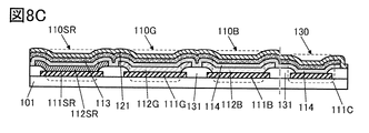
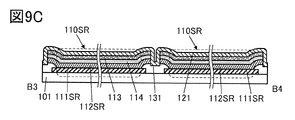
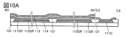
- 10A to 10E are diagrams illustrating an example of a method for manufacturing a display device.
- 11A to 11C are diagrams showing configuration examples of display devices.
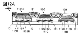
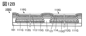
- 12A to 12C are diagrams illustrating configuration examples of display devices.
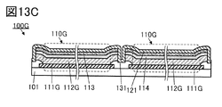
- 13A to 13C are diagrams showing configuration examples of display devices.
- 14A to 14C are top views showing examples of pixels.
- 15A to 15C are cross-sectional views showing examples of display devices.
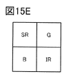
- 15D to 15F are top views showing examples of pixels.
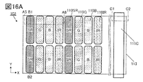
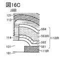
- 16A to 16C are diagrams illustrating configuration examples of display devices.
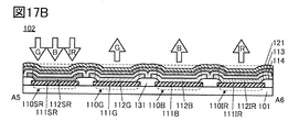
- 17A and 17B are diagrams illustrating configuration examples of a display device.
- 19A to 19D are cross-sectional views showing examples of display devices.
- 20A to 20C are diagrams showing configuration examples of display devices.
- 21A to 21D are diagrams showing configuration examples of display devices.
- FIG. 22 is a perspective view showing an example of a display device.
- 23A and 23B are cross-sectional views showing an example of a display device.
- FIG. 24A is a cross-sectional view showing an example of a display device;
- FIG. 24B is a cross-sectional view showing an example of a transistor;
- 25A and 25B are perspective views showing an example of a display module.
- FIG. 26 is a cross-sectional view showing an example of a display device.
- FIG. 27 is a cross-sectional view showing an example of a display device.
- FIG. 28 is a cross-sectional view showing an example of a display device.
- FIG. 29 is a circuit diagram showing an example of a pixel circuit.
- 30A and 30B are diagrams showing an example of a method of driving a display device.
- 31A to 31D are timing charts showing an example of a method for driving a display device.
- 32A and 32B are timing charts showing an example of the driving method of the display device.
- FIG. 33 is a circuit diagram showing an example of a pixel circuit.
- 34A to 34C are diagrams illustrating examples of functions of electronic devices.
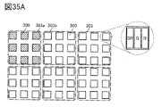
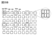
- 35A and 35B are diagrams showing an example of a method of driving a display device.
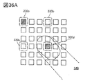
- 36A and 36B are diagrams showing an example of a method of driving a display device.
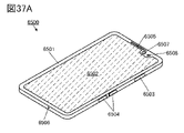
- 37A and 37B are diagrams illustrating examples of electronic devices.
- 38A to 38D are diagrams showing examples of electronic devices.
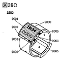
- 39A to 39F are diagrams showing examples of electronic devices.
- film and “layer” can be interchanged depending on the case or situation.
- conductive layer can be changed to the term “conductive film.”
- insulating film can be changed to the term “insulating layer”.
- a display device of one embodiment of the present invention includes a plurality of pixels in a display portion, and the pixels are arranged in a matrix. Each pixel has a light emitting device and a light receiving and emitting device.
- the display portion of the display device of this embodiment has one or both of an imaging function and a sensing function in addition to the function of displaying an image.
- a light-emitting device has a pair of electrodes and an EL layer therebetween.
- the light emitting device is preferably an organic EL device (organic electroluminescence device).
- Two or more light emitting devices that emit different colors have EL layers each containing a different material.
- a full-color display device can be realized by having three types of light-emitting devices that respectively emit red (R), green (G), and blue (B) light.
- an organic EL device that is a light-emitting device and an organic photodiode that is a light-receiving device can be formed on the same substrate. Therefore, an organic photodiode can be incorporated in a display device using an organic EL device.
- the aperture ratio of the pixel may decrease.
- each sub-pixel that emits light of any color is provided with a light emitting/receiving device instead of a light emitting device.
- a light emitting/receiving device has both a function of emitting light (light emitting function) and a function of receiving light (light receiving function). For example, if a pixel has three sub-pixels, a red sub-pixel, a green sub-pixel, and a blue sub-pixel, at least one sub-pixel has a light emitting/receiving device and the other sub-pixels have a light emitting device. Configuration.
- the pixel By having the light receiving/emitting device serve as both a light emitting device and a light receiving device, the pixel can be provided with a light receiving function without increasing the number of sub-pixels included in the pixel. As a result, one or both of an imaging function and a sensing function can be added to the display portion of the display device while maintaining the aperture ratio of the pixel (the aperture ratio of each sub-pixel) and the definition of the display device. .
- a light receiving and emitting device can be produced by combining an organic EL device that is a light emitting device and an organic photodiode that is a light receiving device.
- a light emitting/receiving device can be produced by adding an active layer of an organic photodiode to the laminated structure of the organic EL device.
- a light emitting/receiving device has a pair of electrodes and a light emitting/receiving layer therebetween.
- the light emitting/receiving layer can have a structure including a layer forming the EL layer and an active layer.
- an increase in the number of film forming steps can be suppressed by collectively forming layers that can have a common configuration with the organic EL device.
- one of the pair of electrodes can be a layer common to the light receiving and emitting device and the light emitting device.
- at least one of the hole injection layer, the hole transport layer, the electron transport layer, and the electron injection layer is preferably a layer common to the light receiving and emitting device and the light emitting device.
- the light emitting/receiving device and the light emitting device may have the same configuration except for the presence or absence of the active layer of the light emitting/receiving device. In other words, a light emitting/receiving device can be produced by simply adding an active layer to a light emitting device.
- a display device having a light-receiving and emitting device can be manufactured using an existing display device manufacturing apparatus and manufacturing method.
- a shadow mask such as a metal mask (MM) or a fine metal mask (FMM) is used. Formation by a vapor deposition method is known. However, in this method, island-like formations occur due to various influences such as shadow mask accuracy, positional deviation between the shadow mask and the substrate, shadow mask deflection, and broadening of the contour of the deposited film due to vapor scattering and the like. Since the shape and position of the organic film deviate from the design, it is difficult to achieve high definition and high aperture ratio. Therefore, measures have been taken to artificially increase the definition (also called pixel density) by applying a special pixel arrangement method such as a pentile arrangement.
- a special pixel arrangement method such as a pentile arrangement.
- shadow masks such as metal masks (MM) and fine metal masks (FMM) are sometimes referred to as metal masks (MM).
- a device manufactured using a metal mask (MM) may be referred to as a device with a metal mask (MM) structure.
- a device manufactured without using a metal mask is sometimes called a device with a metal maskless (MML) structure.
- the light-emitting device and the light-emitting device of each color are used to form different light-emitting layers or to paint different light-emitting layers.
- the structure is sometimes called an SBS (Side By Side) structure.
- a light-emitting device capable of emitting white light is sometimes referred to as a white light-emitting device.
- a white light-emitting device can be combined with a colored layer (for example, a color filter) to realize a full-color display device.
- the EL layer and the light receiving/emitting layer are processed into fine patterns without using a metal mask.
- a metal mask As a result, it is possible to realize a display device having a high definition and a large aperture ratio, which has been difficult to achieve in the past.
- the EL layer and the light receiving/emitting layer can be formed separately, a display device with extremely vivid, high contrast, and high display quality can be realized.
- the distance between EL layers of different colors In a formation method using a metal mask, it is difficult to set the distance between EL layers of different colors to less than 10 ⁇ m, for example.
- the layer spacing can be as narrow as 3 ⁇ m or less, 2 ⁇ m or less, or even 1 ⁇ m or less.
- the gap can be narrowed to 500 nm or less, 200 nm or less, 100 nm or less, or even 50 nm or less.
- the distance between the EL layer and the light emitting/receiving layer can also be narrowed to 8 ⁇ m or less, 5 ⁇ m or less, or 3 ⁇ m or less.
- the area of non-light-emitting regions that may exist between two light-emitting devices and between a light-receiving and light-emitting device and a light-emitting device can be significantly reduced, and the aperture ratio can be brought close to 100%.
- the aperture ratio can be 50% or more, 60% or more, 70% or more, 80% or more, or even 90% or more, and less than 100%.
- the patterns of the EL layer and the light emitting/receiving layer can also be made extremely small compared to the case of using a metal mask.
- the thickness varies between the center and the edge of the pattern. area becomes smaller.
- the pattern is formed by processing a film formed to have a uniform thickness, the thickness can be made uniform within the pattern, and even if the pattern is fine, almost the entire area of the pattern can emit light. It can be used as a region. Therefore, according to the above manufacturing method, both high definition and high aperture ratio can be achieved.
- a display device in which fine light receiving and emitting devices and light emitting devices are integrated can be realized. Since there is no need to increase the definition, a so-called stripe arrangement in which R, G, and B are arranged in one direction, and a resolution of 500 ppi or more, 1000 ppi or more, or 2000 ppi or more, further 3000 ppi or more, further 5000 ppi or more. A high-definition display can be realized.
- the layers included in the light receiving and emitting device may have different functions depending on whether the light receiving or emitting device functions as a light receiving device or as a light emitting device. Components are referred to herein based on their function when the light receiving and emitting device functions as a light emitting device.
- the hole injection layer functions as a hole injection layer when the light emitting/receiving device functions as a light emitting device, and functions as a hole transport layer when the light emitting/receiving device functions as a light receiving device.
- the electron injection layer functions as an electron injection layer when the light emitting/receiving device functions as a light emitting device, and functions as an electron transport layer when the light emitting/receiving device functions as a light receiving device.
- the display device of the present embodiment has a light emitting/receiving device and a light emitting device in the display section. Specifically, light receiving and emitting devices and light emitting devices are arranged in a matrix in the display section. Therefore, the display unit has one or both of an imaging function and a sensing function in addition to the function of displaying an image.
- the display unit can be used for one or more of an image sensor or a touch sensor. That is, by detecting light with the display portion, an image can be captured, or proximity or contact of an object (a finger, a pen, or the like) can be detected. Furthermore, the display device of this embodiment mode can use a light-emitting device as a light source of a sensor. Therefore, it is not necessary to provide a light receiving portion and a light source separately from the display device, and the number of parts of the electronic device can be reduced.
- the light-receiving and emitting device when an object reflects light emitted from a light-emitting device included in the display portion, the light-receiving and emitting device can detect the reflected light. detection is possible.
- the display device of this embodiment has a function of displaying an image using a light emitting device and a light emitting/receiving device.
- the light-emitting device and the light-receiving and emitting device function as display devices (also referred to as display elements).
- the light-emitting device is preferably an EL device such as OLED (Organic Light Emitting Diode) or QLED (Quantum-dot Light Emitting Diode).
- EL devices include substances that emit fluorescence (fluorescent materials), substances that emit phosphorescence (phosphorescent materials), inorganic compounds (quantum dot materials, etc.), and substances that exhibit heat-activated delayed fluorescence (heat-activated delayed fluorescence ( Thermally Activated Delayed Fluorescence (TADF) material) and the like.
- LEDs such as micro LED (Light Emitting Diode), can also be used as a light emitting device.
- the light-emitting substance included in the light-receiving and emitting device can also be the above-described substances.
- the display device of this embodiment has a function of detecting light using a light emitting/receiving device.
- the display device of this embodiment can capture an image using the light emitting/receiving device.
- the display device of this embodiment can be used as a scanner.
- an image sensor can be used to acquire data such as fingerprints or palm prints.
- a biometric sensor can be built in the display device of this embodiment mode.
- an image sensor it is possible to acquire data such as the user's facial expression, eye movements, or changes in pupil diameter.
- data such as the user's facial expression, eye movements, or changes in pupil diameter.
- analyzing the data it is possible to obtain information about the user's mind and body.
- By changing the output content of one or both of the display and audio based on the information for example, in a device for VR (Virtual Reality), a device for AR (Augmented Reality), or a device for MR (Mixed Reality), It is possible to ensure that the user can use the equipment safely.
- VR Virtual Reality
- AR Augmented Reality
- MR Mated Reality
- the display device of the present embodiment can detect proximity or contact of an object using the light emitting/receiving device.
- the light emitting/receiving device functions as a photoelectric conversion device that detects light incident on the light emitting/receiving device and generates electric charge.
- the amount of charge generated is determined based on the amount of incident light.
- a light emitting/receiving device can be produced by adding an active layer to the structure of the light emitting device described above.
- the light receiving and emitting device can use, for example, the active layer of a pn-type or pin-type photodiode.
- Organic photodiodes can be easily made thinner, lighter, and larger, and have a high degree of freedom in shape and design, so that they can be applied to various display devices.
- FIGS. 1A to 1D are cross-sectional views of a display device of one embodiment of the present invention.
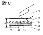
- a display device 50A shown in FIG. 1A has a layer 53 having a light receiving/emitting device and a layer 57 having a light emitting device between a substrate 51 and a substrate 59 .
- a display device 50B shown in FIG. 1B has, between a substrate 51 and a substrate 59, a layer 53 having a light emitting/receiving device, a layer 57 having a light emitting device, and a layer 55 having a transistor.
- layer 53 with light receiving and emitting devices and layer 57 with light emitting devices can be provided over layer 55 with transistors.
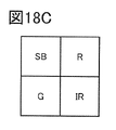
- green (G) light and blue (B) light are emitted from the layer 57 having the light emitting device, and red (R) light is emitted from the layer 53 having the light receiving and emitting device.
- It is a configuration that is 1A and 1B show green (G) light and blue (B) light emitted from layer 57, red (R) light emitted from layer 53, and light incident on layer 53, respectively. It is schematically indicated by an arrow. Note that in the display device of one embodiment of the present invention, the color of light emitted from the layer 53 including light emitting/receiving devices is not limited to red.
- the light emitting/receiving device included in layer 53 can detect light incident from the outside of display device 50A or display device 50B. For example, when the light emitting/receiving device emits red (R) light, the light emitting/receiving device can detect one or both of green (G) light and blue (B) light. .
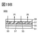
- the wavelength region of blue (B) is 400 nm or more and less than 490 nm, and blue (B) light has at least one emission spectrum peak in this wavelength region.
- the wavelength region of green (G) is 490 nm or more and less than 580 nm, and green (G) light has at least one emission spectrum peak in this wavelength region.
- the wavelength region of red (R) is 580 nm or more and less than 700 nm, and red (R) light has at least one emission spectrum peak in this wavelength region.
- the wavelength region of visible light is from 400 nm to less than 700 nm, and visible light has at least one emission spectrum peak in this wavelength region.
- the infrared (IR) wavelength range is from 700 nm to less than 900 nm, and the infrared (IR) light has at least one emission spectrum peak in this wavelength range.
- the light receiving and emitting device preferably has sensitivity in the wavelength region to be detected. For example, if the light receiving and emitting device has sensitivity in the blue (B) wavelength region, the light receiving and emitting device can detect blue (B) light.
- a display device of one embodiment of the present invention includes a plurality of pixels arranged in a matrix.
- One pixel has one or more sub-pixels.
- One sub-pixel has one light receiving/emitting device or one light emitting device.
- a pixel has three sub-pixels (three colors of R, G, and B, or three colors of yellow (Y), cyan (C), and magenta (M)), or sub-pixels (4 colors of R, G, B, and white (W), or 4 colors of R, G, B, Y, etc.) can be applied.
- At least one color subpixel has a light receiving and emitting device.
- the light emitting/receiving device may be provided in all the pixels or may be provided in some of the pixels.
- one pixel may have a plurality of light receiving and emitting devices.
- the layer 55 having transistors has, for example, a transistor electrically connected to a light emitting/receiving device and a transistor electrically connected to a light emitting device.
- the layer 55 having transistors may further have wirings, electrodes, terminals, capacitors, resistors, and the like.
- a display device of one embodiment of the present invention may have a function of detecting an object such as a finger in contact with the display device. Alternatively, it may have a function of detecting an object that is close to (not in contact with) the display device.
- FIG. 1C shows how the finger 52 is in contact with the display device 50B.
- FIG. 1D shows a finger 52 in close proximity to the display device 50B.
- light emitted by light emitting devices on layer 57 is reflected by finger 52 in contact with or in close proximity to display 50B, and the reflected light is detected by light receiving and emitting devices on layer 53. . This makes it possible to detect that the finger 52 is in contact with or close to the display device 50B.
- the display device 50A and the display device 50B can also function as a touch panel or a pen tablet using light emitting/receiving devices.
- a light emitting/receiving device By using a light emitting/receiving device, it is possible to detect the position of an object with high insulation, unlike the case where a capacitive touch sensor or an electromagnetic induction type touch sensor is used.
- stylus, etc. and various writing utensils (for example, writing brushes, glass pens, quill pens, etc.) can also be used.
- FIGS. 1E to 1H Examples of pixels are shown in FIGS. 1E to 1H.
- the pixels shown in FIG. 1E employ so-called stripe array sub-pixels in which light-emitting devices or light-receiving and light-receiving devices that emit light of the same color are arranged in one direction.
- the pixel has a sub-pixel (SR) that emits red light and has a light-receiving function, a sub-pixel (G) that emits green light, and a sub-pixel (B) that emits blue light.
- SR sub-pixel
- G that emits green light
- B sub-pixel
- the pixel A display device having a light-receiving function can be manufactured.
- the light emitted from the light source is less visible to the user. Since blue light has lower visibility than green light, it is preferable to use a light-emitting device that emits blue light as a light source. Therefore, the light receiving and emitting device preferably has a function of receiving blue light.
- the pixels shown in FIG. 1F are applied with sub-pixels arranged in a matrix.
- a sub-pixel (SR) that emits red light and has a light receiving function
- a sub-pixel (G) that emits green light
- a sub-pixel (G) that emits blue light
- a sub-pixel (W) for emitting white light.
- the light-emitting device used for the red (R) sub-pixel may be replaced with the light-receiving and emitting device. By replacing with , a display device having a light-receiving function in a pixel can be manufactured.
- the pixels shown in FIG. 1G are sub-pixels (SR) that emit red light and have a light-receiving function, sub-pixels (G) that emit green light, and sub-pixels (B) that emit blue light. ).
- the sub-pixels (SR) are arranged in different columns from the sub-pixels (G) and the sub-pixels (B).
- the sub-pixels (G) and sub-pixels (B) are alternately arranged in the same column, one being provided in odd rows and the other being provided in even rows. Note that the color of sub-pixels arranged in a column different from sub-pixels of other colors is not limited to red (R), and may be green (G) or blue (B).
- FIG. 1H shows two pixels, one pixel being composed of three sub-pixels surrounded by dotted lines.
- the pixel shown in FIG. 1H includes a sub-pixel (SR) that emits red light and has a light receiving function, a sub-pixel (G) that emits green light, and a sub-pixel (B) that emits blue light. ).
- SR sub-pixel
- G sub-pixel
- B sub-pixel
- the sub-pixel (G) is arranged in the same row as the sub-pixel (SR), and the sub-pixel (B) is arranged in the same column as the sub-pixel (G).
- sub-pixels (SR), sub-pixels (G), and sub-pixels (B) are repeatedly arranged in both odd-numbered rows and even-numbered rows.
- Sub-pixels of different colors are arranged in rows and even-numbered rows.
- the arrangement of sub-pixels is not limited to the order shown in FIGS. 1E to 1H.
- the positions of the sub-pixel (B) and the sub-pixel (G) may be reversed.
- FIGS. 1E to 1H show examples in which subpixels of each color have the same area, one embodiment of the present invention is not limited to this.
- the area of the sub-pixel may differ depending on the color.
- FIGS. 1E to 1H show the structures in which the subpixels having a light-receiving function emit red (R) light
- R red
- a pixel may have a sub-pixel (B) that emits green light and has a light-receiving function, a sub-pixel that emits red light, and a sub-pixel (B) that emits blue light.
- the display device of this embodiment does not need to change the pixel arrangement in order to incorporate the light receiving function into the pixels, and can have one or both of the imaging function and the sensing function in the display portion without reducing the aperture ratio and definition. can be added.
- FIG. 2A A schematic top view of a display device 100 of one embodiment of the present invention is shown in FIG. 2A.
- the display device 100 includes a plurality of light emitting/receiving devices 110SR that emit red light and have a light receiving function, a plurality of light emitting devices 110G that emit green light, and a plurality of light emitting devices 110B that emit blue light.
- the light receiving and light emitting regions of each light emitting/receiving device are denoted by SR, and the light emitting regions of each light emitting device are denoted by G and B. ing.
- the light receiving/emitting device 110SR, the light emitting device 110G, and the light emitting device 110B are arranged in a matrix.
- FIG. 2A shows an example of a display device having the stripe arrangement shown in FIG. 1E. Note that the arrangement of the light emitting devices is not limited to this, and a delta arrangement or a zigzag arrangement may be applied. Alternatively, a pentile array can be used.
- the light receiving/emitting device 110SR, the light emitting device 110G, and the light emitting device 110B are arranged in the X direction.
- light emitting devices of the same color are arranged in the Y direction that intersects with the X direction.
- FIG. 2B is a schematic cross-sectional view corresponding to the dashed-dotted line A1-A2 in FIG. 2A
- FIG. 2C is a schematic cross-sectional view corresponding to the dashed-dotted line B1-B2.
- FIG. 2B shows cross sections of the light emitting/receiving device 110SR, the light emitting device 110G, and the light emitting device 110B.
- the light emitting/receiving device 110 SR has a pixel electrode 111 SR, a light emitting/receiving layer 112 SR, a layer 114 and a common electrode 113 .
- the light emitting device 110G has a pixel electrode 111G, an EL layer 112G, a layer 114 and a common electrode 113.
- FIG. Light-emitting device 110B has pixel electrode 111B, EL layer 112B, layer 114, and common electrode 113.
- the layer 114 and the common electrode 113 are commonly provided for the light emitting/receiving device 110SR, the light emitting device 110G, and the light emitting device 110B.
- Layer 114 may also be referred to as a common layer.
- the light emitting/receiving layer 112SR of the light emitting/receiving device 110SR has a light-emitting organic compound having an emission spectrum peak at least in the red wavelength region.
- the EL layer 112G included in the light-emitting device 110G includes a light-emitting organic compound having an emission spectrum peak at least in the green wavelength region.
- the EL layer 112B included in the light-emitting device 110B includes a light-emitting organic compound having an emission spectrum peak at least in the blue wavelength region.
- the light emitting/receiving layer 112SR, the EL layer 112G, and the EL layer 112B each include a layer containing a light-emitting organic compound (light-emitting layer), an electron injection layer, an electron transport layer, a hole injection layer, and a hole transport layer.
- a light-emitting organic compound light-emitting layer
- layer 114 comprises one or more of an electron injection layer, an electron transport layer, a hole injection layer, and a hole transport layer.
- a pixel electrode 111SR, a pixel electrode 111G, and a pixel electrode 111B are provided for each light emitting device.
- the common electrode 113 and the layer 114 are provided as a continuous layer common to each light emitting device.
- a conductive film having a property of transmitting visible light is used for one of the pixel electrodes and the common electrode 113, and a conductive film having a reflective property is used for the other.
- An insulating layer 131 is provided to cover end portions of the pixel electrode 111SR, the pixel electrode 111G, and the pixel electrode 111B.
- the ends of the insulating layer 131 are preferably tapered.
- a tapered shape refers to a shape in which at least a part of the side surface of the structure is inclined with respect to the substrate surface.
- the insulating layer 131 may be omitted if unnecessary.
- the light emitting/receiving layer 112SR, the EL layer 112G, and the EL layer 112B each have a region in contact with the top surface of the pixel electrode and a region in contact with the surface of the insulating layer 131 . Further, end portions of the light receiving and emitting layer 112 SR, the EL layer 112 G, and the EL layer 112 B are located on the insulating layer 131 .
- a gap is provided between the two EL layers between the light emitting devices of different colors.
- the light receiving and emitting layer 112SR, the EL layer 112G, and the EL layer 112G are preferably provided so as not to be in contact with each other. This can suitably prevent current from flowing through two adjacent EL layers and causing unintended light emission. Therefore, the contrast can be increased, and a display device with high display quality can be realized.
- the light emitting/receiving layers 112SR are formed in strips so that the light emitting/receiving layers 112SR are continuous in the Y direction.
- the light emitting/receiving layers 112SR and the like are formed in strips so that the light emitting/receiving layers 112SR are continuous in the Y direction.
- FIG. 2C shows the cross section of the light emitting/receiving device 110SR as an example, but the light emitting device 110G and the light emitting device 110B can also have the same shape.
- a protective layer 121 is provided on the common electrode 113 to cover the light emitting/receiving device 110SR, the light emitting device 110G, and the light emitting device 110B.
- the protective layer 121 has a function of preventing impurities such as water from diffusing into each light-emitting device from above.
- the protective layer 121 can have, for example, a single layer structure or a laminated structure including at least an inorganic insulating film.
- inorganic insulating films include oxide films and nitride films such as silicon oxide films, silicon oxynitride films, silicon nitride oxide films, silicon nitride films, aluminum oxide films, aluminum oxynitride films, and hafnium oxide films.
- a semiconductor material such as indium gallium oxide or indium gallium zinc oxide may be used for the protective layer 121 .
- a laminated film of an inorganic insulating film and an organic insulating film can also be used as the protective layer 121 .
- a structure in which an organic insulating film is sandwiched between a pair of inorganic insulating films is preferable.
- the organic insulating film functions as a planarizing film.
- the upper surface of the organic insulating film can be flattened, so that the coverage of the inorganic insulating film thereon can be improved, and the barrier property can be enhanced.
- the upper surface of the protective layer 121 is flat, when a structure (for example, a color filter, an electrode of a touch sensor, or a lens array) is provided above the protective layer 121, an uneven shape due to the structure below may be formed. This is preferable because it can reduce the impact.
- a structure for example, a color filter, an electrode of a touch sensor, or a lens array
- connection electrode 111C electrically connected to the common electrode 113.
- the connection electrode 111C is given a potential (for example, an anode potential or a cathode potential) to be supplied to the common electrode 113 .
- the connection electrodes 111C are provided outside the display area where the light emitting/receiving devices 110SR and the like are arranged. Note that FIG. 2A shows the common electrode 113 with a dashed line.
- connection electrodes 111C can be provided along the periphery of the display area. For example, it may be provided along one side of the periphery of the display area, or may be provided over two or more sides of the periphery of the display area. That is, when the top surface shape of the display area is rectangular, the top surface shape of the connection electrode 111C can be strip-shaped, L-shaped, U-shaped with corners (square bracket-shaped), square, or the like. . Moreover, the top surface shape of the display area is not limited to a rectangle, and may be polygonal or curved. In that case, the top surface shape of the connection electrode 111C may be a shape along a part of the periphery of the display area.
- FIG. 2D is a schematic cross-sectional view corresponding to the dashed-dotted line C1-C2 in FIG. 2A.
- FIG. 2D shows a connection portion 130 where the connection electrode 111C and the common electrode 113 are electrically connected.
- the common electrode 113 is provided on the connection electrode 111 ⁇ /b>C so as to be in contact therewith, and the protective layer 121 is provided to cover the common electrode 113 .
- An insulating layer 131 is provided to cover the end of the connection electrode 111C.
- a display device of one embodiment of the present invention is a top-emission type in which light is emitted in a direction opposite to the substrate over which the light receiving and emitting device and the light emitting device are formed, and light is emitted toward the substrate over which the light receiving and emitting device and the light emitting device are formed.
- Either a bottom emission type that emits light or a dual emission type that emits light from both sides may be used.
- a top-emission display device will be taken as an example. Also, in both the light receiving and emitting device and the light emitting device, the pixel electrode 111 functions as an anode and the common electrode 113 functions as a cathode.
- the light emitting device 110 may be referred to when describing items common to the light emitting device 110G and the light emitting device 110B.
- the pixel electrode 111 may be referred to when describing items common to the pixel electrode 111SR, the pixel electrode 111G, and the pixel electrode 111B.
- FIG. 3A An enlarged view of the region 10SR indicated by a dashed line in FIG. 2B is shown in FIG. 3A, an enlarged view of the region 10G is shown in FIG. 3B, and an enlarged view of the region 10B is shown in FIG. 3C.
- the light emitting/receiving device 110SR has a pixel electrode 111SR, a light emitting/receiving layer 112SR, a layer 114, and a common electrode 113 stacked in this order.
- the light emitting/receiving layer 112SR has at least an active layer 573 and a light emitting layer 583R.
- the light emitting layer 583R has a light emitting material that emits red light.
- the active layer 573 and the light emitting layer 583R may be in contact with each other.
- the light emitting/receiving layer 112SR has a hole injection layer 581, a hole transport layer 582, an active layer 573, a light emitting layer 583R, and an electron transport layer 584 laminated in this order.
- Layer 114 can use an electron injection layer. Note that the layer 114 may have a stacked structure of an electron-transporting layer and an electron-injecting layer on the electron-transporting layer. Note that the light emitting/receiving layer 112SR may not include at least one of the hole injection layer 581, the hole transport layer 582, and the electron transport layer 584. In addition, the light emitting/receiving layer 112SR may have other layers such as a hole blocking layer and an electron blocking layer.
- the active layer 573 contains a semiconductor.
- the semiconductor include inorganic semiconductors such as silicon and organic semiconductors including organic compounds.
- An organic semiconductor can be preferably used as the semiconductor included in the active layer 573 .
- the active layer 573 has an n-type semiconductor material and a p-type semiconductor material.
- the active layer 573 can have a structure (bulk heterojunction structure) having a mixed layer of an n-type semiconductor material and a p-type semiconductor material.
- the active layer 573 can be formed by co-depositing an n-type semiconductor material and a p-type semiconductor material.
- the active layer 573 may have a laminated structure (bilayer structure) of a layer containing an n-type semiconductor material and a layer containing a p-type semiconductor material.
- a structure other than the bulk heterojunction structure and the bilayer structure may be applied to the active layer 573 .
- the layers constituting the light emitting/receiving layer 112SR have their end portions aligned or substantially aligned with each other.
- the top surface shapes of the layers forming the light emitting/receiving layer 112SR match or substantially match each other.
- the positions of the ends of the hole injection layer 581, the hole transport layer 582, the active layer 573, the light emitting layer 583R, and the electron transport layer 584 match or substantially match each other.
- the top surface shapes of the hole injection layer 581, the hole transport layer 582, the active layer 573, the light emitting layer 583R, and the electron transport layer 584 match or substantially match each other.
- the upper surface shapes match or roughly match means that at least part of the contours overlaps between the laminated layers.
- the upper layer and the lower layer may be processed with the same mask pattern or partially with the same mask pattern. Strictly speaking, however, the outlines do not overlap, and the upper layer may be located inside the lower layer, or the upper layer may be located outside the lower layer.
- the light-emitting device 110G has a pixel electrode 111G, an EL layer 112G, a layer 114, and a common electrode 113 stacked in this order.
- the EL layer 112G has at least a light emitting layer 583G.
- the light-emitting layer 583G has a light-emitting material that emits green light.
- FIG. 3B shows an example in which the EL layer 112G has a hole-injection layer 581, a hole-transport layer 582, a light-emitting layer 583G, and an electron-transport layer 584 stacked in this order.
- the layers constituting the EL layer 112G have their end portions aligned or substantially aligned with each other.
- the layers forming the EL layer 112G match or substantially match each other in top surface shape.
- the positions of the ends of the hole injection layer 581, the hole transport layer 582, the light emitting layer 583G, and the electron transport layer 584 match or substantially match each other.
- the top surface shapes of the hole-injection layer 581, the hole-transport layer 582, the light-emitting layer 583G, and the electron-transport layer 584 match or substantially match each other.
- the light-emitting device 110B has a pixel electrode 111B, an EL layer 112B, a layer 114, and a common electrode 113 stacked in this order.
- the EL layer 112B has at least a light emitting layer 583B.
- the light-emitting layer 583B has a light-emitting substance that emits blue light.
- FIG. 3C shows an example in which the EL layer 112B has a hole-injection layer 581, a hole-transport layer 582, a light-emitting layer 583G, and an electron-transport layer 584 stacked in this order.
- the layers constituting the EL layer 112B have ends that are aligned or substantially aligned with each other.
- the layers forming the EL layer 112B have the same or approximately the same top surface shape.
- the positions of the ends of the hole injection layer 581, the hole transport layer 582, the light emitting layer 583B, and the electron transport layer 584 match or substantially match each other.
- the top surface shapes of the hole-injection layer 581, the hole-transport layer 582, the light-emitting layer 583B, and the electron-transport layer 584 match or substantially match each other.
- the active layer 573 contains an organic compound different from any of the organic compound contained in the light-emitting layer 583R, the organic compound contained in the light-emitting layer 583G, and the organic compound contained in the light-emitting layer 583B.
- the light-emitting layer 583R contains an organic compound different from any of the organic compound contained in the active layer 573, the organic compound contained in the light-emitting layer 583G, and the organic compound contained in the light-emitting layer 583B.
- the light-emitting layer 583G contains an organic compound different from any of the organic compound contained in the active layer 573, the organic compound contained in the light-emitting layer 583R, and the organic compound contained in the light-emitting layer 583B.
- the light-emitting layer 583B contains an organic compound different from any of the organic compound contained in the active layer 573, the organic compound contained in the light-emitting layer 583R, and the organic compound contained in the light-emitting layer 583G.
- the wavelength range of light emitted by the light emitting layer 583R, the wavelength range of light emitted by the light emitting layer 583G, and the wavelength range of light emitted by the light emitting layer 583B are different from each other.
- the organic compound included in the active layer 573 has sensitivity to one or a plurality of wavelength regions of light emitted from the light-emitting layer 583G and light emitted from the light-emitting layer 583B.
- the hole-injection layer 581 is an electron-injection layer
- the hole-transport layer 582 is an electron-injection layer.
- the transport layer, electron transport layer 584 may be replaced by a hole transport layer
- layer 114 may be replaced by a hole injection layer.
- layer 114 may be replaced with a hole transport layer. Note that a structure without the layer 114 may be employed.
- Light-emitting devices can be broadly classified into single structures and tandem structures.
- a single structure device has one light emitting unit between a pair of electrodes.
- a light-emitting unit has at least one or more light-emitting layers.
- the light emitting unit may further have one or more functional layers such as a hole injection layer, a hole transport layer, an electron transport layer and an electron injection layer.
- the light-emitting layers should be selected such that the light emitted from each of the two light-emitting layers has a complementary color relationship.
- the luminescent color of the first luminescent layer and the luminescent color of the second luminescent layer have a complementary color relationship, it is possible to obtain a configuration in which the entire light emitting device emits white light. Further, in the case of a light-emitting device having three or more light-emitting layers, it is possible to adopt a structure that emits white light by mixing the light-emitting colors of the respective light-emitting layers.
- a tandem structure device preferably has two or more light-emitting units between a pair of electrodes, and each light-emitting unit preferably includes one or more light-emitting layers.
- each light-emitting unit preferably includes one or more light-emitting layers.
- the light from the light emitting layers of a plurality of light emitting units may be combined to obtain white light emission.
- the structure for obtaining white light emission is the same as the structure of the single structure.
- an intermediate layer such as a charge generation layer is provided between a plurality of light emitting units.
- the light emitting device having the SBS structure can consume less power than the white light emitting device. can. If it is desired to keep power consumption low, it is preferable to use a light-emitting device with an SBS structure.
- the white light emitting device is preferable because the manufacturing process is simpler than that of the SBS structure light emitting device, so that the manufacturing cost can be lowered or the manufacturing yield can be increased.
- FIG. 3B and the like show an example in which the light-emitting device has a single structure, one embodiment of the present invention is not limited to this.
- a tandem structure may be applied to the light emitting device.
- the light emitting/receiving device 110SR, the light emitting device 110G, and the light emitting device 110B are electroluminescence devices that emit light toward the common electrode 113 by applying a voltage between the pixel electrode 111 and the common electrode 113, respectively.
- the light emitting/receiving device 110SR also functions as a photoelectric conversion element (also referred to as a photoelectric conversion device) that detects light incident on the light emitting/receiving device 110SR and generates charges.
- the light emitting/receiving device 110SR can extract electric charges generated by light incident on the active layer 573 as current. At this time, a voltage may be applied between the pixel electrode 111 and the common electrode 113 . The amount of charge is determined based on the amount of light incident on the light emitting/receiving device 110SR.
- the light emitting/receiving device 110SR has a function of detecting one or more of visible light and infrared light.
- an organic compound is used for the active layer 573 of the light emitting/receiving device 110SR.
- the light emitting/receiving device 110SR can share layers other than the active layer 573 and the light emitting layer 583R with the light emitting device 110G and the light emitting device 110B. Therefore, the light emitting/receiving device 110SR can be formed in parallel with the formation of the light emitting device simply by adding the step of forming the active layer 573 to the manufacturing process of the light emitting device. Also, the light emitting device and the light receiving and emitting device 110SR can be formed on the same substrate. Therefore, the light emitting/receiving device 110SR can be incorporated in the display device without significantly increasing the number of manufacturing steps.
- the active layer 573 and the light emitting layer 583R of the light emitting and receiving device 110SR, the light emitting layer 583G of the light emitting device 110G, and the light emitting layer 583B of the light emitting device 110B are separately manufactured, except that the light emitting and receiving device 110SR and the light emitting device is a common configuration.
- the configurations of the light emitting/receiving device 110SR and the light emitting device are not limited to this.
- the light emitting/receiving device 110SR and the light emitting device may have layers other than the active layer 573 and the light emitting layer 583 that are made separately from each other.
- the light emitting/receiving device 110SR and the light emitting device preferably have at least one layer (common layer) used in common. Accordingly, the light emitting/receiving device 110SR can be incorporated in the display device without significantly increasing the number of manufacturing steps.
- the light emitting/receiving device 110SR By sharing part of the configuration of the light emitting/receiving device 110SR and the light emitting device, it is possible to reduce the margin for misalignment compared to the case where all the configurations of the light emitting/receiving device, 110SR, and light emitting device are made separately. Thereby, the aperture ratio of the pixel can be increased, and the light extraction efficiency of the display device can be increased. This can extend the life of the light emitting/receiving device 110SR and the light emitting device. In addition, a high-luminance display device can be realized. Moreover, a high-definition display device can be realized.
- a conductive film that transmits visible light is used for the electrodes on the light extraction side and the light incidence side.
- a conductive film that reflects visible light is preferably used for the electrode on the side from which light is not extracted and from which light is not incident.
- a micro optical resonator (microcavity) structure is preferably applied to the light emitting device included in the display device of this embodiment. Therefore, one of the pair of electrodes of the light-emitting device preferably has an electrode (semi-transmissive/semi-reflective electrode) that is transparent and reflective to visible light, and the other is an electrode that is reflective to visible light ( reflective electrode). Since the light-emitting device has a microcavity structure, the light emitted from the light-emitting layer can be resonated between the two electrodes, and the light emitted from the light-emitting device can be enhanced.
- a microcavity structure may be applied to the light receiving and emitting device.
- the semi-transmissive/semi-reflective electrode can be configured to include, for example, a reflective conductive material and a translucent conductive material.
- the light transmittance of the transparent electrode is set to 40% or more.
- an electrode having a visible light transmittance of 40% or more is preferably used for a light-emitting device.
- the visible light reflectance of the semi-transmissive/semi-reflective electrode is 10% or more and 95% or less, preferably 30% or more and 80% or less.
- the visible light reflectance of the reflective electrode is 40% or more and 100% or less, preferably 70% or more and 100% or less.
- the resistivity of these electrodes is preferably 1 ⁇ 10 ⁇ 2 ⁇ cm or less.
- the light receiving and emitting device and the light emitting device each have at least a light emitting layer 583 .
- layers other than the light-emitting layer 583 include a substance with a high hole-injection property, a substance with a high hole-transport property, a hole-blocking material, a substance with a high electron-transport property, and a substance with an electron-injection property.
- a layer containing a high-density substance, an electron-blocking material, a bipolar substance (a substance with high electron-transport properties and high hole-transport properties), or the like may be further included.
- the light-emitting device and the light-receiving and emitting device may have one or more layers in common among the hole injection layer, the hole transport layer, the electron transport layer, and the electron injection layer.
- the light-emitting device and the light-receiving and emitting device can each have one or more different layers among the hole injection layer, the hole transport layer, the electron transport layer, and the electron injection layer.
- the hole-injecting layer is a layer that injects holes from the anode into the hole-transporting layer, and contains a material with high hole-injecting properties.
- a composite material containing a hole-transporting material (for example, an aromatic amine compound) and an acceptor material (electron-accepting material) can be used as the highly hole-injecting material.
- a hole-transporting layer is a layer that transports holes injected from the anode to the light-emitting layer by means of a hole-injecting layer.
- the hole-transporting layer is a layer that transports holes generated by incident light in the active layer to the anode.
- a hole-transporting layer is a layer containing a hole-transporting material.
- the hole-transporting material is preferably a substance having a hole mobility of 1 ⁇ 10 ⁇ 6 cm 2 /Vs or more. Note that substances other than these can be used as long as they have a higher hole-transport property than electron-transport property.
- the hole-transporting material is a highly hole-transporting material such as a ⁇ -electron-rich heteroaromatic compound (e.g., carbazole derivative, thiophene derivative, furan derivative, etc.) or aromatic amine (compound having an aromatic amine skeleton). is preferred.
- a ⁇ -electron-rich heteroaromatic compound e.g., carbazole derivative, thiophene derivative, furan derivative, etc.
- aromatic amine compound having an aromatic amine skeleton
- an electron-transporting layer is a layer that transports electrons injected from the cathode to the light-emitting layer by the electron-injecting layer.
- the electron-transporting layer is a layer that transports electrons generated by incident light in the active layer to the cathode.
- the electron-transporting layer is a layer containing an electron-transporting material.
- the electron-transporting material is preferably a substance having an electron mobility of 1 ⁇ 10 ⁇ 6 cm 2 /Vs or more. Note that substances other than these substances can be used as long as they have a higher electron-transport property than hole-transport property.
- Electron-transporting materials include metal complexes having a quinoline skeleton, metal complexes having a benzoquinoline skeleton, metal complexes having an oxazole skeleton, metal complexes having a thiazole skeleton, oxadiazole derivatives, triazole derivatives, imidazole derivatives, and oxazole. derivatives, thiazole derivatives, phenanthroline derivatives, quinoline derivatives with quinoline ligands, benzoquinoline derivatives, quinoxaline derivatives, dibenzoquinoxaline derivatives, pyridine derivatives, bipyridine derivatives, pyrimidine derivatives, and other nitrogen-containing heteroaromatic compounds.
- a material having a high electron-transport property such as a heteroaromatic compound can be used.
- the electron injection layer is a layer that injects electrons from the cathode to the electron transport layer, and is a layer that contains a material with high electron injection properties.
- Alkali metals, alkaline earth metals, or compounds thereof can be used as materials with high electron injection properties.
- a composite material containing an electron-transporting material and a donor material (electron-donating material) can also be used as the material with high electron-injecting properties.
- the light-emitting layer 583 is a layer containing a light-emitting substance.
- Emissive layer 583 can have one or more luminescent materials.
- a light-emitting substance a substance emitting light of blue, purple, blue-violet, green, yellow-green, yellow, orange, red, or the like is used as appropriate.
- a substance that emits infrared light can also be used as the light-emitting substance.
- Examples of light-emitting substances include fluorescent materials, phosphorescent materials, TADF materials, and quantum dot materials.
- fluorescent materials include pyrene derivatives, anthracene derivatives, triphenylene derivatives, fluorene derivatives, carbazole derivatives, dibenzothiophene derivatives, dibenzofuran derivatives, dibenzoquinoxaline derivatives, quinoxaline derivatives, pyridine derivatives, pyrimidine derivatives, phenanthrene derivatives, naphthalene derivatives, and the like. .
- a phosphorescent material for example, a 4H-triazole skeleton, a 1H-triazole skeleton, an imidazole skeleton, a pyrimidine skeleton, a pyrazine skeleton, or an organometallic complex (especially an iridium complex) having a pyridine skeleton, or a phenylpyridine derivative having an electron-withdrawing group is coordinated.
- Organometallic complexes particularly iridium complexes
- platinum complexes, rare earth metal complexes and the like can be mentioned.
- the light-emitting layer 583 may contain one or more organic compounds (host material, assist material, etc.) in addition to the light-emitting substance (guest material).
- One or both of a hole-transporting material and an electron-transporting material can be used as the one or more organic compounds.
- Bipolar materials or TADF materials may also be used as one or more organic compounds.
- the light-emitting layer 583 preferably includes, for example, a phosphorescent material and a combination of a hole-transporting material and an electron-transporting material that easily form an exciplex.
- ExTET Exciplex-Triplet Energy Transfer
- a combination that forms an exciplex that emits light that overlaps with the wavelength of the absorption band on the lowest energy side of the light-emitting substance energy transfer becomes smooth and light emission can be efficiently obtained.
- high efficiency, low-voltage driving, and long life of the light receiving and emitting device and the light emitting element can be realized at the same time.
- the HOMO level (highest occupied orbital level) of the hole-transporting material is equal to or higher than the HOMO level of the electron-transporting material.
- the LUMO level (lowest unoccupied molecular orbital level) of the hole-transporting material is equal to or higher than the LUMO level of the electron-transporting material.
- the LUMO and HOMO levels of a material can be derived from the material's electrochemical properties (reduction and oxidation potentials) measured by cyclic voltammetry (CV) measurements.
- Formation of the exciplex is performed by comparing, for example, the emission spectrum of the hole-transporting material, the emission spectrum of the electron-transporting material, and the emission spectrum of a mixed film in which these materials are mixed, and the emission spectrum of the mixed film is the emission spectrum of each material. It can be confirmed by observing a phenomenon that the spectrum shifts to a longer wavelength (or has a new peak on the longer wavelength side).
- the transient photoluminescence (PL) of the hole-transporting material, the transient PL of the electron-transporting material, and the transient PL of the mixed film in which these materials are mixed are compared, and the transient PL lifetime of the mixed film is the transient PL of each material.
- the transient PL described above may be read as transient electroluminescence (EL). That is, the formation of an exciplex can also be confirmed by comparing the transient EL of a hole-transporting material, the transient EL of an electron-transporting material, and the transient EL of a mixed film thereof and observing the difference in transient response. can be done.
- EL transient electroluminescence
- the active layer 573 contains a semiconductor.
- the semiconductor include inorganic semiconductors such as silicon and organic semiconductors including organic compounds.
- an organic semiconductor is used as the semiconductor included in the active layer 573 is shown.
- the light-emitting layer 583 and the active layer 573 can be formed by the same method (for example, a vacuum deposition method), and a manufacturing apparatus can be shared, which is preferable.
- n-type semiconductor material of the active layer 573 examples include electron-accepting organic semiconductor materials such as fullerenes (eg, C 60 , C 70 , etc.) and fullerene derivatives.
- Fullerenes have a soccer ball-like shape, which is energetically stable.
- Fullerene has both deep (low) HOMO and LUMO levels. Since fullerene has a deep LUMO level, it has an extremely high electron-accepting property (acceptor property).
- acceptor property Normally, like benzene, when the ⁇ -electron conjugation (resonance) spreads in the plane, the electron-donating property (donor property) increases. , the electron acceptability becomes higher.
- a high electron-accepting property is useful as a light-receiving and emitting device because charge separation occurs quickly and efficiently.
- Both C 60 and C 70 have broad absorption bands in the visible light region, and C 70 is particularly preferable because it has a larger ⁇ -electron conjugated system than C 60 and has a wide absorption band in the long wavelength region.
- [6,6]-Phenyl-C71-butylic acid methyl ester (abbreviation: PC70BM), [6,6]-Phenyl-C61-butylic acid methyl ester (abbreviation: PC60BM), 1′,1 '',4',4''-Tetrahydro-di[1,4]methanonaphthaleno[1,2:2',3',56,60:2'',3''][5,6]fullerene-C60 (abbreviation: ICBA) and the like.
- PC70BM [6,6]-Phenyl-C71-butylic acid methyl ester
- PC60BM [6,6]-Phenyl-C61-butylic acid methyl ester
- ICBA 1,6]fullerene-C60
- n-type semiconductor materials include metal complexes having a quinoline skeleton, metal complexes having a benzoquinoline skeleton, metal complexes having an oxazole skeleton, metal complexes having a thiazole skeleton, oxadiazole derivatives, triazole derivatives, imidazole derivatives, oxazole derivatives, thiazole derivatives, phenanthroline derivatives, quinoline derivatives, benzoquinoline derivatives, quinoxaline derivatives, dibenzoquinoxaline derivatives, pyridine derivatives, bipyridine derivatives, pyrimidine derivatives, naphthalene derivatives, anthracene derivatives, coumarin derivatives, rhodamine derivatives, triazine derivatives, quinone derivatives, etc. .
- Materials of the p-type semiconductor included in the active layer 573 include copper (II) phthalocyanine (CuPc), tetraphenyldibenzoperiflanthene (DBP), zinc phthalocyanine (ZnPc), and tin phthalocyanine.
- electron-donating organic semiconductor materials such as (SnPc) and quinacridone;
- Examples of p-type semiconductor materials include carbazole derivatives, thiophene derivatives, furan derivatives, and compounds having an aromatic amine skeleton. Furthermore, materials for p-type semiconductors include naphthalene derivatives, anthracene derivatives, pyrene derivatives, triphenylene derivatives, fluorene derivatives, pyrrole derivatives, benzofuran derivatives, benzothiophene derivatives, indole derivatives, dibenzofuran derivatives, dibenzothiophene derivatives, indolocarbazole derivatives, and porphyrins.
- phthalocyanine derivatives phthalocyanine derivatives, naphthalocyanine derivatives, quinacridone derivatives, polyphenylenevinylene derivatives, polyparaphenylene derivatives, polyfluorene derivatives, polyvinylcarbazole derivatives, polythiophene derivatives and the like.
- the HOMO level of the electron-donating organic semiconductor material is preferably shallower (higher) than the HOMO level of the electron-accepting organic semiconductor material.
- the LUMO level of the electron-donating organic semiconductor material is preferably shallower (higher) than the LUMO level of the electron-accepting organic semiconductor material.
- a spherical fullerene as the electron-accepting organic semiconductor material, and use an organic semiconductor material with a shape close to a plane as the electron-donating organic semiconductor material. Molecules with similar shapes tend to gather together, and when molecules of the same type aggregate, the energy levels of the molecular orbitals are close to each other, so the carrier transportability can be enhanced.
- the active layer 573 is preferably formed by co-depositing an n-type semiconductor and a p-type semiconductor.
- the active layer 573 may be formed by laminating a layer containing an n-type semiconductor and a layer containing a p-type semiconductor.
- Both low-molecular-weight compounds and high-molecular-weight compounds can be used in light-emitting devices and light-receiving and light-receiving devices, and inorganic compounds may be included.
- the layers constituting the light-emitting element and light-receiving/light-receiving element can be formed by methods such as vapor deposition (including vacuum vapor deposition), transfer, printing, inkjet, and coating.
- hole-transporting materials include polymer compounds such as poly(3,4-ethylenedioxythiophene)/poly(styrenesulfonic acid) (PEDOT/PSS), molybdenum oxide, and copper iodide (CuI).
- Inorganic compounds such as can be used.
- an inorganic compound such as zinc oxide (ZnO) can be used as the electron-transporting material.
- a polymer compound such as 3-diyl]]polymer (abbreviation: PBDB-T) or a PBDB-T derivative can be used.
- PBDB-T 3-diyl]]polymer
- PBDB-T PBDB-T
- PBDB-T derivative a method of dispersing an acceptor material in PBDB-T or a PBDB-T derivative can be used.
- the active layer 573 may be made by mixing three or more kinds of materials.
- the wavelength region may be expanded by mixing a third material in addition to the n-type semiconductor material and the p-type semiconductor material.
- the third material may be a low-molecular compound or a high-molecular compound.
- the light-emitting layer 583R has a light-emitting material that emits red light.
- Active layer 573 has an organic compound that absorbs visible light.
- active layer 573 may comprise an organic compound that absorbs visible light and infrared light.
- the active layer 573 may have an organic compound that absorbs visible light and an organic compound that absorbs infrared light. Note that the organic compound included in the active layer 573 preferably does not easily absorb at least the light emitted from the light emitting layer 583R. As a result, red light is efficiently extracted from the light emitting/receiving device 110SR. , infrared light) can be detected with high accuracy.
- FIG. 4A shows how the light emitting/receiving device 110SR functions as a light emitting device.
- FIG. 4A shows an example in which the light emitting device 110B emits blue (B) light, the light emitting device 110G emits green (G) light, and the light receiving/emitting device 110SR emits red (R) light.
- FIG. 4B shows how the light emitting/receiving device 110SR functions as a light emitting/receiving device.
- FIG. 4B shows an example in which the light emitting/receiving device 110SR receives blue (B) light emitted by the light emitting device 110B and green (G) light emitted by the light emitting device 110G.
- the light emitting/receiving device 110SR can be said to have a configuration in which an active layer 573 is added to the light emitting device.
- the light emitting/receiving device 110SR can be formed in parallel with the formation of the light emitting device simply by adding the step of forming the active layer 573 to the manufacturing process of the light emitting device.
- the light-emitting device and the light-receiving and emitting device can be formed on the same substrate. Therefore, one or both of an imaging function and a sensing function can be imparted to the display portion without significantly increasing the number of manufacturing steps.
- the stacking order of the light emitting layer 583R and the active layer 573 is not limited.
- FIG. 3A shows an example in which an active layer 573 is provided over the hole-transport layer 582 and a light-emitting layer 583R is provided over the active layer 573.
- FIG. The stacking order of the light emitting layer 583R and the active layer 573 may be changed.
- the light emitting/receiving device 110 SR may not have at least one of the hole injection layer 581 , the hole transport layer 582 , the electron transport layer 584 and the layer 114 .
- the light emitting and receiving device may also have other functional layers such as hole blocking layers, electron blocking layers, and the like.
- 5A to 5E show configuration examples different from the light emitting/receiving device 110SR shown in FIG. 3A.
- a pixel electrode 111SR In the light emitting/receiving device 110SR shown in FIG. 5A, a pixel electrode 111SR, a hole injection layer 581, a hole transport layer 582, a light emitting layer 583R, an active layer 573, an electron transport layer 584, a layer 114, and a common electrode 113 are laminated in this order. It has a laminated structure.
- FIG. 5A is an example in which a light emitting layer 583R is provided on the hole transport layer 582 and an active layer 573 is laminated on the light emitting layer 583R. As shown in FIG. 5A, the active layer 573 and the light emitting layer 583R may be in contact.
- a buffer layer is preferably provided between the active layer 573 and the light emitting layer 583R.
- the buffer layer preferably has hole-transporting properties and electron-transporting properties.
- at least one of a hole injection layer, a hole transport layer, an electron transport layer, an electron injection layer, a hole block layer, an electron block layer, and the like can be used as the buffer layer.
- FIG. 5B shows an example using a hole transport layer 582 as a buffer layer.
- the buffer layer can also be used to adjust the optical path length (cavity length) of the microcavity structure. Therefore, a light emitting/receiving device having a buffer layer between the active layer 573 and the light emitting layer 583R can obtain high light emitting efficiency.
- FIG. 5C is an example having a layered structure in which a hole transport layer 582a, an active layer 573, a hole transport layer 582b, and a light emitting layer 583R are layered on the hole injection layer 581 in this order.
- the hole-transport layer 582b functions as a buffer layer.
- the hole transport layer 582a and the hole transport layer 582b may contain the same material or may contain different materials. Further, the above layer that can be used for the buffer layer may be used instead of the hole-transport layer 582b. Further, the positions of the active layer 573 and the light emitting layer 583R may be exchanged.
- the light emitting/receiving device shown in FIG. 5D differs from the light emitting/receiving device shown in FIG. 3A in that it does not have a hole transport layer 582 .
- the light emitting and receiving device need not have at least one of hole injection layer 581, hole transport layer 582, electron transport layer 584, and layer 114.
- FIG. The light emitting and receiving device may also have other functional layers such as hole blocking layers, electron blocking layers, and the like.
- the light emitting/receiving device shown in FIG. 5E differs from the light emitting/receiving device shown in FIG. 3A in that it does not have the active layer 573 and the light emitting layer 583R but has a layer 589.
- the layer 589 serves as both a light-emitting layer and an active layer, and can be used, for example, in the n-type semiconductor that can be used in the active layer 573, the p-type semiconductor that can be used in the active layer 573, and the light-emitting layer 583R.
- a layer containing three materials can be used: a luminescent material;
- the absorption band on the lowest energy side of the absorption spectrum of the mixed material of the n-type semiconductor and the p-type semiconductor and the maximum peak of the emission spectrum (PL spectrum) of the light-emitting substance do not overlap each other. It is more preferable to be separated.
- the thin films (insulating films, semiconductor films, conductive films, etc.) that make up the display device can be formed by sputtering, chemical vapor deposition (CVD), vacuum deposition, pulsed laser deposition (PLD). ) method, Atomic Layer Deposition (ALD) method, or the like.
- the CVD method includes a plasma enhanced CVD (PECVD) method, a thermal CVD method, or the like. Also, one of the thermal CVD methods is the metal organic CVD (MOCVD) method.
- Thin films (insulating films, semiconductor films, conductive films, etc.) that make up the display device can be processed by spin coating, dip coating, spray coating, inkjet, dispensing, screen printing, offset printing, doctor knife method, slit coating, roll coating, curtain coating, It can be formed by a method such as knife coating.
- a photolithography method or the like can be used when processing the thin film that constitutes the display device.
- the thin film may be processed by a nanoimprint method, a sandblast method, a lift-off method, or the like.
- an island-shaped thin film may be directly formed by a film formation method using a shielding mask such as a metal mask.
- the photolithography method typically includes the following two methods. One is a method of forming a resist mask on a thin film to be processed, processing the thin film by etching or the like, and removing the resist mask. The other is a method of forming a photosensitive thin film, then performing exposure and development to process the thin film into a desired shape.
- the light used for exposure can be, for example, i-line (wavelength 365 nm), g-line (wavelength 436 nm), h-line (wavelength 405 nm), or a mixture of these.
- ultraviolet light, KrF laser light, ArF laser light, or the like can also be used.
- extreme ultraviolet (EUV) light, X-rays, or the like may be used.
- An electron beam can also be used instead of the light used for exposure.
- the use of extreme ultraviolet light, X-rays, or electron beams is preferable because extremely fine processing is possible.
- a photomask is not necessary when exposure is performed by scanning a beam such as an electron beam.
- a dry etching method, a wet etching method, a sandblasting method, or the like can be used to etch the thin film.
- a substrate having heat resistance that can withstand at least later heat treatment can be used.
- a substrate having heat resistance that can withstand at least later heat treatment can be used as the substrate 101.
- a glass substrate, a quartz substrate, a sapphire substrate, a ceramic substrate, an organic resin substrate, or the like can be used.
- a semiconductor substrate such as a single crystal semiconductor substrate made of silicon, silicon carbide, or the like, a polycrystalline semiconductor substrate, a compound semiconductor substrate such as silicon germanium, or an SOI substrate can be used.
- the substrate 101 it is preferable to use a substrate in which a semiconductor circuit including a semiconductor element such as a transistor is formed on the above semiconductor substrate or insulating substrate.
- the semiconductor circuit preferably constitutes, for example, a pixel circuit, a gate line driver circuit (gate driver), a source line driver circuit (source driver), and the like.
- gate driver gate line driver
- source driver source driver
- an arithmetic circuit, a memory circuit, and the like may be configured.
- a pixel electrode 111SR, a pixel electrode 111G, a pixel electrode 111B, and a connection electrode 111C are formed on the substrate 101 .
- a conductive film to be a pixel electrode is formed, a resist mask is formed by photolithography, and unnecessary portions of the conductive film are removed by etching. After that, by removing the resist mask, the pixel electrode 111SR, the pixel electrode 111G, and the pixel electrode 111B can be formed.
- each pixel electrode When using a conductive film that reflects visible light as each pixel electrode, it is preferable to use a material that has a high reflectance over the entire wavelength range of visible light (for example, silver or aluminum). Thereby, not only can the light extraction efficiency of the light emitting device be improved, but also the color reproducibility can be improved.
- a material that has a high reflectance over the entire wavelength range of visible light for example, silver or aluminum
- an insulating layer 131 is formed to cover end portions of the pixel electrode 111SR, the pixel electrode 111G, and the pixel electrode 111B (FIG. 6A).
- An organic insulating film or an inorganic insulating film can be used for the insulating layer 131 .
- the insulating layer 131 preferably has a tapered end in order to improve the step coverage of the subsequent EL film.
- the light receiving/emitting film 112SRf has at least a film functioning as an active layer and a film functioning as a light emitting layer, as shown in FIG. 3A.
- films functioning as an electron injection layer, an electron transport layer, a charge generation layer, a hole transport layer, or a hole injection layer may be stacked.
- the light emitting/receiving film 112SRf can be formed by, for example, a vapor deposition method, a sputtering method, an inkjet method, or the like. Note that the method is not limited to this, and the film forming method described above can be used as appropriate.
- the light emitting/receiving film 112SRf can be, for example, a layered film in which a hole injection layer, a hole transport layer, an active layer, a light emitting layer, and an electron transport layer are layered in this order. At this time, a film having an electron-injection layer can be used for the layer 114 to be formed later. In particular, by providing the electron-transporting layer covering the light-emitting layer, it is possible to prevent the light-emitting layer from being damaged by a subsequent photolithography step or the like, and a highly reliable light-emitting device can be manufactured.
- an electron-transporting organic compound can be used for the electron-transporting layer, and a material containing the organic compound and a metal can be used for the electron-injecting layer.
- the light receiving/emitting film 112SRf is preferably formed so as not to be provided on the connection electrode 111C.
- the light emitting/receiving film 112SRf is formed by vapor deposition (or sputtering)
- a sacrificial film 144a is formed to cover the light receiving/emitting film 112SRf. Also, the sacrificial film 144a is provided in contact with the upper surface of the connection electrode 111C.
- the sacrificial film 144a a film having high resistance to the etching process of each film of the light receiving/emitting film 112SRf, that is, a film having a high etching selectivity can be used. Also, the sacrificial film 144a can be formed using a film having a high etching selectivity with respect to a protective film such as a protective film 146a which will be described later. Furthermore, the sacrificial film 144a can be a film that can be removed by a wet etching method that causes little damage to each film.
- an inorganic film such as a metal film, an alloy film, a metal oxide film, a semiconductor film, or an inorganic insulating film can be used for the sacrificial film 144a.
- the sacrificial film 144a can be formed by various film formation methods such as a sputtering method, a vacuum deposition method, a CVD method, and an ALD method. It is preferable to form the sacrificial film 144a using a method that does not damage the light receiving/emitting film 112SRf as much as possible.
- the sacrificial film 144a can be preferably formed using the ALD method or the vacuum deposition method.
- the sacrificial film 144a is preferably made of aluminum oxide because the manufacturing cost can be reduced.
- the ALD method can form the sacrificial film 144a with less damage to the surface on which the sacrificial film 144a is formed (here, the light emitting/receiving film 112SRf). In other words, it is preferable because the sacrificial film 144a can be formed without sputter damage to the light receiving/emitting film 112SRf.
- the sacrificial film 144a is a metal material such as gold, silver, platinum, magnesium, nickel, tungsten, chromium, molybdenum, iron, cobalt, copper, palladium, titanium, aluminum, yttrium, zirconium, and tantalum, or the metal material.
- a metal oxide such as indium gallium zinc oxide (In--Ga--Zn oxide, also abbreviated as IGZO) can be used for the sacrificial film 144a.
- indium oxide, indium zinc oxide (In—Zn oxide), indium tin oxide (In—Sn oxide), indium titanium oxide (In—Ti oxide), indium tin zinc oxide (In—Sn -Zn oxide), indium titanium zinc oxide (In-Ti-Zn oxide), indium gallium tin zinc oxide (In-Ga-Sn-Zn oxide), and the like can be used.
- indium tin oxide containing silicon or the like can be used.
- M is aluminum, silicon, boron, yttrium, copper, vanadium, beryllium, titanium, iron, nickel, germanium, zirconium, molybdenum, lanthanum, cerium, neodymium, hafnium, tantalum, tungsten , or one or more selected from magnesium).
- M is preferably one or more selected from gallium, aluminum, and yttrium.
- Inorganic insulating materials such as aluminum oxide, hafnium oxide, and silicon oxide can be used for the sacrificial film 144a.
- thermal film formation may be used when the sacrificial film 144a is formed by the ALD method or the sputtering method.
- a temperature that does not deteriorate the light receiving and emitting film 112SRf is preferable.
- the substrate temperature during the formation of the sacrificial film 144a is preferably room temperature or higher and 200° C. or lower, more preferably 50° C. or higher and 150° C. or lower, further preferably 70° C. or higher and 100° C. or lower, typically around 80° C. And it is sufficient.
- the sacrificial film 144a becomes a sparse film, and the etching rate with respect to the etchant in the subsequent steps increases, causing problems such as disappearance or peeling of the sacrificial film 144a. may be lost.
- the above temperature it is possible to suppress disappearance or peeling and to suppress deterioration of the light emitting/receiving film 112SRf.
- the sacrificial film 144a is preferably formed using a material that is soluble in a chemically stable solvent at least for the film positioned on the top of the light emitting/receiving film 112SRf.
- a material that dissolves in water or alcohol can be suitably used for the sacrificial film 144a.
- the solvent can be removed at a low temperature in a short period of time by performing the heat treatment in a reduced pressure atmosphere, so that thermal damage to the light emitting/receiving film 112SRf can be reduced, which is preferable.
- wet film formation methods that can be used to form the sacrificial film 144a include spin coating, dipping, spray coating, inkjet, dispensing, screen printing, offset printing, doctor knife method, slit coating, roll coating, curtain coating, and knife coating. and so on.
- an organic material such as polyvinyl alcohol (PVA), polyvinyl butyral, polyvinylpyrrolidone, polyethylene glycol, polyglycerin, pullulan, water-soluble cellulose, or alcohol-soluble polyamide resin can be used.
- the sacrificial film 144a may have a single-layer structure or a laminated structure of two or more layers. In the case of a laminated structure, the materials described above can be used.
- the protective film 146a is a film used as a hard mask when etching the sacrificial film 144a later. Further, the sacrificial film 144a is exposed when the protective film 146a is processed later. Therefore, the sacrificial film 144a and the protective film 146a are selected from a combination of films having a high etching selectivity. Therefore, a film that can be used for the protective film 146a can be selected according to the etching conditions for the sacrificial film 144a and the etching conditions for the protective film 146a.
- a gas containing fluorine also referred to as a fluorine-based gas
- An alloy containing molybdenum and niobium, an alloy containing molybdenum and tungsten, or the like can be used for the protective film 146a.
- metal oxide films such as IGZO and ITO are examples of films that can provide a high etching selectivity (that is, can slow down the etching rate) in dry etching using a fluorine-based gas. It can be used for the sacrificial film 144a.
- the protective film 146a is not limited to this, and can be selected from various materials according to the etching conditions for the sacrificial film 144a and the etching conditions for the protective film 146a. For example, it can be selected from films that can be used for the sacrificial film 144a.
- a nitride film for example, can be used for the protective film 146a.
- nitrides such as silicon nitride, aluminum nitride, hafnium nitride, titanium nitride, tantalum nitride, tungsten nitride, gallium nitride, and germanium nitride can also be used.
- an oxide film can be used for the protective film 146a.
- an oxide film or an oxynitride film such as silicon oxide, silicon oxynitride, aluminum oxide, aluminum oxynitride, hafnium oxide, or hafnium oxynitride can be used.
- the protective film 146a may be an organic film that can be used for the light emitting/receiving film 112SRf that becomes the light emitting/receiving layer 112SR.
- the same organic film as used for the light receiving/emitting film 112SRf, the EL film that becomes the EL layer 112G, or the EL film that becomes the EL layer 112B can be used for the protective film 146a.
- a film forming apparatus can be used in common with the light receiving/emitting film 112SRf, which is preferable.
- the protective film 146a may have a single layer structure or a laminated structure of two or more layers. In the case of a laminated structure, the materials described above can be used.
- an In--Ga--Zn oxide formed by a sputtering method a silicon nitride film formed by a sputtering method
- a two-layer structure of In--Ga--Zn oxide formed by a sputtering method and aluminum oxide formed by an ALD method can be preferably used.
- a two-layer structure of aluminum oxide formed by ALD and In--Ga--Zn oxide formed by sputtering can be preferably used.
- the sacrificial film 144a and the protective film 146a may each have a laminated structure.
- a resist mask 143a is formed on the protective film 146a at a position overlapping with the pixel electrode 111SR and at a position overlapping with the connection electrode 111C (FIG. 6C).
- the resist mask 143a can use a resist material containing a photosensitive resin, such as a positive resist material or a negative resist material.
- the resist mask 143a is formed on the sacrificial film 144a without the protective film 146a, if there is a defect such as a pinhole in the sacrificial film 144a, the solvent of the resist material dissolves the light emitting/receiving film 112SRf. there is a risk of it happening. Such a problem can be prevented by using the protective film 146a.
- the resist mask 143a may be formed directly on the sacrificial film 144a without using the protective film 146a.
- etching the protective film 146a it is preferable to use etching conditions with a high selectivity so that the sacrificial film 144a is not removed by the etching.
- Etching of the protective film 146a can be performed by wet etching or dry etching. By using dry etching, reduction of the pattern of the protective film 146a can be suppressed.
- the removal of the resist mask 143a can be performed by wet etching or dry etching.
- the resist mask 143a is preferably removed by dry etching (also referred to as plasma ashing) using an oxygen gas as an etching gas.
- the removal of the resist mask 143a is performed while the light receiving/emitting film 112SRf is covered with the sacrificial film 144a, the effect on the light emitting/receiving film 112SRf is suppressed.
- the electrical characteristics may be adversely affected, so it is suitable for etching using oxygen gas such as plasma ashing.
- Etching of the sacrificial film 144a can be performed by wet etching or dry etching, but it is preferable to use a dry etching method because pattern shrinkage can be suppressed.
- Etching the light emitting/receiving film 112SRf and the protective layer 147a by the same treatment is preferable because the process can be simplified and the manufacturing cost of the display device can be reduced.
- etching gas that does not contain oxygen gas which suppresses deterioration of the light emitting/receiving film 112SRf and realizes a highly reliable display device.
- Etching gases that do not contain oxygen gas include noble gases such as CF 4 , C 4 F 8 , SF 6 , CHF 3 , Cl 2 , H 2 O, BCl 3 , H 2 and He.
- a mixed gas of the above gas and a diluent gas that does not contain oxygen can be used as an etching gas.
- the etching of the light emitting/receiving film 112SRf and the etching of the protective layer 147a may be performed separately. At this time, the light emitting/receiving film 112SRf may be etched first, or the protective layer 147a may be etched first.
- the light emitting/receiving layer 112SR and the connection electrode 111C are covered with the sacrificial layer 145a.
- the EL film 112Gf has at least a film containing a luminescent compound.
- one or more of films functioning as an electron injection layer, an electron transport layer, a charge generation layer, a hole transport layer, or a hole injection layer may be stacked.
- the EL film 112Gf can be formed by, for example, vapor deposition, sputtering, ink jet method, or the like. Note that the method is not limited to this, and the film forming method described above can be used as appropriate.
- the EL film 112Gf is preferably a laminated film in which a hole injection layer, a hole transport layer, a light emitting layer, and an electron transport layer are laminated in this order.
- a film having an electron-injection layer can be used as the layer 114 to be formed later.
- the electron-transporting layer covering the light-emitting layer it is possible to prevent the light-emitting layer from being damaged by a subsequent photolithography step or the like, and a highly reliable light-emitting device can be manufactured.
- an electron-transporting organic compound can be used for the electron-transporting layer, and a material containing the organic compound and a metal can be used for the electron-injecting layer.
- sacrificial film 144b is formed on the EL film 112Gf.
- a sacrificial film 144a is formed on the connection electrode 111C to cover the sacrificial layer 145a.
- the sacrificial film 144b can be formed by the same method as the sacrificial film 144a.
- the sacrificial film 144b preferably uses the same material as the sacrificial film 144a.
- the description of the sacrificial film 144a can be referred to, so detailed description thereof is omitted.
- the protective film 146b can be formed by the same method as the protective film 146a. In particular, it is preferable to use the same material as the protective film 146a for the protective film 146b. As for the protective film 146b, the description of the protective film 146a can be referred to, so detailed description thereof is omitted.
- a resist mask 143b is formed on the protective film 146b in a region overlapping with the pixel electrode 111G and a region overlapping with the connection electrode 111C (FIG. 7A).
- the resist mask 143b can be formed by a method similar to that of the resist mask 143a.
- the description of the protective film 146a can be used.
- the above description of the sacrificial film 144a can be used.
- the description of the light emitting/receiving film 112SRf and the protective layer 147a can be used.
- the light emitting/receiving layer 112SR is protected by the sacrificial layer 145a, it can be prevented from being damaged during the etching process of the EL film 112Gf.
- the strip-shaped light receiving/emitting layer 112SR and the strip-shaped EL layer 112G can be separately formed with high positional accuracy.
- an EL film to be the EL layer 112G an EL film to be the EL layer 112B, a sacrificial film to be the sacrificial layer 145c, a protective film to be a protective layer, and a resist mask are sequentially formed. Subsequently, after etching the protective film to form a protective layer, the resist mask is removed. Subsequently, the sacrificial film is etched to form a sacrificial layer 145c. After that, the protective layer and the EL film are etched to form a band-shaped EL layer 112B.
- a sacrificial layer 145c is formed on the connection electrode 111C.
- a sacrificial layer 145a, a sacrificial layer 145b, and a sacrificial layer 145c are stacked on the connection electrode 111C.
- this embodiment mode shows an example in which the light-receiving and emitting layers and the EL layers are formed in the order of the light-receiving and emitting layer 112SR, the EL layer 112G, and the EL layer 112B. It is not particularly limited.
- the EL layer 112B, the light emitting/receiving layer 112SR, and the EL layer 112G may be formed in this order.
- the sacrificial layer 145a, the sacrificial layer 145b, and the sacrificial layer 145c are removed to expose the upper surfaces of the light emitting/receiving layer 112SR, the EL layer 112G, and the EL layer 112B (FIG. 7E). At this time, the upper surface of the connection electrode 111C is also exposed at the same time.
- the sacrificial layer 145a, the sacrificial layer 145b, and the sacrificial layer 145c can be removed by wet etching or dry etching. At this time, it is preferable to use a method that does not damage the light receiving/emitting layer 112SR, the EL layer 112G, and the EL layer 112B as much as possible. In particular, it is preferable to use a wet etching method. For example, it is preferable to use wet etching using a tetramethylammonium hydroxide aqueous solution (TMAH), dilute hydrofluoric acid, oxalic acid, phosphoric acid, acetic acid, nitric acid, or a mixed liquid thereof.
- TMAH tetramethylammonium hydroxide aqueous solution
- the sacrificial layer 145a, the sacrificial layer 145b, and the sacrificial layer 145c are preferably removed by dissolving them in a solvent such as water or alcohol.
- a solvent such as water or alcohol.
- various alcohols such as ethyl alcohol, methyl alcohol, isopropyl alcohol (IPA), or glycerin can be used as the alcohol capable of dissolving the sacrificial layer 145a, the sacrificial layer 145b, and the sacrificial layer 145c.
- drying treatment is performed in order to remove water contained inside the light-receiving and emitting layers 112SR, the EL layers 112G, and the EL layer 112B and water adsorbed to the surface.
- heat treatment is preferably performed in an inert gas atmosphere or a reduced pressure atmosphere.
- the heat treatment can be performed at a substrate temperature of 50° C. to 200° C., preferably 60° C. to 150° C., more preferably 70° C. to 120° C.
- a reduced-pressure atmosphere is preferable because drying can be performed at a lower temperature.
- the light emitting/receiving layer 112SR, the EL layer 112G, and the EL layer 112B can be produced separately.
- a layer 114 is formed to cover the light receiving/emitting layer 112SR, the EL layer 112G, and the EL layer 112B.
- the layer 114 can be formed by a method similar to that of the light receiving/emitting film 112SRf.
- the layer 114 is formed by vapor deposition, it is preferable to use a shielding mask so that the layer 114 is not formed on the connection electrode 111C.
- the common electrode 113 can be formed by a film forming method such as vapor deposition or sputtering. Alternatively, a film formed by an evaporation method and a film formed by a sputtering method may be stacked. At this time, it is preferable to form the common electrode 113 so as to include the region where the layer 114 is formed. That is, an end portion of the layer 114 can overlap with the common electrode 113 .
- the common electrode 113 is preferably formed using a shielding mask.
- the common electrode 113 is electrically connected to the connection electrode 111C outside the display area.
- a protective layer 121 is formed over the common electrode 113 .
- a sputtering method, a PECVD method, or an ALD method is preferably used for forming the inorganic insulating film used for the protective layer 121 .
- the ALD method is preferable because it has excellent step coverage and hardly causes defects such as pinholes.
- the display device 100 shown in FIGS. 2B and 2C can be manufactured.
- the common electrode 113 and the layer 114 are formed so as to have different upper surface shapes has been described above, they may be formed in the same region.
- FIG. 8A shows a schematic cross-sectional view after removing the sacrificial layer in the above. Subsequently, as shown in FIG. 8B, layer 114 and common electrode 113 are formed with or without the same shielding mask. This can reduce manufacturing costs compared to using different shielding masks.
- the connection portion 130 has a structure in which the layer 114 is sandwiched between the connection electrode 111C and the common electrode 113 .
- the layer 114 is preferably made of a material with as low electrical resistance as possible.
- a protective layer 121 is formed.
- a protective layer 121 it is preferable to provide a protective layer 121 to cover the edge of the common electrode 113 and the edge of the layer 114 . This can effectively prevent impurities such as water or oxygen from diffusing into the layer 114 and the interface between the layer 114 and the common electrode 113 from the outside.
- Configuration example 2 A configuration example of a display device that is partially different from configuration example 1 will be described below. In the following, explanations of parts that overlap with the above may be omitted.
- a display device 100A shown in FIGS. 9A to 9D is mainly different from the display device 100 in that the shapes of the layer 114 and the common electrode 113 are different.
- the light emitting/receiving layer 112SR, the layer 114, and the common electrode 113 are separated between the two light emitting/receiving devices 110SR in the Y-direction cross section.
- the light emitting/receiving layer 112SR, the layer 114, and the common electrode 113 have end portions overlapping the insulating layer 131.
- the protective layer 121 is provided to cover the respective side surfaces of the light emitting/receiving layer 112SR, the layer 114, and the common electrode 113 in the region overlapping the insulating layer 131.
- a concave portion may be formed in part of the upper surface of the insulating layer 131 .
- the protective layer 121 is provided along the surface of the concave portion of the insulating layer 131 so as to be in contact therewith. This is preferable because the contact area between the insulating layer 131 and the protective layer 121 is increased and the adhesion between them is improved.
- the outlines of the common electrode 113 and the layer 114 are indicated by dashed lines.
- the common electrode 113 and the layer 114 each have a belt-like top surface shape whose longitudinal direction is parallel to the X direction.
- the light emitting/receiving layer 112SR has an island shape.
- the light emitting device 110G and the light emitting device 110B can also have the same configuration.
- FIG. 10A to 10D show schematic cross-sectional views in each step illustrated below.
- the cross section corresponding to the dashed-dotted line B3-B4 in FIG. 9A and the cross section corresponding to the dashed-dotted line C3-C4 are shown side by side.
- a plurality of resist masks 143d are formed on the common electrode 113 (FIG. 10B).
- the resist mask 143d is formed to have a belt-like top surface shape extending in the X direction.
- the resist mask 143d overlaps the pixel electrode 111SR.
- An end portion of the resist mask 143 d is provided on the insulating layer 131 .
- the etching is preferably performed by dry etching.
- a part of the insulating layer 131 may be etched during etching of the common electrode 113, the layer 114, the light emitting/receiving layer 112SR, and the like, and a concave portion may be formed in the upper portion of the insulating layer 131 as shown in FIG. 10C.
- a portion of the insulating layer 131 not covered with the resist mask 143d may be etched and divided into two.
- the resist mask 143d is removed.
- the removal of the resist mask 143d can be performed by wet etching or dry etching.
- the protective layer 121 is the side surface of the common electrode 113 . It is provided to cover the side surface of the layer 114 and the side surface of the light emitting/receiving layer 112SR. Moreover, the protective layer 121 is preferably provided in contact with the upper surface of the insulating layer 131 .
- a gap (also referred to as gap, space, etc.) 122 may be formed above the insulating layer 131 when the protective layer 121 is formed.
- the air gap 122 may be under reduced pressure or at atmospheric pressure. It may also contain a gas such as air, nitrogen, or a noble gas, or a deposition gas used for deposition of the protective layer 121 .
- the resist mask 143 d is directly formed on the common electrode 113 here, a film functioning as a hard mask may be provided on the common electrode 113 .
- a hard mask is formed using the resist mask 143d as a mask, and after removing the resist mask, the common electrode 113, the layer 114, the light emitting/receiving layer 112SR, and the like can be etched using the hard mask as a mask. At this time, the hard mask may be removed or left.
- FIG. 11A and 11B show schematic cross-sectional views of the display device 100B.
- a top view of the display device 100B is similar to FIG. 2A.
- 11A corresponds to the cross section in the X direction
- FIG. 11B corresponds to the cross section in the Y direction.
- the main difference between the display device 100B and the display device 100 is that the display device 100B does not have the layer 114, which is a common layer.
- the common electrode 113 is provided in contact with the upper surfaces of the light emitting/receiving layer 112SR, the EL layer 112G, and the EL layer 112B.
- the light emitting/receiving device 110SR, the light emitting device 110G, and the light emitting device 110B can each have a completely different laminated structure. be able to.
- a display device 100C shown in FIG. 11C is an example in which a slit extending in the X direction is formed in a region of the common electrode 113 overlapping the insulating layer 131, like the display device 100A.
- the protective layer 121 is provided in contact with the side surface of the common electrode 113 , the side surface of the light emitting/receiving layer 112 SR, and the upper surface of the insulating layer 131 .
- a display device 100D shown in FIGS. 12A and 12B is mainly different from the display device 100 in that the configuration of the light-emitting device is different.
- the light emitting/receiving device 110SR has an optical adjustment layer 115R between the pixel electrode 111SR and the light emitting/receiving layer 112SR.
- the light emitting device 110G has an optical adjustment layer 115G between the pixel electrode 111G and the EL layer 112G.
- the light emitting device 110B has an optical adjustment layer 115B between the pixel electrode 111B and the EL layer 112B.
- the optical adjustment layer 115R, the optical adjustment layer 115G, and the optical adjustment layer 115B each have transparency to visible light.
- the optical adjustment layer 115R, the optical adjustment layer 115G, and the optical adjustment layer 115B have different thicknesses. Thereby, the optical path length can be varied for each light emitting device.
- each light-emitting device has a so-called microcavity structure (microresonator structure), which intensifies light of a specific wavelength. Thereby, a display device with improved color purity can be realized.
- microcavity structure microresonator structure
- a conductive material that is transparent to visible light can be used.
- conductive oxides such as indium oxide, indium tin oxide, indium zinc oxide, zinc oxide, gallium-containing zinc oxide, silicon-containing indium tin oxide, and silicon-containing indium zinc oxide can be used. .
- Each optical adjustment layer can be formed after forming the pixel electrode 111SR, the pixel electrode 111G, and the pixel electrode 111B and before forming the light emitting/receiving film 112SRf and the like.
- Each optical adjustment layer may be a conductive film having a different thickness, or may have a single-layer structure, a two-layer structure, a three-layer structure, etc. in order from the thinnest.
- a display device 100E shown in FIG. 12C is an example in which an optical adjustment layer is applied to the display device 100A.
- FIG. 12C shows a cross section of two light emitting devices 110G arranged side by side in the Y direction.
- a display device 100F shown in FIGS. 13A and 13B is mainly different from the display device 100D in that it does not have an optical adjustment layer.
- the display device 100F is an example in which a microcavity structure is realized by the thicknesses of the light emitting/receiving layer 112SR, the EL layer 112G, and the EL layer 112B.
- a microcavity structure is realized by the thicknesses of the light emitting/receiving layer 112SR, the EL layer 112G, and the EL layer 112B.
- the light emitting/receiving layer 112SR of the light emitting/receiving device 110SR emitting light with the longest wavelength is the thickest
- the EL layer 112B of the light emitting device 110B emitting light with the shortest wavelength is the thinnest.
- the thickness of each EL layer can be adjusted in consideration of the wavelength of light emitted from each light-emitting device, the optical characteristics of the layers constituting the light-emitting device, the electrical characteristics of the light-emitting device, and the like. .
- a display device 100G shown in FIG. 13C is an example of realizing a microcavity structure by varying the thickness of the EL layer of the display device 100A.
- FIG. 13C shows a cross section of two light emitting devices 110G arranged side by side in the Y direction.
- the layer 114 may not be provided.
- FIGS. 1E to 1H show configuration examples different from the pixels shown in FIGS. 1E to 1H.
- the pixels shown in FIG. 14A have sub-pixels to which a pentile arrangement is applied and which emit light of two different colors depending on the pixel.
- the upper left pixel and the lower right pixel shown in FIG. 14A have a sub-pixel (SR) that emits red light and has a light receiving function, and a sub-pixel (G) that emits green light.
- the lower left pixel and the upper right pixel shown in FIG. 14A have a sub-pixel (G) that emits green light and a sub-pixel (B) that emits blue light.
- the shape of the sub-pixel shown in FIG. 14A indicates the top surface shape of the light-emitting device or light-receiving/light-receiving device of the sub-pixel.
- FIG. 14B is a modification of the pixel array shown in FIG. 14A.
- the upper left pixel and the lower right pixel shown in FIG. 14B have a sub-pixel (SR) that emits red light and has a light receiving function, and a sub-pixel (G) that emits green light.
- the lower left pixel and the upper right pixel shown in FIG. 14B have a sub-pixel (SR) that emits red light and has a light receiving function, and a sub-pixel (B) that emits blue light.
- SR sub-pixel
- G sub-pixel
- B sub-pixel
- each pixel is provided with a sub-pixel (G) that emits green light.
- each pixel is provided with a sub-pixel (SR) that emits red light and has a light receiving function. Since each pixel is provided with a sub-pixel having a light-receiving function, the configuration shown in FIG. 14B can perform imaging with higher definition than the configuration shown in FIG. 14A. Thereby, for example, the accuracy of biometric authentication can be improved.
- the upper surface shape of the light emitting device and the light receiving and emitting device is not particularly limited, and may be a circle, an ellipse, a polygon, a polygon with rounded corners, or the like.
- FIG. 14A shows a circular example
- FIG. 14B shows a square example.
- the top surface shape of the light-emitting device and the light-receiving/light-receiving device for each color may be different from each other, or may be the same for some or all colors.
- the aperture ratios of the sub-pixels of each color may be different from each other, or may be the same for some or all colors.
- the aperture ratio of a sub-pixel (sub-pixel (G) in FIG. 14A, sub-pixel (SR) in FIG. 14B) provided in each pixel may be made smaller than the aperture ratios of sub-pixels of other colors. .
- FIG. 14C is a modification of the pixel array shown in FIG. 14B. Specifically, the configuration of FIG. 14C is obtained by rotating the configuration of FIG. 14B by 45°. In FIG. 14B, two sub-pixels constitute one pixel, but as shown in FIG. 14C, four sub-pixels constitute one pixel.
- one pixel is composed of four sub-pixels surrounded by dotted lines.
- One pixel has two sub-pixels (SR), one sub-pixel (G) and one sub-pixel (B).
- SR sub-pixels
- G sub-pixel
- B sub-pixel
- one pixel has a plurality of sub-pixels having a light-receiving function, so that high-definition imaging can be performed. Therefore, the accuracy of biometric authentication can be improved.
- the imaging resolution can be the root twice the display resolution.
- pixels with various arrangements can be applied to the display device of one embodiment of the present invention.
- FIG. 15A shows a configuration example different from the display device 50B shown in FIG. 1B.
- the display device 50C shown in FIG. 15A is shown in FIG. 1B in that green (G) light, blue (B) light, and infrared (IR) light are emitted from the layer 57 having the light emitting device. It is mainly different from the display device 50B.
- the light emitting/receiving device included in layer 53 can detect light incident from outside the display device 50C.
- the light emitting and receiving device can detect one or more of infrared (IR) light, green (G) light, and blue (B) light, for example.
- IR infrared
- G green
- B blue
- 15A shows infrared (IR) light, green (G) light, and green (G) light emitted from layer 57, red (R) light emitted from layer 57, and light incident on layer 53.
- IR infrared
- G green
- G green
- R red
- the display device 50C has a function of detecting an object such as a finger that is in contact with the display device, and is capable of imaging one or both of the vein shape and the fingerprint shape of the finger that is in contact with the display device 50C. can be done.
- the display device 50C is not particularly limited to capturing the shape of finger veins and the shape of a fingerprint.
- the display device 50C can capture the shape of one or both of the vein shape of a palm and the shape of a palm print.
- FIG. 15B shows how the finger 52 is touching the surface of the display device 50C. At this time, part of the infrared (IR) light emitted from the layer 57 is reflected on or inside the finger 52 , and part of the reflected light enters the layer 57 . Thereby, the information of the position touched by the finger 52 can be obtained. Also, one or both of the vein shape and the fingerprint shape of the finger 52 can be imaged.
- IR infrared
- the display device 50C may have a function of detecting an object that is close to (not in contact with) the display device. For example, as shown in FIG. 15C , light emitted from a layer 57 of the display device 50C is reflected by the finger 52 in close proximity, and the reflected light is detected by the layer 53 . This makes it possible to detect that the finger 52 has approached the display device 50C.
- the display device 50C can function as a non-contact touch panel. Depending on the distance between the finger 52 and the display device, it may be possible to obtain the shape of the fingerprint or the vein. In that case, the module or electronic device to which the display device is applied can function as a non-contact biometric authentication device.
- the display device 50C can image not only a living body but also various objects that come in contact with or approach the surface of the display device. Therefore, the display device 50C can also be used as an image sensor panel. For example, a color image can be obtained by causing the light emitting device and the light emitting/receiving device of each color to emit light in sequence, taking an image with the light emitting/receiving device each time, and synthesizing the obtained images. That is, the electronic device to which the display device 50C is applied can also be used as an image scanner capable of color imaging. In addition, it can be used as an image scanner using infrared light by capturing an image with a light receiving and emitting device while emitting infrared (IR) light.
- IR infrared
- the pixels include sub-pixels (SR) that emit red light and have a light receiving function, sub-pixels (G) that emit green light, sub-pixels (B) that emit blue light, and infrared light. has sub-pixels (IR) that emit .
- SR sub-pixels
- G sub-pixels
- B sub-pixels
- IR infrared light
- the pixel shown in FIG. 15D shows an example in which sub-pixels in a stripe arrangement are applied.
- the pixel shown in FIG. 15E shows an example in which sub-pixels in a matrix arrangement are applied.
- FIG. 15F shows an example in which sub-pixels (IR) are arranged in different rows from sub-pixels (SR), sub-pixels (G) and sub-pixels (B).
- Sub-pixels (SR), sub-pixels (G) and sub-pixels (B) are arranged in the same row in order.
- subpixels arranged in a row different from subpixels of other colors are not limited to subpixels (IR), and may be subpixels (SR), subpixels (G), or subpixels (B). .
- sub-pixels are not limited to the order shown in FIGS. 15D and 15F.
- the positions of the sub-pixel (B) and the sub-pixel (G) may be reversed.
- FIG. 16A A schematic top view of the display device 102 of one embodiment of the present invention is shown in FIG. 16A.
- the display device 102 includes a light emitting/receiving device 110SR that emits red light and has a light receiving function, a light emitting device 110G that emits green light, a light emitting device 110B that emits blue light, and a light emitting device that emits infrared light.
- Each has a plurality of devices 110IR.
- SR is provided within the light receiving/emitting region of each light receiving/emitting device
- G, B, and IR are provided within the light emitting region of each light emitting device. attached.
- the light receiving and emitting device 110SR, the light emitting device 110G, the light emitting device 110B, and the light emitting device 110IR are each arranged in a matrix.
- FIG. 16A shows an example with the stripe arrangement shown in FIG. 15E. Note that the arrangement of the light emitting elements is not limited to this, and an arrangement method such as a delta arrangement or a zigzag arrangement may be applied, or a pentile arrangement may be used.
- the light receiving/emitting device 110SR, the light emitting device 110G, the light emitting device 110B, and the light emitting device 110IR are arranged in the X direction.
- light emitting elements of the same color are arranged in the Y direction intersecting with the X direction.
- FIG. 16B is a schematic cross-sectional view corresponding to the dashed-dotted line A3-A4 in FIG. 16A.
- FIG. 2C can be referred to for a schematic cross-sectional view corresponding to the dashed-dotted line B1-B2.
- FIG. 16B shows cross sections of the light emitting/receiving device 110SR, the light emitting device 110G, the light emitting device 110B, and the light emitting device 110IR.
- Light-emitting device 110 IR has pixel electrode 111 IR, EL layer 112 IR, layer 114 and common electrode 113 . Layer 114 and common electrode 113 are provided in common for light receiving/emitting device 110SR, light emitting device 110G, light emitting device 110B, and light emitting device 110IR.
- the EL layer 112IR included in the light-emitting device 110IR includes a light-emitting organic compound that emits light having an intensity in at least the infrared wavelength region.
- the EL layer 112IR may have one or more of an electron injection layer, an electron transport layer, a hole injection layer, and a hole transport layer in addition to a layer containing a light-emitting organic compound (light-emitting layer). .
- a conductive film that transmits visible light and infrared light for one of the pixel electrodes and the common electrode 113, and use a conductive film that has reflectivity for the other.
- FIG. 16C shows an enlarged view of the region 10IR indicated by the dashed line in FIG. 16B.
- the light-emitting device 110IR has a pixel electrode 111IR, an EL layer 112IR, a layer 114, and a common electrode 113 stacked in this order.
- the EL layer 112IR has a hole injection layer 581, a hole transport layer 582, a light emitting layer 583IR, and an electron transport layer 584 stacked in this order.
- the light-emitting layer 583IR has a light-emitting substance that emits infrared light.
- the layers constituting the EL layer 112IR are aligned or substantially aligned at the ends of the respective layers.
- the layers forming the EL layer 112IR match or substantially match each other in top surface shape.
- the positions of the ends of the hole injection layer 581, the hole transport layer 582, the light emitting layer 583IR, and the electron transport layer 584 match or substantially match each other.
- the top surface shapes of the hole injection layer 581, the hole transport layer 582, the light emitting layer 583IR, and the electron transport layer 584 match or substantially match each other.
- the light-emitting device 110IR is an electroluminescent device that emits infrared light toward the common electrode 113 by applying a voltage between the pixel electrode 111 and the common electrode 113 .
- a conductive film that transmits visible light and infrared light is used for the electrode on the light extraction side and the light incidence side.
- a conductive film that reflects visible light and infrared light is preferably used for the electrode on the side from which light is not extracted and from which light is not incident.
- the description related to FIG. 1A and the like can be referred to, so detailed description thereof will be omitted.
- FIG. 17A shows how the light emitting/receiving device 110SR functions as a light emitting device.
- the light emitting device 110IR emits infrared (IR) light
- the light emitting device 110B emits blue (B) light
- the light emitting device 110G emits green (G) light
- the light receiving and emitting device 110SR emits red ( An example of R) emitting light is shown.
- FIG. 17B shows how the light emitting/receiving device 110SR functions as a light emitting/receiving device.
- the light receiving/emitting device 110SR receives infrared (IR) light emitted by the light emitting device 110IR, blue (B) light emitted by the light emitting device 110B, and green (G) light emitted by the light emitting device 110G.
- IR infrared
- B blue
- G green
- FIG. 18A shows a configuration example different from the display device 50C shown in FIG. 15A.
- red (R) light, green (G) light, and infrared (IR) light are emitted from a layer 57 having a light-emitting device, and a layer 53 having a light-receiving and emitting device emits light.
- blue (B) light which is the main difference from the display device 50C shown in FIG.
- the light emitting/receiving device included in the layer 53 can detect light incident from outside the display device 50D.
- the light emitting and receiving device can detect one or more of infrared (IR) light, red (R) light, and green (G) light, for example.
- IR infrared
- R red
- G green
- the pixels include a sub-pixel (SB) that emits blue light and has a light receiving function, a sub-pixel (R) that emits green light, a sub-pixel (G) that emits green light, and infrared light. has sub-pixels (IR) that emit .
- SB sub-pixel
- R sub-pixel
- G sub-pixel
- IR infrared light
- the pixel shown in FIG. 18B shows an example in which sub-pixels in a stripe arrangement are applied.
- the pixel shown in FIG. 18C shows an example in which sub-pixels in a matrix arrangement are applied.
- FIG. 18D shows an example in which sub-pixels (IR) are arranged in different rows from sub-pixels (SB), sub-pixels (R) and sub-pixels (G).
- Sub-pixels (SB), sub-pixels (R) and sub-pixels (G) are arranged in the same row in order. Note that subpixels arranged in a row different from subpixels of other colors are not limited to subpixels (IR), and may be subpixels (SB), subpixels (R), or subpixels (G). .
- the arrangement of sub-pixels is not limited to the order shown in FIGS. 18B and 18D.
- the positions of the sub-pixel (R) and the sub-pixel (G) may be reversed.
- a display device of one embodiment of the present invention may emit light of a specific color and receive reflected light reflected by an object.
- FIG. 19A schematically shows red (R) light emitted from the layer 57 of the display device 50D and light incident on the layer 53 with arrows.
- FIG. 19B schematically shows infrared (IR) light emitted from the layer 57 of the display device 50D and light incident on the layer 53 with arrows.
- red (R) light when the finger 52 is in contact with or close to the display device 50D, red (R) light is emitted, and the reflected light from the finger 52 is incident on the display device 50D.
- the transmittance for red (R) light can be measured.
- infrared (IR) light when the finger 52 is in contact with or close to the display device 50D, infrared (IR) light is emitted, and the reflected light from the finger 52 is incident on the display device 50D.
- the transmittance to light can be measured.
- FIG. 19D shows an enlarged view of the area P indicated by the dashed-dotted line in FIG. 19C.
- the light 12 emitted from the layer 57 is scattered by the surface and internal biological tissue of the finger 52 , and part of the scattered light travels from the biological interior toward the layer 53 .
- This scattered light is transmitted through the blood vessel 61 and the transmitted light 14 is incident on the layer 53 .
- the light 14 is light that has passed through a living tissue 63 and blood vessels 61 (arteries and veins). Since arterial blood pulsates with heartbeat, the absorption of light by arteries varies with heartbeat. On the other hand, since the living tissue 63 and veins are not affected by the heartbeat, light absorption by the living tissue 63 and light absorption by the veins are constant. Therefore, the light transmittance of the artery can be calculated by excluding components that are constant over time from the light 14 incident on the display device 50D. Further, the transmittance of red (R) light is lower for hemoglobin not bound to oxygen (also called reduced hemoglobin) than for hemoglobin bound to oxygen (also called oxygenated hemoglobin).
- R red
- Oxygenated hemoglobin and reduced hemoglobin have similar transmittances of infrared (IR) light.
- IR infrared
- the ratio of oxygenated hemoglobin to reduced hemoglobin, or oxygen saturation hereinafter referred to as percutaneous oxygen Saturation (also referred to as SpO 2 : Peripheral Oxygen Saturation)
- percutaneous oxygen Saturation also referred to as SpO 2 : Peripheral Oxygen Saturation
- the display device which is one embodiment of the present invention can function as a pulse oximeter.
- the position information of the area touched by the finger 52 is acquired.
- red (R) light is emitted from the pixels in the area in contact with the finger 52 to measure the transmittance of the artery with respect to the red (R) light, and then infrared (IR) light is emitted.
- Oxygen saturation can be calculated by measuring the transmissivity of the artery to infrared (IR) light.
- the order of measuring the transmittance for red (R) light and the transmittance for infrared (IR) light is not particularly limited. After measuring the transmittance for infrared (IR) light, the transmittance for red (R) light may be measured.
- Oxygen saturation can also be calculated at sites other than fingers. For example, by measuring the transmittance of the artery to red (R) light and the transmittance of the artery to infrared (IR) light with the palm in contact with the display unit of the display device 50D, the oxygen saturation can be determined. can be calculated.
- R red
- IR infrared
- FIG. 20A A schematic top view of the display device 104 of one embodiment of the present invention is shown in FIG. 20A.
- the display device 104 includes a light emitting/receiving device 110SB that emits blue light and has a light receiving function, a light emitting device 110R that emits red light, a light emitting device 110G that emits green light, and a light emitting device that emits infrared light.
- Each has a plurality of devices 110IR.
- SB is indicated in the light emitting/receiving region of each light emitting/receiving element
- R, G, and IR are indicated in the light emitting region of each light emitting element. attached.
- the light emitting/receiving device 110SB, the light emitting device 110R, the light emitting device 110G, and the light emitting device 110IR are arranged in a matrix.
- FIG. 20A shows an example with the stripe arrangement shown in FIG. 18B. Note that the arrangement of the light emitting elements is not limited to this, and an arrangement method such as a delta arrangement or a zigzag arrangement may be applied, or a pentile arrangement may be used.
- the light receiving/emitting device 110SB, the light emitting device 110R, the light emitting device 110G, and the light emitting device 110IR are arranged in the X direction.
- light emitting elements of the same color are arranged in the Y direction intersecting with the X direction.
- FIG. 20B is a schematic cross-sectional view corresponding to the dashed-dotted line A7-A8 in FIG. 20A.
- FIG. 20C is a schematic cross-sectional view corresponding to dashed-dotted line B5-B6 in FIG. 20A.
- FIG. 16B shows cross sections of the light emitting/receiving device 110SB, the light emitting device 110R, the light emitting device 110G, and the light emitting device 110IR.
- the light emitting/receiving device 110SB has a pixel electrode 111SB, a light emitting/receiving layer 112SB, a layer 114, and a common electrode 113.
- the light emitting device 110R has a pixel electrode 111R, an EL layer 112R, a layer 114 and a common electrode 113.
- FIG. As for the light-emitting device 110G, the light-emitting device 110B, and the light-emitting device 110IR the above description can be referred to, so detailed description thereof is omitted.
- the light emitting/receiving layers 112SB are formed in strips so that the light emitting/receiving layers 112SB are continuous in the Y direction.
- the light emitting/receiving layer 112SB and the like are formed in strips, a space for dividing them is not required, and the area of the non-light emitting region between the light emitting devices can be reduced, so that the aperture ratio can be increased.
- FIG. 20C shows the cross section of the light emitting/receiving device 110SB as an example, the light emitting device 110R, the light emitting device 110G, and the light emitting device 110IR can also have the same shape.
- FIG. 21A shows an enlarged view of the region 10SB indicated by the dashed line in FIG. 20B.
- FIG. 21B shows an enlarged view of the region 10R indicated by the dashed line in FIG. 20B.
- the light emitting/receiving device 110SB has a pixel electrode 111SB, a light emitting/receiving layer 112SB, a layer 114, and a common electrode 113 stacked in this order.
- the light emitting/receiving layer 112SB has a hole injection layer 581, a hole transport layer 582, an active layer 573, a light emitting layer 583B, and an electron transport layer 584 stacked in this order. Since the above description can be referred to for the light-emitting layer 583B, detailed description thereof is omitted.
- the organic compound included in the active layer 573 preferably does not easily absorb at least light emitted from the light-emitting layer 583B.
- blue light is efficiently extracted from the light emitting/receiving device 110SB, and further, light having a shorter wavelength than blue and light having a longer wavelength than blue (for example, green light, red light, and infrared light) can be extracted. light) can be detected with high accuracy.
- the active layer 573 and the light emitting layer 583B may be in contact.
- the light emitting/receiving layer 112SB may not include at least one of the hole injection layer 581, the hole transport layer 582, and the electron transport layer 584.
- the light emitting/receiving layer 112SB may have other layers such as a hole blocking layer and an electron blocking layer.
- the positions of the end portions of the layers constituting the light receiving and emitting layer 112SB coincide with each other or approximately coincide with each other.
- the layers forming the light emitting/receiving layer 112SB have the same or substantially the same top surface shape.
- the positions of the ends of the hole injection layer 581, the hole transport layer 582, the active layer 573, the light emitting layer 583B, and the electron transport layer 584 match or substantially match each other.
- the top surface shapes of the hole injection layer 581, the hole transport layer 582, the active layer 573, the light emitting layer 583B, and the electron transport layer 584 match or substantially match each other.
- the light-emitting device 110R has a pixel electrode 111R, an EL layer 112R, a layer 114, and a common electrode 113 stacked in this order.
- the EL layer 112R has a hole-injection layer 581, a hole-transport layer 582, a light-emitting layer 583R, and an electron-transport layer 584 stacked in this order. Since the above description can be referred to for the light-emitting layer 583R, detailed description thereof is omitted.
- the layers constituting the EL layer 112R have ends that are aligned or substantially aligned with each other.
- the layers forming the EL layer 112R match or substantially match each other in top surface shape.
- the positions of the ends of the hole injection layer 581, the hole transport layer 582, the light emitting layer 583R, and the electron transport layer 584 match or substantially match each other.
- the top surface shapes of the hole-injection layer 581, the hole-transport layer 582, the light-emitting layer 583R, and the electron-transport layer 584 match or substantially match each other.
- the light-emitting device 110R is an electroluminescent device that emits red (R) light toward the common electrode 113 by applying a voltage between the pixel electrode 111 and the common electrode 113 .
- FIG. 21C shows how the light emitting/receiving device 110SB functions as a light emitting device.
- light emitting device 110IR emits infrared (IR) light
- light emitting device 110R emits red (R) light
- light emitting device 110G emits green (G) light
- light receiving and emitting device 110SB emits blue ( B) shows an example of emitting light.
- FIG. 21D shows how the light emitting/receiving device 110SB functions as a light emitting/receiving device.
- the light receiving/emitting device 110SB receives infrared (IR) light emitted by the light emitting device 110IR, red (R) light emitted by the light emitting device 110R, and green (G) light emitted by the light emitting device 110G.
- IR infrared
- R red
- G green
- This embodiment can be implemented by appropriately combining at least part of it with other embodiments described herein.
- Display device 400A A perspective view of the display device 400A is shown in FIG. A cross-sectional view of the display device 400A is shown in FIG. 23A.
- the display device 400A has a configuration in which a substrate 452 and a substrate 454 are bonded together.
- substrate 452 is clearly indicated by dashed lines.
- the display device 400A has a display section 462, a circuit 464, wiring 465, and the like.
- FIG. 23A shows an example in which an IC (integrated circuit) 173 and an FPC 472 are mounted on the display device 400A. Therefore, the configuration shown in FIG. 23A can also be said to be a display module having the display device 400A, an IC, and an FPC.
- the circuit 464 can use, for example, a scanning line driving circuit.
- the wiring 465 has a function of supplying signals and power to the display section 462 and the circuit 464 .
- the signal and power are input to the wiring 465 from the outside through the FPC 472 or from the IC 473 .
- FIG. 23A shows an example in which an IC 473 is provided on a substrate 454 by a COG (Chip On Glass) method, a COF (Chip on Film) method, or the like.
- IC 473 for example, an IC having a scanning line driver circuit, a signal line driver circuit, or the like can be applied.
- the display device 400A and the display module may be configured without an IC.
- the IC may be mounted on the FPC by the COF method or the like.
- FIG. 23A shows part of the region including the FPC 472, part of the region including the circuit 464, part of the region including the display portion 462, and part of the region including the edge of the display device 400A shown in FIG. An example of a cross section when each part is cut is shown.
- a display device 400A shown in FIG. 23A includes a transistor 201, a transistor 205, a transistor 206, a transistor 207, a light emitting device 430B, a light emitting device 430G, a light receiving/emitting device 430SR, and the like between a substrate 454 and a substrate 452.
- the substrate 452 and the insulating layer 214 are adhered via the adhesive layer 442 .
- a solid sealing structure, a hollow sealing structure, or the like can be applied.
- the space 443 surrounded by the substrate 452, the adhesion layer 442, and the insulating layer 214 is filled with an inert gas (such as nitrogen or argon) to apply a hollow sealing structure.
- the adhesive layer 442 may be provided overlapping the light emitting device 430B, the light emitting device 430G, and the light emitting/receiving device 430SR.
- a space 443 surrounded by the substrate 452 , the adhesive layer 442 , and the insulating layer 214 may be filled with a resin different from that of the adhesive layer 442 .
- the light emitting/receiving device shown in Embodiment 1 can be applied to the light emitting/receiving device 430SR.
- the light-emitting device described in Embodiment 1 can be applied to the light-emitting device 430B and the light-emitting device 430G.
- a light-emitting device 430B is provided on the insulating layer 214 .
- a pixel electrode 411B included in the light-emitting device 430B is electrically connected to the conductive layer 222b included in the transistor 207 through an opening provided in the insulating layer 214 .
- the transistor 207 has a function of controlling driving of the light emitting device 430B.
- the edge of the pixel electrode 411B is covered with a partition wall 421 .
- the pixel electrode 411B contains a material that reflects visible light
- the common electrode 413 contains a material that transmits visible light.
- a light-emitting device 430G is provided on the insulating layer 214 .
- a pixel electrode 411G included in the light-emitting device 430G is electrically connected to the conductive layer 222b included in the transistor 206 through an opening provided in the insulating layer 214 .
- the transistor 206 has a function of controlling driving of the light emitting device 430G.
- the light receiving and emitting device 430 SR is provided on the insulating layer 214 .
- the pixel electrode 411 SR is electrically connected to the conductive layer 222 b included in the transistor 205 through an opening provided in the insulating layer 214 .
- the transistor 205 has a function of controlling driving of the light emitting/receiving device 430SR.
- the light emitted by the light emitting device 430B, the light emitting device 430G, and the light emitting/receiving device 430SR is emitted to the substrate 452 side.
- a material having high visible light transmittance is preferably used for the substrate 452 .
- the pixel electrode 411SR, the pixel electrode 411G, and the pixel electrode 411B can be manufactured using the same material and the same process.
- Layer 414 and common electrode 413 are commonly used for light emitting device 430B, light emitting device 430G, and light emitting/receiving device 430SR.
- the light emitting/receiving device 430SR has a configuration in which an active layer is added to the configuration of a light emitting device that emits red light. Further, the light emitting device 430B, the light emitting device 430G, and the light receiving/emitting device 430SR can all have the same configuration except that the active layer and the light emitting layer of each color have different configurations.
- FIG. 23A illustrates an example including the optical adjustment layer 426a, the optical adjustment layer 426b, and the optical adjustment layer 426c
- one embodiment of the present invention is not limited thereto.
- a configuration without the optical adjustment layer 426a, the optical adjustment layer 426b, and the optical adjustment layer 426c may be employed.
- a light shielding layer 417 is provided on the surface of the substrate 452 on the substrate 454 side.
- the light shielding layer 417 has openings at positions overlapping with the light emitting device 430B, the light emitting device 430G, and the light emitting/receiving device 430SR.
- the light detection range of the light receiving/emitting device 430SR can be controlled.
- the light shielding layer 417 it is possible to prevent light from directly entering the light receiving/emitting device 430SR from one or both of the light emitting device 430G and the light emitting device 430B without going through the object. Therefore, a sensor with little noise and high sensitivity can be realized.
- the light shielding layer 417 preferably absorbs visible light. It is preferable that the light shielding layer 417 further absorb infrared light.
- the light shielding layer 417 can form a black matrix using, for example, a metal material, or a resin material containing a pigment (such as carbon black) or a dye.
- the light shielding layer 417 may have a laminated structure in which two or more of red color filters, green color filters, and blue color filters are laminated.
- the transistors 201 , 205 , 206 , and 207 are all formed over the substrate 454 . These transistors can be made with the same material and the same process.
- An insulating layer 211, an insulating layer 213, an insulating layer 215, and an insulating layer 214 are provided on the substrate 454 in this order.
- Part of the insulating layer 211 functions as a gate insulating layer of each transistor.
- Part of the insulating layer 213 functions as a gate insulating layer of each transistor.
- An insulating layer 215 is provided over the transistor.
- An insulating layer 214 is provided over the transistor and functions as a planarization layer. Note that the number of gate insulating layers and the number of insulating layers covering a transistor are not limited, and each may have a single layer or two or more layers.
- a material in which impurities such as water or hydrogen are difficult to diffuse for at least one insulating layer covering the transistor.
- an inorganic insulating film for each of the insulating layer 211, the insulating layer 213, and the insulating layer 215.
- an inorganic insulating film such as a silicon nitride film, a silicon oxynitride film, a silicon oxide film, a silicon oxynitride film, an aluminum oxide film, or an aluminum nitride film can be used.
- a hafnium oxide film, a hafnium oxynitride film, a hafnium nitride oxide film, an yttrium oxide film, a zirconium oxide film, a gallium oxide film, a tantalum oxide film, a magnesium oxide film, a lanthanum oxide film, a cerium oxide film, a neodymium oxide film, and the like are used. may be used. Further, two or more of the insulating films described above may be laminated and used. Note that a base film may be provided between the substrate 454 and the transistor. The above inorganic insulating film can also be used for the base film.
- the organic insulating film preferably has openings near the ends of the display device 400A. As a result, it is possible to prevent impurities from entering through the organic insulating film from the end portion of the display device 400A.
- the organic insulating film may be formed so that the edges of the organic insulating film are located inside the edges of the display device 400A so that the organic insulating film is not exposed at the edges of the display device 400A.
- An organic insulating film is suitable for the insulating layer 214 that functions as a planarizing layer.
- Materials that can be used for the organic insulating film include acrylic resins, polyimide resins, epoxy resins, polyamide resins, polyimideamide resins, siloxane resins, benzocyclobutene resins, phenolic resins, precursors of these resins, and the like.
- An opening is formed in the insulating layer 214 in a region 228 shown in FIG. 23A.
- the transistors 201, 205, 206, and 207 each include a conductive layer 221 functioning as a gate, an insulating layer 211 functioning as a gate insulating layer, conductive layers 222a and 222b functioning as sources and drains, a semiconductor layer 231, It has an insulating layer 213 functioning as a gate insulating layer and a conductive layer 223 functioning as a gate.
- the same hatching pattern is applied to a plurality of layers obtained by processing the same conductive film.
- the insulating layer 211 is located between the conductive layer 221 and the semiconductor layer 231 .
- the insulating layer 213 is located between the conductive layer 223 and the semiconductor layer 231 .
- the structure of the transistor included in the display device of this embodiment there is no particular limitation on the structure of the transistor included in the display device of this embodiment.
- a planar transistor, a staggered transistor, an inverted staggered transistor, or the like can be used.
- the transistor structure may be either a top-gate type or a bottom-gate type.
- gates may be provided above and below a semiconductor layer in which a channel is formed.
- the transistor 201, the transistor 205, the transistor 206, and the transistor 207 have a structure in which a semiconductor layer in which a channel is formed is sandwiched between two gates.
- a transistor may be driven by connecting two gates and applying the same signal to them.
- the threshold voltage of the transistor may be controlled by supplying one of the two gates with a potential for controlling the threshold voltage and supplying the other with a potential for driving.
- Crystallinity of a semiconductor material used for a transistor is not particularly limited, either an amorphous semiconductor or a semiconductor having crystallinity (a microcrystalline semiconductor, a polycrystalline semiconductor, a single crystal semiconductor, or a semiconductor partially including a crystal region). may be used.
- a crystalline semiconductor is preferably used because deterioration of transistor characteristics can be suppressed.
- a semiconductor layer of a transistor preferably includes a metal oxide (also referred to as an oxide semiconductor).
- the semiconductor layer of the transistor may comprise silicon. Examples of silicon include amorphous silicon and crystalline silicon (low-temperature polysilicon, monocrystalline silicon, etc.).
- the semiconductor layer includes, for example, indium and an element M (M is gallium, aluminum, silicon, boron, yttrium, tin, copper, vanadium, beryllium, titanium, iron, nickel, germanium, zirconium, molybdenum, lanthanum, cerium, neodymium , hafnium, tantalum, tungsten, and magnesium) and zinc.
- M is preferably one or more selected from aluminum, gallium, yttrium, and tin.
- an oxide also referred to as IGZO
- IGZO oxide containing indium (In), gallium (Ga), and zinc (Zn) as the semiconductor layer.
- the atomic ratio of In in the In-M-Zn oxide is preferably equal to or higher than the atomic ratio of M.
- the transistor included in the circuit 464 and the transistor included in the display portion 462 may have the same structure or different structures.
- the plurality of transistors included in the circuit 464 may all have the same structure, or may have two or more types.
- the plurality of transistors included in the display portion 462 may all have the same structure, or may have two or more types.
- a connecting portion 204 is provided in a region of the substrate 454 where the substrate 452 does not overlap.
- the wiring 465 is electrically connected to the FPC 472 through the conductive layer 466 and the connection layer 242 .
- a conductive layer 466 obtained by processing the same conductive film as the pixel electrode 411B and the optical adjustment layer 426c is exposed on the upper surface of the connection portion 204 . Thereby, the connecting portion 204 and the FPC 472 can be electrically connected via the connecting layer 242 .
- the conductive layer 466 may be formed by processing the same conductive film as the pixel electrode 411G and the optical adjustment layer 426b, or may be formed by processing the same conductive film as the pixel electrode 411SR and the optical adjustment layer 426a. good too. Alternatively, the conductive layer 466 may be formed by processing a conductive film different from the pixel electrode 411B and the optical adjustment layer 426c, the pixel electrode 411G and the optical adjustment layer 426b, or the pixel electrode 411SR and the optical adjustment layer 426a.
- optical members can be arranged outside the substrate 452 .
- optical members include polarizing plates, retardation plates, light diffusion layers (diffusion films, etc.), antireflection layers, light collecting films, and the like.
- an antistatic film that suppresses adhesion of dust, a water-repellent film that prevents adhesion of dirt, a hard coat film that suppresses the occurrence of scratches due to use, a shock absorption layer, etc. are arranged. may
- Glass, quartz, ceramic, sapphire, resin, or the like can be used for the substrates 454 and 452, respectively.
- the flexibility of the display device can be increased.
- various curable adhesives such as photocurable adhesives such as ultraviolet curable adhesives, reaction curable adhesives, thermosetting adhesives, and anaerobic adhesives can be used.
- These adhesives include epoxy resins, acrylic resins, silicone resins, phenol resins, polyimide resins, imide resins, PVC (polyvinyl chloride) resins, PVB (polyvinyl butyral) resins, EVA (ethylene vinyl acetate) resins, and the like.
- a material with low moisture permeability such as epoxy resin is preferable.
- a two-liquid mixed type resin may be used.
- an adhesive sheet or the like may be used.
- An anisotropic conductive film (ACF: Anisotropic Conductive Film), an anisotropic conductive paste (ACP: Anisotropic Conductive Paste), etc. can be used for the connection layer.
- ACF Anisotropic Conductive Film
- ACP Anisotropic Conductive Paste
- Aluminum, titanium, chromium, nickel, copper, yttrium, zirconium, molybdenum, silver, and tantalum can be used for conductive layers such as gates, sources, and drains of transistors, as well as various wirings and electrodes that constitute display devices. , metals such as tungsten, and alloys containing these metals as main components. A film containing these materials can be used as a single layer or as a laminated structure.
- Conductive oxides such as indium oxide, indium tin oxide, indium zinc oxide, zinc oxide, gallium-containing zinc oxide, or graphene can be used as the conductive material having translucency.
- metal materials such as gold, silver, platinum, magnesium, nickel, tungsten, chromium, molybdenum, iron, cobalt, copper, palladium, and titanium, or alloy materials containing such metal materials can be used.
- a nitride of the metal material eg, titanium nitride
- it is preferably thin enough to have translucency.
- a stacked film of any of the above materials can be used as the conductive layer.
- a layered film of an alloy of silver and magnesium and indium tin oxide because the conductivity can be increased.
- conductive layers such as various wirings and electrodes that constitute a display device, or conductive layers (conductive layers functioning as pixel electrodes or common electrodes) of light-emitting devices and light-receiving and emitting devices.
- Examples of insulating materials that can be used for each insulating layer include resins such as acrylic resins and epoxy resins, and inorganic insulating materials such as silicon oxide, silicon oxynitride, silicon nitride oxide, silicon nitride, and aluminum oxide.
- the protective layer 416 and the substrate 452 are adhered via the adhesive layer 442 .
- a solid sealing structure, a hollow sealing structure, or the like can be applied to sealing the light-emitting device.
- the space 443 surrounded by the substrate 452, the adhesion layer 442, and the substrate 451 is filled with an inert gas (such as nitrogen or argon) to apply a hollow sealing structure.
- the adhesive layer 442 may be provided overlying the light emitting device.
- a space 443 surrounded by the substrate 452 , the adhesive layer 442 , and the substrate 451 may be filled with a resin different from that of the adhesive layer 442 .
- the protective layer 416 covering the light emitting device 430B, the light emitting device 430G, and the light emitting device 190SR, impurities such as water are prevented from entering the light emitting device 430B, the light emitting device 430G, and the light emitting device 430SR.
- impurities such as water are prevented from entering the light emitting device 430B, the light emitting device 430G, and the light emitting device 430SR.
- 430B, the light emitting device 430G, and the light emitting/receiving device 430SR By providing the protective layer 416 covering the light emitting device 430B, the light emitting device 430G, and the light emitting device 190SR, impurities such as water are prevented from entering the light emitting device 430B, the light emitting device 430G, and the light emitting device 430SR.
- the insulating layer 215 and the protective layer 416 are in contact with each other through the opening of the insulating layer 214 in the region 228 near the edge of the display device 400A.
- the inorganic insulating film included in the insulating layer 215 and the inorganic insulating film included in the protective layer 416 are in contact with each other. This can prevent impurities from entering the display section 462 from the outside through the organic insulating film. Therefore, the reliability of the display device 400A can be improved.
- the protective layer 416 may be a single layer or a laminated structure.
- the protective layer 416 includes an inorganic insulating layer on the common electrode 113, an organic insulating layer on the inorganic insulating layer, and an and an inorganic insulating layer. At this time, it is preferable that the end portion of the inorganic insulating film extends further outward than the end portion of the organic insulating film.
- FIG. 23B An example in which the protective layer 416 has a three-layer structure is shown in FIG. 23B.
- the protective layer 416 has an inorganic insulating layer 416a over the light emitting device 430B, an organic insulating layer 416b over the inorganic insulating layer 416a, and an inorganic insulating layer 416c over the organic insulating layer 416b.
- the end of the inorganic insulating layer 416a and the end of the inorganic insulating layer 416c extend outside the end of the organic insulating layer 416b and are in contact with each other.
- the inorganic insulating layer 416a is in contact with the insulating layer 215 (inorganic insulating layer) through the opening of the insulating layer 214 (organic insulating layer).
- the light emitting device can be surrounded by the insulating layer 215 and the protective layer 416, so that the reliability of the light emitting device can be improved.
- a lens may be provided in a region overlapping with the light emitting/receiving device 190SR. Thereby, the sensitivity and accuracy of the sensor using the light emitting/receiving device 190SR can be improved.
- the lens preferably has a refractive index of 1.3 or more and 2.5 or less.
- a lens can be formed using at least one of an inorganic material and an organic material.
- a material containing resin can be used for the lens.
- a material containing at least one of an oxide and a sulfide can be used for the lens.
- resins containing chlorine, bromine, or iodine, resins containing heavy metal atoms, resins containing aromatic rings, resins containing sulfur, and the like can be used for lenses.
- a material containing nanoparticles of a resin and a material having a higher refractive index than the resin can be used for the lens. Titanium oxide, zirconium oxide, or the like can be used for the nanoparticles.
- cerium oxide, hafnium oxide, lanthanum oxide, magnesium oxide, niobium oxide, tantalum oxide, titanium oxide, yttrium oxide, zinc oxide, oxides containing indium and tin, or oxides containing indium, gallium, and zinc can be used.
- zinc sulfide or the like can be used in the lens.
- FIG. 24A A cross-sectional view of the display device 400B is shown in FIG. 24A.
- FIG. 22 can be referred to for a perspective view of the display device 400B.
- FIG. 24A shows an example of a cross section when part of the area including the FPC 472 of the display device 400B, part of the circuit 464, and part of the display section 462 are cut.
- FIG. 24A shows an example of a cross section of the display section 462 when a region including the light emitting/receiving device 430SR and the light emitting device 430G is cut. Note that the description of the same parts as those of the display device 400A may be omitted.
- the display device 400B has a transistor 208, a transistor 209, a transistor 210, a light emitting/receiving device 430SR, a light emitting device 430G, etc. between the substrate 453 and the substrate 454.
- the substrate 454 and the protective layer 416 are adhered via the adhesive layer 442 .
- the adhesive layer 442 is provided so as to overlap each of the light emitting/receiving device 430SR and the light emitting device 430G, and a solid sealing structure is applied to the display device 400B.
- the substrate 453 and the insulating layer 212 are bonded together by an adhesive layer 455 .
- the manufacturing substrate provided with the insulating layer 212, each transistor, each light emitting device, etc., and the substrate 454 provided with the light shielding layer 417 are bonded together by the adhesive layer 442. Then, the formation substrate is peeled off and a substrate 453 is attached to the exposed surface, so that each component formed over the formation substrate is transferred to the substrate 453 .
- Each of the substrates 453 and 454 preferably has flexibility. Thereby, the flexibility of the display device 400B can be enhanced.
- an inorganic insulating film that can be used for the insulating layers 211, 213, and 215 can be used.
- the display device 400B includes the transistors 208, 209, and 210 over the substrate 454.
- the transistors 208, 209, and 210 each include a conductive layer 221 functioning as a gate, an insulating layer 211 functioning as a gate insulating layer, a semiconductor layer having a channel formation region 231i and a pair of low-resistance regions 231n, and a pair of low-resistance regions. 231n, a conductive layer 222b connected to the other of the pair of low-resistance regions 231n, an insulating layer 225 functioning as a gate insulating layer, a conductive layer 223 functioning as a gate, and the conductive layer 223 is covered. It has an insulating layer 215 .
- the insulating layer 211 is located between the conductive layer 221 and the channel formation region 231i.
- the insulating layer 225 is located between the conductive layer 223 and the channel formation region 231i.
- the conductive layers 222a and 222b are connected to the low resistance region 231n through openings provided in the insulating layers 225 and 215, respectively.
- One of the conductive layers 222a and 222b functions as a source and the other functions as a drain.
- a pixel electrode 411G of the light emitting device 430G is electrically connected to one of the pair of low resistance regions 231n of the transistor 210 via the conductive layer 222b.
- the pixel electrode 411SR of the light emitting/receiving device 430SR is electrically connected to the other of the pair of low resistance regions 231n of the transistor 209 via the conductive layer 222b.
- the insulating layer 225 covers the top and side surfaces of the semiconductor layers.
- the insulating layer 225 overlaps with the channel formation region 231i of the semiconductor layer 231 and does not overlap with the low resistance region 231n.
- the structure shown in FIG. 24B can be manufactured by processing the insulating layer 225 using the conductive layer 223 as a mask.
- the insulating layer 215 is provided to cover the insulating layer 225 and the conductive layer 223, and the conductive layers 222a and 222b are connected to the low resistance region 231n through openings in the insulating layer 215, respectively.
- an insulating layer 218 may be provided to cover the transistor.
- the display device 400B differs from the display device 400A in that it does not have the substrates 454 and 452, but has the substrates 453, 454, adhesive layer 455, and insulating layer 212.
- the substrate 453 and the insulating layer 212 are bonded together by an adhesive layer 455 .
- the substrate 454 and protective layer 416 are bonded together by an adhesive layer 442 .
- the display device 400B has a structure in which the insulating layer 212, the transistor 208, the transistor 209, the transistor 210, the light emitting/receiving device 190SR, the light emitting device 190G, and the like which are formed over the manufacturing substrate are transferred onto the substrate 453. be.
- Each of the substrates 453 and 454 preferably has flexibility. Thereby, the flexibility of the display device 400B can be enhanced.
- an inorganic insulating film that can be used for the insulating layers 211, 213, and 215 can be used.
- sub-pixels that emit light of any color are provided with light emitting/receiving devices instead of light emitting devices.
- the pixel can be provided with a light receiving function without increasing the number of sub-pixels included in the pixel. Further, the pixel can be provided with a light-receiving function without lowering the definition of the display device or the aperture ratio of each sub-pixel.
- the display device of this embodiment can be a high-definition display device. Therefore, the display device of the present embodiment includes, for example, information terminals (wearable devices) such as a wristwatch type and a bracelet type, devices for VR such as a head-mounted display, devices for AR such as glasses, and the like. It can be used for the display part of wearable equipment.
- information terminals wearable devices
- VR such as a head-mounted display
- AR such as glasses
- FIG. 25A shows a perspective view of display module 280 .
- the display module 280 has a display device 400C and an FPC 290 .
- the display device included in the display module 280 is not limited to the display device 400C, and may be a display device 400D or a display device 400E, which will be described later.
- the display module 280 has substrates 291 and 292 .
- the display module 280 has a display section 281 .
- the display unit 281 is an area for displaying an image in the display module 280, and is an area where light from each pixel provided in the pixel unit 284, which will be described later, can be visually recognized.
- FIG. 25B shows a perspective view schematically showing the configuration on the substrate 291 side.
- a circuit section 282 , a pixel circuit section 283 on the circuit section 282 , and a pixel section 284 on the pixel circuit section 283 are stacked on the substrate 291 .
- a terminal portion 285 for connecting to the FPC 290 is provided on a portion of the substrate 291 that does not overlap with the pixel portion 284 .
- the terminal portion 285 and the circuit portion 282 are electrically connected by a wiring portion 286 composed of a plurality of wirings.
- the pixel section 284 has a plurality of periodically arranged pixels 284a. An enlarged view of one pixel 284a is shown on the right side of FIG. 25B.
- the pixel 284a has a light emitting/receiving device 430SR, a light emitting device 430G, and a light emitting device 430B.
- a plurality of light emitting/receiving devices and light emitting devices may be arranged in a stripe arrangement as shown in FIG. 25B. Since the stripe arrangement can arrange pixel circuits at high density, it is possible to provide a high-definition display device. Also, various arrangement methods such as delta arrangement and pentile arrangement can be applied.
- the pixel circuit section 283 has a plurality of periodically arranged pixel circuits 283a.
- One pixel circuit 283a is a circuit that controls light reception and light emission of a light receiving and emitting device included in one pixel 284a, and light emission of a light emitting device.
- One pixel circuit 283a may have a configuration in which three circuits for controlling light emitting/receiving devices and light emitting devices are provided.
- the pixel circuit 283a can have at least one selection transistor, one current control transistor (drive transistor), and a capacitive element for each light emitting/receiving device or light emitting device.
- a gate signal is inputted to the gate of the selection transistor, and a source signal is inputted to one of the source and the drain of the selection transistor. This realizes an active matrix display device.
- the circuit section 282 has a circuit that drives each pixel circuit 283 a of the pixel circuit section 283 .
- a circuit that drives each pixel circuit 283 a of the pixel circuit section 283 For example, it is preferable to have one or both of a gate line driver circuit and a source line driver circuit.
- at least one of an arithmetic circuit, a memory circuit, a power supply circuit, and the like may be provided.
- the FPC 290 functions as wiring for supplying a video signal, power supply potential, or the like to the circuit section 282 from the outside. Also, an IC may be mounted on the FPC 290 .
- the aperture ratio (effective display area ratio) of the display portion 281 is extremely high. can be higher.
- the aperture ratio of the display section 281 can be 40% or more and less than 100%, preferably 50% or more and 95% or less, more preferably 60% or more and 95% or less.
- the pixels 284a can be arranged at an extremely high density, and the definition of the display portion 281 can be extremely high.
- the pixels 284a may be arranged with a resolution of 2000 ppi or more, preferably 3000 ppi or more, more preferably 5000 ppi or more, and still more preferably 6000 ppi or more, and 20000 ppi or less, or 30000 ppi or less. preferable.
- a display module 280 Since such a display module 280 has extremely high definition, it can be suitably used for devices for VR such as head-mounted displays, or glasses-type devices for AR. For example, even in the case of a configuration in which the display portion of the display module 280 is viewed through a lens, the display module 280 has an extremely high-definition display portion 281, so pixels cannot be viewed even if the display portion is enlarged with the lens. , a highly immersive display can be performed. Moreover, the display module 280 is not limited to this, and can be suitably used for electronic equipment having a relatively small display unit. For example, it can be suitably used for a display part of a wearable electronic device such as a wristwatch.
- Display device 400C A display device 400C illustrated in FIG.
- the substrate 301 corresponds to the substrate 291 in FIGS. 25A and 25B.
- a laminated structure from the substrate 301 to the insulating layer 255 corresponds to the substrate in the first embodiment.
- a transistor 310 is a transistor having a channel formation region in the substrate 301 .
- the substrate 301 for example, a semiconductor substrate such as a single crystal silicon substrate can be used.
- Transistor 310 includes a portion of substrate 301 , conductive layer 311 , low resistance region 312 , insulating layer 313 and insulating layer 314 .
- the conductive layer 311 functions as a gate electrode.
- An insulating layer 313 is located between the substrate 301 and the conductive layer 311 and functions as a gate insulating layer.
- the low-resistance region 312 is a region in which the substrate 301 is doped with impurities, and functions as one of the source and the drain.
- the insulating layer 314 is provided to cover the side surface of the conductive layer 311 and functions as an insulating layer.
- a device isolation layer 315 is provided between two adjacent transistors 310 so as to be embedded in the substrate 301 .
- An insulating layer 261 is provided to cover the transistor 310 , and a capacitor 240 is provided over the insulating layer 261 .
- the capacitor 240 has a conductive layer 241, a conductive layer 245, and an insulating layer 243 positioned therebetween.
- the conductive layer 241 functions as one electrode of the capacitor 240
- the conductive layer 245 functions as the other electrode of the capacitor 240
- the insulating layer 243 functions as the dielectric of the capacitor 240 .
- the conductive layer 241 is provided on the insulating layer 261 and embedded in the insulating layer 254 .
- Conductive layer 241 is electrically connected to one of the source and drain of transistor 310 by plug 271 embedded in insulating layer 261 .
- An insulating layer 243 is provided over the conductive layer 241 .
- the conductive layer 245 is provided in a region overlapping with the conductive layer 241 with the insulating layer 243 provided therebetween.
- An insulating layer 255 is provided to cover the capacitor 240, and a light receiving/emitting device 430SR, a light emitting device 430G, a light emitting device 430B, and the like are provided on the insulating layer 255.
- a protective layer 416 is provided on the light emitting/receiving device 430SR, the light emitting device 430G, and the light emitting device 430B.
- Substrate 420 corresponds to substrate 292 in FIG. 25A.
- the pixel electrode of the light emitting device is electrically connected to one of the source and drain of transistor 310 by plug 256 embedded in insulating layer 255 , conductive layer 241 embedded in insulating layer 254 , and plug 271 embedded in insulating layer 261 . properly connected.
- Display device 400D A display device 400D shown in FIG. 27 is mainly different from the display device 400C in that the configuration of transistors is different. It should be noted that descriptions of portions similar to those of the display device 400C may be omitted.
- the transistor 320 is a transistor in which a metal oxide (also referred to as an oxide semiconductor) is applied to a semiconductor layer in which a channel is formed.
- a metal oxide also referred to as an oxide semiconductor
- the transistor 320 has a semiconductor layer 321 , an insulating layer 323 , a conductive layer 324 , a pair of conductive layers 325 , an insulating layer 326 , and a conductive layer 327 .
- the substrate 331 corresponds to the substrate 291 in FIGS. 25A and 25B.
- a stacked structure from the substrate 331 to the insulating layer 255 corresponds to the layer 401 including the transistor in Embodiment 1.
- FIG. An insulating substrate or a semiconductor substrate can be used for the substrate 331 .
- An insulating layer 332 is provided on the substrate 331 .
- the insulating layer 332 functions as a barrier layer that prevents impurities such as water or hydrogen from diffusing from the substrate 331 into the transistor 320 and oxygen from the semiconductor layer 321 toward the insulating layer 332 side.
- a film into which hydrogen or oxygen is less likely to diffuse than a silicon oxide film such as an aluminum oxide film, a hafnium oxide film, or a silicon nitride film, can be used.
- a conductive layer 327 is provided over the insulating layer 332 , and an insulating layer 326 is provided to cover the conductive layer 327 .
- the conductive layer 327 functions as a first gate electrode of the transistor 320, and part of the insulating layer 326 functions as a first gate insulating layer.
- An oxide insulating film such as a silicon oxide film is preferably used for at least a portion of the insulating layer 326 that is in contact with the semiconductor layer 321 .
- the upper surface of the insulating layer 326 is preferably planarized.
- the semiconductor layer 321 is provided on the insulating layer 326 .
- the semiconductor layer 321 preferably includes a metal oxide (also referred to as an oxide semiconductor) film having semiconductor characteristics. Details of materials that can be suitably used for the semiconductor layer 321 will be described later.
- a pair of conductive layers 325 are provided on and in contact with the semiconductor layer 321 and function as a source electrode and a drain electrode.
- An insulating layer 328 is provided covering the top and side surfaces of the pair of conductive layers 325 and the side surface of the semiconductor layer 321, and the insulating layer 264 is provided on the insulating layer 328.
- the insulating layer 328 functions as a barrier layer that prevents impurities such as water or hydrogen from diffusing into the semiconductor layer 321 from the insulating layer 264 or the like and oxygen from leaving the semiconductor layer 321 .
- an insulating film similar to that of the insulating layer 332 can be used as the insulating layer 328.
- An opening reaching the semiconductor layer 321 is provided in the insulating layer 328 and the insulating layer 264 .
- the insulating layer 323 and the conductive layer 324 are buried in contact with the side surfaces of the insulating layer 264 , the insulating layer 328 , and the conductive layer 325 and the top surface of the semiconductor layer 321 .
- the conductive layer 324 functions as a second gate electrode, and the insulating layer 323 functions as a second gate insulating layer.
- the top surface of the conductive layer 324, the top surface of the insulating layer 323, and the top surface of the insulating layer 264 are planarized so that their heights are approximately the same, and the insulating layers 329 and 265 are provided to cover them. .
- the insulating layers 264 and 265 function as interlayer insulating layers.
- the insulating layer 329 functions as a barrier layer that prevents impurities such as water or hydrogen from diffusing into the transistor 320 from the insulating layer 265 or the like.
- an insulating film similar to the insulating layers 328 and 332 can be used.
- a plug 274 electrically connected to one of the pair of conductive layers 325 is provided so as to be embedded in the insulating layers 265 , 329 and 264 .
- the plug 274 includes a conductive layer 274a that covers the side surfaces of the openings of the insulating layers 265, the insulating layers 329, the insulating layers 264, and the insulating layer 328 and part of the top surface of the conductive layer 325, and the conductive layer 274a. It is preferable to have a conductive layer 274b in contact with the top surface. At this time, a conductive material into which hydrogen and oxygen are difficult to diffuse is preferably used for the conductive layer 274a.
- the configuration from the insulating layer 254 to the substrate 420 in the display device 400D is similar to that of the display device 400C.
- a display device 400E illustrated in FIG. 28 has a structure in which a transistor 310 in which a channel is formed over a substrate 301 and a transistor 320 including a metal oxide in a semiconductor layer in which the channel is formed are stacked. Note that descriptions of portions similar to those of the display devices 400C and 400D may be omitted.
- An insulating layer 261 is provided to cover the transistor 310 , and a conductive layer 251 is provided over the insulating layer 261 .
- An insulating layer 262 is provided to cover the conductive layer 251 , and the conductive layer 252 is provided over the insulating layer 262 .
- the conductive layers 251 and 252 each function as wirings.
- An insulating layer 263 and an insulating layer 332 are provided to cover the conductive layer 252 , and the transistor 320 is provided over the insulating layer 332 .
- An insulating layer 265 is provided to cover the transistor 320 and a capacitor 240 is provided over the insulating layer 265 . Capacitor 240 and transistor 320 are electrically connected by plug 274 .
- the transistor 320 can be used as a transistor forming a pixel circuit. Further, the transistor 310 can be used as a transistor forming a pixel circuit or a transistor forming a driver circuit (a gate line driver circuit or a source line driver circuit) for driving the pixel circuit. Further, the transistors 310 and 320 can be used as transistors included in various circuits such as an arithmetic circuit and a memory circuit.
- This embodiment can be implemented by appropriately combining at least part of it with other embodiments described herein.
- FIG. 1 A circuit diagram representing one pixel of the display device is shown in FIG. 1
- the pixel shown in FIG. 29 includes a sub-pixel 601SR that emits red light and has a light receiving function, a sub-pixel 601G that emits green light, and a sub-pixel 601B that emits blue light.
- the sub-pixel 601SR has a transistor M1R, a transistor M2R, a transistor M3R, a transistor M11, a transistor M12, a transistor M13, a transistor M14, a capacitor Csr, a capacitor Cf, and a light emitting/receiving device 190SR.
- Transistor M1R, transistor M3R, transistor M11, transistor M12, and transistor M14 each function as a switch.
- the transistor M1R has a gate electrically connected to the wiring GL, one of its source and drain electrically connected to the wiring SLR, and the other electrically connected to the gate of the transistor M2R and one electrode of the capacitor Csr. .
- the transistor M2R has one of its source and drain electrically connected to one of the source and drain of the transistor M3R, one of the source and drain of the transistor M11, the other electrode of the capacitor Csr, and the anode of the light emitting/receiving device 190SR, The other is electrically connected to the wiring ANODE.
- the transistor M3R has a gate electrically connected to the wiring GL and the other of its source and drain electrically connected to the wiring V0.
- the transistor M11 has a gate electrically connected to the wiring TX, and the other of its source and drain electrically connected to one of the source and drain of the transistor M12, the gate of the transistor M13, and one electrode of the capacitor Cf. .
- the transistor M12 has a gate electrically connected to the wiring RS and the other of the source and the drain electrically connected to the wiring VRS.
- One of the source and the drain of the transistor M13 is electrically connected to one of the source and the drain of the transistor M14, and the other is electrically connected to the wiring VPI.
- the transistor M14 has a gate electrically connected to the wiring SE and the other of the source and the drain electrically connected to the wiring WX.
- the other electrode of the capacitor Cf is electrically connected to the wiring VCP.
- a cathode of the light emitting/receiving device 190SR is electrically connected to the wiring CATHODE.
- a subpixel 601G has a transistor M1G, a transistor M2G, a transistor M3G, a capacitor Csg, and a light emitting device 190G.
- Transistor M1G and transistor M3G each function as a switch.
- the transistor M1G has a gate electrically connected to the wiring GL, one of its source and drain electrically connected to the wiring SLG, and the other electrically connected to the gate of the transistor M2G and one electrode of the capacitor Csg. .
- One of the source and drain of the transistor M2G is electrically connected to one of the source and drain of the transistor M3G, the other electrode of the capacitor Csg, and the anode of the light emitting device 190G, and the other is electrically connected to the wiring ANODE. be done.
- the transistor M3G has a gate electrically connected to the wiring GL and the other of its source and drain electrically connected to the wiring V0.
- a cathode of the light emitting device 190G is electrically connected to the wiring CATHODE.
- a subpixel 601B has a transistor M1B, a transistor M2B, a transistor M3B, a capacitor Csb, and a light emitting device 190B.
- Transistor M1B and transistor M3B each function as a switch.
- the transistor M1B has a gate electrically connected to the wiring GL, one of its source and drain electrically connected to the wiring SLB, and the other electrically connected to the gate of the transistor M2B and one electrode of the capacitor Csb. .
- One of the source and drain of the transistor M2B is electrically connected to one of the source and drain of the transistor M3B, the other electrode of the capacitor Csb, and the anode of the light emitting device 190B, and the other is electrically connected to the wiring ANODE. be done.
- the transistor M3B has a gate electrically connected to the wiring GL and the other of its source and drain electrically connected to the wiring V0.
- a cathode of the light emitting device 190B is electrically connected to the wiring CATHODE.
- a signal for controlling the operation of the transistor is supplied to each of the wiring GL, the wiring SE, the wiring TX, and the wiring RS.
- image signals VdataR, VdataG, and VdataB are supplied to the wiring SLR, the wiring SLG, and the wiring SLB, respectively.
- a predetermined potential is supplied to each of the wiring V0, the wiring VPI, the wiring VCP, the wiring VRS, the wiring ANODE, and the wiring CATHODE.
- a potential Vo (for example, 0 V) corresponding to black display of the image signals VdataR, VdataG, and VdataB is supplied to the wiring V0.
- a potential higher than the maximum potential applied to the gate of the transistor M13 is supplied to the wiring VPI.
- An arbitrary potential (eg, 0 V) can be supplied to the wiring VCP.
- a potential lower than that of the wiring CATHODE is supplied to the wiring VRS.
- a higher potential than the wiring CATHODE is supplied to the wiring ANODE.
- the transistor M1R, transistor M1G, transistor M1B, transistor M3R, transistor M3G, and transistor M3B are controlled by a signal supplied to the wiring GL, and function as selection transistors for controlling the selection state of pixels.
- the transistor M2R functions as a drive transistor that controls the current flowing through the light emitting/receiving device 190SR according to the potential supplied to its gate.
- the transistor M2G and the transistor M2B function as drive transistors that control currents flowing through the light emitting device 190G and the light emitting device 190B, respectively, according to potentials supplied to their gates.
- the transistor M3R When the transistor M1R is on, the transistor M3R is also on at the same time, the potential supplied to the wiring SLR (eg, the image signal VdataR) is supplied to the gate of the transistor M2R, and the potential Vo supplied to the wiring V0 is supplied to the transistor M3R. Fed to the source of the M3R. A charge corresponding to the voltage VdataR-Vo is accumulated in the capacitor Csr.
- the light emitting/receiving device 190SR can emit light with luminance according to the potential of the node GR (the gate potential of the transistor M2R).
- the potential supplied to the wiring SLG (eg, the image signal VdataG) is supplied to the gate of the transistor M2G, and the potential supplied to the wiring V0. Vo is supplied to the source or drain of transistor M3G. A charge corresponding to the voltage VdataG-Vo is accumulated.
- the light emitting device 190G can emit light with a luminance depending on the gate potential of the transistor M2G.
- the potential supplied to the wiring SLB eg, the image signal VdataB
- the potential Vo is supplied to the wiring V0.
- the light emitting device 190B can emit light with a luminance depending on the gate potential of the transistor M2B.
- the transistor M11 is controlled by a signal supplied to the wiring TX, and has a function of controlling the timing at which the potential of the node FD changes according to the current flowing through the light emitting/receiving device 190SR.
- the transistor M12 is controlled by a signal supplied to the wiring RS, and resets the potential of the node FD by setting the potential of the node FD connected to the gate of the transistor M13 to the potential supplied to the wiring VRS. have.
- the transistor M13 functions as an amplification transistor that outputs according to the potential of the node FD.
- the transistor M14 is controlled by a signal supplied to the wiring SE, and functions as a selection transistor for reading an output corresponding to the potential of the node FD with an external circuit connected to the wiring WX.
- all of the transistors included in the pixel illustrated in FIGS. is preferably used.
- An OS transistor has extremely low off-state current and can hold charge accumulated in a capacitor connected in series with the transistor for a long time. Further, with the use of the OS transistor, power consumption of the display device can be reduced.
- transistors including silicon in a semiconductor layer in which a channel is formed are preferably used for all the transistors included in the pixels illustrated in FIGS.
- Examples of silicon include monocrystalline silicon, polycrystalline silicon, amorphous silicon, and the like.
- a transistor including low-temperature polysilicon (LTPS) in a semiconductor layer hereinafter also referred to as an LTPS transistor.
- the LTPS transistor has high field effect mobility and can operate at high speed.
- Si transistors such as LTPS transistors
- LTPS transistors it becomes easy to build various circuits composed of CMOS circuits on the same substrate as the display unit.
- the external circuit mounted on the display device can be simplified, and the component cost and mounting cost can be reduced.
- the subpixel preferably includes an OS transistor and an LTPS transistor.
- the quality of the pixel circuit of the sub-pixel (SR) having the light emitting/receiving device can be improved, and the accuracy of sensing or imaging can be improved.
- the OS transistor and the LTPS transistor may be used for the subpixel (G) and the subpixel (B) having light emitting devices.
- CMOS circuits can be built on the same substrate as the display section. easier. As a result, the external circuit mounted on the display device can be simplified, and the component cost and mounting cost can be reduced.
- a Si transistor is preferably used for the transistor M13. As a result, it is possible to perform the reading operation of the imaging data at high speed.
- transistors are shown as n-channel transistors in FIG. 29, p-channel transistors can also be used. Moreover, the transistor is not limited to a single gate, and may have a back gate.
- FIGS. 30A and 30B An example of a display device driving method is shown in FIGS. 30A and 30B. Timing charts of each operation are shown in FIGS. 31A to 32B.
- FIG. 31A shows a timing chart of the image signal writing operation P1 in the n-th pixel.
- the potential of the wiring GL[n] is set to a high potential, and the potentials of the wiring TX, the wiring RS[n], and the wiring SE[n] are set to a low potential. Accordingly, the transistor M1R and the transistor M3R are turned on, and charge corresponding to the potential difference (voltage DataR[n] ⁇ Vo) between the potential DataR[n] of the wiring SLR and the potential Vo of the wiring V0 is accumulated in the capacitor Csr.
- the transistor M1G and the transistor M3G are turned on, and charge corresponding to the potential difference (voltage DataG[n] ⁇ Vo) between the potential DataG[n] of the wiring SLG and the potential Vo of the wiring V0 is accumulated in the capacitor Csg. Further, the transistor M1B and the transistor M3B are turned on, and charge corresponding to the potential difference (voltage DataB[n] ⁇ Vo) between the potential DataB[n] of the wiring SLB and the potential Vo of the wiring V0 is accumulated in the capacitor Csb. At this time, the potential of the wiring WX[m] is low.
- the transistors M1R, M1G, M1B, M3R, M3G, and M3B are turned off, and the capacitors Csr, Csg, and Csb are turned off.
- the charges accumulated in are held, and the writing operation of the image signal is completed.
- the light receiving/emitting device 190SR, the light emitting device 190G, and the light emitting device 190B respectively emit light.
- FIG. 30B shows a sequence in the case of imaging with the global shutter method using the light emitting/receiving device 190SR.
- imaging is performed using the light emitting/receiving device 190SR, first, an operation of writing image signals for imaging is performed for each row. , an initialization (reset) operation, an exposure (accumulation) operation, and a transfer operation are performed in this order, and then detection is performed by reading out imaging data for each row.
- FIG. 31B shows a timing chart of the writing operation P2 of the imaging image signal in the n-th pixel.
- the light emitting device 190G is used as a light source and the light receiving and emitting device 190SR captures an image.
- the potential of the wiring GL[n] is set high, and the potentials of the wiring TX, the wiring RS[n], and the wiring SE[n] are set low. Accordingly, the transistor M1R and the transistor M3R are turned on, and charge corresponding to the potential difference (voltage Vb ⁇ Vo) between the potential Vb of the wiring SLR and the potential Vo of the wiring V0 is accumulated in the capacitor Csr. Further, the transistor M1G and the transistor M3G are turned on, and charge corresponding to the potential difference (voltage Vem ⁇ Vo) between the potential Vem of the wiring SLG and the potential Vo of the wiring V0 is accumulated in the capacitor Csg.
- the transistor M1B and the transistor M3B are turned on, and charge corresponding to the potential difference (voltage Vb ⁇ Vo) between the potential Vb of the wiring SLB and the potential Vo of the wiring V0 is accumulated in the capacitor Csg. At this time, the potential of the wiring WX[m] is low.
- the potential Vem of the wiring SLG is a potential for causing the light emitting device 190G to emit light.
- As the potential Vem it is preferable to supply a potential at which the light emission of the light emitting device 190G has sufficient luminance for imaging.
- a potential at which the light emitting device 190B does not emit light is supplied to the wiring SLB.
- FIG. 31B illustrates an example in which the potential Vb is supplied to the wiring SLB, the present invention is not limited to this.
- the potential supplied to the wiring SLB may be the same as or different from the potential supplied to the wiring SLR. Note that when the light emitting device 190B is also used as a light source at the time of imaging, a potential for causing the light emitting device 190B to emit light is supplied to the wiring SLB.
- FIG. 31C shows a timing chart of the initialization (reset) operation P3.
- the potentials of the wiring TX and the wiring RS[n] are set high, so that the transistors M11 and M12 are turned on. Accordingly, the potential of the anode of the light emitting/receiving device 190SR and the potential of the node FD can be set to the potential supplied to the wiring VRS, and the potential of the node FD can be reset. Since the node GR is floating, Vgs is preserved and the transistor M2R remains off regardless of the potential of the node SA. A reverse bias can be applied to the light emitting/receiving device 190SR by supplying the wiring VRS with a potential lower than that of the wiring CATHODE.
- the potentials of the wiring TX and the wiring RS[n] are set to a low potential, so that the transistors M11 and M12 are turned off, and the initialization operation ends.
- FIG. 31D shows a timing chart of the exposure (accumulation) operation P4.
- the light emitting/receiving device 190SR receives light emitted by the light emitting device 190G to generate electric charges. As a result, charges are accumulated in the capacitance of the light emitting/receiving device 190SR, and the potential of the node SA becomes a potential corresponding to the charges generated in the light emitting/receiving device 190SR.
- the wiring SLR, the wiring SLG, the wiring SLB, the wiring GL[n], the wiring TX, the wiring RS[n], the wiring SE[n], and the wiring WX[m] are at a low potential from time T7 to time T8.
- FIG. 32A shows a timing chart of the transfer operation P5.
- the potential of the wiring TX is set to a high potential, so that the transistor M11 becomes conductive.
- the potential of the node FD becomes a potential corresponding to the charges generated in the light emitting/receiving device 190SR.
- FIG. 32B shows a timing chart of the detection operation P6.
- the transistor M14 By setting the potential of the wiring SE[n] to a high potential at time T11, the transistor M14 is turned on, and the potential of the wiring WX[m] can be set to a potential corresponding to the charge generated in the light emitting/receiving device 190SR. can. As a result, an external circuit connected to the wiring WX[m] can read out the output sig corresponding to the charge generated in the light emitting/receiving device 190SR.
- the transistor M13 can also be said to be a transistor included in a source follower circuit.
- the potential of the wiring SE[n] is kept high and the potential of the wiring RS[n] is set high, so that the transistor M12 is turned on and the potential of the wiring WX[m] is changed to that of the wiring VRS. Reset to the potential according to the potential. Thereby, the background potential can be read out. Therefore, in the external circuit, the fixed pattern noise caused by the transistor M13 can be removed from the output signal read out at time T11. As a result, the influence of variations in the characteristics of the transistor M13 between pixels can be reduced.
- the potential of the wiring RS[n] is set to a low potential, so that the transistor M12 is rendered non-conductive.
- imaging can be performed repeatedly.
- OS transistors are used for the transistors M1R, M2R, M1G, M2G, M1B, and M2B
- the imaging image signal can be held for a long time. can be lowered. Therefore, after the operation from time T3 to time T14 is performed once, the operation from time T5 to time T14 may be repeatedly performed a predetermined number of times, and then the operation at time T3 may be performed.
- the display device of the present embodiment can be driven in any of an image display mode, an image capturing mode, and an image display and image capturing mode.
- the image display mode for example, a full-color image can be displayed.
- an image for imaging for example, monochromatic green, monochromatic blue, etc.
- imaging can be performed using the light emitting/receiving device.
- fingerprint authentication can be performed.
- a light-emitting device (light-emitting device 190G or light-emitting device 190B) is used to display an image for imaging, and a light-receiving/emitting device 190SR is used.
- An image can be captured using the pixels, and a full-color image can be displayed using the light emitting/receiving device and the light emitting device included in the remaining pixels.
- FIG. 33 shows the pixel circuits of the sub-pixels 601SR and 601G on the first row and the sub-pixels 602SR and 602G on the second row.
- the circuit configuration of each sub-pixel is the same as in FIG.
- the potential of the wiring GL1 in the first row is set to a high potential, and the potentials of the wiring TX, the wiring RS1, and the wiring SE1 are set to a low potential. Accordingly, the transistors M1R and M3R included in the subpixel 601SR and the transistors M1G and M3G included in the subpixel 601G are turned on, and image signals are supplied from the wiring SLR and the wiring SLG. At this time, the potential of the wiring WX1 is low.
- the transistors M1R, M1G, M3R, and M3G are rendered non-conductive, and the image signal writing operation is completed.
- the light emitting/receiving device 190SR and the light emitting device 190G emit light based on the gate potentials of the transistors M2R and M2G.
- the potential of the wiring GL2 in the second row is set to a high potential, and the potentials of the wiring TX, the wiring RS2, and the wiring SE2 are set to a low potential. Accordingly, the transistors M1R and M3R included in the subpixel 602SR and the transistors M1G and M3G included in the subpixel 602G are turned on, a potential for completely turning off the transistor M2R is supplied from the wiring SLR, and the transistor M2R is supplied from the wiring SLG. , an image signal for imaging is supplied. At this time, the potential of the wiring WX2 is low.
- the transistors M1R, M1G, M3R, and M3G are rendered non-conductive, and the signal writing operation is completed. Based on the gate potential of transistor M2G, light emitting device 190G emits light. Further, by performing the initialization operation, the exposure operation, the transfer operation, and the detection operation described above, the sub-pixel 602SR can perform imaging.
- the display unit 6001 can function as a touch panel.
- the display portion 6001 can detect contact with a finger 6003 while displaying a full-color image.
- FIG. 34B is an example of performing fingerprint authentication of the finger 6003 touching the top surface of the display unit 6001
- FIG. 34C is an example of performing fingerprint authentication of the finger 6003 touching the side surface of the display unit 6001. Since the entire display portion of the display device has a light-receiving function, it is possible to increase the degree of freedom of the area used for fingerprint authentication, as compared with the case where the fingerprint sensor is mounted separately from the display device in the electronic device. In addition, since the display device of one embodiment of the present invention has all of a display panel, a fingerprint sensor, and a touch sensor, it is not necessary to provide each of them separately, and electronic devices can be made smaller, thinner, and lighter. can be planned.
- sub-pixels (SR) that emit red light and have a light receiving function can be used for both image display and light detection. Further, it is also possible to use some of the plurality of sub-pixels (SR) for image display and the rest for light detection.
- the display device of the present embodiment can be driven in any of a mode for displaying an image, a mode for capturing an image, and a mode for simultaneously displaying an image and capturing an image.
- the imaging data obtained using the light emitting/receiving device be individually read out one by one (one pixel at a time) for all pixels.
- a high resolution is not required compared to fingerprint authentication, but a high-speed reading operation is required.
- the drive frequency can be increased by collectively performing touch detection on multiple pixels.
- the pixels to be read out simultaneously can be appropriately determined as 4 pixels (2 ⁇ 2 pixels), 9 pixels (3 ⁇ 3 pixels), 16 pixels (4 ⁇ 4 pixels), or the like.
- FIG. 35A shows an example of collectively reading out imaging data of light emitting/receiving devices (SR) included in a plurality of pixels.
- One pixel 300 has a sub-pixel (SR) that has a light-receiving function, a sub-pixel (G) that emits green light, and a sub-pixel (B) that emits blue light.
- FIG. 35A shows an example in which the unit 303 has nine pixels 300 (3 ⁇ 3 pixels), but the number of pixels that the unit 303 has is not particularly limited.
- the imaging data of the pixels 300 included in the same unit 303 are read out at the same time. For example, first, the imaging data of the unit 303a is read, and then the imaging data of the unit 303b is read. This makes it possible to reduce the number of times of readout and increase the drive frequency compared to the case where image data is read out individually pixel by pixel.
- the imaging data of the unit 303a is data obtained by adding the imaging data of a plurality of pixels 300 (nine pixels 300 in this case), the sensitivity can be increased compared to the case of imaging one pixel at a time. .
- touch detection may be performed using only some pixels.
- the pixels used for touch detection can be appropriately determined as 1 pixel per 4 pixels (2 ⁇ 2 pixels), 1 pixel per 100 pixels (10 ⁇ 10 pixels), or 900 pixels (30 ⁇ 30 pixels). .
- FIG. 35B shows an example of touch detection using only some pixels.
- One pixel 300 has a sub-pixel (SR) that has a light-receiving function, a sub-pixel (G) that emits green light, and a sub-pixel (B) that emits blue light. Pixels to be read out are only pixels 300 surrounded by a dashed line.
- FIG. 35B shows an example in which the number of target pixels used for touch detection is 1 out of 9 pixels (3 ⁇ 3 pixels), but the number of target pixels is not particularly limited.
- the imaging data of the target pixel 305a is read, and then the imaging data of the target pixel 305b is read. Image pickup data is not read from the pixels 300 between the target pixel 305a and the target pixel 305b. This makes it possible to reduce the number of times of readout and increase the drive frequency compared to reading image data of all pixels one by one.
- the target pixels may be shifted by one row or one column, and three pixels may be alternately used as target pixels. Alternatively, all nine pixels may be alternately used as target pixels.
- the display device of one embodiment of the present invention preferably has two or more operation modes of the light emitting/receiving device, and these operation modes can be switched between each other. For example, it is preferable to be able to switch between a mode in which all pixels are individually read out one by one and a mode in which a plurality of pixels are collectively read out. Alternatively, it is preferable to be able to switch between a mode in which all pixels are read out and a mode in which only some pixels are read out. This makes it possible to pick up a fingerprint at a high resolution and to detect a touch at a high drive frequency when displaying an image.
- the effects of ambient light can be eliminated. can be removed.
- a plurality of pixels that are repeatedly turned on and off are preferably provided within a range that does not affect images displayed on the display device.
- pixels 330a and 330d are turned off and pixels 330b and 330c are turned on.
- pixels 330a and 330d are turned on and pixels 330b and 330c are turned off.
- the detected intensity of the light emitting/receiving device does not change between when the light source is on and when it is off.
- the pixel 330d detects reflected light from the finger 340, the detection intensity of the light emitting/receiving device changes depending on whether the light emitting device is on or off. Using the difference between the detected intensity when the light is on and when the light is off, the influence of ambient light can be removed.
- the display device of the present embodiment can be driven in either a mode in which images are captured for each unit or a mode in which images are captured for each light emitting/receiving device.
- a mode in which imaging is performed for each unit can be used.
- high-resolution imaging a mode in which imaging is performed pixel by pixel (one light receiving and emitting device at a time) can be used.
- the functionality of the display device can be improved by changing the driving mode according to the application.
- the metal oxide preferably contains at least indium or zinc. In particular, it preferably contains indium and zinc. In addition to these, aluminum, gallium, yttrium, tin and the like are preferably contained. In addition, one or more selected from boron, silicon, titanium, iron, nickel, germanium, zirconium, molybdenum, lanthanum, cerium, neodymium, hafnium, tantalum, tungsten, magnesium, cobalt, etc. may be contained. .
- the metal oxide is formed by chemical vapor deposition (CVD) such as sputtering, metal organic chemical vapor deposition (MOCVD), or atomic layer deposition (ALD). It can be formed by a method or the like.
- CVD chemical vapor deposition
- MOCVD metal organic chemical vapor deposition
- ALD atomic layer deposition
- Crystal structures of oxide semiconductors include amorphous (including completely amorphous), CAAC (c-axis-aligned crystalline), nc (nanocrystalline), CAC (cloud-aligned composite), single crystal, and polycrystalline ( poly crystal) and the like.
- the crystal structure of the film or substrate can be evaluated using an X-ray diffraction (XRD) spectrum.
- XRD X-ray diffraction
- it can be evaluated using an XRD spectrum obtained by GIXD (Grazing-Incidence XRD) measurement.
- GIXD Gram-Incidence XRD
- the GIXD method is also called a thin film method or a Seemann-Bohlin method.
- the shape of the peak of the XRD spectrum is almost bilaterally symmetrical.
- the peak shape of the XRD spectrum is left-right asymmetric.
- the asymmetric shape of the peaks in the XRD spectra demonstrates the presence of crystals in the film or substrate. In other words, the film or substrate cannot be said to be in an amorphous state unless the shape of the peaks in the XRD spectrum is symmetrical.
- the crystal structure of a film or substrate can be evaluated by a diffraction pattern (also referred to as a nano beam electron diffraction pattern) observed by nano beam electron diffraction (NBED).
- a diffraction pattern also referred to as a nano beam electron diffraction pattern
- NBED nano beam electron diffraction
- a halo is observed in the diffraction pattern of a quartz glass substrate, and it can be confirmed that the quartz glass is in an amorphous state.
- a spot-like pattern is observed instead of a halo. Therefore, it is presumed that the IGZO film deposited at room temperature is neither crystalline nor amorphous, but in an intermediate state and cannot be concluded to be in an amorphous state.
- oxide semiconductors may be classified differently from the above when their structures are focused. For example, oxide semiconductors are classified into single-crystal oxide semiconductors and non-single-crystal oxide semiconductors.
- Non-single-crystal oxide semiconductors include, for example, the above CAAC-OS and nc-OS.
- Non-single-crystal oxide semiconductors include polycrystalline oxide semiconductors, amorphous-like oxide semiconductors (a-like OS), amorphous oxide semiconductors, and the like.
- CAAC-OS is an oxide semiconductor that includes a plurality of crystal regions, and the c-axes of the plurality of crystal regions are oriented in a specific direction. Note that the specific direction is the thickness direction of the CAAC-OS film, the normal direction to the formation surface of the CAAC-OS film, or the normal direction to the surface of the CAAC-OS film.
- a crystalline region is a region having periodicity in atomic arrangement. If the atomic arrangement is regarded as a lattice arrangement, the crystalline region is also a region with a uniform lattice arrangement.
- CAAC-OS has a region where a plurality of crystal regions are connected in the a-b plane direction, and the region may have strain.
- the strain refers to a portion where the orientation of the lattice arrangement changes between a region with a uniform lattice arrangement and another region with a uniform lattice arrangement in a region where a plurality of crystal regions are connected. That is, CAAC-OS is an oxide semiconductor that is c-axis oriented and has no obvious orientation in the a-b plane direction.
- each of the plurality of crystal regions is composed of one or more microcrystals (crystals having a maximum diameter of less than 10 nm).
- the maximum diameter of the crystalline region is less than 10 nm.
- the size of the crystal region may be about several tens of nanometers.
- CAAC-OS is a layer containing indium (In) and oxygen ( It tends to have a layered crystal structure (also referred to as a layered structure) in which an In layer) and a layer containing the element M, zinc (Zn), and oxygen (hereinafter, a (M, Zn) layer) are laminated.
- the (M, Zn) layer may contain indium.
- the In layer contains the element M.
- the In layer may contain Zn.
- the layered structure is observed as a lattice image in, for example, a high-resolution TEM (Transmission Electron Microscope) image.
- spots are observed in the electron beam diffraction pattern of the CAAC-OS film.
- a certain spot and another spot are observed at point-symmetrical positions with respect to the spot of the incident electron beam that has passed through the sample (also referred to as a direct spot) as the center of symmetry.
- the lattice arrangement in the crystal region is basically a hexagonal lattice, but the unit cell is not always a regular hexagon and may be a non-regular hexagon. Moreover, the distortion may have a lattice arrangement such as a pentagon or a heptagon.
- a clear grain boundary cannot be confirmed even in the vicinity of strain. That is, it can be seen that the distortion of the lattice arrangement suppresses the formation of grain boundaries. This is because the CAAC-OS can tolerate strain due to the fact that the arrangement of oxygen atoms is not dense in the a-b plane direction, or the bond distance between atoms changes due to the substitution of metal atoms. It is considered to be for
- a crystal structure in which clear grain boundaries are confirmed is called a polycrystal.
- a grain boundary becomes a recombination center, traps carriers, and is highly likely to cause a decrease in on-current of a transistor, a decrease in field-effect mobility, and the like. Therefore, a CAAC-OS in which no clear grain boundaries are observed is one of crystalline oxides having a crystal structure suitable for a semiconductor layer of a transistor.
- a structure containing Zn is preferable for forming a CAAC-OS.
- In--Zn oxide and In--Ga--Zn oxide are preferable because they can suppress the generation of grain boundaries more than In oxide.
- CAAC-OS is an oxide semiconductor with high crystallinity and no clear crystal grain boundaries. Therefore, it can be said that the decrease in electron mobility due to grain boundaries is less likely to occur in CAAC-OS.
- a CAAC-OS can be said to be an oxide semiconductor with few impurities and defects (such as oxygen vacancies). Therefore, an oxide semiconductor including CAAC-OS has stable physical properties. Therefore, an oxide semiconductor including CAAC-OS is resistant to heat and has high reliability.
- CAAC-OS is also stable against high temperatures (so-called thermal budget) in the manufacturing process. Therefore, the use of the CAAC-OS for the OS transistor makes it possible to increase the degree of freedom in the manufacturing process.
- nc-OS has periodic atomic arrangement in a minute region (eg, a region of 1 nm to 10 nm, particularly a region of 1 nm to 3 nm).
- the nc-OS has minute crystals.
- the size of the minute crystal is, for example, 1 nm or more and 10 nm or less, particularly 1 nm or more and 3 nm or less, the minute crystal is also called a nanocrystal.
- nc-OS does not show regularity in crystal orientation between different nanocrystals. Therefore, no orientation is observed in the entire film.
- an nc-OS may be indistinguishable from an a-like OS and an amorphous oxide semiconductor depending on the analysis method.
- an nc-OS film is subjected to structural analysis using an XRD apparatus, out-of-plane XRD measurement using ⁇ /2 ⁇ scanning does not detect a peak indicating crystallinity.
- an nc-OS film is subjected to electron beam diffraction (also referred to as selected area electron beam diffraction) using an electron beam with a probe diameter larger than that of nanocrystals (for example, 50 nm or more), a diffraction pattern such as a halo pattern is obtained. is observed.
- an nc-OS film is subjected to electron diffraction (also referred to as nanobeam electron diffraction) using an electron beam with a probe diameter close to or smaller than the size of a nanocrystal (for example, 1 nm or more and 30 nm or less)
- An electron beam diffraction pattern may be obtained in which a plurality of spots are observed within a ring-shaped region centered on the direct spot.
- An a-like OS is an oxide semiconductor having a structure between an nc-OS and an amorphous oxide semiconductor.
- An a-like OS has void or low density regions. That is, the a-like OS has lower crystallinity than the nc-OS and CAAC-OS. In addition, the a-like OS has a higher hydrogen concentration in the film than the nc-OS and the CAAC-OS.
- CAC-OS relates to material composition.
- CAC-OS is, for example, one structure of a material in which elements constituting a metal oxide are unevenly distributed with a size of 0.5 nm or more and 10 nm or less, preferably 1 nm or more and 3 nm or less, or in the vicinity thereof.
- the metal oxide one or more metal elements are unevenly distributed, and the region having the metal element has a size of 0.5 nm or more and 10 nm or less, preferably 1 nm or more and 3 nm or less, or a size in the vicinity thereof.
- the mixed state is also called mosaic or patch.
- the CAC-OS is a structure in which the material is separated into a first region and a second region to form a mosaic shape, and the first region is distributed in the film (hereinafter, also referred to as a cloud shape). ). That is, the CAC-OS is a composite metal oxide in which the first region and the second region are mixed.
- the atomic ratios of In, Ga, and Zn to the metal elements constituting the CAC-OS in the In--Ga--Zn oxide are denoted by [In], [Ga], and [Zn], respectively.
- the first region is a region where [In] is larger than [In] in the composition of the CAC-OS film.
- the second region is a region where [Ga] is greater than [Ga] in the composition of the CAC-OS film.
- the first region is a region in which [In] is larger than [In] in the second region and [Ga] is smaller than [Ga] in the second region.
- the second region is a region in which [Ga] is larger than [Ga] in the first region and [In] is smaller than [In] in the first region.
- the first region is a region whose main component is indium oxide, indium zinc oxide, or the like.
- the second region is a region containing gallium oxide, gallium zinc oxide, or the like as a main component. That is, the first region can be rephrased as a region containing In as a main component. Also, the second region can be rephrased as a region containing Ga as a main component.
- a clear boundary between the first region and the second region may not be observed.
- CAC-OS in In--Ga--Zn oxide means a region containing Ga as a main component and a region containing In as a main component in a material structure containing In, Ga, Zn, and O. and , are mosaic-like, and refer to a configuration in which these regions are randomly present. Therefore, CAC-OS is presumed to have a structure in which metal elements are unevenly distributed.
- the CAC-OS can be formed, for example, by sputtering under the condition that the substrate is not heated.
- a sputtering method one or more selected from an inert gas (typically argon), an oxygen gas, and a nitrogen gas may be used as a deposition gas. good.
- an inert gas typically argon
- oxygen gas typically argon
- a nitrogen gas may be used as a deposition gas. good.
- the lower the flow rate ratio of the oxygen gas to the total flow rate of the film formation gas during film formation, the better. is preferably 0% or more and 10% or less.
- a region containing In as the main component (first 1 region) and a region containing Ga as a main component (second region) are unevenly distributed and can be confirmed to have a mixed structure.
- the first region is a region with higher conductivity than the second region. That is, when carriers flow through the first region, conductivity as a metal oxide is developed. Therefore, a high field effect mobility ( ⁇ ) can be realized by distributing the first region in the form of a cloud in the metal oxide.
- the second region is a region with higher insulation than the first region.
- the leakage current can be suppressed by distributing the second region in the metal oxide.
- CAC-OS when used for a transistor, the conductivity caused by the first region and the insulation caused by the second region act in a complementary manner to provide a switching function (turning ON/OFF). functions) can be given to the CAC-OS.
- a part of the material has a conductive function
- a part of the material has an insulating function
- the whole material has a semiconductor function.
- CAC-OS A transistor using CAC-OS is highly reliable. Therefore, CAC-OS is most suitable for various semiconductor devices including display devices.
- Oxide semiconductors have a variety of structures, each with different characteristics.
- An oxide semiconductor of one embodiment of the present invention includes two or more of an amorphous oxide semiconductor, a polycrystalline oxide semiconductor, an a-like OS, a CAC-OS, an nc-OS, and a CAAC-OS. good too.
- an oxide semiconductor with low carrier concentration is preferably used for a transistor.
- the carrier concentration of the oxide semiconductor is 1 ⁇ 10 17 cm ⁇ 3 or less, preferably 1 ⁇ 10 15 cm ⁇ 3 or less, more preferably 1 ⁇ 10 13 cm ⁇ 3 or less, more preferably 1 ⁇ 10 11 cm ⁇ 3 or less. 3 or less, more preferably less than 1 ⁇ 10 10 cm ⁇ 3 and 1 ⁇ 10 ⁇ 9 cm ⁇ 3 or more.
- the impurity concentration in the oxide semiconductor film may be lowered to lower the defect level density.
- a low impurity concentration and a low defect level density are referred to as high-purity intrinsic or substantially high-purity intrinsic.
- an oxide semiconductor with a low carrier concentration is sometimes referred to as a highly purified intrinsic or substantially highly purified intrinsic oxide semiconductor.
- a high-purity intrinsic or substantially high-purity intrinsic oxide semiconductor film has a low defect level density, so the trap level density may also be low.
- the charge trapped in the trap level of the oxide semiconductor takes a long time to disappear and may behave as if it were a fixed charge. Therefore, a transistor whose channel formation region is formed in an oxide semiconductor with a high trap level density might have unstable electrical characteristics.
- Impurities include hydrogen, nitrogen, alkali metals, alkaline earth metals, iron, nickel, silicon, and the like.
- the concentration of silicon or carbon in the oxide semiconductor and the concentration of silicon or carbon in the vicinity of the interface with the oxide semiconductor are compared. , 2 ⁇ 10 18 atoms/cm 3 or less, preferably 2 ⁇ 10 17 atoms/cm 3 or less.
- the concentration of alkali metal or alkaline earth metal in the oxide semiconductor obtained by SIMS is set to 1 ⁇ 10 18 atoms/cm 3 or less, preferably 2 ⁇ 10 16 atoms/cm 3 or less.
- the nitrogen concentration in the oxide semiconductor obtained by SIMS is less than 5 ⁇ 10 19 atoms/cm 3 , preferably 5 ⁇ 10 18 atoms/cm 3 or less, more preferably 1 ⁇ 10 18 atoms/cm 3 or less. , more preferably 5 ⁇ 10 17 atoms/cm 3 or less.
- Hydrogen contained in an oxide semiconductor reacts with oxygen that bonds to a metal atom to form water, which may cause oxygen vacancies. When hydrogen enters the oxygen vacancies, electrons, which are carriers, may be generated. In addition, part of hydrogen may bond with oxygen that bonds with a metal atom to generate an electron that is a carrier. Therefore, a transistor including an oxide semiconductor containing hydrogen is likely to have normally-on characteristics. Therefore, hydrogen in the oxide semiconductor is preferably reduced as much as possible.
- the hydrogen concentration obtained by SIMS is less than 1 ⁇ 10 20 atoms/cm 3 , preferably less than 1 ⁇ 10 19 atoms/cm 3 , more preferably less than 5 ⁇ 10 18 atoms/cm. Less than 3 , more preferably less than 1 ⁇ 10 18 atoms/cm 3 .
- An electronic device of this embodiment includes a display device of one embodiment of the present invention.
- the display device of one embodiment of the present invention can be applied to a display portion of an electronic device. Since the display device of one embodiment of the present invention has a function of detecting light, the display portion can perform biometric authentication or detect a touch operation (contact or proximity). As a result, the functionality and convenience of the electronic device can be enhanced.
- Examples of electronic devices include electronic devices with relatively large screens, such as televisions, desktop or notebook personal computers, computer monitors, digital signage, and large game machines such as pachinko machines, as well as digital cameras. , digital video cameras, digital photo frames, mobile phones, portable game machines, personal digital assistants, sound reproduction devices, and the like.
- the electronic device of this embodiment includes sensors (force, displacement, position, velocity, acceleration, angular velocity, number of revolutions, distance, light, liquid, magnetism, temperature, chemical substance, sound, time, hardness, electric field, current, voltage , power, radiation, flow, humidity, gradient, vibration, odor or infrared).
- the electronic device of this embodiment can have various functions. For example, functions to display various information (still images, moving images, text images, etc.) on the display unit, touch panel functions, calendars, functions to display the date or time, functions to execute various software (programs), wireless communication function, a function of reading a program or data recorded on a recording medium, and the like.
- An electronic device 6500 shown in FIG. 37A is a mobile information terminal that can be used as a smartphone.
- the electronic device 6500 has a housing 6501, a display unit 6502, a power button 6503, a button 6504, a speaker 6505, a microphone 6506, a camera 6507, a light source 6508, and the like.
- a display portion 6502 has a touch panel function.
- the display device of one embodiment of the present invention can be applied to the display portion 6502 .
- FIG. 37B is a schematic cross-sectional view including the end of the housing 6501 on the microphone 6506 side.
- a light-transmitting protective member 6510 is provided on the display surface side of the housing 6501, and a display panel 6511, an optical member 6512, a touch sensor panel 6513, and a printer are placed in a space surrounded by the housing 6501 and the protective member 6510.
- a substrate 6517, a battery 6518, and the like are arranged.
- a display panel 6511, an optical member 6512, and a touch sensor panel 6513 are fixed to the protective member 6510 with an adhesive layer (not shown).
- a portion of the display panel 6511 is folded back in a region outside the display portion 6502, and the FPC 6515 is connected to the folded portion.
- An IC6516 is mounted on the FPC6515.
- the FPC 6515 is connected to terminals provided on the printed circuit board 6517 .
- the flexible display of one embodiment of the present invention can be applied to the display panel 6511 . Therefore, an extremely lightweight electronic device can be realized. In addition, since the display panel 6511 is extremely thin, a large-capacity battery 6518 can be mounted while the thickness of the electronic device is suppressed. In addition, by folding back part of the display panel 6511 and arranging a connection portion with the FPC 6515 on the back side of the pixel portion, an electronic device with a narrow frame can be realized.
- imaging can be performed on the display portion 6502 .
- fingerprint authentication can be performed by capturing an image of a fingerprint with the display panel 6511 .
- the display unit 6502 further includes a touch sensor panel 6513, so that the display unit 6502 can be provided with a touch panel function.
- the touch sensor panel 6513 can use various methods such as a capacitive method, a resistive film method, a surface acoustic wave method, an infrared method, an optical method, and a pressure-sensitive method.
- the display panel 6511 may function as a touch sensor, in which case the touch sensor panel 6513 is not required.
- FIG. 38A An example of a television device is shown in FIG. 38A.
- a television set 7100 has a display portion 7000 incorporated in a housing 7101 .
- a configuration in which a housing 7101 is supported by a stand 7103 is shown.
- the display device of one embodiment of the present invention can be applied to the display portion 7000 .
- a television apparatus 7100 shown in FIG. 38A can be operated by an operation switch included in a housing 7101 or a separate remote control operation device 7111 .
- the display portion 7000 may be provided with a touch sensor, and the television device 7100 may be operated by touching the display portion 7000 with a finger or the like.
- the remote controller 7111 may have a display unit that displays information output from the remote controller 7111 .
- a channel and a volume can be operated with operation keys or a touch panel provided in the remote controller 7111 , and an image displayed on the display portion 7000 can be operated.
- the television device 7100 is configured to include a receiver, a modem, and the like.
- the receiver can receive general television broadcasts. Also, by connecting to a wired or wireless communication network via a modem, one-way (from the sender to the receiver) or two-way (between the sender and the receiver, or between the receivers, etc.) information communication is performed. is also possible.
- FIG. 38B shows an example of a notebook personal computer.
- a notebook personal computer 7200 has a housing 7211, a keyboard 7212, a pointing device 7213, an external connection port 7214, and the like.
- the display portion 7000 is incorporated in the housing 7211 .
- the display device of one embodiment of the present invention can be applied to the display portion 7000 .
- FIGS. 38C and 38D An example of digital signage is shown in FIGS. 38C and 38D.
- a digital signage 7300 shown in FIG. 38C includes a housing 7301, a display unit 7000, speakers 7303, and the like. Furthermore, it can have an LED lamp, an operation key (including a power switch or an operation switch), connection terminals, various sensors, a microphone, and the like.
- FIG. 38D shows a digital signage 7400 attached to a cylindrical post 7401.
- a digital signage 7400 has a display section 7000 provided along the curved surface of a pillar 7401 .
- the display device of one embodiment of the present invention can be applied to the display portion 7000 in FIGS. 38C and 38D.
- the wider the display unit 7000 the more information can be provided at once.
- the wider the display unit 7000 the more conspicuous it is, and the more effective the advertisement can be, for example.
- a touch panel By applying a touch panel to the display unit 7000, not only can images or moving images be displayed on the display unit 7000, but also the user can intuitively operate the display unit 7000, which is preferable. Further, when used for providing information such as route information or traffic information, usability can be enhanced by intuitive operation.
- the digital signage 7300 or digital signage 7400 is preferably capable of cooperating with an information terminal 7311 or information terminal 7411 such as a smartphone possessed by the user through wireless communication.
- advertisement information displayed on the display unit 7000 can be displayed on the screen of the information terminal 7311 or the information terminal 7411 .
- display on the display portion 7000 can be switched by operating the information terminal 7311 or the information terminal 7411 .
- the digital signage 7300 or 7400 can execute a game using the screen of the information terminal 7311 or 7411 as an operating means (controller). This allows an unspecified number of users to simultaneously participate in and enjoy the game.
- the electronic device shown in FIGS. 39A to 39F includes a housing 9000, a display unit 9001, a speaker 9003, operation keys 9005 (including a power switch or an operation switch), connection terminals 9006, sensors 9007 (force, displacement, position, speed). , acceleration, angular velocity, number of rotations, distance, light, liquid, magnetism, temperature, chemical substances, sound, time, hardness, electric field, current, voltage, power, radiation, flow rate, humidity, gradient, vibration, smell, or infrared rays function), a microphone 9008, and the like.
- the electronic devices shown in FIGS. 39A to 39F have various functions. For example, a function to display various information (still images, moving images, text images, etc.) on the display unit, a touch panel function, a calendar, a function to display the date or time, a function to control processing by various software (programs), It can have a wireless communication function, a function of reading and processing programs or data recorded on a recording medium, and the like. Note that the functions of the electronic device are not limited to these, and can have various functions.
- the electronic device may have a plurality of display units.
- the electronic device may be provided with a camera or the like, and may have a function of capturing a still image or moving image and storing it in a recording medium (external or built into the camera), a function of displaying the captured image on a display unit, and the like. .
- FIG. 39A is a perspective view showing a mobile information terminal 9101.
- the mobile information terminal 9101 can be used as a smart phone, for example.
- the portable information terminal 9101 may be provided with a speaker 9003, a connection terminal 9006, a sensor 9007, and the like.
- the portable information terminal 9101 can display one or more pieces of text or image information on its multiple surfaces.
- FIG. 39A shows an example in which three icons 9050 are displayed.
- Information 9051 indicated by a dashed rectangle can also be displayed on another surface of the display portion 9001 . Examples of the information 9051 include notification of incoming e-mail, SNS, phone call, title of e-mail or SNS, sender name, date and time, remaining battery level, strength of antenna reception, and the like.
- an icon 9050 or the like may be displayed at the position where the information 9051 is displayed.
- FIG. 39B is a perspective view showing the mobile information terminal 9102.
- the portable information terminal 9102 has a function of displaying information on three or more sides of the display portion 9001 .
- information 9052, information 9053, and information 9054 are displayed on different surfaces.
- the user can check the information 9053 displayed at a position where the mobile information terminal 9102 can be viewed from above the mobile information terminal 9102 while the mobile information terminal 9102 is stored in the chest pocket of the clothes.
- the user can check the display without taking out the portable information terminal 9102 from the pocket, and can determine, for example, whether or not to receive a call.
- FIG. 39C is a perspective view showing a wristwatch-type mobile information terminal 9200.
- the mobile information terminal 9200 can be used as a smart watch, for example.
- the display portion 9001 has a curved display surface, and display can be performed along the curved display surface.
- the mobile information terminal 9200 can also make hands-free calls by mutual communication with a headset capable of wireless communication, for example.
- the portable information terminal 9200 can perform data transmission mutually with another information terminal through the connection terminal 9006, or perform one or more charging operations. Note that the charging operation may be performed by wireless power supply.
- FIG. 39D to 39F are perspective views showing a foldable personal digital assistant 9201.
- FIG. 39D is a state in which the mobile information terminal 9201 is unfolded
- FIG. 39F is a state in which it is folded
- FIG. 39E is a perspective view in the middle of changing from one of FIGS. 39D and 39F to the other.
- the portable information terminal 9201 has excellent portability in the folded state, and has excellent display visibility due to a seamless wide display area in the unfolded state.
- a display portion 9001 included in the portable information terminal 9201 is supported by three housings 9000 connected by hinges 9055 .
- the display portion 9001 can be bent with a curvature radius of 0.1 mm or more and 150 mm or less.
- ANODE wiring, CATHODE: wiring, Cf: capacitance, Csb: capacitance, Csg: capacitance, Csr: capacitance, FD: node, GL[n]: wiring, GL: wiring, GR: node, M11: transistor, M12: transistor , M13: transistor, M14: transistor, RS[n]: wiring, RS: wiring, SA: node, SE[n]: wiring, SE: wiring, SLB: wiring, SLG: wiring, SLR: wiring, T10: time , T11: time, T12: time, T13: time, T14: time, TX: wiring, VCP: wiring, VdataB: image signal, VdataG: image signal, VdataR: image signal, VPI: wiring, VRS: wiring, WX[ m]: wiring, WX: wiring, 10B: area, 10G: area, 10IR: area, 10R: area, 10SB: area, 10SR: area, 12: light, 14: light, 50
Landscapes
- Engineering & Computer Science (AREA)
- Manufacturing & Machinery (AREA)
- Physics & Mathematics (AREA)
- Optics & Photonics (AREA)
- Microelectronics & Electronic Packaging (AREA)
- General Physics & Mathematics (AREA)
- Theoretical Computer Science (AREA)
- Electroluminescent Light Sources (AREA)
- Devices For Indicating Variable Information By Combining Individual Elements (AREA)
Abstract
Description
図2A乃至図2Dは、表示装置の構成例を示す図である。
図3A乃至図3Cは、表示装置の構成例を示す図である。
図4A及び図4Bは、表示装置の構成例を示す図である。
図5A乃至図5Eは、表示装置の構成例を示す図である。
図6A乃至図6Fは、表示装置の作製方法例を示す図である。
図7A乃至図7Fは、表示装置の作製方法例を示す図である。
図8A乃至図8Cは、表示装置の作製方法例を示す図である。
図9A乃至図9Dは、表示装置の構成例を示す図である。
図10A乃至図10Eは、表示装置の作製方法例を示す図である。
図11A乃至図11Cは、表示装置の構成例を示す図である。
図12A乃至図12Cは、表示装置の構成例を示す図である。
図13A乃至図13Cは、表示装置の構成例を示す図である。
図14A乃至図14Cは、画素の一例を示す上面図である。
図15A乃至図15Cは、表示装置の一例を示す断面図である。図15D乃至図15Fは、画素の一例を示す上面図である。
図16A乃至図16Cは、表示装置の構成例を示す図である。
図17A及び図17Bは、表示装置の構成例を示す図である。
図18Aは、表示装置の一例を示す断面図である。図18B乃至図18Dは、画素の一例を示す上面図である。
図19A乃至図19Dは、表示装置の一例を示す断面図である。
図20A乃至図20Cは、表示装置の構成例を示す図である。
図21A乃至図21Dは、表示装置の構成例を示す図である。
図22は、表示装置の一例を示す斜視図である。
図23A及び図23Bは、表示装置の一例を示す断面図である。
図24Aは、表示装置の一例を示す断面図である。図24Bは、トランジスタの一例を示す断面図である。
図25A及び図25Bは、表示モジュールの一例を示す斜視図である。
図26は、表示装置の一例を示す断面図である。
図27は、表示装置の一例を示す断面図である。
図28は、表示装置の一例を示す断面図である。
図29は、画素回路の一例を示す回路図である。
図30A及び図30Bは、表示装置の駆動方法の一例を示す図である。
図31A乃至図31Dは、表示装置の駆動方法の一例を示すタイミングチャートである。
図32A及び図32Bは、表示装置の駆動方法の一例を示すタイミングチャートである。
図33は、画素回路の一例を示す回路図である。
図34A乃至図34Cは、電子機器の機能の一例を示す図である。
図35A及び図35Bは、表示装置の駆動方法の一例を示す図である。
図36A及び図36Bは、表示装置の駆動方法の一例を示す図である。
図37A及び図37Bは、電子機器の一例を示す図である。
図38A乃至図38Dは、電子機器の一例を示す図である。
図39A乃至図39Fは、電子機器の一例を示す図である。
本実施の形態では、本発明の一態様の表示装置について、説明する。
本発明の一態様の表示装置100の上面概略図を、図2Aに示す。表示装置100は、赤色の光を射出し、かつ受光機能を有する受発光デバイス110SR、緑色の光を射出する発光デバイス110G、及び青色の光を射出する発光デバイス110Bをそれぞれ複数有する。図2Aでは、各受発光デバイス、及び各発光デバイスの区別を簡単にするため、各受発光デバイスの受光及び発光領域内にSR、各発光デバイスの発光領域内にG、Bの符号を付している。
次に、本発明の一態様の表示装置に用いることができる受発光デバイス及び発光デバイスの詳細な構成について説明する。
以下では、本発明の一態様の表示装置の作製方法の一例について、図面を参照して説明する。ここでは、上記構成例で示した表示装置100を例に挙げて説明する。図6A乃至図7Fは、以下で例示する表示装置の作製方法の、各工程における断面概略図である。また図6A等では、右側に接続部130及びその近傍における断面概略図を合わせて示している。
基板101は、少なくとも後の熱処理に耐えうる程度の耐熱性を有する基板を用いることができる。基板101として、絶縁性基板を用いる場合には、ガラス基板、石英基板、サファイア基板、セラミック基板、有機樹脂基板などを用いることができる。また、シリコン、炭化シリコンなどを材料とした単結晶半導体基板、多結晶半導体基板、シリコンゲルマニウム等の化合物半導体基板、SOI基板などの半導体基板を用いることができる。
続いて、基板101上に画素電極111SR、画素電極111G、画素電極111B、及び接続電極111Cを形成する。まず画素電極となる導電膜を成膜し、フォトリソグラフィ法によりレジストマスクを形成し、導電膜の不要な部分をエッチングにより除去する。その後、レジストマスクを除去することで、画素電極111SR、画素電極111G、及び画素電極111Bを形成することができる。
続いて、画素電極111SR、画素電極111G、及び画素電極111Bの端部を覆って、絶縁層131を形成する(図6A)。絶縁層131は、有機絶縁膜または無機絶縁膜を用いることができる。絶縁層131は、後のEL膜の段差被覆性を向上させるために、端部をテーパー形状とすることが好ましい。特に、有機絶縁膜を用いる場合には、感光性の材料を用いると、露光及び現像の条件により端部の形状を制御しやすいため好ましい。
続いて、画素電極111SR、画素電極111G、画素電極111B、及び絶縁層131上に、後に受発光層112SRとなる受発光膜112SRfを成膜する。
続いて、受発光膜112SRfを覆って犠牲膜144aを形成する。また、犠牲膜144aは、接続電極111Cの上面に接して設けられる。
続いて、犠牲膜144a上に、保護膜146aを形成する(図6B)。
続いて、保護膜146a上であって、画素電極111SRと重なる位置、及び接続電極111Cと重なる位置に、それぞれレジストマスク143aを形成する(図6C)。
続いて、保護膜146aの、レジストマスク143aに覆われない一部をエッチングにより除去し、帯状の保護層147aを形成する。このとき同時に、接続電極111C上にも保護層147aが形成される。
続いて、レジストマスク143aを除去する(図6D)。
続いて、保護層147aをマスクとして用いて、犠牲膜144aの保護層147aに覆われない一部をエッチングにより除去し、帯状の犠牲層145aを形成する(図6E)。このとき同時に、接続電極111C上にも犠牲層145aが形成される。
続いて、保護層147aをエッチングすると同時に、犠牲層145aに覆われない受発光膜112SRfの一部をエッチングにより除去し、帯状の受発光層112SRを形成する(図6F)。このとき同時に、接続電極111C上の保護層147aも除去される。
続いて、犠牲層145a、絶縁層131、画素電極111G、画素電極111B上に、後にEL層112GとなるEL膜112Gfを成膜する。
続いて、EL膜112Gf上に、犠牲膜144bを形成する。このとき同時に、接続電極111C上において、犠牲層145aを覆って犠牲膜144aが形成される。
続いて、犠牲膜144b上に、保護膜146bを形成する。
続いて、保護膜146b上であって、画素電極111Gと重なる領域、及び接続電極111Cと重なる領域に、レジストマスク143bを形成する(図7A)。
続いて、保護膜146bの、レジストマスク143bに覆われない一部をエッチングにより除去し、帯状の保護層147bを形成する(図7B)。このとき同時に、接続電極111C上にも保護層147bが形成される。
続いて、レジストマスク143aを除去する。レジストマスク143bの除去は、上記レジストマスク143aの記載を援用することができる。
続いて、保護層147bをマスクとして用いて、犠牲膜144bの保護層147bに覆われない一部をエッチングにより除去し、帯状の犠牲層145bを形成する。このとき同時に、接続電極111C上にも犠牲層145bが形成される。接続電極111C上には、犠牲層145aと犠牲層145bとが積層される。
続いて、保護層147bをエッチングすると同時に、犠牲層145bに覆われないEL膜112Gfの一部をエッチングにより除去し、帯状のEL層112Gを形成する(図7C)。このとき同時に、接続電極111C上の保護層147bも除去される。
以上示したEL膜の形成から当該EL膜及び保護層のエッチングまでの工程を、EL層112BとなるEL膜に対して行うことで、島状のEL層112Bと、島状のEL層112B上の島状の犠牲層145cとを形成することができる(図7D)。
続いて、犠牲層145a、犠牲層145b、及び犠牲層145cを除去し、受発光層112SR、EL層112G、及びEL層112Bの上面を露出させる(図7E)。このとき同時に、接続電極111Cの上面も露出される。
続いて、受発光層112SR、EL層112G、及びEL層112Bを覆って層114を成膜する。
続いて、層114及び接続電極111Cを覆って共通電極113を形成する(図7F)。
続いて、共通電極113上に、保護層121を形成する。保護層121に用いる無機絶縁膜の成膜には、スパッタリング法、PECVD法、またはALD法を用いることが好ましい。特にALD法は、段差被覆性に優れ、ピンホールなどの欠陥が生じにくいため、好ましい。また、有機絶縁膜の成膜には、インクジェット法を用いると、所望のエリアに均一な膜を形成できるため好ましい。
以下では、上記構成例1とは一部の構成が異なる表示装置の構成例について説明する。以下では上記と重複する部分については説明を省略する場合がある。
以下では、上記表示装置100Aの作製方法例について説明する。なお、以下では上記作製方法例1と重複する部分についてはこれを援用し、説明を省略する。ここで例示する作製方法例は、上記作製方法例1の、共通電極113の形成工程以降の工程が異なる。
以下では、上記とは一部の構成が異なる例について説明する。なお以下では、上記と重複する部分についてはこれを援用し、説明を省略する。
図11A及び図11Bに、表示装置100Bの断面概略図を示す。表示装置100Bの上面図は、図2Aと同様である。図11Aは、X方向の断面に相当し、図11Bは、Y方向の断面に相当する。
図12A及び図12Bに示す表示装置100Dは、発光デバイスの構成が異なる点で、上記表示装置100と主に相違している。
図13A及び図13Bに示す表示装置100Fは、光学調整層を有さない点で、上記表示装置100Dと主に相違している。
図1Bに示した表示装置50Bと異なる構成例を、図15Aに示す。
図15Aに示した表示装置50Cと異なる構成例を、図18Aに示す。
本実施の形態では、本発明の一態様の表示装置の構成例について説明する。
表示装置400Aの斜視図を、図22に示す。表示装置400Aの断面図を、図23Aに示す。
表示装置400Bの断面図を、図24Aに示す。表示装置400Bの斜視図は、図22を参照できる。図24Aは、表示装置400BのFPC472を含む領域の一部、回路464の一部、及び、表示部462の一部をそれぞれ切断したときの断面の一例を示す。図24Aでは、表示部462のうち、受発光デバイス430SRと及び発光デバイス430Gを含む領域を切断したときの断面の一例を示す。なお、表示装置400Aと同様の部分については説明を省略することがある。
本実施の形態では、上記とは異なる表示装置の構成例について、説明する。
図25Aに、表示モジュール280の斜視図を示す。表示モジュール280は、表示装置400Cと、FPC290と、を有する。なお、表示モジュール280が有する表示装置は表示装置400Cに限られず、後述する表示装置400Dまたは表示装置400Eであってもよい。
図26に示す表示装置400Cは、基板301、受発光デバイス430SR、発光デバイス430G、発光デバイス430B、容量240、及び、トランジスタ310を有する。
図27に示す表示装置400Dは、トランジスタの構成が異なる点で、表示装置400Cと主に相違する。なお、表示装置400Cと同様の部分については説明を省略することがある。
図28に示す表示装置400Eは、基板301にチャネルが形成されるトランジスタ310と、チャネルが形成される半導体層に金属酸化物を含むトランジスタ320とが積層された構成を有する。なお、表示装置400C、400Dと同様の部分については説明を省略することがある。
本実施の形態では、本発明の一態様の表示装置の駆動方法について、図29乃至図34を用いて説明する。
本実施の形態では、本発明の一態様の表示装置の駆動方法について、図35A乃至図36Bを用いて説明する。
本実施の形態では、上記の実施の形態で説明したOSトランジスタに用いることができる金属酸化物(酸化物半導体ともいう)について説明する。
酸化物半導体の結晶構造として、アモルファス(completely amorphousを含む)、CAAC(c−axis−aligned crystalline)、nc(nanocrystalline)、CAC(cloud−aligned composite)、単結晶(single crystal)、及び多結晶(poly crystal)等が挙げられる。
なお、酸化物半導体は、構造に着目した場合、上記とは異なる分類となる場合がある。例えば、酸化物半導体は、単結晶酸化物半導体と、それ以外の非単結晶酸化物半導体と、に分けられる。非単結晶酸化物半導体は、例えば、上述のCAAC−OS、及びnc−OSがある。また、非単結晶酸化物半導体には、多結晶酸化物半導体、擬似非晶質酸化物半導体(a−like OS:amorphous−like oxide semiconductor)、非晶質酸化物半導体などが含まれる。
CAAC−OSは、複数の結晶領域を有し、当該複数の結晶領域はc軸が特定の方向に配向している酸化物半導体である。なお、特定の方向とは、CAAC−OS膜の厚さ方向、CAAC−OS膜の被形成面の法線方向、またはCAAC−OS膜の表面の法線方向である。また、結晶領域とは、原子配列に周期性を有する領域である。なお、原子配列を格子配列とみなすと、結晶領域とは、格子配列の揃った領域でもある。さらに、CAAC−OSは、a−b面方向において複数の結晶領域が連結する領域を有し、当該領域は歪みを有する場合がある。なお、歪みとは、複数の結晶領域が連結する領域において、格子配列の揃った領域と、別の格子配列の揃った領域と、の間で格子配列の向きが変化している箇所を指す。つまり、CAAC−OSは、c軸配向し、a−b面方向には明らかな配向をしていない酸化物半導体である。
nc−OSは、微小な領域(例えば、1nm以上10nm以下の領域、特に1nm以上3nm以下の領域)において原子配列に周期性を有する。別言すると、nc−OSは、微小な結晶を有する。なお、当該微小な結晶の大きさは、例えば、1nm以上10nm以下、特に1nm以上3nm以下であることから、当該微小な結晶をナノ結晶ともいう。また、nc−OSは、異なるナノ結晶間で結晶方位に規則性が見られない。そのため、膜全体で配向性が見られない。従って、nc−OSは、分析方法によっては、a−like OS、及び非晶質酸化物半導体と区別が付かない場合がある。例えば、nc−OS膜に対し、XRD装置を用いて構造解析を行うと、θ/2θスキャンを用いたOut−of−plane XRD測定では、結晶性を示すピークが検出されない。また、nc−OS膜に対し、ナノ結晶よりも大きいプローブ径(例えば50nm以上)の電子線を用いる電子線回折(制限視野電子線回折ともいう。)を行うと、ハローパターンのような回折パターンが観測される。一方、nc−OS膜に対し、ナノ結晶の大きさと近いかナノ結晶より小さいプローブ径(例えば1nm以上30nm以下)の電子線を用いる電子線回折(ナノビーム電子線回折ともいう。)を行うと、ダイレクトスポットを中心とするリング状の領域内に複数のスポットが観測される電子線回折パターンが取得される場合がある。
a−like OSは、nc−OSと非晶質酸化物半導体との間の構造を有する酸化物半導体である。a−like OSは、鬆または低密度領域を有する。即ち、a−like OSは、nc−OS及びCAAC−OSと比べて、結晶性が低い。また、a−like OSは、nc−OS及びCAAC−OSと比べて、膜中の水素濃度が高い。
次に、上述のCAC−OSの詳細について、説明を行う。なお、CAC−OSは材料構成に関する。
CAC−OSとは、例えば、金属酸化物を構成する元素が、0.5nm以上10nm以下、好ましくは、1nm以上3nm以下、またはその近傍のサイズで偏在した材料の一構成である。なお、以下では、金属酸化物において、一つまたは複数の金属元素が偏在し、該金属元素を有する領域が、0.5nm以上10nm以下、好ましくは、1nm以上3nm以下、またはその近傍のサイズで混合した状態をモザイク状、またはパッチ状ともいう。
続いて、上記酸化物半導体をトランジスタに用いる場合について説明する。
ここで、酸化物半導体中における各不純物の影響について説明する。
本実施の形態では、本発明の一態様の電子機器について、図37A乃至図39Fを用いて説明する。
Claims (11)
- 第1の画素電極、及び第2の画素電極を形成する第1の工程と、
前記第1の画素電極及び前記第2の画素電極上に、受発光膜を成膜する第2の工程と、
前記受発光膜を覆う第1の犠牲膜を成膜する第3の工程と、
前記第1の犠牲膜及び前記受発光膜をエッチングして、前記第1の画素電極上の受発光層と、前記受発光層上の第1の犠牲層と、を形成するとともに、前記第2の画素電極を露出させる第4の工程と、
前記第1の犠牲層上、及び前記第2の画素電極上に、EL膜を成膜する第5の工程と、
前記EL膜を覆う第2の犠牲膜を成膜する第6の工程と、
前記第2の犠牲膜及び前記EL膜をエッチングして、前記第2の画素電極上のEL層と、前記EL層上の第2の犠牲層と、を形成する第7の工程と、
前記第1の犠牲層、及び前記第2の犠牲層を除去するとともに、前記受発光層、及び前記EL層を露出させる第8の工程と、
前記受発光層、及び前記EL層を覆う共通電極を形成する第9の工程と、を有する表示装置の作製方法。 - 請求項1において、
前記受発光層は、活性層と、第1の発光層と、を有し、
前記EL層は、第2の発光層を有し、
前記活性層は、第1の有機化合物を有し、
前記第1の発光層は、第2の有機化合物を有し、
前記第2の発光層は、第3の有機化合物を有し、
前記第1の有機化合物、前記第2の有機化合物、及び前記第3の有機化合物は互いに異なる表示装置の作製方法。 - 請求項1または請求項2において、
前記第1の画素電極、前記受発光層、及び前記共通電極は、受発光デバイスとして第1の波長領域の光を射出する機能と、第2の波長領域の光を受光する機能と、を有し、
前記第2の画素電極、前記EL層、及び前記共通電極は、発光デバイスとして前記第2の波長領域の光を射出する機能を有し、
前記第1の波長領域は、前記第2の波長領域と異なる表示装置の作製方法。 - 請求項3において、
前記第2の波長領域は、可視光の波長領域に含まれる表示装置の作製方法。 - 請求項3において、
前記第2の波長領域は、赤外光の波長領域に含まれる表示装置の作製方法。 - 請求項1乃至請求項5のいずれか一において、
前記第8の工程と前記第9の工程との間に、前記受発光層の上面及び側面、並びに前記EL層の上面及び側面を覆う層を形成する工程を有し、
前記層は、電子注入性の高い物質を含む層である表示装置の作製方法。 - 請求項1乃至請求項5のいずれか一において、
前記第8の工程と前記第9の工程との間に、前記受発光層の上面及び側面、並びに前記EL層の上面及び側面を覆う層を形成する工程を有し、
前記層は、電子輸送性の高い物質を含む第1の層と、前記第1の層上の電子注入性の高い物質を含む第2の層と、の積層構造である表示装置の作製方法。 - 請求項1乃至請求項5のいずれか一において、
前記第8の工程と前記第9の工程との間に、前記受発光層の上面及び側面、並びに前記EL層の上面及び側面を覆う層を形成する工程を有し、
前記層は、正孔注入性の高い物質を含む層である表示装置の作製方法。 - 請求項1乃至請求項5のいずれか一において、
前記第8の工程と前記第9の工程との間に、前記受発光層の上面及び側面、並びに前記EL層の上面及び側面を覆う層を形成する工程を有し、
前記層は、正孔輸送性の高い物質を含む第1の層と、前記第1の層上の正孔注入性の高い物質を含む第2の層と、の積層構造である表示装置の作製方法。 - 請求項1乃至請求項9のいずれか一において、
前記第1の犠牲膜は、金属膜、合金膜、金属酸化物膜、半導体膜、または無機絶縁膜の一または複数を有し、
前記第4の工程において、前記受発光膜のエッチングは、酸素ガスを含まないエッチングガスによるドライエッチングを用いる表示装置の作製方法。 - 請求項10において、
前記酸素ガスを含まないエッチングガスは、CF4、C4F8、SF6、CHF3、Cl2、H2O、BCl3、H2、または貴ガスから選ばれる一または複数である表示装置の作製方法。
Priority Applications (4)
| Application Number | Priority Date | Filing Date | Title |
|---|---|---|---|
| CN202280011706.0A CN116803209A (zh) | 2021-02-05 | 2022-01-25 | 显示装置的制造方法 |
| JP2022579156A JPWO2022167892A1 (ja) | 2021-02-05 | 2022-01-25 | |
| US18/263,908 US20240114720A1 (en) | 2021-02-05 | 2022-01-25 | Method for manufacturing display apparatus |
| KR1020237029350A KR20230142748A (ko) | 2021-02-05 | 2022-01-25 | 표시 장치의 제작 방법 |
Applications Claiming Priority (2)
| Application Number | Priority Date | Filing Date | Title |
|---|---|---|---|
| JP2021-017133 | 2021-02-05 | ||
| JP2021017133 | 2021-02-05 |
Publications (1)
| Publication Number | Publication Date |
|---|---|
| WO2022167892A1 true WO2022167892A1 (ja) | 2022-08-11 |
Family
ID=82740944
Family Applications (1)
| Application Number | Title | Priority Date | Filing Date |
|---|---|---|---|
| PCT/IB2022/050610 WO2022167892A1 (ja) | 2021-02-05 | 2022-01-25 | 表示装置の作製方法 |
Country Status (5)
| Country | Link |
|---|---|
| US (1) | US20240114720A1 (ja) |
| JP (1) | JPWO2022167892A1 (ja) |
| KR (1) | KR20230142748A (ja) |
| CN (1) | CN116803209A (ja) |
| WO (1) | WO2022167892A1 (ja) |
Citations (4)
| Publication number | Priority date | Publication date | Assignee | Title |
|---|---|---|---|---|
| JP2003332051A (ja) * | 2002-05-09 | 2003-11-21 | Dainippon Printing Co Ltd | エレクトロルミネッセント素子の製造方法 |
| JP2012238580A (ja) * | 2011-04-28 | 2012-12-06 | Canon Inc | 有機el表示装置の製造方法 |
| JP2014197522A (ja) * | 2012-05-09 | 2014-10-16 | 株式会社半導体エネルギー研究所 | 発光装置及び電子機器 |
| WO2021009621A1 (ja) * | 2019-07-17 | 2021-01-21 | 株式会社半導体エネルギー研究所 | 表示装置、表示モジュール、及び電子機器 |
-
2022
- 2022-01-25 JP JP2022579156A patent/JPWO2022167892A1/ja active Pending
- 2022-01-25 CN CN202280011706.0A patent/CN116803209A/zh active Pending
- 2022-01-25 KR KR1020237029350A patent/KR20230142748A/ko unknown
- 2022-01-25 WO PCT/IB2022/050610 patent/WO2022167892A1/ja active Application Filing
- 2022-01-25 US US18/263,908 patent/US20240114720A1/en active Pending
Patent Citations (4)
| Publication number | Priority date | Publication date | Assignee | Title |
|---|---|---|---|---|
| JP2003332051A (ja) * | 2002-05-09 | 2003-11-21 | Dainippon Printing Co Ltd | エレクトロルミネッセント素子の製造方法 |
| JP2012238580A (ja) * | 2011-04-28 | 2012-12-06 | Canon Inc | 有機el表示装置の製造方法 |
| JP2014197522A (ja) * | 2012-05-09 | 2014-10-16 | 株式会社半導体エネルギー研究所 | 発光装置及び電子機器 |
| WO2021009621A1 (ja) * | 2019-07-17 | 2021-01-21 | 株式会社半導体エネルギー研究所 | 表示装置、表示モジュール、及び電子機器 |
Also Published As
| Publication number | Publication date |
|---|---|
| CN116803209A (zh) | 2023-09-22 |
| US20240114720A1 (en) | 2024-04-04 |
| JPWO2022167892A1 (ja) | 2022-08-11 |
| KR20230142748A (ko) | 2023-10-11 |
Similar Documents
| Publication | Publication Date | Title |
|---|---|---|
| WO2022248984A1 (ja) | 表示装置 | |
| WO2022167892A1 (ja) | 表示装置の作製方法 | |
| US20240090302A1 (en) | Display apparatus, display module, electronic device, and method for manufacturing display apparatus | |
| US20240164166A1 (en) | Display apparatus, display module, and electronic device | |
| US20240090291A1 (en) | Display apparatus, display module, and electronic device | |
| WO2022180480A1 (ja) | 半導体装置、及び電子機器 | |
| WO2022200915A1 (ja) | 電子機器 | |
| WO2022189916A1 (ja) | 表示装置、及び表示装置の作製方法 | |
| US20240138169A1 (en) | Semiconductor device and electronic device | |
| WO2022248973A1 (ja) | 表示装置 | |
| US20240138223A1 (en) | Display apparatus, display module, electronic device, and method of manufacturing display apparatus | |
| WO2022238808A1 (ja) | 表示装置、及び表示装置の作製方法 | |
| WO2022224070A1 (ja) | 表示装置、及び表示装置の作製方法 | |
| WO2023002280A1 (ja) | 表示装置、表示装置の作製方法、表示モジュール、及び電子機器 | |
| WO2022219455A1 (ja) | 表示装置、表示モジュール及び電子機器 | |
| US20240155880A1 (en) | Display apparatus, display module, electronic device, and method of manufacturing display apparatus | |
| US20240172488A1 (en) | Display apparatus, display module, electronic device, and method for manufacturing display apparatus | |
| WO2022175789A1 (ja) | 表示装置 | |
| US20240164169A1 (en) | Display apparatus, display module, electronic device, and method for manufacturing display apparatus | |
| US20240099070A1 (en) | Display apparatus, display module, electronic device, and method of manufacturing display apparatus | |
| US20240164168A1 (en) | Display apparatus, display module, electronic device, and method for manufacturing display apparatus | |
| WO2022162492A1 (ja) | 表示装置 | |
| US20240138204A1 (en) | Display apparatus, display module, electronic device, and method of manufacturing display apparatus | |
| JP2022183111A (ja) | 表示装置、表示装置の作製方法、表示モジュール、及び電子機器 | |
| CN116745835A (zh) | 显示装置、显示模块、电子设备及显示装置的制造方法 |
Legal Events
| Date | Code | Title | Description |
|---|---|---|---|
| 121 | Ep: the epo has been informed by wipo that ep was designated in this application |
Ref document number: 22749312 Country of ref document: EP Kind code of ref document: A1 |
|
| ENP | Entry into the national phase |
Ref document number: 2022579156 Country of ref document: JP Kind code of ref document: A |
|
| WWE | Wipo information: entry into national phase |
Ref document number: 202280011706.0 Country of ref document: CN |
|
| WWE | Wipo information: entry into national phase |
Ref document number: 18263908 Country of ref document: US |
|
| ENP | Entry into the national phase |
Ref document number: 20237029350 Country of ref document: KR Kind code of ref document: A |
|
| NENP | Non-entry into the national phase |
Ref country code: DE |
|
| 122 | Ep: pct application non-entry in european phase |
Ref document number: 22749312 Country of ref document: EP Kind code of ref document: A1 |