WO2022219720A1 - 半導体集積回路および半導体装置 - Google Patents
半導体集積回路および半導体装置 Download PDFInfo
- Publication number
- WO2022219720A1 WO2022219720A1 PCT/JP2021/015331 JP2021015331W WO2022219720A1 WO 2022219720 A1 WO2022219720 A1 WO 2022219720A1 JP 2021015331 W JP2021015331 W JP 2021015331W WO 2022219720 A1 WO2022219720 A1 WO 2022219720A1
- Authority
- WO
- WIPO (PCT)
- Prior art keywords
- current
- current source
- semiconductor integrated
- node
- circuit
- Prior art date
- Legal status (The legal status is an assumption and is not a legal conclusion. Google has not performed a legal analysis and makes no representation as to the accuracy of the status listed.)
- Ceased
Links
Images



Classifications
-
- H—ELECTRICITY
- H03—ELECTRONIC CIRCUITRY
- H03K—PULSE TECHNIQUE
- H03K3/00—Circuits for generating electric pulses; Monostable, bistable or multistable circuits
- H03K3/02—Generators characterised by the type of circuit or by the means used for producing pulses
- H03K3/353—Generators characterised by the type of circuit or by the means used for producing pulses by the use, as active elements, of field-effect transistors with internal or external positive feedback
- H03K3/356—Bistable circuits
- H03K3/356017—Bistable circuits using additional transistors in the input circuit
- H03K3/356034—Bistable circuits using additional transistors in the input circuit the input circuit having a differential configuration
- H03K3/356043—Bistable circuits using additional transistors in the input circuit the input circuit having a differential configuration with synchronous operation
-
- H—ELECTRICITY
- H03—ELECTRONIC CIRCUITRY
- H03K—PULSE TECHNIQUE
- H03K19/00—Logic circuits, i.e. having at least two inputs acting on one output; Inverting circuits
- H03K19/003—Modifications for increasing the reliability for protection
- H03K19/00369—Modifications for compensating variations of temperature, supply voltage or other physical parameters
-
- G—PHYSICS
- G01—MEASURING; TESTING
- G01R—MEASURING ELECTRIC VARIABLES; MEASURING MAGNETIC VARIABLES
- G01R31/00—Arrangements for testing electric properties; Arrangements for locating electric faults; Arrangements for electrical testing characterised by what is being tested not provided for elsewhere
- G01R31/28—Testing of electronic circuits, e.g. by signal tracer
-
- H—ELECTRICITY
- H03—ELECTRONIC CIRCUITRY
- H03K—PULSE TECHNIQUE
- H03K19/00—Logic circuits, i.e. having at least two inputs acting on one output; Inverting circuits
- H03K19/02—Logic circuits, i.e. having at least two inputs acting on one output; Inverting circuits using specified components
- H03K19/173—Logic circuits, i.e. having at least two inputs acting on one output; Inverting circuits using specified components using elementary logic circuits as components
- H03K19/1733—Controllable logic circuits
-
- H—ELECTRICITY
- H03—ELECTRONIC CIRCUITRY
- H03K—PULSE TECHNIQUE
- H03K3/00—Circuits for generating electric pulses; Monostable, bistable or multistable circuits
- H03K3/01—Details
- H03K3/014—Modifications of generator to ensure starting of oscillations
-
- H—ELECTRICITY
- H03—ELECTRONIC CIRCUITRY
- H03K—PULSE TECHNIQUE
- H03K3/00—Circuits for generating electric pulses; Monostable, bistable or multistable circuits
- H03K3/02—Generators characterised by the type of circuit or by the means used for producing pulses
- H03K3/027—Generators characterised by the type of circuit or by the means used for producing pulses by the use of logic circuits, with internal or external positive feedback
- H03K3/037—Bistable circuits
- H03K3/0375—Bistable circuits provided with means for increasing reliability; for protection; for ensuring a predetermined initial state when the supply voltage has been applied; for storing the actual state when the supply voltage fails
-
- H—ELECTRICITY
- H10—SEMICONDUCTOR DEVICES; ELECTRIC SOLID-STATE DEVICES NOT OTHERWISE PROVIDED FOR
- H10D—INORGANIC ELECTRIC SEMICONDUCTOR DEVICES
- H10D84/00—Integrated devices formed in or on semiconductor substrates that comprise only semiconducting layers, e.g. on Si wafers or on GaAs-on-Si wafers
-
- H—ELECTRICITY
- H10—SEMICONDUCTOR DEVICES; ELECTRIC SOLID-STATE DEVICES NOT OTHERWISE PROVIDED FOR
- H10D—INORGANIC ELECTRIC SEMICONDUCTOR DEVICES
- H10D84/00—Integrated devices formed in or on semiconductor substrates that comprise only semiconducting layers, e.g. on Si wafers or on GaAs-on-Si wafers
- H10D84/01—Manufacture or treatment
- H10D84/02—Manufacture or treatment characterised by using material-based technologies
- H10D84/03—Manufacture or treatment characterised by using material-based technologies using Group IV technology, e.g. silicon technology or silicon-carbide [SiC] technology
- H10D84/038—Manufacture or treatment characterised by using material-based technologies using Group IV technology, e.g. silicon technology or silicon-carbide [SiC] technology using silicon technology, e.g. SiGe
Definitions
- the present disclosure relates to semiconductor integrated circuits and semiconductor devices.
- Patent Document 1 Japanese Patent Application Laid-Open No. 2007-178345 discloses a technique for more accurately identifying a defect occurrence location in a semiconductor integrated circuit including an analog circuit.
- the semiconductor integrated circuit of this document includes a control circuit for turning on/off current supply to each circuit unit provided for each function of the analog circuit. In a test mode in which the current consumption of the entire semiconductor integrated circuit is externally measured, the control circuit turns on/off the current supply to each small block in units of smaller blocks than the circuit unit described above.
- Patent Document 2 Japanese Patent Application Laid-Open No. 2009-085877 discloses a technique that enables measurement of the current consumption of each CPU (Central Processing Unit) block in an LSI (Large Scale Integration) with an externally connected measurement circuit. Specifically, when measuring the current consumption, the CPU accesses the register and sets in the register the control content for connecting the power supply input terminal of the CPU block to be measured to the power supply terminal dedicated to current measurement. A selector connected to a CPU block to be measured switches the power supply line of the CPU block for measuring current consumption from the normal power supply line to the power supply line for current consumption measurement according to the control contents set in the register.
- LSI Large Scale Integration
- the present disclosure has been made in consideration of the above problems, and one of its purposes is to provide a semiconductor integrated circuit capable of individually measuring the current generated by each current source.
- a semiconductor integrated circuit of one embodiment includes a first node, a second node, a third node, a first analog circuit block, a plurality of first current sources, and a first switch group.
- the first analog circuit block operates with a voltage applied between the first node and the third node.
- a first end of each of the plurality of first current sources is connected to the third node, and a second end of each is connected to the first analog circuit block.
- a plurality of first current sources act as current sources or current sinks for the first analog circuit block.
- the first switch group is provided between the plurality of first current sources and the first analog circuit block, and electrically connects the second ends of each of the plurality of first current sources to the first analog circuit block in a test mode. to the second node individually.
- each current source is generated by individually switching the electrical connection of the second end of each of the plurality of first current sources from the first analog circuit block to the second node in the test mode. Current can be measured independently.
- FIG. 1 is a block diagram showing a schematic configuration of a semiconductor integrated circuit according to a first embodiment
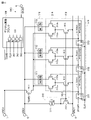
- FIG. 2 is a circuit diagram showing a specific configuration example of the semiconductor integrated circuit of FIG. 1
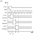
- FIG. 3 is a timing diagram showing the operation of the sequential circuit of FIG. 2
- FIG. 2 is a diagram showing a schematic configuration of a modified example of the semiconductor integrated circuit of FIG. 1
- FIG. 5 is a circuit diagram showing a specific configuration example of the semiconductor integrated circuit of FIG. 4
- FIG. 2 is a block diagram showing a schematic configuration of a semiconductor integrated circuit according to a second embodiment
- FIG. 7 is a circuit diagram showing a specific configuration example of the semiconductor integrated circuit of FIG. 6
- FIG. 8 is a timing diagram showing the operation of the sequential circuit of FIG. 7
- FIG. 3 is a block diagram showing a schematic configuration of a semiconductor integrated circuit according to a third embodiment
- FIG. 10 is a circuit diagram showing a specific configuration example of the semiconductor integrated circuit of FIG. 9
- FIG. 11 is a timing diagram showing the operation of the logic circuit of FIG. 10
- FIG. 1 is a circuit diagram showing a configuration example of a current measurement circuit connected to a power supply node of a semiconductor integrated circuit
- FIG. 11 is a circuit diagram showing a configuration example of a semiconductor integrated circuit according to a fourth embodiment
- FIG. 12 is a circuit diagram showing a configuration example of a current measurement circuit connected to a power supply node of a semiconductor integrated circuit in the semiconductor device of the fifth embodiment
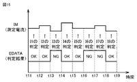
- 15 is a diagram for explaining error data in FIG. 14
- FIG. FIG. 11 is a circuit diagram showing a configuration example of a semiconductor integrated circuit 10 according to a fifth embodiment
- FIG. 17 is a timing chart showing a procedure for transferring error data to D flip-flops forming the second switch group in FIG
- FIG. 1 is a block diagram showing a schematic configuration of a semiconductor integrated circuit according to Embodiment 1.
- a semiconductor integrated circuit 10 includes an analog circuit block 1, a switch group 2, a current source control circuit 3, a current source group 4, a sequential circuit 5, and a power supply node (node) 6. , 7 and a ground node 8 .
- Analog circuit block 1 is an analog circuit that operates with power supply voltage VDD1 applied between power supply node 6 and ground node 8 .
- the current source group 4 includes a plurality of current sources 40.
- FIG. 1 representatively shows four current sources 40, but the number of current sources 40 is not limited to four.
- the magnitude of the current generated by each of the multiple current sources 40 is controlled by the bias voltage Vb1 supplied from the current source control circuit 3.
- FIG. A first end 40 a of each of the plurality of current sources 40 is connected to the ground node 8 , and a second end 40 b of each is connected to the analog circuit block 1 via the switch group 2 .
- a plurality of current sources 40 function as current sinks for the analog circuit block 1 .
- the switch group 2 includes a large number of switches.
- the switch group 2 electrically connects the second end 40b of each current source 40 constituting the current source group 4 to the analog circuit block 1 in the normal mode.
- the switch group 2 individually and selectively switches the electrical connection of the second ends 40b of the plurality of current sources 40 constituting the current source group 4 from the analog circuit block 1 to the power supply node 7 in the test mode. Thereby, the current flowing through each current source 40 constituting the current source group 4 can be individually measured from the outside of the semiconductor integrated circuit 10 via the power supply node 7 .
- the switch group 2 includes two switches 20 a and 20 b corresponding to each current source 40 .
- a second end 40b of each current source 40 is connected to the power supply node 7 through a corresponding switch 20a and to the analog circuit block 1 through a corresponding switch 20b.
- the sequential circuit 5 controls the switch group 2 in response to the control signal.
- the sequential circuit 5 is a synchronous sequential circuit that operates in synchronization with the clock signal CLK.
- Sequential circuit 5 sequentially connects second ends 40b of a plurality of current sources 40 constituting current source group 4 one by one to power supply node 7 in response to a control signal (eg, test start pulse START) in the test mode. electrically connected to the As a result, the current flowing through each of the plurality of current sources 40 forming the current source group 4 can be sequentially measured one by one from the outside of the semiconductor integrated circuit 10 via the power supply node 7 .
- FIG. 2 is a circuit diagram showing a specific configuration example of the semiconductor integrated circuit of FIG.
- FIG. 2 shows a specific configuration example of the current source group 4, current source control circuit 3, switch group 2, and sequential circuit 5 in FIG.
- the analog circuit block 1 is divided into actual circuits 101, 102 and 103 in association with the current source NMOS transistors 401, 402 and 403, respectively.
- the current source group 4 includes multiple NMOS (Negative-channel Metal Oxide Semiconductor) transistors 401 , 402 , 403 as multiple current sources 40 .
- the source of each of NMOS transistors 401 - 403 is connected to ground node 8 as first end 40 a of current source 40 .
- Each of the NMOS transistors 401-403 functions as a current sink that absorbs current through its drain (corresponding to the second end 40b of the current source 40).
- FIG. 2 representatively shows three current source NMOS transistors 401 to 403, the number of power supply NMOS transistors 401 to 403 is not limited to three.
- transistors instead of the above MOS transistors, other types of transistors such as bipolar transistors may be used. Similarly, in other circuits of the present disclosure, the types of transistors are not particularly limited.
- the current source control circuit 3 includes a reference current source 301 connected in series between the power supply node 6 and the ground node 8, and an NMOS transistor 302 as a reference transistor.
- the source of NMOS transistor 302 is connected to ground node 8 .
- a current I is input from the reference current source 301 to the drain of the NMOS transistor 302 .
- the gate and drain of the NMOS transistor 302 are connected together. That is, the NMOS transistor 302 is diode-connected. As a result, a voltage corresponding to the current I of the reference current source 301 is generated between the gate and source of the NMOS transistor 302 . Further, the gate of NMOS transistor 302 is connected to each gate of NMOS transistors 401-403 forming current source group 4, and the source of NMOS transistor 302 is connected to each source of NMOS transistors 401-403. Therefore, the gate-source voltage of each of NMOS transistors 401 - 403 is equal to the gate-source voltage of NMOS transistor 302 . As a result, the NMOS transistor 302 and the NMOS transistors 401 to 403 form a so-called current mirror. Current source control circuit 3 supplies bias voltage Vb1 to the gates of NMOS transistors 401-403.
- the switch group 2 includes a plurality of sets of switch NMOS transistors (201a, 201b) to (203a, 203b) corresponding to the plurality of NMOS transistors 401 to 403 constituting the current source group 4, respectively.
- NMOS transistors 201a and 201b correspond to switches 20a and 20b in FIG. 1, respectively.
- Each source of the NMOS transistors 201a and 201b is connected to the drain of the corresponding NMOS transistor 401 (that is, the second end 40b of the corresponding current source 40).
- the drain of NMOS transistor 201 a is connected to power supply node 7 .
- the drain of the NMOS transistor 201b is connected to the real circuit 101 forming the analog circuit block 1.
- FIG. A gate control signal for controlling on/off of the NMOS transistors 201a and 201b is input from the sequential circuit 5 to each gate of the NMOS transistors 201a and 201b.
- the sequential circuit 5 includes a plurality of cascaded D flip-flops 501 to 503 and has a circuit configuration similar to that of a shift register.
- D flip-flops 501-503 correspond to NMOS transistors 401-403 used as current sources, respectively.
- Each of the D flip-flops 501 to 503 has switch NMOS transistors (201a, 201b) to (203a) connected to the corresponding current source NMOS transistors according to the internal state (that is, set state or reset state). , 203b).
- the sequential circuit 5 includes N first to Nth D flip-flops corresponding to NMOS transistors for N current sources from the first to Nth. is provided.
- the N D flip-flops are cascaded. That is, the output terminal (Q terminal) of the i-th (1 ⁇ i ⁇ N-1) D flip-flop is connected to the input terminal (D terminal) of the (i+1)-th D flip-flop.
- the drains of the N current source NMOS transistors are connected to the sources of the first and second switch NMOS transistors. As a result, the drain of each NMOS transistor for current source is connected to the power supply node 7 via the first NMOS transistor for switch, and is connected to the analog circuit block 1 via the second NMOS transistor for switch. Connected.
- each of the N D flip-flops is connected to the gate of a first NMOS transistor for switching which is connected to the corresponding NMOS transistor for current source.
- the inverting output terminal (QB terminal) of each of the N D flip-flops is connected to the gate of the second NMOS transistor for switching which is connected to the corresponding NMOS transistor for current source.
- the test start pulse STRAT when the test start pulse STRAT is input to the D terminal of the first D flip-flop, the first D flip-flop is set. After that, in synchronization with the clock signal, the test start pulse STRAT is sequentially transferred from the first D flip-flop to the N-th D flip-flop. That is, the N D flip-flops are sequentially changed from the reset state to the set state one by one, and then return to the reset state.
- the j-th (1 ⁇ j ⁇ N) D flip-flop is in the set state, the first NMOS transistor for switch connected to the corresponding j-th NMOS transistor for current source is in the conductive state (on).
- the second NMOS transistor is in a non-conducting state (also referred to as an off state).
- the source of the j-th current source NMOS transistor and the power supply node 7 become conductive, so that the current flowing through the j-th current source NMOS transistor is transferred via the power supply node 7. It can be measured from the outside of the semiconductor integrated circuit 10 .
- FIG. 3 is a timing diagram showing the operation of the sequential circuit of FIG. The operation of the sequential circuit 5 will be described below with reference to FIGS. 2 and 3.
- a test start pulse STRAT is input to the D terminal of the D flip-flop 501 from time t1 to time t3 in FIG.
- the test start pulse STRAT is input at a timing including one falling edge of the clock signal CLK.
- the input to the D terminal of the D flip-flop 501 is at a high level, so the D flip-flop 501 switches to the set state.
- the output signal FF1OUT of the Q terminal of the D flip-flop 501 switches to high level, and the output signal FF1OUTB of the QB terminal of the D flip-flop 501 switches to low level.
- the output of the QB terminal is the inverted output of the Q terminal.
- the drain of NMOS transistor 401 is electrically connected to power supply node 7 through conductive NMOS transistor 201a.
- the input to the D terminal of the D flip-flop 502 is at high level, so the internal state of the D flip-flop 502 switches to the set state.
- the output signal FF2OUT of the Q terminal of the D flip-flop 502 switches to high level, and the output signal FF2OUTB of the QB terminal of the D flip-flop 502 switches to low level.
- the drain of NMOS transistor 402 is electrically connected to power supply node 7 through conductive NMOS transistor 202a.
- the D flip-flops 501 to 503 are switched to high level one by one in order.
- the electrical connections of the drains of the current source NMOS transistors 401 to 403 (that is, the second ends 40b of the plurality of current sources 40) are sequentially switched from the analog circuit block 1 to the power supply node 7 one by one. , and then switch to the analog circuit block 1 again.
- the current flowing through each of NMOS transistors 401 to 403 can be sequentially measured from the outside of semiconductor integrated circuit 10 via power supply node 7 .
- the timing of current measurement it is conceivable to consider the settling time of the current signal and measure it, for example, at the timing of the rising edge of the clock signal CLK. Furthermore, in order to reduce the error due to noise, the average value of the current signal during the high level period of the clock signal CLK may be calculated.
- the magnitude of the current generated by each current source 40 can be sequentially controlled without complicated control. Moreover, by increasing the frequency of the clock signal CLK, the measurement can be performed at a higher speed. In this case, it is necessary to determine the frequency of the clock signal CLK so as to obtain the necessary measurement accuracy in consideration of settling time and errors due to noise.
- FIG. 4 is a diagram showing a schematic configuration of a modified example of the semiconductor integrated circuit of FIG.
- the semiconductor integrated circuit 10A of FIG. 4 includes an analog circuit block 1, a switch group 2, a current source control circuit 3, a current source group 4, a sequential circuit 5, a power It has a node 6 and ground nodes 8 and 9 .
- Analog circuit block 1 is an analog circuit that operates with power supply voltage VDD1 applied between power supply node 6 and ground node 8 .
- the current source group 4 includes a plurality of current sources 40.
- a plurality of current sources 40 are controlled by a bias voltage Vb1 supplied from the current source control circuit 3 .
- a first end 40 a of each current source 40 is connected to the power supply node 6 , and a second end 40 b of each is connected to the analog circuit block 1 via the switch group 2 .
- a plurality of current sources 40 function as current sources for the analog circuit block 1 .
- the switch group 2 includes a large number of switches.
- the switch group 2 connects the second end 40b of each of the plurality of current sources 40 forming the current source group 4 to the analog circuit block 1 in the normal mode.
- the switch group 2 individually switches the electrical connection of the second end 40b of each of the plurality of current sources 40 constituting the current source group 4 from the analog circuit block 1 to the ground node 9 in the test mode. Thereby, the current flowing through each current source 40 constituting the current source group 4 can be individually measured from the outside of the semiconductor integrated circuit 10A through the ground node 9 .
- the sequential circuit 5 controls the switch group 2 in response to the control signal.
- the sequential circuit 5 is a synchronous sequential circuit that operates in synchronization with the clock signal CLK.
- the sequential circuit 5 sequentially connects the second ends 40b of the plurality of current sources 40 constituting the current source group 4 one by one to the ground node 9 in response to a control signal (for example, a test start pulse START) in the test mode. electrically connected to the As a result, currents flowing through the plurality of current sources 40 forming the current source group 4 can be sequentially measured one by one from the outside of the semiconductor integrated circuit 10 via the ground node 9 .
- FIG. 5 is a circuit diagram showing a specific configuration example of the semiconductor integrated circuit of FIG.
- the circuit diagram of FIG. 5 corresponds to the circuit diagram of FIG. 2, and the NMOS transistors of FIG. 2 are replaced with PMOS (Positive Metal Oxide Semiconductor) transistors.
- PMOS Platinum Oxide Semiconductor
- the current source group 4 includes a plurality of PMOS transistors 401b, 402b, 403b. Each source of PMOS transistors 401b-403b is connected to power supply node 6. FIG. Each of the PMOS transistors 401b-403b functions as a current source supplying current from the drain.
- the current source control circuit 3 includes a PMOS transistor 302b as a reference transistor connected in series between the power supply node 6 and the ground node 8, and a reference current source 301b.
- the source of PMOS transistor 302 b is connected to power supply node 6 .
- a current I flows from the drain of the PMOS transistor 302b to the reference current source 301b.
- the PMOS transistor 302b is a so-called diode-connected transistor in which the gate and the drain are connected. By connecting the gate of the PMOS transistor 302b to the gates of the PMOS transistors 401b to 403b forming the current source group 4, these PMOS transistors form a current mirror. PMOS transistor 302b supplies bias voltage Vb1 to the gates of PMOS transistors 401b-403b.
- the switch group 2 includes a plurality of sets of switch PMOS transistors (201c, 201d) to (203c, 203b) corresponding to the plurality of PMOS transistors 401b to 403b constituting the current source group 4, respectively.
- Each source of the PMOS transistors 201c and 201d is connected to the drain of the corresponding PMOS transistor 401b (that is, the second end 40b of the corresponding current source 40).
- the drain of PMOS transistor 201 c is connected to ground node 9 .
- the drain of the PMOS transistor 201 d is connected to the real circuit 101 forming the analog circuit block 1 .
- a gate control signal for controlling on/off of the PMOS transistors 201c and 201d is input from the sequential circuit 5 to each gate of the PMOS transistors 201c and 201d. The same applies to PMOS transistors 202c, 202d and PMOS transistors 203c, 203d.
- the sequential circuit 5 includes cascaded D flip-flops 501-503 corresponding to PMOS transistors 401b-403b, respectively, as in FIG.
- the Q terminal of D flip-flop 501 is connected to the gate of PMOS transistor 201d
- the QB terminal of D flip-flop 501 is connected to the gate of PMOS transistor 201c.
- the sequential circuit 5 operates in the same manner as in FIG. 3 based on the test start pulse STRAT and the clock signal CLK.
- the electrical connection of the drains of the current source PMOS transistors 401b to 403b (that is, the second ends 40b of the plurality of current sources 40) is switched from the analog circuit block 1 to the ground node 9 one by one in order. , and then switch to the analog circuit block 1 again.
- the semiconductor integrated circuit 10 of the first embodiment includes the first analog circuit block 1, the plurality of current sources 40 functioning as current sinks for the first analog circuit block 1, the first switch group 2, and the It has a first node (power node 6), a second node (power node 7), and a third node (ground node 8).
- the first analog circuit block 1 operates with a voltage VDD1 applied between a first node (power supply node 6) and a third node (ground node 8).
- a first end 40a of each of the plurality of first current sources 40 is connected to a third node (ground node 8), and a second end 40b of each is connected to the first analog circuit block 1 via the first switch group 2. be done.
- the first switch group 2 is provided between the plurality of first current sources 40 and the first analog circuit block 1, and electrically connects the second ends 40b of the plurality of first current sources 40 in the test mode.
- the first analog circuit block 1 is individually switched to the second node (power supply node 7). According to the above configuration, the current flowing through each of the plurality of first current sources 40 in the test mode can be individually measured from the outside of semiconductor integrated circuit 10 via the second node (power supply node 7).
- the semiconductor integrated circuit 10A of the modification of the first embodiment includes a first analog circuit block 1, a plurality of current sources 40 functioning as current sources for the first analog circuit block 1, a first switch group 2, It has a first node (ground node 8), a second node (ground node 9), and a third node (power supply node 6).
- the first analog circuit block 1 operates with a voltage VDD1 applied between a first node (ground node 8) and a third node (power node 6).
- a first end 40a of each of the plurality of first current sources 40 is connected to a third node (power supply node 6), and a second end 40b of each is connected to the first analog circuit block 1 via the first switch group 2. be done.
- the first switch group 2 is provided between the plurality of first current sources 40 and the first analog circuit block 1, and electrically connects the second ends 40b of the plurality of first current sources 40 in the test mode.
- the first analog circuit block 1 is individually switched to the second node (ground node 9). According to the above configuration, the current flowing through each of the plurality of first current sources 40 in the test mode can be individually measured from the outside of the semiconductor integrated circuit 10 through the second node (ground node 9).
- the configuration of the semiconductor integrated circuit 10 described above and the semiconductor integrated circuit 10A of the modified example may be combined.
- the current of each current source 40 functioning as a current sink can be measured from the outside of the semiconductor integrated circuit (10, 10A) through the power supply node 7 different from the power supply node 6 for the analog circuit block 1.
- the current of each current source 40 functioning as a current source can be individually measured from the outside of the semiconductor integrated circuit 10 through a ground node 9 different from the ground node 8 for the analog circuit block 1 .
- the semiconductor integrated circuits 10 and 10A of the first embodiment further include a sequential circuit 5 that controls the first switch group 2 described above.
- Sequential circuit 5 includes a plurality of cascaded D flip-flops 501 - 503 corresponding to a plurality of current sources 40 forming current source group 4 .
- Each D flip-flop controls the switch group 2 to electrically connect the corresponding current source 40 to the second node (power supply node 7/ground node 9) in the set state.
- the sequential circuit 5 configured as described above, the current value generated by each current source 40 can be measured at high speed with simple control.
- semiconductor integrated circuit 10B includes two analog circuit blocks 110 and 120, and these analog circuit blocks 110 and 120 have different power supply voltages.
- the power supply node 6 for one analog circuit block 110 and the power supply node 7 for the other analog circuit block 120 are different, when measuring the current source 40 for one analog circuit block 110, Power supply node 7 for the other analog circuit block 120 can be used.
- the first end 40 a of the current source 40 functioning as a current sink is connected to the ground node 8 and the second end 40 b is connected to the analog circuit block 110 . Therefore, by switching the electrical connection of the second end 40b of the current source 40 from the analog circuit block 110 to the power supply node 7 for the other analog circuit block 120, the current flowing through each current source 40 can be individually measured.
- a current source 40 functioning as a current source has a first end 40 a connected to the power supply node 6 and a second end 40 b connected to the analog circuit block 110 . Therefore, by switching the electrical connection of the second end 40b of the current source 40 from the analog circuit block 110 to the ground node 9 for the other analog circuit block 120, the current flowing through each current source 40 can be individually measured.
- each current source 40 is a current sink as described with reference to FIGS. 1 and 2 will be described below. Even when each current source 40 described with reference to FIGS. 4 and 5 is a current source, the current flowing through each current source 40 can be measured in a similar manner. In the following description, description of portions corresponding to FIGS. 1 and 2 of Embodiment 1 may not be repeated.
- FIG. 6 is a block diagram showing a schematic configuration of a semiconductor integrated circuit according to the second embodiment.
- semiconductor integrated circuit 10B includes analog circuit blocks (A, B) 110, 120, switch groups 210, 220, current source control circuits 310, 320, current source groups 410, 420, It comprises sequential circuits 510 and 520 , power supply nodes 6 and 7 , ground nodes 8 and 9 , and test mode switches 910 and 920 .
- the power supply node 6 is supplied with the power supply voltage VDD1, and the power supply node 7 is supplied with the power supply voltage VDD2.
- Ground node 8 is supplied with reference potential GND1, and ground node 9 is supplied with reference potential GND2.
- Analog circuit block 110 operates with power supply voltage VDD1 applied between power supply node 6 and ground node 8 .
- Analog circuit block 120 operates with power supply voltage VDD2 applied between power supply node 7 and ground node 9 .
- Ground node 8 and ground node 9 may be common.
- Analog circuit block 110, switch group 210, current source control circuit 310, current source group 410, and sequential circuit 510 correspond to analog circuit block 1, switch group 2, current source control circuit 3, current source group 4, and They correspond to the sequential circuits 5, respectively.
- a test mode switch 910 is provided between the switch group 210 and the power supply node 7 .
- the second end 40 b of each current source 40 constituting the current source group 410 is electrically connected to the analog circuit block 110 via the switch group 210 .
- the test mode for measuring the current of each current source 40 of the current source group 410 the second end 40b of each current source 40 constituting the current source group 410 is connected to the power supply node through the switch group 210 and the test mode switch 910. 7 are individually electrically connected.
- the test mode switch 910 is controlled to be in a conducting state (on state) during the test mode of the current source group 410, and is controlled to be in a non-conducting state (off state) during the normal mode.
- a conducting state on state
- a non-conducting state off state
- the sequential circuit 510 sets the second ends 40b of the plurality of current sources 40 forming the current source group 410 to 1 based on control signals (clock signal CLK, test start pulse STRAT). are electrically connected to the power supply node 7 one by one. This makes it possible to individually measure the current flowing through each current source 40 forming the current source group 410 in the test mode of the current source group 410 .
- Analog circuit block 120, switch group 220, current source control circuit 320, current source group 420, and sequential circuit 520 are also analog circuit block 1, switch group 2, current source control circuit 3, current source group 4, and They correspond to the sequential circuits 5, respectively. These circuits in FIG. 5 are connected to power supply node 7 and ground node 9 instead of power supply node 6 and ground node 8 described above.
- Switch group 220 includes two switches 21 a and 21 b corresponding to each current source 41 . A second end 41b of each current source 41 is connected to the power supply node 7 via the corresponding switch 21a and to the analog circuit block 1 via the corresponding switch 21b.
- a test mode switch 920 is provided between the switch group 220 and the power supply node 6 . As with the test mode switch 910, the test mode switch 920 is controlled to be in a conducting state (on state) in the test mode for measuring the current of each current source 41 of the current source group 420, and in a non-conducting state (to be turned off) in the normal mode. off state). In the normal mode, the second end 41 b of each current source 41 constituting the current source group 420 is electrically connected to the analog circuit block 120 via the switch group 220 .
- each current source 41 of the current source group 420 In the test mode in which the current of each current source 41 of the current source group 420 is measured, the second end 41b of each current source 41 constituting the current source group 420 is connected to the power node through the switch group 220 and the test mode switch 920. 6 are individually electrically connected.
- the sequential circuit 520 sets the second ends 41b of the plurality of current sources 41 forming the current source group 420 to 1 based on the control signals (clock signal CLK2, test start pulse STRAT2). are connected to the power supply node 7 one by one. Thereby, the current flowing through each current source 41 constituting the current source group 420 can be individually measured in the test mode.
- the semiconductor integrated circuit 10B of FIG. 6 further differs from the semiconductor integrated circuit 10 of FIG. 1 in that current control signals ION_A and ION_B are input to current source control circuits 310 and 320, respectively.
- the current source control circuit 310 responds to the current control signal ION_A to set the current flowing through each current source 40 constituting the current source group 410 to zero in the test mode in which the current of each current source 41 of the current source group 420 is measured. to or reduce. This can prevent the current source group 410 from affecting the current measurement of each current source 41 .
- the current source control circuit 320 responds to the current control signal ION_B in the test mode in which the current of each current source 40 of the current source group 410 is measured. Zero or reduce the current. This allows the current source group 420 to suppress the influence of each current source 40 on the current measurement.
- FIG. 7 is a circuit diagram showing a specific configuration example of the semiconductor integrated circuit of FIG. 7 shows a specific configuration example of the current source group 410, current source control circuit 310, switch group 210, analog circuit block 110, sequential circuit 510, and test mode switch 910 in FIG. Also, a specific configuration example of the current source group 420, the current source control circuit 320, and the test mode switch 920 of FIG. 6 is simply shown.
- analog circuit block 110, current source group 410, switch group 210, and sequential circuit 510 have configurations similar to those of analog circuit block 1, current source group 4, switch group 2, and sequential circuit shown in FIG. 5 is the same as the configuration.
- the real circuits 111 to 113 forming the analog circuit block 110 correspond to the real circuits 101 to 103 in FIG. 2, respectively.
- NMOS transistors 411 to 413 forming current source group 410 correspond to NMOS transistors 401 to 403 in FIG.
- the NMOS transistors 211a, 211b-213a, 213b forming the switch group 210 correspond to the NMOS transistors 201a, 201b-203a, 203b in FIG. 2, respectively.
- D flip-flops 511-513 forming sequential circuit 510 correspond to D flip-flops 501-503 in FIG. 2, respectively. Therefore, the connection of these elements will not be repeated.
- the current source control circuit 310 includes NMOS transistors 312 and 316, a PMOS transistor 315, and a constant voltage source 317.
- PMOS transistor 315, NMOS transistor 316 and NMOS transistor 312 are connected in series between power supply node 6 and ground node 8 in this order.
- the constant voltage source 317 is, for example, a bandgap reference voltage generation circuit, and is adjusted so as to reduce temperature dependence.
- a constant voltage source 317 is connected between the source and gate of the PMOS transistor 315 .
- Constant voltage source 317 and PMOS transistor 315 constitute reference current source 311 .
- the NMOS transistor 312 is a so-called diode-connected transistor whose gate and drain are connected.
- the gate of NMOS transistor 312 is connected to the gates of NMOS transistors 411 to 413 forming current source group 410 .
- the NMOS transistors 312, 411-413 form a current mirror.
- a current control signal ION_A is input to the gate of the NMOS transistor 316 .
- the current control signal ION_A is controlled to high level so that the NMOS transistor 316 becomes conductive.
- the NMOS transistor 316 is rendered non-conductive by controlling the current control signal ION_A to a low level. This suppresses the influence of each current source 41 of the current source group 420 on the current measurement.
- a PMOS transistor 911 is provided as the test mode switch 910 in FIG.
- the source of PMOS transistor 911 is connected to power supply node 7 .
- the drain of the PMOS transistor 911 is connected to the drains of the PMOS transistors 211 a , 212 a , 213 a that form the switch group 210 .
- the control signal TSWB supplied to the gate of the PMOS transistor 911 is controlled to high level in the normal mode, and controlled to low level in the test mode of the current source group 410 .
- the PMOS transistor 911 becomes non-conductive in the normal mode, and becomes conductive in the test mode of the current source group 410 .
- NMOS transistor 421 forming current source group 420 corresponds to NMOS transistor 411 .
- NMOS transistors 322 and 326, PMOS transistor 325 and constant voltage source 327 forming current source control circuit 320 correspond to NMOS transistors 312 and 316, PMOS transistor 315 and constant voltage source 317, respectively. Therefore, the description of these elements will not be repeated.
- a PMOS transistor 921 is provided as the test mode switch 920 in FIG.
- the source of PMOS transistor 921 is connected to power supply node 6 .
- the drain of PMOS transistor 921 is connected to switch group 220 .
- a control signal TSWA supplied to the gate of the PMOS transistor 921 is controlled to high level in the normal mode, and controlled to low level in the test mode of the current source group 420 .
- the PMOS transistor 921 becomes non-conductive in the normal mode, and becomes conductive in the test mode of the current source group 420 .
- FIG. 8 is a timing diagram showing the operation of the sequential circuit of FIG.
- FIG. 8 shows the operation of the sequential circuit 510 when measuring the current flowing through the NMOS transistors 411 to 413 for the current sources forming the current source group 410 of FIG.
- each of D flip-flops 511-513 changes its internal state at the fall of clock signal CLK.
- control signal TSWA and current control signal ION_A are fixed at high level. Therefore, PMOS transistor 921 is controlled to be non-conductive and NMOS transistor 316 is controlled to be conductive.
- a test start pulse STRAT is input to the D terminal of the D flip-flop 511 from time t1 to time t3.
- the control signal TSWB and the current control signal ION_B are switched to low level.
- PMOS transistor 911 between switch group 210 and power supply node 7 is controlled to be conductive.
- the NMOS transistor 326 is controlled to be non-conductive, the current flowing through the NMOS transistors (such as 421) for each current source forming the current source group 420 becomes zero.
- the clock signal CLK further falls.
- the input to the D terminal of the D flip-flop 511 is at a high level, so the D flip-flop 511 switches to the set state.
- the output signal FF1OUT of the Q terminal of the D flip-flop 511 switches to high level, and the output signal FF1OUTB of the QB terminal of the D flip-flop 511 switches to low level.
- the drain of NMOS transistor 411 is electrically connected to power supply node 7 .
- the input to the D terminal of the D flip-flop 512 is at high level, so the internal state of the D flip-flop 512 switches to the set state.
- the output signal FF2OUT of the Q terminal of the D flip-flop 512 switches to high level, and the output signal FF2OUTB of the QB terminal of the D flip-flop 512 switches to low level.
- the drain of NMOS transistor 412 is electrically connected to power supply node 7 .
- the D flip-flops 511 to 513 are switched to high level one by one in order.
- the connections of the drains of the current source NMOS transistors 411 to 413 (that is, the second ends 40b of the plurality of current sources 40) are switched one by one in order from the analog circuit block 110 to the power supply node 7. It switches to the analog circuit block 110 again.
- the current flowing through each of the NMOS transistors 411 to 413 can be measured one by one.
- the current source 41 for the other analog circuit block 120 does not have to be set to zero, and the current may be set to be smaller than the measured current for the current source 40 to be measured. In this case, if the offset by the current source 41 is taken into account, it is possible to suppress the decrease in current measurement accuracy.
- the semiconductor integrated circuit 10C includes an analog circuit block 110 and a digital circuit block 130, that is, a mixed signal circuit in which a digital circuit and an analog circuit are mixed.
- power supply node 6 for analog circuit block 110 and power supply node 7 for digital circuit block 130 are separated for avoidance of digital noise and difference in operating power supply voltage.
- the power supply node 7 for the digital circuit block 130 can be used as a current measurement terminal.
- the first end 40 a of the current source 40 functioning as a current sink is connected to the ground node 8 and the second end 40 b is connected to the analog circuit block 110 . Therefore, by switching the electrical connection of the second end 40b of the current source 40 from the analog circuit block 110 to the power supply node 7 for the digital circuit block 130, the current flowing through each current source 40 can be individually measured.
- a current source 40 functioning as a current source has a first end 40 a connected to the power supply node 6 and a second end 40 b connected to the analog circuit block 110 . Therefore, by switching the electrical connection of the second end 40b of the current source 40 from the analog circuit block 110 to the ground node 9 for the digital circuit block 130, the current flowing through each current source 40 can be measured individually.
- each current source 40 is a current sink as described with reference to FIGS. 1 and 2 will be described below. Even when each current source 40 described with reference to FIGS. 4 and 5 is a current source, the current flowing through each current source 40 can be measured in a similar manner. 1 and 2 of the first embodiment and FIGS. 6 and 7 of the second embodiment will not be described repeatedly.
- FIG. 9 is a block diagram showing a schematic configuration of a semiconductor integrated circuit according to the third embodiment.
- semiconductor integrated circuit 10C includes analog circuit block 110, digital circuit block 130, switch group 210, current source control circuit 310, current source group 410, sequential circuit 510, and a power supply node. 6, 7, ground nodes 8, 9, and a test mode switch 910.
- the power supply node 6 is supplied with the power supply voltage VDD1, and the power supply node 7 is supplied with the power supply voltage VDD2.
- Ground node 8 is supplied with reference potential GND1, and ground node 9 is supplied with reference potential GND2.
- Analog circuit block 110 operates with power supply voltage VDD1 applied between power supply node 6 and ground node 8 .
- the analog circuit block 110, switch group 210, current source group 410, sequential circuit 510, and test mode switch 910 in FIG. 9 are the same as in FIG.
- the current source control circuit 310 differs from the case of FIG. 6 in that it does not have a current control function based on the current control signal ION_A. This is because there is no need to measure the current flowing through the current source provided in the digital circuit block 130 .
- the digital circuit block 130 operates with the power supply voltage VDD2 applied between the power supply node 7 and the ground node 9.
- a clock signal CLK and digital input signals IN1, IN2, . . . , INN are input to the digital circuit block 130, for example.
- FIG. 10 is a circuit diagram showing a specific configuration example of the semiconductor integrated circuit of FIG.
- FIG. 10 shows a specific configuration example of the current source group 410, current source control circuit 310, switch group 210, analog circuit block 110, sequential circuit 510, and test mode switch 910 in FIG.
- a configuration example of the input interface 131 of the digital circuit block 130 is also shown.
- the current source control circuit 310 in FIG. 10 differs from the current source control circuit 310 in FIG. 7 in that the NMOS transistor 316 is not provided. This is because there is no need to measure the current flowing through the current sources provided in the digital circuit block 130, so there is no need to set the current flowing through the current source group 410 to zero.
- the input interface 131 of the digital circuit block 130 includes a plurality of AND gates for calculating the logical product of the input signal of the digital circuit block 130 (clock signal CLK, digital input signals IN1, IN2, . . . , as an example) and the control signal TSWB. .
- control signal TSWB is controlled to high level. Thereby, each input signal of the digital circuit block 130 is input to the internal circuit of the digital circuit block 130 as it is. Also, the PMOS transistor 911 forming the test mode switch 910 is controlled to be in a non-conducting state.
- the control signal TSWB is controlled to low level.
- each input signal of the digital circuit block 130 is fixed to a low level by AND operation with the control signal TSWB.
- the power consumption in the digital circuit block 130 becomes zero, so that the current measurement of the NMOS transistors 411-413 for each current source is not affected.
- the method of fixing the logic level of each input signal of the digital circuit block 130 is not limited to this method.
- the PMOS transistor 911 forming the test mode switch 910 is controlled to be in a conducting state. Thereby, the current flowing through the NMOS transistors 411 to 413 for each current source through the power supply node 7 can be measured.
- FIG. 11 is a timing diagram showing the operation of the logic circuit of FIG. FIG. 11 shows the operation of the sequential circuit 510 when measuring the currents flowing through the current source NMOS transistors 411 to 413 constituting the current source group 410 of FIG.
- each of D flip-flops 511-513 changes its internal state at the fall of clock signal CLK.
- a test start pulse STRAT is input to the D terminal of the D flip-flop 511 from time t1 to time t3.
- the control signal TSWB is switched to low level.
- PMOS transistor 911 between switch group 210 and power supply node 7 is controlled to be conductive.
- each input signal of the digital circuit block 130 is fixed at low level. As a result, the power consumption of the digital circuit block 130 becomes zero.
- Embodiment 4 shows a specific example of current measuring circuit 16 connected to power supply node 7 of semiconductor integrated circuit 10D. Furthermore, a case where a plurality of spare current sources are provided in current source group 410 and all of the plurality of current sources are switched to the plurality of spare current sources based on the measurement result of current measuring circuit 16 will be described. Although a case where the semiconductor integrated circuit 10D is provided with the analog circuit block 110 and the digital circuit block 130 will be described below, the technology of the present embodiment is applicable to the case where the semiconductor integrated circuit 10D is provided with a plurality of analog circuit blocks. The same applies if there is
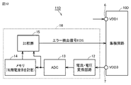
- FIG. 12 is a circuit diagram showing a configuration example of a current measurement circuit connected to a power supply node of a semiconductor integrated circuit.
- FIG. 12 shows an example in which the semiconductor device 11E is configured by the separate semiconductor integrated circuit 10D and the current measurement circuit 16, but the current measurement circuit 16 is included inside the semiconductor integrated circuit 10D. good too.
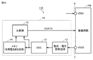
- the current measurement circuit 16 includes a current/voltage conversion circuit 12, an analog-to-digital converter (ADC) 13, a memory 14, and a comparator 15.
- ADC analog-to-digital converter
- the current/voltage conversion circuit 12 takes in the current flowing through the current source connected to the power supply node 7 in the test mode and converts the taken current into voltage.
- the analog-to-digital converter 13 converts the voltage value obtained by current-voltage conversion by the current-voltage conversion circuit 12 into a digital value. As a result, the current value flowing through the current source is digitally converted.
- a memory 14 stores the digitally converted current value.
- Comparator 15 compares the digitally converted current value with the initial current value stored in memory 14 .
- the comparator 15 activates the error detection signal EDS (for example, changes it to high level) when the absolute value of the difference between the current value at the present time and the initial current value exceeds the threshold.
- the error detection signal EDS is input to the semiconductor integrated circuit 10D. Note that once the error detection signal EDS is activated, the active state is maintained.
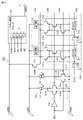
- FIG. 13 is a circuit diagram showing a configuration example of a semiconductor integrated circuit according to the fourth embodiment.
- Semiconductor integrated circuit 10D in FIG. 13 differs from semiconductor integrated circuit 10C in FIG. 10 in the configuration of current source group 410 and current source control circuit 310 .
- Semiconductor integrated circuit 10D in FIG. 13 differs from semiconductor integrated circuit 10C in FIG. 10 in that it further includes an inverter 314 that receives error detection signal EDS.
- the current source group 410 in FIG. 13 further includes NMOS transistors 411a, 412a, . . . connected in parallel to the NMOS transistors 411, 412, .
- current source control circuit 310 of FIG. 13 further includes reference current source 311a and NMOS transistor 312a.
- Reference current source 311 a and NMOS transistor 312 a are connected in series between power supply node 6 and ground node 8 and in parallel with the series connection circuit of reference current source 311 and NMOS transistor 312 .
- the gate of the NMOS transistor 312 is connected to its own drain and to the gates of the NMOS transistors 411, 412, .
- the NMOS transistors 312, 411, 412, . . . form a current mirror.
- the gate of the NMOS transistor 312a is connected to its own drain and to the gates of the NMOS transistors 411a, 412a, .
- NMOS transistors 312a, 411a, 412a, . . . are configured.
- the current source control circuit 310 of FIG. 13 further includes NMOS transistors 313 and 313a connected in parallel with the NMOS transistors 312 and 312a, respectively.
- An error detection signal EDS is input to the gate of the NMOS transistor 313 .
- An error detection signal EDS whose logical value is inverted by an inverter 314 is input to the gate of the NMOS transistor 313a.
- the error detection signal EDS is inactive (that is, low level), so the NMOS transistor 313 is non-conductive and the NMOS transistor 313a is conductive. Therefore, the current I generated by the reference current source 311 flows through the NMOS transistor 312, and this current I is copied and flows through the NMOS transistors 411, 412, . On the other hand, the current I generated by the reference current source 311a flows through the NMOS transistor 313a and does not flow through the NMOS transistor 312a. Therefore, the current I does not flow through the NMOS transistors 411a, 412a, . . .
- the error detection signal EDS becomes active (that is, high level)
- the NMOS transistor 313 becomes conductive and the NMOS transistor 313a becomes non-conductive. Therefore, current I generated by reference current source 311 flows through NMOS transistor 312 a and does not flow through NMOS transistor 312 . As a result, the current I does not flow through the NMOS transistors 411, 412, .
- the current I generated by the reference current source 311a flows through the NMOS transistor 312a, and this current I is copied and flows through the NMOS transistors 411a, 412a, .
- the semiconductor integrated circuit 10D of FIG. 13 the plurality of first current sources 411, 412, . . . and the plurality of second current sources 411a, 412a, .
- a current flows through only one selected according to the error detection signal EDS.
- EDS error detection signal
- Embodiment 5 In the semiconductor integrated circuit 10E of the fifth embodiment, a case where a plurality of backup current sources are provided in the current source group 410 and a failed current source is individually switched to the backup current source will be described. A case where the semiconductor integrated circuit 10E is provided with the analog circuit block 110 and the digital circuit block 130 will be described below. The same applies if there is
- FIG. 14 is a circuit diagram showing a configuration example of a current measuring circuit connected to a power supply node of a semiconductor integrated circuit in the semiconductor device of the fifth embodiment.
- FIG. 14 shows an example in which the semiconductor device 11F is configured by the separate semiconductor integrated circuit 10E and the current measurement circuit 16, but the current measurement circuit 16 is included inside the semiconductor integrated circuit 10E. good too.
- the current measurement circuit 16 of FIG. 14 is different from that of FIG. 12 in that the comparator 15 outputs error data EDATA indicating the error determination result for each current source NMOS transistor instead of the binary error detection signal EDS. It differs from the current measurement circuit 16 .
- Other points in FIG. 14 are the same as in FIG. 12, so the same or corresponding parts may be denoted by the same reference numerals and the description thereof may not be repeated.
- FIG. 15 is a diagram for explaining the error data in FIG. 15, current measuring circuit 16 detects measured current I1 for first current source 40 forming current source group 410 via power supply node 7 between times t11 and t12. It is assumed that the quality judgment result by the comparator 15 is OK (low level, "0"). In addition, the appropriate range of the current value of the current source 40 differs for each current source 40 .
- the current measurement circuit 16 detects the measured current I2 for the second current source 40 that constitutes the current source group 410 via the power supply node 7 . It is assumed that the quality judgment result by the comparator 15 is OK (low level, "0").
- the current measurement circuit 16 detects the measured current I3 for the third current source 40 constituting the current source group 410 via the power supply node 7. It is assumed that the quality judgment result by the comparator 15 is NG (high level, "1").
- the measured currents I4 to I8 for the fourth to eighth current sources 40 forming the current source group 410 are sequentially detected via the power supply node 7 from time t14 to time t19. be.
- the error data EDATA in this case is data "00100110" indicating the first to eighth determination results.
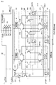
- FIG. 16 is a circuit diagram showing a configuration example of the semiconductor integrated circuit 10 of the fifth embodiment.
- the semiconductor integrated circuit 10E of FIG. 16 differs from the semiconductor integrated circuit 10C of FIG. 10 in the configuration of the current source group 410.
- FIG. 16 differs from the semiconductor integrated circuit 10C of FIG. 10 in that it further includes a switch group 350 and a sequential circuit 330 that controls the switch group 350.
- the current source group 410 in FIG. 16 further includes NMOS transistors 411a, 412a, . . . connected in parallel to the NMOS transistors 411, 412, .
- the switch group 350 is connected between the gates of the NMOS transistors 411, 412, . It includes NMOS transistors 351a, 352a, . Switch group 350 further includes switching NMOS transistors 351b, 352b, . . . connected between the gates of NMOS transistors 411a, 412a, .
- the sequential circuit 330 includes cascaded D flip-flops 331, 332, . . . and has the same configuration as a shift register.
- a clock signal ECLK is input to the CLK terminals of the D flip-flops 331, 332, .
- the D flip-flops 331, 332, . . . correspond to the NMOS transistors 411, 412, . is the opposite direction to the data transfer direction of .
- the sequential circuit 330 includes 1st to Nth N D flip-flops corresponding to the 1st to Nth NMOS transistors for N current sources, respectively.
- a pool is provided.
- the N D flip-flops are cascaded in reverse order. That is, the output terminal (Q terminal) of the i+1-th (1 ⁇ i ⁇ N-1) D flip-flop is connected to the input terminal (D terminal) of the i-th D flip-flop.
- Each of the N current source NMOS transistors is connected in parallel with a spare current source NMOS transistor. Further, a first NMOS transistor for switching is connected between the gate of the NMOS transistor for regular current source and the control line 340 for supplying the bias voltage Vb1.
- a second NMOS transistor for switching is connected between the gate of the NMOS transistor for the backup current source and the control line 340 .
- the Q terminal of each of the N D flip-flops is connected to the gate of a second NMOS transistor for a switch which is connected to a corresponding spare NMOS transistor for a current source.
- the inverted output terminal (QB terminal) of each of the N D flip-flops is connected to the gate of the first NMOS transistor for switching which is connected to the corresponding NMOS transistor for normal current source.
- the error judgment results of the NMOS transistors for the current sources are input to the D terminal of the N-th D flip-flop in order from the first to the N-th, and an N-pulse clock is input.
- the signals are sequentially transferred by the signal ECLK.
- the error judgment results of the first to Nth current source NMOS transistors are held in the first to Nth D flip-flops.
- the j-th (1 ⁇ j ⁇ N) D flip-flop is in the reset state (that is, the corresponding regular current source is normal)
- the first NMOS transistor for the corresponding switch becomes conductive and the second becomes non-conductive.
- the gate of the j-th normal current source NMOS transistor and the control line 340 are brought into a conductive state, so that the j-th normal NMOS transistor is used as a current source.
- the first NMOS transistor for the corresponding switch becomes non-conductive.
- the second NMOS transistor becomes conductive (also referred to as OFF state).
- the gate of the j-th spare NMOS transistor for the current source and the control line 340 become conductive, so the j-th spare NMOS transistor is used as the current source.
- the first D flip-flop 331 is provided to control switch NMOS transistors 351 a and 351 b between the gates of the current source NMOS transistors 411 and 411 a and the control line 340 .
- the Q terminal of the D flip-flop 331 is connected to the gate of the NMOS transistor 351b.
- the QB terminal of D flip-flop 331 is connected to the gate of NMOS transistor 351a.
- a second D flip-flop 332 is provided to control switch NMOS transistors 352 a and 352 b between the gates of the current source NMOS transistors 412 and 412 a and the control line 340 .
- the Q terminal of the D flip-flop 332 is connected to the gate of the NMOS transistor 352b.
- the QB terminal of D flip-flop 332 is connected to the gate of NMOS transistor 352a.
- the Q terminal of the second D flip-flop 332 is connected to the D terminal of the adjacent first D flip-flop 331 .
- the D flip-flops 331, 332, . . . function as a shift register by connecting the D flip-flops 331, 332, .
- FIG. 17 is a timing chart showing the procedure for transferring error data to the D flip-flops forming the second switch group in FIG.
- FIG. 17 shows the procedure for storing the error data EDATA indicating the error determination result shown in FIG. 15 in the D flip-flops 331, 332, .
- FIG. 17 shows the case where the sequential circuit 330 is composed of eight D flip-flops.
- error data EDATA is input to the D terminal of the eighth D flip-flop at eight falling edges of the clock signal ECLK from time t31 to time t38.
- This error data EDATA is sequentially transferred in reverse order to the first D flip-flop 331 by eight falls of the clock signal ECLK3.
- FIG. 17 shows the output signals EFF1 to EFF8 of the Q terminals of eight D flip-flops from the first D flip-flop 331 to the eighth D flip-flop.
- the error determination result (“1”) of the third current source NMOS transistor is input to the D terminal of the eighth D flip-flop. be done.
- This error determination result is transferred to the third D flip-flop by five transfer pulses (clock signal ECLK) from time t34 to time t38.
- clock signal ECLK clock signal
Landscapes
- Physics & Mathematics (AREA)
- Engineering & Computer Science (AREA)
- General Engineering & Computer Science (AREA)
- Computer Hardware Design (AREA)
- Computing Systems (AREA)
- Mathematical Physics (AREA)
- General Physics & Mathematics (AREA)
- Semiconductor Integrated Circuits (AREA)
- Tests Of Electronic Circuits (AREA)
Priority Applications (3)
| Application Number | Priority Date | Filing Date | Title |
|---|---|---|---|
| US18/551,014 US12556168B2 (en) | 2021-04-13 | 2021-04-13 | Semiconductor integrated circuit and semiconductor device |
| JP2023514225A JP7558396B2 (ja) | 2021-04-13 | 2021-04-13 | 半導体集積回路および半導体装置 |
| PCT/JP2021/015331 WO2022219720A1 (ja) | 2021-04-13 | 2021-04-13 | 半導体集積回路および半導体装置 |
Applications Claiming Priority (1)
| Application Number | Priority Date | Filing Date | Title |
|---|---|---|---|
| PCT/JP2021/015331 WO2022219720A1 (ja) | 2021-04-13 | 2021-04-13 | 半導体集積回路および半導体装置 |
Publications (1)
| Publication Number | Publication Date |
|---|---|
| WO2022219720A1 true WO2022219720A1 (ja) | 2022-10-20 |
Family
ID=83639918
Family Applications (1)
| Application Number | Title | Priority Date | Filing Date |
|---|---|---|---|
| PCT/JP2021/015331 Ceased WO2022219720A1 (ja) | 2021-04-13 | 2021-04-13 | 半導体集積回路および半導体装置 |
Country Status (3)
| Country | Link |
|---|---|
| US (1) | US12556168B2 (https=) |
| JP (1) | JP7558396B2 (https=) |
| WO (1) | WO2022219720A1 (https=) |
Citations (6)
| Publication number | Priority date | Publication date | Assignee | Title |
|---|---|---|---|---|
| JPH05288798A (ja) * | 1992-04-14 | 1993-11-02 | Hitachi Ltd | 半導体集積回路およびそのテスト方法 |
| JPH09101347A (ja) * | 1995-10-05 | 1997-04-15 | Mitsubishi Electric Corp | 半導体装置 |
| JP2007078697A (ja) * | 2006-10-23 | 2007-03-29 | Matsushita Electric Ind Co Ltd | 集積回路素子 |
| JP2009513968A (ja) * | 2005-10-26 | 2009-04-02 | エヌエックスピー ビー ヴィ | テスト機構を有するアナログic及びicテスト方法 |
| JP2012194183A (ja) * | 2012-05-25 | 2012-10-11 | Fujitsu Ltd | 半導体装置 |
| JP2015103893A (ja) * | 2013-11-22 | 2015-06-04 | 株式会社メガチップス | 半導体集積回路及び該半導体集積回路の試験方法並びに該半導体集積回路におけるラッシュカレントの抑制方法 |
Family Cites Families (6)
| Publication number | Priority date | Publication date | Assignee | Title |
|---|---|---|---|---|
| JPH0737956A (ja) | 1993-07-26 | 1995-02-07 | Nippon Telegr & Teleph Corp <Ntt> | Cmos型集積回路およびその検査方法 |
| US7643576B2 (en) * | 2004-05-18 | 2010-01-05 | Avago Technologies General Ip (Singapore) Pte. Ltd. | Data-signal-recovery circuit, data-signal-characterizing circuit, and related integrated circuits, systems, and methods |
| JP2007178345A (ja) | 2005-12-28 | 2007-07-12 | Sharp Corp | 半導体集積回路、および、半導体集積回路のテストシステム |
| JP2009085877A (ja) | 2007-10-02 | 2009-04-23 | Nec Saitama Ltd | 複数の回路ブロックを搭載したlsiの消費電流測定方式およびlsi |
| US10101403B2 (en) * | 2014-07-02 | 2018-10-16 | Intersil Americas LLC | Systems and methods for an open wire scan |
| CN111108398A (zh) * | 2017-09-29 | 2020-05-05 | 勃林格殷格翰维特梅迪卡有限公司 | 电路布置的测试和校准 |
-
2021
- 2021-04-13 JP JP2023514225A patent/JP7558396B2/ja active Active
- 2021-04-13 US US18/551,014 patent/US12556168B2/en active Active
- 2021-04-13 WO PCT/JP2021/015331 patent/WO2022219720A1/ja not_active Ceased
Patent Citations (6)
| Publication number | Priority date | Publication date | Assignee | Title |
|---|---|---|---|---|
| JPH05288798A (ja) * | 1992-04-14 | 1993-11-02 | Hitachi Ltd | 半導体集積回路およびそのテスト方法 |
| JPH09101347A (ja) * | 1995-10-05 | 1997-04-15 | Mitsubishi Electric Corp | 半導体装置 |
| JP2009513968A (ja) * | 2005-10-26 | 2009-04-02 | エヌエックスピー ビー ヴィ | テスト機構を有するアナログic及びicテスト方法 |
| JP2007078697A (ja) * | 2006-10-23 | 2007-03-29 | Matsushita Electric Ind Co Ltd | 集積回路素子 |
| JP2012194183A (ja) * | 2012-05-25 | 2012-10-11 | Fujitsu Ltd | 半導体装置 |
| JP2015103893A (ja) * | 2013-11-22 | 2015-06-04 | 株式会社メガチップス | 半導体集積回路及び該半導体集積回路の試験方法並びに該半導体集積回路におけるラッシュカレントの抑制方法 |
Also Published As
| Publication number | Publication date |
|---|---|
| JP7558396B2 (ja) | 2024-09-30 |
| JPWO2022219720A1 (https=) | 2022-10-20 |
| US12556168B2 (en) | 2026-02-17 |
| US20240162894A1 (en) | 2024-05-16 |
Similar Documents
| Publication | Publication Date | Title |
|---|---|---|
| US8373444B2 (en) | Time-domain voltage comparator for analog-to-digital converter | |
| US7282905B2 (en) | System and method for IDDQ measurement in system on a chip (SOC) design | |
| US6194937B1 (en) | Synchronous delay circuit system | |
| US6525587B2 (en) | Semiconductor integrated circuit device including a clock synchronous type logical processing circuit | |
| US5313158A (en) | Test system integrated on a substrate and a method for using such a test system | |
| US8710913B2 (en) | Circuit arrangement and method for operating a circuit arrangement | |
| EP0238283B1 (en) | High voltage detecting circuit | |
| CN108766493B (zh) | 一种应用于sram的可调节wlud读写辅助电路 | |
| US20050030057A1 (en) | Semiconductor test device using leakage current and compensation system of leakage current | |
| US8441310B2 (en) | Power control based on dual loop with multiple process detection circuits | |
| US8829944B1 (en) | Dynamic power supply switching for clocking signals | |
| JP7558396B2 (ja) | 半導体集積回路および半導体装置 | |
| US8264287B2 (en) | Method, apparatus, and system for measuring analog voltages on die | |
| US11112811B2 (en) | On-chip parameter generation system with an integrated calibration circuit | |
| US8344757B2 (en) | Semiconductor device and data processing system including the same | |
| JP4917877B2 (ja) | Ad変換器 | |
| US20260065960A1 (en) | Circuit for performing analog calibration for a scalable multi-voltage memory interface driver | |
| KR20020048547A (ko) | 디지털 신호를 아날로그 신호로 변환시키는 변환기에서결함이 있는 스위치들을 검출하는 테스트시간을감소시키는 디코더 | |
| CN115378420B (zh) | 电平转换电路、电压测量装置和电压测量方法 | |
| US20250080093A1 (en) | Synchronizer flip-flop circuit | |
| JPH10253710A (ja) | 半導体装置及びその測定方法 | |
| JP2009159148A (ja) | アナログスイッチ | |
| JPWO2022219720A5 (https=) | ||
| US20100229057A1 (en) | Semiconductor device test circuit, semiconductor device, and its manufacturing method | |
| TW202539167A (zh) | 主動式閘極驅動器 |
Legal Events
| Date | Code | Title | Description |
|---|---|---|---|
| 121 | Ep: the epo has been informed by wipo that ep was designated in this application |
Ref document number: 21936922 Country of ref document: EP Kind code of ref document: A1 |
|
| WWE | Wipo information: entry into national phase |
Ref document number: 18551014 Country of ref document: US |
|
| WWE | Wipo information: entry into national phase |
Ref document number: 2023514225 Country of ref document: JP |
|
| NENP | Non-entry into the national phase |
Ref country code: DE |
|
| 122 | Ep: pct application non-entry in european phase |
Ref document number: 21936922 Country of ref document: EP Kind code of ref document: A1 |
|
| WWG | Wipo information: grant in national office |
Ref document number: 18551014 Country of ref document: US |