WO2022215417A1 - 放射温度測定装置及び放射温度測定方法 - Google Patents
放射温度測定装置及び放射温度測定方法 Download PDFInfo
- Publication number
- WO2022215417A1 WO2022215417A1 PCT/JP2022/010056 JP2022010056W WO2022215417A1 WO 2022215417 A1 WO2022215417 A1 WO 2022215417A1 JP 2022010056 W JP2022010056 W JP 2022010056W WO 2022215417 A1 WO2022215417 A1 WO 2022215417A1
- Authority
- WO
- WIPO (PCT)
- Prior art keywords
- temperature
- infrared
- transmittance
- measurement
- spectral characteristic
- Prior art date
- Legal status (The legal status is an assumption and is not a legal conclusion. Google has not performed a legal analysis and makes no representation as to the accuracy of the status listed.)
- Ceased
Links
Images


Classifications
-
- G—PHYSICS
- G01—MEASURING; TESTING
- G01J—MEASUREMENT OF INTENSITY, VELOCITY, SPECTRAL CONTENT, POLARISATION, PHASE OR PULSE CHARACTERISTICS OF INFRARED, VISIBLE OR ULTRAVIOLET LIGHT; COLORIMETRY; RADIATION PYROMETRY
- G01J5/00—Radiation pyrometry, e.g. infrared or optical thermometry
- G01J5/02—Constructional details
- G01J5/08—Optical arrangements
- G01J5/0846—Optical arrangements having multiple detectors for performing different types of detection, e.g. using radiometry and reflectometry channels
-
- G—PHYSICS
- G01—MEASURING; TESTING
- G01J—MEASUREMENT OF INTENSITY, VELOCITY, SPECTRAL CONTENT, POLARISATION, PHASE OR PULSE CHARACTERISTICS OF INFRARED, VISIBLE OR ULTRAVIOLET LIGHT; COLORIMETRY; RADIATION PYROMETRY
- G01J5/00—Radiation pyrometry, e.g. infrared or optical thermometry
- G01J5/0003—Radiation pyrometry, e.g. infrared or optical thermometry for sensing the radiant heat transfer of samples, e.g. emittance meter
- G01J5/0007—Radiation pyrometry, e.g. infrared or optical thermometry for sensing the radiant heat transfer of samples, e.g. emittance meter of wafers or semiconductor substrates, e.g. using Rapid Thermal Processing
-
- G—PHYSICS
- G01—MEASURING; TESTING
- G01J—MEASUREMENT OF INTENSITY, VELOCITY, SPECTRAL CONTENT, POLARISATION, PHASE OR PULSE CHARACTERISTICS OF INFRARED, VISIBLE OR ULTRAVIOLET LIGHT; COLORIMETRY; RADIATION PYROMETRY
- G01J5/00—Radiation pyrometry, e.g. infrared or optical thermometry
- G01J5/60—Radiation pyrometry, e.g. infrared or optical thermometry using determination of colour temperature
- G01J5/602—Radiation pyrometry, e.g. infrared or optical thermometry using determination of colour temperature using selective, monochromatic or bandpass filtering
-
- G—PHYSICS
- G01—MEASURING; TESTING
- G01J—MEASUREMENT OF INTENSITY, VELOCITY, SPECTRAL CONTENT, POLARISATION, PHASE OR PULSE CHARACTERISTICS OF INFRARED, VISIBLE OR ULTRAVIOLET LIGHT; COLORIMETRY; RADIATION PYROMETRY
- G01J5/00—Radiation pyrometry, e.g. infrared or optical thermometry
- G01J5/80—Calibration
- G01J5/806—Calibration by correcting for reflection of the emitter radiation
-
- G—PHYSICS
- G01—MEASURING; TESTING
- G01J—MEASUREMENT OF INTENSITY, VELOCITY, SPECTRAL CONTENT, POLARISATION, PHASE OR PULSE CHARACTERISTICS OF INFRARED, VISIBLE OR ULTRAVIOLET LIGHT; COLORIMETRY; RADIATION PYROMETRY
- G01J5/00—Radiation pyrometry, e.g. infrared or optical thermometry
- G01J2005/0074—Radiation pyrometry, e.g. infrared or optical thermometry having separate detection of emissivity
Definitions
- the present invention relates to a radiation temperature measuring device and a radiation temperature measuring method.
- thermometers that detect the infrared rays emitted from the measurement target area with an infrared sensor (for example, a thermopile) and measure the temperature of the measurement target area based on the amount of infrared rays detected.
- an infrared sensor for example, a thermopile
- thermometer not only the measurement target area but also its background is included in the measurement field of view of the infrared sensor, and by detecting the infrared rays reflected from outside the measurement target area, the temperature of the measurement target area can be accurately measured. difficult to do
- the inventor of the present application has two infrared detection units that detect infrared wavelength bands different from each other, and based on the amount of infrared rays detected by these two infrared detection units, the temperature of the measurement target area We devised a radiation thermometer to calculate .
- the temperature of the measurement target region is calculated as follows.
- the total amount of infrared rays in a predetermined wavelength band incident on the infrared detector from the measurement target area is the sum of infrared rays A1 from the measurement target area, infrared rays A2 from the background, and infrared rays A3 reflected from the measurement target area.
- the silicon substrate has a high transmittance, and that the transmittance changes depending on the temperature when the temperature is 600° C. or less.
- temperature measurement of a silicon substrate of 200° C. or less is considered to be impossible due to the influence of infrared rays from the background due to its transmittance.
- R1 and R2 are known values for a silicon substrate (for example, a silicon substrate on which a 200 nm SiO 2 (silicon oxide) film is formed) that has been subjected to the same processing, in the case of processing with a semiconductor manufacturing apparatus, , R1 and R2 change due to the difference in film thickness between the substrates, making accurate temperature measurement impossible.
- the present invention has been made to solve the above problems, and its main object is to accurately measure the temperature of an object to be measured.
- a radiation temperature measuring device is a radiation temperature measuring device for measuring the temperature of an object to be measured.
- a spectral characteristic data storage unit for storing spectral characteristic data indicating the index and reflectance; and the amount of infrared rays detected by each of the two infrared detection units and the transmittance and reflectance of each of the measurement objects.
- a temperature calculator that calculates the temperature of each object.
- this radiation temperature measurement device in a configuration in which the amount of infrared rays is detected by two infrared detection units that detect infrared wavelength bands different from each other, spectral characteristic data indicating the transmittance and reflectance of each object to be measured is used to Since the temperature of each object to be measured is calculated, the temperature of the object to be measured can be measured with high accuracy.
- the radiation temperature measurement apparatus of the present invention includes a spectral characteristic measurement unit for measuring the transmittance and reflectance of each measurement object. Further preferably, the spectral characteristic data storage section stores the spectral characteristic data obtained by the spectral characteristic measuring section.
- the spectral characteristic measurement unit uses all or part of the infrared wavelength bands detected by the two infrared detectors to determine the temperature of each object to be measured. It is desirable to measure transmittance and reflectance.
- the temperature of the measurement object is calculated using the amount of infrared rays detected by the two infrared detection units, and the transmittance of the measurement object is If it is less than the predetermined value, it is preferable to calculate the temperature of the measurement object using the amount of infrared rays measured by one of the two infrared detection units.
- the radiation temperature measuring device of the present invention measures the temperature of the measurement object housed in the chamber. In the case of this configuration, an error occurs in the radiant temperature due to the influence of the chamber. In order to solve this problem, it is preferable that the temperature calculator correct the temperature of each of the measurement objects using a temperature correction parameter caused by the chamber.
- a radiation temperature measuring method is a radiation temperature measuring method for measuring the temperature of an object to be measured, comprising a spectral characteristic measuring step of measuring transmittance and reflectance of each of the objects to be measured, and detecting An infrared amount detection step of detecting an infrared amount using two infrared detection units having different infrared wavelength bands, and an infrared amount detected by each of the two infrared detection units and the transmittance and reflectance of each of the measurement objects. and calculating the temperature of each of the objects to be measured.
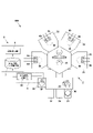
- FIG. 1 is an overall schematic diagram of a semiconductor manufacturing system according to an embodiment of the present invention.
- FIG. It is a figure which shows typically the structure of the radiation temperature measuring apparatus of the same embodiment. It is a figure which shows typically the structure of the spectral characteristic measurement part of the same embodiment. It is a graph which shows the amount of change of the temperature with the transmittance
- the semiconductor manufacturing system 100 of the present embodiment includes a semiconductor manufacturing apparatus 2 having a processing chamber 22 for processing a semiconductor wafer W such as a silicon substrate, and a semiconductor wafer W, which is an object to be measured and placed in the processing chamber 22. and a radiation temperature measuring device 3 for measuring the temperature.
- a semiconductor manufacturing apparatus 2 having a processing chamber 22 for processing a semiconductor wafer W such as a silicon substrate, and a semiconductor wafer W, which is an object to be measured and placed in the processing chamber 22.
- a radiation temperature measuring device 3 for measuring the temperature.
- the semiconductor manufacturing apparatus 2 includes a wafer cassette 21 that stores semiconductor wafers W before and after processing, one or more processing chambers 22 , and a semiconductor device between the wafer cassette 21 and the processing chambers 22 . and a wafer transfer device 23 for transferring the wafer W.
- processing such as film formation, etching, cleaning, surface modification, heating or cooling is performed.
- the radiation temperature measurement device 3 includes two infrared detection units 4a and 4b that detect infrared wavelength bands different from each other, and spectral characteristics for measuring the transmittance and reflectance of each semiconductor wafer W. Based on the transmittance and reflectance of each semiconductor wafer W measured by the measurement unit 5, the amount of infrared rays detected by the two infrared detection units 4a and 4b, and the spectral characteristic measurement unit 5, and a temperature calculator 6 for calculating the temperature.
- the two infrared detection units 4 a and 4 b are provided in the processing chamber 22 .
- the infrared detectors 4a and 4b detect a semiconductor wafer W placed in the processing chamber 22 through a temperature measurement window 22x formed on the wall of the processing chamber 22 and through which infrared rays are transmitted. It detects infrared rays from
- Each of the infrared detection units 4a and 4b is provided between an infrared detection element 41 for detecting infrared rays, a lens 42 for condensing infrared rays on the infrared detection element 41, and between the infrared detection element 41 and the lens 42. and an infrared filter 43 that transmits infrared light in the detection wavelength band.
- the infrared detection element 41 detects infrared rays emitted from the object to be measured and outputs an intensity signal corresponding to the energy of the detected infrared rays. Specifically, the infrared detection element 41 detects infrared rays in the entire infrared wavelength band, for example, and is of a thermal type such as a thermopile. As the infrared detecting element 41, other types such as quantum type photoelectric elements such as HgCdTe, InGaAs, InAsSb, and PbSe may be used.
- the lens 42 is an IR lens that collects the infrared rays emitted from the semiconductor wafer W onto the infrared detection element 41, and has a substantially circular shape with a diameter of about 10 mm to 22 mm in plan view, for example.
- the shape and size of the lens 42 are not limited to those described above, and may be changed as appropriate.
- the infrared filter 43 provided in one infrared detection unit 4a transmits infrared rays of, for example, 7 ⁇ m or more and 9 ⁇ m or less. It allows infrared rays to pass through.
- the spectral characteristic measuring unit 5 is provided in, for example, a chamber 24 different from the processing chamber 22, and measures the transmittance and reflectance of each semiconductor wafer W before being transferred to the processing chamber 22. is.
- the spectral characteristic measurement unit 5 includes an infrared light source 51 that irradiates a semiconductor wafer W with infrared rays in a predetermined wavelength band, and a reflectance sensor 52 that detects infrared rays reflected by the semiconductor wafer W. and a transmittance sensor 53 for detecting infrared rays transmitted through the semiconductor wafer W.
- an infrared light source 51 that irradiates a semiconductor wafer W with infrared rays in a predetermined wavelength band
- a reflectance sensor 52 that detects infrared rays reflected by the semiconductor wafer W.
- a transmittance sensor 53 for detecting infrared rays transmitted through the semiconductor wafer W.
- each infrared light source 51 irradiates infrared rays in a wavelength band including both detection wavelength bands of the two infrared detection units 4a and 4b.
- One infrared light source 51 irradiates all or part of the detection wavelength band of one infrared detection unit 4a, and the other infrared light source 51 emits the detection wavelength of the other infrared detection unit 4b. It is also possible to irradiate all or part of the band with infrared rays.
- Two reflectance sensors 52 and two transmittance sensors 53 are also provided corresponding to the two infrared detection units 4a and 4b.
- One reflectance sensor 52 and transmittance sensor 53 are for detecting infrared rays from one infrared light source 4a, and the other reflectance sensor 52 and transmittance sensor 53 are for detecting infrared light from the other infrared light source. 4b infrared rays are detected.
- a filter 54 is provided in front of the reflectance sensor 52 and the transmittance sensor 53 to transmit the infrared rays in the detection wavelength band of the infrared detectors 4a and 4b.
- the spectral characteristic calculation unit 55 of the spectral characteristic measurement unit 5 calculates the reflectance of the semiconductor wafer W based on the detection signal of the reflectance sensor 52, and calculates the semiconductor wafer W based on the detection signal of the transmittance sensor 53. A transmittance of the wafer W is calculated.
- the spectral characteristic data indicating the reflectance and transmittance of each semiconductor wafer W calculated by the spectral characteristic calculation unit 55 is stored in the spectral characteristic data storage unit 7 .
- the temperature calculation unit 6 calculates the temperature of each semiconductor wafer W based on the amount of infrared rays detected by each of the two infrared detection units 4a and the transmittance and reflectance of each semiconductor wafer W measured by the spectral characteristic measurement unit 5. is calculated.
- the temperature of the semiconductor wafer W is calculated using the following calculation method.
- E 1 (Tx) Amount of infrared rays from the background: E 1 (Tb)
- E 2 (Tx) Amount of infrared rays from semiconductor wafer W viewed from infrared detecting portion 4b of detection wavelength 2 (infrared rays of 8 ⁇ m or more and 14 ⁇ m or less): E 2 (Tx) Amount of infrared rays from the background: E 2 (Tb)
- R 1 and R 2 are the ratios of the amount of infrared rays from the semiconductor wafer W and the amounts of infrared rays from the background.
- the detection wavelengths 1 and 2 are determined so that R 1 ⁇ R 2 , and the unknowns are Tx and Tb.
- E 1 ⁇ 1 ((W 1 ⁇ R 1 E 1 (Tx))/(1 ⁇ R 1 )) E 2 ⁇ 1 ((W 2 ⁇ R 2 E 2 (Tx))/(1 ⁇ R 2 ))
- the model formula can be established taking into account the infrared rays A3 reflected by the semiconductor wafer W and other shielding objects (for example, the light shielding plate 221 in FIG. 2).
- the temperature calculator 6 can correct the temperature of each semiconductor wafer W using the temperature correction parameter resulting from the chamber 22 in which the semiconductor wafer W is accommodated.
- R 1 and R 2 in the above formula (3) are obtained from the respective reflectance and transmittance of the semiconductor wafer W measured by the spectral characteristic measurement unit 5, and the temperature calculation unit 6 calculates the above formula (3). Based on this, the temperature of each semiconductor wafer W is calculated.
- the wafer transfer device 23 transfers the target semiconductor wafer W from the wafer cassette 21 to the chamber 24 for spectral characteristic measurement.
- a spectral characteristic measurement unit 5 provided in a spectral characteristic measurement chamber 24 measures the reflectance and transmittance of the semiconductor wafer W.
- FIG. Spectral characteristic data indicating the measured reflectance and transmittance is stored in the spectral characteristic data storage unit 7 .
- the spectral characteristics of the semiconductor wafer W are measured one by one before being transferred to the processing chamber 22 .
- the wafer transfer device 23 transfers the semiconductor wafer W whose spectral characteristics have been measured to the processing chamber 22 .
- the two infrared detection units 4 a and 4 b detect infrared rays from the semiconductor wafer W through a temperature measurement window 22 x formed in the processing chamber 22 .
- the temperature calculator 6 calculates the temperature of the semiconductor wafer W based on the amount of infrared rays obtained by the two infrared detectors 4a and 4b and the previously measured transmittance and reflectance of the semiconductor wafer W.
- the semiconductor wafer W is processed while the temperature of the semiconductor wafer W is being measured by the radiation temperature measuring device 3 .
- the transmittance of each of the semiconductor wafers W is Since the temperature of each semiconductor wafer W is calculated using the spectral characteristic data indicating the reflectance and the reflectance, the temperature of the semiconductor wafer W can be measured with high accuracy.
- the transmittance of the semiconductor wafer W is less than a predetermined value, R1 ⁇ R2. It becomes difficult to calculate the temperature (dual method). Therefore, in addition to the configuration of the above embodiment, when the transmittance of the semiconductor wafer W is equal to or higher than a predetermined value, the temperature of the semiconductor wafer W is determined using the amount of infrared rays detected by the two infrared detectors 4a and 4b. (dual method), and if the transmittance of the semiconductor wafer W is less than the predetermined value, the temperature of the semiconductor wafer W is calculated using the amount of infrared rays measured by one of the two infrared detectors 4a and 4b. It may be configured as follows (single method). Here, the transmittance of the semiconductor wafer W is the transmittance obtained by the spectral characteristic measurement unit 5 .
- a temperature control mechanism may be provided to adjust the temperature of the semiconductor wafer W when the spectral characteristic measurement unit 5 measures the reflectance and transmittance of the object to be measured.
- the reflectance and transmittance of the semiconductor wafer W adjusted to a desired temperature can be measured.
- the reflectance and transmittance of the semiconductor wafer W can be measured in a state adjusted to the temperature heated in the processing chamber 22, and the temperature of the semiconductor wafer W placed in the processing chamber 22 can be measured with higher accuracy. can be done.
- the spectral characteristics of each semiconductor wafer W are measured before each semiconductor wafer W is transferred to the processing chamber 22.
- the spectral characteristics of each of a plurality of semiconductor wafers W are measured in advance.
- the spectral characteristic data may be stored in the spectral characteristic data storage unit 7 .
- the temperature correction parameter is matched to the measured spectral characteristic data
- the temperature calculation unit 6 corrects the temperature of the semiconductor wafer W by using the spectral characteristic data to which the temperature correction parameter is matched.
- the temperature calculator 6 may calculate the temperature of the semiconductor wafer W from the measured spectral characteristic data and correct the calculated temperature using the temperature correction parameter. Note that the temperature calculator 6 may be configured so as not to correct the temperature using the correction parameter.
- the object W to be measured in the above embodiment is not limited to a semiconductor wafer such as a silicon substrate as long as it is a material that satisfies R1 ⁇ R2.
- the radiation temperature measuring device 3 of the above embodiment was incorporated in the semiconductor manufacturing apparatus 2, it may be of a single configuration that is not incorporated in the semiconductor manufacturing apparatus 2.
Landscapes
- Physics & Mathematics (AREA)
- General Physics & Mathematics (AREA)
- Spectroscopy & Molecular Physics (AREA)
- Radiation Pyrometers (AREA)
Priority Applications (3)
| Application Number | Priority Date | Filing Date | Title |
|---|---|---|---|
| US18/285,428 US20240110834A1 (en) | 2021-04-09 | 2022-03-08 | Radiation temperature measurement device and radiation temperature measurement method |
| EP22784402.4A EP4303547A4 (en) | 2021-04-09 | 2022-03-08 | Radiation temperature measurement device and radiation temperature measurement method |
| JP2023512873A JPWO2022215417A1 (https=) | 2021-04-09 | 2022-03-08 |
Applications Claiming Priority (2)
| Application Number | Priority Date | Filing Date | Title |
|---|---|---|---|
| JP2021066292 | 2021-04-09 | ||
| JP2021-066292 | 2021-04-09 |
Publications (1)
| Publication Number | Publication Date |
|---|---|
| WO2022215417A1 true WO2022215417A1 (ja) | 2022-10-13 |
Family
ID=83546052
Family Applications (1)
| Application Number | Title | Priority Date | Filing Date |
|---|---|---|---|
| PCT/JP2022/010056 Ceased WO2022215417A1 (ja) | 2021-04-09 | 2022-03-08 | 放射温度測定装置及び放射温度測定方法 |
Country Status (4)
| Country | Link |
|---|---|
| US (1) | US20240110834A1 (https=) |
| EP (1) | EP4303547A4 (https=) |
| JP (1) | JPWO2022215417A1 (https=) |
| WO (1) | WO2022215417A1 (https=) |
Cited By (1)
| Publication number | Priority date | Publication date | Assignee | Title |
|---|---|---|---|---|
| WO2024241674A1 (ja) * | 2023-05-25 | 2024-11-28 | 株式会社堀場製作所 | 放射温度測定装置、放射温度測定方法及び放射温度測定装置用プログラム |
Families Citing this family (1)
| Publication number | Priority date | Publication date | Assignee | Title |
|---|---|---|---|---|
| EP4040122B1 (en) * | 2019-10-25 | 2026-02-18 | HORIBA, Ltd. | Radiation thermometer, temperature measurement method, and temperature measurement program |
Citations (5)
| Publication number | Priority date | Publication date | Assignee | Title |
|---|---|---|---|---|
| US4956538A (en) * | 1988-09-09 | 1990-09-11 | Texas Instruments, Incorporated | Method and apparatus for real-time wafer temperature measurement using infrared pyrometry in advanced lamp-heated rapid thermal processors |
| JP2001056253A (ja) * | 1999-08-20 | 2001-02-27 | Toshiba Corp | 温度測定方法及び温度測定装置 |
| JP2002122480A (ja) * | 2000-10-12 | 2002-04-26 | Toshiba Corp | 温度測定方法および装置、並びにプラズマ処理装置 |
| JP2009500851A (ja) * | 2005-07-05 | 2009-01-08 | マットソン テクノロジー インコーポレイテッド | 半導体ウェハの光学的特性を求めるための方法およびシステム |
| JP2017090351A (ja) | 2015-11-13 | 2017-05-25 | 株式会社堀場製作所 | 放射温度計 |
Family Cites Families (11)
| Publication number | Priority date | Publication date | Assignee | Title |
|---|---|---|---|---|
| JPH01202633A (ja) * | 1988-02-08 | 1989-08-15 | Minolta Camera Co Ltd | 放射温度計 |
| US7398693B2 (en) * | 2006-03-30 | 2008-07-15 | Applied Materials, Inc. | Adaptive control method for rapid thermal processing of a substrate |
| JP4921057B2 (ja) * | 2006-07-14 | 2012-04-18 | 大阪瓦斯株式会社 | 放射温度測定装置 |
| JP2008292324A (ja) * | 2007-05-24 | 2008-12-04 | Toyota Motor Corp | 表面温度測定方法および表面温度測定装置 |
| JP5074972B2 (ja) * | 2008-03-24 | 2012-11-14 | 大阪瓦斯株式会社 | 加熱調理器用の温度検出装置 |
| KR101197790B1 (ko) * | 2010-12-27 | 2012-11-05 | 주식회사 포스코 | 복사온도 측정장치 |
| JPWO2016136844A1 (ja) * | 2015-02-25 | 2017-12-07 | 国立大学法人 東京大学 | 温度測定装置及び温度測定方法 |
| CN106052880B (zh) * | 2016-05-24 | 2018-10-30 | 中国航空工业集团公司北京长城计量测试技术研究所 | 基于等效黑体截面的辐射测温距离确定方法 |
| JP2018132476A (ja) * | 2017-02-17 | 2018-08-23 | タキカワエンジニアリング株式会社 | 放射温度測定ユニット |
| JP2020085697A (ja) * | 2018-11-27 | 2020-06-04 | シャープ株式会社 | 赤外線検出装置、赤外線検出方法、コンピュータに実行させるためのプログラムおよびプログラムを記録したコンピュータ読み取り可能な記録媒体 |
| JP2020085696A (ja) * | 2018-11-27 | 2020-06-04 | シャープ株式会社 | 赤外線検出装置、赤外線検出方法、コンピュータに実行させるためのプログラムおよびプログラムを記録したコンピュータ読み取り可能な記録媒体 |
-
2022
- 2022-03-08 JP JP2023512873A patent/JPWO2022215417A1/ja active Pending
- 2022-03-08 EP EP22784402.4A patent/EP4303547A4/en active Pending
- 2022-03-08 US US18/285,428 patent/US20240110834A1/en active Pending
- 2022-03-08 WO PCT/JP2022/010056 patent/WO2022215417A1/ja not_active Ceased
Patent Citations (5)
| Publication number | Priority date | Publication date | Assignee | Title |
|---|---|---|---|---|
| US4956538A (en) * | 1988-09-09 | 1990-09-11 | Texas Instruments, Incorporated | Method and apparatus for real-time wafer temperature measurement using infrared pyrometry in advanced lamp-heated rapid thermal processors |
| JP2001056253A (ja) * | 1999-08-20 | 2001-02-27 | Toshiba Corp | 温度測定方法及び温度測定装置 |
| JP2002122480A (ja) * | 2000-10-12 | 2002-04-26 | Toshiba Corp | 温度測定方法および装置、並びにプラズマ処理装置 |
| JP2009500851A (ja) * | 2005-07-05 | 2009-01-08 | マットソン テクノロジー インコーポレイテッド | 半導体ウェハの光学的特性を求めるための方法およびシステム |
| JP2017090351A (ja) | 2015-11-13 | 2017-05-25 | 株式会社堀場製作所 | 放射温度計 |
Non-Patent Citations (1)
| Title |
|---|
| See also references of EP4303547A4 |
Cited By (1)
| Publication number | Priority date | Publication date | Assignee | Title |
|---|---|---|---|---|
| WO2024241674A1 (ja) * | 2023-05-25 | 2024-11-28 | 株式会社堀場製作所 | 放射温度測定装置、放射温度測定方法及び放射温度測定装置用プログラム |
Also Published As
| Publication number | Publication date |
|---|---|
| JPWO2022215417A1 (https=) | 2022-10-13 |
| EP4303547A1 (en) | 2024-01-10 |
| US20240110834A1 (en) | 2024-04-04 |
| EP4303547A4 (en) | 2025-04-09 |
Similar Documents
| Publication | Publication Date | Title |
|---|---|---|
| US6299346B1 (en) | Active pyrometry with emissivity extrapolation and compensation | |
| US4919542A (en) | Emissivity correction apparatus and method | |
| KR101057853B1 (ko) | 열처리 챔버에서 온도 측정 장치를 캘리브레이팅하기 위한 시스템 및 프로세스 | |
| EP0539984B1 (en) | Method and apparatus for precise temperature measurement | |
| US5114242A (en) | Bichannel radiation detection method | |
| JP5436428B2 (ja) | 較正基板および較正方法 | |
| USRE36050E (en) | Method for repeatable temperature measurement using surface reflectivity | |
| US8786841B2 (en) | Thin film temperature measurement using optical absorption edge wavelength | |
| KR101459668B1 (ko) | 적외선 열화상 카메라를 이용하여 측정된 반도체 소자 온도 분포의 보정 방법 및 이에 이용되는 시스템 | |
| CN107110709B (zh) | 校准cvd或pvd反应器的高温计装置的方法 | |
| JP5702101B2 (ja) | 赤外線センサ信号の補正方法及び温度測定方法並びに温度測定装置 | |
| WO2022215417A1 (ja) | 放射温度測定装置及び放射温度測定方法 | |
| CN105092053B (zh) | 用于mocvd外延生长的三波长免修正红外监测方法及装置 | |
| US8506161B2 (en) | Compensation of stray light interference in substrate temperature measurement | |
| US8496375B2 (en) | Pyrometer adapted for detecting UV-radiation and use thereof | |
| JP2026026307A (ja) | 放射温度計、温度測定方法及び温度測定プログラム | |
| US5364187A (en) | System for repeatable temperature measurement using surface reflectivity | |
| JPH04130746A (ja) | ウエハ温度測定用の放射温度計およびウエハ温度測定方法 | |
| JP2010175442A (ja) | サーモパイル型赤外線検出装置 | |
| CN104089704B (zh) | 半导体薄膜反应腔辅助温度校准方法 | |
| TWM633857U (zh) | 非接觸式之晶圓溫度量測系統 | |
| JPH0456145A (ja) | プラズマ中の基板温度の測定装置 | |
| EP4692742A1 (en) | Radiation temperature measurement device, radiation temperature measurement method, and program for radiation temperature measurement device | |
| CN104697636B (zh) | 一种薄膜生长的自校准实时测温装置 | |
| CN104697638B (zh) | 一种mocvd设备实时测温系统自校准方法 |
Legal Events
| Date | Code | Title | Description |
|---|---|---|---|
| 121 | Ep: the epo has been informed by wipo that ep was designated in this application |
Ref document number: 22784402 Country of ref document: EP Kind code of ref document: A1 |
|
| ENP | Entry into the national phase |
Ref document number: 2023512873 Country of ref document: JP Kind code of ref document: A |
|
| WWE | Wipo information: entry into national phase |
Ref document number: 18285428 Country of ref document: US |
|
| WWE | Wipo information: entry into national phase |
Ref document number: 2022784402 Country of ref document: EP |
|
| ENP | Entry into the national phase |
Ref document number: 2022784402 Country of ref document: EP Effective date: 20231006 |
|
| NENP | Non-entry into the national phase |
Ref country code: DE |