WO2022209368A1 - 固体撮像素子及び固体撮像装置 - Google Patents
固体撮像素子及び固体撮像装置 Download PDFInfo
- Publication number
- WO2022209368A1 WO2022209368A1 PCT/JP2022/005841 JP2022005841W WO2022209368A1 WO 2022209368 A1 WO2022209368 A1 WO 2022209368A1 JP 2022005841 W JP2022005841 W JP 2022005841W WO 2022209368 A1 WO2022209368 A1 WO 2022209368A1
- Authority
- WO
- WIPO (PCT)
- Prior art keywords
- column
- power supply
- solid
- state imaging
- imaging device
- Prior art date
- Legal status (The legal status is an assumption and is not a legal conclusion. Google has not performed a legal analysis and makes no representation as to the accuracy of the status listed.)
- Ceased
Links
Images









Classifications
-
- H—ELECTRICITY
- H04—ELECTRIC COMMUNICATION TECHNIQUE
- H04N—PICTORIAL COMMUNICATION, e.g. TELEVISION
- H04N25/00—Circuitry of solid-state image sensors [SSIS]; Control thereof
- H04N25/60—Noise processing, e.g. detecting, correcting, reducing or removing noise
-
- H—ELECTRICITY
- H04—ELECTRIC COMMUNICATION TECHNIQUE
- H04N—PICTORIAL COMMUNICATION, e.g. TELEVISION
- H04N25/00—Circuitry of solid-state image sensors [SSIS]; Control thereof
- H04N25/70—SSIS architectures; Circuits associated therewith
- H04N25/709—Circuitry for control of the power supply
-
- H—ELECTRICITY
- H04—ELECTRIC COMMUNICATION TECHNIQUE
- H04N—PICTORIAL COMMUNICATION, e.g. TELEVISION
- H04N25/00—Circuitry of solid-state image sensors [SSIS]; Control thereof
- H04N25/70—SSIS architectures; Circuits associated therewith
- H04N25/76—Addressed sensors, e.g. MOS or CMOS sensors
- H04N25/78—Readout circuits for addressed sensors, e.g. output amplifiers or A/D converters
Definitions
- the present disclosure relates to solid-state imaging devices and solid-state imaging devices.
- a pixel value is acquired by outputting a received signal through a vertical signal line based on a column in each line according to a line control signal, and horizontally transferring the output signal. be.
- the voltage and charge of the pixel circuit are reset simultaneously for each line selection control in order to transfer the light receiving signal. Due to the simultaneous execution of the resetting, an influence such as power fluctuation occurs, which may affect the signal output from the pixel circuit. Vertical streaks may also appear due to quantization errors.
- the reset level is distributed in the column direction, etc. A dither effect may occur by having a
- the feedthrough signal generated in the pixel propagates to the comparator via the vertical signal line, and the feedthrough component at the input end of this comparator is attenuated by the parasitic resistance of the vertical signal line.
- the parasitic resistance of the vertical signal line seems to be larger in the pixel line farther from the comparator and smaller in the pixel line closer to the comparator. Therefore, there arises a problem that the dither effect differs relatively according to the distance from the comparator.
- the dither amount is adjusted for a line closer to the comparator, the expected dither amount cannot be obtained for a line farther from the comparator. will result in excessive dither.
- the area and the number of pixels are increasing, and the difference between far and near ends is increasing. Therefore, the difference in parasitic resistance between the pixel line far from the comparator and the pixel line close to the comparator is inevitably large. Since the AD conversion period is determined so as to include the count variation for each column due to dithering, excessive dithering can be a factor in extending the AD period. As a result, there is a high probability that a demerit in terms of processing speed will occur.
- the present disclosure provides a solid-state imaging device that effectively applies dither.
- a solid-state imaging device includes a pixel array, a horizontal control section, a comparator, and a column power supply control section.
- the pixel array includes an array of pixels that photoelectrically convert received light and output signals.
- a horizontal control section selects a line of the pixel array and controls signal output from the pixels belonging to the line.
- the comparator includes a plurality of column comparison circuits that compare output signals from the pixels for each column of the pixel array.
- a column power supply controller controls a power supply voltage for each of the column comparison circuits.
- the column power control unit may include a circuit capable of generating n types of potentials.
- the column power control unit may include n control lines for transmitting n types of potentials.
- the column power supply control unit may include a selector that connects n control lines to the column comparison circuit in m column cycles.
- the selector may transition the connection status between the n control lines and the m-cycle column comparison circuit for each AD conversion.
- the selector may periodically transition the connection status for each AD conversion.
- the selector may transition the connection status after AD conversion based on a random number.
- the unpowered control unit outputs n kinds of potentials to n control lines at the timing of resetting the column comparison circuit, and outputs one kind of potential at the timing of AD conversion.
- the column power supply control unit controls a switch for short-circuiting or opening a power supply line that applies a power supply voltage to the column comparison circuit with the power supply line of another column comparison circuit, and a switching state of the switch. and a switch control circuit that emits a switch control signal to control the switching.
- the column power supply control unit may vary the power supply voltage of each of the column comparison circuits at the timing of resetting the column comparison circuit and the timing of AD conversion.
- the column power control unit may control whether or not to vary the power supply voltage for each AD conversion of the column comparison circuit.
- the column power control unit may control the switches to vary the combination of the column comparison circuits to be short-circuited for each AD conversion.
- a solid-state imaging device includes an optical system that controls a learning environment in the pixel, a solid-state imaging device according to any one of the above, and a signal output from the solid-state imaging device. and a processing circuit.
- FIG. 1 is a block diagram schematically showing a solid-state imaging device according to one embodiment
- FIG. 2 is a block diagram schematically showing part of the circuit of the solid-state imaging device according to one embodiment
- FIG. 3 is a circuit diagram showing an example of a column power supply controller and a comparator according to one embodiment
- 4 is a circuit diagram showing an example of a selector according to one embodiment
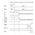
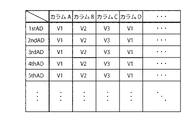
- FIG. 4 is a timing chart in the circuit of the solid-state imaging device according to one embodiment; 4 is a table showing an example of column power control according to one embodiment; 4 is a table showing an example of column power control according to one embodiment;
- FIG. 1 is a circuit diagram showing an example of a control signal delay circuit according to an embodiment;
- FIG. 4 is a table showing an example of column selection to short and open according to one embodiment.
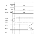
- FIG. 3 is a circuit diagram showing an example of a column power supply controller and a comparator according to one embodiment; 4 is a timing chart in the circuit of the solid-state imaging device according to one embodiment;
- FIG. 3 is a circuit diagram showing an example of a column power supply controller and a comparator according to one embodiment; 4 is a timing chart in the circuit of the solid-state imaging device according to one embodiment;
- 1 is a block diagram showing an example of a schematic configuration of a vehicle control system;
- FIG. FIG. 2 is an explanatory diagram showing an example of installation positions of an information detection unit outside the vehicle and an imaging unit;
- FIG. 1 is a block diagram schematically showing a solid-state imaging device according to one embodiment.
- the solid-state imaging device 1 includes an optical system 10, a power supply section 12, an operation section 14, a control section 16, a display section 18, a solid-state imaging device 20, a storage section 22, and a processing section .
- the solid-state imaging device 1 is a device that converts information acquired from the outside via an optical system 10 into a signal, processes it appropriately, stores it, and outputs it.
- each configuration may be connected via a bus 100 provided in the solid-state imaging device 1 as necessary, or may be directly connected to another appropriate configuration.
- the solid-state imaging device 1 is, for example, a camera installed in a digital camera such as a digital still camera, a smartphone having a shooting function, a tablet terminal, a personal computer, or the like, or installed in various housings such as automobiles and robots. good too.
- the optical system 10 is an optical system such as a lens.
- the optical system 10 is designed and arranged so that the solid-state imaging device 20 can appropriately convert light into signals.
- the optical system 10 may be an independent optical system, or at least part of it may be a microlens or the like formed integrally with the solid-state imaging device 20 on the light receiving portion of the solid-state imaging device 20 .
- the power supply unit 12 has a power supply that appropriately supplies power required for operation in each unit of the solid-state imaging device 1 .
- the operation unit 14 receives user's operations, outputs operation signals according to the user's operations, and notifies each unit regarding the bus 100 .
- the control unit 16 is a circuit that executes control of each unit, and appropriately outputs control signals necessary for controlling each unit.
- the display unit 18 includes, for example, a display of any format for displaying image information obtained by the solid-state imaging device 20 and appropriately signal-processed. In some cases, an image used for operating the operation unit 14 may be displayed. Also, the operation unit 14 and the display unit 18 may be arranged integrally as, for example, a touch panel or a touch display.
- the power supply unit 12, the operation unit 14, and the display unit 18 are not essential components of the solid-state imaging device 1, but appropriately supply power, operation signals, and display via an input/output interface (not shown) provided in the solid-state imaging device 1. Data or the like may be input/output.
- the solid-state imaging device 20 receives light that is appropriately focused via the optical system 10, performs photoelectric conversion, and acquires an analog signal based on the intensity of the received light.
- the solid-state imaging device 20 includes, for example, a photodiode and an organic photoelectric conversion film.
- the solid-state imaging device 20 may further include a DAC (Digital to Analog Converter) to convert this analog signal into a digital signal, perform appropriate signal processing, and then output.
- DAC Digital to Analog Converter
- the storage unit 22 includes a frame memory that temporarily stores the signal output by the solid-state imaging device 20. Furthermore, the storage unit 22 may include storage for storing data necessary for control in the solid-state imaging device 1. FIG.
- the processing unit 24 appropriately processes the signal output by the solid-state imaging device 20 and outputs the processed signal. For example, the processing unit 24 performs processing based on data to be acquired or image processing on the image signal output from the solid-state imaging device 20, and outputs the processed image signal to the storage unit 22 and the display unit .
- the power supply unit 12 has a power supply that appropriately supplies power required for operation in each unit of the solid-state imaging device 1 .
- the operation unit 14 receives user's operations, outputs operation signals according to the user's operations, and notifies each unit regarding the bus 100 .
- the control unit 16 is a circuit that executes control of each unit, and appropriately outputs control signals necessary for controlling each unit.
- the display unit 18 includes, for example, a display of any format for displaying image information obtained by the solid-state imaging device 20 and appropriately signal-processed. In some cases, an image used for operating the operation unit 14 may be displayed. Also, the operation unit 14 and the display unit 18 may be arranged integrally as, for example, a touch panel or a touch display.
- the power supply unit 12, the operation unit 14, and the display unit 18 are not essential components of the solid-state imaging device 1, but appropriately supply power, operation signals, and display via an input/output interface (not shown) provided in the solid-state imaging device 1. Data or the like may be input/output.
- the solid-state imaging device 20 receives light that is appropriately focused via the optical system 10, performs photoelectric conversion, and acquires an analog signal based on the intensity of the received light.
- the solid-state imaging device 20 includes, for example, a photodiode and an organic photoelectric conversion film.
- the solid-state imaging device 20 may further include a DAC (Digital to Analog Converter) to convert this analog signal into a digital signal, perform appropriate signal processing, and then output.
- DAC Digital to Analog Converter
- the storage unit 22 includes a frame memory that temporarily stores the signal output by the solid-state imaging device 20. Furthermore, the storage unit 22 may include storage for storing data necessary for control in the solid-state imaging device 1. FIG.
- the processing unit 24 appropriately processes the signal output by the solid-state imaging device 20 and outputs the processed signal. For example, the processing unit 24 performs processing based on data to be acquired or image processing on the image signal output from the solid-state imaging device 20, and outputs the processed image signal to the storage unit 22 and the display unit .
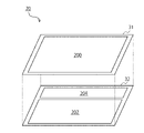
- FIG. 2 is a mounting example of the solid-state imaging device 20.
- the solid-state imaging device 20 includes a light receiving element 200, a storage circuit 202 that is at least part of the storage section 22, and a processing circuit 204 that is at least part of the processing section 24 on the same semiconductor substrate 30.
- FIG. In this manner, one semiconductor substrate 30 may be provided with the light receiving element 200, the storage circuit 202, and the processing circuit 204.
- FIG. Each part is connected by a suitable lead wire or the like.
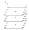
- FIG. 3 is another implementation example of the above.
- the solid-state imaging device 20 may be mounted on the first semiconductor layer 31 and the second semiconductor layer 32, which are different semiconductor layers.
- a light receiving element 200 is provided in the first semiconductor layer 31, and a memory circuit 202 and a processing circuit 204 are provided in the second semiconductor layer 32.
- FIG. The first semiconductor layer 31 and the second semiconductor layer 32 are laminated to form and operate as an integrated semiconductor device.
- the first semiconductor layer 31 is arranged closer to the optical system 10 than the second semiconductor layer 32, the light passing through the optical system 10 is received by the first semiconductor layer 31, and the signal is output to the second semiconductor layer 32. be.
- the solid-state imaging device 20 may be mounted on a first semiconductor layer 31, a second semiconductor layer 32, and a third semiconductor layer 33, which are different semiconductor layers.
- the first semiconductor layer 31 is provided with a light receiving element 200
- the second semiconductor layer 32 is provided with a memory circuit 202
- the third semiconductor layer 33 is provided with a processing circuit 204 .
- the first semiconductor layer 31, the second semiconductor layer 32, and the third semiconductor layer 33 are laminated to form and operate as an integrated semiconductor device.
- the first semiconductor layer 31 is arranged closest to the optical system 10, receives light through the optical system 10 in the first semiconductor layer 31, and outputs a signal to at least one of the second semiconductor layer 32 and the third semiconductor layer 33. is output.
- the stacked semiconductor layers may be formed by, for example, a CoC (Chip on Chip) method in which the semiconductor layers are cut out from the wafer, separated into individual pieces, and then laminated one above the other. good.
- a CoC (Chip on Chip) method may be employed in which any one layer is cut out and individualized and then bonded to a wafer.
- a WoW (Wafer-on-Wafer) method may be adopted, in which each wear is bonded together and then individualized.
- Non-limiting examples of bonding between semiconductor layers include via holes, microbumps, micropads, and plasma bonding.
- the respective semiconductor layers are appropriately electrically connected and formed to be able to transmit and receive signals.
- the solid-state imaging device 20 mounted as described above generates image data by photoelectric conversion in synchronization with the vertical synchronization signal Vsync.
- the vertical synchronizing signal Vsync is a periodic signal with a predetermined frequency that indicates imaging timing.
- the solid-state imaging device 20 appropriately outputs the image data generated based on the timing indicated by the vertical synchronization signal Vsync via the bus 100.
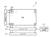
- FIG. 5 is a diagram schematically showing an example of signal output for each column, as an example of signal output from pixels provided as light receiving elements 200 in the solid-state imaging device 20.
- FIG. 5 An example of AD conversion for each column is shown.
- the light receiving element 200 has a pixel array in which pixels 206 are arrayed in the column direction and the line direction.
- a horizontal control unit 208 is a circuit that selects a line of pixels in the pixel array.
- a line of pixels 206 in the light receiving element 200 is selected based on the control signal from the horizontal control unit 208, and pixel signals (analog signals) are output from the pixels belonging to the selected line.
- the comparator 210 compares the analog signal output from the pixel for each column with, for example, a ramp signal obtained by converting a digital signal into an analog signal by DA conversion, amplifies the comparison result, and outputs it for each column. .
- the counter 212 Based on the output from the comparator 210, the counter 212 outputs the pixel value output from each pixel 206 as a digital signal.
- the solid-state imaging device 20 in this embodiment further includes a column power supply control section 214.
- the column power supply control unit 214 is a circuit that controls the power supply voltage of the comparison circuit provided for each column in the comparator 210 . By locally controlling the power supply voltage for each column by the column power supply control unit 214, the solid-state imaging device 20 of the present embodiment realizes appropriate dither processing.
- FIG. 6 is a diagram showing an example of the comparator 210 in the solid-state imaging device 20 according to this embodiment and the column power supply control section 214 that controls the local power supply for each column.
- the comparator 210 in the solid-state imaging device 20 according to this embodiment and the column power supply control section 214 that controls the local power supply for each column.
- three different local power supply voltages are used to perform dither processing.
- the three voltages are shown as a non-limiting example, and the voltage of the local power supply may be two, or four or more.
- the comparator 210 includes column comparison circuits 210A, 210B, 210C, . . . for each column.
- the subscripts A, B, and C are letters that identify columns.
- Each column comparison circuit is desirably composed of the same circuit.
- the configuration will be described using the column comparison circuit 210A as an example.
- the column comparison circuit 210A includes capacitors C1, C2, C3, transistors M1, M2, M3, M4, switches SW1, SW2, and an NOT circuit N1.
- Capacitors C1 and C2 constitute an auto-zero capacitance. One end of the capacitor C1 is connected to the vertical signal line VSL for each column. A ramp signal Ramp is input to one end of the capacitor C2. The other ends of the capacitors C1 and C2 are connected, and the signal from the pixel is superimposed on the ramp signal Ramp to output the signal DIFFDAC.
- the transistor M1 is, for example, a p-type MOSFET (Metal-Oxide-Semiconductor Field-Effect Transistor), has a source connected to the column power supply control unit 214 to which the power supply voltage VDDA is applied, and a gate connected to the capacitors C1 and C2. DIFFDAC is applied at
- the transistor M2 is, for example, an n-type MOSFET, and has a drain connected to the drain of the transistor M1 and a source connected to the power supply voltage VSS. This transistor M2 operates as a first current source. An appropriate bias voltage is applied to the gate of the transistor M2 to allow a drain current based on the potential of the drain to flow.
- a signal VOUT1 is output to the gate of the transistor M3 between the drains of the transistors M1 and M2.
- the switch SW1 is connected between the gate and drain of the transistor M1.
- the switch SW1 controls short-circuiting and opening between the gate and drain of the transistor M1 by the auto-zero signal AZP.
- the gate of the transistor M1 is connected to the power supply voltage VSS through the transistor M2, resetting the charges of the capacitors C1 and C2.
- the transistor M3 is, for example, a p-type MOSFET, has a source connected to the column power supply control unit 214 to which the power supply voltage VDDA is applied, and a gate connected to the drain of the transistor M1.
- the transistor M4 is, for example, an n-type MOSFET, and has a drain connected to the drain of the transistor M3, a gate connected to one end of the capacitor C3, and a source connected to the power supply voltage VSS. This transistor M4 operates as a second current source.
- a signal VOUT2 is output to the NOT circuit N1 between the drains of the transistors M3 and M4.
- Capacitor C3 is a capacitor that generates the potential of the gate of transistor M4 that operates as a second current source.
- the switch SW2 is connected between the gate and drain of the transistor M4.
- the switch SW1 controls short-circuiting and opening between the gate and drain of the transistor M4 by the auto-zero signal AZN.
- the gate of the transistor M4 is connected to the drain to reset the potential of the gate.
- the NOT circuit N1 is a circuit that inverts the input and outputs it, inverts the input VOUT2, and outputs the output signal OUT from the comparator.
- clamp circuits may be connected before and after the NOT circuit N1. This clamp circuit may be a circuit that can be selectively output from the comparator.
- This circuit is an example circuit, and the circuit of the comparator for the column is not limited to the example in FIG.
- the column power supply control unit 214 includes a selector 216 and local power supplies 218A, 218B, 218C, .
- the column power supply control unit 214 is a circuit that applies an appropriate power supply voltage to the column comparison circuits 210A, 210B, 210C, .
- the selector 216 is a circuit that receives the control signal Cnt and the voltages V1, V2, and V3 that serve as local power supplies and outputs appropriate voltages to appropriate output destinations. The selector 216 selects which voltage to output to which column according to the control signal Cnt.
- the local power supply 218A is a circuit that controls and outputs the power supply voltage for the column comparison circuit 210A.
- the local power supply 218A is connected to the power supply voltage VDD, controls the voltage output from the selector 216 to a stable voltage, and outputs the power supply voltage VDDA to the power supply terminal of the column comparison circuit 210A.
- Each of the local power supplies 218 may be configured with a regulator such as an LDO (Low Dropout), for example.
- the local power supply 218 preferably uses a regulator that outputs a stable voltage for a plurality of voltage values, for example, a regulator that can supply an appropriately stable voltage even if the input/output voltage has a certain width.
- the selector 216 connects the power supply voltage V1 to the local power supply 218A.
- the local power supply 218A converts the input voltage into a stable voltage V1 and outputs it to the column comparison circuit 210A as a power supply voltage.
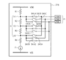
- FIG. 7 is a circuit diagram showing a non-limiting example of the selector 216.
- FIG. Selector 216 includes resistors R1, R2, R3, R4, current source I1, and switches SW1A, SW1B, SW1C, SW2A, SW2B, SW2C, SW3A, SW3B, SW3C.
- the resistors R1, R2, R3, R4 and the current source I1 are connected in series between the power supply voltages VDD and VSS. These resistors and current sources produce different voltages at the junctions of the resistors. For example, assume that the node potential of the resistors R1 and R2 is V1, the node potential of the resistors R2 and R3 is V2, and the node potential of the resistors R3 and R4 is V3.
- switches SW1A, SW2A, and SW3A are exclusively controlled by the control signal Cnt.
- switches SW1B, SW2B, SW3B and switches SW1C, SW2C, SW3C are controlled exclusively.
- switches SW1A, SW2B, and SW3C are turned on, and the other switches are turned off.
- voltage V1 is output to local power supply 218A
- voltage V2 is output to local power supply 218B
- voltage V3 is output to local power supply 218C.
- FIG. 8 is a timing chart when the selector 216 is connected as shown in FIG.
- the solid line represents the input and output of the column with supply voltages V1 and V1 selected
- the dotted line represents the input and output of the column with V2 and V2 selected
- the dashed line represents V3.
- V3 represent the input/output of the selected column.
- the column comparison circuits 210A, 210B, 210C, . . . are reset.
- column power supply control section 214 controls voltages V1, V2, and V3.
- each capacitor in the column comparison circuit 210A etc. is appropriately set to the reset level based on the power supply voltages V1, V2 and V3 applied to each column.
- V1 and V3 may be equal to V2. It should be noted that it is not necessary to set the voltage to V2, and it is sufficient to control the potential to be the same at the timing of AD execution.
- VOUT1 is output at the timing based on the pixel value and the reset level of the capacitor.
- a signal based on the transition timing of VOUT1 is output from each of the column comparison circuits 210A and the like by changing the gate potential of the transistor M3 due to this VOUT1.
- the difference in the voltages of V1, V2, and V3 can shift the timing of outputting OUT, and dither processing can be performed appropriately.
- FIG. 9 is a table showing a non-limiting example of control by the column power supply control unit 214.
- FIG. As shown in this figure, three power supply voltages may be applied in sequence to the three columns. As shown in this example, the power supply voltage applied to the columns may be controlled periodically. By changing the power supply voltage in this way, dither processing can be performed in the column direction at the same timing, and dither processing in the time direction can be performed in the same column for each AD.
- Random numbers are not limited to uniform random numbers, and may be random numbers based on, for example, normal distribution, Poisson distribution, binomial distribution, or the like. When random numbers are used, different random numbers may be used for each column, or column A and column D may have periodicity in the column direction such that the same power supply voltage is used as described above. That is, although the voltage applied to column A is randomly determined, column A and column D may always be applied with the same power supply voltage.
- the selector 216 may change the input/output relationship for each AD.
- the output timing of the P phase in the same column can be changed in the time direction.
- FIG. 10 is a table showing another non-limiting example of control by the column power supply control unit 214.
- FIG. 10 As shown in this figure, three power supply voltages may be applied to three columns regardless of time. In this case, as shown in FIG. 9, dither processing in the time direction cannot be implemented, but dither processing in the column direction can be appropriately performed.
- adjacent columns may be controlled so that different power supply voltages are applied.
- the voltage to be applied in the column direction may be determined by random numbers so that the same power supply voltage is not applied continuously to a predetermined value (for example, three or more columns) without being limited to the columns to be matched.
- the types of signals selected by the selector 216 and the period of the columns for distributing the signals are not limited to three.
- the selector 216 is provided with input lines to which n types of potentials are input as power supply voltage inputs, or is provided with a power supply for which n types of potentials can be set in the selector 216 .
- the selector 216 has a circuit configuration that can selectively output n types of power supply voltages appropriately to m types of columns.
- the column power control unit 214 includes a circuit capable of generating n kinds of potentials and a selection circuit capable of controlling the connection relationship of the n control lines.
- the n control lines are connected to the local power supply means corresponding to each column, for example, in m column cycles.
- FIG. 11 is a circuit diagram showing an example of the column power supply controller 214 according to the second embodiment.
- a switch is further arranged for short-circuiting the power supply voltage terminals of adjacent columns.
- a switch SWab is arranged between the lines for applying the power supply voltage between columns A and B, and a switch SWbc is arranged between columns B and C. These switches are controlled by a control signal Cntsw.
- the column power control unit 214 may further include a switch control circuit (not shown) that outputs this control signal Cntsw.
- FIG. 12 is a timing chart when the selector 216 is connected as shown in FIG. As shown in FIG. 12, the control signal Cntsw is switched from on to off before AZP and AZN are switched from on to off. This timing is set so that the auto-zero is turned off before VDDA rises and falls. That is, the capacitors are reset for each column at the power supply voltage indicated by the dashed line in the figure.
- the present embodiment as well, it is possible to perform control to vary the power supply voltage applied to each column. By superimposing this variation on the reset level of the AD conversion, it is possible to give variation to the count in the P phase.
- the dither amount can be controlled by the timing of AZ and Cntsw.
- the short-circuited columns vary by the Vth mismatch starting from the averaged potential. As a result, the average value of the power supply voltage itself does not fluctuate.
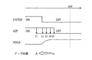
- FIG. 13 is a diagram showing the relationship between AZP according to the present embodiment and the magnitude of the dither effect due to the timing of Cntsw.
- Cntsw is turned off before AZ above, it is not limited to this. For example, you can turn off AZP first, then turn on Cntsw. Also, Cntsw may be turned on at the same time as AZP. For example, when V1 is higher than the average power supply voltage in the short-circuited column, the power supply potential of column A connected to V1 transitions as shown by V1 in FIG. Assume that AD conversion is started from tad in this state.
- the dither amount increases because the difference between VDDA at reset and AD conversion is greater than at t2 to t5.
- the difference between VDDA at the time of resetting and at the time of AD conversion is smaller compared to t1 to t3, so the amount of dither increases. In this way, it is also possible to control the dither amount by the switching timing of AZP or the switching timing of Cntsw.
- dithering/non-execution may be switched for each AD conversion. For example, by controlling Cntsw while it is off, dither processing is not performed in adjacent columns. By switching this for each AD conversion, dither processing can be performed in the time direction.
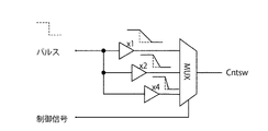
- Fig. 14 is a circuit that generates Cntsw with different fall timings from ON to OFF.
- the control signal is a selection signal that controls which of the multiple input signals is selected for the multiplexer MUX.
- the multiplexer MUX receives signals with different fall timings that have passed through different numbers of buffers. By outputting a desired signal from the multiplexer MUX according to the control signal among the signals with different falling timings, the desired signal can be output when the dither amount is controlled by the timing as shown in FIG. Of course, this circuit may also be provided in the column power supply controller 214 .
- the dotted line indicates the timing of the input pulse, and each buffer outputs the falling pulse indicated by the solid line with different timing.
- the control signal may be set so as to set an appropriate reset level for each column periodically, as in the above-described embodiment, or the setting may be updated by random numbers or the like for each AD. good too.
- Fig. 15 is a circuit that virtually generates Cntsw with different fall timings from on to off.
- the control signal is the same as in FIG. 14 and may be periodic or random.
- the circuit in FIG. 15 differs in the drive capability of the buffer input to the multiplexer MUX. Due to this difference in drive capability, for example, the output of each buffer outputs a sharper signal as the drive capability is higher and a duller signal as the drive capability is lower, as shown in the upper right of the buffer. This signal is appropriately output from the multiplexer MUX by a control signal.
- the amount of dither can be controlled by shifting the timing when the switch SWab falls below the threshold voltage at which the switch SWab turns off.
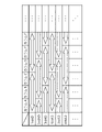
- Fig. 16 is a table showing another example of short-circuit and open-circuit control for dithering in the time direction.
- Columns to which the same arrow belongs are columns to be short-circuited or opened in each AD conversion. In this way, the columns to be short-circuited and open-circuited may be changed for each AD conversion process.
- the column connection relationship is controlled periodically, but the column connection relationship may be controlled randomly instead of periodically. For example, like a random walk, the connection relationship may be shifted to the left or right (the position of the arrow in FIG. 14 may be moved left or right or not moved).
- a comparison circuit that does not perform differential operation is selected as the comparison circuit for each column, but the present invention is not limited to this.
- the technique of the present disclosure can be applied even to a circuit that compares a ramp signal and a signal from a pixel based on a differential signal.
- FIG. 17 is a circuit diagram showing the column comparison circuit 210A in this embodiment.
- the column comparison circuit 210A receives the ramp signal Ramp and the signal from the vertical signal line VSL from the pixels as differential inputs, and acquires the timing signal in the counter circuit based on the difference between these signals.
- This circuit is given as a non-limiting example of a comparator using a differential amplifier, and can be applied to other circuits as well.
- the switches SWr and SWv are, for example, connected between the gate and drain of n-type MOSFETs, which are the input terminals of the respective signals installed in the lower stage, as shown in the figure.
- the autozero signals AZR, AZV properly reset the respective input transistors.
- AZR and AZV are switched on/off at the same time. dither effect can be obtained.
- FIG. 18 is a diagram showing an example of a timing chart in this embodiment. As shown in FIG. 18, first, before controlling V1 and the like, AZV is turned off to release the reset state of the transistor to which the signal from the pixel is input.
- the dither effect can be exhibited by varying the reset level for receiving the signal from the pixel and the reset level for receiving the ramp signal.
- FIG. 19 shows the comparison circuit of the second embodiment as a differential input type.
- the configuration is the same as that of FIG. 17 except that there is a switch for short-circuiting and opening between columns. That is, it is presented as a non-limiting example of a comparator that accepts differential inputs.
- FIG. 20 is a diagram showing a timing chart in the case of FIG. Similarly in this case, after turning off Cntsw, first, AZV is turned off to set the reset level of the transistor on the pixel side. After this, the reset level of the input transistor on the ramp signal side is set.
- the technology (this technology) according to the present disclosure can be applied to various products.
- the technology according to the present disclosure can be realized as a device mounted on any type of moving body such as automobiles, electric vehicles, hybrid electric vehicles, motorcycles, bicycles, personal mobility, airplanes, drones, ships, and robots. may
- FIG. 21 is a block diagram showing a schematic configuration example of a vehicle control system, which is an example of a mobile control system to which the technology according to the present disclosure can be applied.
- a vehicle control system 12000 includes a plurality of electronic control units connected via a communication network 12001.
- the vehicle control system 12000 includes a driving system control unit 12010, a body system control unit 12020, a vehicle exterior information detection unit 12030, a vehicle interior information detection unit 12040, and an integrated control unit 12050.
- a microcomputer 12051, an audio/image output unit 12052, and an in-vehicle network I/F (Interface) 12053 are illustrated.
- the drive system control unit 12010 controls the operation of devices related to the drive system of the vehicle according to various programs.
- the driving system control unit 12010 includes a driving force generator for generating driving force of the vehicle such as an internal combustion engine or a driving motor, a driving force transmission mechanism for transmitting the driving force to the wheels, and a steering angle of the vehicle. It functions as a control device such as a steering mechanism to adjust and a brake device to generate braking force of the vehicle.
- the body system control unit 12020 controls the operation of various devices equipped on the vehicle body according to various programs.
- the body system control unit 12020 functions as a keyless entry system, a smart key system, a power window device, or a control device for various lamps such as headlamps, back lamps, brake lamps, winkers or fog lamps.
- the body system control unit 12020 can receive radio waves transmitted from a portable device that substitutes for a key or signals from various switches.
- the body system control unit 12020 receives the input of these radio waves or signals and controls the door lock device, power window device, lamps, etc. of the vehicle.
- the vehicle exterior information detection unit 12030 detects information outside the vehicle in which the vehicle control system 12000 is installed.
- the vehicle exterior information detection unit 12030 is connected with an imaging section 12031 .
- the vehicle exterior information detection unit 12030 causes the imaging unit 12031 to capture an image of the exterior of the vehicle, and receives the captured image.
- the vehicle exterior information detection unit 12030 may perform object detection processing or distance detection processing such as people, vehicles, obstacles, signs, or characters on the road surface based on the received image.
- the imaging unit 12031 is an optical sensor that receives light and outputs an electrical signal according to the amount of received light.
- the imaging unit 12031 can output the electric signal as an image, and can also output it as distance measurement information.
- the light received by the imaging unit 12031 may be visible light or non-visible light such as infrared rays.
- the in-vehicle information detection unit 12040 detects in-vehicle information.
- the in-vehicle information detection unit 12040 is connected to, for example, a driver state detection section 12041 that detects the state of the driver.
- the driver state detection unit 12041 includes, for example, a camera that captures an image of the driver, and the in-vehicle information detection unit 12040 detects the degree of fatigue or concentration of the driver based on the detection information input from the driver state detection unit 12041. It may be calculated, or it may be determined whether the driver is dozing off.
- the microcomputer 12051 calculates control target values for the driving force generator, the steering mechanism, or the braking device based on the information inside and outside the vehicle acquired by the vehicle exterior information detection unit 12030 or the vehicle interior information detection unit 12040, and controls the drive system control unit.
- a control command can be output to 12010 .
- the microcomputer 12051 realizes the functions of ADAS (Advanced Driver Assistance System) including collision avoidance or shock mitigation of vehicles, follow-up driving based on inter-vehicle distance, vehicle speed maintenance driving, vehicle collision warning, vehicle lane deviation warning, etc. Cooperative control can be performed for the purpose of ADAS (Advanced Driver Assistance System) including collision avoidance or shock mitigation of vehicles, follow-up driving based on inter-vehicle distance, vehicle speed maintenance driving, vehicle collision warning, vehicle lane deviation warning, etc. Cooperative control can be performed for the purpose of ADAS (Advanced Driver Assistance System) including collision avoidance or shock mitigation of vehicles, follow-up driving based on inter-vehicle distance, vehicle speed maintenance driving
- the microcomputer 12051 controls the driving force generator, the steering mechanism, the braking device, etc. based on the information about the vehicle surroundings acquired by the vehicle exterior information detection unit 12030 or the vehicle interior information detection unit 12040, so that the driver's Cooperative control can be performed for the purpose of autonomous driving, etc., in which vehicles autonomously travel without depending on operation.
- the microcomputer 12051 can output a control command to the body system control unit 12030 based on the information outside the vehicle acquired by the information detection unit 12030 outside the vehicle.
- the microcomputer 12051 controls the headlamps according to the position of the preceding vehicle or the oncoming vehicle detected by the vehicle exterior information detection unit 12030, and performs cooperative control aimed at anti-glare such as switching from high beam to low beam. It can be carried out.
- the audio/image output unit 12052 transmits at least one of audio and/or image output signals to an output device capable of visually or audibly notifying the passengers of the vehicle or the outside of the vehicle.
- an audio speaker 12061, a display unit 12062 and an instrument panel 12063 are illustrated as output devices.
- the display unit 12062 may include at least one of an on-board display and a head-up display, for example.
- FIG. 22 is a diagram showing an example of the installation position of the imaging unit 12031.
- the imaging unit 12031 has imaging units 12101, 12102, 12103, 12104, and 12105.
- the imaging units 12101, 12102, 12103, 12104, and 12105 are provided at positions such as the front nose, side mirrors, rear bumper, back door, and windshield of the vehicle 12100, for example.
- An image pickup unit 12101 provided in the front nose and an image pickup unit 12105 provided above the windshield in the passenger compartment mainly acquire images in front of the vehicle 12100 .
- Imaging units 12102 and 12103 provided in the side mirrors mainly acquire side images of the vehicle 12100 .
- An imaging unit 12104 provided in the rear bumper or back door mainly acquires an image behind the vehicle 12100 .
- the imaging unit 12105 provided above the windshield in the passenger compartment is mainly used for detecting preceding vehicles, pedestrians, obstacles, traffic lights, traffic signs, lanes, and the like.
- FIG. 22 shows an example of the imaging range of the imaging units 12101 to 12104.
- the imaging range 12111 indicates the imaging range of the imaging unit 12101 provided in the front nose
- the imaging ranges 12112 and 12113 indicate the imaging ranges of the imaging units 12102 and 12103 provided in the side mirrors, respectively
- the imaging range 12114 The imaging range of an imaging unit 12104 provided on the rear bumper or back door is shown. For example, by superimposing the image data captured by the imaging units 12101 to 12104, a bird's-eye view image of the vehicle 12100 viewed from above can be obtained.
- At least one of the imaging units 12101 to 12104 may have a function of acquiring distance information.
- at least one of the imaging units 12101 to 12104 may be a stereo camera composed of a plurality of imaging elements, or may be an imaging element having pixels for phase difference detection.
- the microcomputer 12051 determines the distance to each three-dimensional object within the imaging ranges 12111 to 12114 and changes in this distance over time (relative velocity with respect to the vehicle 12100). , it is possible to extract, as the preceding vehicle, the closest three-dimensional object on the traveling path of the vehicle 12100, which runs at a predetermined speed (for example, 0 km/h or more) in substantially the same direction as the vehicle 12100. can. Furthermore, the microcomputer 12051 can set the inter-vehicle distance to be secured in advance in front of the preceding vehicle, and perform automatic brake control (including following stop control) and automatic acceleration control (including following start control). In this way, cooperative control can be performed for the purpose of automatic driving in which the vehicle runs autonomously without relying on the operation of the driver.
- automatic brake control including following stop control
- automatic acceleration control including following start control
- the microcomputer 12051 converts three-dimensional object data related to three-dimensional objects to other three-dimensional objects such as motorcycles, ordinary vehicles, large vehicles, pedestrians, and utility poles. It can be classified and extracted and used for automatic avoidance of obstacles. For example, the microcomputer 12051 distinguishes obstacles around the vehicle 12100 into those that are visible to the driver of the vehicle 12100 and those that are difficult to see. Then, the microcomputer 12051 judges the collision risk indicating the degree of danger of collision with each obstacle, and when the collision risk is equal to or higher than the set value and there is a possibility of collision, an audio speaker 12061 and a display unit 12062 are displayed. By outputting an alarm to the driver via the drive system control unit 12010 and performing forced deceleration and avoidance steering via the drive system control unit 12010, driving support for collision avoidance can be performed.
- At least one of the imaging units 12101 to 12104 may be an infrared camera that detects infrared rays.
- the microcomputer 12051 can recognize a pedestrian by determining whether or not the pedestrian exists in the captured images of the imaging units 12101 to 12104 .
- recognition of a pedestrian is performed by, for example, a procedure for extracting feature points in images captured by the imaging units 12101 to 12104 as infrared cameras, and performing pattern matching processing on a series of feature points indicating the outline of an object to determine whether or not the pedestrian is a pedestrian.
- the audio image output unit 12052 outputs a rectangular outline for emphasis to the recognized pedestrian. is superimposed on the display unit 12062 . Also, the audio/image output unit 12052 may control the display unit 12062 to display an icon or the like indicating a pedestrian at a desired position.
- the technology according to the present disclosure can be applied to the imaging unit 12031 among the configurations described above.
- the solid-state imaging device in FIG. 1 and the like and the solid-state imaging element in FIG. 5 and the like can be applied to the imaging unit 12031.
- a pixel array having an array of pixels that photoelectrically convert received light and output signals; a horizontal control unit that selects a line of the pixel array and controls signal output from the pixels belonging to the line; a comparator comprising a plurality of column comparison circuits for comparing output signals from the pixels for each column of the pixel array; a column power supply controller that controls a power supply voltage for each of the column comparison circuits; A solid-state image sensor.
- the column power supply control unit includes a circuit capable of generating n types of potentials, The solid-state imaging device according to (2).
- the column power control unit includes n control lines that transmit n types of potentials, The solid-state imaging device according to (3).
- the solid-state imaging device according to (4).
- the column power supply control unit includes a selector that connects n control lines to the column comparison circuit in m column cycles, The solid-state imaging device according to (5).
- the selector transitions the connection status between the n control lines and the m-cycle column comparison circuit for each AD conversion.
- the selector periodically transitions the connection status for each AD conversion with respect to time;
- the solid-state imaging device according to (7).
- the column power supply control unit controls short-circuiting and opening of a power supply line that applies a power supply voltage to the column comparison circuit with the power supply line of another column comparison circuit; a switch control circuit for transmitting a switch control signal for controlling the switching state of the switch; comprising (1) The solid-state imaging device according to (1).
- the column power supply control unit varies the power supply voltage of each of the column comparison circuits at the timing of resetting the column comparison circuit and the timing of AD conversion.
- the column power supply control unit controls whether or not to vary the power supply voltage for each AD conversion of the column comparison circuit.
- the column power control unit controls the switch for each AD conversion, and varies the combination of the column comparison circuits to be short-circuited.
- (11) The solid-state imaging device according to (11).
- an optical system that controls a learning environment in the pixel; a solid-state imaging device according to any one of (1) to (14); a processing circuit that processes a signal output from the solid-state imaging device; A solid-state imaging device.
Landscapes
- Engineering & Computer Science (AREA)
- Multimedia (AREA)
- Signal Processing (AREA)
- Transforming Light Signals Into Electric Signals (AREA)
Abstract
[課題]ディザを効果的に付与する。 [解決手段]固体撮像素子は、画素アレイと、水平方向制御部と、コンパレータと、カラム電源制御部と、を備える。画素アレイは、受光した光を光電変換して信号を出力する画素をアレイ状に備える。水平方向制御部は、前記画素アレイのラインを選択し、前記ラインに属する前記画素からの信号出力を制御する。コンパレータは、前記画素アレイのカラムごとに前記画素からの出力信号を比較する複数のカラム比較回路を備える。カラム電源制御部は、前記カラム比較回路のそれぞれに対する電源電圧を制御する。
Description
本開示は、固体撮像素子及び固体撮像装置に関する。
撮像装置では、受光した信号を、ライン制御信号にしたがってそれぞれのラインにおけるカラムに基づいて垂直信号線を介して出力し、この出力された信号を水平転送することにより、画素値を取得する手法がある。このような手法においては、ラインの選択制御ごとに、受光信号を転送するために、画素回路の電圧、電荷のリセットが一斉に実行される。一斉にリセットが実行されることにより、電源変動等の影響が発生し、画素回路から出力される信号に影響を及ぼすことがある。また、量子化誤差による縦筋が現れることもある。これらに対して、画素リセット時の信号線へのフィードスルーの振幅やフィードスルーのセトリング時間が画素ごとに異なることを利用し、リセットレベルをカラム方向に分布させる等、セトリングしきらないタイミングでばらつきを持たせることによりディザ効果を発生させることがある。
しかしながら、画素で発生したフィードスルー信号は、垂直信号線を介して比較器に伝搬し、この比較器の入力端でのフィードスルー成分は、垂直信号線の寄生抵抗により減衰する。また、垂直信号線の寄生抵抗は、比較器から遠い画素ラインほど大きく、比較器から近い画素ラインほど小さく見える。したがって、相対的に、比較器からの距離に応じてディザ効果が異なるという問題が発生する。
具体的には、ディザ量を比較器から近いラインに合わせて調整すると、遠いラインにおいては期待したディザ量が得ることができず、一方で、比較器から遠いラインに合わせて調整すると、近いラインにおいては過剰なディザとなる。また近年、高解像度で高感度な静止画又は動画を取得するために、大面積化、多画素化が進んでおり、遠近端差が大きくなっている。そのため、比較器と遠い画素ラインと近い画素ラインとの寄生抵抗の差も必然的に大きくなっている。AD変換を行う期間はディザによるカラム毎のカウントばらつきを包含するように決定されるため、過剰なディザはAD期間を延ばす要因となり得る。結果的に、処理速度的にデメリットが生じる蓋然性が高い。
そこで、本開示では、ディザを効果的に付与する、固体撮像装置を提供する。
一実施形態によれば、固体撮像素子は、画素アレイと、水平方向制御部と、コンパレータと、カラム電源制御部と、を備える。画素アレイは、受光した光を光電変換して信号を出力する画素をアレイ状に備える。水平方向制御部は、前記画素アレイのラインを選択し、前記ラインに属する前記画素からの信号出力を制御する。コンパレータは、前記画素アレイのカラムごとに前記画素からの出力信号を比較する複数のカラム比較回路を備える。カラム電源制御部は、前記カラム比較回路のそれぞれに対する電源電圧を制御する。
前記カラム電源制御部は、n (n >= 2)種類の電源電圧を前記カラム比較回路のそれぞれに印加してもよい。
前記カラム電源制御部は、n種類の電位が生成可能な回路を備えてもよい。
前記カラム電源制御部は、n種類の電位を伝達するn本の制御線を備えてもよい。
前記カラム電源制御部は、m (m >= 2)個の前記カラム比較回路ごとに、同じ電源電圧を印加してもよい。
前記カラム電源制御部は、n本の制御線をmカラム周期で前記カラム比較回路と接続させる、セレクタ、を備えてもよい。
前記セレクタは、AD変換ごとに、n本の制御線とm周期の前記カラム比較回路との接続状況を遷移させてもよい。
前記セレクタは、時間に対する周期的に、AD変換ごとの接続状況を遷移させてもよい。
前記セレクタは、乱数に基づいて、AD変換後との接続状況を遷移させてもよい。
前記から無電源制御部は、n本の制御線に対して、前記カラム比較回路のリセットのタイミングにおいては、n種類の電位を出力し、AD変換のタイミングにおいては、1種類の電位を出力させてもよい。
前記カラム電源制御部は、前記カラム比較回路に電源電圧を印加する電源線について、他の前記カラム比較回路の前記電源線との短絡、開放を制御する、スイッチと、前記スイッチの切替状態を制御するスイッチ制御信号を発信する、スイッチ制御回路と、を備えてもよい。
前記カラム電源制御部は、前記カラム比較回路のリセットのタイミングと、AD変換のタイミングと、において、それぞれの前記カラム比較回路の電源電圧を変動させてもよい。
前記カラム電源制御部は、前記カラム比較回路のAD変換ごとに、電源電圧を変動させるか、させないかを制御してもよい。
前記カラム電源制御部は、AD変換ごとに、前記スイッチを制御し、短絡する前記カラム比較回路の組み合わせを変動させてもよい。
一実施形態によれば、固体撮像装置は、前記画素における受講環境を制御する、光学系と、上記のいずれかに記載の固体撮像素子と、前記固体撮像素子から出力される信号を処理する、処理回路と、を備える。
以下、図面を参照して本開示における実施形態の説明をする。図面は、説明のために用いるものであり、実際の装置における各部の構成の形状、サイズ、又は、他の構成とのサイズの比等が図に示されている通りである必要はない。また、図面は、簡略化して書かれているため、図に書かれている以外にも実装上必要な構成は、適切に備えるものとする。
(第1実施形態)
図1は、一実施形態に係る固体撮像装置を模式的に示すブロック図である。固体撮像装置1は、光学系10と、電源部12と、操作部14と、制御部16と、表示部18と、固体撮像素子20と、記憶部22と、処理部24と、を備える。固体撮像装置1は、外部から光学系10を介して取得した情報を信号に変換し、適切に処理して格納、出力する装置である。各構成は、例えば、必要に応じて固体撮像装置1に備えられるバス100を介して接続されてもよいし、直接的に適切な他の構成と接続されてもよい。
図1は、一実施形態に係る固体撮像装置を模式的に示すブロック図である。固体撮像装置1は、光学系10と、電源部12と、操作部14と、制御部16と、表示部18と、固体撮像素子20と、記憶部22と、処理部24と、を備える。固体撮像装置1は、外部から光学系10を介して取得した情報を信号に変換し、適切に処理して格納、出力する装置である。各構成は、例えば、必要に応じて固体撮像装置1に備えられるバス100を介して接続されてもよいし、直接的に適切な他の構成と接続されてもよい。
固体撮像装置1は、例えば、デジタルスチルカメラ等のデジタルカメラ、撮影機能を備えるスマートフォン、タブレット端末、パーソナルコンピュータ等に搭載され、又は、自動車、ロボット等の各種筐体に備えられるカメラ等であってもよい。
光学系10は、レンズ等の光学系である。光学系10は、固体撮像素子20において適切に光から信号へと変換ができるように設計、配置される。光学系10は、独立した光学系であってもよいし、少なくともその一部が、固体撮像素子20の受光部上に固体撮像素子20と一体として形成されるマイクロレンズ等であってもよい。
電源部12は、固体撮像装置1の各部において動作に必要となる電力を適切に供給する電源を有する。
操作部14は、ユーザの操作を受け付け、ユーザの操作にしたがった操作信号を出力し、バス100を関して各部に通知する。
制御部16は、各部の制御を実行する回路であり、各部の制御に必要な制御信号を適切に出力する。
表示部18は、例えば、固体撮像素子20が取得し、適切に信号処理された画像情報等を表示する任意の形式のディスプレイ等を備える。場合によっては、操作部14の操作に供する画像を表示してもよい。また、操作部14と表示部18は、例えば、タッチパネル、タッチディスプレイとして一体として配置されてもよい。
例えば、電源部12、操作部14及び表示部18は、固体撮像装置1に必須の構成ではなく、固体撮像装置1に備えられる図示しない入出力インタフェースを介して適切に電力、操作信号及び表示するデータ等が入出力されるものであってもよい。
固体撮像素子20は、光学系10を介して適切に集光された光を受光し、光電変換をして受光した光の強度に基づいたアナログ信号を取得する。固体撮像素子20は、例えば、フォトダイオード、有機光電変換膜を備える。固体撮像素子20は、さらに、DAC(Digital to Analog Converter)を備え、このアナログ信号をデジタル信号に変換して、適切に信号処理をした上で出力をしてもよい。
記憶部22は、固体撮像素子20が出力する信号を一時的に格納するフレームメモリを備える。さらに、記憶部22は、固体撮像装置1において制御に必要となるデータを格納するストレージを備えてもよい。
処理部24は、固体撮像素子20が出力した信号を適切に処理して出力する。処理部24は、例えば、固体撮像素子20が出力する画像信号に対して、取得したいデータに基づいた処理をしたり、画像処理をしたりして、記憶部22や表示部18に出力する。
電源部12は、固体撮像装置1の各部において動作に必要となる電力を適切に供給する電源を有する。
操作部14は、ユーザの操作を受け付け、ユーザの操作にしたがった操作信号を出力し、バス100を関して各部に通知する。
制御部16は、各部の制御を実行する回路であり、各部の制御に必要な制御信号を適切に出力する。
表示部18は、例えば、固体撮像素子20が取得し、適切に信号処理された画像情報等を表示する任意の形式のディスプレイ等を備える。場合によっては、操作部14の操作に供する画像を表示してもよい。また、操作部14と表示部18は、例えば、タッチパネル、タッチディスプレイとして一体として配置されてもよい。
例えば、電源部12、操作部14及び表示部18は、固体撮像装置1に必須の構成ではなく、固体撮像装置1に備えられる図示しない入出力インタフェースを介して適切に電力、操作信号及び表示するデータ等が入出力されるものであってもよい。
固体撮像素子20は、光学系10を介して適切に集光された光を受光し、光電変換をして受光した光の強度に基づいたアナログ信号を取得する。固体撮像素子20は、例えば、フォトダイオード、有機光電変換膜を備える。固体撮像素子20は、さらに、DAC(Digital to Analog Converter)を備え、このアナログ信号をデジタル信号に変換して、適切に信号処理をした上で出力をしてもよい。
記憶部22は、固体撮像素子20が出力する信号を一時的に格納するフレームメモリを備える。さらに、記憶部22は、固体撮像装置1において制御に必要となるデータを格納するストレージを備えてもよい。
処理部24は、固体撮像素子20が出力した信号を適切に処理して出力する。処理部24は、例えば、固体撮像素子20が出力する画像信号に対して、取得したいデータに基づいた処理をしたり、画像処理をしたりして、記憶部22や表示部18に出力する。
図2は、固体撮像素子20の実装例である。固体撮像素子20は、受光素子200と、記憶部22の少なくとも一部である記憶回路202、及び、処理部24の少なくとも一部である処理回路204と、を同一の半導体基板30に備える。このように、1つの半導体基板30に、受光素子200と、記憶回路202と、処理回路204と、が備えられてもよい。各部は、適切な導線等により接続される。
図3は、上記の別の実装例である。固体撮像素子20は、異なる半導体層である第1半導体層31と、第2半導体層32に実装されてもよい。第1半導体層31には、受光素子200が備えられ、第2半導体層32には、記憶回路202と、処理回路204と、が備えられる。第1半導体層31及び第2半導体層32は、積層されて一体の半導体装置として形成され、動作する。例えば、第1半導体層31が第2半導体層32よりも光学系10に近く配置され、光学系10を介した光を第1半導体層31において受光し、第2半導体層32に信号が出力される。
図4は、上記とは別の実装例である。固体撮像素子20は、異なる半導体層である第1半導体層31と、第2半導体層32と、第3半導体層33に実装されてもよい。第1半導体層31には、受光素子200が備えられ、第2半導体層32には、記憶回路202が備えられ、第3半導体層33には、処理回路204が備えられる。第1半導体層31、第2半導体層32及び第3半導体層33は、積層されて一体の半導体装置として形成され、動作する。例えば、第1半導体層31が光学系10に最も近く配置され、光学系10を介した光を第1半導体層31において受光し、第2半導体層32及び第3半導体層33の少なくとも一方に信号が出力される。
図3、図4に示す形態の場合、積層された半導体層の形成は、例えば、ウェハから切り出して個片化した後に上下に重ねて貼り合わされるCoC(Chip on Chip)方式を採用してもよい。また、いずれか1つの層を切り出して個片化した後にウェハと貼り合わされるCoW(Chip on Wafer)方式を採用してもよい。あるいは、それぞれのウェア同士を貼り合わせてから個片化するWoW(Wafer on Wafer)方式を採用してもよい。
半導体層同士の接合には、限定されない例として、ビアホール、マイクロバンプ、マイクロパッド、プラズマ接合等を用いることができる。このような手法により、適切にそれぞれの半導体層は、電気的に接続され、信号を送受信可能に形成される。
上記のように実装された固体撮像素子20は、垂直同期信号Vsyncに同期して、光電変換により画像データを生成する。ここで、垂直同期信号Vsyncは、撮像のタイミングを示す所定周波数の周期信号である。固体撮像素子20は、この垂直同期信号Vsyncが示すタイミングに基づいて生成した画像データを、バス100を介して適切に出力する。
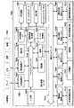
図5は、固体撮像素子20における受光素子200として備えられる画素からの信号の出力の一例として、カラムごとに信号を出力する例を模式的に示す図である。カラムごとにAD変換をする例について示す。受光素子200は、その内部に画素206をカラム方向及びライン方向にアレイ状に備える画素アレイを有する。
水平方向制御部208は、画素アレイにおける画素のラインを選択する回路である。水平方向制御部208からの制御信号に基づいて、受光素子200における画素206のラインが選択され、選択されたラインに属する画素から画素信号(アナログ信号)が出力される。
コンパレータ210は、カラムごとに出力される画素からのアナログ信号を、例えば、デジタル信号をDA変換によりアナログ信号へと変換したランプ信号と比較し、その比較結果を増幅して、カラムごとに出力する。
カウンタ212は、コンパレータ210からの出力に基づいて、それぞれの画素206から出力される画素値をデジタル信号として出力する。
上記は一般的な構成であるが、本実施形態における固体撮像素子20はさらに、カラム電源制御部214を備える。カラム電源制御部214は、コンパレータ210において、カラムごとに備えられる比較回路の電源電圧を制御する回路である。このカラム電源制御部214によりカラムごとに局所的に電源電圧を制御することにより、本実施形態の固体撮像素子20は、適切なディザ処理を実現する。
図6は、本実施形態に係る固体撮像素子20におけるコンパレータ210と、カラムごとの局所電源を制御するカラム電源制御部214の一例を示す図である。以下の例においては、例えば、局所電源電圧を3通りにして、ディザ処理を実行するものである。3通りの電圧は、限定されない一例として示すものであり、局所電源の電圧は、2通りであってもよいし、4通り以上であってもよい。
コンパレータ210は、カラムごとにカラム比較回路210A、210B、210C、・・・、を備える。添え字のA、B、Cは、カラムを識別する文字である。それぞれのカラム比較回路は、同一の回路で構成されることが望ましい。ここでは、カラム比較回路210Aを例に構成を説明する。
カラム比較回路210Aは、キャパシタC1、C2、C3と、トランジスタM1、M2、M3、M4と、スイッチSW1、SW2と、否定回路N1と、を備える。
キャパシタC1、C2は、オートゼロ容量を構成する。キャパシタC1は、一端がカラムごとの垂直信号線VSLに接続される。キャパシタC2は、一端にランプ信号Rampが入力される。キャパシタC1、C2のそれぞれの他端は接続され、画素からの信号をランプ信号Rampに重畳して信号DIFFDACを出力する。
トランジスタM1は、例えば、p型のMOSFET(Metal-Oxide-Semiconductor Field-Effect Transistor)であり、ソースがカラム電源制御部214に接続され電源電圧VDDAが印加され、ゲートがキャパシタC1、C2と接続されてDIFFDACが印加される。
トランジスタM2は、例えば、n型のMOSFETであり、ドレインがトランジスタM1のドレインと接続され、ソースが電源電圧VSSに接続される。このトランジスタM2は、第1電流源として動作する。トランジスタM2のゲートには、適切なバイアス電圧が印加され、ドレインの電位に基づいたドレイン電流を流す。
トランジスタM1、M2のドレイン間において、信号VOUT1をトランジスタM3のゲートへと出力する。
スイッチSW1は、トランジスタM1のゲートとドレインの間に接続される。スイッチSW1は、オートゼロ信号AZPにより、トランジスタM1のゲートとドレイン間の短絡及び開放を制御する。スイッチSW1がオンすることにより、トランジスタM1のゲートは、トランジスタM2を介して電源電圧VSSに接続され、キャパシタC1、C2の電荷をリセットする。
トランジスタM3は、例えば、p型のMOSFETであり、ソースがカラム電源制御部214に接続され電源電圧VDDAが印加され、ゲートがトランジスタM1のドレインと接続される。
トランジスタM4は、例えば、n型のMOSFETであり、ドレインがトランジスタM3のドレインと接続され、ゲートがキャパシタC3の一端と接続され、ソースが電源電圧VSSと接続される。このトランジスタM4は、第2電流源として動作する。
トランジスタM3、M4のドレイン間において、信号VOUT2を否定回路N1へと出力する。
キャパシタC3は、第2電流源として動作するトランジスタM4のゲートの電位を生成するキャパシタである。
スイッチSW2は、トランジスタM4のゲートとドレインとの間に接続される。スイッチSW1は、オートゼロ信号AZNにより、トランジスタM4のゲートとドレイン間の短絡及び開放を制御する。スイッチSW2がオンすることにより、トランジスタM4のゲートは、ドレインと接続され、ゲートの電位をリセットする。
否定回路N1は、入力を反転して出力する回路であり、入力されたVOUT2を反転して、コンパレータからの出力信号OUTを出力する。なお、構成によっては、否定回路N1の前後において、クランプ回路が接続されていてもよい。このクランプ回路は、コンパレータから選択的に出力することができる回路であってもよい。
この回路は、一例として挙げられる回路であり、カラムに対するコンパレータの回路は、この図6の例に限定されるものではない。
カラム電源制御部214は、セレクタ216と、局所電源218A、218B、218C、・・・、を備える。カラム電源制御部214は、各カラムに対応するカラム比較回路210A、210B、210C、・・・、に適切な電源電圧を印加し、ディザ効果を発生させる回路である。
セレクタ216は、制御信号Cntと、局所電源となる電圧V1、V2、V3と、が入力され、適切な出力先に適切な電圧を出力する回路である。セレクタ216は、制御信号Cntにしたがって、どのカラムにどの電圧を出力するかを選択する。
局所電源218Aは、カラム比較回路210Aに対する電源電圧を制御し、出力する回路である。局所電源218Aは、電源電圧VDDに接続され、セレクタ216から出力された電圧を安定した電圧に制御して、カラム比較回路210Aの電源端子へ電源電圧VDDAを出力する。カラムA以外の他のカラムについても同様である。局所電源218は、それぞれが、例えば、LDO(Low Dropout)等のレギュレータを備えて構成されてもよい。局所電源218は、複数の電圧値に対して安定した電圧を出力するレギュレータ、例えば、入出力電圧にある程度の幅を有していても適切に安定した電圧を供給できるレギュレータを用いることが望ましい。
例えば、制御信号Cntとして、カラム比較回路210Aの電源電圧をV1に設定する信号が入力されると、セレクタ216は、局所電源218Aに電源電圧V1を接続する。局所電源218Aは、入力された電圧を安定した電圧V1へと変換して、カラム比較回路210Aへと電源電圧として出力する。
図7は、セレクタ216の限定されない一例を示す回路図である。セレクタ216は、抵抗R1、R2、R3、R4と、電流源I1と、スイッチSW1A、SW1B、SW1C、SW2A、SW2B、SW2C、SW3A、SW3B、SW3Cと、を備える。
抵抗R1、R2、R3、R4と、電流源I1は、電源電圧VDD、VSSの間に直列に接続される。これらの抵抗と電流源により、抵抗同士の接点において異なる電圧を生成する。例えば、抵抗R1、R2の節点の電位がV1、抵抗R2、R3の節点の電位がV2、抵抗R3、R4の節点の電位がV3であるとする。
スイッチSW1A、SW2A、SW3Aは、制御信号Cntにより、排他的に制御される。同様に、スイッチSW1B、SW2B、SW3B、及び、スイッチSW1C、SW2C、SW3Cは、それぞれ排他的に制御される。
図7の例においては、スイッチSW1A、SW2B、SW3Cがオンし、それ以外のスイッチがオフしている。このようなスイッチの接続においては、電圧V1が局所電源218Aに出力され、電圧V2が局所電源218Bに出力され、電圧V3が局所電源218Cに出力される。
以上のような構成により、制御信号Cntに基づいて、カラムのコンパレータに対して、それぞれ制御された電源電圧を印加することが可能となる。
図8は、図7のようにセレクタ216が接続されている場合におけるタイミングチャートである。実線、点線、破線がある組み合わせについて、実線は、電源電圧V1及びV1が選択されたカラムの入出力を表し、点線は、V2及びV2が選択されたカラムの入出力を表し、破線は、V3及びV3が選択されたカラムの入出力を表す。
まず、AZP、AZNがオンしていることにより、カラム比較回路210A、210B、210C、・・・は、リセットされている状態である。この状態において、カラム電源制御部214により、電圧V1、V2、V3が制御される。この期間において、カラム比較回路210A等におけるそれぞれのキャパシタがそれぞれのカラムに印加される電源電圧V1、V2、V3に基づいて適切にリセットレベルに設定される。
画素信号の読み取り準備状態になると、AZP、AZNがオフする。続いて、V1~V3をリセットすることにより、VDDA、VDDB、VDDCがリセットレベルへと遷移する。例えば、図8の例のように、V1、V3をV2と同等の電圧としてもよい。なお、V2とする必要は無く、ADを実行するタイミングにおいて、同一の電位となるように制御すればよい。
その後ランプ信号Rampが適切に印加されることにより、画素値、及び、キャパシタのリセットレベルに基づいたタイミングで、VOUT1が出力される。このVOUT1によりトランジスタM3のゲート電位が変化することで、VOUT1の遷移タイミングに基づいた信号がそれぞれのカラム比較回路210A等から出力される。
このように、V1、V2、V3の電圧の差により、OUTを出力するタイミングをずらすことができ、ディザ処理を適切に実行することができる。
次に、セレクタ216における電源電圧の選択について説明する。
図9は、カラム電源制御部214による制御の限定されない一例を示す表である。この図に示すように、3つのカラムに対して、3つの電源電圧を順番に適用してもよい。この例に示すように、周期的にカラムに付与する電源電圧を制御してもよい。このように電源電圧を変化させることにより、同じタイミングにおいては、カラム方向にディザ処理を実行することができるとともに、ADごとに同じカラムにおいて時間方向のディザ処理を実行することが可能となる。
なお、図9においては、周期的な電源電圧の変化となっているが、これには限られず、乱数により電源電圧が変化してもよい。また、乱数は、一様乱数には限られず、例えば、正規分布、ポアッソン分布、二項分布等に基づいた乱数としてもよい。乱数を用いる場合、各カラムに異なる乱数を用いてもよいし、上記と同様に、カラムAとカラムDは、同じ電源電圧とするようなカラム方向に対する周期性を有していてもよい。すなわち、カラムAに印加される電圧は、ランダムに決定されるが、カラムAとカラムDは、常に同じ電源電圧が印加されるとしてもよい。
このように、セレクタ216により入出力の関係をADごとに変化させてもよい。セレクタ216によりADごとに同一カラムに印加するバイス電圧を変化させることにより、同一カラムにおけるP相の出力タイミングを時間方向に変化させることができる。
図10は、カラム電源制御部214による制御の限定されない他の一例を示す表である。この図に示すように、3つのカラムに対して時間によらず3つの電源電圧を適用してもよい。この場合、図9に示すように、時間方向のディザ処理は実現できないものの、カラム方向に対してのディザ処理を適切に実行することが可能となる。
特に、隣接するカラム同士には、異なる電源電圧が印加されるように制御してもよい。また、取り合うカラムに限られず、所定値(例えば、3カラム以上)等に連続して同じ電源電圧が印加されないように、カラム方向に乱数により印加する電圧を決定してもよい。
以上のように、本実施形態によれば、カラムごとに異なる電源電圧をコンパレータの電源電圧として印加することにより、カラム方向及び時間方向にディザ効果を適切に発生させることが可能となる。このように処理することで、P相のカウントを増加させることなく、画像信号において適切にディザ効果を発生させることが可能となる。また、ミスマッチによらないディザの付与が可能であり、トランジスタのサイズ等の設計自由度を増すことができる。また、P相におけるランプ信号の制御をすることなく、適切にP相におけるカウントを制御することが可能となる。
なお、前述において説明したように、セレクタ216により選択される信号の種類及び信号を振り分けるカラムの周期は、3に限られるものではない。例えば、セレクタ216は、n (n >= 2)種類の電源電圧を、m (m >= 2)カラム周期で振り分けることも可能である。この場合、セレクタ216には、電源電圧の入力としてn本の種類の電位が入力される入力線を備え、又は、セレクタ216においてn種類の電位が設定できる電源を備える。そして、セレクタ216は、n種類の電源電圧を適切にm種類のカラムに選択的に出力できるような回路構成を有する。
例えば、図7においては、n = 3 (V1, V2, V3)、m = 3 (218A, 218B, 218C)である。そして、カラム電源制御部214は、n種類の電位が生成可能である回路と、n本の制御線の接続関係とを制御可能な選択回路とを備える。このn本の制御線は、例えば、mカラム周期で、各カラムに対応する局所電源手段に接続される。
(第2実施形態)
図11は、第2実施形態に係るカラム電源制御部214の一例を示す回路図である。前述の実施形態の構成に加え、さらに、隣接するカラムの電源電圧端子を短絡するためのスイッチが配置されている。
図11は、第2実施形態に係るカラム電源制御部214の一例を示す回路図である。前述の実施形態の構成に加え、さらに、隣接するカラムの電源電圧端子を短絡するためのスイッチが配置されている。
例えば、カラムA、B間の電源電圧を印加する線の間には、スイッチSWabが配置され、カラムB、C間においては、スイッチSWbcが配置されている。これらのスイッチは、制御信号Cntswにより制御される。
カラム電源制御部214は、さらに、この制御信号Cntswを出力するスイッチ制御回路(図示しない)を備えていてもよい。
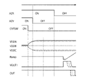
図12は、図11のようにセレクタ216が接続されている場合におけるタイミングチャートである。この図12に示すように、制御信号Cntswを、AZP及びAZNがオンからオフに切り替える前にオンからオフに切り替える。このタイミングは、VDDA等が立ち上がり、立ち下がりをしきる前にオートゼロがオフとなるようなタイミングに設定される。すなわち、図の一点鎖線で表されるような電源電圧において、カラムごとにキャパシタがリセットされる。
このような電源電圧が印加されるので、前述の実施形態と同様に、各カラムに対する比較回路からの出力タイミングにずれを生じさせる。
以上のように、本実施形態によっても、カラムごとに付与される電源電圧を変動させる制御をすることが可能となる。この変動分をAD変換のリセットレベルに重畳することにより、P相におけるカウントにばらつきを付与することが可能となる。本実施形態では、ディザ量を、AZとCntswのタイミングにより制御することができる。また、カラム間で電源電位を短絡させ、その後に変動させるため、短絡されたカラム同士は、平均化した電位を起点にVthのミスマッチ分ばらつく。この結果、電源電圧の平均値自体は、変動がない。
図13は、本実施形態に係るAZPと、Cntswのタイミングによるディザ効果の大きさの関係を示す図である。上記にAZの前にCntswをオンからオフにするとしたが、これには限られない。例えば、AZPを先にオフにし、その後にCntswをオンにしてもよい。また、AZPと同時にCntswをオンにしてもよい。例えば、V1が短絡されているカラムにおける平均の電源電圧よりも高い場合には、V1と接続されているカラムAの電源電位は、図13のV1に示すような遷移をする。この状態でtadからAD変換が開始されたとする。
t1においてAZPがオフとなっている場合、リセット時とAD変換時におけるVDDAの差がt2~t5と比較して大きくなるため、ディザ量が大きくなる。一方で、t5においてAZPがオフとなっている場合、リセット時とAD変換時におけるVDDAの差がt1~t3と比較して小さくなるため、ディザ量が大きくなる。このように、AZPの切替タイミング、又は、Cntswの切替タイミングにより、ディザ量を制御することも可能となる。
このように、AZP、Cntswのタイミングを制御することで、前述の実施形態における時間方向のディザと同様のディザ処理を実現することもできる。別の例としては、AD変換ごとに、ディザをする/しないを切り替えてもよい。例えば、Cntswをオフのまま制御することにより、隣接するカラムにおいて、ディザ処理がされないこととなる。これをAD変換ごとに切り替えることにより、時間方向にディザ処理をすることが可能となる。
図14は、オンからオフへの立ち下がりのタイミングの異なるCntswを生成する回路である。制御信号は、マルチプレクサMUXに複数の入力信号のいずれを選ぶかを制御する選択信号である。
マルチプレクサMUXには、異なる個数のバッファを経由したそれぞれの立ち下がりのタイミングが異なる信号が入力される。この立ち下がりのタイミングが異なる信号のうち、所望の信号を制御信号によりマルチプレクサMUXから出力することにより、図13のようにタイミングでディザ量を制御する場合に所望の信号を出力させることができる。この回路ももちろん、カラム電源制御部214に備えられてもよい。点線が入力されたパルスのタイミングであり、各バッファにより、異なるタイミングの実線で示す立ち下がりパルスが出力される。
制御信号は、前述の実施形態と同様に、周期的にそれぞれのカラムに適切なリセットレベルを設定するように設定されてもよいし、ADごとに乱数等により設定が更新されるものであってもよい。
図15は、オンからオフの立ち下がりのタイミングの異なるCntswを仮想的に生成する回路である。制御信号は、図14の場合と同様であり、周期的であってもよいし、ランダムであってもよい。
図15の回路は、マルチプレクサMUXに入力されるバッファの駆動能力が異なる。この駆動能力の違いにより、例えば、各バッファの出力は、バッファの右上に示すように、駆動能力が高いほど鋭い信号を、駆動能力が低いほどなまった信号を出力する。この信号を制御信号により、適切にマルチプレクサMUXから出力する。
このような立ち下がりのスロープが異なる信号をCntswとすることで、スイッチSWab等がオフとなる閾値電圧を下回るタイミングをずらすことにより、ディザ量を制御することができる。
図16は、時間方向のディザを行う短絡、開放を制御する別の例を示す表である。同じ矢印が属するカラム同士が、各AD変換において短絡、開放の対象となるカラムである。このように、AD変換処理ごとに、短絡、開放をするカラム同士を変更してもよい。この図16においては、周期的にカラムの接続関係が制御されているが、カラムの接続関係は、周期的ではなく、ランダムに制御されてもよい。例えば、ランダムウォークのように、左右いずれかに接続関係をずらす(図14における矢印の位置を左右に動かすか、又は、動かさないかのいずれかから選択する)制御としてもよい。
(第3実施形態)
前述の各実施形態は、各カラムの比較回路として、差動動作しないものを選択していたが、これに限られるものではない。例えば、ランプ信号と画素からの信号を差動信号に基づいて比較を実現する回路であっても本開示の手法を適用することができる。
前述の各実施形態は、各カラムの比較回路として、差動動作しないものを選択していたが、これに限られるものではない。例えば、ランプ信号と画素からの信号を差動信号に基づいて比較を実現する回路であっても本開示の手法を適用することができる。
図17は、本実施形態におけるカラム比較回路210Aを示した回路図である。カラム比較回路210Aは、ランプ信号Rampと、画素からの垂直信号線VSLからの信号を差動入力として受け付け、この信号の差に基づいて、カウンタ回路におけるタイミング信号を取得する。なお、この回路は、差動アンプを用いるコンパレータの限定されない一例としてあげたものであり、この他の回路においても同様に適用することができる。
スイッチSWr、SWvは、例えば、図に示すように、下段に設置されるそれぞれの信号の入力端となるn型のMOSFETのゲートとドレインとの間に接続される。オートゼロ信号AZR、AZVにより、それぞれの入力トランジスタが適切にリセットされる。
一般的には、このような差動アンプ型においては、AZRとAZVは、同時にオン/オフが切り替えられるが、本実施形態においては、このタイミングをずらすことにより、前述の第1実施形態と同様のディザ効果を得ることができる。
図18は、本実施形態におけるタイミングチャートの一例を示す図である。この図18に示すように、まず、V1等の制御をする前に、AZVをオフさせて、画素からの信号が入力されるトランジスタのリセット状態を解除する。
続いて、V1等を制御することにより、ランプ信号側のキャパシタのリセットレベルを変動させる。
そして、VDDA等が定常状態に遷移下の地に、AZRをオフして、ランプ信号入力側のトランジスタのリセット状態を解除する。
このように制御することで、画素からの信号を受信するリセットレベルと、ランプ信号を受信するリセットレベルとを変動させることにより、ディザ効果を発揮することが可能となる。
図19は、第2実施形態の比較回路を差動入力型としたものである。カラム間を短絡、開放するスイッチがある以外は、図17と同様の構成である。すなわち、差動入力を受け付けるコンパレータとして限定されない一例として提示するものである。
図20は、図19の場合におけるタイミングチャートを示す図である。この場合も同様に、Cntswをオフした後に、まず、AZVをオフして、画素側のトランジスタのリセットレベルを設定する。この後に、ランプ信号側の入力トランジスタのリセットレベルを設定する。
このように制御することで、リセットレベルを変動させ、第2実施形態と同様に、適切なディザ処理を実現することが可能となる。
本開示に係る技術(本技術)は、様々な製品へ応用することができる。例えば、本開示に係る技術は、自動車、電気自動車、ハイブリッド電気自動車、自動二輪車、自転車、パーソナルモビリティ、飛行機、ドローン、船舶、ロボット等のいずれかの種類の移動体に搭載される装置として実現されてもよい。
図21は、本開示に係る技術が適用され得る移動体制御システムの一例である車両制御システムの概略的な構成例を示すブロック図である。
車両制御システム12000は、通信ネットワーク12001を介して接続された複数の電子制御ユニットを備える。図21に示した例では、車両制御システム12000は、駆動系制御ユニット12010、ボディ系制御ユニット12020、車外情報検出ユニット12030、車内情報検出ユニット12040、及び統合制御ユニット12050を備える。また、統合制御ユニット12050の機能構成として、マイクロコンピュータ12051、音声画像出力部12052、及び車載ネットワークI/F(Interface)12053が図示されている。
駆動系制御ユニット12010は、各種プログラムにしたがって車両の駆動系に関連する装置の動作を制御する。例えば、駆動系制御ユニット12010は、内燃機関又は駆動用モータ等の車両の駆動力を発生させるための駆動力発生装置、駆動力を車輪に伝達するための駆動力伝達機構、車両の舵角を調節するステアリング機構、及び、車両の制動力を発生させる制動装置等の制御装置として機能する。
ボディ系制御ユニット12020は、各種プログラムにしたがって車体に装備された各種装置の動作を制御する。例えば、ボディ系制御ユニット12020は、キーレスエントリシステム、スマートキーシステム、パワーウィンドウ装置、あるいは、ヘッドランプ、バックランプ、ブレーキランプ、ウィンカー又はフォグランプ等の各種ランプの制御装置として機能する。この場合、ボディ系制御ユニット12020には、鍵を代替する携帯機から発信される電波又は各種スイッチの信号が入力され得る。ボディ系制御ユニット12020は、これらの電波又は信号の入力を受け付け、車両のドアロック装置、パワーウィンドウ装置、ランプ等を制御する。
車外情報検出ユニット12030は、車両制御システム12000を搭載した車両の外部の情報を検出する。例えば、車外情報検出ユニット12030には、撮像部12031が接続される。車外情報検出ユニット12030は、撮像部12031に車外の画像を撮像させるとともに、撮像された画像を受信する。車外情報検出ユニット12030は、受信した画像に基づいて、人、車、障害物、標識又は路面上の文字等の物体検出処理又は距離検出処理を行ってもよい。
撮像部12031は、光を受光し、その光の受光量に応じた電気信号を出力する光センサである。撮像部12031は、電気信号を画像として出力することもできるし、測距の情報として出力することもできる。また、撮像部12031が受光する光は、可視光であっても良いし、赤外線等の非可視光であっても良い。
車内情報検出ユニット12040は、車内の情報を検出する。車内情報検出ユニット12040には、例えば、運転者の状態を検出する運転者状態検出部12041が接続される。運転者状態検出部12041は、例えば運転者を撮像するカメラを含み、車内情報検出ユニット12040は、運転者状態検出部12041から入力される検出情報に基づいて、運転者の疲労度合い又は集中度合いを算出してもよいし、運転者が居眠りをしていないかを判別してもよい。
マイクロコンピュータ12051は、車外情報検出ユニット12030又は車内情報検出ユニット12040で取得される車内外の情報に基づいて、駆動力発生装置、ステアリング機構又は制動装置の制御目標値を演算し、駆動系制御ユニット12010に対して制御指令を出力することができる。例えば、マイクロコンピュータ12051は、車両の衝突回避あるいは衝撃緩和、車間距離に基づく追従走行、車速維持走行、車両の衝突警告、又は車両のレーン逸脱警告等を含むADAS(Advanced Driver Assistance System)の機能実現を目的とした協調制御を行うことができる。
また、マイクロコンピュータ12051は、車外情報検出ユニット12030又は車内情報検出ユニット12040で取得される車両の周囲の情報に基づいて駆動力発生装置、ステアリング機構又は制動装置等を制御することにより、運転者の操作に拠らずに自律的に走行する自動運転等を目的とした協調制御を行うことができる。
また、マイクロコンピュータ12051は、車外情報検出ユニット12030で取得される車外の情報に基づいて、ボディ系制御ユニット12030に対して制御指令を出力することができる。例えば、マイクロコンピュータ12051は、車外情報検出ユニット12030で検知した先行車又は対向車の位置に応じてヘッドランプを制御し、ハイビームをロービームに切り替える等の防眩を図ることを目的とした協調制御を行うことができる。
音声画像出力部12052は、車両の搭乗者又は車外に対して、視覚的又は聴覚的に情報を通知することが可能な出力装置へ音声及び画像のうちの少なくとも一方の出力信号を送信する。図21の例では、出力装置として、オーディオスピーカ12061、表示部12062及びインストルメントパネル12063が例示されている。表示部12062は、例えば、オンボードディスプレイ及びヘッドアップディスプレイの少なくとも一つを含んでいてもよい。
図22は、撮像部12031の設置位置の例を示す図である。
図22では、撮像部12031として、撮像部12101、12102、12103、12104、12105を有する。
撮像部12101、12102、12103、12104、12105は、例えば、車両12100のフロントノーズ、サイドミラー、リアバンパ、バックドア及び車室内のフロントガラスの上部等の位置に設けられる。フロントノーズに備えられる撮像部12101及び車室内のフロントガラスの上部に備えられる撮像部12105は、主として車両12100の前方の画像を取得する。サイドミラーに備えられる撮像部12102、12103は、主として車両12100の側方の画像を取得する。リアバンパ又はバックドアに備えられる撮像部12104は、主として車両12100の後方の画像を取得する。車室内のフロントガラスの上部に備えられる撮像部12105は、主として先行車両又は、歩行者、障害物、信号機、交通標識又は車線等の検出に用いられる。
なお、図22には、撮像部12101ないし12104の撮影範囲の一例が示されている。撮像範囲12111は、フロントノーズに設けられた撮像部12101の撮像範囲を示し、撮像範囲12112,12113は、それぞれサイドミラーに設けられた撮像部12102,12103の撮像範囲を示し、撮像範囲12114は、リアバンパ又はバックドアに設けられた撮像部12104の撮像範囲を示す。例えば、撮像部12101ないし12104で撮像された画像データが重ね合わせられることにより、車両12100を上方から見た俯瞰画像が得られる。
撮像部12101ないし12104の少なくとも1つは、距離情報を取得する機能を有していてもよい。例えば、撮像部12101ないし12104の少なくとも1つは、複数の撮像素子からなるステレオカメラであってもよいし、位相差検出用の画素を有する撮像素子であってもよい。
例えば、マイクロコンピュータ12051は、撮像部12101ないし12104から得られた距離情報を基に、撮像範囲12111ないし12114内における各立体物までの距離と、この距離の時間的変化(車両12100に対する相対速度)を求めることにより、特に車両12100の進行路上にある最も近い立体物で、車両12100と略同じ方向に所定の速度(例えば、0km/h以上)で走行する立体物を先行車として抽出することができる。さらに、マイクロコンピュータ12051は、先行車の手前に予め確保すべき車間距離を設定し、自動ブレーキ制御(追従停止制御も含む)や自動加速制御(追従発進制御も含む)等を行うことができる。このように運転者の操作に拠らずに自律的に走行する自動運転等を目的とした協調制御を行うことができる。
例えば、マイクロコンピュータ12051は、撮像部12101ないし12104から得られた距離情報を元に、立体物に関する立体物データを、2輪車、普通車両、大型車両、歩行者、電柱等その他の立体物に分類して抽出し、障害物の自動回避に用いることができる。例えば、マイクロコンピュータ12051は、車両12100の周辺の障害物を、車両12100のドライバが視認可能な障害物と視認困難な障害物とに識別する。そして、マイクロコンピュータ12051は、各障害物との衝突の危険度を示す衝突リスクを判断し、衝突リスクが設定値以上で衝突可能性がある状況であるときには、オーディオスピーカ12061や表示部12062を介してドライバに警報を出力することや、駆動系制御ユニット12010を介して強制減速や回避操舵を行うことで、衝突回避のための運転支援を行うことができる。
撮像部12101ないし12104の少なくとも1つは、赤外線を検出する赤外線カメラであってもよい。例えば、マイクロコンピュータ12051は、撮像部12101ないし12104の撮像画像中に歩行者が存在するか否かを判定することで歩行者を認識することができる。かかる歩行者の認識は、例えば赤外線カメラとしての撮像部12101ないし12104の撮像画像における特徴点を抽出する手順と、物体の輪郭を示す一連の特徴点にパターンマッチング処理を行って歩行者か否かを判別する手順によって行われる。マイクロコンピュータ12051が、撮像部12101ないし12104の撮像画像中に歩行者が存在すると判定し、歩行者を認識すると、音声画像出力部12052は、当該認識された歩行者に強調のための方形輪郭線を重畳表示するように、表示部12062を制御する。また、音声画像出力部12052は、歩行者を示すアイコン等を所望の位置に表示するように表示部12062を制御してもよい。
以上、本開示に係る技術が適用され得る車両制御システムの一例について説明した。本開示に係る技術は、以上説明した構成のうち、撮像部12031に適用され得る。具体的には、図1等の固体撮像装置、図5等の固体撮像素子は、撮像部12031に適用することができる。
前述した実施形態は、以下のような形態としてもよい。
(1)
受光した光を光電変換して信号を出力する画素がアレイ状に備えられる、画素アレイと、
前記画素アレイのラインを選択し、前記ラインに属する前記画素からの信号出力を制御する、水平方向制御部と、
前記画素アレイのカラムごとに前記画素からの出力信号を比較する複数のカラム比較回路を備える、コンパレータと、
前記カラム比較回路のそれぞれに対する電源電圧を制御する、カラム電源制御部と、
を備える固体撮像素子。
受光した光を光電変換して信号を出力する画素がアレイ状に備えられる、画素アレイと、
前記画素アレイのラインを選択し、前記ラインに属する前記画素からの信号出力を制御する、水平方向制御部と、
前記画素アレイのカラムごとに前記画素からの出力信号を比較する複数のカラム比較回路を備える、コンパレータと、
前記カラム比較回路のそれぞれに対する電源電圧を制御する、カラム電源制御部と、
を備える固体撮像素子。
(2)
前記カラム電源制御部は、n (n >= 2)種類の電源電圧を前記カラム比較回路のそれぞれに印加する、
(1)に記載の固体撮像素子。
前記カラム電源制御部は、n (n >= 2)種類の電源電圧を前記カラム比較回路のそれぞれに印加する、
(1)に記載の固体撮像素子。
(3)
前記カラム電源制御部は、n種類の電位が生成可能な回路を備える、
(2)に記載の固体撮像素子。
前記カラム電源制御部は、n種類の電位が生成可能な回路を備える、
(2)に記載の固体撮像素子。
(4)
前記カラム電源制御部は、n種類の電位を伝達するn本の制御線を備える、
(3)に記載の固体撮像素子。
前記カラム電源制御部は、n種類の電位を伝達するn本の制御線を備える、
(3)に記載の固体撮像素子。
(5)
前記カラム電源制御部は、m (m >= 2)個の前記カラム比較回路ごとに、同じ電源電圧を印加する、
(4)に記載の固体撮像素子。
前記カラム電源制御部は、m (m >= 2)個の前記カラム比較回路ごとに、同じ電源電圧を印加する、
(4)に記載の固体撮像素子。
(6)
前記カラム電源制御部は、n本の制御線をmカラム周期で前記カラム比較回路と接続させる、セレクタ、を備える、
(5)に記載の固体撮像素子。
前記カラム電源制御部は、n本の制御線をmカラム周期で前記カラム比較回路と接続させる、セレクタ、を備える、
(5)に記載の固体撮像素子。
(7)
前記セレクタは、AD変換ごとに、n本の制御線とm周期の前記カラム比較回路との接続状況を遷移させる、
(6)に記載の固体撮像素子。
前記セレクタは、AD変換ごとに、n本の制御線とm周期の前記カラム比較回路との接続状況を遷移させる、
(6)に記載の固体撮像素子。
(8)
前記セレクタは、時間に対する周期的に、AD変換ごとの接続状況を遷移させる、
(7)に記載の固体撮像素子。
前記セレクタは、時間に対する周期的に、AD変換ごとの接続状況を遷移させる、
(7)に記載の固体撮像素子。
(9)
前記セレクタは、乱数に基づいて、AD変換ごとの接続状況を遷移させる、
(7)に記載の固体撮像素子。
前記セレクタは、乱数に基づいて、AD変換ごとの接続状況を遷移させる、
(7)に記載の固体撮像素子。
(10)
前記から無電源制御部は、n本の制御線に対して、
前記カラム比較回路のリセットのタイミングにおいては、n種類の電位を出力し、
AD変換のタイミングにおいては、1種類の電位を出力する、
(2)から(9)のいずれかに記載の固体撮像素子。
前記から無電源制御部は、n本の制御線に対して、
前記カラム比較回路のリセットのタイミングにおいては、n種類の電位を出力し、
AD変換のタイミングにおいては、1種類の電位を出力する、
(2)から(9)のいずれかに記載の固体撮像素子。
(11)
前記カラム電源制御部は、前記カラム比較回路に電源電圧を印加する電源線について、他の前記カラム比較回路の前記電源線との短絡、開放を制御する、スイッチと、
前記スイッチの切替状態を制御するスイッチ制御信号を発信する、スイッチ制御回路と、
を備える、
(1)に記載の固体撮像素子。
前記カラム電源制御部は、前記カラム比較回路に電源電圧を印加する電源線について、他の前記カラム比較回路の前記電源線との短絡、開放を制御する、スイッチと、
前記スイッチの切替状態を制御するスイッチ制御信号を発信する、スイッチ制御回路と、
を備える、
(1)に記載の固体撮像素子。
(12)
前記カラム電源制御部は、前記カラム比較回路のリセットのタイミングと、AD変換のタイミングと、において、それぞれの前記カラム比較回路の電源電圧を変動させる、
(11)に記載の固体撮像素子。
前記カラム電源制御部は、前記カラム比較回路のリセットのタイミングと、AD変換のタイミングと、において、それぞれの前記カラム比較回路の電源電圧を変動させる、
(11)に記載の固体撮像素子。
(13)
前記カラム電源制御部は、前記カラム比較回路のAD変換ごとに、電源電圧を変動させるか、させないかを制御する、
(11)に記載の固体撮像素子。
前記カラム電源制御部は、前記カラム比較回路のAD変換ごとに、電源電圧を変動させるか、させないかを制御する、
(11)に記載の固体撮像素子。
(14)
前記カラム電源制御部は、AD変換ごとに、前記スイッチを制御し、短絡する前記カラム比較回路の組み合わせを変動させる、
(11)に記載の固体撮像素子。
前記カラム電源制御部は、AD変換ごとに、前記スイッチを制御し、短絡する前記カラム比較回路の組み合わせを変動させる、
(11)に記載の固体撮像素子。
(15)
前記画素における受講環境を制御する、光学系と、
(1)から(14)のいずれかに記載の固体撮像素子と、
前記固体撮像素子から出力される信号を処理する、処理回路と、
を備える、固体撮像装置。
前記画素における受講環境を制御する、光学系と、
(1)から(14)のいずれかに記載の固体撮像素子と、
前記固体撮像素子から出力される信号を処理する、処理回路と、
を備える、固体撮像装置。
本開示の態様は、前述した実施形態に限定されるものではなく、想到しうる種々の変形も含むものであり、本開示の効果も前述の内容に限定されるものではない。各実施形態における構成要素は、適切に組み合わされて適用されてもよい。すなわち、特許請求の範囲に規定された内容及びその均等物から導き出される本開示の概念的な思想と趣旨を逸脱しない範囲で種々の追加、変更及び部分的削除が可能である。
1: 固体撮像装置、
10: 光学系、
12: 電源部、
14: 操作部、
16: 制御部、
18: 表示部、
20: 固体撮像素子、
22: 記憶部、
24: 処理部、
200: 受光素子、
202: 記憶回路、
204: 処理回路、
206: 画素、
208: 水平方向制御部、
210: コンパレータ、
212: カウンタ、
214: カラム電源制御部、
216: セレクタ、
218: 局所電源、
10: 光学系、
12: 電源部、
14: 操作部、
16: 制御部、
18: 表示部、
20: 固体撮像素子、
22: 記憶部、
24: 処理部、
200: 受光素子、
202: 記憶回路、
204: 処理回路、
206: 画素、
208: 水平方向制御部、
210: コンパレータ、
212: カウンタ、
214: カラム電源制御部、
216: セレクタ、
218: 局所電源、
Claims (15)
- 受光した光を光電変換して信号を出力する画素がアレイ状に備えられる、画素アレイと、
前記画素アレイのラインを選択し、前記ラインに属する前記画素からの信号出力を制御する、水平方向制御部と、
前記画素アレイのカラムごとに前記画素からの出力信号を比較する複数のカラム比較回路を備える、コンパレータと、
前記カラム比較回路のそれぞれに対する電源電圧を制御する、カラム電源制御部と、
を備える固体撮像素子。 - 前記カラム電源制御部は、n (n >= 2)種類の電源電圧を前記カラム比較回路のそれぞれに印加する、
請求項1に記載の固体撮像素子。 - 前記カラム電源制御部は、n種類の電位が生成可能な回路を備える、
請求項2に記載の固体撮像素子。 - 前記カラム電源制御部は、n種類の電位を伝達するn本の制御線を備える、
請求項3に記載の固体撮像素子。 - 前記カラム電源制御部は、m (m >= 2)個の前記カラム比較回路ごとに、同じ電源電圧を印加する、
請求項4に記載の固体撮像素子。 - 前記カラム電源制御部は、n本の制御線をmカラム周期で前記カラム比較回路と接続させる、セレクタ、を備える、
請求項5に記載の固体撮像素子。 - 前記セレクタは、AD変換ごとに、n本の制御線とm周期の前記カラム比較回路との接続状況を遷移させる、
請求項6に記載の固体撮像素子。 - 前記セレクタは、時間に対する周期的に、AD変換ごとの接続状況を遷移させる、
請求項7に記載の固体撮像素子。 - 前記セレクタは、乱数に基づいて、AD変換ごとの接続状況を遷移させる、
請求項7に記載の固体撮像素子。 - 前記カラム電源制御部は、n本の制御線に対して、
前記カラム比較回路のリセットのタイミングにおいては、n種類の電位を出力し、
AD変換のタイミングにおいては、1種類の電位を出力する、
請求項2に記載の固体撮像素子。 - 前記カラム電源制御部は、前記カラム比較回路に電源電圧を印加する電源線について、他の前記カラム比較回路の前記電源線との短絡、開放を制御する、スイッチと、
前記スイッチの切替状態を制御するスイッチ制御信号を発信する、スイッチ制御回路と、
を備える、
請求項1に記載の固体撮像素子。 - 前記カラム電源制御部は、前記カラム比較回路のリセットのタイミングと、AD変換のタイミングと、において、それぞれの前記カラム比較回路の電源電圧を変動させる、
請求項11に記載の固体撮像素子。 - 前記カラム電源制御部は、前記カラム比較回路のAD変換ごとに、電源電圧を変動させるか、させないかを制御する、
請求項11に記載の固体撮像素子。 - 前記カラム電源制御部は、AD変換ごとに、前記スイッチを制御し、短絡する前記カラム比較回路の組み合わせを変動させる、
請求項11に記載の固体撮像素子。 - 前記画素における受講環境を制御する、光学系と、
請求項1に記載の固体撮像素子と、
前記固体撮像素子から出力される信号を処理する、処理回路と、
を備える、固体撮像装置。
Priority Applications (1)
| Application Number | Priority Date | Filing Date | Title |
|---|---|---|---|
| US18/551,693 US20240179432A1 (en) | 2021-03-31 | 2022-02-15 | Solid-state imaging element and solid-state imaging device |
Applications Claiming Priority (2)
| Application Number | Priority Date | Filing Date | Title |
|---|---|---|---|
| JP2021061626A JP2022157423A (ja) | 2021-03-31 | 2021-03-31 | 固体撮像素子及び固体撮像装置 |
| JP2021-061626 | 2021-03-31 |
Publications (1)
| Publication Number | Publication Date |
|---|---|
| WO2022209368A1 true WO2022209368A1 (ja) | 2022-10-06 |
Family
ID=83458365
Family Applications (1)
| Application Number | Title | Priority Date | Filing Date |
|---|---|---|---|
| PCT/JP2022/005841 Ceased WO2022209368A1 (ja) | 2021-03-31 | 2022-02-15 | 固体撮像素子及び固体撮像装置 |
Country Status (3)
| Country | Link |
|---|---|
| US (1) | US20240179432A1 (ja) |
| JP (1) | JP2022157423A (ja) |
| WO (1) | WO2022209368A1 (ja) |
Citations (3)
| Publication number | Priority date | Publication date | Assignee | Title |
|---|---|---|---|---|
| JP2009038834A (ja) * | 2008-10-31 | 2009-02-19 | Sony Corp | 固体撮像装置、撮像装置 |
| JP2020065146A (ja) * | 2018-10-16 | 2020-04-23 | ソニーセミコンダクタソリューションズ株式会社 | 撮像装置、撮像装置の制御方法および電子機器 |
| JP2020088785A (ja) * | 2018-11-30 | 2020-06-04 | ソニーセミコンダクタソリューションズ株式会社 | 固体撮像装置及び電子機器 |
Family Cites Families (3)
| Publication number | Priority date | Publication date | Assignee | Title |
|---|---|---|---|---|
| JPS546421A (en) * | 1977-06-16 | 1979-01-18 | Sony Corp | Picture display unit |
| US6795046B2 (en) * | 2001-08-16 | 2004-09-21 | Koninklijke Philips Electronics N.V. | Self-calibrating image display device |
| JP7353752B2 (ja) * | 2018-12-06 | 2023-10-02 | キヤノン株式会社 | 光電変換装置及び撮像システム |
-
2021
- 2021-03-31 JP JP2021061626A patent/JP2022157423A/ja active Pending
-
2022
- 2022-02-15 WO PCT/JP2022/005841 patent/WO2022209368A1/ja not_active Ceased
- 2022-02-15 US US18/551,693 patent/US20240179432A1/en not_active Abandoned
Patent Citations (3)
| Publication number | Priority date | Publication date | Assignee | Title |
|---|---|---|---|---|
| JP2009038834A (ja) * | 2008-10-31 | 2009-02-19 | Sony Corp | 固体撮像装置、撮像装置 |
| JP2020065146A (ja) * | 2018-10-16 | 2020-04-23 | ソニーセミコンダクタソリューションズ株式会社 | 撮像装置、撮像装置の制御方法および電子機器 |
| JP2020088785A (ja) * | 2018-11-30 | 2020-06-04 | ソニーセミコンダクタソリューションズ株式会社 | 固体撮像装置及び電子機器 |
Also Published As
| Publication number | Publication date |
|---|---|
| US20240179432A1 (en) | 2024-05-30 |
| JP2022157423A (ja) | 2022-10-14 |
Similar Documents
| Publication | Publication Date | Title |
|---|---|---|
| WO2020170861A1 (ja) | イベント信号検出センサ及び制御方法 | |
| JP2020072317A (ja) | センサ及び制御方法 | |
| EP3657776B1 (en) | Analog-digital converter including miller capacitor, solid-state imaging element including said analog-digital converter, and control method for said analog-digital converter | |
| US11800256B2 (en) | Solid-state image sensor, imaging device, and method of controlling solid-state image sensor | |
| US12058458B2 (en) | Imaging device and imaging system | |
| WO2017203752A1 (ja) | 撮像装置、および制御方法 | |
| US12294800B2 (en) | Solid-state imaging element | |
| WO2022209368A1 (ja) | 固体撮像素子及び固体撮像装置 | |
| JP2020107932A (ja) | 固体撮像素子および撮像装置 | |
| WO2022196079A1 (ja) | 固体撮像素子及び撮像装置 | |
| JP7129983B2 (ja) | 撮像装置 | |
| WO2022254832A1 (ja) | 撮像装置、電子機器、および撮像方法 | |
| WO2021181856A1 (ja) | 固体撮像素子、撮像装置、および、固体撮像素子の制御方法 | |
| WO2022153746A1 (ja) | 撮像装置 | |
| US12452561B2 (en) | Image capturing apparatus and electronic device | |
| US12133008B2 (en) | Solid-state imaging element and imaging device | |
| US12273636B2 (en) | Photodetection device and electronic apparatus | |
| US20250324172A1 (en) | Solid-state imaging device and driver circuit | |
| WO2022137993A1 (ja) | コンパレータ及び固体撮像素子 | |
| WO2023089958A1 (ja) | 固体撮像素子 | |
| WO2021124628A1 (ja) | 固体撮像素子、および、撮像装置 | |
| WO2023058345A1 (ja) | 撮像装置 | |
| WO2023248633A1 (ja) | 撮像装置およびチャージポンプ回路 |
Legal Events
| Date | Code | Title | Description |
|---|---|---|---|
| 121 | Ep: the epo has been informed by wipo that ep was designated in this application |
Ref document number: 22779595 Country of ref document: EP Kind code of ref document: A1 |
|
| WWE | Wipo information: entry into national phase |
Ref document number: 18551693 Country of ref document: US |
|
| NENP | Non-entry into the national phase |
Ref country code: DE |
|
| 122 | Ep: pct application non-entry in european phase |
Ref document number: 22779595 Country of ref document: EP Kind code of ref document: A1 |