WO2022202609A1 - スイッチ回路および電源回路 - Google Patents
スイッチ回路および電源回路 Download PDFInfo
- Publication number
- WO2022202609A1 WO2022202609A1 PCT/JP2022/012286 JP2022012286W WO2022202609A1 WO 2022202609 A1 WO2022202609 A1 WO 2022202609A1 JP 2022012286 W JP2022012286 W JP 2022012286W WO 2022202609 A1 WO2022202609 A1 WO 2022202609A1
- Authority
- WO
- WIPO (PCT)
- Prior art keywords
- voltage
- state
- node
- fet
- circuit
- Prior art date
- Legal status (The legal status is an assumption and is not a legal conclusion. Google has not performed a legal analysis and makes no representation as to the accuracy of the status listed.)
- Ceased
Links
Images




Classifications
-
- H—ELECTRICITY
- H03—ELECTRONIC CIRCUITRY
- H03K—PULSE TECHNIQUE
- H03K17/00—Electronic switching or gating, i.e. not by contact-making and –breaking
- H03K17/51—Electronic switching or gating, i.e. not by contact-making and –breaking characterised by the components used
- H03K17/56—Electronic switching or gating, i.e. not by contact-making and –breaking characterised by the components used by the use, as active elements, of semiconductor devices
- H03K17/687—Electronic switching or gating, i.e. not by contact-making and –breaking characterised by the components used by the use, as active elements, of semiconductor devices the devices being field-effect transistors
-
- H—ELECTRICITY
- H02—GENERATION; CONVERSION OR DISTRIBUTION OF ELECTRIC POWER
- H02M—APPARATUS FOR CONVERSION BETWEEN AC AND AC, BETWEEN AC AND DC, OR BETWEEN DC AND DC, AND FOR USE WITH MAINS OR SIMILAR POWER SUPPLY SYSTEMS; CONVERSION OF DC OR AC INPUT POWER INTO SURGE OUTPUT POWER; CONTROL OR REGULATION THEREOF
- H02M1/00—Details of apparatus for conversion
- H02M1/08—Circuits specially adapted for the generation of control voltages for semiconductor devices incorporated in static converters
-
- H—ELECTRICITY
- H02—GENERATION; CONVERSION OR DISTRIBUTION OF ELECTRIC POWER
- H02M—APPARATUS FOR CONVERSION BETWEEN AC AND AC, BETWEEN AC AND DC, OR BETWEEN DC AND DC, AND FOR USE WITH MAINS OR SIMILAR POWER SUPPLY SYSTEMS; CONVERSION OF DC OR AC INPUT POWER INTO SURGE OUTPUT POWER; CONTROL OR REGULATION THEREOF
- H02M3/00—Conversion of DC power input into DC power output
- H02M3/02—Conversion of DC power input into DC power output without intermediate conversion into AC
- H02M3/04—Conversion of DC power input into DC power output without intermediate conversion into AC by static converters
- H02M3/10—Conversion of DC power input into DC power output without intermediate conversion into AC by static converters using discharge tubes with control electrode or semiconductor devices with control electrode
- H02M3/145—Conversion of DC power input into DC power output without intermediate conversion into AC by static converters using discharge tubes with control electrode or semiconductor devices with control electrode using devices of a triode or transistor type requiring continuous application of a control signal
- H02M3/155—Conversion of DC power input into DC power output without intermediate conversion into AC by static converters using discharge tubes with control electrode or semiconductor devices with control electrode using devices of a triode or transistor type requiring continuous application of a control signal using semiconductor devices only
-
- H—ELECTRICITY
- H02—GENERATION; CONVERSION OR DISTRIBUTION OF ELECTRIC POWER
- H02M—APPARATUS FOR CONVERSION BETWEEN AC AND AC, BETWEEN AC AND DC, OR BETWEEN DC AND DC, AND FOR USE WITH MAINS OR SIMILAR POWER SUPPLY SYSTEMS; CONVERSION OF DC OR AC INPUT POWER INTO SURGE OUTPUT POWER; CONTROL OR REGULATION THEREOF
- H02M7/00—Conversion of AC power input into DC power output; Conversion of DC power input into AC power output
- H02M7/02—Conversion of AC power input into DC power output without possibility of reversal
- H02M7/04—Conversion of AC power input into DC power output without possibility of reversal by static converters
-
- H—ELECTRICITY
- H03—ELECTRONIC CIRCUITRY
- H03K—PULSE TECHNIQUE
- H03K17/00—Electronic switching or gating, i.e. not by contact-making and –breaking
- H03K17/06—Modifications for ensuring a fully conducting state
-
- H—ELECTRICITY
- H03—ELECTRONIC CIRCUITRY
- H03K—PULSE TECHNIQUE
- H03K17/00—Electronic switching or gating, i.e. not by contact-making and –breaking
- H03K17/51—Electronic switching or gating, i.e. not by contact-making and –breaking characterised by the components used
- H03K17/74—Electronic switching or gating, i.e. not by contact-making and –breaking characterised by the components used by the use, as active elements, of diodes
-
- H—ELECTRICITY
- H02—GENERATION; CONVERSION OR DISTRIBUTION OF ELECTRIC POWER
- H02M—APPARATUS FOR CONVERSION BETWEEN AC AND AC, BETWEEN AC AND DC, OR BETWEEN DC AND DC, AND FOR USE WITH MAINS OR SIMILAR POWER SUPPLY SYSTEMS; CONVERSION OF DC OR AC INPUT POWER INTO SURGE OUTPUT POWER; CONTROL OR REGULATION THEREOF
- H02M1/00—Details of apparatus for conversion
- H02M1/0003—Details of control, feedback or regulation circuits
- H02M1/0006—Arrangements for supplying an adequate voltage to the control circuit of converters
-
- H—ELECTRICITY
- H02—GENERATION; CONVERSION OR DISTRIBUTION OF ELECTRIC POWER
- H02M—APPARATUS FOR CONVERSION BETWEEN AC AND AC, BETWEEN AC AND DC, OR BETWEEN DC AND DC, AND FOR USE WITH MAINS OR SIMILAR POWER SUPPLY SYSTEMS; CONVERSION OF DC OR AC INPUT POWER INTO SURGE OUTPUT POWER; CONTROL OR REGULATION THEREOF
- H02M1/00—Details of apparatus for conversion
- H02M1/0048—Circuits or arrangements for reducing losses
-
- H—ELECTRICITY
- H02—GENERATION; CONVERSION OR DISTRIBUTION OF ELECTRIC POWER
- H02M—APPARATUS FOR CONVERSION BETWEEN AC AND AC, BETWEEN AC AND DC, OR BETWEEN DC AND DC, AND FOR USE WITH MAINS OR SIMILAR POWER SUPPLY SYSTEMS; CONVERSION OF DC OR AC INPUT POWER INTO SURGE OUTPUT POWER; CONTROL OR REGULATION THEREOF
- H02M3/00—Conversion of DC power input into DC power output
- H02M3/02—Conversion of DC power input into DC power output without intermediate conversion into AC
- H02M3/04—Conversion of DC power input into DC power output without intermediate conversion into AC by static converters
- H02M3/10—Conversion of DC power input into DC power output without intermediate conversion into AC by static converters using discharge tubes with control electrode or semiconductor devices with control electrode
- H02M3/145—Conversion of DC power input into DC power output without intermediate conversion into AC by static converters using discharge tubes with control electrode or semiconductor devices with control electrode using devices of a triode or transistor type requiring continuous application of a control signal
- H02M3/155—Conversion of DC power input into DC power output without intermediate conversion into AC by static converters using discharge tubes with control electrode or semiconductor devices with control electrode using devices of a triode or transistor type requiring continuous application of a control signal using semiconductor devices only
- H02M3/156—Conversion of DC power input into DC power output without intermediate conversion into AC by static converters using discharge tubes with control electrode or semiconductor devices with control electrode using devices of a triode or transistor type requiring continuous application of a control signal using semiconductor devices only with automatic control of output voltage or current, e.g. switching regulators
- H02M3/158—Conversion of DC power input into DC power output without intermediate conversion into AC by static converters using discharge tubes with control electrode or semiconductor devices with control electrode using devices of a triode or transistor type requiring continuous application of a control signal using semiconductor devices only with automatic control of output voltage or current, e.g. switching regulators including plural semiconductor devices as final control devices for a single load
- H02M3/1582—Buck-boost converters
Definitions
- the present invention relates to switch circuits and power supply circuits.
- a power supply circuit that stores electric power in a storage device such as a capacitor while converting the voltage of electric power generated by a power generation element such as an energy harvesting element.
- switching for converting the voltage of electric power is realized by a FET (Field Effect Transistor) and a control circuit for controlling the gate voltage (for example, Patent Document 1).
- the gate voltage that turns on the MOSFET (M1) is obtained by resistance-dividing the voltage between the node between the power generation element and the MOSFET (M1) and the ground using resistors R2 and R3. (see FIG. 1 of Patent Document 1).
- current continues to flow through the resistors R2 and R3 while the MOSFET (M1) is on, increasing power consumption. Therefore, when the power supply circuit of Patent Document 1 is used as a circuit requiring low power consumption, for example, as a power supply element, the power consumption of a circuit using a so-called energy harvesting element is affected. This effect is not limited to the circuit of Patent Document 1, but similarly occurs in circuits having similar switch functions.
- the present invention has been made in view of the above problems, and an object of the present invention is to provide a switch circuit and a power supply circuit capable of reducing power consumption.
- the present invention provides a field-effect switching element that is switched between an ON state and an OFF state in accordance with the potential of a control terminal, and a field-effect switching element that maintains either the ON state or the OFF state of the switching element.
- the control terminal is a control circuit that supplies a second level potential that floats after being charged or discharged through a resistor and causes the switch element to be in the other state.
- control circuit may float the control terminal when supplying the first level potential to the control terminal.
- the switch element may be an element that turns on and off the electromotive force supplied from the power generation element.
- the switch element may be an element that turns on and off power supply to the sensor circuit.
- the configuration may include a maintenance circuit that maintains the potential of the control terminal within a predetermined range.
- the sustain circuit may include a diode connected to the control terminal.
- the switch element has a source connected to the first terminal, a drain connected to the second terminal, and a gate connected to the first node capacitively coupled to the first control terminal. It can be configured to be 1 FET.
- a second FET having a source connected to the first node, a drain connected to the first terminal, and a gate is provided, one of the states is an off state, and the control
- the circuit turns off the source and drain of the second FET, connects the first node to the reference potential through the resistor, and then connects the first node to the reference potential through the resistor.
- a node may be disconnected from the first terminal and the reference potential and the first control terminal may be supplied with the second level potential.
- a third FET having a source connected to the reference potential, a drain connected to the first node, and a gate is provided, and the resistor is a resistor between the source and the drain of the third FET. and a saturated current flows through the third FET when the first node is connected to the reference potential through the second FET.
- a rectifying element in which the direction of the second node capacitively coupled from the first node to the second control terminal is a forward direction, the second FET is an N type, and the gate of the second FET is the second control terminal.
- the first FET is of P type, and the first node is connected to the reference potential through the rectifying element, the second node and the resistor.
- a rectifying element in which the forward direction is from a second node capacitively coupled to the second control terminal to the first node, and the second FET is of P type and is capacitively coupled to the second control terminal.
- the first FET may be of N type, and the first node may be connected to the reference potential through the rectifying element, the second node and the resistor.
- the control circuit supplies the second level potential to the first control terminal and turns off the second FET to the second control terminal when the first FET is maintained in the ON state. and supplying a fourth level potential for turning on the second FET to the second control terminal when turning the first FET from the on state to the off state;
- the first control terminal may be supplied with the potential of the first level
- the second control terminal may be supplied with the potential of the third level.
- control circuit supplies the potential of the third level to the second control terminal when turning the first FET from the ON state to the OFF state, and then supplies the potential of the first level to the first control terminal.
- the control circuit supplies the second level to the first control terminal and the fourth level to the second control terminal when it is determined that the input voltage has changed by a constant voltage. and then supplying the first level to the first control terminal and the third level to the second control terminal.
- the determination circuit may include a comparator that compares the voltage of the third node capacitively coupled to the first terminal with a constant voltage and outputs the comparison result to the control circuit.
- the input voltage input to the first terminal may be higher than the reference potential, and the first FET may be a PFET.
- the input voltage input to the first terminal may be lower than the reference potential, and the first FET may be an NFET.
- the power generation element may be a vibration power generation element.
- the present invention is a power supply circuit including the switch circuit.
- FIG. 1 is a circuit diagram showing Example 1 of a power supply circuit using the switch circuit whose details are shown in FIG.
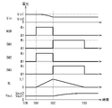
- FIG. 2 is a timing chart showing on/off of switches and a current IL flowing through an inductor forming the voltage conversion circuit shown in FIG.
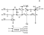
- FIG. 3 is a detailed circuit diagram of the switch circuit that constitutes the power supply circuit of the first embodiment, and is a circuit diagram showing the details of the switch indicated as HSW in FIG. 1 and its control circuit.
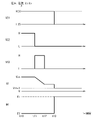
- FIG. 4 is a timing chart showing each voltage of the switch circuit shown in FIG. 3 and the time change of ON/OFF.
- FIG. 5 is a detailed circuit diagram of a switch circuit that constitutes the power supply circuit of the second embodiment, and is a circuit diagram showing the details of the switch indicated as HSW in FIG.
- FIG. 6 is a timing chart showing each voltage of the switch circuit shown in FIG. 5 and the time change of ON/OFF.
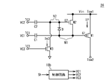
- FIG. 7 is a detailed circuit diagram of a switch circuit that constitutes the power supply circuit of the third embodiment, and is a circuit diagram showing the details of the switch indicated as HSW in FIG. 1 and its control circuit.
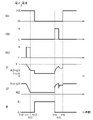
- FIG. 8 is a timing chart showing changes over time in each voltage, current and on/off of the switch circuit shown in FIG.
- FIG. 9 is a detailed circuit diagram of a switch circuit that constitutes the power supply circuit of the fourth embodiment, and is a circuit diagram showing the details of the switch indicated as HSW in FIG. 1 and its control circuit.
- FIG. 6 is a timing chart showing each voltage of the switch circuit shown in FIG. 5 and the time change of ON/OFF.
- FIG. 7 is a detailed circuit diagram of a switch circuit that constitutes the power supply circuit of the third embodiment, and is a circuit diagram showing the details of the switch indicated as HSW in FIG. 1 and its control circuit.
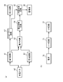
- FIG. 10(a) is a block diagram showing an embodiment of the power supply circuit of the present invention, in which the switch circuit of any one of the first to fourth embodiments and modifications thereof is used in the voltage conversion circuit 64.
- FIG. (b) is a block diagram showing a system of a sensor circuit in which the switch circuit of any one of Examples 1 to 4 and modifications thereof is used;
- FIG. 1 is a circuit diagram showing Example 1 of a power supply circuit using the switch circuit whose details are shown in FIG.
- the output current of the power generation element 10 is input to the input terminal Tin of the voltage conversion circuit 12 of FIG.
- the output current of the power generating element 10 is rectified by the rectifier circuit 11 and input to the input terminal Tin.
- the power generation element 10 is, for example, an energy harvesting element such as a vibration power generation element.
- the vibration power generating element is, for example, a piezoelectric element using a piezoelectric material or a MEMS element using MEMS (Micro Electro Mechanical Systems).
- Vibration power generation elements are provided, for example, on roads, bridges, or the like, and generate power from vibrations when pedestrians or vehicles pass by.
- the generated power is minute AC power, and changes with the state of vibration.
- the output voltage is relatively higher than the few volts typically required for electronic circuit operation.
- the rectifier circuit 11 causes the input to the input terminal Tin to be positive with respect to ground.
- Nodes N01 to N04 are provided between the input terminal Tin and the output terminal Tout of the voltage conversion circuit 12 .
- the voltage conversion circuit 12 of this embodiment steps down the relatively high voltage from the power generation element 10 and outputs it to the output terminal Tout.
- the switch HSW is a high side switch provided on the high voltage side (referred to as the high side) of the voltage conversion circuit 12 .
- a terminal Tsw1, which is one end of the switch HSW, is connected to the node N01, and a terminal Tsw2, which is the other end thereof, is connected to the node N02.
- One end of inductor L1 is connected to node N02, and the other end is connected to node N03.
- One end of the switch SW3 is connected to the node N03, and the other end is connected to the node N04.
- One end of the capacitor C01 on the primary side of the voltage conversion circuit 12 is connected to the node N01, and the other end is connected to the ground (reference potential).
- One end of the capacitor C02 on the secondary side of the voltage conversion circuit 12 is connected to the node N04, and the other end is connected to the ground.
- One end of the switch SW1 is connected to the node N02, and the other end is connected to the ground.
- One end of the switch SW2 is connected to the node N03, and the other end is connected to the ground.
- the control unit 14 outputs control signals Sh and S1 to S3 to the switches HSW and SW1 to SW3, respectively.
- the switches HSW and SW1 to SW3 are turned on or off based on the control signals Sh and S1 to S3, respectively.
- the control unit 14 generates the control signal Sh at regular intervals.
- the frequency is sufficiently higher than the frequency of the AC component contained in the electromotive force output from the power generation element 10 and the rectifier circuit 11 .
- the frequency of the control signal Sh is considered such that impedance matching is performed for efficiently transmitting the electromotive force output from the power generation element 10 and the rectifier circuit 11 to the voltage conversion circuit 12 .
- the control unit 14 may detect the voltages Vin and Vout and output the control signals Sh and S1 to S3 based on the voltages Vin and Vout.
- FIG. 2 is a timing chart showing the on/off of the switches and the current IL flowing through the inductor that constitute the voltage conversion circuit shown in FIG. FIG. 2 shows the value of the input voltage Vin, the ON and OFF states of each switch in FIG. 1, the current IL flowing through the inductor L1, and the value of the output voltage Vout.
- Time t00 in FIG. 2 is a timing during operation of the power supply circuit, and at that time, the current from the power generation element 10 is accumulated in the capacitor C01, and the voltage Vin is the voltage Vin1, which will be described later. A charge is also accumulated in the capacitor C02 by the voltage conversion operation, and the voltage Vout thereof is assumed to be the voltage Vout1.
- control unit 14 keeps switches HSW and SW1 to SW3 off.
- the control unit 14 After the electric charge accumulated in the capacitor C01 increases due to the current generated by the power generation element 10 and the voltage Vin exceeds a predetermined threshold voltage, the control unit 14 turns on the switches HSW and SW2 at time t01. , to keep the switches SW1 and SW3 off. As a result, a current IL begins to flow from the capacitor C01 to the ground via the node N01, the switch HSW, the inductor L1 and the switch SW2.
- the control unit 14 may detect the voltage Vin at the input terminal Tin and turn on the switches HSW and SW2 when the voltage Vin exceeds a predetermined threshold voltage, or may turn on the switches HSW and SW2 at predetermined intervals. good too. Between times t01 and t02, current IL gradually increases and voltage Vin gradually decreases as the charge of capacitor C01 is released. Magnetic field energy is stored in the inductor L1.
- control unit 14 turns off switches HSW and SW2 and turns on switches SW1 and SW3.
- the control unit 14 may detect the voltage Vin at the input terminal Tin, and turn off the switches HSW and SW2 and turn on the switches SW1 and SW3 when the voltage Vin reaches Vin2, or the switch HSW may be turned on at predetermined intervals. and SW2 may be turned off and the switches SW1 and SW3 may be turned on.
- the magnetic field energy stored in inductor L1 causes current IL to flow from ground through switch SW1, inductor L1 and switch SW3, and voltage Vout rises as capacitor C02 is charged.
- the control unit 14 turns off the switches SW1 and SW3 and keeps the switches HSW and SW2 off.
- the control unit 14 may detect the voltage Vout at the output terminal Tout, and turn off the switches SW1 and SW3 when the voltage Vout reaches a predetermined threshold voltage, or may turn off the switches SW1 and SW3 at predetermined intervals. good.
- current IL is 0, voltage Vin is voltage Vin2, and voltage Vout is voltage Vout2.
- Voltages Vout1 and Vout2 may be lower or higher than voltages Vin1 and Vin2.
- the voltages Vout1 and Vout2 can be set by appropriately setting the capacitance values of the capacitors C01 and C02 and the on/off timings of the switches HSW and SW1 to SW3.
- FIG. 3 is a detailed circuit diagram of the switch circuit that constitutes the power supply circuit of the first embodiment, and is a circuit diagram showing the details of the switch indicated as HSW in FIG. 1 and its control circuit.
- an FET whose channel has a P-type conductivity is referred to as a PFET
- an FET whose channel has an N-type conductivity is referred to as an NFET.
- ON/OFF of PFETM1 corresponds to ON/OFF of switch HSW. As shown in FIG.
- the source of PFETM1 (first FET) is connected to terminal Tsw1 (first terminal), the drain is connected to terminal Tsw2 (second terminal), and the gate is It is connected to the node N1 (first node).
- the capacitor C1 (first capacitor) has one end to which the control signal VC1 (first control signal) is input, and the other end connected to the node N1. That is, the gate is capacitively coupled to the control terminal TC1 (first control terminal).
- NFETM2 (second FET) has a source connected to node N1, a drain connected to terminal Tsw1, and a gate connected to control terminal TC2 to which control signal VC2 is input via capacitor C2 (second capacitor).
- the NFET M3 (third FET) has a source connected to the ground (reference potential), a drain connected to the node N1, and a gate connected to the control terminal TC3 to which the control signal VC3 is input.
- a control signal Sh output from the control section 14 in FIG. 1 is input to the control circuit 18a.
- the control circuit 18a controls the states of PFETM1, NFETM2 and NFETM3 by changing the levels of control signals VC1, VC2 and VC3 at timings based on control signal Sh.
- FIG. 4 is a timing chart showing each voltage and on/off time change of the switch circuit shown in FIG.
- the control circuit 18a sets the control signal VC1 to high level H (voltage X) and the control signal VC2 to high level H.
- the control signal VC3 is set to the low level. Since NFET M2 is on, voltage G1 is voltage Vin, and PFET M1 is off.
- the control unit 14 in FIG. 1 detects the voltage Vin of the input terminal Tin. At time t01 in FIG. Outputs an instruction to switch to the ON state.
- the control unit 14 may output a control signal Sh for switching the switch HSW from the OFF state to the ON state at a predetermined cycle.
- the control circuit 18a performs the operation of switching the PFET M1 from the off state to the on state between times t11 and t13.
- the control circuit 18a sets the control signal VC2 to low level L, sets the control signal VC3 to high level H, and maintains the control signal VC1 to high level H.
- NFET M2 is turned off and NFET M3 is turned on.
- a current Im3 flows from the node N1 to the ground.
- the voltage difference between the node N1 and the ground is in the saturation region of the NFET M3 (the region where the drain current is saturated)
- the current Im3 is substantially constant regardless of the voltage difference between the node N1 and the ground.
- the voltage G1 of the node N1 is gradually lowered by the current Im3 between times t11 and t12 in FIG.
- the control circuit 18a determines that a predetermined period of time has passed since time t11, at time t12, the control signal VC3 is set at low level L, the control signal VC1 is maintained at high level H, and the control signal VC2 is maintained at low level L. .
- NFET M3 is turned off.
- Voltage G1 is substantially constant between times t12 and t13.
- the voltage G1 is lower than the voltage Vin by the voltage difference X (the difference between the high level H and the low level L of the control signal VC1), and becomes the voltage Vin-X.
- PFET M1 is turned on. Since current IP flows through inductor L1 in FIG. 1, it gradually increases after time t12. Thus, NFET M2 is off while PFET M1 remains on.
- the node N1 becomes floating after the time t12, but if the interval between the times t12 and t13 is as short as several microseconds, for example, fluctuations in the voltage G1 pose no substantial problem. Since the voltage G1 is set to the voltage Vin-X, it is preferable that the control signal VC1 is set to the low level L after the timing when the control signal VC3 is set to the low level.
- the control circuit 18a charges or discharges the node N1 via the resistor (NFETM3) (between times t11 and t12) when turning the PFETM1 from the OFF state to the ON state. .
- the node N1 is set to floating (time t12), and after a predetermined time, the control signal VC1 is set to low level L (second level for turning on PFETM1) (time t13).
- PFET M1 is turned on.
- NFET M3 between times t11 and t12
- NFET M3 is off after time t13, so the potential of node N1 is floating. Therefore, no current flows between the terminal Tsw1 and the ground. Therefore, as in Patent Document 1, power consumption can be suppressed compared to the case where current continues to flow through the resistors R2 and R3 while the MOSFET (M1) (see FIG. 1 of Patent Document 1) is in the ON state.
- the control circuit 18a when turning PFET M1 from an off state to an on state, the control circuit 18a turns off NFET M2, disconnects node N1 from terminal Tsw1 (time t11), and then connects node N1 to the ground via NFET M3. (between times t11 and t12). After that, the control circuit 18a disconnects the node N1 from the ground (time t12) and supplies a low level L to the control terminal TC1 (time t13).
- the voltage G1 can be stably set to the voltage Vin-X due to the drop in the voltage G1 due to the capacitive coupling of the capacitor C1 and the drop in the voltage G1 due to the current Im3 of the NFET M3. Therefore, the PFET M1 can be stably turned on from the off state. Thereby, when the voltage conversion circuit 12 should operate, the voltage conversion circuit 12 operates stably, and the conversion efficiency can be improved.
- a PFET may be used as the third FET corresponding to NFETM3.
- the voltage G1-X is used as the control signal VC3 for turning on the first switch. Since the voltage G1 fluctuates as shown in the graph of FIG. 4, a generating circuit that follows the fluctuation of the voltage G1 and generates the control signal VC3 may be provided.
- the control signal VC3 may be set at a constant voltage (high level H) with respect to the ground to turn on the third FET, and the control signal VC3 is generated. is easy.
- the first switch can be stably turned on at a predetermined timing.
- an NFET is used for the first switch, compared to the case of using a PFET, the generation circuit described above is not required, and the power consumption of the generation circuit does not increase the power consumption of the entire power supply circuit.
- the control signal VC3 is at the high level H (first level)
- the control signal is a voltage value set so that a saturation current flows between the source and the drain of the NFETM3.
- the control circuit 18a is configured to output VC3.
- the current Im3 can be kept constant without depending on the voltage difference between the node N1 and the ground.
- the drop in voltage G1 at time t12 from time t11 can be made substantially constant, regardless of the voltage value of voltage Vin. Therefore, the voltage G1 at time t13 can be approximately the voltage Vin-X, regardless of the voltage value of the voltage Vin. Therefore, the PFET M1 can be stably turned on from the off state. Thereby, the voltage conversion circuit 12 operates when the voltage conversion circuit 12 should operate, and the conversion efficiency can be improved.
- a PFET may be used as the second FET corresponding to NFETM2.
- the control signal VC2 may be set to the voltage G1 or a constant voltage (high level H) with respect to the ground when turning on the second FET.
- the second FET can be stably turned on at a predetermined timing.
- Example 1 the first terminal Tsw1 connected to the power generation element 10, the second terminal Tsw2, the source connected to the first terminal Tsw1, the drain connected to the second terminal Tsw2, the first A first FET having a gate connected to the first node N1 capacitively coupled to the control terminal TC2 was taken as PFET M1 in FIG.
- the first FETM1 When the first FETM1 maintains either the OFF state or the ON state, the first level at which the first FETM1 is in one of the states is supplied to the first control terminal TC1, and the first FETM1 is switched to one of the states. , the first node N1 is charged or discharged through a resistor, then the first node N1 is made floating, and the first FET M1 is connected to the first control terminal TC1.
- the control circuit 18a for supplying the second level to set the state was composed of NFETM2, NFETM3, and the control circuit 18a for supplying VC1, VC2, VC3.
- the control signal Sh has a constant cycle, and its frequency is sufficiently higher than the frequency of the AC component contained in the electromotive force output from the power generation element 10 and the rectifier circuit 11.
- the frequency of the control signal Sh increases, the power consumption of the FETs M1 to M3 increases. Therefore, in order to efficiently transmit the power generated in the power generating element 10 to the capacitor C02 in the subsequent stage, it is preferable that the frequency of the control signal Sh is low.
- the control signal Sh is generated in a constant cycle, but the voltage of the secondary capacitor C02 (node N04) is required to drive the load instead of the constant cycle.
- the control signal Sh may be generated by detecting that a predetermined voltage has been reached by a comparator.
- the control signal Sh may be generated by detecting that the voltage of the primary capacitor C01 (node N01) has reached a predetermined voltage with a comparator.
- the control signal VC3 may become high level H after the switch SW5 is turned off.
- control terminal TC2 and the gate of NFETM2 are capacitively coupled.
- the control circuit 18a switches the control signal VC2 from the low level L to the high level H, and the voltage G2 of the gate of the NFET M2 becomes the high level H.
- NFET M2 is turned on.
- voltage G2 is not stable.
- the voltage G2 is stable during the period in which the gate of NFET M2 is floating, depending on the period in which the control signal VC1 is set to high level and low level or circuit constants such as the saturation current value between the source and drain of NFET M3. It is conceivable that they may not. In this case, the operation of the switch HSW (PFETM1) may not be stable, and the power supply circuit as a whole may not exhibit the desired performance.
- Embodiment 2 will explain a switch circuit that exhibits desired performance as a power supply circuit even in such a case.
- FIG. 5 is a detailed circuit diagram of the switch circuit that constitutes the power supply circuit of the second embodiment, and is a circuit diagram showing the details of the switch indicated as HSW in FIG. 1 and its control circuit.
- the control signal VC2 is input to one end of the capacitor C2 (second capacitor), and the other end is connected to the node N2 (second node).
- Diode D rectifying element
- Diode D has an anode connected to node N1 and a cathode connected to node N2 between NFET M2 and capacitor C2.
- the direction from node N1 to N2 is the forward direction.
- the drain of NFET M3 is connected through node N2 and diode D to node N1.
- NFET M2 (second FET) has a source connected to node N1, a drain connected to terminal Tsw1, and a gate connected to node N2 capacitively coupled to control terminal TC2 (second control terminal).
- Other configurations of the power supply circuit are the same as those of the first embodiment, and description thereof is omitted.
- FIG. 6 is a timing chart showing the time change of each voltage and on/off of the switch circuit shown in FIG.
- the control circuit 18b sets the control signal VC1 to high level H (voltage X), the control signal VC2 to low level L, and the control signal VC3 is set to low level L.
- the voltage G1 is set to the voltage Vin in the same state as after time t16.
- Voltage G2 becomes voltage Vin- ⁇ V.
- ⁇ V is the forward voltage drop of diode D;
- control circuit 18b When the control signal Sh instructs switching of the switch HSW from the OFF state to the ON state, the control circuit 18b performs an operation of switching the PFET M1 from the OFF state to the ON state between times t11 and t13. At time t11, control circuit 18b raises control signal VC3 to high level H, while maintaining control signals VC1 and VC2 at high level H and low level L, respectively. As a result, NFET M3 is turned on, and current Im3 flows from nodes N2 and N1 to the ground. Between times t11 and t12, voltage G2 drops due to current Im3, and current flows from node N1 to node N2 via diode D, causing voltage G1 to drop.
- the control circuit 18b sets the control signal VC3 to low level L, and maintains the control signals VC1 and VC2 at high level H and low level L, respectively.
- NFET M3 is turned off.
- Voltage G2 becomes VG2.
- the voltage G1 becomes VG2+ ⁇ V.
- Voltage G1 is substantially constant between times t12 and t13.
- the control circuit 18b sets the control signal VC1 to the low level and maintains the control signals VC2 and VC3 at the low level. As a result, the voltage G1 becomes the voltage Vin-X.
- PFET M1 is turned on and current IP flows.
- the control circuit 18b sets the control signals VC1 to VC3 to the low level between times t13 and t14 when the switch HSW remains on.
- the control unit 14 in FIG. 1 detects the voltage Vin of the input terminal Tin. At time t02 in FIG. Outputs an instruction to switch to the OFF state.
- the control unit 14 may output a control signal Sh for switching the switch HSW from the ON state to the OFF state at a predetermined cycle.
- the control circuit 18b performs the operation of switching the PFET M1 from the on state to the off state between times t14 and t16.
- the control circuit 18b sets the control signal VC2 to high level H, and maintains the control signals VC1 and VC3 at low level L.
- the control circuit 18b sets the control signal VC2 to low level L, and maintains the control signals VC1 and VC3 at low level L.
- Voltage G2 becomes low.
- voltage G2 becomes lower than voltage G1- ⁇ V, current flows through diode D from node N1 to node N2. As a result, the voltage G1 drops slightly, the voltage G2 rises slightly, and the voltages G1 and G2 become balanced voltages.
- the control circuit 18b sets the control signal VC1 to high level H, and maintains the control signals VC2 and VC3 at low level L.
- the voltage G1 of the node N1 capacitively coupled with the control terminal TC1 rises.
- Voltage G2 becomes voltage Vin- ⁇ V. Since voltage G2 is stable, voltage G1 is stable and PFET M1 is stable in the off state.
- the control circuit 18b in addition to turning PFET M1 from an off state to an on state, connects the node N2 to a resistance (that is, a voltage between the source and drain of NFET M2) when turning PFET M1 from an on state to an off state. (between time t14 and time t15). After that, the control circuit 18b makes the node N2 floating (time t15) and supplies a low level L to the control terminal TC2 (time t16).
- the control circuit 18b sets the control terminal TC1 to the first level (PFETM1 is set to either the off state or the on state).
- Control circuit 18b charges or discharges node N1 via a resistor (between times t11 and t12 and between t14 and t15). After that, the control circuit 18b makes the node N1 floating (at times t12 and t15), and supplies a potential of the second level (the level at which the PFET M1 is turned off or on) to the control terminal TC1 (at times t13 and t15). t16).
- the PFET M1 (switch element) is an electric field control type switch element that can be switched between an ON state and an OFF state according to the potential (voltage G1) of the gate, which is the control terminal.
- the gate of the control circuit 18a is supplied with a potential of the first level that causes the PFET M1 to be in either the off state or the on state.
- the gate is charged or discharged through a resistor and then floated to a second level potential for bringing PFET M1 to the other state. supply.
- the node N1 is floating, so power consumption can be suppressed.
- a capacitor C2, a diode D and an NFET M2 are provided as a maintenance circuit for maintaining the voltage G1 within a predetermined range.
- PFET M1 when PFET M1 is turned on from the off state, when NFET M3 is turned on from time t11 to t12, a current flows from node N1 to the ground through diode D and node N2, and voltages G1 and G2 rise. descend. Therefore, the NFET M2 can be switched from the ON state to the OFF state, and the PFET M1 can be switched from the OFF state to the ON state, without depending on the voltage value of the voltage Vin.
- the control circuit 18b supplies a low level L (second level) to the control terminal TC1 and a low level L (NFET M3) to the control terminal TC2 when the PFET M1 maintains the ON state, such as times t13 and t14.
- a third level potential for turning off is supplied.
- the control circuit 18b supplies a potential of high level H (fourth level for turning on the NFET M3) to the control terminal TC2 when turning the PFET M1 from the ON state to the OFF state.
- the NFET M2 When the control signal VC2 becomes high level H and the voltage G2 rises, the NFET M2 is turned on and the voltages G1 and G2 rise. After that, by setting the control signal VC1 to the high level H, the voltage G1 can be further increased. As a result, the voltage G1 can be stabilized at the voltage Vin, and the voltage G2 can be stabilized at the voltage Vin+.DELTA.V.
- the control circuit 18b supplies a low level L (third level) to the control terminal TC2 at time t15 when turning the PFETM1 from an ON state to an OFF state, and then, at time t16 after a predetermined time has passed, the control terminal TC1 is set at a high level.
- level H first level
- the high level H second level
- the PFET M1 can be stably turned off. Therefore, it is possible to suppress an unintended current from flowing through the voltage conversion circuit 12, and the conversion efficiency in the voltage conversion circuit 12 can be improved.
- the high level H of the control signal VC2 is 2V, for example, and the high level H of the control signal VC1 is 1V, for example.
- the high level H of the control signal VC2 is preferably higher than the high level H of the control signal VC1.
- the voltage G2 can be further increased between times t14 and t15.
- the PFET M1 can be turned off more stably, so that the conversion efficiency in the voltage conversion circuit 12 can be improved.
- FIG. 7 is a detailed circuit diagram of the switch circuit that constitutes the power supply circuit of the third embodiment, and is a circuit diagram showing the details of the switch indicated as HSW in FIG. 1 and its control circuit.
- the control signal Sh has a constant cycle, and its frequency is sufficiently higher than the frequency of the AC component contained in the electromotive force output from the power generation element 10 and the rectifier circuit 11 .
- the power consumption of the FETM1 to M3 increases in proportion to the increase in the frequency of the control signal Sh. Therefore, in order to efficiently transmit the power generated in the power generation element 10 to the capacitor C02 in the subsequent stage, it is preferable that the frequency of the control signal Sh is low.
- the electromotive force of the power generation element 10 is large, and the switch HSW is in the OFF state at intervals between the high level and the low level of the control signal Sh, that is, the voltage at which no current flows between the source and the drain of the FET M1 at the node N1.
- Sh the voltage at which no current flows between the source and the drain of the FET M1 at the node N1.
- the voltage Vin rises significantly (e.g., 0.3 V or more) and becomes a voltage that causes a minute current to flow between the source and the drain of FETM1.
- the charge in the capacitor C01 does not contribute to the voltage conversion by the amount of , and there is a fear that the voltage conversion efficiency is lowered.
- the third embodiment has a switch circuit 27, a judgment circuit 15, a comparator 16, an NFET M4 and a capacitor C3 as shown in FIG.
- the reset signal Vr when the voltage Vin fluctuates to Vref or more, it outputs the reset signal Vr to the control circuit 18c.
- This reset signal Vr resets the gate potential of the PFET M1 to the same potential as the voltage Vin, like the control signal Sh of the second embodiment.
- one end of capacitor C3 is connected to node N4 between the source of PFET M1 and terminal Tsw1, and the other end is connected to node N3 (third node). That is, the node N3 is capacitively coupled to the terminal Tsw1.
- NFET M4 has a source connected to ground, a drain connected to node N3, and a gate connected to control terminal TC4 to which control signal VC4 is input.
- the comparator 16 has a positive input terminal connected to the node N3, a negative input terminal to which the reference voltage Vref is input, and an output terminal to output the reset signal Vr.
- the comparator 16 outputs a high level H as the reset signal Vr when the voltage Vm of the node N3 is equal to or higher than the reference voltage Vref, and outputs a low level L as the reset signal Vr when the voltage Vm is lower than the reference voltage Vref.
- the reference voltage Vref is, for example, 0.3V.
- control signal Sh output by the control unit 14 and the reset signal Vr output by the comparator 16 are input to the control circuit 18c.
- the control circuit 18c outputs control signals VC1 to VC4 based on the control signal Sh and the reset signal Vr.
- Other configurations are the same as those of the second embodiment, and description thereof is omitted.
- FIG. 8 is a timing chart showing changes over time in each voltage, current, and on/off of the switch circuit shown in FIG.
- the input current Iin input from the rectifier circuit 11 to the terminal Tsw1 varies depending on the power generation amount of the power generating element 10.
- Iin1 is very small until time t20, and after time t20 Iin2.
- the current Iin1 hardly affects the voltage Vin or the like in this timing chart. Therefore, voltage Vin from time t10 to t13 and from time t14 to t20 is substantially constant. Between times t13 and t14, charge moves from capacitor C1 to capacitor C2, causing voltage Vin to drop slightly.
- control signals VC1 to VC3 are the same as those in FIG. 6 of the second embodiment, and description thereof is omitted.
- NFET M4 is turned on at a predetermined timing, so voltage Vm at time t10 is zero.
- the control signal VC4 is at low level L between times t10 and t16, and the reset signal Vr remains at low level L.
- the control circuit 18c detects the voltage Vin of the terminal Tsw1.
- the voltage Vin exceeds the voltage Vin0+Vref
- the voltage Vm exceeds the reference voltage Vref
- the comparator 16 outputs a high level H as the reset signal Vr. do.
- the control circuit 18c sets the control signal VC1 to low level L and sets the control signal VC2 to high level H, while maintaining the control signals VC3 and VC4 at low level L.
- the voltage G1 at the node N1 capacitively coupled to the control terminal TC1 drops.
- Voltage G2 at node N2 capacitively coupled to control terminal TC2 rises. Note that the timing at which the control signal VC1 is set at low level L and the timing at which the control signal VC2 is set at high level H may be slightly different as long as the above operation is possible.
- control circuit 18c sets the control signal VC2 to the low level L and maintains the control signals VC1, VC3 and VC4 at the low level L.
- Voltage G2 at node N2 capacitively coupled to control terminal TC2 drops.
- control circuit 18c sets control signals VC1 and VC4 to high level H, and maintains control signals VC2 and VC3 at low level L.
- the voltage G1 becomes Vin0+Vref, which is the voltage of the voltage Vin, in the same way that the voltage G1 becomes the voltage Vin0 of the voltage Vin.
- NFET M4 is turned on, and voltage Vm of node N3 becomes 0V.
- the timing at which the control signal VC1 is set to the high level H and the timing at which the control signal VC4 is set to the high level H may be slightly different as long as the voltage Vm of the node N3 can be appropriately set to 0V.
- the control circuit 18c sets the control signal VC4 to the low level L, maintains the control signal VC1 at the high level H, and maintains the control signals VC2 and VC3 at the low level L.
- the comparator 16 compares the voltage Vm of the node N3 with the reference voltage Vref, and outputs the comparison result to the control circuit 18c.
- the determination circuit 15 can determine whether or not the voltage Vin has changed by a constant voltage corresponding to the reference voltage Vref in the higher direction (farther from the reference potential 0 V) than the voltage Vin0.
- the determination circuit 15 determines that the voltage Vin is higher than the voltage Vin0 (the voltage when the PFETM1 was previously switched from the ON state to the OFF state) (further from the reference potential 0V). method) is determined to have changed by a constant voltage (Vref).
- Vref constant voltage
- the voltage G1 of the gate of the PFET M1 can be set to the voltage Vin again. Therefore, it is possible to suppress a minute current from flowing between the source and the drain of the FETM1 during the period when the voltage Vin rises from the voltage Vin0 and the FETM1 is controlled to be in the OFF state, and the charge of the primary capacitor flows out. can be suppressed. Thereby, it is possible to prevent the conversion efficiency of the voltage conversion circuit 12 from decreasing.
- control signal Sh has a constant cycle, and as described above, it is desirable that the frequency is low. Actions therefore take precedence.
- Example 4 is an example in which the input voltage Vin from the power generation element 10 is lower than the ground potential.
- FIG. 9 is a detailed circuit diagram of a switch circuit that constitutes the power supply circuit of the fourth embodiment, and is a circuit diagram showing the details of the switch indicated as HSW in FIG. 1 and its control circuit.
- NFETM1a, PFETM2a, M3a and M4a are used in place of PFETM1, NFETM2, M3 and M4 of FIG. 7 of Example 3, respectively.
- Diode D has its cathode connected to node N1 and its anode connected to node N2, and the direction from node N2 to N1 is the forward direction.
- the negative input terminal of the comparator 16a is connected to the node N3, and the reference voltage Vref is input to the positive input terminal.
- the control circuit is 18d. The rest of the configuration is the same as that of FIG. 7 of the third embodiment, and description thereof is omitted.
- the high level H and low level L of the control signals VC1 to VC4 are opposite to those in FIG. Voltage X, voltage Vin0 and reference voltage Vref are negative.
- the first FET when the input voltage Vin is higher than the ground (reference potential), the first FET is PFET M1, and the second and third FETs are NFETs M2 and M3, respectively.
- the first level and fourth level are high level H, and the second level and third level are low level L.
- FIG. when the input voltage Vin is lower than ground (reference potential), the first FET is NFET M1a and the second and third FETs are PFETs M2a and M3a, respectively.
- the first and fourth levels are low level L, and the second and third levels are high level H.
- the second and third FETs are of the type of NFET and PFET opposite in channel conductivity type to the first FET.
- the PFET is in the off state when the gate voltage (voltage of gate to source) is 0V, and is in the on state when the gate voltage is lower than the negative threshold voltage.
- the NFET is off when the gate voltage is 0V and is on when the gate voltage is above the positive threshold voltage.
- PFET and NFET are MOS (Metal Oxide Semiconductor) FETs using silicon, for example.
- a diode D is, for example, a diode in which an FET is diode-connected.
- the switch element may be a field effect switch element in which the potential applied to the control terminal switches between the ON state and the OFF state of the conductive channel according to the electric field formed in the conductive channel.
- it may be a bipolar transistor or IGBT (Insulated Gate Bipolar Transistor) combined with an FET.
- the high level and low level of the control signals VC1 to VC4 may be the same control signal, as long as the high level is higher than the low level. can be different from each other.
- the switches of Embodiments 1 to 4 in the voltage conversion circuit 12 of FIG. 1 can be stably controlled.
- the power supply circuit may be a step-down voltage conversion circuit, a step-up voltage conversion circuit, or an inversion voltage conversion circuit.
- the power supply circuit may be a power conversion circuit or the like that converts alternating current to direct current.
- FIG. 10(a) is a block diagram showing an embodiment of the power supply circuit of the present invention, in which the voltage conversion circuit 64 uses the switch circuit of any one of Embodiments 1 to 4 and modifications thereof.
- the system includes a power generation element 60 , rectifier circuits 61 and 62 , matching circuit 63 , voltage conversion circuit 64 , charge management circuit 65 , capacitor 66 , cold start circuit 67 and booster circuit 68 . ing.
- the power generation element 60 is, for example, the power generation element 10 in FIG. 1, and generates AC power of minute current.
- the rectifier circuit 61 is, for example, a diode bridge, and the rectifier circuit 62 is, for example, a synchronous rectifier circuit.
- Matching circuit 63 matches the output impedance of rectifying circuits 61 and 62 and the input impedance of voltage converting circuit 64 .
- the voltage conversion circuit 64 is, for example, the voltage conversion circuit 12 in FIG. 1 and is a DC-DC converter.
- the charge management circuit 65 charges the appropriate capacitor 66 out of the plurality of capacitors 66 .
- the capacitor 66 is, for example, a capacitor.
- a charge management circuit 65 monitors the voltage across a plurality of capacitors and charges the appropriate capacitor with generated power.
- the cold start circuit 67 charges the capacitor 66 with the output current of the rectifier circuit 61 when the capacitor 66 is hardly charged.
- the booster circuit 68 is, for example, a charge pump, and generates a voltage used for the rectifier circuit 62, the voltage conversion circuit 64, and the like.
- the rectifier circuit 61 rectifies the minute power.
- the rectifier circuit 61 can perform rectification without an external power source like a diode bridge.
- the current rectified by the rectifier circuit 61 reaches the charge management circuit 65 via the cold start circuit 67 and is stored in the capacitor 66 .
- boost circuit 68 boosts the voltage of capacitor 66 to the voltage used by rectifier circuit 62 and voltage conversion circuit 64 .
- the voltage of the capacitor 66 is, for example, 1V
- the output voltage of the booster circuit 68 is, for example, 2V. If the rectifying circuit 62 and the voltage converting circuit 64 operate using the voltage of the capacitor 66, the booster circuit 68 may be omitted.
- the matching circuit 63 increases the input power when the amount of power generated by the power generation element 60 is large and the generated current is large, and increases the input power when the amount of power generated by the power generation element 60 is small and the generated current is small. Thereby, the output impedance of the power generation element 60 and the input impedance of the rectifier circuits 61 and 62 are matched.
- the matching circuit 63 switches between the rectifier circuits 61 and 62 according to the input voltage. For example, if the rectifier circuits 61 and 62 are a diode bridge and a synchronous rectifier circuit, respectively, the loss due to the on voltage of the diodes increases when the input voltage is 1 V or less. Therefore, the rectifier circuit 62 is used. When the input voltage is 1V or more, the rectifier circuit 61 is used.
- the voltage conversion circuit 64 converts the input voltage set by the matching circuit 63 into a voltage that charges the capacitor 66 .
- the voltage of capacitor 66 is, for example, 1V or 3.3V.
- a charge management circuit 65 monitors the voltages of a plurality of capacitors 66 and charges appropriate capacitors 66 with generated power.
- the input voltage of the voltage conversion circuit 64 changes.
- the switch HSW (see FIG. 1), which is the high-side switch of the voltage conversion circuit 64, may not operate stably, and the conversion efficiency of the voltage conversion circuit 64 may decrease.
- the switch circuit of the first to fourth embodiments as the switch HSW of the voltage conversion circuit, the switch HSW can be stably controlled, and the reduction in the conversion efficiency of the voltage conversion circuit 64 can be suppressed.
- FIG. 10(b) is a block diagram showing a sensor circuit system using the switch circuit of any one of Examples 1 to 4 and its modifications.
- the switch element of the switch circuit 71 of Examples 1 to 4 turns on and off power supply from the power source 70 to the sensor circuit 72 .
- the switch elements of the switch circuits of the first to fourth embodiments are not limited to the elements that turn on and off the electromotive force supplied from the power generation element.
- the switch circuits of Embodiments 1 to 4 may be used in circuits other than power supply circuits, such as IoT (Internet of Things) devices with low power consumption or edge devices.
- IoT Internet of Things
Landscapes
- Engineering & Computer Science (AREA)
- Power Engineering (AREA)
- Dc-Dc Converters (AREA)
Abstract
Description
12 電圧変換回路
14 制御部
16 比較器
18a~18d 制御回路
Claims (19)
- 制御端子の電位に応じてオン状態とオフ状態が切り替えられる電界効果型スイッチ素子と、
前記スイッチ素子のオン状態およびオフ状態のいずれか一方を維持させる際に、前記制御端子に前記スイッチ素子を前記いずれか一方の状態にさせる第1レベルの電位を供給し、前記スイッチ素子を前記いずれか一方の状態からオン状態およびオフ状態の他方の状態にさせる際に、前記制御端子を、抵抗を介し充電または放電した後フローティングとし、前記スイッチ素子を前記他方の状態にさせる第2レベルの電位を供給する制御回路と、
を備えるスイッチ回路。 - 前記制御回路は前記制御端子に前記第1レベルの電位を供給する際に、前記制御端子をフローティングとする請求項1に記載のスイッチ回路。
- 前記スイッチ素子は発電素子から供給される起電力のオンオフを行う素子である請求項1または2に記載のスイッチ回路。
- 前記スイッチ素子はセンサ回路への電力供給のオンオフを行う素子である請求項1から3のいずれか一項に記載のスイッチ回路。
- 前記制御端子の電位を所定の範囲内に維持する維持回路を有する請求項1から4のいずれか一項に記載のスイッチ回路。
- 前記維持回路は前記制御端子に接続されたダイオードを含む請求項5に記載のスイッチ回路。
- 前記スイッチ素子は、第1端子に接続されたソースと、第2端子に接続されたドレインと、第1制御端子に容量結合する第1ノードに接続されたゲートと、を有する第1FETである請求項1から6のいずれか一項に記載のスイッチ回路。
- 前記第1ノードに接続されたソースと、前記第1端子に接続されたドレインと、ゲートと、を有する第2FETを備え、
前記いずれか一方の状態はオフ状態であり、
前記制御回路は、前記第1FETをオフ状態からオン状態とするときに、前記第2FETのソースとドレインとの間をオフ状態とし前記第1ノードを前記抵抗を介し基準電位に接続し、その後前記第1ノードを前記第1端子および前記基準電位から切断しかつ前記第1制御端子に前記第2レベルの電位を供給する請求項7に記載のスイッチ回路。 - 前記基準電位に接続されたソースと、前記第1ノードに接続されたドレインと、ゲートと、を有する第3FETを備え、
前記抵抗は前記第3FETのソースとドレインとの間の抵抗であり、前記第1ノードを前記第2FETを介し前記基準電位に接続するとき前記第3FETに飽和電流が流れる請求項8に記載のスイッチ回路。 - 前記第1ノードから第2制御端子に容量結合する第2ノードの方向が順方向となる整流素子を備え、
前記第2FETはNタイプであり、前記第2FETのゲートは前記第2ノードに接続され、
前記第1FETはPタイプであり、
前記第1ノードは、前記整流素子、前記第2ノードおよび前記抵抗を介し前記基準電位に接続される請求項8または9に記載のスイッチ回路。 - 第2制御端子に容量結合する第2ノードから前記第1ノードの方向が順方向となる整流素子を備え、
前記第2FETはPタイプであり、前記第2制御端子に容量結合する第2ノードに接続され、
前記第1FETはNタイプであり、
前記第1ノードは、前記整流素子、前記第2ノードおよび前記抵抗を介し前記基準電位に接続される請求項8または9に記載のスイッチ回路。 - 前記制御回路は、前記第1FETがオン状態を維持するときに、前記第1制御端子に前記第2レベルの電位を供給し、かつ前記第2制御端子に前記第2FETをオフ状態とさせる第3レベルの電位を供給し、前記第1FETをオン状態からオフ状態とさせるときに、前記第2制御端子に前記第2FETをオン状態とさせる第4レベルの電位を供給し、その後、前記第1制御端子に前記第1レベルの電位を供給しかつ前記第2制御端子に前記第3レベルの電位を供給する請求項10または11に記載のスイッチ回路。
- 前記制御回路は、前記第1FETをオン状態からオフ状態とするときに、前記第2制御端子に前記第3レベルの電位を供給した後、前記第1制御端子に前記第1レベルの電位を供給する請求項12に記載のスイッチ回路。
- 前記第1FETがオフ状態を維持するときに、前記第1端子に入力する入力電圧が前記第1FETがオン状態からオフ状態に前回切り替わったときの入力電圧から一定電圧変化したことを判定する判定回路を備え、
前記制御回路は、前記入力電圧が一定電圧変化したと判定したとき、前記第1制御端子に前記第2レベルを供給しかつ前記第2制御端子に前記第4レベルを供給し、その後、前記第1制御端子に前記第1レベルを供給しかつ前記第2制御端子に前記第3レベルを供給する請求項12または13に記載のスイッチ回路。 - 前記判定回路は、
前記第1端子に容量結合された第3ノードの電圧と一定電圧とを比較し、比較結果を前記制御回路に出力する比較器を備える請求項14に記載のスイッチ回路。 - 前記第1端子に入力する入力電圧は前記基準電位より高く、前記第1FETはPFETである請求項8から15のいずれか一項に記載のスイッチ回路。
- 前記第1端子に入力する入力電圧は前記基準電位より低く、前記第1FETはNFETである請求項8から15のいずれか一項に記載のスイッチ回路。
- 前記発電素子は振動発電素子である請求項3記載のスイッチ回路。
- 請求項1から18のいずれか一項に記載のスイッチ回路を備える電源回路。
Priority Applications (3)
| Application Number | Priority Date | Filing Date | Title |
|---|---|---|---|
| CN202280023944.3A CN117083786B (zh) | 2021-03-25 | 2022-03-17 | 开关电路和电源电路 |
| JP2023509100A JP7879610B2 (ja) | 2021-03-25 | 2022-03-17 | スイッチ回路および電源回路 |
| US18/369,461 US12328115B2 (en) | 2021-03-25 | 2023-09-18 | Switching circuit and power supply circuit |
Applications Claiming Priority (2)
| Application Number | Priority Date | Filing Date | Title |
|---|---|---|---|
| JP2021-051423 | 2021-03-25 | ||
| JP2021051423 | 2021-03-25 |
Related Child Applications (1)
| Application Number | Title | Priority Date | Filing Date |
|---|---|---|---|
| US18/369,461 Continuation US12328115B2 (en) | 2021-03-25 | 2023-09-18 | Switching circuit and power supply circuit |
Publications (1)
| Publication Number | Publication Date |
|---|---|
| WO2022202609A1 true WO2022202609A1 (ja) | 2022-09-29 |
Family
ID=83395792
Family Applications (1)
| Application Number | Title | Priority Date | Filing Date |
|---|---|---|---|
| PCT/JP2022/012286 Ceased WO2022202609A1 (ja) | 2021-03-25 | 2022-03-17 | スイッチ回路および電源回路 |
Country Status (4)
| Country | Link |
|---|---|
| US (1) | US12328115B2 (ja) |
| JP (1) | JP7879610B2 (ja) |
| CN (1) | CN117083786B (ja) |
| WO (1) | WO2022202609A1 (ja) |
Citations (2)
| Publication number | Priority date | Publication date | Assignee | Title |
|---|---|---|---|---|
| WO2000008759A1 (fr) * | 1998-08-03 | 2000-02-17 | Hitachi, Ltd. | Circuit integre a mos |
| JP2002010631A (ja) * | 2000-06-22 | 2002-01-11 | Texas Instr Japan Ltd | 駆動回路 |
Family Cites Families (6)
| Publication number | Priority date | Publication date | Assignee | Title |
|---|---|---|---|---|
| JP4671275B2 (ja) * | 2005-01-26 | 2011-04-13 | ルネサスエレクトロニクス株式会社 | 電源制御装置、電源用電子部品及び電源装置 |
| JP2011030327A (ja) * | 2009-07-23 | 2011-02-10 | Asahi Kasei Electronics Co Ltd | 電源回路装置 |
| CN101753000A (zh) * | 2009-12-17 | 2010-06-23 | 东南大学 | 栅极浮置及电平转换的功率mos管栅极驱动电路及方法 |
| JP6002497B2 (ja) | 2012-08-01 | 2016-10-05 | 鳥取コスモサイエンス株式会社 | 電源回路 |
| JP6451429B2 (ja) * | 2015-03-16 | 2019-01-16 | 株式会社デンソー | スイッチング素子の駆動装置 |
| WO2020175209A1 (ja) | 2019-02-28 | 2020-09-03 | 国立研究開発法人科学技術振興機構 | スパイク生成回路、情報処理回路、電力変換回路、検出器および電子回路 |
-
2022
- 2022-03-17 JP JP2023509100A patent/JP7879610B2/ja active Active
- 2022-03-17 WO PCT/JP2022/012286 patent/WO2022202609A1/ja not_active Ceased
- 2022-03-17 CN CN202280023944.3A patent/CN117083786B/zh active Active
-
2023
- 2023-09-18 US US18/369,461 patent/US12328115B2/en active Active
Patent Citations (2)
| Publication number | Priority date | Publication date | Assignee | Title |
|---|---|---|---|---|
| WO2000008759A1 (fr) * | 1998-08-03 | 2000-02-17 | Hitachi, Ltd. | Circuit integre a mos |
| JP2002010631A (ja) * | 2000-06-22 | 2002-01-11 | Texas Instr Japan Ltd | 駆動回路 |
Also Published As
| Publication number | Publication date |
|---|---|
| US20240007102A1 (en) | 2024-01-04 |
| CN117083786A (zh) | 2023-11-17 |
| CN117083786B (zh) | 2026-08-04 |
| JPWO2022202609A1 (ja) | 2022-09-29 |
| JP7879610B2 (ja) | 2026-06-24 |
| US12328115B2 (en) | 2025-06-10 |
Similar Documents
| Publication | Publication Date | Title |
|---|---|---|
| CN112542937B (zh) | 用于被配置为驱动高侧开关晶体管的驱动电路的浮动电源 | |
| JP5169170B2 (ja) | 降圧型スイッチングレギュレータ | |
| CN100448144C (zh) | 电源电路 | |
| US7368900B2 (en) | Constant voltage circuit and constant current source, amplifier, and power supply circuit using the same | |
| US12401287B2 (en) | Systems and methods for providing power to pulse-width-modulation controllers of power converters during normal operation | |
| US8018214B2 (en) | Regulator with soft-start using current source | |
| US8508196B2 (en) | Switching regulator | |
| JP6018749B2 (ja) | チャージポンプシステムを制御するための回路および方法 | |
| US20250055380A1 (en) | Systems and methods for controlling synchronous rectification with variable voltage regulation | |
| US20250070645A1 (en) | Gate drive circuit, power good circuit, overcurrent detection circuit, oscillation prevention circuit, switching control circuit and switching power supply device | |
| US7274577B2 (en) | Electronic instrument having booster circuit | |
| CN107735932A (zh) | 具有自适应死区时间的升压调节器 | |
| US20100164456A1 (en) | Control circuit and control method for switching regulator | |
| EP1879284B1 (en) | DC-DC converter and power supply apparatus | |
| JP7332831B1 (ja) | 制御回路及び整流回路 | |
| JP2008079448A (ja) | 昇圧電源装置 | |
| JP2018121377A (ja) | スイッチング電源装置 | |
| US12308745B2 (en) | Switching circuit and power supply circuit | |
| JP2018196201A (ja) | Dc/dcコンバータ | |
| JP2011166851A (ja) | スイッチング制御回路およびスイッチング電源回路 | |
| CN117083786A (zh) | 开关电路和电源电路 | |
| JP5593104B2 (ja) | リップルコンバータ | |
| JP7216846B1 (ja) | 電力変換装置の制御回路 | |
| CN109804563B (zh) | 一种整流电路及整流器 | |
| CN112311226B (zh) | 升压电路 |
Legal Events
| Date | Code | Title | Description |
|---|---|---|---|
| 121 | Ep: the epo has been informed by wipo that ep was designated in this application |
Ref document number: 22775397 Country of ref document: EP Kind code of ref document: A1 |
|
| WWE | Wipo information: entry into national phase |
Ref document number: 2023509100 Country of ref document: JP |
|
| WWE | Wipo information: entry into national phase |
Ref document number: 202280023944.3 Country of ref document: CN |
|
| NENP | Non-entry into the national phase |
Ref country code: DE |
|
| 122 | Ep: pct application non-entry in european phase |
Ref document number: 22775397 Country of ref document: EP Kind code of ref document: A1 |