WO2022202049A1 - 高周波回路及び高周波モジュール - Google Patents
高周波回路及び高周波モジュール Download PDFInfo
- Publication number
- WO2022202049A1 WO2022202049A1 PCT/JP2022/007118 JP2022007118W WO2022202049A1 WO 2022202049 A1 WO2022202049 A1 WO 2022202049A1 JP 2022007118 W JP2022007118 W JP 2022007118W WO 2022202049 A1 WO2022202049 A1 WO 2022202049A1
- Authority
- WO
- WIPO (PCT)
- Prior art keywords
- circuit
- terminal
- frequency
- switch
- frequency band
- Prior art date
- Legal status (The legal status is an assumption and is not a legal conclusion. Google has not performed a legal analysis and makes no representation as to the accuracy of the status listed.)
- Ceased
Links
Images






Classifications
-
- H—ELECTRICITY
- H03—ELECTRONIC CIRCUITRY
- H03H—IMPEDANCE NETWORKS, e.g. RESONANT CIRCUITS; RESONATORS
- H03H7/00—Multiple-port networks comprising only passive electrical elements as network components
- H03H7/01—Frequency selective two-port networks
-
- H—ELECTRICITY
- H03—ELECTRONIC CIRCUITRY
- H03H—IMPEDANCE NETWORKS, e.g. RESONANT CIRCUITS; RESONATORS
- H03H7/00—Multiple-port networks comprising only passive electrical elements as network components
- H03H7/38—Impedance-matching networks
-
- H—ELECTRICITY
- H03—ELECTRONIC CIRCUITRY
- H03H—IMPEDANCE NETWORKS, e.g. RESONANT CIRCUITS; RESONATORS
- H03H9/00—Networks comprising electromechanical or electro-acoustic elements; Electromechanical resonators
- H03H9/15—Constructional features of resonators consisting of piezoelectric or electrostrictive material
- H03H9/17—Constructional features of resonators consisting of piezoelectric or electrostrictive material having a single resonator
-
- H—ELECTRICITY
- H03—ELECTRONIC CIRCUITRY
- H03H—IMPEDANCE NETWORKS, e.g. RESONANT CIRCUITS; RESONATORS
- H03H9/00—Networks comprising electromechanical or electro-acoustic elements; Electromechanical resonators
- H03H9/46—Filters
- H03H9/54—Filters comprising resonators of piezoelectric or electrostrictive material
-
- H—ELECTRICITY
- H03—ELECTRONIC CIRCUITRY
- H03H—IMPEDANCE NETWORKS, e.g. RESONANT CIRCUITS; RESONATORS
- H03H9/00—Networks comprising electromechanical or electro-acoustic elements; Electromechanical resonators
- H03H9/46—Filters
- H03H9/64—Filters using surface acoustic waves
-
- H—ELECTRICITY
- H04—ELECTRIC COMMUNICATION TECHNIQUE
- H04B—TRANSMISSION
- H04B1/00—Details of transmission systems, not covered by a single one of groups H04B3/00 - H04B13/00; Details of transmission systems not characterised by the medium used for transmission
-
- H—ELECTRICITY
- H04—ELECTRIC COMMUNICATION TECHNIQUE
- H04B—TRANSMISSION
- H04B1/00—Details of transmission systems, not covered by a single one of groups H04B3/00 - H04B13/00; Details of transmission systems not characterised by the medium used for transmission
- H04B1/02—Transmitters
- H04B1/04—Circuits
Definitions
- the present invention relates to high frequency circuits and high frequency modules.
- Patent Literature 1 discloses a high-frequency circuit including an acoustic wave filter and an LC filter.
- performance for example, signal quality, high output performance, or power efficiency, etc.
- performance is poor in high-frequency circuits, high-frequency modules, and communication devices that include LC filters and acoustic wave filters that are connected to different transmission paths. ) is difficult to improve.
- the present invention provides a high-frequency circuit, a high-frequency module, and a communication device that can improve the performance of the high-frequency circuit, the high-frequency module, and the communication device that include an LC filter and an acoustic wave filter that are connected to different transmission paths. .
- a high-frequency circuit has a power amplifier circuit, an impedance matching circuit connected to the power amplifier circuit, and a passband including a first frequency band, and a first filter circuit configured by an LC filter. and a second filter circuit having a passband including a second frequency band at least partially overlapping with the first frequency band, the second filter circuit configured by an acoustic wave filter, and an impedance matching circuit connected to the power amplifier circuit a first terminal connected to the first filter circuit, a second terminal connected to the first filter circuit, and a third terminal connected to the second filter circuit; a path connecting the power amplifier circuit and the impedance matching circuit; and a harmonic termination circuit having a first inductor, a first capacitor, and a first switch connected in series to a first parallel arm path connecting between and.
- a high frequency module comprises: a module substrate; a power amplifier circuit arranged on the module substrate; an impedance matching circuit arranged on the module substrate and connected to the power amplifier circuit; A first filter circuit having a passband including a first frequency band and configured by an LC filter, and a passband including a second frequency band disposed on a module substrate and at least partially overlapping the first frequency band a second filter circuit configured by an elastic wave filter; a first terminal arranged on the module substrate and connected to the power amplifier circuit via the impedance matching circuit; and a second terminal connected to the first filter circuit.
- a harmonic termination circuit having a first inductor, a first capacitor and a first switch connected.
- the high-frequency circuit and the high-frequency module it is possible to improve the performance of the high-frequency circuit and the high-frequency module including the LC filter and the elastic wave filter connected to different transmission paths.
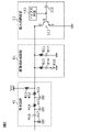
- FIG. 1 is a circuit configuration diagram of a high-frequency circuit and a communication device according to an embodiment.
- FIG. 2 is a circuit configuration diagram of a power amplifier circuit, a harmonic termination circuit, and a matching circuit according to the embodiment.
- FIG. 3 is a diagram showing a first specific example of frequency bands that can be used in the embodiment.
- FIG. 4 is a diagram showing a second specific example of frequency bands that can be used in the embodiment.
- FIG. 5 is a diagram showing a third specific example of frequency bands that can be used in the embodiment.
- FIG. 6 is a diagram showing the flow of signals in the high-frequency circuit according to the embodiment.
- FIG. 7 is a diagram showing the flow of signals in the high-frequency circuit according to the embodiment.
- FIG. 8 is a circuit configuration diagram of a harmonic termination circuit in a modified example of the embodiment.
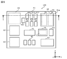
- 9 is a plan view of the high-frequency module according to the first embodiment.
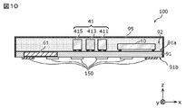
- FIG. FIG. 10 is a cross-sectional view of a high-frequency module according to Example 1.
- FIG. 11 is a plan view of a high frequency module according to Example 2.
- FIG. 12 is a plan view of a high frequency module according to Example 3.
- each drawing is a schematic diagram that has been appropriately emphasized, omitted, or adjusted in proportion to show the present invention, and is not necessarily strictly illustrated, and the actual shape, positional relationship, and ratio may differ.
- substantially the same configurations are denoted by the same reference numerals, and redundant description may be omitted or simplified.
- the x-axis and the y-axis are axes orthogonal to each other on a plane parallel to the main surface of the module substrate.
- the x-axis is parallel to the first side of the module substrate
- the y-axis is parallel to the second side orthogonal to the first side of the module substrate.
- the z-axis is an axis perpendicular to the main surface of the module substrate, and its positive direction indicates an upward direction and its negative direction indicates a downward direction.
- connection includes not only direct connection with connection terminals and/or wiring conductors, but also electrical connection via other circuit elements.
- Directly connected means directly connected by connection terminals and/or wiring conductors without intervening other circuit elements.
- Connected between A and B means connected to both A and B between A and B, in addition to being connected in series with the path connecting A and B , is connected between the path and ground.
- planar view means viewing an object by orthographic projection from the positive side of the z-axis onto the xy plane.
- a overlaps B in plan view means that the area of A orthogonally projected onto the xy plane overlaps the area of B orthogonally projected onto the xy plane.
- a is arranged between B and C means that at least one of a plurality of line segments connecting any point in B and any point in C passes through A.
- terms such as “parallel” and “perpendicular” that indicate the relationship between elements, terms that indicate the shape of elements such as “rectangular”, and numerical ranges do not represent only strict meanings, It means that an error of a substantially equivalent range, for example, several percent, is also included.
- the component is arranged on the main surface of the board means that the component is arranged on the main surface in contact with the main surface of the board, and that the component is arranged on the main surface without contacting the main surface. It includes being arranged above the surface and being arranged such that a part of the component is embedded in the substrate from the main surface side.
- FIG. 1 is a circuit configuration diagram of a high-frequency circuit 1 and a communication device 5 according to this embodiment.
- a communication device 5 includes a high frequency circuit 1, an antenna 2, an RFIC (Radio Frequency Integrated Circuit) 3, and a BBIC (Baseband Integrated Circuit) 4.
- RFIC Radio Frequency Integrated Circuit
- BBIC Baseband Integrated Circuit
- the high frequency circuit 1 transmits high frequency signals between the antenna 2 and the RFIC 3 .
- the internal configuration of the high frequency circuit 1 will be described later.
- the antenna 2 is connected to the antenna connection terminal 101 of the high frequency circuit 1, receives a high frequency signal from the outside and outputs it to the high frequency circuit 1.
- the RFIC 3 is an example of a signal processing circuit that processes high frequency signals. Specifically, the RFIC 3 performs signal processing such as up-conversion on the transmission signal input from the BBIC 4 , and outputs the high-frequency transmission signal generated by the signal processing to the transmission path of the high-frequency circuit 1 . Further, the RFIC 3 has a control section that controls the switches, amplifiers, etc. of the high-frequency circuit 1 . Some or all of the functions of the RFIC 3 as a control unit may be implemented outside the RFIC 3, for example, in the BBIC 4 or the high frequency circuit 1. FIG.
- the BBIC 4 is a baseband signal processing circuit that performs signal processing using an intermediate frequency band that is lower in frequency than the high frequency signal transmitted by the high frequency circuit 1 .
- Signals processed by the BBIC 4 include, for example, image signals for image display and/or audio signals for calling through a speaker.
- the antenna 2 and the BBIC 4 are not essential components in the communication device 5 according to the present embodiment.
- the high frequency circuit 1 includes power amplifier circuits 11 and 12, matching circuits (MN) 41 and 42, switch circuits 51 and 52, filter circuits 61 to 63, a control circuit 71, an antenna A connection terminal 101 , high-frequency input terminals 110 and 120 , and a control terminal 130 are provided.
- MN matching circuits
- the antenna connection terminal 101 is connected to the antenna 2 outside the high frequency circuit 1 .
- Each of the high frequency input terminals 120 and 130 is a terminal for receiving a high frequency transmission signal from the outside of the high frequency circuit 1 .
- the high frequency input terminals 110 and 120 are connected to the RFIC 3 outside the high frequency circuit 1 .
- the control terminal 130 is a terminal for transmitting control signals. That is, the control terminal 130 is a terminal for receiving a control signal from the outside of the high frequency circuit 1 and/or a terminal for supplying a control signal to the outside of the high frequency circuit 1 .
- a control signal is a signal relating to control of an electronic circuit included in the high-frequency circuit 1 .
- the control signal is a digital signal for controlling the power amplifier circuits 11 and 12 and the switch circuits 51 and 52, for example.
- the power amplifier circuit 11 can amplify transmission signals in the first frequency band and the second frequency band. As shown in FIG. 1, power amplifier circuit 11 is connected between high frequency input terminal 110 and filter circuits 61 and 62 . Specifically, the input terminal of the power amplifier circuit 11 is connected to the high frequency input terminal 110 . On the other hand, the output terminal of the power amplifier circuit 11 is connected to the filter circuit 61 or 62 via the harmonic termination circuit 81, the matching circuit 41 and the switch circuit 51. FIG.
- the power amplifier circuit 12 can amplify the transmission signal of the third frequency band. As shown in FIG. 1, power amplifier circuit 12 is connected between high frequency input terminal 120 and filter circuit 63 . Specifically, the input end of the power amplifier circuit 12 is connected to the high frequency input terminal 120 . On the other hand, the output terminal of the power amplifier circuit 12 is connected to the filter circuit 63 via the matching circuit 42 .
- the matching circuit 41 is connected between the power amplifier circuit 11 and the filter circuits 61 and 62 . Specifically, the matching circuit 41 is connected to the output terminal of the power amplifier circuit 11 via the harmonic termination circuit 81 and to the input terminals of the filter circuits 61 and 62 via the switch circuit 51 .
- the matching circuit 41 is an impedance matching circuit, and can match the output impedance (eg, 4 ohms) of the power amplifier circuit 11 and the input impedance (eg, 50 ohms) of the switch circuit 51 .
- the matching circuit 42 is connected between the power amplifier circuit 12 and the filter circuit 63 . Specifically, the matching circuit 42 is connected to the output terminal of the power amplifier circuit 12 and to the input terminal of the filter circuit 63 .
- the matching circuit 42 is an impedance matching circuit and can match the output impedance of the power amplifier circuit 12 and the input impedance of the filter circuit 63 .
- the switch circuit 51 is an example of a first switch circuit, and is connected between the output terminal of the power amplifier circuit 11 and the input terminals of the filter circuits 61 and 62 .
- the switch circuit 51 has terminals 511-513.
- a terminal 511 is an example of a first terminal and is connected to the output terminal of the power amplifier circuit 11 via the matching circuit 41 and the harmonic termination circuit 81 .
- a terminal 512 is an example of a second terminal and is connected to the input terminal of the filter circuit 61 .
- a terminal 513 is an example of a third terminal and is connected to the input end of the filter circuit 62 .
- the switch circuit 51 is composed of, for example, an SPDT (Single-Pole Double-Throw) type switch circuit, and is sometimes called a band select switch.
- SPDT Single-Pole Double-Throw
- the switch circuit 51 can connect the terminal 511 to either one of the terminals 512 and 513 based on a control signal from the RFIC 3, for example. That is, the switch circuit 51 can switch the connection destination of the output terminal of the power amplifier circuit 11 between the filter circuits 61 and 62 . For example, the switch circuit 51 connects the terminal 511 to the terminal 512 in a state where the terminal 521 is connected to the terminal 522 in the switch circuit 52 . On the other hand, in the state where the terminal 521 is connected to the terminal 523 in the switch circuit 52 , the switch circuit 51 connects the terminal 511 to the terminal 513 .
- the switch circuit 52 is an example of a second switch circuit, and is connected between the antenna connection terminal 101 and the filter circuits 61-63.
- the switch circuit 52 has terminals 521-524.
- Terminal 521 is an example of a fourth terminal and is connected to antenna connection terminal 101 .
- a terminal 522 is an example of a fifth terminal and is connected to the output end of the filter circuit 61 .
- a terminal 523 is an example of a sixth terminal and is connected to the output terminal of the filter circuit 62 .
- a terminal 524 is an example of a seventh terminal and is connected to the output terminal of the filter circuit 63 .
- the switch circuit 52 is composed of, for example, a multi-connection switch circuit, and is sometimes called an antenna switch.
- the switch circuit 52 can connect the terminal 521 to at least one of the terminals 522 to 524 based on the control signal from the RFIC 3, for example. That is, the switch circuit 52 switches between connection and non-connection of the antenna connection terminal 101 and the filter circuit 61, switches between connection and non-connection of the antenna connection terminal 101 and the filter circuit 62, and connects and disconnects the antenna connection terminal 101 and the filter circuit 63. Disconnection can be toggled.
- the filter circuit 61 is an example of a first filter circuit, has a passband including the first frequency band, and is composed of an LC filter.
- Filter circuit 61 is connected between power amplifier circuit 11 and antenna connection terminal 101 .
- the input terminal of the filter circuit 61 is connected to the output terminal of the power amplifier circuit 11 via the switch circuit 51 , the matching circuit 41 and the harmonic termination circuit 81 .
- the output terminal of the filter circuit 61 is connected to the antenna connection terminal 101 via the switch circuit 52 .
- the filter circuit 61 can pass the transmission signal in the first frequency band amplified by the power amplifier circuit 11 .
- An LC filter is a circuit that is composed of inductors and capacitors and has the function of passing or blocking signals in a specific frequency band. LC filters do not include acoustic wave elements.
- the filter circuit 62 is an example of a second filter circuit, has a passband including a second frequency band that at least partially overlaps with the first frequency band, and is composed of an elastic wave filter.
- Filter circuit 62 is connected between power amplifier circuit 11 and antenna connection terminal 101 .
- the input terminal of the filter circuit 62 is connected to the output terminal of the power amplifier circuit 11 via the switch circuit 51 , the matching circuit 41 and the harmonic termination circuit 81 .
- the output terminal of the filter circuit 62 is connected to the antenna connection terminal 101 via the switch circuit 52 . Thereby, the filter circuit 62 can pass the transmission signal of the second frequency band amplified by the power amplifier circuit 11 .
- An elastic wave filter is a circuit that is configured with an elastic wave element and has a function of passing or blocking signals in a specific frequency band.
- Acoustic wave filters may include inductors and/or capacitors.
- the filter circuit 63 is an example of a third filter circuit and has a passband including the third frequency band.
- Filter circuit 63 is connected between power amplifier circuit 12 and antenna connection terminal 101 .
- the input terminal of the filter circuit 63 is connected to the output terminal of the power amplifier circuit 12 .
- the output end of the filter circuit 63 is connected to the antenna connection terminal 101 via the switch circuit 52 .
- the filter circuit 63 can pass the transmission signal of the third frequency band amplified by the power amplifier circuit 12 .
- the control circuit 71 is a power amplifier controller that controls the power amplifier circuit 11 .
- the control circuit 71 receives a control signal from the RFIC 3 via the control terminal 130 and outputs the control signal to the power amplifier circuit 11 .
- the harmonic termination circuit 81 is connected between the power amplifier circuit 11 and the matching circuit 41, and arranged in a low-impedance path.
- the harmonic termination circuit 81 has a function of attenuating harmonic bands that are integral multiples (for example, two times) of the first frequency band and the second frequency band.
- the harmonic termination circuit 81 also has a function of adjusting the output waveform of the power amplifier circuit 11 and improving the efficiency of the power amplifier circuit 11 .
- the band attenuated by the harmonic termination circuit 81 is not limited to the harmonic bands of the first frequency band and the second frequency band.
- the harmonic termination circuit 81 has a function of attenuating a frequency band that is higher than the first frequency band and the second frequency band and is not a harmonic band of the first frequency band and the second frequency band. may
- the high frequency circuit 1 does not have to include the power amplifier circuit 12, the matching circuit 42, the switch circuit 52, the filter circuit 63, and the control circuit 71.
- FIG. 2 is a circuit configuration diagram of the power amplifier circuit 11, the harmonic termination circuit 81 and the matching circuit 41 in this embodiment.
- the power amplifier circuit 11 includes an amplifier transistor 111, a capacitor 112, and a bias circuit 113.
- the amplification transistor 111 is a bipolar transistor having a collector, emitter and base.
- the base, collector and emitter of the amplification transistor 111 are connected to the input terminal and output terminal of the power amplifier circuit 11 and to the ground, respectively.
- the amplification transistor 111 can amplify the high-frequency current input to the base and output it from the collector.
- the amplification transistor 111 may be a field effect transistor having a drain, a source and a gate.
- Capacitor 112 is connected between the base of the amplification transistor 111 and the input terminal of the power amplification circuit 11 .
- Capacitor 112 is a capacitive element for cutting DC, and has a function of preventing DC current from leaking to the input end of power amplifier circuit 11 due to DC bias voltage applied to the base from bias circuit 113 .
- the bias circuit 113 is connected to the base of the amplification transistor 111 .
- the bias circuit 113 has a function of optimizing the operating point of the amplification transistor 111 by supplying a bias signal to the base of the amplification transistor 111 .
- the input signal becomes a base current flowing from the base to the emitter of the amplification transistor 111 .
- the base current is amplified by the amplification transistor 111 and becomes a collector current.
- An output signal corresponding to the collector current is then output.
- power amplifier circuit 11 may be a multi-stage amplifier circuit having a plurality of serially connected amplifier transistors. Further, the power amplifier circuit 11 may be a differential amplifier circuit or a Doherty amplifier circuit.
- harmonic termination circuit 81 includes inductors 811 and 813 , capacitors 812 and 814 and switch 815 .
- inductor 811 and the capacitor 812 are connected in series to a parallel arm path that connects the path connecting the power amplifier circuit 11 and the matching circuit 41 to the ground, and constitute an LC resonance circuit.
- inductor 811 and capacitor 812 have the function of adjusting the waveform of the output signal of power amplifier circuit 11 .
- inductor 811 and capacitor 812 may function to attenuate harmonics in the first frequency band and/or the second frequency band.
- the inductor 813 and the capacitor 814 are examples of a first inductor and a first capacitor, respectively.
- the inductor 813 and the capacitor 814 are connected in series to a first parallel arm path that connects the path connecting the power amplifier circuit 11 and the matching circuit 41 to the ground, forming an LC resonance circuit.
- inductor 813 and capacitor 814 have the function of attenuating a harmonic band that is an integer multiple (for example, twice) the second frequency band.
- inductor 813 and capacitor 814 may have a function of adjusting the waveform of the output signal of power amplifier circuit 11 .
- the inductor 813 and the capacitor 814 may have a function of attenuating a band different from the harmonic band for the first frequency band and the second frequency band.
- the inductor 813 and the capacitor 814 have a function of attenuating a frequency band that is higher than the first frequency band and the second frequency band and is not a harmonic band of the first frequency band and the second frequency band.
- the LC resonant circuit composed of the inductor 813 and capacitor 814 is arranged in the parallel arm path of the low impedance system, it functions as an attenuation pole with a low Q value and can attenuate signals in a wide band.
- a switch 815 is an example of a first switch and is connected in series with an inductor 813 and a capacitor 814 .
- Switch 815 can turn on/off the first parallel arm path to which inductor 813 and capacitor 814 are connected. For example, with the filter circuit 62 connected to the antenna connection terminal 101 and the power amplifier circuit 11, the switch 815 is turned on. Conversely, when the filter circuit 61 is connected to the antenna connection terminal 101 and the power amplifier circuit 11, the switch 815 is turned off. Here, the switch 815 is connected closer to the ground than the inductor 813 and the capacitor 814 are.
- harmonic termination circuit 81 is not limited to the configuration of FIG.
- harmonic termination circuit 81 may not have a parallel arm path to which inductor 811 and capacitor 812 are connected.
- the capacitor 812 is connected to the ground side rather than the inductor 811, but the inductor 811 may be connected to the ground side rather than the capacitor 812.
- the inductor 813, the capacitor 814 and the switch 815 are connected in this order toward the ground side, but the order of the inductor 813, the capacitor 814 and the switch 815 is not limited to this.
- the order of inductor 813 and capacitor 814 may be swapped
- the order of inductor 813 and switch 815 may be swapped
- the order of capacitor 814 and switch 815 may be swapped.
- matching circuit 41 includes inductors 411 , 412 and 414 , capacitors 413 , 415 and 416 and resistor 417 .
- the inductor 411 is connected to a power supply path for supplying the power supply voltage Vcc.
- Inductors 412 and 414 and capacitor 416 are connected in series in a high frequency signal path that carries high frequency signals.
- Capacitors 413 and 415 and resistor 417 are respectively connected between the high frequency signal path and ground.
- the matching circuit 41 can match the output impedance (low impedance) of the power amplifier circuit 11 and the input impedance (reference impedance) of the switch circuit 51 by means of inductors, capacitors, etc. connected in this manner.
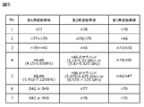
- FIG. 3 to 5 are diagrams showing first to third specific examples of frequency bands that can be used in this embodiment. 3 and 4 show graphs representing the pass characteristics of the filter circuit.
- the filter circuit 62 made up of an elastic wave filter realizes a steeper transition from the passband to the stopband than the filter circuit 61 made up of an LC filter. be able to.
- the filter circuit 61 can achieve higher attenuation than the filter circuit 62 in a band (for example, harmonic band) away from the passband.
- the filter circuit 61 can achieve a lower loss than the filter circuit 62 in the passband.
- the steepness of the transition from the passband to the stopband can be specified by measuring the gain at a frequency separated by a predetermined frequency (100 MHz in this embodiment) from the cutoff frequency (end of the passband). . At this time, the smaller the measured gain, the higher the steepness.
- the cutoff frequency is defined as the frequency at which the output is -3 dB of the output in the passband.
- the same band for 5GNR (5th Generation New Radio) is used as the first frequency band and the second frequency band. That is, the first frequency band and the second frequency band match.
- both n77 for 5GNR are used as the first and second frequency bands
- n79 for 5GNR is used as the third frequency band.
- a band for 5GNR means a frequency band predefined for 5GNR by 3GPP (3rd Generation Partnership Project).
- the filter circuits 61 and 62 may be switched according to power class. That is, the switch circuit 51 connects the terminal 511 to the terminal 512 when the signal of the first frequency band (that is, the second frequency band) is transmitted in the first power class, and ) is transmitted in a second power class having a lower maximum output power than the first power class, terminal 511 may be connected to terminal 513 .
- the power class is a classification of terminal output power defined by maximum output power, etc., and the smaller the power class value, the higher the power output.
- the maximum output power for power class 1 is 31 dBm
- the maximum output power for power class 1.5 is 29 dBm
- the maximum output power for power class 2 is 26 dBm
- the maximum output power for power class 3 is 23 dBm. .
- the terminal's maximum output power is defined as the output power at the terminal's antenna end. Measurement of the maximum output power of the terminal is performed, for example, by a method defined by 3GPP or the like. For example, in FIG. 1 the maximum output power is measured by measuring the radiated power at antenna 2 . Instead of measuring the radiation power, it is also possible to measure the output power of the antenna 2 by providing a terminal near the antenna 2 and connecting a measuring instrument (such as a spectrum analyzer) to the terminal.
- a measuring instrument such as a spectrum analyzer
- a band for 5GNR and subbands within the band are used as the first frequency band and the second frequency band, respectively. That is, the second frequency band is included in the first frequency band. In other words, the entire second frequency band overlaps part of the first frequency band.
- the table of FIG. 1 uses n77 for 5GNR and its subbands as the first and second frequency bands, respectively, and n79 for 5GNR as the third frequency band.
- a subband means a band obtained by dividing a band for a communication system.
- band n77 for 5GNR is assigned by multiple Mobile Network Operators (MNOs).
- MNOs Mobile Network Operators
- 3600-3700 MHz is assigned a first MNO
- 3700-3800 MHz is assigned a second MNO
- 3800-3900 MHz is assigned a third MNO
- 3900-4000 MHz is assigned a fourth MNO
- 4000-4100 MHz is again assigned a second MNO. assigned.
- the portion of n77 assigned to each MNO can be used as a subband.
- the sub-bands need not be limited to the bands to which the MNO is assigned.
- different bands for 5GNR are used as the first frequency band and the second frequency band, or bands or channels for 5GNR and WLAN (Wireless Local Area Network) are used respectively.
- the second frequency band at least partially overlaps with the first frequency band.
- n77 and n78 for 5GNR are used as the first and second frequency bands, respectively, and n79 for 5GNR is used as the third frequency band.
- the first frequency band is wider than the second frequency band.
- a band for WLAN means a frequency band or channel predefined for WLAN by the Institute of Electrical and Electronics Engineers (IEEE).
- first to third frequency bands shown in FIGS. 3 to 5 are examples and are not limited to these.
- the first frequency band and the second frequency band may be interchanged.
- n78 for 5GNR may be used as the first frequency band
- n77 for 5GNR may be used as the second frequency band.
- the first frequency band is narrower than the second frequency band.
- FIG. 6 and 7 are diagrams showing signal flows in the high-frequency circuit 1 according to the embodiment.
- the switch circuit 52 cannot connect the terminal 521 to the terminal 524 when the terminal 521 is connected to the terminal 522, and connects the terminal 521 to the terminal 524 when the terminal 521 is connected to the terminal 523. It is possible.
- the RFIC 3 can realize the first connection state shown in FIG. 6 by controlling each switch circuit of the high frequency circuit 1 .
- the switch circuit 51 connects the terminal 511 to the terminal 512 and the switch circuit 52 connects the terminal 521 to the terminal 522 .
- switch 815 of harmonic termination circuit 81 is turned off.
- the fundamental wave of the input signal of the high-frequency circuit 1 passes through the high-frequency input terminal 110, the power amplifier circuit 11, the harmonic termination circuit 81, the matching circuit 41, the switch circuit 51, the filter circuit 61, and the switch circuit 52. It flows to the antenna connection terminal 101 . Also, the harmonics of the input signal flow to the ground via the inductor 811 and the capacitor 812 in the harmonic termination circuit 81, but do not flow to the ground via the inductor 813 and the capacitor 814.
- the RFIC 3 can also realize the second connection state of FIG. 7 by controlling each switch circuit of the high frequency circuit 1 .
- switch circuit 51 connects terminal 511 to terminal 513 and switch circuit 52 connects terminal 521 to terminals 523 and 524 .
- switch 815 of harmonic termination circuit 81 is turned on.
- one of the fundamental waves of the two input signals of the high frequency circuit 1 is transferred from the high frequency input terminal 110 to the power amplifier circuit 11, the harmonic termination circuit 81, the matching circuit 41, the switch circuit 51, the filter circuit 62 and the switch circuit 52. through the antenna connection terminal 101 .
- the harmonic of one of the two input signals flows through inductor 811 and capacitor 812 to ground in harmonic termination circuit 81 and through inductor 813 , capacitor 814 and switch 815 to ground.
- a first power supply voltage (Vcc) applied to the power amplifier circuit 11 in the first connection state of FIG. 6 and a second power supply voltage (Vcc) applied to the power amplifier circuit 11 in the second connection state of FIG. may have voltage values different from each other.
- the second power supply voltage may be higher than the first power supply voltage.
- the first bias signal supplied to the power amplifier circuit 11 in the first connection state of FIG. 6 and the second bias signal supplied to the power amplifier circuit 11 in the second connection state of FIG. It may have a value or a voltage value.
- the current value of the second bias signal may be greater than the current value of the first bias signal.
- the voltage value of the second bias signal may be greater than the voltage value of the first bias signal.
- the high-frequency circuit 1 has the power amplifier circuit 11, the matching circuit 41 connected to the power amplifier circuit 11, and the passband including the first frequency band. and a filter circuit 62 having a pass band including a second frequency band at least partially overlapping with the first frequency band, and configured by an acoustic wave filter, and a matching circuit 41 to transmit the electric power.
- a switch circuit 51 having a terminal 511 connected to the amplifier circuit 11, a terminal 512 connected to the filter circuit 61, and a terminal 513 connected to the filter circuit 62, and a path connecting the power amplifier circuit 11 and the matching circuit 41.
- a harmonic termination circuit 81 having an inductor 813, a capacitor 814, and a switch 815 connected in series to a first parallel arm path connecting to ground.
- an inductor 813, a capacitor 814, and a switch 815 connected in series to a first parallel arm path connecting the path connecting the power amplifier circuit 11 and the matching circuit 41 to the ground are arranged. Therefore, since the LC series circuit is arranged in the parallel arm path of the output impedance (that is, low impedance) system of the power amplifier circuit 11, the LC series circuit can function as an attenuation pole having a low Q value. Therefore, the harmonic termination circuit 81 can achieve broadband attenuation and improve signal quality. Moreover, since the switch 815 is connected to the LC series circuit included in the harmonic termination circuit 81, attenuation by the harmonic termination circuit 81 can be changed according to the attenuation characteristics of the filter used.
- the switch 815 of the harmonic termination circuit 81 is turned off when the switch circuit 51 connects the terminal 511 to the terminal 512, and the switch circuit 51 connects the terminal 511 to the terminal 512. It may be turned on while connected to the terminal 513 .
- the switch 815 of the harmonic termination circuit 81 is turned on when the filter circuit 62 composed of an elastic wave filter is connected to the power amplifier circuit 11 .
- Acoustic filters tend to lack attenuation in bands far from the passband than LC filters. Therefore, by turning on the switch 815 when the elastic wave filter is used, the harmonic termination circuit 81 can reinforce the attenuation that is insufficient in the elastic wave filter in a wide band, thereby improving the signal quality. can be planned.
- the harmonic termination circuit 81 can give priority to the waveform adjustment of the output signal of the power amplifier circuit 11, and the efficiency of the power amplifier circuit 11 can be improved. can be improved.
- the switch 815 may be connected closer to the ground than the inductor 813 and the capacitor 814 are.
- the switch 815 is composed of a field-effect transistor (FET)
- FET field-effect transistor
- the source of the FET can be grounded. Therefore, when a voltage is applied to the gate of the FET to turn on the switch 815, the potential difference between the gate and the source can be increased, and the impedance between the drain and the source can be decreased.
- the first frequency band is equal to the second frequency band
- the switch circuit 51 transmits the signals of the first frequency band and the second frequency band in the first power class.
- terminal 511 is connected to terminal 512
- terminal 511 is connected to terminal 513 when signals in the first and second frequency bands are transmitted in a second power class having a smaller maximum output power than the first power class. may be connected to
- an LC filter can be used when a high-frequency signal with higher power is transmitted.
- LC filters have higher power durability than acoustic wave filters. Therefore, a high-frequency signal can be transmitted using a filter circuit more suitable for the power class, and the quality of the transmission signal can be improved.
- the high-frequency circuit 1 includes a filter circuit 63 having a passband including a third frequency band that does not overlap with the first frequency band and the second frequency band, and a terminal connected to the antenna connection terminal 101. 521 , a terminal 522 connected to the filter circuit 61 , a terminal 523 connected to the filter circuit 62 , and a switch circuit 52 having a terminal 524 connected to the filter circuit 63 .
- the high-frequency circuit 1 can transmit signals in the third frequency band in addition to the first frequency band and the second frequency band.
- the switch circuit 51 connects the terminal 511 to the terminal 512 in a state in which the terminal 521 is connected to the terminal 522 in the switch circuit 52 , and the switch circuit 52 connects the terminal 521 to the terminal 522 .
- the terminal 511 may be connected to the terminal 513 .
- the filter circuits 61 and 62 connected to the path connecting the power amplifier circuit 11 and the antenna connection terminal 101 can be switched.
- the switch circuit 52 cannot connect the terminal 521 to the terminal 524 when the terminal 521 is connected to the terminal 522, and the terminal 521 is connected to the terminal 523. In the closed state, terminal 521 may be connectable to terminal 524 .
- the filter circuit 61 is composed of an elastic wave filter instead of the filter circuit 61 composed of an LC filter.
- the filter circuit 62 can be connected to the path connecting the power amplifier circuit 11 and the antenna connection terminal 101 . Therefore, even when the third frequency band is located near the first frequency band and the second frequency band, the filter circuit 62 can ensure attenuation of the third frequency band, and the signal of the third frequency band can be and signals in the first and second frequency bands simultaneously.
- the first frequency band is one of n77 and n78 for 5GNR
- the second frequency band is the other of n77 and n78 for 5GNR.
- the third frequency band may be n79 for 5GNR.
- the first frequency band may be narrower than the second frequency band.
- the first frequency band may be wider than the second frequency band.
- the high frequency circuit 1 can be used for transmitting the signals of n77, n78 and n79 for 5GNR.
- the first power supply voltage is applied to the power amplifier circuit 11 in a state in which the terminal 511 is connected to the terminal 512 in the switch circuit 51, and the terminal 511 is connected to the terminal 512 in the switch circuit 51.
- a second power supply voltage higher than the first power supply voltage may be applied to the power amplifier circuit 11 .
- the filter circuit 62 configured by the acoustic wave filter when the filter circuit 62 configured by the acoustic wave filter is connected to the power amplifier circuit 11, the power supply is more efficient than the case where the filter circuit 61 configured by the LC filter is connected to the power amplifier circuit 11. Voltage can be increased.
- acoustic wave filters have a greater loss in the passband than LC filters, so the power amplifier circuit 11 is required to have higher output power than LC filters. Therefore, when the filter circuit 62 is connected to the power amplifier circuit 11, a higher power supply voltage is applied to the power amplifier circuit 11, thereby meeting the demand for higher output power.
- the first bias signal is supplied to the power amplifier circuit 11 in a state in which the terminal 511 is connected to the terminal 512 in the switch circuit 51, and the terminal 511 is connected to the terminal 512 in the switch circuit 51.
- the second bias signal is supplied to the power amplifier circuit 11, and the current value of the second bias signal is greater than the current value of the first bias signal, or the voltage value of the second bias signal is the second bias signal. It may be greater than the voltage value of the 1 bias signal.
- the bias voltage is lower than when the filter circuit 61 configured by the LC filter is connected to the power amplifier circuit 11.
- the current value or voltage value of the signal can be increased.
- acoustic wave filters have a greater loss in the passband than LC filters, so the power amplifier circuit 11 is required to have higher output power than LC filters. Therefore, when the filter circuit 62 is connected to the power amplifier circuit 11, a bias signal having a larger current value or voltage value is supplied to the power amplifier circuit 11, thereby meeting the demand for higher output power. can.
- a communication device 5 includes an RFIC 3 that processes high frequency signals, and a high frequency circuit 1 that transmits high frequency signals between the RFIC 3 and the antenna 2 .
- the communication device 5 can achieve the same effect as the high-frequency circuit 1 described above.
- the high-frequency circuit 1 includes a harmonic termination circuit 81A instead of the harmonic termination circuit 81 shown in FIG.
- the circuit configuration of the harmonic termination circuit 81A will be described with reference to FIG.
- FIG. 8 is a circuit configuration diagram of a harmonic termination circuit 81A in this modified example.
- the harmonic termination circuit 81A according to this modification includes inductors 811, 813 and 816, capacitors 812, 814 and 817, and switches 815 and 818.
- the inductor 816 and the capacitor 817 are examples of a second inductor and a second capacitor, respectively.
- the inductor 816 and the capacitor 817 are connected in series to a second parallel arm path that connects the path connecting the power amplifier circuit 11 and the matching circuit 41 to the ground, forming an LC resonance circuit.
- inductor 816 and capacitor 817 have the function of attenuating harmonic bands that are integral multiples (for example, twice) of the first frequency band and/or the second frequency band.
- the resonance frequency of inductor 816 and capacitor 817 may be different from the resonance frequency of inductor 813 and capacitor 814 .
- inductor 816 and capacitor 817 may have the function of adjusting the waveform of the output signal of power amplifier circuit 11 .
- the inductor 816 and the capacitor 817 may have a function of attenuating a band different from the harmonic band for the first frequency band and the second frequency band.
- the inductor 816 and the capacitor 817 have a function of attenuating a frequency band that is higher than the first frequency band and the second frequency band and is not a harmonic band of the first frequency band and the second frequency band.
- the switch 818 is an example of a second switch, and can switch on/off the second parallel arm path that connects the path connecting the power amplifier circuit 11 and the matching circuit 41 to the ground. For example, when the filter circuit 61 is connected to the antenna connection terminal 101 and the power amplifier circuit 11, the switch 818 is turned off, and when the filter circuit 62 is connected to the antenna connection terminal 101 and the power amplifier circuit 11, the switch 818 is turned on. Here, the switch 818 is connected closer to ground than the inductor 816 and capacitor 817 are.
- the inductor 816 and the capacitor 817 are arranged in the parallel arm path of the low impedance system, they function as attenuation poles with a low Q value and can attenuate signals over a wide band.
- harmonic termination circuit 81A is not limited to the configuration of FIG.
- harmonic termination circuit 81A may not include inductor 811 and capacitor 812.
- FIG. the inductor 816, the capacitor 817 and the switch 818 are connected in this order toward the ground side, but the order of the inductor 816, the capacitor 817 and the switch 818 is not limited to this.
- the order of inductor 816 and capacitor 817 may be swapped
- the order of inductor 816 and switch 818 may be swapped
- the order of capacitor 817 and switch 818 may be swapped.
- the harmonic termination circuit 81A includes the inductor 816 connected in series to the second parallel arm path connecting the path connecting the power amplifier circuit 11 and the matching circuit 41 and the ground. , capacitor 817 and switch 818 .
- the attenuation by the harmonic termination circuit 81A can be changed more flexibly according to the attenuation characteristics of the filter used. can be done.
- the switch 818 of the harmonic termination circuit 81A is turned off when the switch circuit 51 connects the terminal 511 to the terminal 512, and the switch circuit 51 connects the terminal 511 to the terminal 512. It may be turned on while connected to the terminal 513 .
- the switch 818 of the harmonic termination circuit 81A when the filter circuit 62 configured by the acoustic wave filter is connected to the power amplifier circuit 11, the switch 818 of the harmonic termination circuit 81A is turned on. Acoustic filters tend to lack attenuation in bands farther from the passband than LC filters. Therefore, by turning on the switch 818 when an acoustic wave filter is used, the harmonic termination circuit 81A can reinforce the attenuation that is insufficient in the acoustic wave filter over a wide band. On the other hand, by turning off the switch 818 when the LC filter is used, the harmonic termination circuit 81A can prioritize the waveform adjustment of the output signal of the power amplifier circuit 11, and the efficiency of the power amplifier circuit 11 can be improved. can be improved.
- the switch 818 may be connected closer to the ground than the inductor 816 and the capacitor 817.
- the switch 818 when the switch 818 is composed of an FET, the source of the FET can be connected to the ground. Therefore, when a voltage is applied to the gate of the FET to turn on the switch 818, the potential difference between the gate and the source can be increased, and the impedance between the drain and the source can be decreased.
- the on/off control of the switches 815 and 818 is not limited to this.
- one of the switches 815 and 818 of the harmonic termination circuit 81A may be turned on and the other of the switches 815 and 818 may be turned off in a given state.
- the switch 815 in a state in which the filter circuit 61 is connected to the antenna connection terminal 101 and the power amplifier circuit 11, the switch 815 is turned off, the switch 818 is turned on, and the filter circuit 62 is connected to the antenna connection terminal. 101 and the power amplifier circuit 11, the switch 815 may be turned on and the switch 818 may be turned off.
- inductor 813 and capacitor 814 connected to the first parallel arm path ensure attenuation of harmonics of the signal in the first frequency band
- inductor 817 and capacitor 818 connected to the second parallel arm path ensure attenuation of the second harmonic. Attenuation of harmonics of the signal in the frequency band can be ensured.
- Example 1 Next, as Example 1 of the high frequency circuit 1 according to the above embodiment, a high frequency module 100 in which the high frequency circuit 1 is mounted will be described with reference to FIGS. 9 and 10.
- FIG. 9 Example 1 of the high frequency circuit 1 according to the above embodiment
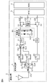
- FIG. 9 is a plan view of the high frequency module 100 according to this embodiment.
- FIG. 10 is a cross-sectional view of a high frequency module 100 according to this embodiment. The cross section of the high frequency module 100 in FIG. 10 is taken along line xx in FIG.
- illustration of wiring for connecting a plurality of components arranged on the module substrate 91 is omitted except for some.
- illustration of the resin member 92 and the shield electrode layer 95 covering the main surface 91a of the module substrate 91 is omitted.
- the high-frequency module 100 further includes a module substrate 91, a resin member 92, a shield electrode layer 95, and a plurality of external connection terminals 150, in addition to the circuit components including the circuit elements shown in FIG.
- the module substrate 91 has main surfaces 91a and 91b facing each other.
- the module substrate 91 has a rectangular shape in plan view, but the shape of the module substrate 91 is not limited to this.
- a low temperature co-fired ceramics (LTCC) substrate having a laminated structure of a plurality of dielectric layers, a high temperature co-fired ceramics (HTCC) substrate, A component-embedded substrate, a substrate having a redistribution layer (RDL), a printed substrate, or the like can be used, but is not limited to these.
- the main surface 91a is an example of a first main surface, and is sometimes called an upper surface or a front surface.
- the integrated circuits 10 and 70, the power amplifier circuit 12, the matching circuits 41 and 42, the switch circuits 51 and 52, and the filter circuits 61 to 63 are arranged on the main surface 91a.
- the integrated circuit 10 includes a power amplifier circuit 11 and a harmonic termination circuit 81.
- Integrated circuit 10 is composed of, for example, gallium arsenide (GaAs), silicon germanium (SiGe), or gallium nitride (GaN). In this case, a high-quality power amplifier circuit 11 can be realized.
- the integrated circuit 10 may be composed of, for example, CMOS (Complementary Metal Oxide Semiconductor), and specifically manufactured by an SOI (Silicon on Insulator) process. In this case, an inexpensive power amplifier circuit 11 can be realized.
- CMOS Complementary Metal Oxide Semiconductor
- the integrated circuit 70 includes a control circuit 71 .
- the integrated circuit 70 is composed of CMOS, for example, and may be specifically manufactured by an SOI process.
- the switch circuits 51 and 52 are composed of, for example, a plurality of MOSFETs (Metal-Oxide-Semiconductor Field-Effect Transistors) connected in series.
- MOSFETs Metal-Oxide-Semiconductor Field-Effect Transistors
- the number of stages of series connection of MOSFETs is not particularly limited as long as it is determined according to the required withstand voltage.
- the filter circuit 61 is composed of an LC filter including inductors and capacitors.
- the inductors and capacitors included in the LC filter are formed within the module substrate 91 .
- the filter circuit 61 may be mounted on the main surface 91a of the module substrate 91 as a plurality of surface mount components (SMD: Surface Mount Device).
- SMD Surface Mount Device
- the filter circuit 62 is composed of an acoustic wave filter (for example, a surface acoustic wave (SAW) filter or a bulk acoustic wave (BAW) filter).
- SAW surface acoustic wave
- BAW bulk acoustic wave
- the filter circuit 63 may be configured using, for example, any of a SAW filter, a BAW filter, an LC resonance filter, and a dielectric filter, and is not limited to these.
- the resin member 92 covers the main surface 91a and the components on the main surface 91a.
- the resin member 92 has a function of ensuring reliability such as mechanical strength and moisture resistance of the parts on the main surface 91a. Note that the resin member 92 may not be included in the high frequency module 100 .
- the shield electrode layer 95 is a metal thin film formed by sputtering, for example, and is formed so as to cover the top and side surfaces of the resin member 92 and the side surfaces of the module substrate 91 .
- the shield electrode layer 95 is set to a ground potential and suppresses external noise from entering the components that constitute the high frequency module 100 . Note that the shield electrode layer 95 may not be included in the high frequency module 100 .
- a plurality of external connection terminals 150 are arranged on the main surface 91b.
- the plurality of external connection terminals 150 include a ground terminal in addition to the antenna connection terminal 101, the high frequency input terminals 110 and 120, and the control terminal 130 shown in FIG.
- Each of the plurality of external connection terminals 150 is joined to an input/output terminal and/or a ground terminal or the like on a mother board arranged in the z-axis negative direction of the high frequency module 100 .
- bump electrodes can be used as the plurality of external connection terminals 150, but the invention is not limited to this.
- the component arrangement shown in FIGS. 9 and 10 is an example and is not limited to this.
- some or all of the components may be arranged on the main surface 91 b of the module substrate 91 .
- the main surface 91b and the components on the main surface 91b may be covered with a resin member.
- the switch circuits 51 and 52 may be integrated into one integrated circuit or may be included in the integrated circuit 70 .
- the inductors and/or capacitors included in the matching circuits 41 and 42 and the filter circuit 61 may not be made of SMD.
- the inductor and/or capacitor may comprise an Integrated Passive Device (IPD).
- IPD Integrated Passive Device
- the inductors and/or capacitors may be configured by wiring patterns within the module substrate 91 .
- the high-frequency module 100 includes the module substrate 91, the power amplifier circuit 11 arranged on the module substrate 91, and the matching circuit arranged on the module substrate 91 and connected to the power amplifier circuit 11. 41, a filter circuit 61 arranged on the module substrate 91, having a passband including the first frequency band and configured by an LC filter, and a filter circuit 61 arranged on the module substrate 91, at least partially overlapping the first frequency band.
- a filter circuit 62 configured by an acoustic wave filter having a passband including a second frequency band, a terminal 511 arranged on the module substrate 91 and connected to the power amplifier circuit 11 via the matching circuit 41, the filter A switch circuit 51 having a terminal 512 connected to the circuit 61 and a terminal 513 connected to the filter circuit 62 is arranged on the module substrate 91 to connect a path connecting the power amplifier circuit 11 and the matching circuit 41 to the ground.
- a harmonic termination circuit 81 having an inductor 813, a capacitor 814 and a switch 815 serially connected in the first parallel arm path. At this time, the harmonic termination circuit 81 and the power amplifier circuit 11 are included in one integrated circuit 10 .
- the harmonic termination circuit 81 and the power amplifier circuit 11 are integrated into one integrated circuit 10, which contributes to miniaturization of the high frequency module 100.
- the high-frequency circuit 1 according to the modified example can also be mounted on the high-frequency module 100 in the same manner as in the present embodiment.
- harmonic termination circuit 81A is included in integrated circuit 10 .
- Example 2 of the high-frequency circuit 1 according to the above embodiment will be described.
- the present embodiment is mainly different from the first embodiment in that the harmonic termination circuit 81 is included in the same integrated circuit as the control circuit 71 instead of the power amplifier circuit 11 .
- the radio frequency module according to the present embodiment will be described below with reference to FIG. 11, focusing on the differences from the first embodiment.
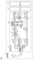
- FIG. 11 is a plan view of a high frequency module 100B according to this embodiment.
- the integrated circuits 10B and 70B are arranged on the main surface 91a of the module substrate 91.
- FIG. 11 is a plan view of a high frequency module 100B according to this embodiment.
- the integrated circuits 10B and 70B are arranged on the main surface 91a of the module substrate 91.
- the integrated circuit 10B includes the power amplifier circuit 11 and does not include the harmonic termination circuit 81.
- the integrated circuit 10B like the integrated circuit 10, is made of GaAs, SiGe, or GaN, for example. Also, the integrated circuit 10B may be composed of CMOS, for example, and specifically manufactured by an SOI process.
- the integrated circuit 70B includes a harmonic termination circuit 81 in addition to the control circuit 71.
- the integrated circuit 70B is composed of CMOS, for example, and may be specifically manufactured by an SOI process.
- the high-frequency module 100B includes the module substrate 91, the power amplifier circuit 11 arranged on the module substrate 91, and the control circuit 71 arranged on the module substrate 91 for controlling the power amplifier circuit 11. , a matching circuit 41 arranged on the module substrate 91 and connected to the power amplifier circuit 11, and a filter circuit 61 arranged on the module substrate 91, having a pass band including the first frequency band, and constituted by an LC filter.
- a harmonic termination circuit 81 having an inductor 813, a capacitor 814, and a switch 815 that are arranged and connected in series to a first parallel arm path that connects a path that connects the power amplifier circuit 11 and the matching circuit 41 to the ground.
- the harmonic termination circuit 81 and the control circuit 71 are included in one integrated circuit 70B.
- the harmonic termination circuit 81 and the control circuit 71 are integrated in one integrated circuit 70B, it is possible to contribute to miniaturization of the high frequency module 100B.
- the high-frequency circuit 1 according to the modified example can also be mounted on the high-frequency module 100B as in the present embodiment.
- harmonic termination circuit 81A is included in integrated circuit 70B.
- Example 3 of the high-frequency circuit 1 according to the above embodiment will be described.
- part of the harmonic termination circuit 81 is included in the same first integrated circuit as the power amplifier circuit 11, and the other part of the harmonic termination circuit 81 is included in the same second integrated circuit as the control circuit 71.
- a radio frequency module 100C according to this embodiment will be described below with reference to FIG. 12, focusing on the differences from the first embodiment.
- FIG. 12 is a plan view of a high frequency module 100C according to this embodiment.
- the integrated circuits 10C and 70C are arranged on the main surface 91a of the module substrate 91 instead of the integrated circuits 10 and 70. As shown in FIG.
- the integrated circuit 10C includes the power amplifier circuit 11, inductors 811 and 813 and capacitors 812 and 814 included in the harmonic termination circuit 81.
- the integrated circuit 10C like the integrated circuit 10, is made of GaAs, SiGe, or GaN, for example. Also, the integrated circuit 10C may be composed of CMOS, for example, and specifically manufactured by an SOI process.
- the integrated circuit 70C includes a control circuit 71 and a switch 815 included in the harmonic termination circuit 81.
- the integrated circuit 70C is composed of CMOS, for example, and may be specifically manufactured by an SOI process.
- the high-frequency module 100C includes the module substrate 91, the power amplifier circuit 11 arranged on the module substrate 91, and the control circuit 71 arranged on the module substrate 91 for controlling the power amplifier circuit 11. , a matching circuit 41 arranged on the module substrate 91 and connected to the power amplifier circuit 11, and a filter circuit 61 arranged on the module substrate 91, having a pass band including the first frequency band, and constituted by an LC filter.
- a harmonic termination circuit 81 having an inductor 813, a capacitor 814, and a switch 815 that are arranged and connected in series to a first parallel arm path that connects a path that connects the power amplifier circuit 11 and the matching circuit 41 to the ground.
- the inductors 811 and 813 and the capacitors 812 and 814 included in the harmonic termination circuit 81 and the power amplifier circuit 11 are included in the integrated circuit 10C, and the switch 815 and the control circuit 71 included in the harmonic termination circuit 81 are included in integrated circuit 70C.
- part of the harmonic termination circuit 81 and the power amplifier circuit 11 are integrated in one integrated circuit 10C, and the other part of the harmonic termination circuit 81 and the control circuit 71 are integrated in one integrated circuit 70C. Therefore, it is possible to contribute to miniaturization of the high frequency module 100C.
- the high frequency circuit 1 according to the modified example can also be mounted on the high frequency module 100C in the same manner as in the present embodiment.
- inductors 811, 813 and 816 and capacitors 812, 814 and 817 included in harmonic termination circuit 81A are included in integrated circuit 10C
- switches 815 and 818 included in harmonic termination circuit 81A are included in integrated circuit 70C.
- an impedance matching circuit may be inserted at least one of between the filter circuit 61 and the switch circuit 52, between the filter circuit 62 and the switch circuit 52, and between the filter circuit 63 and the switch circuit 52.
- the impedance matching circuit can be composed of inductors and/or capacitors, for example.
- a harmonic attenuation filter circuit may be inserted between the filter circuit 62 and the switch circuit 51 .
- the specific frequency can be attenuated by the harmonics attenuation filter circuit.
- the present invention is not limited to this.
- the number of LC series circuits included in the harmonic termination circuit may be one or four or more.
- the high-frequency circuit 1 is a transmission circuit in the above embodiment, it is not limited to this.
- the high frequency circuit 1 may be a transmission/reception circuit.
- the high frequency circuit 1 may include a low noise amplifier circuit or the like.
- the present invention can be widely used in communication equipment such as mobile phones as a high-frequency module placed in the front end section.
Landscapes
- Physics & Mathematics (AREA)
- Acoustics & Sound (AREA)
- Engineering & Computer Science (AREA)
- Computer Networks & Wireless Communication (AREA)
- Signal Processing (AREA)
- Transmitters (AREA)
Abstract
高周波回路(1)は、電力増幅回路(11)と、電力増幅回路(11)に接続された整合回路(41)と、第1周波数帯域を含む通過帯域を有し、LCフィルタで構成されたフィルタ回路(61)と、第1周波数帯域と少なくとも一部が重複する第2周波数帯域を含む通過帯域を有し、弾性波フィルタで構成されたフィルタ回路(62)と、整合回路(41)を介して電力増幅回路(11)に接続された端子(511)、フィルタ回路(61)に接続された端子(512)、及び、フィルタ回路(62)に接続された端子(513)を有するスイッチ回路(51)と、電力増幅回路(11)及び整合回路(41)を結ぶ経路とグランドとを結ぶ第1並列腕経路に直列接続されたインダクタ(813)、キャパシタ(814)及びスイッチ(815)を有する高調波終端回路(81)と、を備える。
Description
本発明は、高周波回路及び高周波モジュールに関する。
携帯電話などの移動体通信機器では、特に、マルチバンド化の進展に伴い、高周波フロントエンドモジュールが複雑化している。特許文献1では、弾性波フィルタ及びLCフィルタを備える高周波回路が開示されている。
しかしながら、上記従来の技術では、互いに異なる送信経路に接続されたLCフィルタ及び弾性波フィルタを備える高周波回路、高周波モジュール及び通信装置において、性能(例えば、信号品質、高出力性能、又は、電力効率等)の向上を図ることが難しい。
そこで、本発明は、互いに異なる送信経路に接続されたLCフィルタ及び弾性波フィルタを備える高周波回路、高周波モジュール及び通信装置の性能の向上を図ることができる高周波回路、高周波モジュール及び通信装置を提供する。
本発明の一態様に係る高周波回路は、電力増幅回路と、電力増幅回路に接続されたインピーダンス整合回路と、第1周波数帯域を含む通過帯域を有し、LCフィルタで構成された第1フィルタ回路と、第1周波数帯域と少なくとも一部が重複する第2周波数帯域を含む通過帯域を有し、弾性波フィルタで構成された第2フィルタ回路と、インピーダンス整合回路を介して電力増幅回路に接続された第1端子、第1フィルタ回路に接続された第2端子、及び、第2フィルタ回路に接続された第3端子を有する第1スイッチ回路と、電力増幅回路及びインピーダンス整合回路を結ぶ経路とグランドとを結ぶ第1並列腕経路に直列接続された第1インダクタ、第1キャパシタ及び第1スイッチを有する高調波終端回路と、を備える。
本発明の一態様に係る高周波モジュールは、モジュール基板と、モジュール基板に配置された電力増幅回路と、モジュール基板に配置され、電力増幅回路に接続されたインピーダンス整合回路と、モジュール基板に配置され、第1周波数帯域を含む通過帯域を有し、LCフィルタで構成された第1フィルタ回路と、モジュール基板に配置され、第1周波数帯域と少なくとも一部が重複する第2周波数帯域を含む通過帯域を有し、弾性波フィルタで構成された第2フィルタ回路と、モジュール基板に配置され、インピーダンス整合回路を介して電力増幅回路に接続された第1端子、第1フィルタ回路に接続された第2端子、及び、第2フィルタ回路に接続された第3端子を有する第1スイッチ回路と、モジュール基板に配置され、電力増幅回路及びインピーダンス整合回路を結ぶ経路とグランドとを結ぶ第1並列腕経路に直列接続された第1インダクタ、第1キャパシタ及び第1スイッチを有する高調波終端回路と、を備える。
本発明の一態様に係る高周波回路及び高周波モジュールによれば、互いに異なる送信経路に接続されたLCフィルタ及び弾性波フィルタを備える高周波回路及び高周波モジュールにおいて性能の向上を図ることができる。
以下、本発明の実施の形態について、図面を用いて詳細に説明する。なお、以下で説明する実施の形態は、いずれも包括的又は具体的な例を示すものである。以下の実施の形態で示される数値、形状、材料、構成要素、構成要素の配置及び接続形態などは、一例であり、本発明を限定する主旨ではない。
なお、各図は、本発明を示すために適宜強調、省略、又は比率の調整を行った模式図であり、必ずしも厳密に図示されたものではなく、実際の形状、位置関係、及び比率とは異なる場合がある。各図において、実質的に同一の構成に対しては同一の符号を付しており、重複する説明は省略又は簡素化される場合がある。
以下の各図において、x軸及びy軸は、モジュール基板の主面と平行な平面上で互いに直交する軸である。具体的には、平面視においてモジュール基板が矩形状を有する場合、x軸は、モジュール基板の第1辺に平行であり、y軸は、モジュール基板の第1辺と直交する第2辺に平行である。また、z軸は、モジュール基板の主面に垂直な軸であり、その正方向は上方向を示し、その負方向は下方向を示す。
本発明の回路構成において、「接続される」とは、接続端子及び/又は配線導体で直接接続される場合だけでなく、他の回路素子を介して電気的に接続される場合も含む。「直接接続される」とは、他の回路素子を介さずに接続端子及び/又は配線導体で直接接続されることを意味する。「A及びBの間に接続される」とは、A及びBの間でA及びBの両方に接続されることを意味し、A及びBを結ぶ経路に直列に接続されることに加えて、当該経路とグランドとの間に接続されることを含む。
本発明の部品配置において、「平面視」とは、z軸正側からxy平面に物体を正投影して見ることを意味する。「Aは平面視においてBと重なる」とは、xy平面に正投影されたAの領域が、xy平面に正投影されたBの領域と重なることを意味する。「AがB及びCの間に配置される」とは、B内の任意の点とC内の任意の点とを結ぶ複数の線分のうちの少なくとも1つがAを通ることを意味する。また、「平行」及び「垂直」などの要素間の関係性を示す用語、及び、「矩形」などの要素の形状を示す用語、並びに、数値範囲は、厳格な意味のみを表すのではなく、実質的に同等な範囲、例えば数%程度の誤差をも含むことを意味する。
また、「部品が基板に配置される」とは、部品が基板と接触した状態で基板上に配置されることに加えて、基板と接触せずに基板の上方に配置されること(例えば、部品が、基板上に配置された他の部品上に積層されること)、及び、部品の一部又は全部が基板内に埋め込まれて配置されることを含む。また、「部品が基板の主面に配置される」とは、部品が基板の主面と接触した状態で主面上に配置されることに加えて、部品が主面と接触せずに主面の上方に配置されること、及び、部品の一部が主面側から基板内に埋め込まれて配置されることを含む。
(実施の形態)
[1.1 高周波回路1及び通信装置5の回路構成]
本実施の形態に係る高周波回路1及び通信装置5の回路構成について、図1を参照しながら説明する。図1は、本実施の形態に係る高周波回路1及び通信装置5の回路構成図である。
[1.1 高周波回路1及び通信装置5の回路構成]
本実施の形態に係る高周波回路1及び通信装置5の回路構成について、図1を参照しながら説明する。図1は、本実施の形態に係る高周波回路1及び通信装置5の回路構成図である。
[1.1.1 通信装置5の回路構成]
まず、通信装置5の回路構成について説明する。図1に示すように、本実施の形態に係る通信装置5は、高周波回路1と、アンテナ2と、RFIC(Radio Frequency Integrated Circuit)3と、BBIC(Baseband Integrated Circuit)4と、を備える。
まず、通信装置5の回路構成について説明する。図1に示すように、本実施の形態に係る通信装置5は、高周波回路1と、アンテナ2と、RFIC(Radio Frequency Integrated Circuit)3と、BBIC(Baseband Integrated Circuit)4と、を備える。
高周波回路1は、アンテナ2とRFIC3との間で高周波信号を伝送する。高周波回路1の内部構成については後述する。
アンテナ2は、高周波回路1のアンテナ接続端子101に接続され、外部から高周波信号を受信して高周波回路1へ出力する。
RFIC3は、高周波信号を処理する信号処理回路の一例である。具体的には、RFIC3は、BBIC4から入力された送信信号をアップコンバート等により信号処理し、当該信号処理して生成された高周波送信信号を、高周波回路1の送信経路に出力する。また、RFIC3は、高周波回路1が有するスイッチ及び増幅器等を制御する制御部を有する。なお、RFIC3の制御部としての機能の一部又は全部は、RFIC3の外部に実装されてもよく、例えば、BBIC4又は高周波回路1に実装されてもよい。
BBIC4は、高周波回路1が伝送する高周波信号よりも低周波の中間周波数帯域を用いて信号処理するベースバンド信号処理回路である。BBIC4で処理される信号としては、例えば、画像表示のための画像信号、及び/又は、スピーカを介した通話のために音声信号が用いられる。
なお、本実施の形態に係る通信装置5において、アンテナ2及びBBIC4は、必須の構成要素ではない。
[1.1.2 高周波回路1の回路構成]
次に、高周波回路1の回路構成について説明する。図1に示すように、高周波回路1は、電力増幅回路11及び12と、整合回路(MN)41及び42と、スイッチ回路51及び52と、フィルタ回路61~63と、制御回路71と、アンテナ接続端子101と、高周波入力端子110及び120と、制御端子130と、を備える。
次に、高周波回路1の回路構成について説明する。図1に示すように、高周波回路1は、電力増幅回路11及び12と、整合回路(MN)41及び42と、スイッチ回路51及び52と、フィルタ回路61~63と、制御回路71と、アンテナ接続端子101と、高周波入力端子110及び120と、制御端子130と、を備える。
アンテナ接続端子101は、高周波回路1の外部でアンテナ2に接続されている。
高周波入力端子120及び130の各々は、高周波回路1の外部から高周波送信信号を受けるための端子である。本実施の形態では、高周波入力端子110及び120は、高周波回路1の外部でRFIC3に接続されている。
制御端子130は、制御信号を伝送するための端子である。つまり、制御端子130は、高周波回路1の外部から制御信号を受けるための端子、及び/又は、高周波回路1の外部に制御信号を供給するための端子である。制御信号とは、高周波回路1に含まれる電子回路の制御に関する信号である。具体的には、制御信号は、例えば電力増幅回路11及び12並びにスイッチ回路51及び52を制御するためのデジタル信号である。
電力増幅回路11は、第1周波数帯域及び第2周波数帯域の送信信号を増幅することができる。図1に示すように、電力増幅回路11は、高周波入力端子110とフィルタ回路61及び62との間に接続される。具体的には、電力増幅回路11の入力端は、高周波入力端子110に接続されている。一方、電力増幅回路11の出力端は、高調波終端回路81、整合回路41及びスイッチ回路51を介してフィルタ回路61又は62に接続される。
電力増幅回路12は、第3周波数帯域の送信信号を増幅することができる。図1に示すように、電力増幅回路12は、高周波入力端子120とフィルタ回路63との間に接続される。具体的には、電力増幅回路12の入力端は、高周波入力端子120に接続されている。一方、電力増幅回路12の出力端は、整合回路42を介してフィルタ回路63に接続されている。
整合回路41は、電力増幅回路11とフィルタ回路61及び62との間に接続される。具体的には、整合回路41は、高調波終端回路81を介して電力増幅回路11の出力端に接続され、かつ、スイッチ回路51を介してフィルタ回路61及び62の入力端に接続される。整合回路41は、インピーダンス整合回路であり、電力増幅回路11の出力インピーダンス(例えば4オーム)とスイッチ回路51の入力インピーダンス(例えば50オーム)との間で整合をとることができる。
整合回路42は、電力増幅回路12とフィルタ回路63との間に接続される。具体的には、整合回路42は、電力増幅回路12の出力端に接続され、かつ、フィルタ回路63の入力端に接続される。整合回路42は、インピーダンス整合回路であり、電力増幅回路12の出力インピーダンスとフィルタ回路63の入力インピーダンスとの間で整合をとることができる。
スイッチ回路51は、第1スイッチ回路の一例であり、電力増幅回路11の出力端とフィルタ回路61及び62の入力端との間に接続されている。スイッチ回路51は、端子511~513を有する。端子511は、第1端子の一例であり、整合回路41及び高調波終端回路81を介して電力増幅回路11の出力端に接続されている。端子512は、第2端子の一例であり、フィルタ回路61の入力端に接続されている。端子513は、第3端子の一例であり、フィルタ回路62の入力端に接続されている。スイッチ回路51は、例えばSPDT(Single-Pole Double-Throw)型のスイッチ回路で構成され、バンドセレクトスイッチと呼ばれる場合もある。
この接続構成において、スイッチ回路51は、例えばRFIC3からの制御信号に基づいて、端子511を端子512及び513のいずれかに接続することができる。つまり、スイッチ回路51は、電力増幅回路11の出力端の接続先をフィルタ回路61及び62の間で切り替えることができる。例えば、スイッチ回路52で端子521が端子522に接続された状態において、スイッチ回路51は、端子511を端子512に接続する。一方、スイッチ回路52で端子521が端子523に接続された状態において、スイッチ回路51は、端子511を端子513に接続する。
スイッチ回路52は、第2スイッチ回路の一例であり、アンテナ接続端子101とフィルタ回路61~63との間に接続されている。スイッチ回路52は、端子521~524を有する。端子521は、第4端子の一例であり、アンテナ接続端子101に接続されている。端子522は、第5端子の一例であり、フィルタ回路61の出力端に接続されている。端子523は、第6端子の一例であり、フィルタ回路62の出力端に接続されている。端子524は、第7端子の一例であり、フィルタ回路63の出力端に接続されている。スイッチ回路52は、例えばマルチ接続型のスイッチ回路で構成され、アンテナスイッチと呼ばれる場合もある。
この接続構成において、スイッチ回路52は、例えばRFIC3からの制御信号に基づいて、端子521を端子522~524の少なくとも1つに接続することができる。つまり、スイッチ回路52は、アンテナ接続端子101及びフィルタ回路61の接続及び非接続を切り替え、アンテナ接続端子101及びフィルタ回路62の接続及び非接続を切り替え、アンテナ接続端子101及びフィルタ回路63の接続及び非接続を切り替えることができる。
フィルタ回路61は、第1フィルタ回路の一例であり、第1周波数帯域を含む通過帯域を有し、LCフィルタで構成されている。フィルタ回路61は、電力増幅回路11とアンテナ接続端子101との間に接続される。具体的には、フィルタ回路61の入力端は、スイッチ回路51、整合回路41及び高調波終端回路81を介して電力増幅回路11の出力端に接続される。一方、フィルタ回路61の出力端は、スイッチ回路52を介してアンテナ接続端子101に接続される。これにより、フィルタ回路61は、電力増幅回路11で増幅された第1周波数帯域の送信信号を通過させることができる。
なお、LCフィルタとは、インダクタ及びキャパシタで構成され、特定の周波数帯域の信号を通過又は遮断する機能を有する回路である。LCフィルタには、弾性波素子が含まれない。
フィルタ回路62は、第2フィルタ回路の一例であり、第1周波数帯域と少なくとも一部が重複する第2周波数帯域を含む通過帯域を有し、弾性波フィルタで構成されている。フィルタ回路62は、電力増幅回路11とアンテナ接続端子101との間に接続される。具体的には、フィルタ回路62の入力端は、スイッチ回路51、整合回路41及び高調波終端回路81を介して電力増幅回路11の出力端に接続される。一方、フィルタ回路62の出力端は、スイッチ回路52を介してアンテナ接続端子101に接続される。これにより、フィルタ回路62は、電力増幅回路11で増幅された第2周波数帯域の送信信号を通過させることができる。
なお、弾性波フィルタとは、弾性波素子で構成され、特定の周波数帯域の信号を通過又は遮断する機能を有する回路である。弾性波フィルタには、インダクタ及び/又はキャパシタが含まれてもよい。
フィルタ回路63は、第3フィルタ回路の一例であり、第3周波数帯域を含む通過帯域を有する。フィルタ回路63は、電力増幅回路12とアンテナ接続端子101との間に接続される。具体的には、フィルタ回路63の入力端は、電力増幅回路12の出力端に接続されている。一方、フィルタ回路63の出力端は、スイッチ回路52を介してアンテナ接続端子101に接続される。これにより、フィルタ回路63は、電力増幅回路12で増幅された第3周波数帯域の送信信号を通過させることができる。
制御回路71は、電力増幅回路11を制御するパワーアンプコントローラである。制御回路71は、RFIC3から制御端子130を介して制御信号を受けて、電力増幅回路11に制御信号を出力する。
高調波終端回路81は、電力増幅回路11及び整合回路41の間に接続されており、低インピーダンス系の経路に配置されている。高調波終端回路81は、第1周波数帯域及び第2周波数帯域の整数倍(例えば2倍)の高調波帯域を減衰する機能を有する。さらに、高調波終端回路81は、電力増幅回路11の出力波形を調整し、電力増幅回路11の効率を向上させる機能も有する。なお、高調波終端回路81が減衰する帯域は、第1周波数帯域及び第2周波数帯域の高調波帯域に限定されない。例えば、高調波終端回路81は、第1周波数帯域及び第2周波数帯域よりも高い周波数帯域であって、第1周波数帯域及び第2周波数帯域の高調波帯域でない周波数帯域を減衰する機能を有してもよい。
なお、図1に表された回路のうちの1以上の回路は、高周波回路1に含まれなくてもよい。例えば、高周波回路1は、電力増幅回路12、整合回路42、スイッチ回路52、フィルタ回路63、制御回路71を備えなくてもよい。
[1.1.3 電力増幅回路11、高調波終端回路81及び整合回路41の回路構成]
次に、電力増幅回路11、高調波終端回路81及び整合回路41の回路構成について図2を参照しながら説明する。図2は、本実施の形態における電力増幅回路11、高調波終端回路81及び整合回路41の回路構成図である。
次に、電力増幅回路11、高調波終端回路81及び整合回路41の回路構成について図2を参照しながら説明する。図2は、本実施の形態における電力増幅回路11、高調波終端回路81及び整合回路41の回路構成図である。
まず、電力増幅回路11について説明する。図2に示すように、電力増幅回路11は、増幅トランジスタ111と、キャパシタ112と、バイアス回路113と、を備える。
増幅トランジスタ111は、コレクタ、エミッタ及びベースを有するバイポーラトランジスタである。増幅トランジスタ111のベース、コレクタ及びエミッタは、それぞれ、電力増幅回路11の入力端及び出力端、並びに、グランドに接続されている。増幅トランジスタ111は、ベースに入力された高周波電流を増幅してコレクタから出力することができる。なお、増幅トランジスタ111は、ドレイン、ソース及びゲートを有する電界効果トランジスタであってもよい。
キャパシタ112は、増幅トランジスタ111のベースと電力増幅回路11の入力端との間に接続されている。キャパシタ112は、DCカット用の容量素子であり、バイアス回路113からベースに印加される直流バイアス電圧によって直流電流が電力増幅回路11の入力端に漏洩することを防止する機能を有する。
バイアス回路113は、増幅トランジスタ111のベースに接続されている。バイアス回路113は、増幅トランジスタ111のベースにバイアス信号を供給することで、増幅トランジスタ111の動作点を最適化する機能を有する。
このような回路構成によれば、入力信号は、増幅トランジスタ111のベースからエミッタに流れるベース電流となる。ベース電流は、増幅トランジスタ111により増幅されてコレクタ電流となる。そして、コレクタ電流に対応する出力信号が出力される。
なお、図2に示した電力増幅回路11の回路構成は一例であり、これに限定されない。例えば、電力増幅回路11は、継続接続された複数の増幅トランジスタを有する多段増幅回路であってもよい。また、電力増幅回路11は、差動増幅型の増幅回路であってもよく、ドハティ型の増幅回路であってもよい。
次に、高調波終端回路81について説明する。図2に示すように、高調波終端回路81は、インダクタ811及び813と、キャパシタ812及び814と、スイッチ815と、を備える。
インダクタ811及びキャパシタ812は、電力増幅回路11及び整合回路41を結ぶ経路とグランドとを結ぶ並列腕経路に直列接続され、LC共振回路を構成している。このような回路構成において、インダクタ811及びキャパシタ812は、電力増幅回路11の出力信号の波形を調整する機能を有する。さらに、インダクタ811及びキャパシタ812は、第1周波数帯域及び/又は第2周波数帯域の高調波を減衰する機能を有してもよい。
インダクタ813及びキャパシタ814は、それぞれ、第1インダクタ及び第1キャパシタの一例である。インダクタ813及びキャパシタ814は、電力増幅回路11及び整合回路41を結ぶ経路とグランドとを結ぶ第1並列腕経路に直列接続され、LC共振回路を構成している。このような回路構成において、インダクタ813及びキャパシタ814は、第2周波数帯域の整数倍(例えば2倍)の高調波帯域を減衰する機能を有する。さらに、インダクタ813及びキャパシタ814は、電力増幅回路11の出力信号の波形を調整する機能を有してもよい。なお、インダクタ813及びキャパシタ814は、第1周波数帯域及び第2周波数帯域に対する高調波帯域とは異なる帯域を減衰する機能を有してもよい。例えば、インダクタ813及びキャパシタ814は、第1周波数帯域及び第2周波数帯域よりも高い周波数帯域であって、第1周波数帯域及び第2周波数帯域の高調波帯域でない周波数帯域を減衰する機能を有してもよい。
このインダクタ813及びキャパシタ814で構成されたLC共振回路は、低インピーダンス系の並列腕経路に配置されているので、低いQ値を有する減衰極として機能し、広帯域で信号を減衰させることができる。
スイッチ815は、第1スイッチの一例であり、インダクタ813及びキャパシタ814と直列に接続されている。スイッチ815は、インダクタ813及びキャパシタ814が接続された第1並列腕経路のオン/オフを切り替えることができる。例えば、フィルタ回路62がアンテナ接続端子101及び電力増幅回路11に接続された状態において、スイッチ815がオンにされる。逆に、フィルタ回路61がアンテナ接続端子101及び電力増幅回路11に接続された状態において、スイッチ815はオフにされる。ここでは、スイッチ815は、インダクタ813及びキャパシタ814よりもグランド側に接続されている。
なお、高調波終端回路81の構成は、図2の構成に限定されない。例えば、高調波終端回路81は、インダクタ811及びキャパシタ812が接続された並列腕経路を備えなくてもよい。また例えば、図2では、キャパシタ812の方がインダクタ811よりもグランド側に接続されているが、インダクタ811の方がキャパシタ812よりもグランド側に接続されてもよい。また、インダクタ813、キャパシタ814及びスイッチ815は、グランド側に向かってこの順に接続されているが、インダクタ813、キャパシタ814及びスイッチ815の順序はこれに限定されない。例えば、インダクタ813及びキャパシタ814の順序が入れ替えられてもよいし、インダクタ813及びスイッチ815の順序が入れ替えられてもよいし、キャパシタ814及びスイッチ815の順序が入れ替えられてもよい。
次に、整合回路41について説明する。図2に示すように、整合回路41は、インダクタ411、412及び414と、キャパシタ413、415及び416と、抵抗417と、を備える。
インダクタ411は、電源電圧Vccを供給するための電源経路に接続されている。インダクタ412及び414並びにキャパシタ416は、高周波信号を伝送する高周波信号経路に直列接続されている。キャパシタ413及び415並びに抵抗417は、高周波信号経路とグランドとの間にそれぞれ接続されている。整合回路41は、このように接続されたインダクタ及びキャパシタ等により、電力増幅回路11の出力インピーダンス(低インピーダンス)と、スイッチ回路51の入力インピーダンス(基準インピーダンス)との整合をとることができる。
[1.2 第1~第3周波数帯域の具体例]
ここで、本実施の形態で利用可能な第1~第3周波数帯域のいくつかの具体例について図3~図5を参照しながら説明する。図3~図5は、本実施の形態で利用可能な周波数帯域の第1~第3具体例を示す図である。図3及び図4には、フィルタ回路の通過特性を表すグラフが示されている。
ここで、本実施の形態で利用可能な第1~第3周波数帯域のいくつかの具体例について図3~図5を参照しながら説明する。図3~図5は、本実施の形態で利用可能な周波数帯域の第1~第3具体例を示す図である。図3及び図4には、フィルタ回路の通過特性を表すグラフが示されている。
図3及び図4のグラフに示すように、弾性波フィルタで構成されたフィルタ回路62では、LCフィルタで構成されたフィルタ回路61よりも、通過帯域から阻止帯域へのより急峻な遷移を実現することができる。一方、フィルタ回路61では、通過帯域から離れた帯域(例えば高調波の帯域)において、フィルタ回路62よりも高い減衰を実現することができる。さらに、フィルタ回路61では、通過帯域においてフィルタ回路62よりも低損失を実現することもできる。
なお、通過帯域から阻止帯域への遷移の急峻度は、カットオフ周波数(通過帯域端)から所定周波数(本実施の形態では100MHz)だけ離れた周波数におけるゲインを測定することで特定することができる。このとき、測定されたゲインが小さいほど急峻度が高いことを意味する。なお、カットオフ周波数は、出力が通過帯域の出力の-3dBとなる周波数で定義される。
図3では、第1周波数帯域及び第2周波数帯域として、5GNR(5th Generation NewRadio)のための同一のバンドが用いられている。つまり、第1周波数帯域及び第2周波数帯域は一致している。例えば、図3の表において、No.1では、第1周波数帯域及び第2周波数帯域として、5GNRのためのn77がともに用いられ、第3周波数帯域として、5GNRのためのn79が用いられている。5GNRのためのバンドとは、3GPP(3rd Generation Partnership Project)によって5GNRのために予め定義された周波数バンドを意味する。
図3の場合、フィルタ回路61及び62は、パワークラスによって切り替えられてもよい。つまり、スイッチ回路51は、第1周波数帯域(つまり第2周波数帯域)の信号が第1パワークラスで送信される場合に、端子511を端子512に接続し、第2周波数帯域(つまり第1周波数帯域)の信号が第1パワークラスよりも最大出力パワーが小さい第2パワークラスで送信される場合に、端子511を端子513に接続してもよい。
なお、パワークラスとは、最大出力パワーなどで定義される端末の出力パワーの分類であり、パワークラスの値が小さいほど高いパワーの出力に対応することを示す。例えば、3GPPでは、パワークラス1の最大出力パワーは31dBmであり、パワークラス1.5の最大出力パワーは29dBmであり、パワークラス2の最大出力パワーは26dBmであり、パワークラス3の最大出力パワーは23dBmである。
端末の最大出力パワーは、端末のアンテナ端における出力パワーで定義される。端末の最大出力パワーの測定は、例えば、3GPP等によって定義された方法で行われる。例えば、図1において、アンテナ2における放射パワーを測定することで最大出力パワーが測定される。なお、放射パワーの測定の代わりに、アンテナ2の近傍に端子を設けて、その端子に計測器(例えばスペクトルアナライザなど)を接続することで、アンテナ2の出力パワーを測定することもできる。
図4では、第1周波数帯域及び第2周波数帯域として、5GNRのためのバンド及び当該バンド内のサブバンドがそれぞれ用いられている。つまり、第2周波数帯域は、第1周波数帯域に含まれている。言い換えると、第2周波数帯域の全体は、第1周波数帯域の一部と重複している。例えば、図4の表において、No.1では、第1周波数帯域及び第2周波数帯域として、5GNRのためのn77及びそのサブバンドがそれぞれ用いられ、第3周波数帯域として、5GNRのためのn79が用いられている。
サブバンドとは、通信システムのためのバンドを分割して得られるバンドを意味する。例えば、日本では、5GNRのためのバンドn77には、複数の移動体通信事業者(MNO:Mobile Network Operator)が割り当てられている。例えば、3600-3700MHzに第1MNOが割り当てられ、3700-3800MHzに第2MNOが割り当てられ、3800-3900MHzに第3MNOが割り当てられ、3900-4000MHzに第4MNOが割り当てられ、4000-4100MHzに再び第2MNOが割り当てられている。このような場合、各MNOに割り当てられたn77の一部分をサブバンドとして用いることができる。なお、サブバンドは、MNOが割り当てられたバンドに限定される必要はない。
図5では、第1周波数帯域及び第2周波数帯域として、5GNRのための異なるバンドが用いられ、又は、5GNRのためのバンド及びWLAN(Wireless Local Area Network)のためのバンド又はチャネルがそれぞれ用いられている。ここでは、第2周波数帯域は、第1周波数帯域と少なくとも一部が重複している。例えば、図5の表において、No.1では、第1周波数帯域及び第2周波数帯域として、5GNRのためのn77及びn78がそれぞれ用いられ、第3周波数帯域として、5GNRのためのn79が用いられている。この場合、第1周波数帯域は、第2周波数帯域よりも広い。WLANのためのバンドとは、IEEE(Institute of Electrical and Electronics Engineers)によってWLANのために予め定義された周波数バンド又はチャネルを意味する。
なお、図3~図5に示した第1~第3周波数帯域は、例示であり、これらに限定されない。例えば、図4及び図5において、第1周波数帯域と第2周波数帯域とは入れ替えられてもよい。例えば、第1周波数帯域として5GNRのためのn78が用いられ、第2周波数帯域として5GNRのためのn77が用いられてもよい。この場合、第1周波数帯域は、第2周波数帯域よりも狭くなる。
[1.3 高周波回路1の各接続状態における信号の流れ]
次に、本実施の形態に係る高周波回路1の接続状態及び各接続状態における信号の流れの具体例について図6及び図7を参照しながら説明する。図6及び図7は、実施の形態に係る高周波回路1の信号の流れを示す図である。
次に、本実施の形態に係る高周波回路1の接続状態及び各接続状態における信号の流れの具体例について図6及び図7を参照しながら説明する。図6及び図7は、実施の形態に係る高周波回路1の信号の流れを示す図である。
図6及び図7では、第1周波数帯域の信号と第3周波数帯域の信号との同時送信は許可されておらず、第2周波数帯域の信号と第3周波数帯域の信号との同時送信は許可されている。したがって、スイッチ回路52は、端子521が端子522に接続された状態において、端子521を端子524に接続不可能であり、端子521が端子523に接続された状態において、端子521を端子524に接続可能である。
RFIC3は、高周波回路1の各スイッチ回路を制御することで、図6の第1接続状態を実現することができる。第1接続状態では、スイッチ回路51は端子511を端子512に接続し、スイッチ回路52は端子521を端子522に接続する。さらに、高調波終端回路81のスイッチ815はオフにされる。
その結果、高周波回路1の入力信号の基本波は、高周波入力端子110から、電力増幅回路11、高調波終端回路81、整合回路41、スイッチ回路51、フィルタ回路61及びスイッチ回路52を介して、アンテナ接続端子101に流れる。また、入力信号の高調波は、高調波終端回路81においてインダクタ811及びキャパシタ812を介してグランドに流れるが、インダクタ813及びキャパシタ814を介してグランドに流れない。
また、RFIC3は、高周波回路1の各スイッチ回路を制御することで、図7の第2接続状態を実現することもできる。第2接続状態では、スイッチ回路51は端子511を端子513に接続し、スイッチ回路52は端子521を端子523及び524に接続する。さらに、高調波終端回路81のスイッチ815はオンにされる。
その結果、高周波回路1の2つの入力信号の一方の基本波は、高周波入力端子110から、電力増幅回路11、高調波終端回路81、整合回路41、スイッチ回路51、フィルタ回路62及びスイッチ回路52を介して、アンテナ接続端子101に流れる。また、2つの入力信号の一方の高調波は、高調波終端回路81においてインダクタ811及びキャパシタ812を介してグランドに流れ、かつ、インダクタ813、キャパシタ814及びスイッチ815を介してグランドに流れる。これにより、弾性波フィルタで構成されたフィルタ回路62の通過帯域から離れた高調波の帯域における減衰を補強することができる。
なお、図6の第1接続状態において電力増幅回路11に印加される第1電源電圧(Vcc)と、図7の第2接続状態において電力増幅回路11に印加される第2電源電圧(Vcc)とは、互いに異なる電圧値を有してもよい。例えば、第2電源電圧は、第1電源電圧よりも高くてもよい。
また、図6の第1接続状態において電力増幅回路11に供給される第1バイアス信号と、図7の第2接続状態において電力増幅回路11に供給される第2バイアス信号とは、互いに異なる電流値又は電圧値を有してもよい。例えば、第2バイアス信号の電流値は、第1バイアス信号の電流値よりも大きくてもよい。また例えば、第2バイアス信号の電圧値は、第1バイアス信号の電圧値よりも大きくてもよい。
[1.4 効果など]
以上のように、本実施の形態に係る高周波回路1は、電力増幅回路11と、電力増幅回路11に接続された整合回路41と、第1周波数帯域を含む通過帯域を有し、LCフィルタで構成されたフィルタ回路61と、第1周波数帯域と少なくとも一部が重複する第2周波数帯域を含む通過帯域を有し、弾性波フィルタで構成されたフィルタ回路62と、整合回路41を介して電力増幅回路11に接続された端子511、フィルタ回路61に接続された端子512、及び、フィルタ回路62に接続された端子513を有するスイッチ回路51と、電力増幅回路11及び整合回路41を結ぶ経路とグランドとを結ぶ第1並列腕経路に直列接続されたインダクタ813、キャパシタ814及びスイッチ815を有する高調波終端回路81と、を備える。
以上のように、本実施の形態に係る高周波回路1は、電力増幅回路11と、電力増幅回路11に接続された整合回路41と、第1周波数帯域を含む通過帯域を有し、LCフィルタで構成されたフィルタ回路61と、第1周波数帯域と少なくとも一部が重複する第2周波数帯域を含む通過帯域を有し、弾性波フィルタで構成されたフィルタ回路62と、整合回路41を介して電力増幅回路11に接続された端子511、フィルタ回路61に接続された端子512、及び、フィルタ回路62に接続された端子513を有するスイッチ回路51と、電力増幅回路11及び整合回路41を結ぶ経路とグランドとを結ぶ第1並列腕経路に直列接続されたインダクタ813、キャパシタ814及びスイッチ815を有する高調波終端回路81と、を備える。
これによれば、電力増幅回路11及び整合回路41を結ぶ経路とグランドとを結ぶ第1並列腕経路に直列接続されたインダクタ813、キャパシタ814及びスイッチ815が配置される。したがって、電力増幅回路11の出力インピーダンス(つまり低インピーダンス)系の並列腕経路にLC直列回路が配置されるので、LC直列回路を低いQ値を有する減衰極として機能させることができる。したがって、高調波終端回路81は、広帯域の減衰を実現することができ、信号品質の向上を図ることができる。また、高調波終端回路81に含まれるLC直列回路にはスイッチ815が接続されているので、使用されるフィルタの減衰特性に応じて高調波終端回路81による減衰を変化させることができる。
また例えば、本実施の形態に係る高周波回路1において、高調波終端回路81のスイッチ815は、スイッチ回路51で端子511が端子512に接続された状態においてオフにされ、スイッチ回路51で端子511が端子513に接続された状態においてオンにされてもよい。
これによれば、弾性波フィルタで構成されたフィルタ回路62が電力増幅回路11に接続される場合に、高調波終端回路81のスイッチ815がオンにされる。弾性波フィルタでは、LCフィルタよりも、通過帯域から離れた帯域における減衰が不足しやすい。したがって、弾性波フィルタが使用される場合にスイッチ815がオンにされることで、高調波終端回路81は、弾性波フィルタで不足する減衰を広い帯域で補強することができ、信号品質の向上を図ることができる。一方、LCフィルタが使用される場合にスイッチ815がオフにされることで、高調波終端回路81は、電力増幅回路11の出力信号の波形調整を優先することができ、電力増幅回路11の効率を向上させることができる。
また例えば、本実施の形態に係る高周波回路1の高調波終端回路81において、スイッチ815は、インダクタ813及びキャパシタ814よりもグランド側に接続されてもよい。
これによれば、スイッチ815が電界効果トランジスタ(FET:Field-Effect Transistor)で構成される場合に、FETのソースをグランドに接続することができる。したがって、FETのゲートに電圧を印加してスイッチ815をオンにするときに、ゲート-ソース間の電位差を高くすることができ、ドレイン-ソース間のインピーダンスを低くすることができる。
また例えば、本実施の形態に係る高周波回路1において、第1周波数帯域は、第2周波数帯域と等しく、スイッチ回路51は、第1周波数帯域及び第2周波数帯域の信号が第1パワークラスで送信される場合に、端子511を端子512に接続し、第1周波数帯域及び第2周波数帯域の信号が第1パワークラスよりも最大出力パワーが小さい第2パワークラスで送信される場合に、端子511を端子513に接続してもよい。
これによれば、より高電力な高周波信号が送信される場合に、LCフィルタを用いることができる。一般的に、LCフィルタは、弾性波フィルタよりも耐電力性が高い。したがって、パワークラスにより適したフィルタ回路を用いて高周波信号を送信することができ、送信信号の品質を向上させることができる。
また例えば、本実施の形態に係る高周波回路1は、第1周波数帯域及び第2周波数帯域と重複しない第3周波数帯域を含む通過帯域を有するフィルタ回路63と、アンテナ接続端子101に接続された端子521、フィルタ回路61に接続された端子522、フィルタ回路62に接続された端子523、及び、フィルタ回路63に接続された端子524を有するスイッチ回路52と、を備えてもよい。
これによれば、高周波回路1は、第1周波数帯域及び第2周波数帯域に加えて、第3周波数帯域でも信号を送信することができる。
また例えば、本実施の形態に係る高周波回路1において、スイッチ回路51は、スイッチ回路52で端子521が端子522に接続された状態において、端子511を端子512に接続し、スイッチ回路52で端子521が端子523に接続された状態において、端子511を端子513に接続してもよい。
これによれば、電力増幅回路11及びアンテナ接続端子101結ぶ経路に接続されるフィルタ回路61及び62を切り替ることができる。
また例えば、本実施の形態に係る高周波回路1において、スイッチ回路52は、端子521が端子522に接続された状態において、端子521を端子524に接続不可能であり、端子521が端子523に接続された状態において、端子521を端子524に接続可能であってもよい。
これによれば、第3周波数帯域の信号が第1周波数帯域及び第2周波数帯域の信号と同時送信される場合には、LCフィルタで構成されたフィルタ回路61ではなく、弾性波フィルタで構成されたフィルタ回路62が電力増幅回路11及びアンテナ接続端子101を結ぶ経路に接続できる。したがって、第3周波数帯域が第1周波数帯域及び第2周波数帯域の近傍に位置する場合であっても、フィルタ回路62で第3周波数帯域の減衰を確保することができ、第3周波数帯域の信号と第1周波数帯域及び第2周波数帯域の信号との同時送信における信号品質を向上させることができる。
また例えば、本実施の形態に係る高周波回路1において、第1周波数帯域は、5GNRのためのn77及びn78の一方であり、第2周波数帯域は、5GNRのためのn77及びn78の他方であってもよい。また例えば、第3周波数帯域は、5GNRのためのn79であってもよい。また例えば、本実施の形態に係る高周波回路1において、第1周波数帯域は、第2周波数帯域よりも狭くてもよい。逆に、本実施の形態に係る高周波回路1において、第1周波数帯域は、第2周波数帯域よりも広くてもよい。
これによれば、5GNRのためのn77、n78及びn79の信号の送信に高周波回路1を用いることができる。
また例えば、本実施の形態に係る高周波回路1において、スイッチ回路51で端子511が端子512に接続された状態において第1電源電圧が電力増幅回路11に印加され、スイッチ回路51で端子511が端子513に接続された状態において第1電源電圧よりも高い第2電源電圧が電力増幅回路11に印加されてもよい。
これによれば、弾性波フィルタで構成されたフィルタ回路62が電力増幅回路11に接続される場合に、LCフィルタで構成されたフィルタ回路61が電力増幅回路11に接続される場合よりも、電源電圧を増加させることができる。一般的に、弾性波フィルタでは、LCフィルタよりも通過帯域における損失が大きいので、LCフィルタよりも高い出力パワーが電力増幅回路11に要求される。したがって、フィルタ回路62が電力増幅回路11に接続される場合に、より高い電源電圧が電力増幅回路11に印加されることで、より高い出力パワーの要求を満たすことができる。
また例えば、本実施の形態に係る高周波回路1において、スイッチ回路51で端子511が端子512に接続された状態において第1バイアス信号が電力増幅回路11に供給され、スイッチ回路51で端子511が端子513に接続された状態において第2バイアス信号が電力増幅回路11に供給され、第2バイアス信号の電流値は第1バイアス信号の電流値よりも大きい、又は、第2バイアス信号の電圧値は第1バイアス信号の電圧値よりも大きくてもよい。
これによれば、弾性波フィルタで構成されたフィルタ回路62が電力増幅回路11に接続される場合に、LCフィルタで構成されたフィルタ回路61が電力増幅回路11に接続される場合よりも、バイアス信号の電流値又は電圧値を増加させることができる。一般的に、弾性波フィルタでは、LCフィルタよりも通過帯域における損失が大きいので、LCフィルタよりも高い出力パワーが電力増幅回路11に要求される。したがって、フィルタ回路62が電力増幅回路11に接続される場合に、より大きな電流値又は電圧値を有するバイアス信号が電力増幅回路11に供給されることで、より高い出力パワーの要求を満たすことができる。
本実施の形態に係る通信装置5は、高周波信号を処理するRFIC3と、RFIC3とアンテナ2との間で高周波信号を伝送する高周波回路1と、を備える。
これによれば、上記高周波回路1と同様の効果を通信装置5で実現することができる。
(変形例)
次に、上記実施の形態の変形例について説明する。本変形例では、高調波終端回路の構成が上記実施の形態と主として異なる。以下に、上記実施の形態と異なる点を中心に本変形例について説明する。
次に、上記実施の形態の変形例について説明する。本変形例では、高調波終端回路の構成が上記実施の形態と主として異なる。以下に、上記実施の形態と異なる点を中心に本変形例について説明する。
本変形例に係る高周波回路1は、図2に示す高調波終端回路81の代わりに高調波終端回路81Aを備える。ここで、図8を参照しながら、高調波終端回路81Aの回路構成について説明する。
図8は、本変形例における高調波終端回路81Aの回路構成図である。図8に示すように、本変形例に係る高調波終端回路81Aは、インダクタ811、813及び816と、キャパシタ812、814及び817と、スイッチ815及び818と、を備える。
インダクタ816及びキャパシタ817は、それぞれ、第2インダクタ及び第2キャパシタの一例である。インダクタ816及びキャパシタ817は、電力増幅回路11及び整合回路41を結ぶ経路とグランドとを結ぶ第2並列腕経路に直列接続され、LC共振回路を構成している。このような回路構成において、インダクタ816及びキャパシタ817は、第1周波数帯域及び/又は第2周波数帯域の整数倍(例えば2倍)の高調波帯域を減衰する機能を有する。このとき、インダクタ816及びキャパシタ817の共振周波数は、インダクタ813及びキャパシタ814の共振周波数と異なってもよい。さらに、インダクタ816及びキャパシタ817は、電力増幅回路11の出力信号の波形を調整する機能を有してもよい。なお、インダクタ816及びキャパシタ817は、第1周波数帯域及び第2周波数帯域に対する高調波帯域とは異なる帯域を減衰する機能を有してもよい。例えば、インダクタ816及びキャパシタ817は、第1周波数帯域及び第2周波数帯域よりも高い周波数帯域であって、第1周波数帯域及び第2周波数帯域の高調波帯域でない周波数帯域を減衰する機能を有してもよい。
スイッチ818は、第2スイッチの一例であり、電力増幅回路11及び整合回路41を結ぶ経路とグランドとを結ぶ第2並列腕経路のオン/オフを切り替えることができる。例えば、フィルタ回路61がアンテナ接続端子101及び電力増幅回路11に接続された状態において、スイッチ818はオフにされ、フィルタ回路62がアンテナ接続端子101及び電力増幅回路11に接続された状態において、スイッチ818がオンにされる。ここでは、スイッチ818は、インダクタ816及びキャパシタ817よりもグランド側に接続されている。
インダクタ816及びキャパシタ817は、低インピーダンス系の並列腕経路に配置されているので、低いQ値を有する減衰極として機能し、広帯域で信号を減衰させることができる。
なお、高調波終端回路81Aの構成は、図8の構成に限定されない。例えば、高調波終端回路81Aは、インダクタ811及びキャパシタ812を備えなくてもよい。また、インダクタ816、キャパシタ817及びスイッチ818は、グランド側に向かってこの順に接続されているが、インダクタ816、キャパシタ817及びスイッチ818の順序はこれに限定されない。例えば、インダクタ816及びキャパシタ817の順序が入れ替えられてもよいし、インダクタ816及びスイッチ818の順序が入れ替えられてもよいし、キャパシタ817及びスイッチ818の順序が入れ替えられてもよい。
以上のように、本変形例に係る高周波回路1において、高調波終端回路81Aは、電力増幅回路11及び整合回路41を結ぶ経路とグランドとを結ぶ第2並列腕経路に直列接続されたインダクタ816、キャパシタ817及びスイッチ818を有する。
これによれば、第1及び第2並列腕経路にそれぞれLC直列回路がスイッチとともに接続されるので、使用されるフィルタの減衰特性に応じて高調波終端回路81Aによる減衰をより柔軟に変化させることができる。
また例えば、本実施の形態に係る高周波回路1において、高調波終端回路81Aのスイッチ818は、スイッチ回路51で端子511が端子512に接続された状態においてオフにされ、スイッチ回路51で端子511が端子513に接続された状態においてオンにされてもよい。
これによれば、弾性波フィルタで構成されたフィルタ回路62が電力増幅回路11に接続される場合に、高調波終端回路81Aのスイッチ818がオンにされる。弾性波フィルタでは、LCフィルタよりも、通過帯域から離れた帯域における減衰が不足しやすい。したがって、弾性波フィルタが使用される場合にスイッチ818がオンにされることで、高調波終端回路81Aは、弾性波フィルタで不足する減衰を広い帯域で補強することができる。一方、LCフィルタが使用される場合にスイッチ818がオフにされることで、高調波終端回路81Aは、電力増幅回路11の出力信号の波形調整を優先することができ、電力増幅回路11の効率を向上させることができる。
また例えば、本実施の形態に係る高周波回路1の高調波終端回路81Aにおいて、スイッチ818は、インダクタ816及びキャパシタ817よりもグランド側に接続されてもよい。
これによれば、スイッチ818がFETで構成される場合に、FETのソースをグランドに接続することができる。したがって、FETのゲートに電圧を印加してスイッチ818をオンにするときに、ゲート-ソース間の電位差を高くすることができ、ドレイン-ソース間のインピーダンスを低くすることができる。
なお、本変形例では、高調波終端回路81Aのスイッチ815及び818が同時にオン/オフされる例について説明したが、スイッチ815及び818のオン/オフ制御はこれに限定されない。例えば、所定の状態において、高調波終端回路81Aのスイッチ815及び818の一方がオンにされ、スイッチ815及び818の他方がオフにされてもよい。具体的には、例えば、フィルタ回路61がアンテナ接続端子101及び電力増幅回路11に接続された状態において、スイッチ815がオフにされ、かつ、スイッチ818がオンにされ、フィルタ回路62がアンテナ接続端子101及び電力増幅回路11に接続された状態において、スイッチ815がオンにされ、かつ、スイッチ818がオフにされてもよい。この場合、第1並列腕経路が接続されたインダクタ813及びキャパシタ814により第1周波数帯域の信号の高調波の減衰を確保し、第2並列腕経路に接続されたインダクタ817及びキャパシタ818により第2周波数帯域の信号の高調波の減衰を確保することができる。
(実施例1)
次に、上記実施の形態に係る高周波回路1の実施例1として、高周波回路1が実装された高周波モジュール100を図9及び図10を参照しながら説明する。
次に、上記実施の形態に係る高周波回路1の実施例1として、高周波回路1が実装された高周波モジュール100を図9及び図10を参照しながら説明する。
図9は、本実施例に係る高周波モジュール100の平面図である。図10は、本実施例に係る高周波モジュール100の断面図である。図10における高周波モジュール100の断面は、図9のx-x線における断面である。なお、図9及び図10において、モジュール基板91に配置された複数の部品をそれぞれ接続する配線の図示が一部を除いて省略されている。また、図9において、モジュール基板91の主面91aを覆う樹脂部材92及びシールド電極層95の図示が省略されている。
高周波モジュール100は、図1に示された回路素子を含む回路部品に加えて、さらに、モジュール基板91と、樹脂部材92と、シールド電極層95と、複数の外部接続端子150と、を備える。
モジュール基板91は、互いに対向する主面91a及び91bを有する。本実施の形態では、モジュール基板91は、平面視において矩形状を有するが、モジュール基板91の形状はこれに限定されない。モジュール基板91としては、例えば、複数の誘電体層の積層構造を有する低温同時焼成セラミックス(LTCC:Low Temperature Co-fired Ceramics)基板、高温同時焼成セラミックス(HTCC:High Temperature Co-fired Ceramics)基板、部品内蔵基板、再配線層(RDL:Redistribution Layer)を有する基板、又は、プリント基板等を用いることができるが、これらに限定されない。
主面91aは、第1主面の一例であり、上面又は表面と呼ばれる場合がある。主面91aには、集積回路10及び70と、電力増幅回路12と、整合回路41及び42と、スイッチ回路51及び52と、フィルタ回路61~63と、が配置されている。
集積回路10は、電力増幅回路11及び高調波終端回路81を含む。集積回路10は、例えば、ガリウムヒ素(GaAs)、シリコンゲルマニウム(SiGe)、又は、窒化ガリウム(GaN)で構成される。この場合、高品質な電力増幅回路11を実現することができる。また例えば、集積回路10は、例えばCMOS(Complementary Metal Oxide Semiconductor)で構成され、具体的にはSOI(Silicon on Insulator)プロセスにより製造されてもよい。この場合、安価な電力増幅回路11を実現することができる。
集積回路70は、制御回路71を含む。集積回路70は、例えばCMOSで構成され、具体的にはSOIプロセスにより製造されてもよい。
スイッチ回路51及び52は、例えば直列接続された複数のMOSFET(Metal-Oxide-Semiconductor Field-Effect Transistor)などによって構成されている。MOSFETの直列接続の段数は、必要な耐電圧に応じて決定されればよく、特に限定されない。
フィルタ回路61は、インダクタ及びキャパシタを含むLCフィルタで構成されている。LCフィルタに含まれるインダクタ及びキャパシタは、モジュール基板91内に形成されている。なお、フィルタ回路61は、複数の表面実装部品(SMD:Surface Mount Device)としてモジュール基板91の主面91a上に実装されてもよい。
フィルタ回路62は、弾性波フィルタ(例えば、弾性表面波(SAW:Surface Acoustic Wave)フィルタ、又は、バルク弾性波(BAW:Bulk Acoustic Wave)フィルタ)で構成されている。
フィルタ回路63は、例えば、SAWフィルタ、BAWフィルタ、LC共振フィルタ、及び誘電体フィルタのいずれを用いて構成されてもよく、さらには、これらには限定されない。
樹脂部材92は、主面91a及び主面91a上の部品を覆っている。樹脂部材92は、主面91a上の部品の機械強度及び耐湿性等の信頼性を確保する機能を有する。なお、樹脂部材92は、高周波モジュール100に含まれなくてもよい。
シールド電極層95は、例えばスパッタ法により形成された金属薄膜であり、樹脂部材92の上面及び側面と、モジュール基板91の側面と、を覆うように形成されている。シールド電極層95は、グランド電位に設定され、外来ノイズが高周波モジュール100を構成する部品に侵入することを抑制する。なお、シールド電極層95は、高周波モジュール100に含まれなくてもよい。
主面91bには、複数の外部接続端子150が配置されている。複数の外部接続端子150は、図1に示したアンテナ接続端子101、高周波入力端子110及び120、並びに、制御端子130に加えて、グランド端子を含む。複数の外部接続端子150の各々は、高周波モジュール100のz軸負方向に配置されたマザー基板上の入出力端子及び/又はグランド端子等に接合される。複数の外部接続端子150としては、例えばバンプ電極を用いることができるが、これに限定されない。
なお、図9及び図10に示す部品配置は、一例であり、これに限定されない。例えば、複数の部品のうちの一部又は全部は、モジュール基板91の主面91bに配置されてもよい。この場合、主面91b及び主面91b上の部品は樹脂部材で覆われてもよい。
また例えば、スイッチ回路51及び52は、1つの集積回路に集積されてもよく、集積回路70に含まれてもよい。また、整合回路41及び42並びにフィルタ回路61に含まれるインダクタ及び/又はキャパシタは、SMDで構成されなくてもよい。例えば、インダクタ及び/又はキャパシタは、集積型パッシブデバイス(IPD:Integrated PassiveDevice)で構成されてもよい。また、インダクタ及び/又はキャパシタは、モジュール基板91内の配線パターンで構成されてもよい。
以上のように、本実施例に係る高周波モジュール100は、モジュール基板91と、モジュール基板91に配置された電力増幅回路11と、モジュール基板91に配置され、電力増幅回路11に接続された整合回路41と、モジュール基板91に配置され、第1周波数帯域を含む通過帯域を有し、LCフィルタで構成されたフィルタ回路61と、モジュール基板91に配置され、第1周波数帯域と少なくとも一部が重複する第2周波数帯域を含む通過帯域を有し、弾性波フィルタで構成されたフィルタ回路62と、モジュール基板91に配置され、整合回路41を介して電力増幅回路11に接続された端子511、フィルタ回路61に接続された端子512、及び、フィルタ回路62に接続された端子513を有するスイッチ回路51と、モジュール基板91に配置され、電力増幅回路11及び整合回路41を結ぶ経路とグランドとを結ぶ第1並列腕経路に直列接続されたインダクタ813、キャパシタ814及びスイッチ815を有する高調波終端回路81と、を備える。このとき、高調波終端回路81及び電力増幅回路11は、1つの集積回路10に含まれる。
これによれば、高調波終端回路81と電力増幅回路11とが1つの集積回路10に集積されるので、高周波モジュール100の小型化に貢献することができる。
なお、変形例に係る高周波回路1も、本実施例と同様に高周波モジュール100に実装することができる。この場合、高調波終端回路81Aは、集積回路10に含まれる。
(実施例2)
次に、上記実施の形態に係る高周波回路1の実施例2について説明する。本実施例では、高調波終端回路81が電力増幅回路11ではなく制御回路71と同じ集積回路に含まれる点が、上記実施例1と主として異なる。以下に、本実施例に係る高周波モジュールについて、上記実施例1と異なる点を中心に図11を参照しながら説明する。
次に、上記実施の形態に係る高周波回路1の実施例2について説明する。本実施例では、高調波終端回路81が電力増幅回路11ではなく制御回路71と同じ集積回路に含まれる点が、上記実施例1と主として異なる。以下に、本実施例に係る高周波モジュールについて、上記実施例1と異なる点を中心に図11を参照しながら説明する。
図11は、本実施例に係る高周波モジュール100Bの平面図である。高周波モジュール100Bでは、集積回路10及び70の代わりに、集積回路10B及び70Bがモジュール基板91の主面91aに配置されている。
集積回路10Bは、電力増幅回路11を含み、高調波終端回路81を含まない。集積回路10Bは、集積回路10と同様に、例えば、GaAs、SiGe、又は、GaNで構成される。また、集積回路10Bは、例えばCMOSで構成され、具体的にはSOIプロセスにより製造されてもよい。
集積回路70Bは、制御回路71に加えて高調波終端回路81を含む。集積回路70Bは、例えばCMOSで構成され、具体的にはSOIプロセスにより製造されてもよい。
以上のように、本実施例に係る高周波モジュール100Bは、モジュール基板91と、モジュール基板91に配置された電力増幅回路11と、モジュール基板91に配置され、電力増幅回路11を制御する制御回路71と、モジュール基板91に配置され、電力増幅回路11に接続された整合回路41と、モジュール基板91に配置され、第1周波数帯域を含む通過帯域を有し、LCフィルタで構成されたフィルタ回路61と、モジュール基板91に配置され、第1周波数帯域と少なくとも一部が重複する第2周波数帯域を含む通過帯域を有し、弾性波フィルタで構成されたフィルタ回路62と、モジュール基板91に配置され、整合回路41を介して電力増幅回路11に接続された端子511、フィルタ回路61に接続された端子512、及び、フィルタ回路62に接続された端子513を有するスイッチ回路51と、モジュール基板91に配置され、電力増幅回路11及び整合回路41を結ぶ経路とグランドとを結ぶ第1並列腕経路に直列接続されたインダクタ813、キャパシタ814及びスイッチ815を有する高調波終端回路81と、を備える。このとき、高調波終端回路81及び制御回路71は、1つの集積回路70Bに含まれる。
これによれば、高調波終端回路81と制御回路71とが1つの集積回路70Bに集積されるので、高周波モジュール100Bの小型化に貢献することができる。
なお、変形例に係る高周波回路1も、本実施例と同様に高周波モジュール100Bに実装することができる。この場合、高調波終端回路81Aは、集積回路70Bに含まれる。
(実施例3)
次に、上記実施の形態に係る高周波回路1の実施例3について説明する。本実施例では、高調波終端回路81の一部が電力増幅回路11と同じ第1集積回路に含まれ、高調波終端回路81の他部が制御回路71と同じ第2集積回路に含まれる点が、上記実施例1と主として異なる。以下に、本実施例に係る高周波モジュール100Cについて、上記実施例1と異なる点を中心に図12を参照しながら説明する。
次に、上記実施の形態に係る高周波回路1の実施例3について説明する。本実施例では、高調波終端回路81の一部が電力増幅回路11と同じ第1集積回路に含まれ、高調波終端回路81の他部が制御回路71と同じ第2集積回路に含まれる点が、上記実施例1と主として異なる。以下に、本実施例に係る高周波モジュール100Cについて、上記実施例1と異なる点を中心に図12を参照しながら説明する。
図12は、本実施例に係る高周波モジュール100Cの平面図である。高周波モジュール100Cでは、集積回路10及び70の代わりに、集積回路10C及び70Cがモジュール基板91の主面91aに配置されている。
集積回路10Cは、電力増幅回路11と、高調波終端回路81に含まれるインダクタ811及び813並びにキャパシタ812及び814と、を含む。集積回路10Cは、集積回路10と同様に、例えば、GaAs、SiGe、又は、GaNで構成される。また、集積回路10Cは、例えばCMOSで構成され、具体的にはSOIプロセスにより製造されてもよい。
集積回路70Cは、制御回路71と、高調波終端回路81に含まれるスイッチ815と、を含む。集積回路70Cは、例えばCMOSで構成され、具体的にはSOIプロセスにより製造されてもよい。
以上のように、本実施例に係る高周波モジュール100Cは、モジュール基板91と、モジュール基板91に配置された電力増幅回路11と、モジュール基板91に配置され、電力増幅回路11を制御する制御回路71と、モジュール基板91に配置され、電力増幅回路11に接続された整合回路41と、モジュール基板91に配置され、第1周波数帯域を含む通過帯域を有し、LCフィルタで構成されたフィルタ回路61と、モジュール基板91に配置され、第1周波数帯域と少なくとも一部が重複する第2周波数帯域を含む通過帯域を有し、弾性波フィルタで構成されたフィルタ回路62と、モジュール基板91に配置され、整合回路41を介して電力増幅回路11に接続された端子511、フィルタ回路61に接続された端子512、及び、フィルタ回路62に接続された端子513を有するスイッチ回路51と、モジュール基板91に配置され、電力増幅回路11及び整合回路41を結ぶ経路とグランドとを結ぶ第1並列腕経路に直列接続されたインダクタ813、キャパシタ814及びスイッチ815を有する高調波終端回路81と、を備える。このとき、高調波終端回路81に含まれるインダクタ811及び813並びにキャパシタ812及び814と電力増幅回路11とは、集積回路10Cに含まれ、高調波終端回路81に含まれるスイッチ815と制御回路71とは、集積回路70Cに含まれる。
これによれば、高調波終端回路81の一部と電力増幅回路11とが1つの集積回路10Cに集積され、高調波終端回路81の他部と制御回路71とが1つの集積回路70Cに集積されるので、高周波モジュール100Cの小型化に貢献することができる。
なお、変形例に係る高周波回路1も、本実施例と同様に高周波モジュール100Cに実装することができる。この場合、高調波終端回路81Aに含まれるインダクタ811、813及び816並びにキャパシタ812、814及び817は、集積回路10Cに含まれ、高調波終端回路81Aに含まれるスイッチ815及び818は、集積回路70Cに含まれる。
(他の実施の形態)
以上、本発明に係る高周波回路、高周波モジュール及び通信装置について、実施の形態及び実施例に基づいて説明したが、本発明に係る高周波回路、高周波モジュール及び通信装置は、上記実施の形態及び上記実施例に限定されるものではない。上記実施の形態及び上記実施例における任意の構成要素を組み合わせて実現される別の実施の形態や、上記実施の形態に対して本発明の主旨を逸脱しない範囲で当業者が思いつく各種変形を施して得られる変形例や、上記高周波モジュール及び通信装置を内蔵した各種機器も本発明に含まれる。
以上、本発明に係る高周波回路、高周波モジュール及び通信装置について、実施の形態及び実施例に基づいて説明したが、本発明に係る高周波回路、高周波モジュール及び通信装置は、上記実施の形態及び上記実施例に限定されるものではない。上記実施の形態及び上記実施例における任意の構成要素を組み合わせて実現される別の実施の形態や、上記実施の形態に対して本発明の主旨を逸脱しない範囲で当業者が思いつく各種変形を施して得られる変形例や、上記高周波モジュール及び通信装置を内蔵した各種機器も本発明に含まれる。
例えば、上記各実施の形態に係る高周波回路及び通信装置の回路構成において、図面に開示された各回路素子及び信号経路を接続する経路の間に、別の回路素子及び配線などが挿入されてもよい。例えば、フィルタ回路61及びスイッチ回路52の間と、フィルタ回路62及びスイッチ回路52の間と、フィルタ回路63及びスイッチ回路52の間と、の少なくとも1つに、インピーダンス整合回路が挿入されてもよい。インピーダンス整合回路は、例えばインダクタ及び/又はキャパシタにより構成することができる。
なお、フィルタ回路62とスイッチ回路51との間に高調波減衰フィルタ回路が挿入されてもよい。これにより、高調波終端回路81だけでは特定の周波数の高調波の減衰が不足する場合に、当該特定の周波数を高調波減衰フィルタ回路で減衰することができる。
なお、上記実施の形態及びその変形例では、高調波終端回路に含まれるLC直列回路の数は、2又は3であったが、これに限定されない。高調波終端回路に含まれるLC直列回路の数は、1又は4以上であってもよい。
なお、上記実施の形態において、高周波回路1は、送信回路であったが、これに限定されない。例えば、高周波回路1は、送受信回路であってもよい。この場合、高周波回路1は、低雑音増幅回路などを含んでもよい。
本発明は、フロントエンド部に配置される高周波モジュールとして、携帯電話などの通信機器に広く利用できる。
1 高周波回路
2 アンテナ
3 RFIC
4 BBIC
5 通信装置
10、10B、10C、70、70B、70C 集積回路
11、12 電力増幅回路
41、42 整合回路
51、52 スイッチ回路
61、62、63 フィルタ回路
71 制御回路
81、81A 高調波終端回路
91 モジュール基板
91a、91b 主面
92 樹脂部材
95 シールド電極層
100、100B、100C 高周波モジュール
101 アンテナ接続端子
110、120 高周波入力端子
111 増幅トランジスタ
112、413、415、416、812、814、817 キャパシタ
113 バイアス回路
130 制御端子
150 外部接続端子
411、412、414、811、813、816 インダクタ
417 抵抗
511、512、513、521、522、523、524 端子
815、818 スイッチ
2 アンテナ
3 RFIC
4 BBIC
5 通信装置
10、10B、10C、70、70B、70C 集積回路
11、12 電力増幅回路
41、42 整合回路
51、52 スイッチ回路
61、62、63 フィルタ回路
71 制御回路
81、81A 高調波終端回路
91 モジュール基板
91a、91b 主面
92 樹脂部材
95 シールド電極層
100、100B、100C 高周波モジュール
101 アンテナ接続端子
110、120 高周波入力端子
111 増幅トランジスタ
112、413、415、416、812、814、817 キャパシタ
113 バイアス回路
130 制御端子
150 外部接続端子
411、412、414、811、813、816 インダクタ
417 抵抗
511、512、513、521、522、523、524 端子
815、818 スイッチ
Claims (20)
- 電力増幅回路と、
前記電力増幅回路に接続されたインピーダンス整合回路と、
第1周波数帯域を含む通過帯域を有し、LCフィルタで構成された第1フィルタ回路と、
前記第1周波数帯域と少なくとも一部が重複する第2周波数帯域を含む通過帯域を有し、弾性波フィルタで構成された第2フィルタ回路と、
前記インピーダンス整合回路を介して前記電力増幅回路に接続された第1端子、前記第1フィルタ回路に接続された第2端子、及び、前記第2フィルタ回路に接続された第3端子を有する第1スイッチ回路と、
前記電力増幅回路及び前記インピーダンス整合回路を結ぶ経路とグランドとを結ぶ第1並列腕経路に直列接続された第1インダクタ、第1キャパシタ及び第1スイッチを有する高調波終端回路と、を備える、
高周波回路。 - 前記高調波終端回路の前記第1スイッチは、
前記第1スイッチ回路で前記第1端子が前記第2端子に接続された状態においてオフにされ、
前記第1スイッチ回路で前記第1端子が前記第3端子に接続された状態においてオンにされる、
請求項1に記載の高周波回路。 - 前記高調波終端回路において、前記第1スイッチは、前記第1インダクタ及び前記第1キャパシタよりもグランド側に接続されている、
請求項1又は2に記載の高周波回路。 - 前記高調波終端回路は、前記電力増幅回路及び前記インピーダンス整合回路を結ぶ経路とグランドとを結ぶ第2並列腕経路に直列接続された第2インダクタ、第2キャパシタ及び第2スイッチを有する、
請求項1~3のいずれか1項に記載の高周波回路。 - 前記高調波終端回路の前記第2スイッチは、
前記第1スイッチ回路で前記第1端子が前記第2端子に接続された状態においてオフにされ、
前記第1スイッチ回路で前記第1端子が前記第3端子に接続された状態においてオンにされる、
請求項4に記載の高周波回路。 - 前記高調波終端回路において、前記第2スイッチは、前記第2インダクタ及び前記第2キャパシタよりもグランド側に接続されている、
請求項4又は5に記載の高周波回路。 - 前記第1周波数帯域は、前記第2周波数帯域と等しく、
前記第1スイッチ回路は、
前記第1周波数帯域及び前記第2周波数帯域の信号が第1パワークラスで送信される場合に、前記第1端子を前記第2端子に接続し、
前記第1周波数帯域及び前記第2周波数帯域の信号が、前記第1パワークラスよりも最大出力パワーが小さい第2パワークラスで送信される場合に、前記第1端子を前記第3端子に接続する、
請求項1~6のいずれか1項に記載の高周波回路。 - 前記第1周波数帯域は、5GNRのためのn77及びn78の一方であり、
前記第2周波数帯域は、5GNRのためのn77及びn78の他方である、
請求項1~7のいずれか1項に記載の高周波回路。 - 前記高周波回路は、
前記第1周波数帯域及び前記第2周波数帯域と重複しない第3周波数帯域を含む通過帯域を有する第3フィルタ回路と、
アンテナ接続端子に接続された第4端子、前記第1フィルタ回路に接続された第5端子、前記第2フィルタ回路に接続された第6端子、及び、前記第3フィルタ回路に接続された第7端子を有する第2スイッチ回路と、を備える、
請求項1~8のいずれか1項に記載の高周波回路。 - 前記第1スイッチ回路は、
前記第2スイッチ回路で前記第4端子が前記第5端子に接続された状態において、前記第1端子を前記第2端子に接続し、
前記第2スイッチ回路で前記第4端子が前記第6端子に接続された状態において、前記第1端子を前記第3端子に接続する、
請求項9に記載の高周波回路。 - 前記第2スイッチ回路は、
前記第4端子が前記第5端子に接続された状態において、前記第4端子を前記第7端子に接続不可能であり、
前記第4端子が前記第6端子に接続された状態において、前記第4端子を前記第7端子に接続可能である、
請求項10に記載の高周波回路。 - 前記第1周波数帯域は、5GNRのためのn77及びn78の一方であり、
前記第2周波数帯域は、5GNRのためのn77及びn78の他方であり、
前記第3周波数帯域は、5GNRのためのn79である、
請求項9~11のいずれか1項に記載の高周波回路。 - 前記第1周波数帯域は、前記第2周波数帯域よりも狭い、
請求項12に記載の高周波回路。 - 前記第1周波数帯域は、前記第2周波数帯域よりも広い、
請求項12に記載の高周波回路。 - 前記第1スイッチ回路で前記第1端子が前記第2端子に接続された状態において第1電源電圧が前記電力増幅回路に印加され、
前記第1スイッチ回路で前記第1端子が前記第3端子に接続された状態において前記第1電源電圧よりも高い第2電源電圧が前記電力増幅回路に印加される、
請求項1~14のいずれか1項に記載の高周波回路。 - 前記第1スイッチ回路で前記第1端子が前記第2端子に接続された状態において第1バイアス信号が前記電力増幅回路に供給され、
前記第1スイッチ回路で前記第1端子が前記第3端子に接続された状態において第2バイアス信号が前記電力増幅回路に供給され、
前記第2バイアス信号の電流値は前記第1バイアス信号の電流値よりも大きい、又は、前記第2バイアス信号の電圧値は前記第1バイアス信号の電圧値よりも大きい、
請求項1~15のいずれか1項に記載の高周波回路。 - モジュール基板と、
前記モジュール基板に配置された電力増幅回路と、
前記モジュール基板に配置され、前記電力増幅回路に接続されたインピーダンス整合回路と、
前記モジュール基板に配置され、第1周波数帯域を含む通過帯域を有し、LCフィルタで構成された第1フィルタ回路と、
前記モジュール基板に配置され、前記第1周波数帯域と少なくとも一部が重複する第2周波数帯域を含む通過帯域を有し、弾性波フィルタで構成された第2フィルタ回路と、
前記モジュール基板に配置され、前記インピーダンス整合回路を介して前記電力増幅回路に接続された第1端子、前記第1フィルタ回路に接続された第2端子、及び、前記第2フィルタ回路に接続された第3端子を有する第1スイッチ回路と、
前記モジュール基板に配置され、前記電力増幅回路及び前記インピーダンス整合回路を結ぶ経路とグランドとを結ぶ第1並列腕経路に直列接続された第1インダクタ、第1キャパシタ及び第1スイッチを有する高調波終端回路と、を備える、
高周波モジュール。 - 前記高調波終端回路及び前記電力増幅回路は、1つの集積回路に含まれる、
請求項17に記載の高周波モジュール。 - 前記高周波モジュールは、前記モジュール基板に配置され、前記電力増幅回路を制御する制御回路を備え、
前記高調波終端回路及び前記制御回路は、1つの集積回路に含まれる、
請求項17に記載の高周波モジュール。 - 前記高周波モジュールは、前記モジュール基板に配置され、前記電力増幅回路を制御する制御回路を備え、
前記高調波終端回路に含まれる前記第1インダクタ及び前記第1キャパシタと前記電力増幅回路とは、第1集積回路に含まれ、
前記高調波終端回路に含まれる前記第1スイッチと前記制御回路とは、第2集積回路に含まれる、
請求項17に記載の高周波モジュール。
Applications Claiming Priority (2)
| Application Number | Priority Date | Filing Date | Title |
|---|---|---|---|
| JP2021050140 | 2021-03-24 | ||
| JP2021-050140 | 2021-03-24 |
Publications (1)
| Publication Number | Publication Date |
|---|---|
| WO2022202049A1 true WO2022202049A1 (ja) | 2022-09-29 |
Family
ID=83397031
Family Applications (1)
| Application Number | Title | Priority Date | Filing Date |
|---|---|---|---|
| PCT/JP2022/007118 Ceased WO2022202049A1 (ja) | 2021-03-24 | 2022-02-22 | 高周波回路及び高周波モジュール |
Country Status (1)
| Country | Link |
|---|---|
| WO (1) | WO2022202049A1 (ja) |
Citations (3)
| Publication number | Priority date | Publication date | Assignee | Title |
|---|---|---|---|---|
| WO2011001769A1 (ja) * | 2009-07-02 | 2011-01-06 | 株式会社村田製作所 | 無線通信用高周波回路及び無線通信機 |
| WO2013001711A1 (ja) * | 2011-06-28 | 2013-01-03 | パナソニック株式会社 | 高周波電力増幅器 |
| JP2020195115A (ja) * | 2019-05-30 | 2020-12-03 | 株式会社村田製作所 | 高周波回路および通信装置 |
-
2022
- 2022-02-22 WO PCT/JP2022/007118 patent/WO2022202049A1/ja not_active Ceased
Patent Citations (3)
| Publication number | Priority date | Publication date | Assignee | Title |
|---|---|---|---|---|
| WO2011001769A1 (ja) * | 2009-07-02 | 2011-01-06 | 株式会社村田製作所 | 無線通信用高周波回路及び無線通信機 |
| WO2013001711A1 (ja) * | 2011-06-28 | 2013-01-03 | パナソニック株式会社 | 高周波電力増幅器 |
| JP2020195115A (ja) * | 2019-05-30 | 2020-12-03 | 株式会社村田製作所 | 高周波回路および通信装置 |
Similar Documents
| Publication | Publication Date | Title |
|---|---|---|
| US10964657B2 (en) | Radio-frequency module and communication device | |
| US11757478B2 (en) | Radio frequency module and communication device | |
| US11394421B2 (en) | Radio frequency module and communication device | |
| KR102414508B1 (ko) | 고주파 모듈 및 통신 장치 | |
| KR102584792B1 (ko) | 고주파 모듈 및 통신 장치 | |
| JP2021197642A (ja) | 高周波モジュールおよび通信装置 | |
| KR102576367B1 (ko) | 고주파 모듈 및 통신 장치 | |
| WO2023157725A1 (ja) | 高周波回路および通信装置 | |
| CN117693898A (zh) | 功率放大电路和功率放大方法 | |
| US12294393B2 (en) | Radio frequency module and communication apparatus | |
| WO2023008255A1 (ja) | 高周波回路および通信装置 | |
| WO2023022075A1 (ja) | 高周波モジュールおよび通信装置 | |
| WO2023017760A1 (ja) | 高周波回路、通信装置および高周波回路の電力増幅方法 | |
| WO2022153768A1 (ja) | 高周波モジュール及び通信装置 | |
| US20250023588A1 (en) | High frequency circuit and communication device | |
| WO2021241339A1 (ja) | 高周波モジュールおよび通信装置 | |
| WO2022202049A1 (ja) | 高周波回路及び高周波モジュール | |
| WO2022209734A1 (ja) | 高周波モジュール及び通信装置 | |
| WO2022153767A1 (ja) | 高周波モジュール及び通信装置 | |
| WO2022209754A1 (ja) | 高周波モジュール | |
| WO2022209738A1 (ja) | 高周波モジュール及び通信装置 | |
| JP2022099532A (ja) | 高周波モジュール及び通信装置 | |
| WO2022024641A1 (ja) | 高周波モジュール及び通信装置 | |
| JP2022011971A (ja) | 高周波モジュール及び通信装置 | |
| WO2022209728A1 (ja) | 高周波モジュール及び通信装置 |
Legal Events
| Date | Code | Title | Description |
|---|---|---|---|
| 121 | Ep: the epo has been informed by wipo that ep was designated in this application |
Ref document number: 22774849 Country of ref document: EP Kind code of ref document: A1 |
|
| NENP | Non-entry into the national phase |
Ref country code: DE |
|
| 122 | Ep: pct application non-entry in european phase |
Ref document number: 22774849 Country of ref document: EP Kind code of ref document: A1 |
|
| NENP | Non-entry into the national phase |
Ref country code: JP |